US6916398B2 - Gas delivery apparatus and method for atomic layer deposition - Google Patents
Gas delivery apparatus and method for atomic layer depositionDownload PDFInfo
- Publication number
- US6916398B2 US6916398B2US10/032,284US3228401AUS6916398B2US 6916398 B2US6916398 B2US 6916398B2US 3228401 AUS3228401 AUS 3228401AUS 6916398 B2US6916398 B2US 6916398B2
- Authority
- US
- United States
- Prior art keywords
- chamber
- gas
- expanding channel
- chamber lid
- substrate
- Prior art date
- Legal status (The legal status is an assumption and is not a legal conclusion. Google has not performed a legal analysis and makes no representation as to the accuracy of the status listed.)
- Expired - Lifetime, expires
Links
- 238000000034methodMethods0.000titledescription31
- 238000000231atomic layer depositionMethods0.000titledescription27
- 239000000758substrateSubstances0.000claimsabstractdescription146
- 238000006243chemical reactionMethods0.000claimsabstractdescription34
- 230000002093peripheral effectEffects0.000claimsabstractdescription17
- 239000007789gasSubstances0.000description315
- 238000010926purgeMethods0.000description92
- 239000000376reactantSubstances0.000description85
- 229910052715tantalumInorganic materials0.000description33
- 150000001875compoundsChemical class0.000description30
- GUVRBAGPIYLISA-UHFFFAOYSA-Ntantalum atomChemical compound[Ta]GUVRBAGPIYLISA-UHFFFAOYSA-N0.000description29
- 239000010410layerSubstances0.000description26
- -1tungsten nitrideChemical class0.000description25
- 238000000151depositionMethods0.000description23
- 230000008569processEffects0.000description23
- 230000008021depositionEffects0.000description19
- 238000010521absorption reactionMethods0.000description12
- MZLGASXMSKOWSE-UHFFFAOYSA-Ntantalum nitrideChemical compound[Ta]#NMZLGASXMSKOWSE-UHFFFAOYSA-N0.000description12
- 239000002356single layerSubstances0.000description11
- XKRFYHLGVUSROY-UHFFFAOYSA-NArgonChemical compound[Ar]XKRFYHLGVUSROY-UHFFFAOYSA-N0.000description8
- 239000000463materialSubstances0.000description8
- 239000012159carrier gasSubstances0.000description6
- 238000005229chemical vapour depositionMethods0.000description6
- 230000006854communicationEffects0.000description6
- 238000004891communicationMethods0.000description6
- 238000005086pumpingMethods0.000description6
- QGZKDVFQNNGYKY-UHFFFAOYSA-NAmmoniaChemical compoundNQGZKDVFQNNGYKY-UHFFFAOYSA-N0.000description5
- 230000015572biosynthetic processEffects0.000description5
- 238000010438heat treatmentMethods0.000description5
- IJGRMHOSHXDMSA-UHFFFAOYSA-NAtomic nitrogenChemical compoundN#NIJGRMHOSHXDMSA-UHFFFAOYSA-N0.000description4
- OAKJQQAXSVQMHS-UHFFFAOYSA-NHydrazineChemical compoundNNOAKJQQAXSVQMHS-UHFFFAOYSA-N0.000description4
- 229910052786argonInorganic materials0.000description4
- 230000008901benefitEffects0.000description4
- 238000005516engineering processMethods0.000description4
- 238000005979thermal decomposition reactionMethods0.000description4
- 229910052581Si3N4Inorganic materials0.000description3
- XAGFODPZIPBFFR-UHFFFAOYSA-NaluminiumChemical compound[Al]XAGFODPZIPBFFR-UHFFFAOYSA-N0.000description3
- 229910052782aluminiumInorganic materials0.000description3
- 230000004888barrier functionEffects0.000description3
- 239000006227byproductSubstances0.000description3
- 238000009833condensationMethods0.000description3
- 230000005494condensationEffects0.000description3
- 230000000694effectsEffects0.000description3
- 238000002156mixingMethods0.000description3
- 239000010935stainless steelSubstances0.000description3
- 229910001220stainless steelInorganic materials0.000description3
- ZAMOUSCENKQFHK-UHFFFAOYSA-NChlorine atomChemical compound[Cl]ZAMOUSCENKQFHK-UHFFFAOYSA-N0.000description2
- RYGMFSIKBFXOCR-UHFFFAOYSA-NCopperChemical compound[Cu]RYGMFSIKBFXOCR-UHFFFAOYSA-N0.000description2
- PXHVJJICTQNCMI-UHFFFAOYSA-NNickelChemical compound[Ni]PXHVJJICTQNCMI-UHFFFAOYSA-N0.000description2
- 230000009471actionEffects0.000description2
- 229910021529ammoniaInorganic materials0.000description2
- 239000000460chlorineSubstances0.000description2
- 229910052801chlorineInorganic materials0.000description2
- 229910052802copperInorganic materials0.000description2
- 239000010949copperSubstances0.000description2
- 238000000354decomposition reactionMethods0.000description2
- 230000007423decreaseEffects0.000description2
- 238000009826distributionMethods0.000description2
- 238000011049fillingMethods0.000description2
- 238000010574gas phase reactionMethods0.000description2
- 239000001307heliumSubstances0.000description2
- 229910052734heliumInorganic materials0.000description2
- SWQJXJOGLNCZEY-UHFFFAOYSA-Nhelium atomChemical compound[He]SWQJXJOGLNCZEY-UHFFFAOYSA-N0.000description2
- 239000001257hydrogenSubstances0.000description2
- 229910052739hydrogenInorganic materials0.000description2
- 125000004435hydrogen atomChemical class[H]*0.000description2
- 230000010354integrationEffects0.000description2
- QJGQUHMNIGDVPM-UHFFFAOYSA-Nnitrogen groupChemical group[N]QJGQUHMNIGDVPM-UHFFFAOYSA-N0.000description2
- 239000002243precursorSubstances0.000description2
- 239000004065semiconductorSubstances0.000description2
- 238000010408sweepingMethods0.000description2
- 229910052721tungstenInorganic materials0.000description2
- 239000010937tungstenSubstances0.000description2
- DIIIISSCIXVANO-UHFFFAOYSA-N1,2-DimethylhydrazineChemical compoundCNNCDIIIISSCIXVANO-UHFFFAOYSA-N0.000description1
- WKBOTKDWSSQWDR-UHFFFAOYSA-NBromine atomChemical compound[Br]WKBOTKDWSSQWDR-UHFFFAOYSA-N0.000description1
- CPRZXSNNOZTZIE-UHFFFAOYSA-NCC[Ta](CC)(CC)(CC)(CC)NCChemical compoundCC[Ta](CC)(CC)(CC)(CC)NCCPRZXSNNOZTZIE-UHFFFAOYSA-N0.000description1
- RTAQQCXQSZGOHL-UHFFFAOYSA-NTitaniumChemical compound[Ti]RTAQQCXQSZGOHL-UHFFFAOYSA-N0.000description1
- NRTOMJZYCJJWKI-UHFFFAOYSA-NTitanium nitrideChemical compound[Ti]#NNRTOMJZYCJJWKI-UHFFFAOYSA-N0.000description1
- UGACIEPFGXRWCH-UHFFFAOYSA-N[Si].[Ti]Chemical compound[Si].[Ti]UGACIEPFGXRWCH-UHFFFAOYSA-N0.000description1
- 239000000956alloySubstances0.000description1
- 229910045601alloyInorganic materials0.000description1
- JRBRVDCKNXZZGH-UHFFFAOYSA-Nalumane;copperChemical compound[AlH3].[Cu]JRBRVDCKNXZZGH-UHFFFAOYSA-N0.000description1
- 238000000429assemblyMethods0.000description1
- 230000000712assemblyEffects0.000description1
- 230000007175bidirectional communicationEffects0.000description1
- 238000007664blowingMethods0.000description1
- GDTBXPJZTBHREO-UHFFFAOYSA-NbromineSubstancesBrBrGDTBXPJZTBHREO-UHFFFAOYSA-N0.000description1
- 229910052794bromiumInorganic materials0.000description1
- 238000001816coolingMethods0.000description1
- 238000005137deposition processMethods0.000description1
- 239000003989dielectric materialSubstances0.000description1
- 238000009792diffusion processMethods0.000description1
- VSLPMIMVDUOYFW-UHFFFAOYSA-Ndimethylazanide;tantalum(5+)Chemical compound[Ta+5].C[N-]C.C[N-]C.C[N-]C.C[N-]C.C[N-]CVSLPMIMVDUOYFW-UHFFFAOYSA-N0.000description1
- GKCPCPKXFGQXGS-UHFFFAOYSA-Nditert-butyldiazeneChemical compoundCC(C)(C)N=NC(C)(C)CGKCPCPKXFGQXGS-UHFFFAOYSA-N0.000description1
- UCSVJZQSZZAKLD-UHFFFAOYSA-Nethyl azideChemical compoundCCN=[N+]=[N-]UCSVJZQSZZAKLD-UHFFFAOYSA-N0.000description1
- 229910052731fluorineInorganic materials0.000description1
- 239000011737fluorineSubstances0.000description1
- 125000001153fluoro groupChemical groupF*0.000description1
- 238000011010flushing procedureMethods0.000description1
- 239000011521glassSubstances0.000description1
- 150000002429hydrazinesChemical class0.000description1
- 238000004519manufacturing processMethods0.000description1
- 229910052759nickelInorganic materials0.000description1
- 229910052757nitrogenInorganic materials0.000description1
- 229910000069nitrogen hydrideInorganic materials0.000description1
- 125000002524organometallic groupChemical group0.000description1
- HKOOXMFOFWEVGF-UHFFFAOYSA-NphenylhydrazineChemical compoundNNC1=CC=CC=C1HKOOXMFOFWEVGF-UHFFFAOYSA-N0.000description1
- 229940067157phenylhydrazineDrugs0.000description1
- 230000009467reductionEffects0.000description1
- HWEYZGSCHQNNEH-UHFFFAOYSA-Nsilicon tantalumChemical compound[Si].[Ta]HWEYZGSCHQNNEH-UHFFFAOYSA-N0.000description1
- WNUPENMBHHEARK-UHFFFAOYSA-Nsilicon tungstenChemical compound[Si].[W]WNUPENMBHHEARK-UHFFFAOYSA-N0.000description1
- 238000003860storageMethods0.000description1
- MUQNAPSBHXFMHT-UHFFFAOYSA-Ntert-butylhydrazineChemical compoundCC(C)(C)NNMUQNAPSBHXFMHT-UHFFFAOYSA-N0.000description1
- 239000010936titaniumSubstances0.000description1
- 229910052719titaniumInorganic materials0.000description1
- WFKWXMTUELFFGS-UHFFFAOYSA-NtungstenChemical compound[W]WFKWXMTUELFFGS-UHFFFAOYSA-N0.000description1
- 239000002699waste materialSubstances0.000description1
Images


Classifications
- H—ELECTRICITY
- H01—ELECTRIC ELEMENTS
- H01L—SEMICONDUCTOR DEVICES NOT COVERED BY CLASS H10
- H01L21/00—Processes or apparatus adapted for the manufacture or treatment of semiconductor or solid state devices or of parts thereof
- H01L21/70—Manufacture or treatment of devices consisting of a plurality of solid state components formed in or on a common substrate or of parts thereof; Manufacture of integrated circuit devices or of parts thereof
- H01L21/71—Manufacture of specific parts of devices defined in group H01L21/70
- H01L21/768—Applying interconnections to be used for carrying current between separate components within a device comprising conductors and dielectrics
- H—ELECTRICITY
- H01—ELECTRIC ELEMENTS
- H01L—SEMICONDUCTOR DEVICES NOT COVERED BY CLASS H10
- H01L21/00—Processes or apparatus adapted for the manufacture or treatment of semiconductor or solid state devices or of parts thereof
- H01L21/02—Manufacture or treatment of semiconductor devices or of parts thereof
- H01L21/04—Manufacture or treatment of semiconductor devices or of parts thereof the devices having potential barriers, e.g. a PN junction, depletion layer or carrier concentration layer
- H01L21/18—Manufacture or treatment of semiconductor devices or of parts thereof the devices having potential barriers, e.g. a PN junction, depletion layer or carrier concentration layer the devices having semiconductor bodies comprising elements of Group IV of the Periodic Table or AIIIBV compounds with or without impurities, e.g. doping materials
- H01L21/28—Manufacture of electrodes on semiconductor bodies using processes or apparatus not provided for in groups H01L21/20 - H01L21/268
- H01L21/283—Deposition of conductive or insulating materials for electrodes conducting electric current
- H01L21/285—Deposition of conductive or insulating materials for electrodes conducting electric current from a gas or vapour, e.g. condensation
- H01L21/28506—Deposition of conductive or insulating materials for electrodes conducting electric current from a gas or vapour, e.g. condensation of conductive layers
- H01L21/28512—Deposition of conductive or insulating materials for electrodes conducting electric current from a gas or vapour, e.g. condensation of conductive layers on semiconductor bodies comprising elements of Group IV of the Periodic Table
- H01L21/28556—Deposition of conductive or insulating materials for electrodes conducting electric current from a gas or vapour, e.g. condensation of conductive layers on semiconductor bodies comprising elements of Group IV of the Periodic Table by chemical means, e.g. CVD, LPCVD, PECVD, laser CVD
- H01L21/28562—Selective deposition
- C—CHEMISTRY; METALLURGY
- C23—COATING METALLIC MATERIAL; COATING MATERIAL WITH METALLIC MATERIAL; CHEMICAL SURFACE TREATMENT; DIFFUSION TREATMENT OF METALLIC MATERIAL; COATING BY VACUUM EVAPORATION, BY SPUTTERING, BY ION IMPLANTATION OR BY CHEMICAL VAPOUR DEPOSITION, IN GENERAL; INHIBITING CORROSION OF METALLIC MATERIAL OR INCRUSTATION IN GENERAL
- C23C—COATING METALLIC MATERIAL; COATING MATERIAL WITH METALLIC MATERIAL; SURFACE TREATMENT OF METALLIC MATERIAL BY DIFFUSION INTO THE SURFACE, BY CHEMICAL CONVERSION OR SUBSTITUTION; COATING BY VACUUM EVAPORATION, BY SPUTTERING, BY ION IMPLANTATION OR BY CHEMICAL VAPOUR DEPOSITION, IN GENERAL
- C23C16/00—Chemical coating by decomposition of gaseous compounds, without leaving reaction products of surface material in the coating, i.e. chemical vapour deposition [CVD] processes
- C23C16/22—Chemical coating by decomposition of gaseous compounds, without leaving reaction products of surface material in the coating, i.e. chemical vapour deposition [CVD] processes characterised by the deposition of inorganic material, other than metallic material
- C23C16/30—Deposition of compounds, mixtures or solid solutions, e.g. borides, carbides, nitrides
- C23C16/34—Nitrides
- C—CHEMISTRY; METALLURGY
- C23—COATING METALLIC MATERIAL; COATING MATERIAL WITH METALLIC MATERIAL; CHEMICAL SURFACE TREATMENT; DIFFUSION TREATMENT OF METALLIC MATERIAL; COATING BY VACUUM EVAPORATION, BY SPUTTERING, BY ION IMPLANTATION OR BY CHEMICAL VAPOUR DEPOSITION, IN GENERAL; INHIBITING CORROSION OF METALLIC MATERIAL OR INCRUSTATION IN GENERAL
- C23C—COATING METALLIC MATERIAL; COATING MATERIAL WITH METALLIC MATERIAL; SURFACE TREATMENT OF METALLIC MATERIAL BY DIFFUSION INTO THE SURFACE, BY CHEMICAL CONVERSION OR SUBSTITUTION; COATING BY VACUUM EVAPORATION, BY SPUTTERING, BY ION IMPLANTATION OR BY CHEMICAL VAPOUR DEPOSITION, IN GENERAL
- C23C16/00—Chemical coating by decomposition of gaseous compounds, without leaving reaction products of surface material in the coating, i.e. chemical vapour deposition [CVD] processes
- C23C16/44—Chemical coating by decomposition of gaseous compounds, without leaving reaction products of surface material in the coating, i.e. chemical vapour deposition [CVD] processes characterised by the method of coating
- C23C16/4411—Cooling of the reaction chamber walls
- C—CHEMISTRY; METALLURGY
- C23—COATING METALLIC MATERIAL; COATING MATERIAL WITH METALLIC MATERIAL; CHEMICAL SURFACE TREATMENT; DIFFUSION TREATMENT OF METALLIC MATERIAL; COATING BY VACUUM EVAPORATION, BY SPUTTERING, BY ION IMPLANTATION OR BY CHEMICAL VAPOUR DEPOSITION, IN GENERAL; INHIBITING CORROSION OF METALLIC MATERIAL OR INCRUSTATION IN GENERAL
- C23C—COATING METALLIC MATERIAL; COATING MATERIAL WITH METALLIC MATERIAL; SURFACE TREATMENT OF METALLIC MATERIAL BY DIFFUSION INTO THE SURFACE, BY CHEMICAL CONVERSION OR SUBSTITUTION; COATING BY VACUUM EVAPORATION, BY SPUTTERING, BY ION IMPLANTATION OR BY CHEMICAL VAPOUR DEPOSITION, IN GENERAL
- C23C16/00—Chemical coating by decomposition of gaseous compounds, without leaving reaction products of surface material in the coating, i.e. chemical vapour deposition [CVD] processes
- C23C16/44—Chemical coating by decomposition of gaseous compounds, without leaving reaction products of surface material in the coating, i.e. chemical vapour deposition [CVD] processes characterised by the method of coating
- C23C16/4412—Details relating to the exhausts, e.g. pumps, filters, scrubbers, particle traps
- C—CHEMISTRY; METALLURGY
- C23—COATING METALLIC MATERIAL; COATING MATERIAL WITH METALLIC MATERIAL; CHEMICAL SURFACE TREATMENT; DIFFUSION TREATMENT OF METALLIC MATERIAL; COATING BY VACUUM EVAPORATION, BY SPUTTERING, BY ION IMPLANTATION OR BY CHEMICAL VAPOUR DEPOSITION, IN GENERAL; INHIBITING CORROSION OF METALLIC MATERIAL OR INCRUSTATION IN GENERAL
- C23C—COATING METALLIC MATERIAL; COATING MATERIAL WITH METALLIC MATERIAL; SURFACE TREATMENT OF METALLIC MATERIAL BY DIFFUSION INTO THE SURFACE, BY CHEMICAL CONVERSION OR SUBSTITUTION; COATING BY VACUUM EVAPORATION, BY SPUTTERING, BY ION IMPLANTATION OR BY CHEMICAL VAPOUR DEPOSITION, IN GENERAL
- C23C16/00—Chemical coating by decomposition of gaseous compounds, without leaving reaction products of surface material in the coating, i.e. chemical vapour deposition [CVD] processes
- C23C16/44—Chemical coating by decomposition of gaseous compounds, without leaving reaction products of surface material in the coating, i.e. chemical vapour deposition [CVD] processes characterised by the method of coating
- C23C16/455—Chemical coating by decomposition of gaseous compounds, without leaving reaction products of surface material in the coating, i.e. chemical vapour deposition [CVD] processes characterised by the method of coating characterised by the method used for introducing gases into reaction chamber or for modifying gas flows in reaction chamber
- C23C16/45502—Flow conditions in reaction chamber
- C23C16/45504—Laminar flow
- C—CHEMISTRY; METALLURGY
- C23—COATING METALLIC MATERIAL; COATING MATERIAL WITH METALLIC MATERIAL; CHEMICAL SURFACE TREATMENT; DIFFUSION TREATMENT OF METALLIC MATERIAL; COATING BY VACUUM EVAPORATION, BY SPUTTERING, BY ION IMPLANTATION OR BY CHEMICAL VAPOUR DEPOSITION, IN GENERAL; INHIBITING CORROSION OF METALLIC MATERIAL OR INCRUSTATION IN GENERAL
- C23C—COATING METALLIC MATERIAL; COATING MATERIAL WITH METALLIC MATERIAL; SURFACE TREATMENT OF METALLIC MATERIAL BY DIFFUSION INTO THE SURFACE, BY CHEMICAL CONVERSION OR SUBSTITUTION; COATING BY VACUUM EVAPORATION, BY SPUTTERING, BY ION IMPLANTATION OR BY CHEMICAL VAPOUR DEPOSITION, IN GENERAL
- C23C16/00—Chemical coating by decomposition of gaseous compounds, without leaving reaction products of surface material in the coating, i.e. chemical vapour deposition [CVD] processes
- C23C16/44—Chemical coating by decomposition of gaseous compounds, without leaving reaction products of surface material in the coating, i.e. chemical vapour deposition [CVD] processes characterised by the method of coating
- C23C16/455—Chemical coating by decomposition of gaseous compounds, without leaving reaction products of surface material in the coating, i.e. chemical vapour deposition [CVD] processes characterised by the method of coating characterised by the method used for introducing gases into reaction chamber or for modifying gas flows in reaction chamber
- C23C16/45502—Flow conditions in reaction chamber
- C23C16/45508—Radial flow
- C—CHEMISTRY; METALLURGY
- C23—COATING METALLIC MATERIAL; COATING MATERIAL WITH METALLIC MATERIAL; CHEMICAL SURFACE TREATMENT; DIFFUSION TREATMENT OF METALLIC MATERIAL; COATING BY VACUUM EVAPORATION, BY SPUTTERING, BY ION IMPLANTATION OR BY CHEMICAL VAPOUR DEPOSITION, IN GENERAL; INHIBITING CORROSION OF METALLIC MATERIAL OR INCRUSTATION IN GENERAL
- C23C—COATING METALLIC MATERIAL; COATING MATERIAL WITH METALLIC MATERIAL; SURFACE TREATMENT OF METALLIC MATERIAL BY DIFFUSION INTO THE SURFACE, BY CHEMICAL CONVERSION OR SUBSTITUTION; COATING BY VACUUM EVAPORATION, BY SPUTTERING, BY ION IMPLANTATION OR BY CHEMICAL VAPOUR DEPOSITION, IN GENERAL
- C23C16/00—Chemical coating by decomposition of gaseous compounds, without leaving reaction products of surface material in the coating, i.e. chemical vapour deposition [CVD] processes
- C23C16/44—Chemical coating by decomposition of gaseous compounds, without leaving reaction products of surface material in the coating, i.e. chemical vapour deposition [CVD] processes characterised by the method of coating
- C23C16/455—Chemical coating by decomposition of gaseous compounds, without leaving reaction products of surface material in the coating, i.e. chemical vapour deposition [CVD] processes characterised by the method of coating characterised by the method used for introducing gases into reaction chamber or for modifying gas flows in reaction chamber
- C23C16/45512—Premixing before introduction in the reaction chamber
- C—CHEMISTRY; METALLURGY
- C23—COATING METALLIC MATERIAL; COATING MATERIAL WITH METALLIC MATERIAL; CHEMICAL SURFACE TREATMENT; DIFFUSION TREATMENT OF METALLIC MATERIAL; COATING BY VACUUM EVAPORATION, BY SPUTTERING, BY ION IMPLANTATION OR BY CHEMICAL VAPOUR DEPOSITION, IN GENERAL; INHIBITING CORROSION OF METALLIC MATERIAL OR INCRUSTATION IN GENERAL
- C23C—COATING METALLIC MATERIAL; COATING MATERIAL WITH METALLIC MATERIAL; SURFACE TREATMENT OF METALLIC MATERIAL BY DIFFUSION INTO THE SURFACE, BY CHEMICAL CONVERSION OR SUBSTITUTION; COATING BY VACUUM EVAPORATION, BY SPUTTERING, BY ION IMPLANTATION OR BY CHEMICAL VAPOUR DEPOSITION, IN GENERAL
- C23C16/00—Chemical coating by decomposition of gaseous compounds, without leaving reaction products of surface material in the coating, i.e. chemical vapour deposition [CVD] processes
- C23C16/44—Chemical coating by decomposition of gaseous compounds, without leaving reaction products of surface material in the coating, i.e. chemical vapour deposition [CVD] processes characterised by the method of coating
- C23C16/455—Chemical coating by decomposition of gaseous compounds, without leaving reaction products of surface material in the coating, i.e. chemical vapour deposition [CVD] processes characterised by the method of coating characterised by the method used for introducing gases into reaction chamber or for modifying gas flows in reaction chamber
- C23C16/45523—Pulsed gas flow or change of composition over time
- C23C16/45525—Atomic layer deposition [ALD]
- C23C16/45544—Atomic layer deposition [ALD] characterized by the apparatus
- C—CHEMISTRY; METALLURGY
- C23—COATING METALLIC MATERIAL; COATING MATERIAL WITH METALLIC MATERIAL; CHEMICAL SURFACE TREATMENT; DIFFUSION TREATMENT OF METALLIC MATERIAL; COATING BY VACUUM EVAPORATION, BY SPUTTERING, BY ION IMPLANTATION OR BY CHEMICAL VAPOUR DEPOSITION, IN GENERAL; INHIBITING CORROSION OF METALLIC MATERIAL OR INCRUSTATION IN GENERAL
- C23C—COATING METALLIC MATERIAL; COATING MATERIAL WITH METALLIC MATERIAL; SURFACE TREATMENT OF METALLIC MATERIAL BY DIFFUSION INTO THE SURFACE, BY CHEMICAL CONVERSION OR SUBSTITUTION; COATING BY VACUUM EVAPORATION, BY SPUTTERING, BY ION IMPLANTATION OR BY CHEMICAL VAPOUR DEPOSITION, IN GENERAL
- C23C16/00—Chemical coating by decomposition of gaseous compounds, without leaving reaction products of surface material in the coating, i.e. chemical vapour deposition [CVD] processes
- C23C16/44—Chemical coating by decomposition of gaseous compounds, without leaving reaction products of surface material in the coating, i.e. chemical vapour deposition [CVD] processes characterised by the method of coating
- C23C16/455—Chemical coating by decomposition of gaseous compounds, without leaving reaction products of surface material in the coating, i.e. chemical vapour deposition [CVD] processes characterised by the method of coating characterised by the method used for introducing gases into reaction chamber or for modifying gas flows in reaction chamber
- C23C16/45563—Gas nozzles
- C—CHEMISTRY; METALLURGY
- C23—COATING METALLIC MATERIAL; COATING MATERIAL WITH METALLIC MATERIAL; CHEMICAL SURFACE TREATMENT; DIFFUSION TREATMENT OF METALLIC MATERIAL; COATING BY VACUUM EVAPORATION, BY SPUTTERING, BY ION IMPLANTATION OR BY CHEMICAL VAPOUR DEPOSITION, IN GENERAL; INHIBITING CORROSION OF METALLIC MATERIAL OR INCRUSTATION IN GENERAL
- C23C—COATING METALLIC MATERIAL; COATING MATERIAL WITH METALLIC MATERIAL; SURFACE TREATMENT OF METALLIC MATERIAL BY DIFFUSION INTO THE SURFACE, BY CHEMICAL CONVERSION OR SUBSTITUTION; COATING BY VACUUM EVAPORATION, BY SPUTTERING, BY ION IMPLANTATION OR BY CHEMICAL VAPOUR DEPOSITION, IN GENERAL
- C23C16/00—Chemical coating by decomposition of gaseous compounds, without leaving reaction products of surface material in the coating, i.e. chemical vapour deposition [CVD] processes
- C23C16/44—Chemical coating by decomposition of gaseous compounds, without leaving reaction products of surface material in the coating, i.e. chemical vapour deposition [CVD] processes characterised by the method of coating
- C23C16/455—Chemical coating by decomposition of gaseous compounds, without leaving reaction products of surface material in the coating, i.e. chemical vapour deposition [CVD] processes characterised by the method of coating characterised by the method used for introducing gases into reaction chamber or for modifying gas flows in reaction chamber
- C23C16/45582—Expansion of gas before it reaches the substrate
- H—ELECTRICITY
- H01—ELECTRIC ELEMENTS
- H01L—SEMICONDUCTOR DEVICES NOT COVERED BY CLASS H10
- H01L21/00—Processes or apparatus adapted for the manufacture or treatment of semiconductor or solid state devices or of parts thereof
- H01L21/70—Manufacture or treatment of devices consisting of a plurality of solid state components formed in or on a common substrate or of parts thereof; Manufacture of integrated circuit devices or of parts thereof
- H01L21/71—Manufacture of specific parts of devices defined in group H01L21/70
- H01L21/768—Applying interconnections to be used for carrying current between separate components within a device comprising conductors and dielectrics
- H01L21/76838—Applying interconnections to be used for carrying current between separate components within a device comprising conductors and dielectrics characterised by the formation and the after-treatment of the conductors
- H01L21/76841—Barrier, adhesion or liner layers
- H01L21/76843—Barrier, adhesion or liner layers formed in openings in a dielectric
- H01L21/76846—Layer combinations
- H—ELECTRICITY
- H01—ELECTRIC ELEMENTS
- H01L—SEMICONDUCTOR DEVICES NOT COVERED BY CLASS H10
- H01L21/00—Processes or apparatus adapted for the manufacture or treatment of semiconductor or solid state devices or of parts thereof
- H01L21/70—Manufacture or treatment of devices consisting of a plurality of solid state components formed in or on a common substrate or of parts thereof; Manufacture of integrated circuit devices or of parts thereof
- H01L21/71—Manufacture of specific parts of devices defined in group H01L21/70
- H01L21/768—Applying interconnections to be used for carrying current between separate components within a device comprising conductors and dielectrics
- H01L21/76838—Applying interconnections to be used for carrying current between separate components within a device comprising conductors and dielectrics characterised by the formation and the after-treatment of the conductors
- H01L21/76841—Barrier, adhesion or liner layers
- H01L21/76871—Layers specifically deposited to enhance or enable the nucleation of further layers, i.e. seed layers
Definitions
- Embodiments of the present inventiongenerally relate to an apparatus and method for atomic layer deposition. More particularly, embodiments of the present invention relate to an improved gas delivery apparatus and method for atomic layer deposition.
- VLSIvery large scale integration
- ULSIultra large scale integration
- the multilevel interconnects that lie at the heart of this technologyrequire precise processing of high aspect ratio features, such as vias and other interconnects. Reliable formation of these interconnects is very important to VLSI and ULSI success and to the continued effort to increase circuit density and quality of individual substrates.
- the widths of vias, contacts, and other features, as well as the dielectric materials between themdecrease to sub-micron dimensions (e.g., less than 0.20 micrometers or less), whereas the thickness of the dielectric layers remains substantially constant, with the result that the aspect ratios for the features, i.e., their height divided by width, increase.
- Many traditional deposition processeshave difficulty filling sub-micron structures where the aspect ratio exceeds 4:1, and particularly where the aspect ratio exceeds 10:1. Therefore, there is a great amount of ongoing effort being directed at the formation of substantially void-free and seam-free sub-micron features having high aspect ratios.
- Atomic layer depositionis one deposition technique being explored for the deposition of material layers over features having high aspect ratios.
- One example of atomic layer depositioncomprises the sequential introduction of pulses of gases.
- one cycle for the sequential introduction of pulses of gasesmay comprise a pulse of a first reactant gas, followed by a pulse of a purge gas and/or a pump evacuation, followed by a pulse of a second reactant gas, and followed by a pulse of a purge gas and/or a pump evacuation.
- gasas used herein is defined to include a single gas or a plurality of gases.
- Sequential introduction of separate pulses of the first reactant and the second reactantmay result in the alternating self-limiting absorption of monolayers of the reactants on the surface of the substrate and, thus, forms a monolayer of material for each cycle.
- the cyclemay be repeated to a desired thickness of the deposited material.
- a pulse of a purge gas and/or a pump evacuation between the pulses of the first reactant gas and the pulses of the second reactant gasserves to reduce the likelihood of gas phase reactions of the reactants due to excess amounts of the reactants remaining in the chamber.
- Embodiments of the present inventionrelate to an improved gas delivery apparatus adapted for atomic layer deposition or rapid chemical vapor deposition.
- One embodiment of the gas delivery assemblycomprises a covering member having an expanding channel at a central portion of the covering member and having a bottom surface extending from the expanding channel to a peripheral portion of the covering member.
- One or more gas conduitsare coupled to the expanding channel in which the one or more gas conduits are positioned at an angle from a center of the expanding channel.
- the gas delivery assemblycomprises a first valve and a second valve.
- the first valveincludes a first delivery line and a first purge line.
- the first delivery linecomprises a first reactant gas inlet, a first reactant gas outlet, and a first valve seat assembly.
- the first purge linecomprises a first purge gas inlet and a first purge gas outlet.
- the first purge gas outlet of the first purge lineis in communication with the first delivery line downstream of the first valve seat assembly.
- the second valveincludes a second delivery line and a second purge line.
- the second delivery linecomprises a second reactant gas inlet, a second reactant gas outlet, and a second valve seat assembly.
- the second purge linecomprises a second purge gas inlet and a second purge gas outlet.
- the second purge gas outlet of the second purge lineis in communication with the second delivery line downstream of the second valve seat assembly.
- a chambercomprises a substrate support having a substrate receiving surface.
- the chamberfurther includes a chamber lid having a passageway at a central portion of the chamber lid and a tapered bottom surface extending from the passageway to a peripheral portion of the chamber lid.
- the bottom surface of the chamber lidis shaped and sized to substantially cover the substrate receiving surface.
- One or more valvesare coupled to the passageway, and one or more gas sources are coupled to each valve.
- the bottom surface of the chamber lidmay be tapered.
- a reaction zone defined between the chamber lid and the substrate receiving surfacemay comprise a small volume.
- the passagewaymay comprise a tapered expanding channel extending from the central portion of the chamber lid.
- the chambercomprises a substrate support having a substrate receiving surface.
- the chamberfurther comprises a chamber lid having an expanding channel extending from a central portion of the chamber lid and having a tapered bottom surface extending from the expanding channel to a peripheral portion of the chamber lid.
- One or more gas conduitsare disposed around an upper portion of the expanding channel in which the one or more gas conduits are disposed at an angle from a center of the expanding channel.
- a chokeis disposed on the chamber lid adjacent a perimeter of the tapered bottom surface.
- One embodiment of a method of depositing a material layer over a substrate structurecomprises delivering a first reactant gas and a first purge gas through a first gas conduit in which the first reactant gas is provided in pulses and the first purge gas is provided in a continuous flow.
- the methodfurther comprises delivering a second reactant gas and a second purge through a second gas conduit in which the second reactant gas is provided in pulses and the second purge gas is provided in a continuous flow.
- One embodiment of a method of delivering gases to a substrate in a substrate processing chambercomprises providing one or more gases into the substrate processing chamber, reducing a velocity of the gases through non-adiabatic expansion, providing the gases to a central portion of the substrate, and directing the gases radially across the substrate from the central portion of the substrate to a peripheral portion of the substrate.
- Another embodiment of a method of delivering gases to a substrate in a substrate processing chambercomprises providing one or more gases to a central portion of the substrate and directing the gases radially at a substantially uniform velocity across the substrate from the central portion of the substrate to a peripheral portion of the substrate.
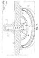
- FIG. 1is a schematic cross-sectional view of one embodiment of a chamber including a gas delivery apparatus adapted for atomic layer deposition.
- FIG. 2is a top cross-sectional view of one embodiment of the expanding channel of the chamber lid of FIG. 1 .
- FIG. 3is a cross-sectional view of the expanding channel of the chamber lid of FIG. 1 .
- FIG. 4is a schematic cross-sectional view illustrating the flow of a gas at two different positions between the surface of a substrate and the bottom surface of the chamber lid of FIG. 1 .
- FIG. 5is a top cross-sectional view of another embodiment of the expanding channel of the chamber lid which is adapted to receive a single gas flow.
- FIG. 6is a top cross-sectional view of another embodiment of the expanding channel of the chamber lid which is adapted to receive three gas flows.
- FIG. 7is a schematic cross-sectional view of another embodiment of a chamber including a gas delivery apparatus adapted for atomic layer deposition.
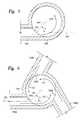
- FIG. 8shows another embodiment of a chamber including a gas delivery apparatus adapted for atomic layer deposition.
- FIG. 9Ais a schematic cross-sectional view of one embodiment of the choke of the chamber lid.
- FIG. 9Bis a cross-sectional view of another embodiment of the choke of the chamber lid.
- FIG. 1is a schematic cross-sectional view of one embodiment of a chamber 200 including a gas delivery apparatus 230 adapted for atomic layer deposition or rapid chemical vapor deposition.
- atomic layer depositionand “rapid chemical vapor deposition” as used herein refer to the sequential introduction of reactants to deposit a thin layer over a substrate structure. The sequential introduction of reactants may be repeated to deposit a plurality of thin layers to form a conformal layer to a desired thickness.
- the chamber 200may also be adapted for other deposition techniques.
- the chamber 200comprises a chamber body 202 having sidewalls 204 and a bottom 206 .
- a slit valve 208 in the chamber 200provides access for a robot (not shown) to deliver and retrieve a substrate 210 , such as a 200 mm or 300 mm semiconductor wafer or a glass substrate, to and from the chamber 200 .
- a substrate support 212supports the substrate 210 on a substrate receiving surface 211 in the chamber 200 .
- the substrate support 212is mounted to a lift motor 214 to raise and lower the substrate support 212 and a substrate 210 disposed thereon.
- a lift plate 216 connected to a lift motor 218is mounted in the chamber 200 and raises and lowers pins 220 movably disposed through the substrate support 212 .
- the pins 220raise and lower the substrate 210 over the surface of the substrate support 212 .
- the substrate support 212may include a vacuum chuck (not shown), an electrostatic chuck (not shown), or a clamp ring (not shown) for securing the substrate 210 to the substrate support 212 during processing.
- the substrate support 212may be heated to heat a substrate 210 disposed thereon.
- the substrate support 212may be heated using an embedded heating element, such as a resistive heater (not shown), or may be heated using radiant heat, such as heating lamps (not shown) disposed above the substrate support 212 .
- a purge ring 222may be disposed on the substrate support 212 to define a purge channel 224 which provides a purge gas to a peripheral portion of the substrate 210 to prevent deposition thereon.
- a gas delivery apparatus 230is disposed at an upper portion of the chamber body 202 to provide a gas, such as a process gas and/or a purge gas, to the chamber 200 .
- a vacuum system 278is in communication with a pumping channel 279 to evacuate any desired gases from the chamber 200 and to help maintain a desired pressure or a desired pressure range inside a pumping zone 266 of the chamber 200 .
- the gas delivery apparatus 230comprises a chamber lid 232 .
- the chamber lid 232includes an expanding channel 234 extending from a central portion of the chamber lid 232 and a bottom surface 260 extending from the expanding channel 234 to a peripheral portion of the chamber lid 232 .
- the bottom surface 260is sized and shaped to substantially cover a substrate 210 disposed on the substrate support 212 .
- the expanding channel 234has gas inlets 236 A, 236 B to provide gas flows from two similar pairs of valves 242 A/ 252 A, 242 B/ 252 B, which may be provided together and/or separately.
- valve 242 A and valve 242 Bare coupled to separate reactant gas sources but are preferably coupled to the same purge gas source.
- valve 242 Ais coupled to reactant gas source 238 and valve 242 B is coupled to reactant gas source 239 , and both valves 242 A, 242 B are coupled to purge gas source 240 .
- Each valve 242 A, 242 Bincludes a delivery line 243 A, 243 B having a valve seat assembly 244 A, 244 B and each valve 252 A, 252 B includes a purge line 245 A, 245 B having a valve seat assembly 246 A, 246 B.
- the delivery line 243 A, 243 Bis in communication with the reactant gas source 238 , 239 and is in communication with the gas inlet 236 A, 236 B of the expanding channel 234 .
- the valve seat assembly 244 A, 244 B of the delivery line 243 A, 243 Bcontrols the flow of the reactant gas from the reactant gas source 238 , 239 to the expanding channel 234 .
- the purge line 245 A, 245 Bis in communication with the purge gas source 240 and intersects the delivery line 243 A, 243 B downstream of the valve seat assembly 244 A, 244 B of the delivery line 243 A, 243 B.
- the valve seat assembly 246 A, 246 B of the purge line 245 A, 245 Bcontrols the flow of the purge gas from the purge gas source 240 to the expanding channel 234 .
- a carrier gasis used to deliver reactant gases from the reactant gas source 238 , 239 , preferably the same gas is used as a carrier gas and a purge gas (i.e. an argon gas used as a carrier gas and a purge gas).
- Each valve seat assembly 244 A, 244 B, 246 A, 246 Bmay comprise a diaphragm (not shown) and a valve seat (not shown).
- the diaphragmmay be biased open or closed and may be actuated closed or open respectively.
- the diaphragmsmay be pneumatically actuated or may be electrically actuated. Examples of pneumatically actuated valves include pneumatically actuated valves available from Fujiken, Inc. and Venflow, Corp. Examples of electrically actuated valves include electrically actuated valves available from Fujiken, Inc.
- Programmable logic controllers 248 A, 248 Bmay be coupled to the valves 242 A, 242 B to control actuation of the diaphragms of the valve seat assemblies 244 A, 244 B, 246 A, 246 B of the valves 242 A, 242 B.
- Pneumatically actuated valvesmay provide pulses of gases in time periods as low as about 0.020 seconds.
- Electrically actuated valvesmay provide pulses of gases in time periods as low as about 0.005 seconds.
- An electrically actuated valvetypically requires the use of a driver coupled between the valve and the programmable logic controller.
- Each valve 242 A, 242 Bmay be a zero dead volume valve to enable flushing of a reactant gas from the delivery line 243 A, 243 B when the valve seat assembly 244 A, 244 B is closed.
- the purge line 245 A, 245 Bmay be positioned adjacent the valve seat assembly 244 A, 244 B of the delivery line 243 A, 243 B.
- the purge line 245 A, 245 Bmay provide a purge gas to flush the delivery line 243 A, 2436 .
- the purge line 245 A, 245 Bis positioned slightly spaced from the valve seat assembly 244 A, 244 B of the delivery line 243 A, 243 B so that a purge gas is not directly delivered into the valve seat assembly 244 A, 244 B when open.
- a zero dead volume valve as used hereinis defined as a valve which has negligible dead volume (i.e. not necessary zero dead volume.)
- Each valve pair 242 A/ 252 A, 242 B/ 252 Bmay be adapted to provide a combined gas flow and/or separate gas flows of the reactant gas and the purge gas.
- a combined gas flow of the reactant gas and the purge gascomprises a continuous flow of a purge gas from the purge gas source 240 through purge line 245 A and pulses of a reactant gas from the reactant gas source 238 through delivery line 243 A.
- the continuous flow of the purge gasmay be provided by leaving the diaphragm of the valve seat assembly 246 A of the purge line 245 A open.
- the pulses of the reactant gas from the reactant gas source 238may be provided by opening and closing the diaphragm of the valve seat assembly 244 A of the delivery line 243 A.
- one example of separate gas flows of the reactant gas and the purge gascomprises pulses of a purge gas from the purge gas source 240 through purge line 245 A and pulses of a reactant gas from the reactant gas source 238 through delivery line 243 A.
- the pulses of the purge gasmay be provided by opening and closing the diaphragm of the valve seat assembly 246 A of the purge line 245 A.
- the pulses of the reactant gas from the reactant gas source 238may be provided by opening and closing the diaphragm of the valve seat assembly 244 A of the delivery line 243 A.
- the delivery lines 243 A, 243 B of the valves 242 A, 242 Bmay be coupled to the gas inlets 236 A, 236 B through gas conduits 250 A, 250 B.
- the gas conduits 250 A, 250 Bmay be integrated or may be separate from the valves 242 A, 242 B.
- the valves 242 A, 242 Bare coupled in close proximity to the expanding channel 234 to reduce any unnecessary volume of the delivery line 243 A, 243 B and the gas conduits 250 A, 250 B between the valves 242 A, 242 B and the gas inlets 236 A, 236 B.
- each gas conduit 250 A, 250 B and gas inlet 236 A, 236 Bmay be positioned in any relationship to a longitudinal axis 290 of the expanding channel 234 .
- the diameter of the gas conduits 250 A, 250 Bmay be increasing from the delivery lines 243 A, 243 B of the valves 242 A, 242 B to the gas inlet 236 A, 236 B to help reduce the velocity of the gas flow prior to its entry into the expanding channel 234 .
- the gas conduits 250 A, 250 Bmay comprise an inner diameter which is gradually increasing or may comprise a plurality of connected conduits having increasing inner diameters.
- the expanding channel 234comprises a channel which has an inner diameter which increases from an upper portion 237 to a lower portion 235 of the expanding channel 234 adjacent the bottom surface 260 of the chamber lid 232 .
- the inner diameter of the expanding channel 234 for a chamber adapted to process 200 mm diameter substratesis between about 0.2 inches and about 1.0 inches, preferably between about 0.3 inches and about 0.9 inches, and more preferably between 0.3 inches and about 0.5 inches at the upper portion 237 of the expanding channel 234 and between about 0.5 inches and about 3.0 inches, preferably between about 0.75 inches and about 2.5 inches, and more preferably between about 1.1 inches and about 2.0 inches at the lower portion 235 of the expanding channel 234 .
- the expanding channel 234may be shaped as a truncated cone (including shapes resembling a truncated cone). Whether a gas is provided toward the walls of the expanding channel 234 or directly downward towards the substrate 210 , the velocity of the gas flow decreases as the gas flow travels through the expanding channel 234 due to the expansion of the gas. The reduction of the velocity of the gas flow helps reduce the likelihood the gas flow will blow off reactants absorbed on the surface of the substrate 210 .
- the diameter of the expanding channel 234which is gradually increasing from the upper portion 237 to the lower portion 235 of the expanding channel 234 , allows less of an adiabatic expansion of a gas through the expanding channel 234 which helps to control the temperature of the gas.
- a sudden adiabatic expansion of a gas delivered through the gas inlet 236 A, 236 B into the expanding channel 234may result in a drop in the temperature of the gas which may cause condensation of the gas and formation of droplets.
- a gradually expanding channel 234according to embodiments of the present invention is believed to provide less of an adiabatic expansion of a gas.
- the gradually expanding channel 234may comprise one or more tapered inner surfaces, such as a tapered straight surface, a concave surface, a convex surface, or combinations thereof or may comprise sections of one or more tapered inner surfaces (i.e. a portion tapered and a portion non-tapered).
- the gas inlets 236 A, 236 Bare located adjacent the upper portion 237 of the expanding channel 234 . In other embodiments, one or more gas inlets 236 A, 236 B may be located along the length of the expanding channel 234 between the upper portion 237 and the lower portion 235 .
- FIG. 2is a top cross-sectional view of one embodiment of the expanding section 234 of the chamber lid 232 of FIG. 1 .
- Each gas conduit 250 A, 250 Bmay be positioned at an angle ⁇ from the center line 302 A, 302 B of the gas conduit 250 A, 250 B and from a radius line 304 from the center of the expanding channel 234 .
- Entry of a gas through the gas conduit 250 A, 250 Bpreferably positioned at an angle ⁇ (i.e., when ⁇ >0° ) causes the gas to flow in a circular direction as shown by arrow 310 A (or 310 B).
- Providing gas at an angle ⁇ as opposed to directly straight-on to the walls of the expanding channeli.e.
- gas conduits 250 A, 250 B and the corresponding gas inlets 236 A, 236 Bare spaced out from each other and direct a flow in the same circular direction (i.e., clockwise or counter-clockwise).
- FIG. 3is a cross-sectional view of the expanding channel 234 of a chamber lid 232 showing simplifled representations of two gas flows therethrough.
- the circular flow 310FIG. 2
- the circular flow 310may travel as a “vortex,” “helix,” or “spiral” flow through the expanding channel 234 as shown by arrows 402 A, 402 B (hereinafter “vortex” flow 402 ).
- the circular flowmay be provided in a “processing region” as opposed to in a compartment separated from the substrate 210 .
- the vortex flowmay help to establish a more efficient purge of the expanding channel 234 due to the sweeping action of the vortex flow pattern across the inner surface of the expanding channel 234 .
- the distance 410 between the gas inlets 236 A, 236 B and the substrate 210is made long enough that the “vortex” flow 402 dissipates to a downwardly flow as shown by arrows 404 as a spiral flow across the surface of the substrate 210 may not be desirable. It is believed that the “vortex” flow 402 and the downwardly flow 404 proceeds in a laminar manner efficiently purging the surface of the chamber lid 232 and the substrate 210 .
- the distance 410 between the upper portion 237 of the expanding channel 234 and the substrate 210is about 1.0 inches or more, preferably about 2.0 inches or more. In one specific embodiment, the upper limit of the distance 410 is dictated by practical limitations.
- the distance 410is very long, then the residence time of a gas traveling though the expanding channel 234 would be long, then the time for a gas to deposit onto the substrate would be long, and then throughput would be low. In addition, if distance 410 is very long, manufacturing of the expanding channel 234 would be difficult.
- the upper limit of distance 410may be 3 inches for a chamber adapted to process 200 mm diameter substrates or 5 inches for a chamber adapted to process 300 mm diameter substrates.
- the bottom surface 260 of the chamber lid 232may be tapered from the expanding channel 234 to a peripheral portion of the chamber lid 232 to help provide an improved velocity profile of a gas flow from the expanding channel 234 across the surface of the substrate 210 (i.e., from the center of the substrate to the edge of the substrate).
- the bottom surface 260may comprise one or more tapered surfaces, such as a straight surface, a concave surface, a convex surface, or combinations thereof.
- the bottom surface 260is tapered in the shape of a funnel.
- FIG. 4is schematic view illustrating the flow of a gas at two different positions 502 , 504 between the bottom surface 260 of the chamber lid 232 and the surface of a substrate 210 .
- Qis the flow of the gas
- Ais the area of the flow section
- Vis the velocity of the gas.
- the velocity of a gasis inversely proportional to the height “H” of the flow section and the radius “R” of the flow section.
- the velocity of the gasmay be theoretically made equal by having the area “A” of the flow sections equal.
- the height H 1 at position 502must be greater than the height H 2 at position 504 .
- the bottom surface 260is downwardly sloping to help reduce the variation in the velocity of the gases as it travels between the bottom surface 260 of the chamber lid 232 and the substrate 210 to help provide uniform exposure of the surface of the substrate 210 to a reactant gas.
- the ratio of the maximum area of the flow section over the minimum area of the flow section between a downwardly sloping bottom surface 260 of the chamber lid 232 and the surface of the substrate 210is less than about 2, preferably less than about 1.5, more preferably less than about 1.3, and most preferably about 1.
- a gas flow traveling at a more uniform velocity across the surface of the substrate 210helps. provide a more uniform deposition of the gas on the substrate 210 .
- the velocity of the gasis directly proportional to the concentration of the gas which is in turn directly proportional to the deposition rate of the gas on the substrate 210 surface.
- a higher velocity of a gas at a first area of the surface of the substrate 210 versus a second area of the surface of the substrate 210is believed to provide a higher deposition of the gas on the first area.
- a chamber lid 232 having a downwardly sloping bottom surface 260provides for more uniform deposition of the gas across the surface of the substrate 210 because the downwardly sloping bottom surface 260 provides a more uniform velocity and, thus, a more uniform concentration of the gas across the surface of the substrate 210 .
- the chamber lid 232may have a choke 262 at a peripheral portion of the chamber lid 232 adjacent the periphery of the substrate 210 .
- the choke 262when the chamber lid 232 is assembled to form a processing zone around the substrate 210 , comprises any member restricting the flow of gas therethrough at an area adjacent the periphery of the substrate 210 .
- FIG. 9Ais a schematic cross-sectional view of one embodiment of the choke 262 .
- the choke 262comprises a circumferential lateral portion 267 .
- the purge ring 222may be adapted to direct a purge gas toward the lateral portion 267 of the choke 262 .
- the choke 262comprises a circumferential downwardly extending protrusion 268 .
- the purge ring 222may be adapted to direct a purge gas toward the circumferential downwardly extending protrusion 268 .
- the thickness of the downwardly extending protrusion 268is between about 0.01 inches and about 1.0 inch, preferably between 0.01 inches and 0.5 inches.
- the spacing between the choke 262 and the substrate support 212is between about 0.04 inches and about 2.0 inches, and preferably between 0.04 inches and about 0.2 inches. The spacing may vary depending on the gases being delivered and the process conditions during deposition.
- the choke 262helps provide a more uniform pressure distribution within the volume or a reaction zone 264 defined between the chamber lid 232 and the substrate 210 by isolating the reaction zone 264 from the non-uniform pressure distribution of the pumping zone 266 (FIG. 1 ).
- a reactant gas or purge gasneeds only adequately fill the reaction zone 264 to ensure sufficient exposure of the substrate 210 to the reactant gas or purge gas.
- prior art chambersare required to provide a combined flow of reactants simultaneously and uniformly to the entire surface of the substrate in order to ensure that the co-reaction of the reactants occurs uniformly across the surface of the substrate 210 .
- the present chamber 200sequentially introduces reactants to the substrate 210 surface to provide absorption of alternating thin layers of the reactants onto the surface of the substrate 210 .
- atomic layer depositiondoes not require a flow of a reactant which reaches the surface of the substrate 210 simultaneously. Instead, a flow of a reactant needs to be provided in an amount which is sufficient to absorb a thin layer of the reactant on the surface of the substrate 210 .
- the reaction zone 264may comprise a smaller volume when compared to the inner volume of a conventional CVD chamber, a smaller amount of gas is required to fill the reaction zone 264 for a particular process in an atomic layer deposition sequence.
- the volume of the reaction zone 264is about 1000 cm 3 or less, preferably 500 cm 3 or less, and more preferably 200 cm 3 or less for a chamber adapted to process 200 mm diameter substrates.
- the volume of the reaction zone 264is about 3,000 cm 3 or less, preferably 1,500 cm 3 or less, and more preferably 600 cm 3 or less for a chamber adapted to process 300 mm diameter substrates.
- the substrate support 212may be raised or lowered to adjust the volume of the reaction zone 264 for deposition. Because of the smaller volume of the reaction zone 264 , less gas, whether a deposition gas or a purge gas, is necessary to be flowed into the chamber 200 . Therefore, the throughput of the chamber 200 is greater and the waste may be minimized due to the smaller amount of gas used reducing the cost of operation.
- the chamber lid 232may include cooling elements and/or heating elements depending on the particular gas being delivered therethrough. Controlling the temperature of the chamber lid 232 may be used to prevent gas decomposition, deposition, or condensation on the chamber lid 232 .
- water channelsmay be formed in the chamber lid 232 to cool the chamber lid 232 .
- heating elementsmay be embedded or may surround components of the chamber lid 232 to heat the chamber lid 232 .
- components of the chamber lid 232may be individually heated or cooled.
- the chamber lid 232may comprise a chamber plate portion 270 and a cap portion 272 in which the chamber plate portion 270 and the cap portion 272 form the expanding channel 234 .
- the cap portion 272may be maintained at one temperature range and the chamber plate portion 270 may be maintained at another temperature range.
- the cap 272may be heated by being wrapped in heater tape or by using another heating device to prevent condensation of reactant gases and the chamber plate portion 270 may be maintained at ambient temperature.
- the cap 272may be heated and the chamber plate portion 270 may be cooled with water channels formed therethrough to prevent thermal decomposition of reactant gases on the chamber plate portion 270 .
- the chamber lid 232may be made of stainless steel, aluminum, nickel-plated aluminum, nickel, or other suitable materials compatible with the processing to be performed.
- the cap portion 272comprises stainless steel and the chamber plate portion 270 comprises aluminum.
- the optional additional plate disposed therebetweencomprises stainless steel.
- the expanding channel 234 and the bottom surface 260 of the chamber lid 232may comprise a mirror polished surface to help produce a laminar flow of a gas along the expanding channel 234 and the bottom surface 260 of the chamber lid 232 .
- the inner surface of the gas conduits 250 A, 250 Bmay be electropolished to help produce a laminar flow of a gas therethrough.
- a control unit 280such as a programmed personal computer, work station computer, or the like, may be coupled to the chamber 200 to control processing conditions.
- the control unit 280may be configured to control flow of various process gases and purge gases from gas sources 238 , 239 , 240 through the valves 242 A, 242 B during different stages of a substrate process sequence.
- the control unit 280comprises a central processing unit (CPU) 282 , support circuitry 284 , and memory 286 containing associated control software 283 .
- CPUcentral processing unit
- the control unit 280may be one of any form of general purpose computer processor that can be used in an industrial setting for controlling various chambers and sub-processors.
- the CPU 282may use any suitable memory 286 , such as random access memory, read only memory, floppy disk drive, hard disk, or any other form of digital storage, local or remote.
- Various support circuitsmay be coupled to the CPU 282 for supporting the chamber 200 .
- the control unit 280may be coupled to another controller that is located adjacent individual chamber components, such as the programmable logic controllers 248 A, 248 B of the valves 242 A, 242 B. Bi-directional communications between the control unit 280 and various other components of the chamber 200 are handled through numerous signal cables collectively referred to as signal buses 288 , some of which are illustrated in FIG.
- control unit 280may be configured to be responsible for automated control of other activities used in wafer processing—such as wafer transport, temperature control, chamber evacuation, among other activities, some of which are described elsewhere herein.
- a substrate 210is delivered to the chamber 200 through the opening 208 by a robot (not shown).
- the substrate 210is positioned on the substrate support 212 through cooperation of the lift pins 220 and the robot.
- the substrate support 212raises the substrate 210 into close opposition to the bottom surface 260 of the chamber lid 232 .
- a first gas flowmay be injected into the expanding channel 234 of the chamber 200 by valve 242 A together or separately (i.e. pulses) with a second gas flow injected into the chamber 200 by valve 242 B.
- the first gas flowmay comprise a continuous flow of a purge gas from purge gas source 240 and pulses of a reactant gas from reactant gas source 238 or may comprise pulses of a reactant gas from reactant gas source 238 and pulses of a purge gas from purge gas source 240 .
- the second gas flowmay comprises a continuous flow of a purge gas from purge gas source 240 and pulses of a reactant gas from reactant gas source 239 or may comprise pulses of a reactant gas from reactant gas source 239 and pulses of a purge gas from purge gas source 240 .
- the gas flowtravels through the expanding channel 234 as a vortex flow pattern 402 which provides a sweeping action across the inner surface of the expanding channel 234 .
- the vortex flow pattern 402dissipates to a downwardly flow 404 toward the surface of the substrate 210 .
- the velocity of the gas flowreduces as it travels through the expanding channel 234 .
- the gas flowthen travels across the surface of the substrate 210 and across the bottom surface 260 of the chamber lid 232 .
- the bottom surface 260 of the chamber lid 232which is downwardly sloping, helps reduce the variation of the velocity of the gas flow across the surface of the substrate 210 .
- the gas flowthen travels by the choke 262 and into the pumping zone 266 of the chamber 200 . Excess gas, by-products, etc. flow into the pumping channel 279 and are then exhausted from the chamber 200 by a vacuum system 278 .
- the gas flowproceeds through the expanding channel 234 and between the surface of the substrate 210 and the bottom surface 260 of the chamber lid 232 in a laminar manner which aids in uniform exposure of a reactant gas to the surface of the substrate 210 and efficient purging of inner surfaces of the chamber lid 232 .
- FIG. 8shows another embodiment of a chamber 900 including a gas delivery apparatus 930 comprising a chamber lid 932 which provides a reaction zone 964 comprising a small volume and which provides a downwardly sloping or funnel shaped bottom surface 960 .
- a gas delivery apparatus 930comprising a chamber lid 932 which provides a reaction zone 964 comprising a small volume and which provides a downwardly sloping or funnel shaped bottom surface 960 .
- Gas sources 937are coupled to the passageway 933 through one or more valves 941 .
- the passageway 933comprises a long length to reduce the likelihood that a gas introduced through valve 941 will blow off reactants absorbed on the surface of the substrate 210 .
- the gas delivery apparatuses 230 , 830 , 930 of FIGS. 1-8have been described above as comprising chamber lids 232 , 832 , 932 which act as the lid of the chamber body 202 .
- Other embodiments of the chamber lids 232 , 832 , 932comprises any covering member disposed over the substrate support 212 delineating a reaction zone 264 , 864 , 964 which lowers the volume in which a gas must flow during substrate processing.
- the chamber lid 232 , 832 , 932may be adapted to move up and down to adjust the volume of the reaction zone 264 , 864 , 964 .
- the gas delivery apparatus 230 of FIG. 1has been described as including two pairs of valves 242 A/ 252 A, 242 B/ 252 B coupled to a reactant gas source 238 , 239 and a purge gas source 240 .
- the gas delivery apparatus 230may comprise one or more valves coupled to a single or a plurality of gas sources in a variety of configurations.
- FIGS. 1-3show a chamber 200 adapted to provide two gas flows together or separately from two gas inlets 236 A, 236 B utilizing two pairs of valves 242 A/ 252 A, 242 B/ 252 B.
- FIG. 5is a top cross-sectional view of another embodiment of an expanding channel 634 of the chamber lid 232 which is adapted to receive a single gas flow through one gas inlet 636 from one gas conduit 650 coupled to a single or a plurality of valves.
- the gas conduit 650may be positioned at an angle ⁇ from the center line 602 of the gas conduit 650 and from a radius line 604 from the center of the expanding channel 634 .
- the gas conduit 650 positioned at an angle ⁇causes a gas to flow in a circular direction as shown by arrow 610 .
- Embodiments of chambers 200 , 800 , 900 with gas delivery apparatuses 230 , 830 , 930 as described in FIGS. 1-8may be used to advantage to implement atomic layer deposition processes of elements, which include but are not limited to, tantalum, titanium, tungsten, and copper, or to implement atomic layer deposition of compounds or alloys/combinations films, which include but are not limited to tantalum nitride, tantalum silicon nitride, titanium nitride, titanium silicon nitride, tungsten nitride, tungsten silicon nitride, and copper aluminum.
- Embodiments of chambers 200 , 800 , 900 with gas delivery apparatuses 230 , 830 , 930 as described in FIGS. 1-8may also be used to advantage to implement chemical vapor deposition of various materials.
- atomic layer deposition of a tantalum nitride barrier layercomprises sequentially providing pulses of a tantalum containing compound and pulses of a nitrogen containing compound to the process chamber 200 in which each pulse is separated by a flow of a purge gas and/or chamber evacuation to remove any excess reactants to prevent gas phase reactions of the tantalum containing compound with the nitrogen containing compound and to remove any reaction by-products.
- Sequentially providing a tantalum containing compound and a nitrogen containing compoundmay result in the alternating absorption of monolayers of a tantalum containing compound and of monolayers of a nitrogen containing compound to form a monolayer of tantalum nitride on a substrate structure for each cycle of pulses.
- substrate structureis used to refer to the substrate as well as other material layers formed thereover, such as a dielectric layer.
- the absorption processes used to absorb the monolayer of the reactantsare self-limiting in that only one monolayer may be absorbed onto the surface of the substrate structure during a given pulse because the surface of the substrate structure has a finite number of sites for absorbing the reactants. Once the finite number of sites are occupied by the reactants, such as the tantalum containing compound or the nitrogen containing compound, further absorption of the reactants will be blocked. The cycle may be repeated to a desired thickness of the tantalum nitride layer.
- Pulses of a tantalum containing compoundsuch as pentadimethylamino-tantalum (PDMAT; Ta(NMe 2 ) 5 ), may be introduced by gas source 238 through valve 242 A.
- the tantalum containing compoundmay be provided with the aid of a carrier gas, which includes, but is not limited to, helium (He), argon (Ar), nitrogen (N 2 ), hydrogen (H 2 ), and combinations thereof.
- Pulses of a nitrogen containing compound, such as ammoniamay be introduced by gas source 239 through valve 242 A.
- a carrier gasmay also be used to help deliver the nitrogen containing compound.
- a purge gas, such as argonmay be introduced by gas source 240 through valve 242 A and/or through valve 242 B.
- the flow of purge gasmay be continuously provided by gas sources 240 through valves 242 A, 242 B to act as a purge gas between the pulses of the tantalum containing compound and of the nitrogen containing compound and to act as a carrier gas during the pulses of the tantalum containing compound and the nitrogen containing compound.
- delivering a purge gas through two gas conduits 250 A, 250 Bprovides a more complete purge of the reaction zone 264 rather than a purge gas provided through one gas conduit 250 A, 250 B.
- a reactant gasmay be delivered through one gas conduit 250 A, 250 B since uniformity of flow of a reactant gas, such as a tantalum containing compound or a nitrogen containing compound, is not as critical as uniformity of the purge gas due to the self-limiting absorption process of the reactants on the surface of substrate structures.
- a purge gasmay be provided in pulses.
- a purge gasmay be provided in more or less than two gas flows.
- a tantalum containing gasmay be provided in more than a single gas flow (i.e. two or more gas flows).
- a nitrogen containingmay be provided in more than a single gas flow (i.e. two or more gas flows).
- tantalum containing compoundsinclude, but are not limited to, other organo-metallic precursors or derivatives thereof, such as pentaethylmethylamino-tantalum (PEMAT; Ta[N(C 2 H 5 CH 3 ) 2 ] 5 ), pentadiethylamino-tantalum (PDEAT; Ta(NEt 2 ) 5 ,), and any and all derivatives of PEMAT, PDEAT, or PDMAT.
- PEMATpentaethylmethylamino-tantalum
- PDEATpentadiethylamino-tantalum
- Ta(NEt 2 ) 5any and all derivatives of PEMAT, PDEAT, or PDMAT.
- tantalum containing compoundsinclude without limitation TBTDET (Ta(NEt 2 ) 3 NC 4 H 9 or C 16 H 39 N 4 Ta) and tantalum halides, for example TaX 5 where X is fluorine (F), bromine (Br) or chlorine (CI), and/or derivatives thereof.
- nitrogen containing compoundsmay be used which include, but are not limited to, N X H Y with x and y being integers (e.g., hydrazine (N 2 H 4 )), dimethyl hydrazine ((CH 3 ) 2 N 2 H 2 ), t-butylhydrazine (C 4 H 9 N 2 H 3 ) phenylhydrazine (C 6 H 5 N 2 H 3 ), other hydrazine derivatives, a nitrogen plasma source (e.g., N 2 , N 2 /H 2 , NH 3 , or a N 2 H 4 plasma), 2,2′-azoisobutane ((CH 3 ) 6 C 2 N 2 ), ethylazide (C 2 H 5 N 3 ), and other suitable gases.
- purge gasesinclude, but are not limited to, helium (He), nitrogen (N 2 ), hydrogen (H 2 ), other gases, and combinations thereof.
- the tantalum nitride layer formationis described as starting with the absorption of a monolayer of a tantalum containing compound on the substrate followed by a monolayer of a nitrogen containing compound.
- the tantalum nitride layer formationmay start with the absorption of a monolayer of a nitrogen containing compound on the substrate followed by a monolayer of the tantalum containing compound.
- a pump evacuation alone between pulses of reactant gasesmay be used to prevent mixing of the reactant gases.
- the time duration for each pulse of the tantalum containing compound, the time duration for each pulse of the nitrogen containing compound, and the duration of the purge gas flow between pulses of the reactantsare variable and depend on the volume capacity of a deposition chamber employed as well as a vacuum system coupled thereto. For example, (1) a lower chamber pressure of a gas will require a longer pulse time; (2) a lower gas flow rate will require a longer time for chamber pressure to rise and stabilize requiring a longer pulse time; and (3) a large-volume chamber will take longer to fill, longer for chamber pressure to stabilize thus requiring a longer pulse time. Similarly, time between each pulse is also variable and depends on volume capacity of the process chamber as well as the vacuum system coupled thereto.
- the time duration of a pulse of the tantalum containing compound or the nitrogen containing compoundshould be long enough for absorption of a monolayer of the compound.
- a pulse of a tantalum containing compoundmay still be in the chamber when a pulse of a nitrogen containing compound enters.
- the duration of the purge gas and/or pump evacuationshould be long enough to prevent the pulses of the tantalum containing compound and the nitrogen containing compound from mixing together in the reaction zone.
- a pulse time of about 1.0 second or less for a tantalum containing compound and a pulse time of about 1.0 second or less for a nitrogen containing compoundare typically sufficient to absorb alternating monolayers on a substrate structure.
- a time of about 1.0 second or less between pulses of the tantalum containing compound and the nitrogen containing compoundis typically sufficient for the purge gas, whether a continuous purge gas or a pulse of a purge gas, to prevent the pulses of the tantalum containing compound and the nitrogen containing compound from mixing together in the reaction zone.
- a longer pulse time of the reactantsmay be used to ensure absorption of the tantalum containing compound and the nitrogen containing compound and a longer time between pulses of the reactants may be used to ensure removal of the reaction by-products.
- the substrate 210may be maintained approximately below a thermal decomposition temperature of a selected tantalum containing compound.
- An exemplary heater temperature range to be used with tantalum containing compounds identified hereinis approximately between about 20° C. and about 500° C. at a chamber pressure less than about 100 torr, preferably less than 50 torr.
- the heater temperatureis preferably between about 100° C. and about 300° C., more preferably between about 175° C. and 250° C.
- the chamber pressureis between about 1.0 and about 5.0 torr.
- a temperature above a thermal decomposition temperaturemay be used.
- the temperatureshould be selected so that more than 50 percent of the deposition activity is by absorption processes.
- a temperature above a thermal decomposition temperaturemay be used in which the amount of decomposition during each precursor deposition is limited so that the growth mode will be similar to an atomic layer deposition growth mode.
- One exemplary process of depositing a tantalum nitride layer by atomic layer deposition, in the process chamber 200 of FIGS. 1-4comprises providing pulses of pentadimethylamino-tantalum (PDMAT) from gas source 238 at a flow rate between about 100 sccm and about 1000 sccm, preferably between about 100 sccm and about 400 sccm, through valve 242 A for a pulse time of about 0.5 seconds or less, about 0.1 seconds or less, or about 0.05 seconds or less due the smaller volume of the reaction zone 264 .
- PDMATpentadimethylamino-tantalum
- Pulses of ammoniamay be provided from gas source 239 at a flow rate between about 100 sccm and about 1000 sccm, preferably between 200 sccm and about 600 sccm, through valve 242 B for a pulse time of about 0.5 seconds or less, about 0.1 seconds or less, or about 0.05 seconds or less due to a smaller volume of the reaction zone 264 .
- An argon purge gas at a flow rate between about 100 sccm and about 1000 sccm, preferably, between about 100 sccm and about 400 sccm,may be continuously provided from gas source 240 through valves 242 A, 242 B.
- the time between pulses of the tantalum containing compound and the nitrogen containing compoundmay be about 0.5 seconds or less, about 0.1 seconds or less, or about 0.07 seconds or less due to the smaller volume of the reaction zone 264 . It is believed that a pulse time of about 0.016 seconds or more is required to fill the reaction zone 264 with a reactant gas and/or a purge gas.
- the heater temperaturepreferably is maintained between about 100° C. and about 300° C. at a chamber pressure between about 1.0 and about 5.0 torr. This process provides a tantalum nitride layer in a thickness between about 0.5 ⁇ and about 1.0 ⁇ per cycle. The alternating sequence may be repeated until a desired thickness is achieved.
- the layersuch as a tantalum nitride layer
- the layeris deposited to a sidewall coverage of about 50 ⁇ or less.
- the layeris deposited to a sidewall coverage of about 20 ⁇ or less.
- the layeris deposited to a sidewall coverage of about 10 ⁇ or less.
- a tantalum nitride layer with a thickness of about 10 521 or lessis believed to be a sufficient thickness in the application as a barrier layer to prevent copper diffusion.
- a thin barrier layermay be used to advantage in filling sub-micron (e.g., less than 0.15 ⁇ m) and smaller features having high aspect ratios (e.g., greater than 5 to 1).
- a layer having a sidewall coverage of greater than 50 ⁇may be used.
- Embodiments of atomic layer depositionhave been described above as absorption of a monolayer of reactants on a substrate.
- the present inventionalso includes embodiments in which the reactants are deposited to more or less than a monolayer.
- the present inventionalso includes embodiments in which the reactants are not deposited in a self-limiting manner.
- the present inventionalso includes embodiments in which deposition occurs in mainly a chemical vapor deposition process in which the reactants are delivered sequentially or simultaneously.
- Embodiments of atomic layer depositionhave been described above as the deposition of the binary compound of tantalum nitride utilizing pulses of two reactants. In the deposition of other elements or compounds, pulses of two or more reactants may also be used.
Landscapes
- Chemical & Material Sciences (AREA)
- Engineering & Computer Science (AREA)
- General Chemical & Material Sciences (AREA)
- Chemical Kinetics & Catalysis (AREA)
- Organic Chemistry (AREA)
- Metallurgy (AREA)
- Mechanical Engineering (AREA)
- Materials Engineering (AREA)
- Physics & Mathematics (AREA)
- Computer Hardware Design (AREA)
- Power Engineering (AREA)
- Microelectronics & Electronic Packaging (AREA)
- Manufacturing & Machinery (AREA)
- General Physics & Mathematics (AREA)
- Condensed Matter Physics & Semiconductors (AREA)
- Fluid Mechanics (AREA)
- Inorganic Chemistry (AREA)
- Chemical Vapour Deposition (AREA)
- Internal Circuitry In Semiconductor Integrated Circuit Devices (AREA)
- Electrodes Of Semiconductors (AREA)
Abstract
Description
This application claims benefit of U.S. provisional Patent Application Ser. No. 60/346,086, entitled “METHOD AND APPARATUS FOR ALD DEPOSITION,” filed Oct. 26, 2001, which is herein incorporated by reference.
1. Field of the Invention
Embodiments of the present invention generally relate to an apparatus and method for atomic layer deposition. More particularly, embodiments of the present invention relate to an improved gas delivery apparatus and method for atomic layer deposition.
2. Description of the Related Art
Reliably producing sub-micron and smaller features is one of the key technologies for the next generation of very large scale integration (VLSI) and ultra large scale integration (ULSI) of semiconductor devices. However, as the fringes of circuit technology are pressed, the shrinking dimensions of interconnects in VLSI and ULSI technology have placed additional demands on the processing capabilities. The multilevel interconnects that lie at the heart of this technology require precise processing of high aspect ratio features, such as vias and other interconnects. Reliable formation of these interconnects is very important to VLSI and ULSI success and to the continued effort to increase circuit density and quality of individual substrates.
As circuit densities increase, the widths of vias, contacts, and other features, as well as the dielectric materials between them, decrease to sub-micron dimensions (e.g., less than 0.20 micrometers or less), whereas the thickness of the dielectric layers remains substantially constant, with the result that the aspect ratios for the features, i.e., their height divided by width, increase. Many traditional deposition processes have difficulty filling sub-micron structures where the aspect ratio exceeds 4:1, and particularly where the aspect ratio exceeds 10:1. Therefore, there is a great amount of ongoing effort being directed at the formation of substantially void-free and seam-free sub-micron features having high aspect ratios.
Atomic layer deposition is one deposition technique being explored for the deposition of material layers over features having high aspect ratios. One example of atomic layer deposition comprises the sequential introduction of pulses of gases. For instance, one cycle for the sequential introduction of pulses of gases may comprise a pulse of a first reactant gas, followed by a pulse of a purge gas and/or a pump evacuation, followed by a pulse of a second reactant gas, and followed by a pulse of a purge gas and/or a pump evacuation. The term “gas” as used herein is defined to include a single gas or a plurality of gases. Sequential introduction of separate pulses of the first reactant and the second reactant may result in the alternating self-limiting absorption of monolayers of the reactants on the surface of the substrate and, thus, forms a monolayer of material for each cycle. The cycle may be repeated to a desired thickness of the deposited material. A pulse of a purge gas and/or a pump evacuation between the pulses of the first reactant gas and the pulses of the second reactant gas serves to reduce the likelihood of gas phase reactions of the reactants due to excess amounts of the reactants remaining in the chamber.
However, there is a need for new apparatuses to perform gas delivery and to perform deposition of films by atomic layer deposition.
Embodiments of the present invention relate to an improved gas delivery apparatus adapted for atomic layer deposition or rapid chemical vapor deposition. One embodiment of the gas delivery assembly comprises a covering member having an expanding channel at a central portion of the covering member and having a bottom surface extending from the expanding channel to a peripheral portion of the covering member. One or more gas conduits are coupled to the expanding channel in which the one or more gas conduits are positioned at an angle from a center of the expanding channel.
Another embodiment of the gas delivery assembly comprises a first valve and a second valve. The first valve includes a first delivery line and a first purge line. The first delivery line comprises a first reactant gas inlet, a first reactant gas outlet, and a first valve seat assembly. The first purge line comprises a first purge gas inlet and a first purge gas outlet. The first purge gas outlet of the first purge line is in communication with the first delivery line downstream of the first valve seat assembly. The second valve includes a second delivery line and a second purge line. The second delivery line comprises a second reactant gas inlet, a second reactant gas outlet, and a second valve seat assembly. The second purge line comprises a second purge gas inlet and a second purge gas outlet. The second purge gas outlet of the second purge line is in communication with the second delivery line downstream of the second valve seat assembly.
One embodiment of a chamber comprises a substrate support having a substrate receiving surface. The chamber further includes a chamber lid having a passageway at a central portion of the chamber lid and a tapered bottom surface extending from the passageway to a peripheral portion of the chamber lid. The bottom surface of the chamber lid is shaped and sized to substantially cover the substrate receiving surface. One or more valves are coupled to the passageway, and one or more gas sources are coupled to each valve. In one aspect, the bottom surface of the chamber lid may be tapered. In another aspect, a reaction zone defined between the chamber lid and the substrate receiving surface may comprise a small volume. In still another aspect, the passageway may comprise a tapered expanding channel extending from the central portion of the chamber lid.
Another embodiment of the chamber comprises a substrate support having a substrate receiving surface. The chamber further comprises a chamber lid having an expanding channel extending from a central portion of the chamber lid and having a tapered bottom surface extending from the expanding channel to a peripheral portion of the chamber lid. One or more gas conduits are disposed around an upper portion of the expanding channel in which the one or more gas conduits are disposed at an angle from a center of the expanding channel. A choke is disposed on the chamber lid adjacent a perimeter of the tapered bottom surface.
One embodiment of a method of depositing a material layer over a substrate structure comprises delivering a first reactant gas and a first purge gas through a first gas conduit in which the first reactant gas is provided in pulses and the first purge gas is provided in a continuous flow. The method further comprises delivering a second reactant gas and a second purge through a second gas conduit in which the second reactant gas is provided in pulses and the second purge gas is provided in a continuous flow.
One embodiment of a method of delivering gases to a substrate in a substrate processing chamber comprises providing one or more gases into the substrate processing chamber, reducing a velocity of the gases through non-adiabatic expansion, providing the gases to a central portion of the substrate, and directing the gases radially across the substrate from the central portion of the substrate to a peripheral portion of the substrate.
Another embodiment of a method of delivering gases to a substrate in a substrate processing chamber comprises providing one or more gases to a central portion of the substrate and directing the gases radially at a substantially uniform velocity across the substrate from the central portion of the substrate to a peripheral portion of the substrate.
So that the manner in which the above recited features of the present invention are attained and can be understood in detail, a more particular description of the invention, briefly summarized above, may be had by reference to the embodiments thereof which are illustrated in the appended drawings.
It is to be noted, however, that the appended drawings illustrate only typical embodiments of this invention and are therefore not to be considered limiting of its scope, for the invention may admit to other equally effective embodiments.
Thechamber 200 comprises achamber body 202 havingsidewalls 204 and a bottom206. Aslit valve 208 in thechamber 200 provides access for a robot (not shown) to deliver and retrieve asubstrate 210, such as a 200 mm or 300 mm semiconductor wafer or a glass substrate, to and from thechamber 200.
Asubstrate support 212 supports thesubstrate 210 on asubstrate receiving surface 211 in thechamber 200. Thesubstrate support 212 is mounted to alift motor 214 to raise and lower thesubstrate support 212 and asubstrate 210 disposed thereon. Alift plate 216 connected to alift motor 218 is mounted in thechamber 200 and raises and lowerspins 220 movably disposed through thesubstrate support 212. Thepins 220 raise and lower thesubstrate 210 over the surface of thesubstrate support 212. Thesubstrate support 212 may include a vacuum chuck (not shown), an electrostatic chuck (not shown), or a clamp ring (not shown) for securing thesubstrate 210 to thesubstrate support 212 during processing.
Thesubstrate support 212 may be heated to heat asubstrate 210 disposed thereon. For example, thesubstrate support 212 may be heated using an embedded heating element, such as a resistive heater (not shown), or may be heated using radiant heat, such as heating lamps (not shown) disposed above thesubstrate support 212. Apurge ring 222 may be disposed on thesubstrate support 212 to define apurge channel 224 which provides a purge gas to a peripheral portion of thesubstrate 210 to prevent deposition thereon.
Agas delivery apparatus 230 is disposed at an upper portion of thechamber body 202 to provide a gas, such as a process gas and/or a purge gas, to thechamber 200. Avacuum system 278 is in communication with apumping channel 279 to evacuate any desired gases from thechamber 200 and to help maintain a desired pressure or a desired pressure range inside apumping zone 266 of thechamber 200.
In one embodiment, thegas delivery apparatus 230 comprises achamber lid 232. Thechamber lid 232 includes an expandingchannel 234 extending from a central portion of thechamber lid 232 and abottom surface 260 extending from the expandingchannel 234 to a peripheral portion of thechamber lid 232. Thebottom surface 260 is sized and shaped to substantially cover asubstrate 210 disposed on thesubstrate support 212. The expandingchannel 234 hasgas inlets valves 242A/252A,242B/252B, which may be provided together and/or separately.
In one configuration,valve 242A andvalve 242B are coupled to separate reactant gas sources but are preferably coupled to the same purge gas source. For example,valve 242A is coupled toreactant gas source 238 andvalve 242B is coupled toreactant gas source 239, and bothvalves gas source 240. Eachvalve delivery line valve seat assembly valve purge line valve seat assembly delivery line reactant gas source gas inlet channel 234. Thevalve seat assembly delivery line reactant gas source channel 234. Thepurge line purge gas source 240 and intersects thedelivery line valve seat assembly delivery line valve seat assembly purge line purge gas source 240 to the expandingchannel 234. If a carrier gas is used to deliver reactant gases from thereactant gas source
Eachvalve seat assembly Programmable logic controllers valves valve seat assemblies valves
Eachvalve delivery line valve seat assembly purge line valve seat assembly delivery line valve seat assembly purge line delivery line 243A,2436. In the embodiment shown, thepurge line valve seat assembly delivery line valve seat assembly
Eachvalve pair 242A/252A,242B/252B may be adapted to provide a combined gas flow and/or separate gas flows of the reactant gas and the purge gas. In reference tovalve pair 242A/252A, one example of a combined gas flow of the reactant gas and the purge gas comprises a continuous flow of a purge gas from thepurge gas source 240 throughpurge line 245A and pulses of a reactant gas from thereactant gas source 238 throughdelivery line 243A. The continuous flow of the purge gas may be provided by leaving the diaphragm of thevalve seat assembly 246A of thepurge line 245A open. The pulses of the reactant gas from thereactant gas source 238 may be provided by opening and closing the diaphragm of thevalve seat assembly 244A of thedelivery line 243A. In reference tovalve pair 242A/252A, one example of separate gas flows of the reactant gas and the purge gas comprises pulses of a purge gas from thepurge gas source 240 throughpurge line 245A and pulses of a reactant gas from thereactant gas source 238 throughdelivery line 243A. The pulses of the purge gas may be provided by opening and closing the diaphragm of thevalve seat assembly 246A of thepurge line 245A. The pulses of the reactant gas from thereactant gas source 238 may be provided by opening and closing the diaphragm of thevalve seat assembly 244A of thedelivery line 243A.
The delivery lines243A,243B of thevalves gas inlets gas conduits gas conduits valves valves channel 234 to reduce any unnecessary volume of thedelivery line gas conduits valves gas inlets
In reference toFIG. 3 , eachgas conduit gas inlet longitudinal axis 290 of the expandingchannel 234. Eachgas conduit gas inlet longitudinal axis 290 or positioned at an angle +β or an angle −β (in which 0°>+β>90° or 0°>−β>90°) from thecenterline gas conduit longitudinal axis 290. Therefore, thegas conduit longitudinal axis 290 as shown inFIG. 3 , may be angled downwardly at an angle +β, or may be angled upwardly at an angle −β to provide a gas flow toward the walls of the expandingchannel 234 rather than directly downward towards thesubstrate 210 which helps reduce the likelihood of blowing off reactants absorbed on the surface of thesubstrate 210. In addition, the diameter of thegas conduits delivery lines valves gas inlet channel 234. For example, thegas conduits
Referring toFIG. 1 , the expandingchannel 234 comprises a channel which has an inner diameter which increases from anupper portion 237 to alower portion 235 of the expandingchannel 234 adjacent thebottom surface 260 of thechamber lid 232. In one specific embodiment, the inner diameter of the expandingchannel 234 for a chamber adapted to process 200 mm diameter substrates is between about 0.2 inches and about 1.0 inches, preferably between about 0.3 inches and about 0.9 inches, and more preferably between 0.3 inches and about 0.5 inches at theupper portion 237 of the expandingchannel 234 and between about 0.5 inches and about 3.0 inches, preferably between about 0.75 inches and about 2.5 inches, and more preferably between about 1.1 inches and about 2.0 inches at thelower portion 235 of the expandingchannel 234. In another specific embodiment, the inner diameter of the expandingchannel 234 for a chamber adapted to process 300 mm diameter substrates is between about 0.2 inches and about 1.0 inches, preferably between about 0.3 inches and about 0.9 inches, and more preferably between 0.3 inches and about 0.5 inches at theupper portion 237 of the expandingchannel 234 and between about 0.5 inches and about 3.0 inches, preferably between about 0.75 inches and about 2.5 inches, and more preferably between about 1.2 inches and about 2.2 inches at thelower portion 235 of the expandingchannel 234. In general, the above dimension apply to an expanding channel adapted to provide a total gas flow of between about 500 sccm and about 3,000 sccm. In other specific embodiments, the dimension may be altered to accommodate a certain gas flow therethough. In general, a larger gas flow will require a larger diameter expanding channel. In one embodiment, the expandingchannel 234 may be shaped as a truncated cone (including shapes resembling a truncated cone). Whether a gas is provided toward the walls of the expandingchannel 234 or directly downward towards thesubstrate 210, the velocity of the gas flow decreases as the gas flow travels through the expandingchannel 234 due to the expansion of the gas. The reduction of the velocity of the gas flow helps reduce the likelihood the gas flow will blow off reactants absorbed on the surface of thesubstrate 210.
Not wishing to be bound by theory, it is believed that the diameter of the expandingchannel 234, which is gradually increasing from theupper portion 237 to thelower portion 235 of the expandingchannel 234, allows less of an adiabatic expansion of a gas through the expandingchannel 234 which helps to control the temperature of the gas. For instance, a sudden adiabatic expansion of a gas delivered through thegas inlet channel 234 may result in a drop in the temperature of the gas which may cause condensation of the gas and formation of droplets. On the other hand, a gradually expandingchannel 234 according to embodiments of the present invention is believed to provide less of an adiabatic expansion of a gas. Therefore, more heat may be transferred to or from the gas, and, thus, the temperature of the gas may be more easily controlled by controlling the surrounding temperature of the gas (i.e., controlling the temperature of the chamber lid232). The gradually expandingchannel 234 may comprise one or more tapered inner surfaces, such as a tapered straight surface, a concave surface, a convex surface, or combinations thereof or may comprise sections of one or more tapered inner surfaces (i.e. a portion tapered and a portion non-tapered).
In one embodiment, thegas inlets upper portion 237 of the expandingchannel 234. In other embodiments, one ormore gas inlets channel 234 between theupper portion 237 and thelower portion 235.
Not wishing to be bound by theory,FIG. 3 is a cross-sectional view of the expandingchannel 234 of achamber lid 232 showing simplifled representations of two gas flows therethrough. Although the exact flow patted through the expandingchannel 234 is not known, it is believed that the circular flow310 (FIG. 2 ) may travel as a “vortex,” “helix,” or “spiral” flow through the expandingchannel 234 as shown byarrows FIG. 3 , the circular flow may be provided in a “processing region” as opposed to in a compartment separated from thesubstrate 210. In one aspect, the vortex flow may help to establish a more efficient purge of the expandingchannel 234 due to the sweeping action of the vortex flow pattern across the inner surface of the expandingchannel 234.
In one embodiment, thedistance 410 between thegas inlets substrate 210 is made long enough that the “vortex” flow402 dissipates to a downwardly flow as shown byarrows 404 as a spiral flow across the surface of thesubstrate 210 may not be desirable. It is believed that the “vortex” flow402 and thedownwardly flow 404 proceeds in a laminar manner efficiently purging the surface of thechamber lid 232 and thesubstrate 210. In one specific embodiment thedistance 410 between theupper portion 237 of the expandingchannel 234 and thesubstrate 210 is about 1.0 inches or more, preferably about 2.0 inches or more. In one specific embodiment, the upper limit of thedistance 410 is dictated by practical limitations. For example, If thedistance 410 is very long, then the residence time of a gas traveling though the expandingchannel 234 would be long, then the time for a gas to deposit onto the substrate would be long, and then throughput would be low. In addition, ifdistance 410 is very long, manufacturing of the expandingchannel 234 would be difficult. In general, the upper limit ofdistance 410 may be 3 inches for a chamber adapted to process 200 mm diameter substrates or 5 inches for a chamber adapted to process 300 mm diameter substrates.
Referring toFIG. 1 , at least a portion of thebottom surface 260 of thechamber lid 232 may be tapered from the expandingchannel 234 to a peripheral portion of thechamber lid 232 to help provide an improved velocity profile of a gas flow from the expandingchannel 234 across the surface of the substrate210 (i.e., from the center of the substrate to the edge of the substrate). Thebottom surface 260 may comprise one or more tapered surfaces, such as a straight surface, a concave surface, a convex surface, or combinations thereof. In one embodiment, thebottom surface 260 is tapered in the shape of a funnel.
Not wishing to be bound by theory,FIG. 4 is schematic view illustrating the flow of a gas at twodifferent positions bottom surface 260 of thechamber lid 232 and the surface of asubstrate 210. The velocity of the gas at a certain position is theoretically determined by the equation below:
Q/A=V (1)
In which, “Q” is the flow of the gas, “A” is the area of the flow section, and “V” is the velocity of the gas. The velocity of the gas is inversely proportional to the area “A” of the flow section (H=2π R), in which “H” is the height of the flow section and “2πR” is the circumference of the flow section having a radius “R” . In other words, the velocity of a gas is inversely proportional to the height “H” of the flow section and the radius “R” of the flow section.
Comparing the velocity of the flow section atposition 502 andposition 504, assuming that the flow “Q” of the gas at all positions between thebottom surface 260 of thechamber lid 232 and the surface of thesubstrate 210 is equal, the velocity of the gas may be theoretically made equal by having the area “A” of the flow sections equal. For the area of flow sections atposition 502 andposition 504 to be equal, the height H1atposition 502 must be greater than the height H2atposition 504.
In one aspect, thebottom surface 260 is downwardly sloping to help reduce the variation in the velocity of the gases as it travels between thebottom surface 260 of thechamber lid 232 and thesubstrate 210 to help provide uniform exposure of the surface of thesubstrate 210 to a reactant gas. In one embodiment, the ratio of the maximum area of the flow section over the minimum area of the flow section between a downwardly slopingbottom surface 260 of thechamber lid 232 and the surface of thesubstrate 210 is less than about 2, preferably less than about 1.5, more preferably less than about 1.3, and most preferably about 1.
Not wishing to be bound by theory, it is believed that a gas flow traveling at a more uniform velocity across the surface of thesubstrate 210 helps. provide a more uniform deposition of the gas on thesubstrate 210. It is believed that the velocity of the gas is directly proportional to the concentration of the gas which is in turn directly proportional to the deposition rate of the gas on thesubstrate 210 surface. Thus, a higher velocity of a gas at a first area of the surface of thesubstrate 210 versus a second area of the surface of thesubstrate 210 is believed to provide a higher deposition of the gas on the first area. It is believed that achamber lid 232 having a downwardly slopingbottom surface 260 provides for more uniform deposition of the gas across the surface of thesubstrate 210 because the downwardly slopingbottom surface 260 provides a more uniform velocity and, thus, a more uniform concentration of the gas across the surface of thesubstrate 210.
Referring toFIG. 1 , thechamber lid 232 may have achoke 262 at a peripheral portion of thechamber lid 232 adjacent the periphery of thesubstrate 210. Thechoke 262, when thechamber lid 232 is assembled to form a processing zone around thesubstrate 210, comprises any member restricting the flow of gas therethrough at an area adjacent the periphery of thesubstrate 210.FIG. 9A is a schematic cross-sectional view of one embodiment of thechoke 262. In this embodiment, thechoke 262 comprises a circumferentiallateral portion 267. In one aspect, thepurge ring 222 may be adapted to direct a purge gas toward thelateral portion 267 of thechoke 262.FIG. 9B is a schematic cross-sectional view of another embodiment of thechoke 262. In this embodiment, thechoke 262 comprises a circumferential downwardly extendingprotrusion 268. In one aspect, thepurge ring 222 may be adapted to direct a purge gas toward the circumferential downwardly extendingprotrusion 268. In one specific embodiment, the thickness of the downwardly extendingprotrusion 268 is between about 0.01 inches and about 1.0 inch, preferably between 0.01 inches and 0.5 inches.
In one specific embodiment, the spacing between thechoke 262 and thesubstrate support 212 is between about 0.04 inches and about 2.0 inches, and preferably between 0.04 inches and about 0.2 inches. The spacing may vary depending on the gases being delivered and the process conditions during deposition. Thechoke 262 helps provide a more uniform pressure distribution within the volume or areaction zone 264 defined between thechamber lid 232 and thesubstrate 210 by isolating thereaction zone 264 from the non-uniform pressure distribution of the pumping zone266 (FIG.1).
Referring toFIG. 1 , in one aspect, since thereaction zone 264 is isolated from thepumping zone 266, a reactant gas or purge gas needs only adequately fill thereaction zone 264 to ensure sufficient exposure of thesubstrate 210 to the reactant gas or purge gas. In conventional chemical vapor deposition, prior art chambers are required to provide a combined flow of reactants simultaneously and uniformly to the entire surface of the substrate in order to ensure that the co-reaction of the reactants occurs uniformly across the surface of thesubstrate 210. In atomic layer deposition, thepresent chamber 200 sequentially introduces reactants to thesubstrate 210 surface to provide absorption of alternating thin layers of the reactants onto the surface of thesubstrate 210. As a consequence, atomic layer deposition does not require a flow of a reactant which reaches the surface of thesubstrate 210 simultaneously. Instead, a flow of a reactant needs to be provided in an amount which is sufficient to absorb a thin layer of the reactant on the surface of thesubstrate 210.
Since thereaction zone 264 may comprise a smaller volume when compared to the inner volume of a conventional CVD chamber, a smaller amount of gas is required to fill thereaction zone 264 for a particular process in an atomic layer deposition sequence. For example, in one embodiment, the volume of thereaction zone 264 is about 1000 cm3or less, preferably 500 cm3or less, and more preferably 200 cm3or less for a chamber adapted to process 200 mm diameter substrates. In one embodiment, the volume of thereaction zone 264 is about 3,000 cm3or less, preferably 1,500 cm3or less, and more preferably 600 cm3or less for a chamber adapted to process 300 mm diameter substrates. In one embodiment, thesubstrate support 212 may be raised or lowered to adjust the volume of thereaction zone 264 for deposition. Because of the smaller volume of thereaction zone 264, less gas, whether a deposition gas or a purge gas, is necessary to be flowed into thechamber 200. Therefore, the throughput of thechamber 200 is greater and the waste may be minimized due to the smaller amount of gas used reducing the cost of operation.
Thechamber lid 232 has been shown inFIGS. 1-4 as comprising a cap portion272 and achamber plate portion 270 in which the cap portion272 and thechamber plate portion 270 form the expandingchannel 234. An additional plate may be optionally disposed between thechamber lid portion 270 and the cap portion272. In other embodiments, the expandingchannel 234 may be made integrally from a single piece of material.
Thechamber lid 232 may include cooling elements and/or heating elements depending on the particular gas being delivered therethrough. Controlling the temperature of thechamber lid 232 may be used to prevent gas decomposition, deposition, or condensation on thechamber lid 232. For example, water channels (not shown) may be formed in thechamber lid 232 to cool thechamber lid 232. In another example, heating elements (not shown) may be embedded or may surround components of thechamber lid 232 to heat thechamber lid 232. In one embodiment, components of thechamber lid 232 may be individually heated or cooled. For example; referring toFIG. 1 , thechamber lid 232 may comprise achamber plate portion 270 and a cap portion272 in which thechamber plate portion 270 and the cap portion272 form the expandingchannel 234. The cap portion272 may be maintained at one temperature range and thechamber plate portion 270 may be maintained at another temperature range. For example, the cap272 may be heated by being wrapped in heater tape or by using another heating device to prevent condensation of reactant gases and thechamber plate portion 270 may be maintained at ambient temperature. In another example, the cap272 may be heated and thechamber plate portion 270 may be cooled with water channels formed therethrough to prevent thermal decomposition of reactant gases on thechamber plate portion 270.
Thechamber lid 232 may be made of stainless steel, aluminum, nickel-plated aluminum, nickel, or other suitable materials compatible with the processing to be performed. In one embodiment, the cap portion272 comprises stainless steel and thechamber plate portion 270 comprises aluminum. In one embodiment, the optional additional plate disposed therebetween comprises stainless steel. In one embodiment, the expandingchannel 234 and thebottom surface 260 of thechamber lid 232 may comprise a mirror polished surface to help produce a laminar flow of a gas along the expandingchannel 234 and thebottom surface 260 of thechamber lid 232. In another embodiment, the inner surface of thegas conduits
Returning toFIG. 1 , acontrol unit 280, such as a programmed personal computer, work station computer, or the like, may be coupled to thechamber 200 to control processing conditions. For example, thecontrol unit 280 may be configured to control flow of various process gases and purge gases fromgas sources valves control unit 280 comprises a central processing unit (CPU)282,support circuitry 284, andmemory 286 containing associatedcontrol software 283.
Thecontrol unit 280 may be one of any form of general purpose computer processor that can be used in an industrial setting for controlling various chambers and sub-processors. TheCPU 282 may use anysuitable memory 286, such as random access memory, read only memory, floppy disk drive, hard disk, or any other form of digital storage, local or remote. Various support circuits may be coupled to theCPU 282 for supporting thechamber 200. Thecontrol unit 280 may be coupled to another controller that is located adjacent individual chamber components, such as theprogrammable logic controllers valves control unit 280 and various other components of thechamber 200 are handled through numerous signal cables collectively referred to assignal buses 288, some of which are illustrated in FIG.1. In addition to control of process gases and purge gases fromgas sources programmable logic controllers valves control unit 280 may be configured to be responsible for automated control of other activities used in wafer processing—such as wafer transport, temperature control, chamber evacuation, among other activities, some of which are described elsewhere herein.
Referring toFIGS. 1-4 , in operation, asubstrate 210 is delivered to thechamber 200 through theopening 208 by a robot (not shown). Thesubstrate 210 is positioned on thesubstrate support 212 through cooperation of the lift pins220 and the robot. Thesubstrate support 212 raises thesubstrate 210 into close opposition to thebottom surface 260 of thechamber lid 232. A first gas flow may be injected into the expandingchannel 234 of thechamber 200 byvalve 242A together or separately (i.e. pulses) with a second gas flow injected into thechamber 200 byvalve 242B. The first gas flow may comprise a continuous flow of a purge gas frompurge gas source 240 and pulses of a reactant gas fromreactant gas source 238 or may comprise pulses of a reactant gas fromreactant gas source 238 and pulses of a purge gas frompurge gas source 240. The second gas flow may comprises a continuous flow of a purge gas frompurge gas source 240 and pulses of a reactant gas fromreactant gas source 239 or may comprise pulses of a reactant gas fromreactant gas source 239 and pulses of a purge gas frompurge gas source 240. The gas flow travels through the expandingchannel 234 as a vortex flow pattern402 which provides a sweeping action across the inner surface of the expandingchannel 234. The vortex flow pattern402 dissipates to adownwardly flow 404 toward the surface of thesubstrate 210. The velocity of the gas flow reduces as it travels through the expandingchannel 234. The gas flow then travels across the surface of thesubstrate 210 and across thebottom surface 260 of thechamber lid 232. Thebottom surface 260 of thechamber lid 232, which is downwardly sloping, helps reduce the variation of the velocity of the gas flow across the surface of thesubstrate 210. The gas flow then travels by thechoke 262 and into thepumping zone 266 of thechamber 200. Excess gas, by-products, etc. flow into the pumpingchannel 279 and are then exhausted from thechamber 200 by avacuum system 278. In one aspect, the gas flow proceeds through the expandingchannel 234 and between the surface of thesubstrate 210 and thebottom surface 260 of thechamber lid 232 in a laminar manner which aids in uniform exposure of a reactant gas to the surface of thesubstrate 210 and efficient purging of inner surfaces of thechamber lid 232.
For example,FIG. 7 shows another embodiment of achamber 800 including agas delivery apparatus 830 comprising achamber lid 832 which provides a reaction864 zone comprising a small volume and which provides an expanding channel834. Some components of thechamber 800 are the same or similar to those described with reference tochamber 200 ofFIG. 1 , described above. Accordingly, like numbers have been used where appropriate. Thechamber lid 832 comprises a bottom surface860 that is substantially flat. In one embodiment, the spacing between thechoke 262 and thesubstrate support 212 is between about 0.04 inches and about 2.0 inches, preferably between about 0.04 inches and about 0.2 inches.
In another example,FIG. 8 shows another embodiment of achamber 900 including agas delivery apparatus 930 comprising achamber lid 932 which provides areaction zone 964 comprising a small volume and which provides a downwardly sloping or funnel shapedbottom surface 960. Some components of thechamber 900 are the same or similar to those described with reference tochamber 200 ofFIG. 1 , described above. Accordingly, like numbers have been used where appropriate.Gas sources 937 are coupled to thepassageway 933 through one ormore valves 941. In one aspect, thepassageway 933 comprises a long length to reduce the likelihood that a gas introduced throughvalve 941 will blow off reactants absorbed on the surface of thesubstrate 210.
Thegas delivery apparatuses FIGS. 1-8 have been described above as comprisingchamber lids chamber body 202. Other embodiments of thechamber lids substrate support 212 delineating areaction zone substrate support 212, thechamber lid reaction zone
Thegas delivery apparatus 230 ofFIG. 1 has been described as including two pairs ofvalves 242A/252A,242B/252B coupled to areactant gas source purge gas source 240. In other embodiments, thegas delivery apparatus 230 may comprise one or more valves coupled to a single or a plurality of gas sources in a variety of configurations.FIGS. 1-3 show achamber 200 adapted to provide two gas flows together or separately from twogas inlets valves 242A/252A,242B/252B.FIG. 5 is a top cross-sectional view of another embodiment of an expandingchannel 634 of thechamber lid 232 which is adapted to receive a single gas flow through onegas inlet 636 from onegas conduit 650 coupled to a single or a plurality of valves. Thegas conduit 650 may be positioned at an angle α from thecenter line 602 of thegas conduit 650 and from aradius line 604 from the center of the expandingchannel 634. Thegas conduit 650 positioned at an angle α (i.e., when α>0° ) causes a gas to flow in a circular direction as shown byarrow 610.FIG. 6 is a top cross-sectional view of another embodiment of an expandingchannel 734 of thechamber lid 232 which is adapted to receive three gas flows together, partially together (i.e. two of three gas flows together), or separately through threegas inlets gas conduits gas conduits center line 702 of thegas conduits radius line 704 from the center of the expandingchannel 734. Thegas conduits arrows 710.
Embodiments ofchambers gas delivery apparatuses FIGS. 1-8 may be used to advantage to implement atomic layer deposition processes of elements, which include but are not limited to, tantalum, titanium, tungsten, and copper, or to implement atomic layer deposition of compounds or alloys/combinations films, which include but are not limited to tantalum nitride, tantalum silicon nitride, titanium nitride, titanium silicon nitride, tungsten nitride, tungsten silicon nitride, and copper aluminum. Embodiments ofchambers gas delivery apparatuses FIGS. 1-8 may also be used to advantage to implement chemical vapor deposition of various materials.
For clarity reasons, deposition of a layer by atomic layer deposition will be described in more detail in reference to the atomic layer deposition of a tantalum nitridelayer utilizing chamber 200 as described inFIGS. 1-4 . In one aspect, atomic layer deposition of a tantalum nitride barrier layer comprises sequentially providing pulses of a tantalum containing compound and pulses of a nitrogen containing compound to theprocess chamber 200 in which each pulse is separated by a flow of a purge gas and/or chamber evacuation to remove any excess reactants to prevent gas phase reactions of the tantalum containing compound with the nitrogen containing compound and to remove any reaction by-products. Sequentially providing a tantalum containing compound and a nitrogen containing compound may result in the alternating absorption of monolayers of a tantalum containing compound and of monolayers of a nitrogen containing compound to form a monolayer of tantalum nitride on a substrate structure for each cycle of pulses. The term substrate structure is used to refer to the substrate as well as other material layers formed thereover, such as a dielectric layer.
It is believed that the absorption processes used to absorb the monolayer of the reactants, such as the tantalum containing compound and the nitrogen containing compound, are self-limiting in that only one monolayer may be absorbed onto the surface of the substrate structure during a given pulse because the surface of the substrate structure has a finite number of sites for absorbing the reactants. Once the finite number of sites are occupied by the reactants, such as the tantalum containing compound or the nitrogen containing compound, further absorption of the reactants will be blocked. The cycle may be repeated to a desired thickness of the tantalum nitride layer.
Pulses of a tantalum containing compound, such as pentadimethylamino-tantalum (PDMAT; Ta(NMe2)5), may be introduced bygas source 238 throughvalve 242A. The tantalum containing compound may be provided with the aid of a carrier gas, which includes, but is not limited to, helium (He), argon (Ar), nitrogen (N2), hydrogen (H2), and combinations thereof. Pulses of a nitrogen containing compound, such as ammonia, may be introduced bygas source 239 throughvalve 242A. A carrier gas may also be used to help deliver the nitrogen containing compound. A purge gas, such as argon, may be introduced bygas source 240 throughvalve 242A and/or throughvalve 242B. In one aspect, the flow of purge gas may be continuously provided bygas sources 240 throughvalves gas conduits reaction zone 264 rather than a purge gas provided through onegas conduit gas conduit
Other examples of tantalum containing compounds, include, but are not limited to, other organo-metallic precursors or derivatives thereof, such as pentaethylmethylamino-tantalum (PEMAT; Ta[N(C2H5CH3)2]5), pentadiethylamino-tantalum (PDEAT; Ta(NEt2)5,), and any and all derivatives of PEMAT, PDEAT, or PDMAT. Other tantalum containing compounds include without limitation TBTDET (Ta(NEt2)3NC4H9or C16H39N4Ta) and tantalum halides, for example TaX5where X is fluorine (F), bromine (Br) or chlorine (CI), and/or derivatives thereof. Other nitrogen containing compounds may be used which include, but are not limited to, NXHYwith x and y being integers (e.g., hydrazine (N2H4)), dimethyl hydrazine ((CH3)2N2H2), t-butylhydrazine (C4H9N2H3) phenylhydrazine (C6H5N2H3), other hydrazine derivatives, a nitrogen plasma source (e.g., N2, N2/H2, NH3, or a N2H4plasma), 2,2′-azoisobutane ((CH3)6C2N2), ethylazide (C2H5N3), and other suitable gases. Other examples of purge gases include, but are not limited to, helium (He), nitrogen (N2), hydrogen (H2), other gases, and combinations thereof.
The tantalum nitride layer formation is described as starting with the absorption of a monolayer of a tantalum containing compound on the substrate followed by a monolayer of a nitrogen containing compound. Alternatively, the tantalum nitride layer formation may start with the absorption of a monolayer of a nitrogen containing compound on the substrate followed by a monolayer of the tantalum containing compound. Furthermore, in other embodiments, a pump evacuation alone between pulses of reactant gases may be used to prevent mixing of the reactant gases.
The time duration for each pulse of the tantalum containing compound, the time duration for each pulse of the nitrogen containing compound, and the duration of the purge gas flow between pulses of the reactants are variable and depend on the volume capacity of a deposition chamber employed as well as a vacuum system coupled thereto. For example, (1) a lower chamber pressure of a gas will require a longer pulse time; (2) a lower gas flow rate will require a longer time for chamber pressure to rise and stabilize requiring a longer pulse time; and (3) a large-volume chamber will take longer to fill, longer for chamber pressure to stabilize thus requiring a longer pulse time. Similarly, time between each pulse is also variable and depends on volume capacity of the process chamber as well as the vacuum system coupled thereto. In general, the time duration of a pulse of the tantalum containing compound or the nitrogen containing compound should be long enough for absorption of a monolayer of the compound. In one aspect, a pulse of a tantalum containing compound may still be in the chamber when a pulse of a nitrogen containing compound enters. In general, the duration of the purge gas and/or pump evacuation should be long enough to prevent the pulses of the tantalum containing compound and the nitrogen containing compound from mixing together in the reaction zone.
Generally, a pulse time of about 1.0 second or less for a tantalum containing compound and a pulse time of about 1.0 second or less for a nitrogen containing compound are typically sufficient to absorb alternating monolayers on a substrate structure. A time of about 1.0 second or less between pulses of the tantalum containing compound and the nitrogen containing compound is typically sufficient for the purge gas, whether a continuous purge gas or a pulse of a purge gas, to prevent the pulses of the tantalum containing compound and the nitrogen containing compound from mixing together in the reaction zone. Of course, a longer pulse time of the reactants may be used to ensure absorption of the tantalum containing compound and the nitrogen containing compound and a longer time between pulses of the reactants may be used to ensure removal of the reaction by-products.
During atomic layer deposition, thesubstrate 210 may be maintained approximately below a thermal decomposition temperature of a selected tantalum containing compound. An exemplary heater temperature range to be used with tantalum containing compounds identified herein is approximately between about 20° C. and about 500° C. at a chamber pressure less than about 100 torr, preferably less than 50 torr. When the tantalum containing gas is PDMAT, the heater temperature is preferably between about 100° C. and about 300° C., more preferably between about 175° C. and 250° C., and the chamber pressure is between about 1.0 and about 5.0 torr. In other embodiments, it should be understood that other temperatures and pressures may be used. For example, a temperature above a thermal decomposition temperature may be used. However, the temperature should be selected so that more than 50 percent of the deposition activity is by absorption processes. In another example, a temperature above a thermal decomposition temperature may be used in which the amount of decomposition during each precursor deposition is limited so that the growth mode will be similar to an atomic layer deposition growth mode.
One exemplary process of depositing a tantalum nitride layer by atomic layer deposition, in theprocess chamber 200 ofFIGS. 1-4 , comprises providing pulses of pentadimethylamino-tantalum (PDMAT) fromgas source 238 at a flow rate between about 100 sccm and about 1000 sccm, preferably between about 100 sccm and about 400 sccm, throughvalve 242A for a pulse time of about 0.5 seconds or less, about 0.1 seconds or less, or about 0.05 seconds or less due the smaller volume of thereaction zone 264. Pulses of ammonia may be provided fromgas source 239 at a flow rate between about 100 sccm and about 1000 sccm, preferably between 200 sccm and about 600 sccm, throughvalve 242B for a pulse time of about 0.5 seconds or less, about 0.1 seconds or less, or about 0.05 seconds or less due to a smaller volume of thereaction zone 264. An argon purge gas at a flow rate between about 100 sccm and about 1000 sccm, preferably, between about 100 sccm and about 400 sccm, may be continuously provided fromgas source 240 throughvalves reaction zone 264. It is believed that a pulse time of about 0.016 seconds or more is required to fill thereaction zone 264 with a reactant gas and/or a purge gas. The heater temperature preferably is maintained between about 100° C. and about 300° C. at a chamber pressure between about 1.0 and about 5.0 torr. This process provides a tantalum nitride layer in a thickness between about 0.5 Å and about 1.0 Å per cycle. The alternating sequence may be repeated until a desired thickness is achieved.
In one embodiment, the layer, such as a tantalum nitride layer, is deposited to a sidewall coverage of about 50 Å or less. In another embodiment, the layer is deposited to a sidewall coverage of about 20 Å or less. In still another embodiment, the layer is deposited to a sidewall coverage of about 10 Å or less. A tantalum nitride layer with a thickness of about 10521 or less is believed to be a sufficient thickness in the application as a barrier layer to prevent copper diffusion. In one aspect, a thin barrier layer may be used to advantage in filling sub-micron (e.g., less than 0.15 μm) and smaller features having high aspect ratios (e.g., greater than 5 to 1). Of course, a layer having a sidewall coverage of greater than 50 Å may be used.
Embodiments of atomic layer deposition have been described above as absorption of a monolayer of reactants on a substrate. The present invention also includes embodiments in which the reactants are deposited to more or less than a monolayer. The present invention also includes embodiments in which the reactants are not deposited in a self-limiting manner. The present invention also includes embodiments in which deposition occurs in mainly a chemical vapor deposition process in which the reactants are delivered sequentially or simultaneously.
Embodiments of atomic layer deposition have been described above as the deposition of the binary compound of tantalum nitride utilizing pulses of two reactants. In the deposition of other elements or compounds, pulses of two or more reactants may also be used.
While foregoing is directed to the preferred embodiment of the present invention, other and further embodiments of the invention may be devised without departing from the basic scope thereof, and the scope thereof is determined by the claims that follow.
Claims (21)
1. A chamber, comprising:
a substrate support having a substrate receiving surface;
a chamber lid comprising;
an expanding channel at a central portion of the chamber lid; and
a tapered bottom surface extending from the expanding channel to a peripheral portion of the chamber lid, wherein the tapered bottom surface is shaped and sized to substantially cover the substrate receiving surface, and wherein a plurality of flow sections are defined between the tapered bottom surface of the chamber lid and the substrate receiving surface, wherein a ratio of a maximum area of the flow sections to a minimum area of the flow sections is less than about 2.0;
one or more gas conduits coupled to the expanding channel, wherein the one or more gas conduits are positioned at an angle from a center of the expanding channel and wherein the one or more gas conduits comprise one or more valves; and
one or more gas sources coupled to each valve.
2. The chamber ofclaim 1 , wherein the ratio of the maximum area of the flow sections to the minimum area of the flow sections is less than about 1.5.
3. The chamber ofclaim 1 , wherein the ratio of the maximum area of the flow sections to the minimum area of the flow sections is less then about 1.3.
4. The chamber ofclaim 1 , wherein the ratio of the maximum area of the flow sections to the minimum area of the flow sections is about 1.0.
5. A chamber, comprising:
a substrate support having a substrate receiving surface;
a chamber lid comprising:
an expanding channel at a central portion of the chamber lid; and
a tapered bottom surface extending from the expanding channel to a peripheral portion of the chamber lid, wherein the tapered bottom surface is shaped and sized to substantially cover the substrate receiving surface, and wherein a reaction zone defined between the chamber lid and the substrate receiving surface comprises about 1.000 cm3or less and the substrate receiving surface is adapted to receive a 200 mm diameter substrate;
one or more gas conduits coupled to the expanding channel, wherein the one or more gas conduits are positioned at an angle from a center of the expanding channel and wherein the one or more gas conduits comprise one or more valves; and
one or more gas sources coupled to each valve.
6. The chamber ofclaim 5 , wherein the reaction zone comprises about 500 cm3or less.
7. The chamber ofclaim 5 , wherein the reaction zone comprises about 200 cm3or less.
8. A chamber, comprising:
a substrate support having a substrate receiving surface;
a chamber lid comprising:
an expanding channel at a central portion of the chamber lid; and a tapered bottom surface extending from the expanding channel to a peripheral portion of the chamber lid, wherein the tapered bottom is surface shaped and sized to substantially cover the substrate receiving surface, and wherein a reaction zone defined between the chamber lid and the substrate receiving surface comprises about 3,000 cm3or less and the substrate receiving surface is adapted to receive a 300 mm diameter substrate.
9. The chamber ofclaim 8 , wherein the reaction zone comprises about 1,500 cm3or less.
10. The chamber ofclaim 8 , wherein the reaction zone comprises about 600 cm3or less.
11. A chamber, comprising:
a substrate support having a substrate receiving surface;
a chamber lid comprising:
an expanding channel at a central portion of the chamber lid; and
a tapered bottom surface extending from the expanding channel to a peripheral portion of the chamber lid, wherein the tapered bottom surface is shaped and sized to substantially cover the substrate receiving surface; one or more gas conduits coupled to the expanding channel, wherein at least one of the one or more gas conduits has an inner diameter which increases toward the expanding channel and wherein the one or more gas conduits are positioned at an angle from a center of the expanding channel and wherein the one or more gas conduits comprises one or more valves and couple the one or more valves to the expanding channel; and
one or more gas sources coupled to each valve.
12. The chamber ofclaim 11 , wherein at least one of the one or more gas conduits has a tapered inner diameter which increases toward the expanding channel.
13. The chamber ofclaim 11 , wherein at least one of the one or more gas conduits comprises a plurality of sections having a progressively larger inner diameter toward the expanding channel.
14. A chamber, comprising:
a substrate support having a substrate receiving surface;
a chamber lid comprising:
an expanding channel at a central portion of the chamber lid; and
a tapered bottom surface extending from the expanding channel to a peripheral portion of the chamber lid, wherein the tapered bottom surface is shaped and sized to substantially cover the substrate receiving surface;
one or more gas conduits coupled to the expanding channel, wherein a longitudinal axis of at least one of the one or more gas conduits is not parallel to a longitudinal axis of the expanding channel, and wherein the one or more gas conduits comprise one or more valves; and
one or more gas sources coupled to each valve.
15. The chamber ofclaim 14 , wherein the longitudinal axis of at least one of the one or more gas conduits is disposed at a 90 degree angle to the longitudinal axis of the expanding channel.
16. The chamber ofclaim 14 , wherein the longitudinal axis of at least one of the one or more gas conduits is angled downwardly with respect to a plane which could be drawn perpendicular to the longitudinal axis of the expanding channel.
17. The chamber ofclaim 14 , wherein the longitudinal axis of at least one of the one or more gas conduits is angled upwardly with respect to a plane which could be drawn perpendicular to the longitudinal axis of the expanding channel.
18. The chamber ofclaim 11 , wherein a longitudinal axis of at least one of the one or more gas conduits is not parallel to a longitudinal axis of the expanding channel.
19. The chamber ofclaim 11 , wherein a longitudinal axis of a least one of the one or more gas conduits is disposed at a 90 degree angle to the longitudinal axis of the expanding channel.
20. The chamber ofclaim 11 , wherein a longitudinal axis of a least one of the one or more gas conduits is angled downwardly with respect to a plane which could be drawn perpendicular to the longitudinal axis of the expanding channel.
21. The chamber ofclaim 11 , wherein a longitudinal axis of at least one of the one or more gas conduits is angled upwardly with respect to a plane which could be drawn perpendicular to the longitudinal axis of the expanding channel.
Priority Applications (19)
| Application Number | Priority Date | Filing Date | Title |
|---|---|---|---|
| US10/032,284US6916398B2 (en) | 2001-10-26 | 2001-12-21 | Gas delivery apparatus and method for atomic layer deposition |
| CN028239032ACN1774525B (en) | 2001-10-26 | 2002-10-25 | Gas delivery device for atomic layer deposition |
| DE20221269UDE20221269U1 (en) | 2001-10-26 | 2002-10-25 | Gas supply device for depositing atomic layers |
| TW91125351ATW563176B (en) | 2001-10-26 | 2002-10-25 | Gas delivery apparatus for atomic layer deposition |
| PCT/US2002/034553WO2003035927A2 (en) | 2001-10-26 | 2002-10-25 | Gas delivery apparatus for atomic layer deposition |
| JP2003538423AJP4615859B2 (en) | 2001-10-26 | 2002-10-25 | Gas delivery device for atomic layer deposition |
| DE20221268UDE20221268U1 (en) | 2001-12-21 | 2002-10-25 | Chamber for use with gas delivery apparatus for atomic layer deposition, includes chamber lid having bottom surface that is shaped and sized to cover receiving surface of substrate support |
| EP02792211AEP1444380B1 (en) | 2001-10-26 | 2002-10-25 | Gas delivery apparatus for atomic layer deposition |
| US10/281,079US7780785B2 (en) | 2001-10-26 | 2002-10-25 | Gas delivery apparatus for atomic layer deposition |
| KR1020047006217AKR100956189B1 (en) | 2001-10-26 | 2002-10-25 | Gas delivery device for atomic layer deposition |
| DE60203413TDE60203413T2 (en) | 2001-10-26 | 2002-10-25 | Gas delivery device for the separation of atomic layers |
| US11/077,753US7780788B2 (en) | 2001-10-26 | 2005-03-11 | Gas delivery apparatus for atomic layer deposition |
| US11/873,885US20080038463A1 (en) | 2001-10-26 | 2007-10-17 | Atomic layer deposition process |
| US11/923,583US20080102208A1 (en) | 2001-10-26 | 2007-10-24 | Vortex chamber lids for atomic layer deposition |
| US11/923,589US7780789B2 (en) | 2001-10-26 | 2007-10-24 | Vortex chamber lids for atomic layer deposition |
| US11/923,590US20080102203A1 (en) | 2001-10-26 | 2007-10-24 | Vortex chamber lids for atomic layer deposition |
| US11/925,667US7699023B2 (en) | 2001-10-26 | 2007-10-26 | Gas delivery apparatus for atomic layer deposition |
| US12/797,999US8668776B2 (en) | 2001-10-26 | 2010-06-10 | Gas delivery apparatus and method for atomic layer deposition |
| JP2010205796AJP5371917B2 (en) | 2001-10-26 | 2010-09-14 | Gas delivery device for atomic layer deposition |
Applications Claiming Priority (2)
| Application Number | Priority Date | Filing Date | Title |
|---|---|---|---|
| US34608601P | 2001-10-26 | 2001-10-26 | |
| US10/032,284US6916398B2 (en) | 2001-10-26 | 2001-12-21 | Gas delivery apparatus and method for atomic layer deposition |
Related Child Applications (3)
| Application Number | Title | Priority Date | Filing Date |
|---|---|---|---|
| US10/281,079Continuation-In-PartUS7780785B2 (en) | 2001-10-26 | 2002-10-25 | Gas delivery apparatus for atomic layer deposition |
| US11/077,753ContinuationUS7780788B2 (en) | 2001-10-26 | 2005-03-11 | Gas delivery apparatus for atomic layer deposition |
| US11/925,667Continuation-In-PartUS7699023B2 (en) | 2001-10-26 | 2007-10-26 | Gas delivery apparatus for atomic layer deposition |
Publications (2)
| Publication Number | Publication Date |
|---|---|
| US20030079686A1 US20030079686A1 (en) | 2003-05-01 |
| US6916398B2true US6916398B2 (en) | 2005-07-12 |
Family
ID=36760924
Family Applications (10)
| Application Number | Title | Priority Date | Filing Date |
|---|---|---|---|
| US10/032,284Expired - LifetimeUS6916398B2 (en) | 2001-10-26 | 2001-12-21 | Gas delivery apparatus and method for atomic layer deposition |
| US10/193,333AbandonedUS20030082307A1 (en) | 2001-09-26 | 2002-07-10 | Integration of ALD tantalum nitride and alpha-phase tantalum for copper metallization application |
| US10/199,415AbandonedUS20030082301A1 (en) | 2001-10-26 | 2002-07-18 | Enhanced copper growth with ultrathin barrier layer for high performance interconnects |
| US10/281,386AbandonedUS20030124262A1 (en) | 2001-10-26 | 2002-10-25 | Integration of ALD tantalum nitride and alpha-phase tantalum for copper metallization application |
| US11/077,753Expired - Fee RelatedUS7780788B2 (en) | 2001-10-26 | 2005-03-11 | Gas delivery apparatus for atomic layer deposition |
| US11/470,922Expired - Fee RelatedUS8318266B2 (en) | 2001-10-26 | 2006-09-07 | Enhanced copper growth with ultrathin barrier layer for high performance interconnects |
| US11/470,915Active2026-12-27US8293328B2 (en) | 2001-10-26 | 2006-09-07 | Enhanced copper growth with ultrathin barrier layer for high performance interconnects |
| US11/549,941AbandonedUS20070099415A1 (en) | 2001-10-26 | 2006-10-16 | Integration process of tungsten atomic layer deposition for metallization application |
| US11/873,885AbandonedUS20080038463A1 (en) | 2001-10-26 | 2007-10-17 | Atomic layer deposition process |
| US12/797,999Expired - LifetimeUS8668776B2 (en) | 2001-10-26 | 2010-06-10 | Gas delivery apparatus and method for atomic layer deposition |
Family Applications After (9)
| Application Number | Title | Priority Date | Filing Date |
|---|---|---|---|
| US10/193,333AbandonedUS20030082307A1 (en) | 2001-09-26 | 2002-07-10 | Integration of ALD tantalum nitride and alpha-phase tantalum for copper metallization application |
| US10/199,415AbandonedUS20030082301A1 (en) | 2001-10-26 | 2002-07-18 | Enhanced copper growth with ultrathin barrier layer for high performance interconnects |
| US10/281,386AbandonedUS20030124262A1 (en) | 2001-10-26 | 2002-10-25 | Integration of ALD tantalum nitride and alpha-phase tantalum for copper metallization application |
| US11/077,753Expired - Fee RelatedUS7780788B2 (en) | 2001-10-26 | 2005-03-11 | Gas delivery apparatus for atomic layer deposition |
| US11/470,922Expired - Fee RelatedUS8318266B2 (en) | 2001-10-26 | 2006-09-07 | Enhanced copper growth with ultrathin barrier layer for high performance interconnects |
| US11/470,915Active2026-12-27US8293328B2 (en) | 2001-10-26 | 2006-09-07 | Enhanced copper growth with ultrathin barrier layer for high performance interconnects |
| US11/549,941AbandonedUS20070099415A1 (en) | 2001-10-26 | 2006-10-16 | Integration process of tungsten atomic layer deposition for metallization application |
| US11/873,885AbandonedUS20080038463A1 (en) | 2001-10-26 | 2007-10-17 | Atomic layer deposition process |
| US12/797,999Expired - LifetimeUS8668776B2 (en) | 2001-10-26 | 2010-06-10 | Gas delivery apparatus and method for atomic layer deposition |
Country Status (3)
| Country | Link |
|---|---|
| US (10) | US6916398B2 (en) |
| KR (1) | KR20040058239A (en) |
| CN (2) | CN100524692C (en) |
Cited By (432)
| Publication number | Priority date | Publication date | Assignee | Title |
|---|---|---|---|---|
| US20030176060A1 (en)* | 2002-03-13 | 2003-09-18 | Doan Trung Tri | Methods For Treating Pluralities Of Discrete Semiconductor Substrates |
| US20040011286A1 (en)* | 2002-07-19 | 2004-01-22 | Hynix Semiconductor Inc. | Batch type atomic layer deposition apparatus and in-situ cleaning method thereof |
| US20050008779A1 (en)* | 2002-04-08 | 2005-01-13 | Yang Michael Xi | Multiple precursor cyclical depositon system |
| US20050070041A1 (en)* | 2003-09-26 | 2005-03-31 | Taiwan Semiconductor Manufacturing Co., Ltd. | Atomic layer deposition (ALD) method with enhanced deposition rate |
| US20050092247A1 (en)* | 2003-08-29 | 2005-05-05 | Schmidt Ryan M. | Gas mixer and manifold assembly for ALD reactor |
| US20050181212A1 (en)* | 2004-02-17 | 2005-08-18 | General Electric Company | Composite articles having diffusion barriers and devices incorporating the same |
| US20060018639A1 (en)* | 2003-10-27 | 2006-01-26 | Sundar Ramamurthy | Processing multilayer semiconductors with multiple heat sources |
| US20060216928A1 (en)* | 2001-12-07 | 2006-09-28 | Hua Chung | Cyclical deposition of refractory metal silicon nitride |
| US20070003698A1 (en)* | 2001-10-26 | 2007-01-04 | Ling Chen | Enhanced copper growth with ultrathin barrier layer for high performance interconnects |
| US20070040634A1 (en)* | 2005-03-30 | 2007-02-22 | Matsushita Electric Industrial Co., Ltd. | Transmission line |
| US20070065576A1 (en)* | 2005-09-09 | 2007-03-22 | Vikram Singh | Technique for atomic layer deposition |
| US20070095651A1 (en)* | 2005-10-28 | 2007-05-03 | Applied Materials, Inc. | Protective offset sputtering |
| US20070099438A1 (en)* | 2005-10-28 | 2007-05-03 | Applied Materials, Inc. | Thin film deposition |
| US20070095650A1 (en)* | 2005-10-28 | 2007-05-03 | Applied Materials, Inc. | Protective offset sputtering |
| US20070144436A1 (en)* | 2005-12-22 | 2007-06-28 | Applied Materials, Inc. | Gas coupler for substrate processing chamber |
| US7244683B2 (en)* | 2003-01-07 | 2007-07-17 | Applied Materials, Inc. | Integration of ALD/CVD barriers with porous low k materials |
| US20070169687A1 (en)* | 2006-01-26 | 2007-07-26 | Caracal, Inc. | Silicon carbide formation by alternating pulses |
| US7279398B2 (en) | 2003-09-17 | 2007-10-09 | Micron Technology, Inc. | Microfeature workpiece processing apparatus and methods for controlling deposition of materials on microfeature workpieces |
| US7282239B2 (en) | 2003-09-18 | 2007-10-16 | Micron Technology, Inc. | Systems and methods for depositing material onto microfeature workpieces in reaction chambers |
| US20070240632A1 (en)* | 2002-10-18 | 2007-10-18 | Singh Kaushal K | Silicon-containing layer deposition with silicon compounds |
| US20080041313A1 (en)* | 2001-10-26 | 2008-02-21 | Ling Chen | Gas delivery apparatus for atomic layer deposition |
| US20080044573A1 (en)* | 2003-11-03 | 2008-02-21 | Applied Materials, Inc. | Rate control process for a precursor delivery system |
| US7335396B2 (en) | 2003-04-24 | 2008-02-26 | Micron Technology, Inc. | Methods for controlling mass flow rates and pressures in passageways coupled to reaction chambers and systems for depositing material onto microfeature workpieces in reaction chambers |
| US20080054330A1 (en)* | 2006-08-31 | 2008-03-06 | Micron Technology, Inc. | Tantalum lanthanide oxynitride films |
| US20080102203A1 (en)* | 2001-10-26 | 2008-05-01 | Dien-Yeh Wu | Vortex chamber lids for atomic layer deposition |
| US20080105901A1 (en)* | 2006-11-07 | 2008-05-08 | Kamal Tabatabaie | Atomic layer deposition in the formation of gate structures for iii-v semiconductor |
| US20080107809A1 (en)* | 2001-10-26 | 2008-05-08 | Dien-Yeh Wu | Vortex chamber lids for atomic layer deposition |
| US20080132018A1 (en)* | 2006-12-01 | 2008-06-05 | Applied Materials, Inc. | Formation and treatment of epitaxial layer containing silicon and carbon |
| US20080132039A1 (en)* | 2006-12-01 | 2008-06-05 | Yonah Cho | Formation and treatment of epitaxial layer containing silicon and carbon |
| US20080131619A1 (en)* | 2006-12-01 | 2008-06-05 | Yonah Cho | Formation and treatment of epitaxial layer containing silicon and carbon |
| US20080138964A1 (en)* | 2006-12-12 | 2008-06-12 | Zhiyuan Ye | Formation of Epitaxial Layer Containing Silicon and Carbon |
| US20080138955A1 (en)* | 2006-12-12 | 2008-06-12 | Zhiyuan Ye | Formation of epitaxial layer containing silicon |
| US20080138939A1 (en)* | 2006-12-12 | 2008-06-12 | Yihwan Kim | Formation of in-situ phosphorus doped epitaxial layer containing silicon and carbon |
| US20080142971A1 (en)* | 2006-12-14 | 2008-06-19 | Lam Research Corporation | Interconnect structure and method of manufacturing a damascene structure |
| US7402210B2 (en)* | 2002-11-14 | 2008-07-22 | Applied Materials, Inc. | Apparatus and method for hybrid chemical processing |
| US20080182397A1 (en)* | 2007-01-31 | 2008-07-31 | Applied Materials, Inc. | Selective Epitaxy Process Control |
| US20080182075A1 (en)* | 2006-12-12 | 2008-07-31 | Saurabh Chopra | Phosphorus Containing Si Epitaxial Layers in N-Type Source/Drain Junctions |
| US7411237B2 (en) | 2004-12-13 | 2008-08-12 | Micron Technology, Inc. | Lanthanum hafnium oxide dielectrics |
| US20080202416A1 (en)* | 2006-01-19 | 2008-08-28 | Provencher Timothy J | High temperature ALD inlet manifold |
| US7432548B2 (en) | 2006-08-31 | 2008-10-07 | Micron Technology, Inc. | Silicon lanthanide oxynitride films |
| US7465666B2 (en) | 2000-06-28 | 2008-12-16 | Applied Materials, Inc. | Method for forming tungsten materials during vapor deposition processes |
| US7465665B2 (en) | 2000-06-28 | 2008-12-16 | Applied Materials, Inc. | Method for depositing tungsten-containing layers by vapor deposition techniques |
| US20090047426A1 (en)* | 2007-08-17 | 2009-02-19 | Asm Genitech Korea Ltd. | Deposition apparatus |
| US7494908B2 (en) | 2001-09-26 | 2009-02-24 | Applied Materials, Inc. | Apparatus for integration of barrier layer and seed layer |
| US20090056626A1 (en)* | 2002-01-25 | 2009-03-05 | Applied Materials, Inc. | Apparatus for cyclical depositing of thin films |
| US7514358B2 (en) | 2002-03-04 | 2009-04-07 | Applied Materials, Inc. | Sequential deposition of tantalum nitride using a tantalum-containing precursor and a nitrogen-containing precursor |
| US20090159424A1 (en)* | 2007-12-19 | 2009-06-25 | Wei Liu | Dual zone gas injection nozzle |
| US7563730B2 (en) | 2006-08-31 | 2009-07-21 | Micron Technology, Inc. | Hafnium lanthanide oxynitride films |
| US7569500B2 (en) | 2002-06-14 | 2009-08-04 | Applied Materials, Inc. | ALD metal oxide deposition process using direct oxidation |
| US7581511B2 (en) | 2003-10-10 | 2009-09-01 | Micron Technology, Inc. | Apparatus and methods for manufacturing microfeatures on workpieces using plasma vapor processes |
| US7585762B2 (en) | 2007-09-25 | 2009-09-08 | Applied Materials, Inc. | Vapor deposition processes for tantalum carbide nitride materials |
| US7588804B2 (en) | 2002-08-15 | 2009-09-15 | Micron Technology, Inc. | Reactors with isolated gas connectors and methods for depositing materials onto micro-device workpieces |
| US7605030B2 (en) | 2006-08-31 | 2009-10-20 | Micron Technology, Inc. | Hafnium tantalum oxynitride high-k dielectric and metal gates |
| US20100003406A1 (en)* | 2008-07-03 | 2010-01-07 | Applied Materials, Inc. | Apparatuses and methods for atomic layer deposition |
| US7662729B2 (en) | 2005-04-28 | 2010-02-16 | Micron Technology, Inc. | Atomic layer deposition of a ruthenium layer to a lanthanide oxide dielectric layer |
| US20100048032A1 (en)* | 2008-08-22 | 2010-02-25 | Applied Materials, Inc. | Process gas delivery for semiconductor process chamber |
| US7678298B2 (en) | 2007-09-25 | 2010-03-16 | Applied Materials, Inc. | Tantalum carbide nitride materials by vapor deposition processes |
| US7682946B2 (en) | 2005-11-04 | 2010-03-23 | Applied Materials, Inc. | Apparatus and process for plasma-enhanced atomic layer deposition |
| US7699932B2 (en) | 2004-06-02 | 2010-04-20 | Micron Technology, Inc. | Reactors, systems and methods for depositing thin films onto microfeature workpieces |
| US7709402B2 (en) | 2006-02-16 | 2010-05-04 | Micron Technology, Inc. | Conductive layers for hafnium silicon oxynitride films |
| US7727908B2 (en) | 2006-08-03 | 2010-06-01 | Micron Technology, Inc. | Deposition of ZrA1ON films |
| US7745333B2 (en) | 2000-06-28 | 2010-06-29 | Applied Materials, Inc. | Methods for depositing tungsten layers employing atomic layer deposition techniques |
| US7759747B2 (en) | 2006-08-31 | 2010-07-20 | Micron Technology, Inc. | Tantalum aluminum oxynitride high-κ dielectric |
| US7771537B2 (en) | 2003-12-10 | 2010-08-10 | Micron Technology, Inc. | Methods and systems for controlling temperature during microfeature workpiece processing, E.G. CVD deposition |
| US7776698B2 (en) | 2007-10-05 | 2010-08-17 | Applied Materials, Inc. | Selective formation of silicon carbon epitaxial layer |
| US7776765B2 (en) | 2006-08-31 | 2010-08-17 | Micron Technology, Inc. | Tantalum silicon oxynitride high-k dielectrics and metal gates |
| US7781326B2 (en)* | 2001-02-02 | 2010-08-24 | Applied Materials, Inc. | Formation of a tantalum-nitride layer |
| US7794544B2 (en) | 2004-05-12 | 2010-09-14 | Applied Materials, Inc. | Control of gas flow and delivery to suppress the formation of particles in an MOCVD/ALD system |
| US7798096B2 (en) | 2006-05-05 | 2010-09-21 | Applied Materials, Inc. | Plasma, UV and ion/neutral assisted ALD or CVD in a batch tool |
| US7824743B2 (en) | 2007-09-28 | 2010-11-02 | Applied Materials, Inc. | Deposition processes for titanium nitride barrier and aluminum |
| US20120111271A1 (en)* | 2007-10-11 | 2012-05-10 | Begarney Michael J | Chemical vapor deposition reactor |
| US20120266821A1 (en)* | 2005-01-18 | 2012-10-25 | Asm America, Inc. | Reaction system for growing a thin film |
| US20120269968A1 (en)* | 2011-04-21 | 2012-10-25 | Kurt J. Lesker Company | Atomic Layer Deposition Apparatus and Process |
| US20130025693A1 (en)* | 2005-04-01 | 2013-01-31 | Lam Research Corporation | High strip rate downstream chamber |
| US8384192B2 (en) | 2004-01-28 | 2013-02-26 | Micron Technology, Inc. | Methods for forming small-scale capacitor structures |
| US8491967B2 (en) | 2008-09-08 | 2013-07-23 | Applied Materials, Inc. | In-situ chamber treatment and deposition process |
| US8524600B2 (en) | 2011-03-31 | 2013-09-03 | Applied Materials, Inc. | Post deposition treatments for CVD cobalt films |
| WO2013155436A1 (en) | 2012-04-13 | 2013-10-17 | Applied Materials, Inc. | Methods for depositing manganese and manganese nitrides |
| TWI413163B (en)* | 2006-08-29 | 2013-10-21 | Tokyo Electron Ltd | Vacuum processing device and vacuum treatment method |
| US8668816B2 (en) | 1999-10-08 | 2014-03-11 | Applied Materials Inc. | Self-ionized and inductively-coupled plasma for sputtering and resputtering |
| US20140170320A1 (en)* | 2012-12-18 | 2014-06-19 | Tokyo Electron Limited | Thin film forming method and thin film forming apparatus |
| US8821637B2 (en) | 2007-01-29 | 2014-09-02 | Applied Materials, Inc. | Temperature controlled lid assembly for tungsten nitride deposition |
| US9005704B2 (en) | 2013-03-06 | 2015-04-14 | Applied Materials, Inc. | Methods for depositing films comprising cobalt and cobalt nitrides |
| US9018108B2 (en) | 2013-01-25 | 2015-04-28 | Applied Materials, Inc. | Low shrinkage dielectric films |
| US9040127B2 (en) | 2010-09-24 | 2015-05-26 | Applied Materials, Inc. | Low temperature silicon carbide deposition process |
| US9062372B2 (en) | 2002-08-01 | 2015-06-23 | Applied Materials, Inc. | Self-ionized and capacitively-coupled plasma for sputtering and resputtering |
| US9076661B2 (en) | 2012-04-13 | 2015-07-07 | Applied Materials, Inc. | Methods for manganese nitride integration |
| US20150240359A1 (en)* | 2014-02-25 | 2015-08-27 | Asm Ip Holding B.V. | Gas Supply Manifold And Method Of Supplying Gases To Chamber Using Same |
| US9269574B2 (en) | 2012-04-25 | 2016-02-23 | Applied Materials, Inc. | Methods of fabricating dielectric films from metal amidinate precursors |
| US9388492B2 (en) | 2011-12-27 | 2016-07-12 | Asm America, Inc. | Vapor flow control apparatus for atomic layer deposition |
| US9418890B2 (en) | 2008-09-08 | 2016-08-16 | Applied Materials, Inc. | Method for tuning a deposition rate during an atomic layer deposition process |
| US9574268B1 (en) | 2011-10-28 | 2017-02-21 | Asm America, Inc. | Pulsed valve manifold for atomic layer deposition |
| US9659814B2 (en) | 2013-02-01 | 2017-05-23 | Applied Materials, Inc. | Doping control of metal nitride films |
| US9790596B1 (en)* | 2013-01-30 | 2017-10-17 | Kyocera Corporation | Gas nozzle and plasma device employing same |
| US9972501B1 (en) | 2017-03-14 | 2018-05-15 | Nano-Master, Inc. | Techniques and systems for continuous-flow plasma enhanced atomic layer deposition (PEALD) |
| US10047430B2 (en) | 1999-10-08 | 2018-08-14 | Applied Materials, Inc. | Self-ionized and inductively-coupled plasma for sputtering and resputtering |
| US10233541B2 (en) | 2012-06-29 | 2019-03-19 | Applied Materials, Inc. | Deposition of films containing alkaline earth metals |
| US10395900B2 (en)* | 2016-06-17 | 2019-08-27 | Samsung Electronics Co., Ltd. | Plasma processing apparatus |
| US10559458B1 (en) | 2018-11-26 | 2020-02-11 | Asm Ip Holding B.V. | Method of forming oxynitride film |
| US10561975B2 (en) | 2014-10-07 | 2020-02-18 | Asm Ip Holdings B.V. | Variable conductance gas distribution apparatus and method |
| USD876504S1 (en) | 2017-04-03 | 2020-02-25 | Asm Ip Holding B.V. | Exhaust flow control ring for semiconductor deposition apparatus |
| US10590535B2 (en) | 2017-07-26 | 2020-03-17 | Asm Ip Holdings B.V. | Chemical treatment, deposition and/or infiltration apparatus and method for using the same |
| US10600673B2 (en) | 2015-07-07 | 2020-03-24 | Asm Ip Holding B.V. | Magnetic susceptor to baseplate seal |
| US10604847B2 (en) | 2014-03-18 | 2020-03-31 | Asm Ip Holding B.V. | Gas distribution system, reactor including the system, and methods of using the same |
| US10612136B2 (en) | 2018-06-29 | 2020-04-07 | ASM IP Holding, B.V. | Temperature-controlled flange and reactor system including same |
| US10622375B2 (en) | 2016-11-07 | 2020-04-14 | Asm Ip Holding B.V. | Method of processing a substrate and a device manufactured by using the method |
| US10643904B2 (en) | 2016-11-01 | 2020-05-05 | Asm Ip Holdings B.V. | Methods for forming a semiconductor device and related semiconductor device structures |
| US10643826B2 (en) | 2016-10-26 | 2020-05-05 | Asm Ip Holdings B.V. | Methods for thermally calibrating reaction chambers |
| US10658181B2 (en) | 2018-02-20 | 2020-05-19 | Asm Ip Holding B.V. | Method of spacer-defined direct patterning in semiconductor fabrication |
| US10658205B2 (en) | 2017-09-28 | 2020-05-19 | Asm Ip Holdings B.V. | Chemical dispensing apparatus and methods for dispensing a chemical to a reaction chamber |
| US10655221B2 (en) | 2017-02-09 | 2020-05-19 | Asm Ip Holding B.V. | Method for depositing oxide film by thermal ALD and PEALD |
| US10665452B2 (en) | 2016-05-02 | 2020-05-26 | Asm Ip Holdings B.V. | Source/drain performance through conformal solid state doping |
| US10662527B2 (en) | 2016-06-01 | 2020-05-26 | Asm Ip Holding B.V. | Manifolds for uniform vapor deposition |
| US10672636B2 (en) | 2017-08-09 | 2020-06-02 | Asm Ip Holding B.V. | Cassette holder assembly for a substrate cassette and holding member for use in such assembly |
| US10685834B2 (en) | 2017-07-05 | 2020-06-16 | Asm Ip Holdings B.V. | Methods for forming a silicon germanium tin layer and related semiconductor device structures |
| US20200190666A1 (en)* | 2017-05-02 | 2020-06-18 | Picosun Oy | Ald apparatus, method and valve |
| US10692741B2 (en) | 2017-08-08 | 2020-06-23 | Asm Ip Holdings B.V. | Radiation shield |
| US10707106B2 (en) | 2011-06-06 | 2020-07-07 | Asm Ip Holding B.V. | High-throughput semiconductor-processing apparatus equipped with multiple dual-chamber modules |
| US10714315B2 (en) | 2012-10-12 | 2020-07-14 | Asm Ip Holdings B.V. | Semiconductor reaction chamber showerhead |
| US10714385B2 (en) | 2016-07-19 | 2020-07-14 | Asm Ip Holding B.V. | Selective deposition of tungsten |
| US10714350B2 (en) | 2016-11-01 | 2020-07-14 | ASM IP Holdings, B.V. | Methods for forming a transition metal niobium nitride film on a substrate by atomic layer deposition and related semiconductor device structures |
| US10714335B2 (en) | 2017-04-25 | 2020-07-14 | Asm Ip Holding B.V. | Method of depositing thin film and method of manufacturing semiconductor device |
| US10720331B2 (en) | 2016-11-01 | 2020-07-21 | ASM IP Holdings, B.V. | Methods for forming a transition metal nitride film on a substrate by atomic layer deposition and related semiconductor device structures |
| US10720322B2 (en) | 2016-02-19 | 2020-07-21 | Asm Ip Holding B.V. | Method for forming silicon nitride film selectively on top surface |
| US10734223B2 (en) | 2017-10-10 | 2020-08-04 | Asm Ip Holding B.V. | Method for depositing a metal chalcogenide on a substrate by cyclical deposition |
| US10734244B2 (en) | 2017-11-16 | 2020-08-04 | Asm Ip Holding B.V. | Method of processing a substrate and a device manufactured by the same |
| US10731249B2 (en) | 2018-02-15 | 2020-08-04 | Asm Ip Holding B.V. | Method of forming a transition metal containing film on a substrate by a cyclical deposition process, a method for supplying a transition metal halide compound to a reaction chamber, and related vapor deposition apparatus |
| US10734497B2 (en) | 2017-07-18 | 2020-08-04 | Asm Ip Holding B.V. | Methods for forming a semiconductor device structure and related semiconductor device structures |
| US10741385B2 (en) | 2016-07-28 | 2020-08-11 | Asm Ip Holding B.V. | Method and apparatus for filling a gap |
| US10755922B2 (en) | 2018-07-03 | 2020-08-25 | Asm Ip Holding B.V. | Method for depositing silicon-free carbon-containing film as gap-fill layer by pulse plasma-assisted deposition |
| US10755923B2 (en) | 2018-07-03 | 2020-08-25 | Asm Ip Holding B.V. | Method for depositing silicon-free carbon-containing film as gap-fill layer by pulse plasma-assisted deposition |
| US10770286B2 (en) | 2017-05-08 | 2020-09-08 | Asm Ip Holdings B.V. | Methods for selectively forming a silicon nitride film on a substrate and related semiconductor device structures |
| US10767789B2 (en) | 2018-07-16 | 2020-09-08 | Asm Ip Holding B.V. | Diaphragm valves, valve components, and methods for forming valve components |
| US10770336B2 (en) | 2017-08-08 | 2020-09-08 | Asm Ip Holding B.V. | Substrate lift mechanism and reactor including same |
| US10784102B2 (en) | 2016-12-22 | 2020-09-22 | Asm Ip Holding B.V. | Method of forming a structure on a substrate |
| US10787741B2 (en) | 2014-08-21 | 2020-09-29 | Asm Ip Holding B.V. | Method and system for in situ formation of gas-phase compounds |
| US10797133B2 (en) | 2018-06-21 | 2020-10-06 | Asm Ip Holding B.V. | Method for depositing a phosphorus doped silicon arsenide film and related semiconductor device structures |
| US10804098B2 (en) | 2009-08-14 | 2020-10-13 | Asm Ip Holding B.V. | Systems and methods for thin-film deposition of metal oxides using excited nitrogen-oxygen species |
| US10811256B2 (en) | 2018-10-16 | 2020-10-20 | Asm Ip Holding B.V. | Method for etching a carbon-containing feature |
| USD900036S1 (en) | 2017-08-24 | 2020-10-27 | Asm Ip Holding B.V. | Heater electrical connector and adapter |
| US10818758B2 (en) | 2018-11-16 | 2020-10-27 | Asm Ip Holding B.V. | Methods for forming a metal silicate film on a substrate in a reaction chamber and related semiconductor device structures |
| US10832903B2 (en) | 2011-10-28 | 2020-11-10 | Asm Ip Holding B.V. | Process feed management for semiconductor substrate processing |
| US10829852B2 (en) | 2018-08-16 | 2020-11-10 | Asm Ip Holding B.V. | Gas distribution device for a wafer processing apparatus |
| US10847365B2 (en) | 2018-10-11 | 2020-11-24 | Asm Ip Holding B.V. | Method of forming conformal silicon carbide film by cyclic CVD |
| US10847366B2 (en) | 2018-11-16 | 2020-11-24 | Asm Ip Holding B.V. | Methods for depositing a transition metal chalcogenide film on a substrate by a cyclical deposition process |
| US10844486B2 (en) | 2009-04-06 | 2020-11-24 | Asm Ip Holding B.V. | Semiconductor processing reactor and components thereof |
| US10844484B2 (en) | 2017-09-22 | 2020-11-24 | Asm Ip Holding B.V. | Apparatus for dispensing a vapor phase reactant to a reaction chamber and related methods |
| US10847371B2 (en) | 2018-03-27 | 2020-11-24 | Asm Ip Holding B.V. | Method of forming an electrode on a substrate and a semiconductor device structure including an electrode |
| USD903477S1 (en) | 2018-01-24 | 2020-12-01 | Asm Ip Holdings B.V. | Metal clamp |
| US10854498B2 (en) | 2011-07-15 | 2020-12-01 | Asm Ip Holding B.V. | Wafer-supporting device and method for producing same |
| US10851456B2 (en) | 2016-04-21 | 2020-12-01 | Asm Ip Holding B.V. | Deposition of metal borides |
| US10858737B2 (en) | 2014-07-28 | 2020-12-08 | Asm Ip Holding B.V. | Showerhead assembly and components thereof |
| US10867786B2 (en) | 2018-03-30 | 2020-12-15 | Asm Ip Holding B.V. | Substrate processing method |
| US10867788B2 (en) | 2016-12-28 | 2020-12-15 | Asm Ip Holding B.V. | Method of forming a structure on a substrate |
| US10865475B2 (en) | 2016-04-21 | 2020-12-15 | Asm Ip Holding B.V. | Deposition of metal borides and silicides |
| US10872771B2 (en) | 2018-01-16 | 2020-12-22 | Asm Ip Holding B. V. | Method for depositing a material film on a substrate within a reaction chamber by a cyclical deposition process and related device structures |
| US10872803B2 (en) | 2017-11-03 | 2020-12-22 | Asm Ip Holding B.V. | Apparatus and methods for isolating a reaction chamber from a loading chamber resulting in reduced contamination |
| US10872804B2 (en) | 2017-11-03 | 2020-12-22 | Asm Ip Holding B.V. | Apparatus and methods for isolating a reaction chamber from a loading chamber resulting in reduced contamination |
| US10883175B2 (en) | 2018-08-09 | 2021-01-05 | Asm Ip Holding B.V. | Vertical furnace for processing substrates and a liner for use therein |
| US10892156B2 (en) | 2017-05-08 | 2021-01-12 | Asm Ip Holding B.V. | Methods for forming a silicon nitride film on a substrate and related semiconductor device structures |
| US10896820B2 (en) | 2018-02-14 | 2021-01-19 | Asm Ip Holding B.V. | Method for depositing a ruthenium-containing film on a substrate by a cyclical deposition process |
| US10910262B2 (en) | 2017-11-16 | 2021-02-02 | Asm Ip Holding B.V. | Method of selectively depositing a capping layer structure on a semiconductor device structure |
| US10914004B2 (en) | 2018-06-29 | 2021-02-09 | Asm Ip Holding B.V. | Thin-film deposition method and manufacturing method of semiconductor device |
| US10923344B2 (en) | 2017-10-30 | 2021-02-16 | Asm Ip Holding B.V. | Methods for forming a semiconductor structure and related semiconductor structures |
| US10928731B2 (en) | 2017-09-21 | 2021-02-23 | Asm Ip Holding B.V. | Method of sequential infiltration synthesis treatment of infiltrateable material and structures and devices formed using same |
| US10934619B2 (en) | 2016-11-15 | 2021-03-02 | Asm Ip Holding B.V. | Gas supply unit and substrate processing apparatus including the gas supply unit |
| US10941490B2 (en) | 2014-10-07 | 2021-03-09 | Asm Ip Holding B.V. | Multiple temperature range susceptor, assembly, reactor and system including the susceptor, and methods of using the same |
| USD913980S1 (en) | 2018-02-01 | 2021-03-23 | Asm Ip Holding B.V. | Gas supply plate for semiconductor manufacturing apparatus |
| US10975470B2 (en) | 2018-02-23 | 2021-04-13 | Asm Ip Holding B.V. | Apparatus for detecting or monitoring for a chemical precursor in a high temperature environment |
| US11004722B2 (en) | 2017-07-20 | 2021-05-11 | Applied Materials, Inc. | Lift pin assembly |
| US11004977B2 (en) | 2017-07-19 | 2021-05-11 | Asm Ip Holding B.V. | Method for depositing a group IV semiconductor and related semiconductor device structures |
| US11001925B2 (en) | 2016-12-19 | 2021-05-11 | Asm Ip Holding B.V. | Substrate processing apparatus |
| US11018002B2 (en) | 2017-07-19 | 2021-05-25 | Asm Ip Holding B.V. | Method for selectively depositing a Group IV semiconductor and related semiconductor device structures |
| US11015245B2 (en) | 2014-03-19 | 2021-05-25 | Asm Ip Holding B.V. | Gas-phase reactor and system having exhaust plenum and components thereof |
| US11018047B2 (en) | 2018-01-25 | 2021-05-25 | Asm Ip Holding B.V. | Hybrid lift pin |
| US11024523B2 (en) | 2018-09-11 | 2021-06-01 | Asm Ip Holding B.V. | Substrate processing apparatus and method |
| US11022879B2 (en) | 2017-11-24 | 2021-06-01 | Asm Ip Holding B.V. | Method of forming an enhanced unexposed photoresist layer |
| US11031242B2 (en) | 2018-11-07 | 2021-06-08 | Asm Ip Holding B.V. | Methods for depositing a boron doped silicon germanium film |
| USD922229S1 (en) | 2019-06-05 | 2021-06-15 | Asm Ip Holding B.V. | Device for controlling a temperature of a gas supply unit |
| US11049751B2 (en) | 2018-09-14 | 2021-06-29 | Asm Ip Holding B.V. | Cassette supply system to store and handle cassettes and processing apparatus equipped therewith |
| US11053590B2 (en)* | 2014-08-15 | 2021-07-06 | Applied Materials, Inc. | Nozzle for uniform plasma processing |
| US11053591B2 (en) | 2018-08-06 | 2021-07-06 | Asm Ip Holding B.V. | Multi-port gas injection system and reactor system including same |
| US11056344B2 (en) | 2017-08-30 | 2021-07-06 | Asm Ip Holding B.V. | Layer forming method |
| US11056567B2 (en) | 2018-05-11 | 2021-07-06 | Asm Ip Holding B.V. | Method of forming a doped metal carbide film on a substrate and related semiconductor device structures |
| US11069510B2 (en) | 2017-08-30 | 2021-07-20 | Asm Ip Holding B.V. | Substrate processing apparatus |
| US11081345B2 (en) | 2018-02-06 | 2021-08-03 | Asm Ip Holding B.V. | Method of post-deposition treatment for silicon oxide film |
| US11088002B2 (en) | 2018-03-29 | 2021-08-10 | Asm Ip Holding B.V. | Substrate rack and a substrate processing system and method |
| US11087997B2 (en) | 2018-10-31 | 2021-08-10 | Asm Ip Holding B.V. | Substrate processing apparatus for processing substrates |
| US11087959B2 (en) | 2020-01-09 | 2021-08-10 | Nano-Master, Inc. | Techniques for a hybrid design for efficient and economical plasma enhanced atomic layer deposition (PEALD) and plasma enhanced chemical vapor deposition (PECVD) |
| US11094582B2 (en) | 2016-07-08 | 2021-08-17 | Asm Ip Holding B.V. | Selective deposition method to form air gaps |
| US11094546B2 (en) | 2017-10-05 | 2021-08-17 | Asm Ip Holding B.V. | Method for selectively depositing a metallic film on a substrate |
| US11101370B2 (en) | 2016-05-02 | 2021-08-24 | Asm Ip Holding B.V. | Method of forming a germanium oxynitride film |
| US11114294B2 (en) | 2019-03-08 | 2021-09-07 | Asm Ip Holding B.V. | Structure including SiOC layer and method of forming same |
| US11114283B2 (en) | 2018-03-16 | 2021-09-07 | Asm Ip Holding B.V. | Reactor, system including the reactor, and methods of manufacturing and using same |
| USD930782S1 (en) | 2019-08-22 | 2021-09-14 | Asm Ip Holding B.V. | Gas distributor |
| US11124874B2 (en) | 2018-10-25 | 2021-09-21 | Applied Materials, Inc. | Methods for depositing metallic iridium and iridium silicide |
| US11127589B2 (en) | 2019-02-01 | 2021-09-21 | Asm Ip Holding B.V. | Method of topology-selective film formation of silicon oxide |
| US11127617B2 (en) | 2017-11-27 | 2021-09-21 | Asm Ip Holding B.V. | Storage device for storing wafer cassettes for use with a batch furnace |
| USD931978S1 (en) | 2019-06-27 | 2021-09-28 | Asm Ip Holding B.V. | Showerhead vacuum transport |
| US11139191B2 (en) | 2017-08-09 | 2021-10-05 | Asm Ip Holding B.V. | Storage apparatus for storing cassettes for substrates and processing apparatus equipped therewith |
| US11139308B2 (en) | 2015-12-29 | 2021-10-05 | Asm Ip Holding B.V. | Atomic layer deposition of III-V compounds to form V-NAND devices |
| US11158513B2 (en) | 2018-12-13 | 2021-10-26 | Asm Ip Holding B.V. | Methods for forming a rhenium-containing film on a substrate by a cyclical deposition process and related semiconductor device structures |
| US11171025B2 (en) | 2019-01-22 | 2021-11-09 | Asm Ip Holding B.V. | Substrate processing device |
| USD935572S1 (en) | 2019-05-24 | 2021-11-09 | Asm Ip Holding B.V. | Gas channel plate |
| US11205585B2 (en) | 2016-07-28 | 2021-12-21 | Asm Ip Holding B.V. | Substrate processing apparatus and method of operating the same |
| US11217444B2 (en) | 2018-11-30 | 2022-01-04 | Asm Ip Holding B.V. | Method for forming an ultraviolet radiation responsive metal oxide-containing film |
| US11222772B2 (en) | 2016-12-14 | 2022-01-11 | Asm Ip Holding B.V. | Substrate processing apparatus |
| USD940837S1 (en) | 2019-08-22 | 2022-01-11 | Asm Ip Holding B.V. | Electrode |
| US20220013332A1 (en)* | 2018-11-02 | 2022-01-13 | Nihon University | Magnetized plasmoid injection device |
| US11227789B2 (en) | 2019-02-20 | 2022-01-18 | Asm Ip Holding B.V. | Method and apparatus for filling a recess formed within a substrate surface |
| US11227782B2 (en) | 2019-07-31 | 2022-01-18 | Asm Ip Holding B.V. | Vertical batch furnace assembly |
| US11232963B2 (en) | 2018-10-03 | 2022-01-25 | Asm Ip Holding B.V. | Substrate processing apparatus and method |
| US11233133B2 (en) | 2015-10-21 | 2022-01-25 | Asm Ip Holding B.V. | NbMC layers |
| US11230766B2 (en) | 2018-03-29 | 2022-01-25 | Asm Ip Holding B.V. | Substrate processing apparatus and method |
| US11242598B2 (en) | 2015-06-26 | 2022-02-08 | Asm Ip Holding B.V. | Structures including metal carbide material, devices including the structures, and methods of forming same |
| US11251040B2 (en) | 2019-02-20 | 2022-02-15 | Asm Ip Holding B.V. | Cyclical deposition method including treatment step and apparatus for same |
| US11251068B2 (en) | 2018-10-19 | 2022-02-15 | Asm Ip Holding B.V. | Substrate processing apparatus and substrate processing method |
| USD944946S1 (en) | 2019-06-14 | 2022-03-01 | Asm Ip Holding B.V. | Shower plate |
| US11270899B2 (en) | 2018-06-04 | 2022-03-08 | Asm Ip Holding B.V. | Wafer handling chamber with moisture reduction |
| US11274369B2 (en) | 2018-09-11 | 2022-03-15 | Asm Ip Holding B.V. | Thin film deposition method |
| US11282698B2 (en) | 2019-07-19 | 2022-03-22 | Asm Ip Holding B.V. | Method of forming topology-controlled amorphous carbon polymer film |
| US11286562B2 (en) | 2018-06-08 | 2022-03-29 | Asm Ip Holding B.V. | Gas-phase chemical reactor and method of using same |
| US11289326B2 (en) | 2019-05-07 | 2022-03-29 | Asm Ip Holding B.V. | Method for reforming amorphous carbon polymer film |
| US11286558B2 (en) | 2019-08-23 | 2022-03-29 | Asm Ip Holding B.V. | Methods for depositing a molybdenum nitride film on a surface of a substrate by a cyclical deposition process and related semiconductor device structures including a molybdenum nitride film |
| USD947913S1 (en) | 2019-05-17 | 2022-04-05 | Asm Ip Holding B.V. | Susceptor shaft |
| US11295980B2 (en) | 2017-08-30 | 2022-04-05 | Asm Ip Holding B.V. | Methods for depositing a molybdenum metal film over a dielectric surface of a substrate by a cyclical deposition process and related semiconductor device structures |
| USD948463S1 (en) | 2018-10-24 | 2022-04-12 | Asm Ip Holding B.V. | Susceptor for semiconductor substrate supporting apparatus |
| USD949319S1 (en) | 2019-08-22 | 2022-04-19 | Asm Ip Holding B.V. | Exhaust duct |
| US11306395B2 (en) | 2017-06-28 | 2022-04-19 | Asm Ip Holding B.V. | Methods for depositing a transition metal nitride film on a substrate by atomic layer deposition and related deposition apparatus |
| US11315794B2 (en) | 2019-10-21 | 2022-04-26 | Asm Ip Holding B.V. | Apparatus and methods for selectively etching films |
| US11342164B2 (en)* | 2011-12-16 | 2022-05-24 | Taiwan Semiconductor Manufacturing Company, Ltd. | High density plasma chemical vapor deposition chamber and method of using |
| US11342216B2 (en) | 2019-02-20 | 2022-05-24 | Asm Ip Holding B.V. | Cyclical deposition method and apparatus for filling a recess formed within a substrate surface |
| US11339476B2 (en) | 2019-10-08 | 2022-05-24 | Asm Ip Holding B.V. | Substrate processing device having connection plates, substrate processing method |
| US11345999B2 (en) | 2019-06-06 | 2022-05-31 | Asm Ip Holding B.V. | Method of using a gas-phase reactor system including analyzing exhausted gas |
| US11355338B2 (en) | 2019-05-10 | 2022-06-07 | Asm Ip Holding B.V. | Method of depositing material onto a surface and structure formed according to the method |
| US11361990B2 (en) | 2018-05-28 | 2022-06-14 | Asm Ip Holding B.V. | Substrate processing method and device manufactured by using the same |
| US11374112B2 (en) | 2017-07-19 | 2022-06-28 | Asm Ip Holding B.V. | Method for depositing a group IV semiconductor and related semiconductor device structures |
| US11378337B2 (en) | 2019-03-28 | 2022-07-05 | Asm Ip Holding B.V. | Door opener and substrate processing apparatus provided therewith |
| US11390950B2 (en) | 2017-01-10 | 2022-07-19 | Asm Ip Holding B.V. | Reactor system and method to reduce residue buildup during a film deposition process |
| US11393690B2 (en) | 2018-01-19 | 2022-07-19 | Asm Ip Holding B.V. | Deposition method |
| US11390945B2 (en) | 2019-07-03 | 2022-07-19 | Asm Ip Holding B.V. | Temperature control assembly for substrate processing apparatus and method of using same |
| US11390946B2 (en) | 2019-01-17 | 2022-07-19 | Asm Ip Holding B.V. | Methods of forming a transition metal containing film on a substrate by a cyclical deposition process |
| US11401605B2 (en) | 2019-11-26 | 2022-08-02 | Asm Ip Holding B.V. | Substrate processing apparatus |
| US11410851B2 (en) | 2017-02-15 | 2022-08-09 | Asm Ip Holding B.V. | Methods for forming a metallic film on a substrate by cyclical deposition and related semiconductor device structures |
| US11414760B2 (en) | 2018-10-08 | 2022-08-16 | Asm Ip Holding B.V. | Substrate support unit, thin film deposition apparatus including the same, and substrate processing apparatus including the same |
| US11424119B2 (en) | 2019-03-08 | 2022-08-23 | Asm Ip Holding B.V. | Method for selective deposition of silicon nitride layer and structure including selectively-deposited silicon nitride layer |
| US11430640B2 (en) | 2019-07-30 | 2022-08-30 | Asm Ip Holding B.V. | Substrate processing apparatus |
| US11430674B2 (en) | 2018-08-22 | 2022-08-30 | Asm Ip Holding B.V. | Sensor array, apparatus for dispensing a vapor phase reactant to a reaction chamber and related methods |
| US11437241B2 (en) | 2020-04-08 | 2022-09-06 | Asm Ip Holding B.V. | Apparatus and methods for selectively etching silicon oxide films |
| US11443926B2 (en) | 2019-07-30 | 2022-09-13 | Asm Ip Holding B.V. | Substrate processing apparatus |
| US11447864B2 (en) | 2019-04-19 | 2022-09-20 | Asm Ip Holding B.V. | Layer forming method and apparatus |
| US11447861B2 (en) | 2016-12-15 | 2022-09-20 | Asm Ip Holding B.V. | Sequential infiltration synthesis apparatus and a method of forming a patterned structure |
| US11453943B2 (en) | 2016-05-25 | 2022-09-27 | Asm Ip Holding B.V. | Method for forming carbon-containing silicon/metal oxide or nitride film by ALD using silicon precursor and hydrocarbon precursor |
| USD965044S1 (en) | 2019-08-19 | 2022-09-27 | Asm Ip Holding B.V. | Susceptor shaft |
| USD965524S1 (en) | 2019-08-19 | 2022-10-04 | Asm Ip Holding B.V. | Susceptor support |
| US11469098B2 (en) | 2018-05-08 | 2022-10-11 | Asm Ip Holding B.V. | Methods for depositing an oxide film on a substrate by a cyclical deposition process and related device structures |
| US11476109B2 (en) | 2019-06-11 | 2022-10-18 | Asm Ip Holding B.V. | Method of forming an electronic structure using reforming gas, system for performing the method, and structure formed using the method |
| US11473195B2 (en) | 2018-03-01 | 2022-10-18 | Asm Ip Holding B.V. | Semiconductor processing apparatus and a method for processing a substrate |
| US11482533B2 (en) | 2019-02-20 | 2022-10-25 | Asm Ip Holding B.V. | Apparatus and methods for plug fill deposition in 3-D NAND applications |
| US11482418B2 (en) | 2018-02-20 | 2022-10-25 | Asm Ip Holding B.V. | Substrate processing method and apparatus |
| US11482412B2 (en) | 2018-01-19 | 2022-10-25 | Asm Ip Holding B.V. | Method for depositing a gap-fill layer by plasma-assisted deposition |
| US11488819B2 (en) | 2018-12-04 | 2022-11-01 | Asm Ip Holding B.V. | Method of cleaning substrate processing apparatus |
| US11488854B2 (en) | 2020-03-11 | 2022-11-01 | Asm Ip Holding B.V. | Substrate handling device with adjustable joints |
| US11492703B2 (en) | 2018-06-27 | 2022-11-08 | Asm Ip Holding B.V. | Cyclic deposition methods for forming metal-containing material and films and structures including the metal-containing material |
| US11495459B2 (en) | 2019-09-04 | 2022-11-08 | Asm Ip Holding B.V. | Methods for selective deposition using a sacrificial capping layer |
| US11492701B2 (en) | 2019-03-19 | 2022-11-08 | Asm Ip Holding B.V. | Reactor manifolds |
| US11499222B2 (en) | 2018-06-27 | 2022-11-15 | Asm Ip Holding B.V. | Cyclic deposition methods for forming metal-containing material and films and structures including the metal-containing material |
| US11499226B2 (en) | 2018-11-02 | 2022-11-15 | Asm Ip Holding B.V. | Substrate supporting unit and a substrate processing device including the same |
| US11501968B2 (en) | 2019-11-15 | 2022-11-15 | Asm Ip Holding B.V. | Method for providing a semiconductor device with silicon filled gaps |
| US11515187B2 (en) | 2020-05-01 | 2022-11-29 | Asm Ip Holding B.V. | Fast FOUP swapping with a FOUP handler |
| US11515188B2 (en) | 2019-05-16 | 2022-11-29 | Asm Ip Holding B.V. | Wafer boat handling device, vertical batch furnace and method |
| US11521851B2 (en) | 2020-02-03 | 2022-12-06 | Asm Ip Holding B.V. | Method of forming structures including a vanadium or indium layer |
| US11527403B2 (en) | 2019-12-19 | 2022-12-13 | Asm Ip Holding B.V. | Methods for filling a gap feature on a substrate surface and related semiconductor structures |
| US11527400B2 (en) | 2019-08-23 | 2022-12-13 | Asm Ip Holding B.V. | Method for depositing silicon oxide film having improved quality by peald using bis(diethylamino)silane |
| US11530483B2 (en) | 2018-06-21 | 2022-12-20 | Asm Ip Holding B.V. | Substrate processing system |
| US11530876B2 (en) | 2020-04-24 | 2022-12-20 | Asm Ip Holding B.V. | Vertical batch furnace assembly comprising a cooling gas supply |
| US11532757B2 (en) | 2016-10-27 | 2022-12-20 | Asm Ip Holding B.V. | Deposition of charge trapping layers |
| US11551912B2 (en) | 2020-01-20 | 2023-01-10 | Asm Ip Holding B.V. | Method of forming thin film and method of modifying surface of thin film |
| US11551925B2 (en) | 2019-04-01 | 2023-01-10 | Asm Ip Holding B.V. | Method for manufacturing a semiconductor device |
| USD975665S1 (en) | 2019-05-17 | 2023-01-17 | Asm Ip Holding B.V. | Susceptor shaft |
| US11557474B2 (en) | 2019-07-29 | 2023-01-17 | Asm Ip Holding B.V. | Methods for selective deposition utilizing n-type dopants and/or alternative dopants to achieve high dopant incorporation |
| US11562901B2 (en) | 2019-09-25 | 2023-01-24 | Asm Ip Holding B.V. | Substrate processing method |
| US11572620B2 (en) | 2018-11-06 | 2023-02-07 | Asm Ip Holding B.V. | Methods for selectively depositing an amorphous silicon film on a substrate |
| US11581186B2 (en) | 2016-12-15 | 2023-02-14 | Asm Ip Holding B.V. | Sequential infiltration synthesis apparatus |
| US11587814B2 (en) | 2019-07-31 | 2023-02-21 | Asm Ip Holding B.V. | Vertical batch furnace assembly |
| US11587815B2 (en) | 2019-07-31 | 2023-02-21 | Asm Ip Holding B.V. | Vertical batch furnace assembly |
| USD979506S1 (en) | 2019-08-22 | 2023-02-28 | Asm Ip Holding B.V. | Insulator |
| US11594600B2 (en) | 2019-11-05 | 2023-02-28 | Asm Ip Holding B.V. | Structures with doped semiconductor layers and methods and systems for forming same |
| US11594450B2 (en) | 2019-08-22 | 2023-02-28 | Asm Ip Holding B.V. | Method for forming a structure with a hole |
| US11605528B2 (en) | 2019-07-09 | 2023-03-14 | Asm Ip Holding B.V. | Plasma device using coaxial waveguide, and substrate treatment method |
| USD980814S1 (en) | 2021-05-11 | 2023-03-14 | Asm Ip Holding B.V. | Gas distributor for substrate processing apparatus |
| USD980813S1 (en) | 2021-05-11 | 2023-03-14 | Asm Ip Holding B.V. | Gas flow control plate for substrate processing apparatus |
| US11610775B2 (en) | 2016-07-28 | 2023-03-21 | Asm Ip Holding B.V. | Method and apparatus for filling a gap |
| US11610774B2 (en) | 2019-10-02 | 2023-03-21 | Asm Ip Holding B.V. | Methods for forming a topographically selective silicon oxide film by a cyclical plasma-enhanced deposition process |
| USD981973S1 (en) | 2021-05-11 | 2023-03-28 | Asm Ip Holding B.V. | Reactor wall for substrate processing apparatus |
| US11615970B2 (en) | 2019-07-17 | 2023-03-28 | Asm Ip Holding B.V. | Radical assist ignition plasma system and method |
| US11626316B2 (en) | 2019-11-20 | 2023-04-11 | Asm Ip Holding B.V. | Method of depositing carbon-containing material on a surface of a substrate, structure formed using the method, and system for forming the structure |
| US11626308B2 (en) | 2020-05-13 | 2023-04-11 | Asm Ip Holding B.V. | Laser alignment fixture for a reactor system |
| US11629406B2 (en) | 2018-03-09 | 2023-04-18 | Asm Ip Holding B.V. | Semiconductor processing apparatus comprising one or more pyrometers for measuring a temperature of a substrate during transfer of the substrate |
| US11629407B2 (en) | 2019-02-22 | 2023-04-18 | Asm Ip Holding B.V. | Substrate processing apparatus and method for processing substrates |
| US11637011B2 (en) | 2019-10-16 | 2023-04-25 | Asm Ip Holding B.V. | Method of topology-selective film formation of silicon oxide |
| US11637014B2 (en) | 2019-10-17 | 2023-04-25 | Asm Ip Holding B.V. | Methods for selective deposition of doped semiconductor material |
| US11639811B2 (en) | 2017-11-27 | 2023-05-02 | Asm Ip Holding B.V. | Apparatus including a clean mini environment |
| US11640900B2 (en) | 2020-02-12 | 2023-05-02 | Nano-Master, Inc. | Electron cyclotron rotation (ECR)-enhanced hollow cathode plasma source (HCPS) |
| US11639548B2 (en) | 2019-08-21 | 2023-05-02 | Asm Ip Holding B.V. | Film-forming material mixed-gas forming device and film forming device |
| US11646205B2 (en) | 2019-10-29 | 2023-05-09 | Asm Ip Holding B.V. | Methods of selectively forming n-type doped material on a surface, systems for selectively forming n-type doped material, and structures formed using same |
| US11644758B2 (en) | 2020-07-17 | 2023-05-09 | Asm Ip Holding B.V. | Structures and methods for use in photolithography |
| US11643724B2 (en) | 2019-07-18 | 2023-05-09 | Asm Ip Holding B.V. | Method of forming structures using a neutral beam |
| US11646204B2 (en) | 2020-06-24 | 2023-05-09 | Asm Ip Holding B.V. | Method for forming a layer provided with silicon |
| US11646184B2 (en) | 2019-11-29 | 2023-05-09 | Asm Ip Holding B.V. | Substrate processing apparatus |
| US11649546B2 (en) | 2016-07-08 | 2023-05-16 | Asm Ip Holding B.V. | Organic reactants for atomic layer deposition |
| US11658029B2 (en) | 2018-12-14 | 2023-05-23 | Asm Ip Holding B.V. | Method of forming a device structure using selective deposition of gallium nitride and system for same |
| US11658030B2 (en) | 2017-03-29 | 2023-05-23 | Asm Ip Holding B.V. | Method for forming doped metal oxide films on a substrate by cyclical deposition and related semiconductor device structures |
| US11658035B2 (en) | 2020-06-30 | 2023-05-23 | Asm Ip Holding B.V. | Substrate processing method |
| US11664199B2 (en) | 2018-10-19 | 2023-05-30 | Asm Ip Holding B.V. | Substrate processing apparatus and substrate processing method |
| US11664245B2 (en) | 2019-07-16 | 2023-05-30 | Asm Ip Holding B.V. | Substrate processing device |
| US11664267B2 (en) | 2019-07-10 | 2023-05-30 | Asm Ip Holding B.V. | Substrate support assembly and substrate processing device including the same |
| US11674220B2 (en) | 2020-07-20 | 2023-06-13 | Asm Ip Holding B.V. | Method for depositing molybdenum layers using an underlayer |
| US11680839B2 (en) | 2019-08-05 | 2023-06-20 | Asm Ip Holding B.V. | Liquid level sensor for a chemical source vessel |
| USD990534S1 (en) | 2020-09-11 | 2023-06-27 | Asm Ip Holding B.V. | Weighted lift pin |
| US11685991B2 (en) | 2018-02-14 | 2023-06-27 | Asm Ip Holding B.V. | Method for depositing a ruthenium-containing film on a substrate by a cyclical deposition process |
| USD990441S1 (en) | 2021-09-07 | 2023-06-27 | Asm Ip Holding B.V. | Gas flow control plate |
| US11688603B2 (en) | 2019-07-17 | 2023-06-27 | Asm Ip Holding B.V. | Methods of forming silicon germanium structures |
| US11694911B2 (en)* | 2016-12-20 | 2023-07-04 | Lam Research Corporation | Systems and methods for metastable activated radical selective strip and etch using dual plenum showerhead |
| US11705333B2 (en) | 2020-05-21 | 2023-07-18 | Asm Ip Holding B.V. | Structures including multiple carbon layers and methods of forming and using same |
| US11718913B2 (en) | 2018-06-04 | 2023-08-08 | Asm Ip Holding B.V. | Gas distribution system and reactor system including same |
| US11725280B2 (en) | 2020-08-26 | 2023-08-15 | Asm Ip Holding B.V. | Method for forming metal silicon oxide and metal silicon oxynitride layers |
| US11725277B2 (en) | 2011-07-20 | 2023-08-15 | Asm Ip Holding B.V. | Pressure transmitter for a semiconductor processing environment |
| US11735422B2 (en) | 2019-10-10 | 2023-08-22 | Asm Ip Holding B.V. | Method of forming a photoresist underlayer and structure including same |
| US11742189B2 (en) | 2015-03-12 | 2023-08-29 | Asm Ip Holding B.V. | Multi-zone reactor, system including the reactor, and method of using the same |
| US11742198B2 (en) | 2019-03-08 | 2023-08-29 | Asm Ip Holding B.V. | Structure including SiOCN layer and method of forming same |
| US11767589B2 (en) | 2020-05-29 | 2023-09-26 | Asm Ip Holding B.V. | Substrate processing device |
| US11769682B2 (en) | 2017-08-09 | 2023-09-26 | Asm Ip Holding B.V. | Storage apparatus for storing cassettes for substrates and processing apparatus equipped therewith |
| US11776846B2 (en) | 2020-02-07 | 2023-10-03 | Asm Ip Holding B.V. | Methods for depositing gap filling fluids and related systems and devices |
| US11781221B2 (en) | 2019-05-07 | 2023-10-10 | Asm Ip Holding B.V. | Chemical source vessel with dip tube |
| US11781243B2 (en) | 2020-02-17 | 2023-10-10 | Asm Ip Holding B.V. | Method for depositing low temperature phosphorous-doped silicon |
| US11804364B2 (en) | 2020-05-19 | 2023-10-31 | Asm Ip Holding B.V. | Substrate processing apparatus |
| US11814747B2 (en) | 2019-04-24 | 2023-11-14 | Asm Ip Holding B.V. | Gas-phase reactor system-with a reaction chamber, a solid precursor source vessel, a gas distribution system, and a flange assembly |
| US11823866B2 (en) | 2020-04-02 | 2023-11-21 | Asm Ip Holding B.V. | Thin film forming method |
| US11821078B2 (en) | 2020-04-15 | 2023-11-21 | Asm Ip Holding B.V. | Method for forming precoat film and method for forming silicon-containing film |
| US11823876B2 (en) | 2019-09-05 | 2023-11-21 | Asm Ip Holding B.V. | Substrate processing apparatus |
| US11830730B2 (en) | 2017-08-29 | 2023-11-28 | Asm Ip Holding B.V. | Layer forming method and apparatus |
| US11830738B2 (en) | 2020-04-03 | 2023-11-28 | Asm Ip Holding B.V. | Method for forming barrier layer and method for manufacturing semiconductor device |
| US11828707B2 (en) | 2020-02-04 | 2023-11-28 | Asm Ip Holding B.V. | Method and apparatus for transmittance measurements of large articles |
| US11827981B2 (en) | 2020-10-14 | 2023-11-28 | Asm Ip Holding B.V. | Method of depositing material on stepped structure |
| US11830731B2 (en) | 2019-10-22 | 2023-11-28 | Asm Ip Holding B.V. | Semiconductor deposition reactor manifolds |
| US11840761B2 (en) | 2019-12-04 | 2023-12-12 | Asm Ip Holding B.V. | Substrate processing apparatus |
| US11873557B2 (en) | 2020-10-22 | 2024-01-16 | Asm Ip Holding B.V. | Method of depositing vanadium metal |
| US11876356B2 (en) | 2020-03-11 | 2024-01-16 | Asm Ip Holding B.V. | Lockout tagout assembly and system and method of using same |
| US11885023B2 (en) | 2018-10-01 | 2024-01-30 | Asm Ip Holding B.V. | Substrate retaining apparatus, system including the apparatus, and method of using same |
| US11885013B2 (en) | 2019-12-17 | 2024-01-30 | Asm Ip Holding B.V. | Method of forming vanadium nitride layer and structure including the vanadium nitride layer |
| US11885020B2 (en) | 2020-12-22 | 2024-01-30 | Asm Ip Holding B.V. | Transition metal deposition method |
| USD1012873S1 (en) | 2020-09-24 | 2024-01-30 | Asm Ip Holding B.V. | Electrode for semiconductor processing apparatus |
| US11887857B2 (en) | 2020-04-24 | 2024-01-30 | Asm Ip Holding B.V. | Methods and systems for depositing a layer comprising vanadium, nitrogen, and a further element |
| US11891696B2 (en) | 2020-11-30 | 2024-02-06 | Asm Ip Holding B.V. | Injector configured for arrangement within a reaction chamber of a substrate processing apparatus |
| US11901179B2 (en) | 2020-10-28 | 2024-02-13 | Asm Ip Holding B.V. | Method and device for depositing silicon onto substrates |
| US11898243B2 (en) | 2020-04-24 | 2024-02-13 | Asm Ip Holding B.V. | Method of forming vanadium nitride-containing layer |
| US11915929B2 (en) | 2019-11-26 | 2024-02-27 | Asm Ip Holding B.V. | Methods for selectively forming a target film on a substrate comprising a first dielectric surface and a second metallic surface |
| US11923181B2 (en) | 2019-11-29 | 2024-03-05 | Asm Ip Holding B.V. | Substrate processing apparatus for minimizing the effect of a filling gas during substrate processing |
| US11929251B2 (en) | 2019-12-02 | 2024-03-12 | Asm Ip Holding B.V. | Substrate processing apparatus having electrostatic chuck and substrate processing method |
| US11946137B2 (en) | 2020-12-16 | 2024-04-02 | Asm Ip Holding B.V. | Runout and wobble measurement fixtures |
| US11961741B2 (en) | 2020-03-12 | 2024-04-16 | Asm Ip Holding B.V. | Method for fabricating layer structure having target topological profile |
| US11959168B2 (en) | 2020-04-29 | 2024-04-16 | Asm Ip Holding B.V. | Solid source precursor vessel |
| USD1023959S1 (en) | 2021-05-11 | 2024-04-23 | Asm Ip Holding B.V. | Electrode for substrate processing apparatus |
| US11967488B2 (en) | 2013-02-01 | 2024-04-23 | Asm Ip Holding B.V. | Method for treatment of deposition reactor |
| US11976359B2 (en) | 2020-01-06 | 2024-05-07 | Asm Ip Holding B.V. | Gas supply assembly, components thereof, and reactor system including same |
| US11987881B2 (en) | 2020-05-22 | 2024-05-21 | Asm Ip Holding B.V. | Apparatus for depositing thin films using hydrogen peroxide |
| US11986868B2 (en) | 2020-02-28 | 2024-05-21 | Asm Ip Holding B.V. | System dedicated for parts cleaning |
| US11996309B2 (en) | 2019-05-16 | 2024-05-28 | Asm Ip Holding B.V. | Wafer boat handling device, vertical batch furnace and method |
| US11996292B2 (en) | 2019-10-25 | 2024-05-28 | Asm Ip Holding B.V. | Methods for filling a gap feature on a substrate surface and related semiconductor structures |
| US11993843B2 (en) | 2017-08-31 | 2024-05-28 | Asm Ip Holding B.V. | Substrate processing apparatus |
| US11996289B2 (en) | 2020-04-16 | 2024-05-28 | Asm Ip Holding B.V. | Methods of forming structures including silicon germanium and silicon layers, devices formed using the methods, and systems for performing the methods |
| US11993847B2 (en) | 2020-01-08 | 2024-05-28 | Asm Ip Holding B.V. | Injector |
| US12009224B2 (en) | 2020-09-29 | 2024-06-11 | Asm Ip Holding B.V. | Apparatus and method for etching metal nitrides |
| US12006572B2 (en) | 2019-10-08 | 2024-06-11 | Asm Ip Holding B.V. | Reactor system including a gas distribution assembly for use with activated species and method of using same |
| US12009241B2 (en) | 2019-10-14 | 2024-06-11 | Asm Ip Holding B.V. | Vertical batch furnace assembly with detector to detect cassette |
| US12020934B2 (en) | 2020-07-08 | 2024-06-25 | Asm Ip Holding B.V. | Substrate processing method |
| US12025484B2 (en) | 2018-05-08 | 2024-07-02 | Asm Ip Holding B.V. | Thin film forming method |
| US12027365B2 (en) | 2020-11-24 | 2024-07-02 | Asm Ip Holding B.V. | Methods for filling a gap and related systems and devices |
| US12033885B2 (en) | 2020-01-06 | 2024-07-09 | Asm Ip Holding B.V. | Channeled lift pin |
| US12040200B2 (en) | 2017-06-20 | 2024-07-16 | Asm Ip Holding B.V. | Semiconductor processing apparatus and methods for calibrating a semiconductor processing apparatus |
| US12040177B2 (en) | 2020-08-18 | 2024-07-16 | Asm Ip Holding B.V. | Methods for forming a laminate film by cyclical plasma-enhanced deposition processes |
| US12040199B2 (en) | 2018-11-28 | 2024-07-16 | Asm Ip Holding B.V. | Substrate processing apparatus for processing substrates |
| US12051567B2 (en) | 2020-10-07 | 2024-07-30 | Asm Ip Holding B.V. | Gas supply unit and substrate processing apparatus including gas supply unit |
| US12051602B2 (en) | 2020-05-04 | 2024-07-30 | Asm Ip Holding B.V. | Substrate processing system for processing substrates with an electronics module located behind a door in a front wall of the substrate processing system |
| US12057314B2 (en) | 2020-05-15 | 2024-08-06 | Asm Ip Holding B.V. | Methods for silicon germanium uniformity control using multiple precursors |
| US12074022B2 (en) | 2020-08-27 | 2024-08-27 | Asm Ip Holding B.V. | Method and system for forming patterned structures using multiple patterning process |
| US12087586B2 (en) | 2020-04-15 | 2024-09-10 | Asm Ip Holding B.V. | Method of forming chromium nitride layer and structure including the chromium nitride layer |
| US12107005B2 (en) | 2020-10-06 | 2024-10-01 | Asm Ip Holding B.V. | Deposition method and an apparatus for depositing a silicon-containing material |
| US12106944B2 (en) | 2020-06-02 | 2024-10-01 | Asm Ip Holding B.V. | Rotating substrate support |
| US12112940B2 (en) | 2019-07-19 | 2024-10-08 | Asm Ip Holding B.V. | Method of forming topology-controlled amorphous carbon polymer film |
| US12125700B2 (en) | 2020-01-16 | 2024-10-22 | Asm Ip Holding B.V. | Method of forming high aspect ratio features |
| US12131885B2 (en) | 2020-12-22 | 2024-10-29 | Asm Ip Holding B.V. | Plasma treatment device having matching box |
| US12129545B2 (en) | 2020-12-22 | 2024-10-29 | Asm Ip Holding B.V. | Precursor capsule, a vessel and a method |
| US12148609B2 (en) | 2020-09-16 | 2024-11-19 | Asm Ip Holding B.V. | Silicon oxide deposition method |
| US12154824B2 (en) | 2020-08-14 | 2024-11-26 | Asm Ip Holding B.V. | Substrate processing method |
| US12159788B2 (en) | 2020-12-14 | 2024-12-03 | Asm Ip Holding B.V. | Method of forming structures for threshold voltage control |
| US12169361B2 (en) | 2019-07-30 | 2024-12-17 | Asm Ip Holding B.V. | Substrate processing apparatus and method |
| US12173404B2 (en) | 2020-03-17 | 2024-12-24 | Asm Ip Holding B.V. | Method of depositing epitaxial material, structure formed using the method, and system for performing the method |
| US12180586B2 (en) | 2021-08-13 | 2024-12-31 | NanoMaster, Inc. | Apparatus and methods for roll-to-roll (R2R) plasma enhanced/activated atomic layer deposition (PEALD/PAALD) |
| US12197125B2 (en) | 2020-12-22 | 2025-01-14 | Nano-Master, Inc. | Mask and reticle protection with atomic layer deposition (ALD) |
| US12195852B2 (en) | 2020-11-23 | 2025-01-14 | Asm Ip Holding B.V. | Substrate processing apparatus with an injector |
| US12211742B2 (en) | 2020-09-10 | 2025-01-28 | Asm Ip Holding B.V. | Methods for depositing gap filling fluid |
| US12209308B2 (en) | 2020-11-12 | 2025-01-28 | Asm Ip Holding B.V. | Reactor and related methods |
| US12218000B2 (en) | 2020-09-25 | 2025-02-04 | Asm Ip Holding B.V. | Semiconductor processing method |
| US12217946B2 (en) | 2020-10-15 | 2025-02-04 | Asm Ip Holding B.V. | Method of manufacturing semiconductor device, and substrate treatment apparatus using ether-CAT |
| USD1060598S1 (en) | 2021-12-03 | 2025-02-04 | Asm Ip Holding B.V. | Split showerhead cover |
| US12217954B2 (en) | 2020-08-25 | 2025-02-04 | Asm Ip Holding B.V. | Method of cleaning a surface |
| US12218269B2 (en) | 2020-02-13 | 2025-02-04 | Asm Ip Holding B.V. | Substrate processing apparatus including light receiving device and calibration method of light receiving device |
| US12221357B2 (en) | 2020-04-24 | 2025-02-11 | Asm Ip Holding B.V. | Methods and apparatus for stabilizing vanadium compounds |
| US12230531B2 (en) | 2018-04-09 | 2025-02-18 | Asm Ip Holding B.V. | Substrate supporting apparatus, substrate processing apparatus including the same, and substrate processing method |
| US12240760B2 (en) | 2016-03-18 | 2025-03-04 | Asm Ip Holding B.V. | Aligned carbon nanotubes |
| US12241158B2 (en) | 2020-07-20 | 2025-03-04 | Asm Ip Holding B.V. | Method for forming structures including transition metal layers |
| US12243742B2 (en) | 2020-04-21 | 2025-03-04 | Asm Ip Holding B.V. | Method for processing a substrate |
| US12243757B2 (en) | 2020-05-21 | 2025-03-04 | Asm Ip Holding B.V. | Flange and apparatus for processing substrates |
| US12243747B2 (en) | 2020-04-24 | 2025-03-04 | Asm Ip Holding B.V. | Methods of forming structures including vanadium boride and vanadium phosphide layers |
| US12247286B2 (en) | 2019-08-09 | 2025-03-11 | Asm Ip Holding B.V. | Heater assembly including cooling apparatus and method of using same |
| US12252785B2 (en) | 2019-06-10 | 2025-03-18 | Asm Ip Holding B.V. | Method for cleaning quartz epitaxial chambers |
| US12255053B2 (en) | 2020-12-10 | 2025-03-18 | Asm Ip Holding B.V. | Methods and systems for depositing a layer |
| US12266524B2 (en) | 2020-06-16 | 2025-04-01 | Asm Ip Holding B.V. | Method for depositing boron containing silicon germanium layers |
| US12272527B2 (en) | 2018-05-09 | 2025-04-08 | Asm Ip Holding B.V. | Apparatus for use with hydrogen radicals and method of using same |
| US12276023B2 (en) | 2017-08-04 | 2025-04-15 | Asm Ip Holding B.V. | Showerhead assembly for distributing a gas within a reaction chamber |
| US12278129B2 (en) | 2020-03-04 | 2025-04-15 | Asm Ip Holding B.V. | Alignment fixture for a reactor system |
| US12288710B2 (en) | 2020-12-18 | 2025-04-29 | Asm Ip Holding B.V. | Wafer processing apparatus with a rotatable table |
| US12322591B2 (en) | 2020-07-27 | 2025-06-03 | Asm Ip Holding B.V. | Thin film deposition process |
| US12378665B2 (en) | 2018-10-26 | 2025-08-05 | Asm Ip Holding B.V. | High temperature coatings for a preclean and etch apparatus and related methods |
| US12406846B2 (en) | 2020-05-26 | 2025-09-02 | Asm Ip Holding B.V. | Method for depositing boron and gallium containing silicon germanium layers |
| US12410515B2 (en) | 2020-01-29 | 2025-09-09 | Asm Ip Holding B.V. | Contaminant trap system for a reactor system |
| US12431334B2 (en) | 2020-02-13 | 2025-09-30 | Asm Ip Holding B.V. | Gas distribution assembly |
| US12428726B2 (en) | 2019-10-08 | 2025-09-30 | Asm Ip Holding B.V. | Gas injection system and reactor system including same |
| US12431354B2 (en) | 2020-07-01 | 2025-09-30 | Asm Ip Holding B.V. | Silicon nitride and silicon oxide deposition methods using fluorine inhibitor |
| US12442082B2 (en) | 2021-05-04 | 2025-10-14 | Asm Ip Holding B.V. | Reactor system comprising a tuning circuit |
Families Citing this family (429)
| Publication number | Priority date | Publication date | Assignee | Title |
|---|---|---|---|---|
| US6974766B1 (en) | 1998-10-01 | 2005-12-13 | Applied Materials, Inc. | In situ deposition of a low κ dielectric layer, barrier layer, etch stop, and anti-reflective coating for damascene application |
| US6620723B1 (en)* | 2000-06-27 | 2003-09-16 | Applied Materials, Inc. | Formation of boride barrier layers using chemisorption techniques |
| US6936538B2 (en)* | 2001-07-16 | 2005-08-30 | Applied Materials, Inc. | Method and apparatus for depositing tungsten after surface treatment to improve film characteristics |
| US7964505B2 (en) | 2005-01-19 | 2011-06-21 | Applied Materials, Inc. | Atomic layer deposition of tungsten materials |
| US7732327B2 (en) | 2000-06-28 | 2010-06-08 | Applied Materials, Inc. | Vapor deposition of tungsten materials |
| US6451692B1 (en)* | 2000-08-18 | 2002-09-17 | Micron Technology, Inc. | Preheating of chemical vapor deposition precursors |
| US20020036780A1 (en)* | 2000-09-27 | 2002-03-28 | Hiroaki Nakamura | Image processing apparatus |
| US6878206B2 (en) | 2001-07-16 | 2005-04-12 | Applied Materials, Inc. | Lid assembly for a processing system to facilitate sequential deposition techniques |
| US6596643B2 (en)* | 2001-05-07 | 2003-07-22 | Applied Materials, Inc. | CVD TiSiN barrier for copper integration |
| US7211144B2 (en) | 2001-07-13 | 2007-05-01 | Applied Materials, Inc. | Pulsed nucleation deposition of tungsten layers |
| TW581822B (en)* | 2001-07-16 | 2004-04-01 | Applied Materials Inc | Formation of composite tungsten films |
| US20030029715A1 (en) | 2001-07-25 | 2003-02-13 | Applied Materials, Inc. | An Apparatus For Annealing Substrates In Physical Vapor Deposition Systems |
| JP2005504885A (en) | 2001-07-25 | 2005-02-17 | アプライド マテリアルズ インコーポレイテッド | Barrier formation using a novel sputter deposition method |
| US9051641B2 (en) | 2001-07-25 | 2015-06-09 | Applied Materials, Inc. | Cobalt deposition on barrier surfaces |
| US20090004850A1 (en) | 2001-07-25 | 2009-01-01 | Seshadri Ganguli | Process for forming cobalt and cobalt silicide materials in tungsten contact applications |
| US8110489B2 (en) | 2001-07-25 | 2012-02-07 | Applied Materials, Inc. | Process for forming cobalt-containing materials |
| US7085616B2 (en) | 2001-07-27 | 2006-08-01 | Applied Materials, Inc. | Atomic layer deposition apparatus |
| US6718126B2 (en)* | 2001-09-14 | 2004-04-06 | Applied Materials, Inc. | Apparatus and method for vaporizing solid precursor for CVD or atomic layer deposition |
| US7049226B2 (en)* | 2001-09-26 | 2006-05-23 | Applied Materials, Inc. | Integration of ALD tantalum nitride for copper metallization |
| TW589684B (en)* | 2001-10-10 | 2004-06-01 | Applied Materials Inc | Method for depositing refractory metal layers employing sequential deposition techniques |
| US6939801B2 (en)* | 2001-12-21 | 2005-09-06 | Applied Materials, Inc. | Selective deposition of a barrier layer on a dielectric material |
| US6998014B2 (en) | 2002-01-26 | 2006-02-14 | Applied Materials, Inc. | Apparatus and method for plasma assisted deposition |
| US6866746B2 (en)* | 2002-01-26 | 2005-03-15 | Applied Materials, Inc. | Clamshell and small volume chamber with fixed substrate support |
| US6911391B2 (en) | 2002-01-26 | 2005-06-28 | Applied Materials, Inc. | Integration of titanium and titanium nitride layers |
| US6833161B2 (en) | 2002-02-26 | 2004-12-21 | Applied Materials, Inc. | Cyclical deposition of tungsten nitride for metal oxide gate electrode |
| US7279432B2 (en) | 2002-04-16 | 2007-10-09 | Applied Materials, Inc. | System and method for forming an integrated barrier layer |
| US20030235961A1 (en)* | 2002-04-17 | 2003-12-25 | Applied Materials, Inc. | Cyclical sequential deposition of multicomponent films |
| US6861094B2 (en)* | 2002-04-25 | 2005-03-01 | Micron Technology, Inc. | Methods for forming thin layers of materials on micro-device workpieces |
| US6838114B2 (en)* | 2002-05-24 | 2005-01-04 | Micron Technology, Inc. | Methods for controlling gas pulsing in processes for depositing materials onto micro-device workpieces |
| US7041335B2 (en)* | 2002-06-04 | 2006-05-09 | Applied Materials, Inc. | Titanium tantalum nitride silicide layer |
| US6858547B2 (en)* | 2002-06-14 | 2005-02-22 | Applied Materials, Inc. | System and method for forming a gate dielectric |
| US20030232501A1 (en)* | 2002-06-14 | 2003-12-18 | Kher Shreyas S. | Surface pre-treatment for enhancement of nucleation of high dielectric constant materials |
| US7118783B2 (en)* | 2002-06-26 | 2006-10-10 | Micron Technology, Inc. | Methods and apparatus for vapor processing of micro-device workpieces |
| US6821347B2 (en)* | 2002-07-08 | 2004-11-23 | Micron Technology, Inc. | Apparatus and method for depositing materials onto microelectronic workpieces |
| US6838125B2 (en)* | 2002-07-10 | 2005-01-04 | Applied Materials, Inc. | Method of film deposition using activated precursor gases |
| US7186385B2 (en)* | 2002-07-17 | 2007-03-06 | Applied Materials, Inc. | Apparatus for providing gas to a processing chamber |
| US7524374B2 (en) | 2002-07-17 | 2009-04-28 | Applied Materials, Inc. | Method and apparatus for generating a precursor for a semiconductor processing system |
| US6915592B2 (en)* | 2002-07-29 | 2005-07-12 | Applied Materials, Inc. | Method and apparatus for generating gas to a processing chamber |
| US6753271B2 (en)* | 2002-08-15 | 2004-06-22 | Micron Technology, Inc. | Atomic layer deposition methods |
| US20040069227A1 (en)* | 2002-10-09 | 2004-04-15 | Applied Materials, Inc. | Processing chamber configured for uniform gas flow |
| US6905737B2 (en)* | 2002-10-11 | 2005-06-14 | Applied Materials, Inc. | Method of delivering activated species for rapid cyclical deposition |
| JP3866655B2 (en)* | 2002-12-26 | 2007-01-10 | 励起 渡辺 | Processing apparatus and processing method |
| US7262133B2 (en)* | 2003-01-07 | 2007-08-28 | Applied Materials, Inc. | Enhancement of copper line reliability using thin ALD tan film to cap the copper line |
| US20040175926A1 (en)* | 2003-03-07 | 2004-09-09 | Advanced Micro Devices, Inc. | Method for manufacturing a semiconductor component having a barrier-lined opening |
| US20040177813A1 (en) | 2003-03-12 | 2004-09-16 | Applied Materials, Inc. | Substrate support lift mechanism |
| US20040180551A1 (en)* | 2003-03-13 | 2004-09-16 | Biles Peter John | Carbon hard mask for aluminum interconnect fabrication |
| US7342984B1 (en) | 2003-04-03 | 2008-03-11 | Zilog, Inc. | Counting clock cycles over the duration of a first character and using a remainder value to determine when to sample a bit of a second character |
| US20040198069A1 (en) | 2003-04-04 | 2004-10-07 | Applied Materials, Inc. | Method for hafnium nitride deposition |
| CN1795290B (en)* | 2003-05-27 | 2010-06-16 | 应用材料股份有限公司 | A method and apparatus for producing a precursor usable in a semiconductor processing system |
| JP2007502551A (en)* | 2003-06-13 | 2007-02-08 | アプライド マテリアルズ インコーポレイテッド | Integration of ALD tantalum nitride for copper metallization |
| WO2004112114A1 (en)* | 2003-06-16 | 2004-12-23 | Tokyo Electron Limited | Process for depositing film, process for fabricating semiconductor device, semiconductor device and system for depositing film |
| US7211508B2 (en)* | 2003-06-18 | 2007-05-01 | Applied Materials, Inc. | Atomic layer deposition of tantalum based barrier materials |
| US6880592B2 (en)* | 2003-06-26 | 2005-04-19 | Advanced Technology Materials, Inc. | Canister guard |
| US20050037613A1 (en)* | 2003-08-14 | 2005-02-17 | Stephan Grunow | Diffusion barrier for copper lines in integrated circuits |
| US7344755B2 (en) | 2003-08-21 | 2008-03-18 | Micron Technology, Inc. | Methods and apparatus for processing microfeature workpieces; methods for conditioning ALD reaction chambers |
| US7235138B2 (en) | 2003-08-21 | 2007-06-26 | Micron Technology, Inc. | Microfeature workpiece processing apparatus and methods for batch deposition of materials on microfeature workpieces |
| US7422635B2 (en) | 2003-08-28 | 2008-09-09 | Micron Technology, Inc. | Methods and apparatus for processing microfeature workpieces, e.g., for depositing materials on microfeature workpieces |
| US7323231B2 (en) | 2003-10-09 | 2008-01-29 | Micron Technology, Inc. | Apparatus and methods for plasma vapor deposition processes |
| US7166528B2 (en)* | 2003-10-10 | 2007-01-23 | Applied Materials, Inc. | Methods of selective deposition of heavily doped epitaxial SiGe |
| US8501594B2 (en)* | 2003-10-10 | 2013-08-06 | Applied Materials, Inc. | Methods for forming silicon germanium layers |
| US7647886B2 (en)* | 2003-10-15 | 2010-01-19 | Micron Technology, Inc. | Systems for depositing material onto workpieces in reaction chambers and methods for removing byproducts from reaction chambers |
| TW200524018A (en)* | 2003-11-20 | 2005-07-16 | Ulvac Inc | Method of cleaning surface of semiconductor substrate, method of manufacturing film, method of manufacturing semiconductor device and semiconductor device |
| US20050109276A1 (en)* | 2003-11-25 | 2005-05-26 | Applied Materials, Inc. | Thermal chemical vapor deposition of silicon nitride using BTBAS bis(tertiary-butylamino silane) in a single wafer chamber |
| US20060051966A1 (en)* | 2004-02-26 | 2006-03-09 | Applied Materials, Inc. | In-situ chamber clean process to remove by-product deposits from chemical vapor etch chamber |
| US20050230350A1 (en)* | 2004-02-26 | 2005-10-20 | Applied Materials, Inc. | In-situ dry clean chamber for front end of line fabrication |
| US7780793B2 (en)* | 2004-02-26 | 2010-08-24 | Applied Materials, Inc. | Passivation layer formation by plasma clean process to reduce native oxide growth |
| US7584942B2 (en) | 2004-03-31 | 2009-09-08 | Micron Technology, Inc. | Ampoules for producing a reaction gas and systems for depositing materials onto microfeature workpieces in reaction chambers |
| US7445810B2 (en)* | 2004-04-15 | 2008-11-04 | Hewlett-Packard Development Company, L.P. | Method of making a tantalum layer and apparatus using a tantalum layer |
| US8133554B2 (en) | 2004-05-06 | 2012-03-13 | Micron Technology, Inc. | Methods for depositing material onto microfeature workpieces in reaction chambers and systems for depositing materials onto microfeature workpieces |
| US8119210B2 (en) | 2004-05-21 | 2012-02-21 | Applied Materials, Inc. | Formation of a silicon oxynitride layer on a high-k dielectric material |
| US8323754B2 (en) | 2004-05-21 | 2012-12-04 | Applied Materials, Inc. | Stabilization of high-k dielectric materials |
| US7211507B2 (en)* | 2004-06-02 | 2007-05-01 | International Business Machines Corporation | PE-ALD of TaN diffusion barrier region on low-k materials |
| EP1771598B1 (en)* | 2004-06-28 | 2009-09-30 | Cambridge Nanotech Inc. | Atomic layer deposition (ald) system and method |
| US7605469B2 (en)* | 2004-06-30 | 2009-10-20 | Intel Corporation | Atomic layer deposited tantalum containing adhesion layer |
| US7241686B2 (en)* | 2004-07-20 | 2007-07-10 | Applied Materials, Inc. | Atomic layer deposition of tantalum-containing materials using the tantalum precursor TAIMATA |
| US20060019032A1 (en)* | 2004-07-23 | 2006-01-26 | Yaxin Wang | Low thermal budget silicon nitride formation for advance transistor fabrication |
| KR100552820B1 (en)* | 2004-09-17 | 2006-02-21 | 동부아남반도체 주식회사 | Manufacturing Method of Semiconductor Device |
| JP4783561B2 (en)* | 2004-09-27 | 2011-09-28 | 株式会社アルバック | Method for forming copper wiring |
| US20090098290A1 (en)* | 2004-09-27 | 2009-04-16 | Mikio Watanabe | Process for formation of copper-containing films |
| US20060084283A1 (en)* | 2004-10-20 | 2006-04-20 | Paranjpe Ajit P | Low temperature sin deposition methods |
| US7312128B2 (en)* | 2004-12-01 | 2007-12-25 | Applied Materials, Inc. | Selective epitaxy process with alternating gas supply |
| US7078810B2 (en)* | 2004-12-01 | 2006-07-18 | Taiwan Semiconductor Manufacturing Co., Ltd. | Semiconductor device and fabrication method thereof |
| US7560352B2 (en)* | 2004-12-01 | 2009-07-14 | Applied Materials, Inc. | Selective deposition |
| US7682940B2 (en)* | 2004-12-01 | 2010-03-23 | Applied Materials, Inc. | Use of Cl2 and/or HCl during silicon epitaxial film formation |
| US7429402B2 (en)* | 2004-12-10 | 2008-09-30 | Applied Materials, Inc. | Ruthenium as an underlayer for tungsten film deposition |
| US20060199386A1 (en)* | 2004-12-27 | 2006-09-07 | Jim-Jey Huang | Semiconductor device with low-resistance inlaid copper/barrier interconnects and method for manufacturing the same |
| US7235492B2 (en)* | 2005-01-31 | 2007-06-26 | Applied Materials, Inc. | Low temperature etchant for treatment of silicon-containing surfaces |
| CN101115864B (en)* | 2005-02-10 | 2010-10-13 | 东京毅力科创株式会社 | Thin film laminated structure, method for forming the same, film forming apparatus, and storage medium |
| US7265048B2 (en) | 2005-03-01 | 2007-09-04 | Applied Materials, Inc. | Reduction of copper dewetting by transition metal deposition |
| JP4931174B2 (en)* | 2005-03-03 | 2012-05-16 | 株式会社アルバック | Method for forming tantalum nitride film |
| JP4931173B2 (en)* | 2005-03-03 | 2012-05-16 | 株式会社アルバック | Method for forming tantalum nitride film |
| US20060246699A1 (en)* | 2005-03-18 | 2006-11-02 | Weidman Timothy W | Process for electroless copper deposition on a ruthenium seed |
| US7651934B2 (en) | 2005-03-18 | 2010-01-26 | Applied Materials, Inc. | Process for electroless copper deposition |
| US8486845B2 (en)* | 2005-03-21 | 2013-07-16 | Tokyo Electron Limited | Plasma enhanced atomic layer deposition system and method |
| US7351285B2 (en)* | 2005-03-29 | 2008-04-01 | Tokyo Electron Limited | Method and system for forming a variable thickness seed layer |
| US7648927B2 (en)* | 2005-06-21 | 2010-01-19 | Applied Materials, Inc. | Method for forming silicon-containing materials during a photoexcitation deposition process |
| US7651955B2 (en)* | 2005-06-21 | 2010-01-26 | Applied Materials, Inc. | Method for forming silicon-containing materials during a photoexcitation deposition process |
| US20060286774A1 (en)* | 2005-06-21 | 2006-12-21 | Applied Materials. Inc. | Method for forming silicon-containing materials during a photoexcitation deposition process |
| US7550381B2 (en)* | 2005-07-18 | 2009-06-23 | Applied Materials, Inc. | Contact clean by remote plasma and repair of silicide surface |
| US20070020890A1 (en)* | 2005-07-19 | 2007-01-25 | Applied Materials, Inc. | Method and apparatus for semiconductor processing |
| US20070049043A1 (en)* | 2005-08-23 | 2007-03-01 | Applied Materials, Inc. | Nitrogen profile engineering in HI-K nitridation for device performance enhancement and reliability improvement |
| US7402534B2 (en) | 2005-08-26 | 2008-07-22 | Applied Materials, Inc. | Pretreatment processes within a batch ALD reactor |
| US20070054047A1 (en)* | 2005-09-06 | 2007-03-08 | Tokyo Electron Limited | Method of forming a tantalum-containing layer from a metalorganic precursor |
| US20070054046A1 (en)* | 2005-09-06 | 2007-03-08 | Tokyo Electron Limited | Method of forming a tantalum-containing layer from a metalorganic precursor |
| US20070082507A1 (en)* | 2005-10-06 | 2007-04-12 | Applied Materials, Inc. | Method and apparatus for the low temperature deposition of doped silicon nitride films |
| US7464917B2 (en)* | 2005-10-07 | 2008-12-16 | Appiled Materials, Inc. | Ampoule splash guard apparatus |
| US7942970B2 (en)* | 2005-12-20 | 2011-05-17 | Momentive Performance Materials Inc. | Apparatus for making crystalline composition |
| KR100717501B1 (en)* | 2005-12-29 | 2007-05-14 | 동부일렉트로닉스 주식회사 | Metal wiring formation method of semiconductor device |
| US20070193637A1 (en)* | 2006-02-23 | 2007-08-23 | Micron Technology, Inc. | Systems and methods for controlling fluid flow |
| US7645484B2 (en)* | 2006-03-31 | 2010-01-12 | Tokyo Electron Limited | Method of forming a metal carbide or metal carbonitride film having improved adhesion |
| US7674337B2 (en)* | 2006-04-07 | 2010-03-09 | Applied Materials, Inc. | Gas manifolds for use during epitaxial film formation |
| US20070252299A1 (en)* | 2006-04-27 | 2007-11-01 | Applied Materials, Inc. | Synchronization of precursor pulsing and wafer rotation |
| US20070259111A1 (en)* | 2006-05-05 | 2007-11-08 | Singh Kaushal K | Method and apparatus for photo-excitation of chemicals for atomic layer deposition of dielectric film |
| US20080026149A1 (en)* | 2006-05-31 | 2008-01-31 | Asm America, Inc. | Methods and systems for selectively depositing si-containing films using chloropolysilanes |
| US7501355B2 (en)* | 2006-06-29 | 2009-03-10 | Applied Materials, Inc. | Decreasing the etch rate of silicon nitride by carbon addition |
| TWI395335B (en)* | 2006-06-30 | 2013-05-01 | Applied Materials Inc | Formation of nanocrystals |
| JP2008034648A (en)* | 2006-07-28 | 2008-02-14 | Dainippon Screen Mfg Co Ltd | Substrate processing device |
| JP5175285B2 (en)* | 2006-07-31 | 2013-04-03 | アプライド マテリアルズ インコーポレイテッド | Method for controlling morphology during epitaxial layer formation |
| US8029620B2 (en) | 2006-07-31 | 2011-10-04 | Applied Materials, Inc. | Methods of forming carbon-containing silicon epitaxial layers |
| US7521379B2 (en)* | 2006-10-09 | 2009-04-21 | Applied Materials, Inc. | Deposition and densification process for titanium nitride barrier layers |
| CN104073778B (en)* | 2006-10-24 | 2017-08-25 | 应用材料公司 | Vortex chamber lids for ald |
| US7775508B2 (en)* | 2006-10-31 | 2010-08-17 | Applied Materials, Inc. | Ampoule for liquid draw and vapor draw with a continuous level sensor |
| US20080145536A1 (en)* | 2006-12-13 | 2008-06-19 | Applied Materials, Inc. | METHOD AND APPARATUS FOR LOW TEMPERATURE AND LOW K SiBN DEPOSITION |
| US7589020B2 (en)* | 2007-05-02 | 2009-09-15 | Tokyo Electron Limited | Method for depositing titanium nitride films for semiconductor manufacturing |
| US7776733B2 (en)* | 2007-05-02 | 2010-08-17 | Tokyo Electron Limited | Method for depositing titanium nitride films for semiconductor manufacturing |
| KR101046520B1 (en)* | 2007-09-07 | 2011-07-04 | 어플라이드 머티어리얼스, 인코포레이티드 | Source gas flow path control in pecvd system to control a by-product film deposition on inside chamber |
| US8182608B2 (en)* | 2007-09-26 | 2012-05-22 | Eastman Kodak Company | Deposition system for thin film formation |
| US20090087550A1 (en)* | 2007-09-27 | 2009-04-02 | Tokyo Electron Limited | Sequential flow deposition of a tungsten silicide gate electrode film |
| WO2009051597A1 (en)* | 2007-10-19 | 2009-04-23 | Mks Instruments, Inc. | Toroidal plasma chamber for high gas flow rate process |
| US20090107955A1 (en)* | 2007-10-26 | 2009-04-30 | Tiner Robin L | Offset liner for chamber evacuation |
| US7659158B2 (en) | 2008-03-31 | 2010-02-09 | Applied Materials, Inc. | Atomic layer deposition processes for non-volatile memory devices |
| US8425977B2 (en)* | 2008-09-29 | 2013-04-23 | Applied Materials, Inc. | Substrate processing chamber with off-center gas delivery funnel |
| US8146896B2 (en) | 2008-10-31 | 2012-04-03 | Applied Materials, Inc. | Chemical precursor ampoule for vapor deposition processes |
| US9175388B2 (en)* | 2008-11-01 | 2015-11-03 | Ultratech, Inc. | Reaction chamber with removable liner |
| US9328417B2 (en)* | 2008-11-01 | 2016-05-03 | Ultratech, Inc. | System and method for thin film deposition |
| US20100120245A1 (en)* | 2008-11-07 | 2010-05-13 | Agus Sofian Tjandra | Plasma and thermal anneal treatment to improve oxidation resistance of metal-containing films |
| US10378106B2 (en) | 2008-11-14 | 2019-08-13 | Asm Ip Holding B.V. | Method of forming insulation film by modified PEALD |
| US20100183825A1 (en)* | 2008-12-31 | 2010-07-22 | Cambridge Nanotech Inc. | Plasma atomic layer deposition system and method |
| US8557702B2 (en)* | 2009-02-02 | 2013-10-15 | Asm America, Inc. | Plasma-enhanced atomic layers deposition of conductive material over dielectric layers |
| FI123539B (en)* | 2009-02-09 | 2013-06-28 | Beneq Oy | ALD reactor, procedure for charging ALD reactor and production line |
| WO2010103953A1 (en)* | 2009-03-13 | 2010-09-16 | 東京エレクトロン株式会社 | Substrate processing apparatus, trap device, method for controlling substrate processing apparatus, and method for controlling trap device |
| US8307854B1 (en) | 2009-05-14 | 2012-11-13 | Vistadeltek, Inc. | Fluid delivery substrates for building removable standard fluid delivery sticks |
| TWI534922B (en)* | 2009-06-10 | 2016-05-21 | 威士塔戴爾泰克有限責任公司 | Extreme flow rate and/or high temperature fluid delivery substrates |
| US8107274B2 (en)* | 2009-07-30 | 2012-01-31 | Chrong-Jung Lin | Variable and reversible resistive element, non-volatile memory device and methods for operating and manufacturing the non-volatile memory device |
| US20110097487A1 (en)* | 2009-10-27 | 2011-04-28 | Kerr Roger S | Fluid distribution manifold including bonded plates |
| FI20096380A0 (en)* | 2009-12-22 | 2009-12-22 | Beneq Oy | Thin film solar cell, preparation method and use |
| JP5601974B2 (en)* | 2010-01-19 | 2014-10-08 | パナソニック株式会社 | Semiconductor device and manufacturing method thereof |
| JP5445252B2 (en)* | 2010-03-16 | 2014-03-19 | 東京エレクトロン株式会社 | Deposition equipment |
| US9324576B2 (en) | 2010-05-27 | 2016-04-26 | Applied Materials, Inc. | Selective etch for silicon films |
| US9443753B2 (en)* | 2010-07-30 | 2016-09-13 | Applied Materials, Inc. | Apparatus for controlling the flow of a gas in a process chamber |
| CN102002666B (en)* | 2010-10-22 | 2012-06-27 | 哈尔滨工业大学 | Preparation method of tantalum nitride diffusion impervious layer for copper interconnection |
| US8835308B2 (en)* | 2010-12-21 | 2014-09-16 | Applied Materials, Inc. | Methods for depositing materials in high aspect ratio features |
| US10283321B2 (en) | 2011-01-18 | 2019-05-07 | Applied Materials, Inc. | Semiconductor processing system and methods using capacitively coupled plasma |
| US8771539B2 (en) | 2011-02-22 | 2014-07-08 | Applied Materials, Inc. | Remotely-excited fluorine and water vapor etch |
| US9064815B2 (en) | 2011-03-14 | 2015-06-23 | Applied Materials, Inc. | Methods for etch of metal and metal-oxide films |
| US8999856B2 (en) | 2011-03-14 | 2015-04-07 | Applied Materials, Inc. | Methods for etch of sin films |
| JP5661523B2 (en)* | 2011-03-18 | 2015-01-28 | 東京エレクトロン株式会社 | Film forming method and film forming apparatus |
| US9793148B2 (en) | 2011-06-22 | 2017-10-17 | Asm Japan K.K. | Method for positioning wafers in multiple wafer transport |
| US10364496B2 (en) | 2011-06-27 | 2019-07-30 | Asm Ip Holding B.V. | Dual section module having shared and unshared mass flow controllers |
| US8771536B2 (en) | 2011-08-01 | 2014-07-08 | Applied Materials, Inc. | Dry-etch for silicon-and-carbon-containing films |
| US8679982B2 (en) | 2011-08-26 | 2014-03-25 | Applied Materials, Inc. | Selective suppression of dry-etch rate of materials containing both silicon and oxygen |
| US8679983B2 (en) | 2011-09-01 | 2014-03-25 | Applied Materials, Inc. | Selective suppression of dry-etch rate of materials containing both silicon and nitrogen |
| US8927390B2 (en) | 2011-09-26 | 2015-01-06 | Applied Materials, Inc. | Intrench profile |
| US8808563B2 (en) | 2011-10-07 | 2014-08-19 | Applied Materials, Inc. | Selective etch of silicon by way of metastable hydrogen termination |
| WO2013070436A1 (en) | 2011-11-08 | 2013-05-16 | Applied Materials, Inc. | Methods of reducing substrate dislocation during gapfill processing |
| US8815344B2 (en)* | 2012-03-14 | 2014-08-26 | Applied Materials, Inc. | Selective atomic layer depositions |
| US9598766B2 (en) | 2012-05-27 | 2017-03-21 | Air Products And Chemicals, Inc. | Vessel with filter |
| US9267739B2 (en) | 2012-07-18 | 2016-02-23 | Applied Materials, Inc. | Pedestal with multi-zone temperature control and multiple purge capabilities |
| US8736056B2 (en)* | 2012-07-31 | 2014-05-27 | Taiwan Semiconductor Manufacturing Company, Ltd. | Device for reducing contact resistance of a metal |
| US8911826B2 (en)* | 2012-08-02 | 2014-12-16 | Asm Ip Holding B.V. | Method of parallel shift operation of multiple reactors |
| US9373517B2 (en) | 2012-08-02 | 2016-06-21 | Applied Materials, Inc. | Semiconductor processing with DC assisted RF power for improved control |
| US9659799B2 (en) | 2012-08-28 | 2017-05-23 | Asm Ip Holding B.V. | Systems and methods for dynamic semiconductor process scheduling |
| US9021985B2 (en) | 2012-09-12 | 2015-05-05 | Asm Ip Holdings B.V. | Process gas management for an inductively-coupled plasma deposition reactor |
| US9034770B2 (en) | 2012-09-17 | 2015-05-19 | Applied Materials, Inc. | Differential silicon oxide etch |
| US9023734B2 (en) | 2012-09-18 | 2015-05-05 | Applied Materials, Inc. | Radical-component oxide etch |
| US9390937B2 (en) | 2012-09-20 | 2016-07-12 | Applied Materials, Inc. | Silicon-carbon-nitride selective etch |
| US9132436B2 (en) | 2012-09-21 | 2015-09-15 | Applied Materials, Inc. | Chemical control features in wafer process equipment |
| TWI480417B (en) | 2012-11-02 | 2015-04-11 | Ind Tech Res Inst | Air showr device having air curtain and apparatus for depositing film using the same |
| US8765574B2 (en) | 2012-11-09 | 2014-07-01 | Applied Materials, Inc. | Dry etch process |
| US8969212B2 (en) | 2012-11-20 | 2015-03-03 | Applied Materials, Inc. | Dry-etch selectivity |
| US9064816B2 (en) | 2012-11-30 | 2015-06-23 | Applied Materials, Inc. | Dry-etch for selective oxidation removal |
| US8980763B2 (en) | 2012-11-30 | 2015-03-17 | Applied Materials, Inc. | Dry-etch for selective tungsten removal |
| JP6117588B2 (en)* | 2012-12-12 | 2017-04-19 | 東京エレクトロン株式会社 | Method for forming Cu wiring |
| US9111877B2 (en) | 2012-12-18 | 2015-08-18 | Applied Materials, Inc. | Non-local plasma oxide etch |
| US8735280B1 (en) | 2012-12-21 | 2014-05-27 | Taiwan Semiconductor Manufacturing Company, Ltd. | Method of semiconductor integrated circuit fabrication |
| US8921234B2 (en) | 2012-12-21 | 2014-12-30 | Applied Materials, Inc. | Selective titanium nitride etching |
| US9640416B2 (en) | 2012-12-26 | 2017-05-02 | Asm Ip Holding B.V. | Single-and dual-chamber module-attachable wafer-handling chamber |
| US10256079B2 (en) | 2013-02-08 | 2019-04-09 | Applied Materials, Inc. | Semiconductor processing systems having multiple plasma configurations |
| US9362130B2 (en) | 2013-03-01 | 2016-06-07 | Applied Materials, Inc. | Enhanced etching processes using remote plasma sources |
| US9040422B2 (en) | 2013-03-05 | 2015-05-26 | Applied Materials, Inc. | Selective titanium nitride removal |
| US8801952B1 (en) | 2013-03-07 | 2014-08-12 | Applied Materials, Inc. | Conformal oxide dry etch |
| US10170282B2 (en) | 2013-03-08 | 2019-01-01 | Applied Materials, Inc. | Insulated semiconductor faceplate designs |
| US9484191B2 (en) | 2013-03-08 | 2016-11-01 | Asm Ip Holding B.V. | Pulsed remote plasma method and system |
| US9589770B2 (en) | 2013-03-08 | 2017-03-07 | Asm Ip Holding B.V. | Method and systems for in-situ formation of intermediate reactive species |
| US20140271097A1 (en) | 2013-03-15 | 2014-09-18 | Applied Materials, Inc. | Processing systems and methods for halide scavenging |
| US8895449B1 (en) | 2013-05-16 | 2014-11-25 | Applied Materials, Inc. | Delicate dry clean |
| US9114438B2 (en) | 2013-05-21 | 2015-08-25 | Applied Materials, Inc. | Copper residue chamber clean |
| US20150001720A1 (en)* | 2013-06-27 | 2015-01-01 | Taiwan Semiconductor Manufacturing Co., Ltd. | Interconnect Structure and Method for Forming Interconnect Structure |
| US9493879B2 (en) | 2013-07-12 | 2016-11-15 | Applied Materials, Inc. | Selective sputtering for pattern transfer |
| US9793115B2 (en) | 2013-08-14 | 2017-10-17 | Asm Ip Holding B.V. | Structures and devices including germanium-tin films and methods of forming same |
| US9773648B2 (en) | 2013-08-30 | 2017-09-26 | Applied Materials, Inc. | Dual discharge modes operation for remote plasma |
| US8956980B1 (en) | 2013-09-16 | 2015-02-17 | Applied Materials, Inc. | Selective etch of silicon nitride |
| US9240412B2 (en) | 2013-09-27 | 2016-01-19 | Asm Ip Holding B.V. | Semiconductor structure and device and methods of forming same using selective epitaxial process |
| US9556516B2 (en) | 2013-10-09 | 2017-01-31 | ASM IP Holding B.V | Method for forming Ti-containing film by PEALD using TDMAT or TDEAT |
| KR20150050638A (en)* | 2013-10-29 | 2015-05-11 | 에이에스엠 아이피 홀딩 비.브이. | Deposition apparatus |
| US8951429B1 (en) | 2013-10-29 | 2015-02-10 | Applied Materials, Inc. | Tungsten oxide processing |
| US9236265B2 (en) | 2013-11-04 | 2016-01-12 | Applied Materials, Inc. | Silicon germanium processing |
| US9576809B2 (en) | 2013-11-04 | 2017-02-21 | Applied Materials, Inc. | Etch suppression with germanium |
| US20150125628A1 (en)* | 2013-11-06 | 2015-05-07 | Asm Ip Holding B.V. | Method of depositing thin film |
| US9460932B2 (en) | 2013-11-11 | 2016-10-04 | Applied Materials, Inc. | Surface poisoning using ALD for high selectivity deposition of high aspect ratio features |
| US9520303B2 (en) | 2013-11-12 | 2016-12-13 | Applied Materials, Inc. | Aluminum selective etch |
| US10179947B2 (en) | 2013-11-26 | 2019-01-15 | Asm Ip Holding B.V. | Method for forming conformal nitrided, oxidized, or carbonized dielectric film by atomic layer deposition |
| US9245762B2 (en) | 2013-12-02 | 2016-01-26 | Applied Materials, Inc. | Procedure for etch rate consistency |
| US9117855B2 (en) | 2013-12-04 | 2015-08-25 | Applied Materials, Inc. | Polarity control for remote plasma |
| US9263278B2 (en) | 2013-12-17 | 2016-02-16 | Applied Materials, Inc. | Dopant etch selectivity control |
| US9287095B2 (en) | 2013-12-17 | 2016-03-15 | Applied Materials, Inc. | Semiconductor system assemblies and methods of operation |
| US9190293B2 (en) | 2013-12-18 | 2015-11-17 | Applied Materials, Inc. | Even tungsten etch for high aspect ratio trenches |
| US9287134B2 (en) | 2014-01-17 | 2016-03-15 | Applied Materials, Inc. | Titanium oxide etch |
| CN104805418B (en)* | 2014-01-23 | 2018-05-08 | 北京北方华创微电子装备有限公司 | Process control method and system in Films Prepared by APCVD |
| US9293568B2 (en) | 2014-01-27 | 2016-03-22 | Applied Materials, Inc. | Method of fin patterning |
| US9396989B2 (en) | 2014-01-27 | 2016-07-19 | Applied Materials, Inc. | Air gaps between copper lines |
| US9385028B2 (en) | 2014-02-03 | 2016-07-05 | Applied Materials, Inc. | Air gap process |
| US9425078B2 (en)* | 2014-02-26 | 2016-08-23 | Lam Research Corporation | Inhibitor plasma mediated atomic layer deposition for seamless feature fill |
| US9499898B2 (en) | 2014-03-03 | 2016-11-22 | Applied Materials, Inc. | Layered thin film heater and method of fabrication |
| US9299575B2 (en) | 2014-03-17 | 2016-03-29 | Applied Materials, Inc. | Gas-phase tungsten etch |
| US9447498B2 (en) | 2014-03-18 | 2016-09-20 | Asm Ip Holding B.V. | Method for performing uniform processing in gas system-sharing multiple reaction chambers |
| US9299537B2 (en) | 2014-03-20 | 2016-03-29 | Applied Materials, Inc. | Radial waveguide systems and methods for post-match control of microwaves |
| US9299538B2 (en) | 2014-03-20 | 2016-03-29 | Applied Materials, Inc. | Radial waveguide systems and methods for post-match control of microwaves |
| US9136273B1 (en) | 2014-03-21 | 2015-09-15 | Applied Materials, Inc. | Flash gate air gap |
| US9903020B2 (en) | 2014-03-31 | 2018-02-27 | Applied Materials, Inc. | Generation of compact alumina passivation layers on aluminum plasma equipment components |
| US9269590B2 (en) | 2014-04-07 | 2016-02-23 | Applied Materials, Inc. | Spacer formation |
| CN104979276B (en)* | 2014-04-09 | 2018-05-08 | 中芯国际集成电路制造(上海)有限公司 | A kind of manufacture method of semiconductor devices |
| US9177858B1 (en) | 2014-05-08 | 2015-11-03 | GlobalFoundries, Inc. | Methods for fabricating integrated circuits including barrier layers for interconnect structures |
| US9309598B2 (en) | 2014-05-28 | 2016-04-12 | Applied Materials, Inc. | Oxide and metal removal |
| US9847289B2 (en) | 2014-05-30 | 2017-12-19 | Applied Materials, Inc. | Protective via cap for improved interconnect performance |
| US9406523B2 (en) | 2014-06-19 | 2016-08-02 | Applied Materials, Inc. | Highly selective doped oxide removal method |
| US9378969B2 (en) | 2014-06-19 | 2016-06-28 | Applied Materials, Inc. | Low temperature gas-phase carbon removal |
| JP5837962B1 (en)* | 2014-07-08 | 2015-12-24 | 株式会社日立国際電気 | Substrate processing apparatus, semiconductor device manufacturing method, and gas rectifier |
| KR102247560B1 (en) | 2014-07-14 | 2021-05-03 | 삼성전자 주식회사 | Plasma generating method in RPS(Remote Plasma Source) and method for fabricating semiconductor device comprising the same plasma generating method |
| JP6446881B2 (en)* | 2014-07-17 | 2019-01-09 | 東京エレクトロン株式会社 | Gas supply device and valve device |
| TWI680800B (en) | 2014-07-17 | 2020-01-01 | 印度商信賴工業有限公司 | A process for modifying a heterogeneous catalyst with a chemical compound, a heterogeneous catalyst and system thereof |
| US9425058B2 (en) | 2014-07-24 | 2016-08-23 | Applied Materials, Inc. | Simplified litho-etch-litho-etch process |
| US9378978B2 (en) | 2014-07-31 | 2016-06-28 | Applied Materials, Inc. | Integrated oxide recess and floating gate fin trimming |
| US9496167B2 (en) | 2014-07-31 | 2016-11-15 | Applied Materials, Inc. | Integrated bit-line airgap formation and gate stack post clean |
| US9159606B1 (en) | 2014-07-31 | 2015-10-13 | Applied Materials, Inc. | Metal air gap |
| JP5792364B1 (en)* | 2014-07-31 | 2015-10-07 | 株式会社日立国際電気 | Substrate processing apparatus, chamber lid assembly, semiconductor device manufacturing method, program, and recording medium |
| US9543180B2 (en) | 2014-08-01 | 2017-01-10 | Asm Ip Holding B.V. | Apparatus and method for transporting wafers between wafer carrier and process tool under vacuum |
| US9165786B1 (en) | 2014-08-05 | 2015-10-20 | Applied Materials, Inc. | Integrated oxide and nitride recess for better channel contact in 3D architectures |
| US9659753B2 (en) | 2014-08-07 | 2017-05-23 | Applied Materials, Inc. | Grooved insulator to reduce leakage current |
| US9553102B2 (en) | 2014-08-19 | 2017-01-24 | Applied Materials, Inc. | Tungsten separation |
| US9355856B2 (en) | 2014-09-12 | 2016-05-31 | Applied Materials, Inc. | V trench dry etch |
| US9368364B2 (en) | 2014-09-24 | 2016-06-14 | Applied Materials, Inc. | Silicon etch process with tunable selectivity to SiO2 and other materials |
| US9355862B2 (en) | 2014-09-24 | 2016-05-31 | Applied Materials, Inc. | Fluorine-based hardmask removal |
| US9613822B2 (en) | 2014-09-25 | 2017-04-04 | Applied Materials, Inc. | Oxide etch selectivity enhancement |
| US9966240B2 (en) | 2014-10-14 | 2018-05-08 | Applied Materials, Inc. | Systems and methods for internal surface conditioning assessment in plasma processing equipment |
| US9355922B2 (en) | 2014-10-14 | 2016-05-31 | Applied Materials, Inc. | Systems and methods for internal surface conditioning in plasma processing equipment |
| KR102300403B1 (en) | 2014-11-19 | 2021-09-09 | 에이에스엠 아이피 홀딩 비.브이. | Method of depositing thin film |
| US11637002B2 (en) | 2014-11-26 | 2023-04-25 | Applied Materials, Inc. | Methods and systems to enhance process uniformity |
| US9299583B1 (en) | 2014-12-05 | 2016-03-29 | Applied Materials, Inc. | Aluminum oxide selective etch |
| US10224210B2 (en) | 2014-12-09 | 2019-03-05 | Applied Materials, Inc. | Plasma processing system with direct outlet toroidal plasma source |
| US10573496B2 (en) | 2014-12-09 | 2020-02-25 | Applied Materials, Inc. | Direct outlet toroidal plasma source |
| KR102263121B1 (en) | 2014-12-22 | 2021-06-09 | 에이에스엠 아이피 홀딩 비.브이. | Semiconductor device and manufacuring method thereof |
| US9502258B2 (en) | 2014-12-23 | 2016-11-22 | Applied Materials, Inc. | Anisotropic gap etch |
| US9343272B1 (en) | 2015-01-08 | 2016-05-17 | Applied Materials, Inc. | Self-aligned process |
| US11257693B2 (en) | 2015-01-09 | 2022-02-22 | Applied Materials, Inc. | Methods and systems to improve pedestal temperature control |
| US9373522B1 (en) | 2015-01-22 | 2016-06-21 | Applied Mateials, Inc. | Titanium nitride removal |
| TW201634738A (en)* | 2015-01-22 | 2016-10-01 | 應用材料股份有限公司 | Improved injector for spatially separated atomic layer deposition chamber |
| US9449846B2 (en) | 2015-01-28 | 2016-09-20 | Applied Materials, Inc. | Vertical gate separation |
| US20160225652A1 (en) | 2015-02-03 | 2016-08-04 | Applied Materials, Inc. | Low temperature chuck for plasma processing systems |
| US9728437B2 (en) | 2015-02-03 | 2017-08-08 | Applied Materials, Inc. | High temperature chuck for plasma processing systems |
| US9478415B2 (en) | 2015-02-13 | 2016-10-25 | Asm Ip Holding B.V. | Method for forming film having low resistance and shallow junction depth |
| US9881805B2 (en) | 2015-03-02 | 2018-01-30 | Applied Materials, Inc. | Silicon selective removal |
| US10529542B2 (en) | 2015-03-11 | 2020-01-07 | Asm Ip Holdings B.V. | Cross-flow reactor and method |
| US11384432B2 (en)* | 2015-04-22 | 2022-07-12 | Applied Materials, Inc. | Atomic layer deposition chamber with funnel-shaped gas dispersion channel and gas distribution plate |
| TWI723024B (en) | 2015-06-26 | 2021-04-01 | 美商應用材料股份有限公司 | Recursive inject apparatus for improved distribution of gas |
| US10043661B2 (en) | 2015-07-13 | 2018-08-07 | Asm Ip Holding B.V. | Method for protecting layer by forming hydrocarbon-based extremely thin film |
| US9899291B2 (en) | 2015-07-13 | 2018-02-20 | Asm Ip Holding B.V. | Method for protecting layer by forming hydrocarbon-based extremely thin film |
| US10083836B2 (en) | 2015-07-24 | 2018-09-25 | Asm Ip Holding B.V. | Formation of boron-doped titanium metal films with high work function |
| US10087525B2 (en) | 2015-08-04 | 2018-10-02 | Asm Ip Holding B.V. | Variable gap hard stop design |
| US9741593B2 (en) | 2015-08-06 | 2017-08-22 | Applied Materials, Inc. | Thermal management systems and methods for wafer processing systems |
| US9691645B2 (en) | 2015-08-06 | 2017-06-27 | Applied Materials, Inc. | Bolted wafer chuck thermal management systems and methods for wafer processing systems |
| US9349605B1 (en) | 2015-08-07 | 2016-05-24 | Applied Materials, Inc. | Oxide etch selectivity systems and methods |
| US9647114B2 (en) | 2015-08-14 | 2017-05-09 | Asm Ip Holding B.V. | Methods of forming highly p-type doped germanium tin films and structures and devices including the films |
| US9711345B2 (en) | 2015-08-25 | 2017-07-18 | Asm Ip Holding B.V. | Method for forming aluminum nitride-based film by PEALD |
| US10504700B2 (en) | 2015-08-27 | 2019-12-10 | Applied Materials, Inc. | Plasma etching systems and methods with secondary plasma injection |
| WO2017052905A1 (en)* | 2015-09-22 | 2017-03-30 | Applied Materials, Inc. | Apparatus and method for selective deposition |
| US9960072B2 (en) | 2015-09-29 | 2018-05-01 | Asm Ip Holding B.V. | Variable adjustment for precise matching of multiple chamber cavity housings |
| US9909214B2 (en) | 2015-10-15 | 2018-03-06 | Asm Ip Holding B.V. | Method for depositing dielectric film in trenches by PEALD |
| US10322384B2 (en) | 2015-11-09 | 2019-06-18 | Asm Ip Holding B.V. | Counter flow mixer for process chamber |
| US9455138B1 (en) | 2015-11-10 | 2016-09-27 | Asm Ip Holding B.V. | Method for forming dielectric film in trenches by PEALD using H-containing gas |
| US9905420B2 (en) | 2015-12-01 | 2018-02-27 | Asm Ip Holding B.V. | Methods of forming silicon germanium tin films and structures and devices including the films |
| US9607837B1 (en) | 2015-12-21 | 2017-03-28 | Asm Ip Holding B.V. | Method for forming silicon oxide cap layer for solid state diffusion process |
| US9735024B2 (en) | 2015-12-28 | 2017-08-15 | Asm Ip Holding B.V. | Method of atomic layer etching using functional group-containing fluorocarbon |
| US9627221B1 (en) | 2015-12-28 | 2017-04-18 | Asm Ip Holding B.V. | Continuous process incorporating atomic layer etching |
| US10176999B2 (en) | 2015-12-31 | 2019-01-08 | Taiwan Semiconductor Manufacturing Company Ltd. | Semiconductor device having a multi-layer, metal-containing film |
| FR3046878B1 (en)* | 2016-01-19 | 2018-05-18 | Kobus Sas | METHOD FOR MANUFACTURING AN INTERCONNECTION COMPRISING A VIA EXTENDING THROUGH A SUBSTRATE |
| CN107026113B (en)* | 2016-02-02 | 2020-03-31 | 中芯国际集成电路制造(上海)有限公司 | Method and system for manufacturing semiconductor device |
| US9754779B1 (en) | 2016-02-19 | 2017-09-05 | Asm Ip Holding B.V. | Method for forming silicon nitride film selectively on sidewalls or flat surfaces of trenches |
| US10468251B2 (en) | 2016-02-19 | 2019-11-05 | Asm Ip Holding B.V. | Method for forming spacers using silicon nitride film for spacer-defined multiple patterning |
| US10501866B2 (en) | 2016-03-09 | 2019-12-10 | Asm Ip Holding B.V. | Gas distribution apparatus for improved film uniformity in an epitaxial system |
| US9892913B2 (en) | 2016-03-24 | 2018-02-13 | Asm Ip Holding B.V. | Radial and thickness control via biased multi-port injection settings |
| US10087522B2 (en) | 2016-04-21 | 2018-10-02 | Asm Ip Holding B.V. | Deposition of metal borides |
| KR102592471B1 (en) | 2016-05-17 | 2023-10-20 | 에이에스엠 아이피 홀딩 비.브이. | Method of forming metal interconnection and method of fabricating semiconductor device using the same |
| US10522371B2 (en) | 2016-05-19 | 2019-12-31 | Applied Materials, Inc. | Systems and methods for improved semiconductor etching and component protection |
| US10504754B2 (en) | 2016-05-19 | 2019-12-10 | Applied Materials, Inc. | Systems and methods for improved semiconductor etching and component protection |
| US10388509B2 (en) | 2016-06-28 | 2019-08-20 | Asm Ip Holding B.V. | Formation of epitaxial layers via dislocation filtering |
| US9865484B1 (en) | 2016-06-29 | 2018-01-09 | Applied Materials, Inc. | Selective etch using material modification and RF pulsing |
| US9793135B1 (en) | 2016-07-14 | 2017-10-17 | ASM IP Holding B.V | Method of cyclic dry etching using etchant film |
| KR102354490B1 (en) | 2016-07-27 | 2022-01-21 | 에이에스엠 아이피 홀딩 비.브이. | Method of processing a substrate |
| US10395919B2 (en) | 2016-07-28 | 2019-08-27 | Asm Ip Holding B.V. | Method and apparatus for filling a gap |
| US10177025B2 (en) | 2016-07-28 | 2019-01-08 | Asm Ip Holding B.V. | Method and apparatus for filling a gap |
| US10090316B2 (en) | 2016-09-01 | 2018-10-02 | Asm Ip Holding B.V. | 3D stacked multilayer semiconductor memory using doped select transistor channel |
| US10062575B2 (en) | 2016-09-09 | 2018-08-28 | Applied Materials, Inc. | Poly directional etch by oxidation |
| US10629473B2 (en) | 2016-09-09 | 2020-04-21 | Applied Materials, Inc. | Footing removal for nitride spacer |
| WO2018052479A1 (en)* | 2016-09-15 | 2018-03-22 | Applied Materials, Inc. | Integrated system for semiconductor process |
| US9934942B1 (en) | 2016-10-04 | 2018-04-03 | Applied Materials, Inc. | Chamber with flow-through source |
| US9721789B1 (en) | 2016-10-04 | 2017-08-01 | Applied Materials, Inc. | Saving ion-damaged spacers |
| US10062585B2 (en) | 2016-10-04 | 2018-08-28 | Applied Materials, Inc. | Oxygen compatible plasma source |
| US10546729B2 (en) | 2016-10-04 | 2020-01-28 | Applied Materials, Inc. | Dual-channel showerhead with improved profile |
| US10062579B2 (en) | 2016-10-07 | 2018-08-28 | Applied Materials, Inc. | Selective SiN lateral recess |
| US9947549B1 (en) | 2016-10-10 | 2018-04-17 | Applied Materials, Inc. | Cobalt-containing material removal |
| US10410943B2 (en) | 2016-10-13 | 2019-09-10 | Asm Ip Holding B.V. | Method for passivating a surface of a semiconductor and related systems |
| US10435790B2 (en) | 2016-11-01 | 2019-10-08 | Asm Ip Holding B.V. | Method of subatmospheric plasma-enhanced ALD using capacitively coupled electrodes with narrow gap |
| CN108063117B (en)* | 2016-11-09 | 2020-12-01 | 中芯国际集成电路制造(上海)有限公司 | Interconnect structure and method of forming the same |
| US9768034B1 (en) | 2016-11-11 | 2017-09-19 | Applied Materials, Inc. | Removal methods for high aspect ratio structures |
| US10163696B2 (en) | 2016-11-11 | 2018-12-25 | Applied Materials, Inc. | Selective cobalt removal for bottom up gapfill |
| US10026621B2 (en) | 2016-11-14 | 2018-07-17 | Applied Materials, Inc. | SiN spacer profile patterning |
| US10242908B2 (en) | 2016-11-14 | 2019-03-26 | Applied Materials, Inc. | Airgap formation with damage-free copper |
| TW201823501A (en) | 2016-11-16 | 2018-07-01 | 美商陶氏全球科技有限責任公司 | Process for producing thin coatings on film |
| US10340135B2 (en) | 2016-11-28 | 2019-07-02 | Asm Ip Holding B.V. | Method of topologically restricted plasma-enhanced cyclic deposition of silicon or metal nitride |
| US9916980B1 (en) | 2016-12-15 | 2018-03-13 | Asm Ip Holding B.V. | Method of forming a structure on a substrate |
| US10566206B2 (en) | 2016-12-27 | 2020-02-18 | Applied Materials, Inc. | Systems and methods for anisotropic material breakthrough |
| RU2673515C2 (en)* | 2017-02-02 | 2018-11-27 | Общество С Ограниченной Ответственностью "Монолюм" | Gases to the reactor supplying method for the group iii metals nitrides based epitaxial structures growing and device for its implementation |
| US10403507B2 (en) | 2017-02-03 | 2019-09-03 | Applied Materials, Inc. | Shaped etch profile with oxidation |
| US10431429B2 (en) | 2017-02-03 | 2019-10-01 | Applied Materials, Inc. | Systems and methods for radial and azimuthal control of plasma uniformity |
| US10043684B1 (en) | 2017-02-06 | 2018-08-07 | Applied Materials, Inc. | Self-limiting atomic thermal etching systems and methods |
| US10319739B2 (en) | 2017-02-08 | 2019-06-11 | Applied Materials, Inc. | Accommodating imperfectly aligned memory holes |
| US10943834B2 (en) | 2017-03-13 | 2021-03-09 | Applied Materials, Inc. | Replacement contact process |
| DE102017106410A1 (en)* | 2017-03-24 | 2018-09-27 | Osram Opto Semiconductors Gmbh | Method for producing an optoelectronic component and optoelectronic component |
| US10283353B2 (en) | 2017-03-29 | 2019-05-07 | Asm Ip Holding B.V. | Method of reforming insulating film deposited on substrate with recess pattern |
| US10103040B1 (en) | 2017-03-31 | 2018-10-16 | Asm Ip Holding B.V. | Apparatus and method for manufacturing a semiconductor device |
| USD830981S1 (en) | 2017-04-07 | 2018-10-16 | Asm Ip Holding B.V. | Susceptor for semiconductor substrate processing apparatus |
| US10319649B2 (en) | 2017-04-11 | 2019-06-11 | Applied Materials, Inc. | Optical emission spectroscopy (OES) for remote plasma monitoring |
| US10157785B2 (en) | 2017-05-01 | 2018-12-18 | Taiwan Semiconductor Manufacturing Company, Ltd. | Semiconductor device and method |
| US10446393B2 (en) | 2017-05-08 | 2019-10-15 | Asm Ip Holding B.V. | Methods for forming silicon-containing epitaxial layers and related semiconductor device structures |
| JP7176860B6 (en) | 2017-05-17 | 2022-12-16 | アプライド マテリアルズ インコーポレイテッド | Semiconductor processing chamber to improve precursor flow |
| US11276590B2 (en) | 2017-05-17 | 2022-03-15 | Applied Materials, Inc. | Multi-zone semiconductor substrate supports |
| US11276559B2 (en) | 2017-05-17 | 2022-03-15 | Applied Materials, Inc. | Semiconductor processing chamber for multiple precursor flow |
| US10622214B2 (en) | 2017-05-25 | 2020-04-14 | Applied Materials, Inc. | Tungsten defluorination by high pressure treatment |
| US10497579B2 (en) | 2017-05-31 | 2019-12-03 | Applied Materials, Inc. | Water-free etching methods |
| US10049891B1 (en) | 2017-05-31 | 2018-08-14 | Applied Materials, Inc. | Selective in situ cobalt residue removal |
| US10504742B2 (en) | 2017-05-31 | 2019-12-10 | Asm Ip Holding B.V. | Method of atomic layer etching using hydrogen plasma |
| US10886123B2 (en) | 2017-06-02 | 2021-01-05 | Asm Ip Holding B.V. | Methods for forming low temperature semiconductor layers and related semiconductor device structures |
| US10920320B2 (en) | 2017-06-16 | 2021-02-16 | Applied Materials, Inc. | Plasma health determination in semiconductor substrate processing reactors |
| US10541246B2 (en) | 2017-06-26 | 2020-01-21 | Applied Materials, Inc. | 3D flash memory cells which discourage cross-cell electrical tunneling |
| US10727080B2 (en) | 2017-07-07 | 2020-07-28 | Applied Materials, Inc. | Tantalum-containing material removal |
| US10541184B2 (en) | 2017-07-11 | 2020-01-21 | Applied Materials, Inc. | Optical emission spectroscopic techniques for monitoring etching |
| US10354889B2 (en) | 2017-07-17 | 2019-07-16 | Applied Materials, Inc. | Non-halogen etching of silicon-containing materials |
| US10312055B2 (en) | 2017-07-26 | 2019-06-04 | Asm Ip Holding B.V. | Method of depositing film by PEALD using negative bias |
| US10605530B2 (en) | 2017-07-26 | 2020-03-31 | Asm Ip Holding B.V. | Assembly of a liner and a flange for a vertical furnace as well as the liner and the vertical furnace |
| US10043674B1 (en) | 2017-08-04 | 2018-08-07 | Applied Materials, Inc. | Germanium etching systems and methods |
| US10170336B1 (en) | 2017-08-04 | 2019-01-01 | Applied Materials, Inc. | Methods for anisotropic control of selective silicon removal |
| US10297458B2 (en) | 2017-08-07 | 2019-05-21 | Applied Materials, Inc. | Process window widening using coated parts in plasma etch processes |
| US10276411B2 (en) | 2017-08-18 | 2019-04-30 | Applied Materials, Inc. | High pressure and high temperature anneal chamber |
| US10236177B1 (en) | 2017-08-22 | 2019-03-19 | ASM IP Holding B.V.. | Methods for depositing a doped germanium tin semiconductor and related semiconductor device structures |
| JP6964473B2 (en)* | 2017-09-14 | 2021-11-10 | 東京エレクトロン株式会社 | Gas supply equipment and film formation equipment |
| US10607895B2 (en) | 2017-09-18 | 2020-03-31 | Asm Ip Holdings B.V. | Method for forming a semiconductor device structure comprising a gate fill metal |
| US10128086B1 (en) | 2017-10-24 | 2018-11-13 | Applied Materials, Inc. | Silicon pretreatment for nitride removal |
| US10283324B1 (en) | 2017-10-24 | 2019-05-07 | Applied Materials, Inc. | Oxygen treatment for nitride etching |
| US10290508B1 (en) | 2017-12-05 | 2019-05-14 | Asm Ip Holding B.V. | Method for forming vertical spacers for spacer-defined patterning |
| US10256112B1 (en) | 2017-12-08 | 2019-04-09 | Applied Materials, Inc. | Selective tungsten removal |
| CN108060410B (en)* | 2017-12-15 | 2023-08-18 | 浙江晶盛机电股份有限公司 | Air inlet pipeline protection structure for flat-plate PECVD |
| US10903054B2 (en) | 2017-12-19 | 2021-01-26 | Applied Materials, Inc. | Multi-zone gas distribution systems and methods |
| US10854426B2 (en) | 2018-01-08 | 2020-12-01 | Applied Materials, Inc. | Metal recess for semiconductor structures |
| CN108415354A (en)* | 2018-01-31 | 2018-08-17 | 深圳市方瑞科技有限公司 | A kind of wide cut plasma processor and its control method |
| CN108415353A (en)* | 2018-01-31 | 2018-08-17 | 深圳市方瑞科技有限公司 | A kind of line style plasma machine and its control method |
| US10535516B2 (en) | 2018-02-01 | 2020-01-14 | Asm Ip Holdings B.V. | Method for depositing a semiconductor structure on a surface of a substrate and related semiconductor structures |
| US10964512B2 (en) | 2018-02-15 | 2021-03-30 | Applied Materials, Inc. | Semiconductor processing chamber multistage mixing apparatus and methods |
| US10679870B2 (en) | 2018-02-15 | 2020-06-09 | Applied Materials, Inc. | Semiconductor processing chamber multistage mixing apparatus |
| TWI766433B (en) | 2018-02-28 | 2022-06-01 | 美商應用材料股份有限公司 | Systems and methods to form airgaps |
| US10593560B2 (en) | 2018-03-01 | 2020-03-17 | Applied Materials, Inc. | Magnetic induction plasma source for semiconductor processes and equipment |
| US10319600B1 (en) | 2018-03-12 | 2019-06-11 | Applied Materials, Inc. | Thermal silicon etch |
| US10497573B2 (en) | 2018-03-13 | 2019-12-03 | Applied Materials, Inc. | Selective atomic layer etching of semiconductor materials |
| US10633740B2 (en) | 2018-03-19 | 2020-04-28 | Applied Materials, Inc. | Methods for depositing coatings on aerospace components |
| US10510536B2 (en) | 2018-03-29 | 2019-12-17 | Asm Ip Holding B.V. | Method of depositing a co-doped polysilicon film on a surface of a substrate within a reaction chamber |
| US10573527B2 (en) | 2018-04-06 | 2020-02-25 | Applied Materials, Inc. | Gas-phase selective etching systems and methods |
| US10490406B2 (en) | 2018-04-10 | 2019-11-26 | Appled Materials, Inc. | Systems and methods for material breakthrough |
| US10699879B2 (en) | 2018-04-17 | 2020-06-30 | Applied Materials, Inc. | Two piece electrode assembly with gap for plasma control |
| US11015252B2 (en) | 2018-04-27 | 2021-05-25 | Applied Materials, Inc. | Protection of components from corrosion |
| US10886137B2 (en) | 2018-04-30 | 2021-01-05 | Applied Materials, Inc. | Selective nitride removal |
| EP3785494A4 (en) | 2018-06-14 | 2022-01-26 | MKS Instruments, Inc. | RADICAL OUTPUT MONITOR FOR A REMOTE PLASMA SOURCE AND METHOD OF USE |
| US10755941B2 (en) | 2018-07-06 | 2020-08-25 | Applied Materials, Inc. | Self-limiting selective etching systems and methods |
| US10872778B2 (en) | 2018-07-06 | 2020-12-22 | Applied Materials, Inc. | Systems and methods utilizing solid-phase etchants |
| US10672642B2 (en) | 2018-07-24 | 2020-06-02 | Applied Materials, Inc. | Systems and methods for pedestal configuration |
| US10483099B1 (en) | 2018-07-26 | 2019-11-19 | Asm Ip Holding B.V. | Method for forming thermally stable organosilicon polymer film |
| US11009339B2 (en) | 2018-08-23 | 2021-05-18 | Applied Materials, Inc. | Measurement of thickness of thermal barrier coatings using 3D imaging and surface subtraction methods for objects with complex geometries |
| US10892198B2 (en) | 2018-09-14 | 2021-01-12 | Applied Materials, Inc. | Systems and methods for improved performance in semiconductor processing |
| US11049755B2 (en) | 2018-09-14 | 2021-06-29 | Applied Materials, Inc. | Semiconductor substrate supports with embedded RF shield |
| US11062887B2 (en) | 2018-09-17 | 2021-07-13 | Applied Materials, Inc. | High temperature RF heater pedestals |
| US11417534B2 (en) | 2018-09-21 | 2022-08-16 | Applied Materials, Inc. | Selective material removal |
| US11682560B2 (en) | 2018-10-11 | 2023-06-20 | Applied Materials, Inc. | Systems and methods for hafnium-containing film removal |
| US11121002B2 (en) | 2018-10-24 | 2021-09-14 | Applied Materials, Inc. | Systems and methods for etching metals and metal derivatives |
| US10381219B1 (en) | 2018-10-25 | 2019-08-13 | Asm Ip Holding B.V. | Methods for forming a silicon nitride film |
| KR102601581B1 (en)* | 2018-10-31 | 2023-11-14 | 삼성전자주식회사 | Device for providing gas into a plasma chamber and plasma processing device applying thereof |
| US11437242B2 (en) | 2018-11-27 | 2022-09-06 | Applied Materials, Inc. | Selective removal of silicon-containing materials |
| US10636705B1 (en) | 2018-11-29 | 2020-04-28 | Applied Materials, Inc. | High pressure annealing of metal gate structures |
| KR102610827B1 (en)* | 2018-12-20 | 2023-12-07 | 어플라이드 머티어리얼스, 인코포레이티드 | Method and apparatus for providing improved gas flow to the processing volume of a processing chamber |
| US11721527B2 (en) | 2019-01-07 | 2023-08-08 | Applied Materials, Inc. | Processing chamber mixing systems |
| US10920319B2 (en) | 2019-01-11 | 2021-02-16 | Applied Materials, Inc. | Ceramic showerheads with conductive electrodes |
| JP2020126881A (en)* | 2019-02-01 | 2020-08-20 | 東京エレクトロン株式会社 | Substrate processing apparatus and cleaning method |
| EP3959356A4 (en) | 2019-04-26 | 2023-01-18 | Applied Materials, Inc. | Methods of protecting aerospace components against corrosion and oxidation |
| US11794382B2 (en) | 2019-05-16 | 2023-10-24 | Applied Materials, Inc. | Methods for depositing anti-coking protective coatings on aerospace components |
| CN111948907B (en)* | 2019-05-16 | 2022-01-28 | 上海微电子装备(集团)股份有限公司 | Mask plate temperature control device and mask exposure device |
| CN110112096A (en)* | 2019-05-17 | 2019-08-09 | 长江存储科技有限责任公司 | Metal interconnection structure and forming method thereof |
| US11697879B2 (en) | 2019-06-14 | 2023-07-11 | Applied Materials, Inc. | Methods for depositing sacrificial coatings on aerospace components |
| US11466364B2 (en) | 2019-09-06 | 2022-10-11 | Applied Materials, Inc. | Methods for forming protective coatings containing crystallized aluminum oxide |
| WO2021055771A1 (en)* | 2019-09-19 | 2021-03-25 | Applied Materials, Inc. | Methods for controlling pulse shape in ald processes |
| US11205589B2 (en)* | 2019-10-06 | 2021-12-21 | Applied Materials, Inc. | Methods and apparatuses for forming interconnection structures |
| CN111029299A (en)* | 2019-12-18 | 2020-04-17 | 华虹半导体(无锡)有限公司 | Method for forming metal interconnection structure |
| US11519066B2 (en) | 2020-05-21 | 2022-12-06 | Applied Materials, Inc. | Nitride protective coatings on aerospace components and methods for making the same |
| WO2022005696A1 (en) | 2020-07-03 | 2022-01-06 | Applied Materials, Inc. | Methods for refurbishing aerospace components |
| US12054823B2 (en)* | 2020-09-17 | 2024-08-06 | Taiwan Semiconductor Manufacturing Co., Ltd. | Apparatus and method for manufacturing metal gate structures |
| CN112378603B (en)* | 2020-11-18 | 2023-01-10 | 北京自动化控制设备研究所 | Leakage rate detection method and system for atomic gas chamber |
| US11976002B2 (en) | 2021-01-05 | 2024-05-07 | Applied Materials, Inc. | Methods for encapsulating silver mirrors on optical structures |
| CN112956012B (en)* | 2021-01-27 | 2024-02-23 | 长江存储科技有限责任公司 | Method for forming barrier layer in semiconductor structure |
| KR102570523B1 (en)* | 2021-06-11 | 2023-08-24 | 세메스 주식회사 | Appratus for treating substrate |
| TWI806532B (en)* | 2022-03-31 | 2023-06-21 | 景碩科技股份有限公司 | Circuit board structure |
| CN116716594A (en)* | 2023-06-05 | 2023-09-08 | 研微(江苏)半导体科技有限公司 | Air inlet device, air inlet method and substrate processing device of semiconductor deposition equipment |
| USD1089130S1 (en) | 2024-01-19 | 2025-08-19 | Applied Materials, Inc. | Process chamber manifold |
Citations (517)
| Publication number | Priority date | Publication date | Assignee | Title |
|---|---|---|---|---|
| US3291456A (en) | 1964-07-01 | 1966-12-13 | Combustion Eng | Self-agitating, stabilized flow mixing vessel |
| US4058430A (en) | 1974-11-29 | 1977-11-15 | Tuomo Suntola | Method for producing compound thin films |
| US4389973A (en) | 1980-03-18 | 1983-06-28 | Oy Lohja Ab | Apparatus for performing growth of compound thin films |
| JPS5898917U (en) | 1981-12-26 | 1983-07-05 | 株式会社フジ医療器 | Arm stretcher attached to chair-type pine surgery machine |
| JPS58100419U (en) | 1981-12-26 | 1983-07-08 | 株式会社 ブレスト工業研究所 | Conduit support for slab concrete pouring |
| US4413022A (en) | 1979-02-28 | 1983-11-01 | Canon Kabushiki Kaisha | Method for performing growth of compound thin films |
| US4486487A (en) | 1982-05-10 | 1984-12-04 | Oy Lohja Ab | Combination film, in particular for thin film electroluminescent structures |
| JPS6065712A (en) | 1983-09-20 | 1985-04-15 | Toshiba Corp | Method of forming silicon oxide film |
| JPS61210623A (en) | 1985-03-15 | 1986-09-18 | Sony Corp | Manufacture of semiconductor device |
| US4614639A (en)* | 1985-04-26 | 1986-09-30 | Tegal Corporation | Compound flow plasma reactor |
| JPS6135847Y2 (en) | 1980-11-05 | 1986-10-18 | ||
| JPS6269508A (en) | 1985-09-20 | 1987-03-30 | Sumitomo Electric Ind Ltd | Compound semiconductor device manufacturing method |
| JPS6291495A (en) | 1985-10-15 | 1987-04-25 | Nec Corp | Vapor growth method for thin semiconductor film |
| JPS62141717U (en) | 1986-02-28 | 1987-09-07 | ||
| JPS62232919A (en) | 1986-04-02 | 1987-10-13 | Rikagaku Kenkyusho | Crystal growth |
| JPS62167297U (en) | 1986-04-14 | 1987-10-23 | ||
| JPS62171999U (en) | 1986-04-09 | 1987-10-31 | ||
| US4732110A (en) | 1983-04-29 | 1988-03-22 | Hughes Aircraft Company | Inverted positive vertical flow chemical vapor deposition reactor chamber |
| JPS6385098U (en) | 1986-11-20 | 1988-06-03 | ||
| JPS6390833U (en) | 1986-12-03 | 1988-06-13 | ||
| US4761269A (en) | 1986-06-12 | 1988-08-02 | Crystal Specialties, Inc. | Apparatus for depositing material on a substrate |
| US4767494A (en) | 1986-07-04 | 1988-08-30 | Nippon Telegraph & Telephone Corporation | Preparation process of compound semiconductor |
| JPS63222420A (en) | 1987-03-12 | 1988-09-16 | Nec Corp | Epitaxial growth method for atomic layer of iii-v compound semiconductor |
| JPS63222421A (en) | 1987-03-12 | 1988-09-16 | Nec Corp | Epitaxial growth method for atomic layer of iii-v compound semiconductor |
| JPS63227007A (en) | 1987-03-17 | 1988-09-21 | Matsushita Electric Ind Co Ltd | Vapor phase growth method |
| JPS63252420A (en) | 1987-04-09 | 1988-10-19 | Nec Corp | Compound semiconductor crystal and manufacture thereof |
| JPS63266814A (en) | 1987-04-24 | 1988-11-02 | Nec Corp | Forming method for al iii-v compound semiconductor thin film |
| JPS6362313B2 (en) | 1983-07-01 | 1988-12-01 | ||
| JPS6437832A (en) | 1987-08-04 | 1989-02-08 | Fujitsu Ltd | Method of growing compound semiconductor crystal |
| JPS649895B2 (en) | 1982-02-22 | 1989-02-20 | Nitsushin Seiko Kk | |
| JPS649897B2 (en) | 1984-01-31 | 1989-02-20 | Topura Kk | |
| JPS649896B2 (en) | 1983-08-03 | 1989-02-20 | Hitachi Ltd | |
| US4806321A (en) | 1984-07-26 | 1989-02-21 | Research Development Corporation Of Japan | Use of infrared radiation and an ellipsoidal reflection mirror |
| US4813846A (en) | 1987-02-13 | 1989-03-21 | Leybold-Heraeus Gmbh | Inserting device for vacuum apparatus |
| JPS6482617A (en) | 1987-09-25 | 1989-03-28 | Nec Corp | Method of epitaxial growth of atomic layer of regular mixed crystal |
| JPS6482615A (en) | 1987-09-25 | 1989-03-28 | Nec Corp | Manufacture of semiconductor element |
| JPS6482671A (en) | 1987-09-25 | 1989-03-28 | Nec Corp | Manufacture of mis field-effect transistor |
| JPS6482676A (en) | 1987-09-25 | 1989-03-28 | Nec Corp | Iii-v compound semiconductor field-effect transistor and manufacture thereof |
| JPS6490524A (en) | 1987-10-01 | 1989-04-07 | Nec Corp | Manufacture of semiconductor device |
| JPH01103982A (en) | 1987-10-16 | 1989-04-21 | Nec Corp | Production of single crystal of group iii-v compound semiconductor |
| US4829022A (en) | 1985-12-09 | 1989-05-09 | Nippon Telegraph And Telephone Corporation | Method for forming thin films of compound semiconductors by flow rate modulation epitaxy |
| JPH01117017A (en) | 1987-10-29 | 1989-05-09 | Fujitsu Ltd | GaAs epitaxial growth method on Si substrate |
| US4834831A (en) | 1986-09-08 | 1989-05-30 | Research Development Corporation Of Japan | Method for growing single crystal thin films of element semiconductor |
| JPH01143233A (en) | 1987-11-27 | 1989-06-05 | Nec Corp | Manufacture of semiconductor element |
| JPH01143221A (en) | 1987-11-27 | 1989-06-05 | Nec Corp | Manufacture of insulating thin film |
| US4838993A (en) | 1986-12-04 | 1989-06-13 | Seiko Instruments Inc. | Method of fabricating MOS field effect transistor |
| US4838983A (en) | 1986-07-03 | 1989-06-13 | Emcore, Inc. | Gas treatment apparatus and method |
| JPH01154511A (en) | 1987-12-11 | 1989-06-16 | Hitachi Ltd | Crystal growth method |
| US4840921A (en) | 1987-07-01 | 1989-06-20 | Nec Corporation | Process for the growth of III-V group compound semiconductor crystal on a Si substrate |
| US4845049A (en) | 1987-03-27 | 1989-07-04 | Nec Corporation | Doping III-V compound semiconductor devices with group VI monolayers using ALE |
| JPH01103996U (en) | 1987-12-25 | 1989-07-13 | ||
| FR2626110A1 (en) | 1988-01-19 | 1989-07-21 | Thomson Csf | Process for producing a layer of a superconductive material by epitaxy |
| US4859625A (en) | 1986-11-22 | 1989-08-22 | Research Development Corporation of Japan, Junichi Nishizawa and Oki Electric Industry Co., Ltd. | Method for epitaxial growth of compound semiconductor using MOCVD with molecular layer epitaxy |
| US4859627A (en) | 1987-07-01 | 1989-08-22 | Nec Corporation | Group VI doping of III-V semiconductors during ALE |
| US4861417A (en) | 1987-03-27 | 1989-08-29 | Fujitsu Limited | Method of growing group III-V compound semiconductor epitaxial layer |
| JPH01236657A (en) | 1988-03-17 | 1989-09-21 | Toshiba Corp | Semiconductor device and manufacture thereof |
| JPH01245512A (en) | 1988-03-28 | 1989-09-29 | Nippon Telegr & Teleph Corp <Ntt> | Formation of iii-v compound semiconductor by epitaxial growth |
| JPH01264218A (en) | 1988-04-15 | 1989-10-20 | Fujitsu Ltd | Atomic layer epitaxial growth |
| US4876218A (en) | 1987-09-29 | 1989-10-24 | Oy Nokia Ab | Method of growing GaAs films on Si or GaAs substrates using ale |
| JPH01270593A (en) | 1988-04-21 | 1989-10-27 | Fujitsu Ltd | Compound semiconductor layer formation method |
| JPH01272108A (en) | 1988-04-25 | 1989-10-31 | Nippon Telegr & Teleph Corp <Ntt> | Growth of compound semiconductor |
| JPH01290221A (en) | 1988-05-18 | 1989-11-22 | Fujitsu Ltd | Semiconductor vapor phase growth method |
| JPH01290222A (en) | 1988-05-18 | 1989-11-22 | Fujitsu Ltd | Semiconductor vapor phase growth method |
| JPH01296673A (en) | 1988-05-25 | 1989-11-30 | Nec Corp | Iii-v compound semiconductor device |
| EP0344352A1 (en) | 1988-06-03 | 1989-12-06 | International Business Machines Corporation | Method for making artificial layered high-Tc superconductors |
| JPH01303770A (en) | 1988-06-01 | 1989-12-07 | Oki Electric Ind Co Ltd | Manufacture of superconductive base transistor |
| JPH01305894A (en) | 1988-06-03 | 1989-12-11 | Matsushita Electric Ind Co Ltd | Thin film crystal growth apparatus and growth method |
| JPH01313927A (en) | 1988-06-14 | 1989-12-19 | Fujitsu Ltd | Compound-semiconductor crystal growth method |
| WO1990002216A1 (en) | 1988-08-25 | 1990-03-08 | Vac-Tec Systems, Inc. | Physical vapor deposition dual coating apparatus and process |
| US4907534A (en)* | 1988-12-09 | 1990-03-13 | Siemens Aktiengesellschaft | Gas distributor for OMVPE Growth |
| JPH0274587A (en) | 1988-09-09 | 1990-03-14 | Fujitsu Ltd | Thin film forming method and device |
| JPH0212814B2 (en) | 1983-08-05 | 1990-03-28 | Monopurasuto Sa | |
| US4917556A (en) | 1986-04-28 | 1990-04-17 | Varian Associates, Inc. | Modular wafer transport and processing system |
| JPH02106822A (en) | 1988-10-14 | 1990-04-18 | Hitachi Ltd | Thin film forming method and thin film forming apparatus |
| JPH0214513Y2 (en) | 1983-10-29 | 1990-04-19 | ||
| JPH0217634Y2 (en) | 1985-05-28 | 1990-05-17 | ||
| US4927670A (en) | 1988-06-22 | 1990-05-22 | Georgia Tech Research Corporation | Chemical vapor deposition of mixed metal oxide coatings |
| US4931132A (en) | 1988-10-07 | 1990-06-05 | Bell Communications Research, Inc. | Optical control of deposition of crystal monolayers |
| JPH0274029U (en) | 1988-11-28 | 1990-06-06 | ||
| JPH02162717A (en) | 1988-12-15 | 1990-06-22 | Fujitsu Ltd | How to form quantum wires |
| JPH02172895A (en) | 1988-12-22 | 1990-07-04 | Nec Corp | Method for growing semiconductor crystal |
| JPH02196092A (en) | 1989-01-25 | 1990-08-02 | Sumitomo Electric Ind Ltd | Atomic layer epitaxial growth device of compound semiconductor |
| JPH02203517A (en) | 1989-02-01 | 1990-08-13 | Nec Corp | Selective vapor-phase epitaxy of iii-v compound semiconductor |
| US4951601A (en) | 1986-12-19 | 1990-08-28 | Applied Materials, Inc. | Multi-chamber integrated process system |
| JPH02230722A (en) | 1989-03-03 | 1990-09-13 | Nec Corp | Vapor growth method of compound semiconductor |
| JPH02230690A (en) | 1989-03-03 | 1990-09-13 | Fujitsu Ltd | Thin film el panel |
| JPH02246161A (en) | 1989-03-17 | 1990-10-01 | Fujitsu Ltd | Thin-film transistor |
| US4960720A (en) | 1986-08-26 | 1990-10-02 | Masafumi Shimbo | Method of growing compound semiconductor thin film using multichamber smoothing process |
| JPH02129913U (en) | 1989-03-31 | 1990-10-26 | ||
| JPH02264491A (en) | 1989-04-04 | 1990-10-29 | Mitsubishi Electric Corp | Manufacturing method of distributed feedback semiconductor laser |
| JPH02283084A (en) | 1989-04-25 | 1990-11-20 | Fujitsu Ltd | Manufacturing method of semiconductor laser |
| US4975252A (en) | 1984-07-26 | 1990-12-04 | Junichi Nishizawa | Semiconductor crystal growth apparatus |
| JPH02304916A (en) | 1989-05-19 | 1990-12-18 | Nec Corp | Vapor growing device for iii-v compound semiconductor |
| JPH0263115B2 (en) | 1983-06-29 | 1990-12-27 | Mtu Friedrichshafen Gmbh | |
| US4987856A (en) | 1989-05-22 | 1991-01-29 | Advanced Semiconductor Materials America, Inc. | High throughput multi station processor for multiple single wafers |
| US4991542A (en) | 1987-10-14 | 1991-02-12 | The Furukawa Electric Co., Ltd. | Method of forming a thin film by plasma CVD and apapratus for forming a thin film |
| US4993357A (en) | 1987-12-23 | 1991-02-19 | Cs Halbleiter -Und Solartechnologie Gmbh | Apparatus for atomic layer epitaxial growth |
| US5000113A (en) | 1986-12-19 | 1991-03-19 | Applied Materials, Inc. | Thermal CVD/PECVD reactor and use for thermal chemical vapor deposition of silicon dioxide and in-situ multi-step planarized process |
| JPH0319211Y2 (en) | 1985-10-17 | 1991-04-23 | ||
| US5013683A (en) | 1989-01-23 | 1991-05-07 | The Regents Of The University Of California | Method for growing tilted superlattices |
| JPH0322569Y2 (en) | 1986-10-24 | 1991-05-16 | ||
| JPH0323294Y2 (en) | 1986-05-09 | 1991-05-21 | ||
| JPH0323299Y2 (en) | 1985-12-27 | 1991-05-21 | ||
| EP0429270A2 (en) | 1989-11-20 | 1991-05-29 | Kokusai Electric Co., Ltd. | Continuous etching method and apparatus therefor |
| US5028565A (en) | 1989-08-25 | 1991-07-02 | Applied Materials, Inc. | Process for CVD deposition of tungsten layer on semiconductor wafer |
| JPH0348421B2 (en) | 1986-03-11 | 1991-07-24 | Yazaki Corp | |
| WO1991010510A1 (en) | 1990-01-16 | 1991-07-25 | Neste Oy | Process and apparatus for preparing heterogeneous catalysts |
| JPH03185716A (en) | 1989-12-14 | 1991-08-13 | Fujitsu Ltd | Method of growing compound semiconductor crystal |
| JPH03208885A (en) | 1990-01-09 | 1991-09-12 | Tdk Corp | Method for depositing oxide at atomic layer level by vapor growth method |
| JPH0344967Y2 (en) | 1990-10-17 | 1991-09-24 | ||
| JPH03234025A (en) | 1990-02-09 | 1991-10-18 | Fujitsu Ltd | Method of forming insulating thin film |
| JPH0370124B2 (en) | 1986-02-21 | 1991-11-06 | Ebara Mfg | |
| JPH03286531A (en) | 1990-04-02 | 1991-12-17 | Kawasaki Steel Corp | Formation of silicon oxide film |
| JPH03286522A (en) | 1990-04-03 | 1991-12-17 | Nec Corp | Growth method of si crystal |
| US5082798A (en) | 1990-04-18 | 1992-01-21 | Mitsubishi Denki Kabushiki Kaisha | Crystal growth method |
| JPH0431396A (en) | 1990-05-24 | 1992-02-03 | Fujitsu Ltd | Semiconductor crystal growth method |
| US5085887A (en)* | 1990-09-07 | 1992-02-04 | Applied Materials, Inc. | Wafer reactor vessel window with pressure-thermal compensation |
| US5085885A (en) | 1990-09-10 | 1992-02-04 | University Of Delaware | Plasma-induced, in-situ generation, transport and use or collection of reactive precursors |
| US5091320A (en) | 1990-06-15 | 1992-02-25 | Bell Communications Research, Inc. | Ellipsometric control of material growth |
| JPH04100292A (en) | 1990-08-20 | 1992-04-02 | Fujitsu Ltd | semiconductor laser |
| JPH04151822A (en) | 1990-10-15 | 1992-05-25 | Toshiba Corp | Metal-organic vapor phase growth method for compound semiconductors |
| JPH04162418A (en) | 1990-10-24 | 1992-06-05 | Fujitsu Ltd | Chemical vapor growth method |
| JPH04175299A (en) | 1990-11-09 | 1992-06-23 | Fujitsu Ltd | Compound semiconductor crystal growth and compound semiconductor device |
| JPH04186824A (en) | 1990-11-21 | 1992-07-03 | Fujitsu Ltd | Semiconductor substrate and its manufacturing method |
| US5130269A (en) | 1988-04-27 | 1992-07-14 | Fujitsu Limited | Hetero-epitaxially grown compound semiconductor substrate and a method of growing the same |
| JPH0431396Y2 (en) | 1987-05-14 | 1992-07-28 | ||
| JPH0431391Y2 (en) | 1986-07-15 | 1992-07-28 | ||
| US5134965A (en)* | 1989-06-16 | 1992-08-04 | Hitachi, Ltd. | Processing apparatus and method for plasma processing |
| JPH04212411A (en) | 1990-06-19 | 1992-08-04 | Nec Corp | Epitaxial growth method |
| JPH04260696A (en) | 1991-02-08 | 1992-09-16 | Fujitsu Ltd | Method for manufacturing compound semiconductor crystal |
| JPH04111418U (en) | 1991-03-19 | 1992-09-28 | 三菱重工業株式会社 | twin screw extruder |
| JPH04273120A (en) | 1991-02-27 | 1992-09-29 | Nec Corp | Region-selective crystal growth method |
| JPH04285167A (en) | 1991-03-15 | 1992-10-09 | Limes:Kk | Method for continuously forming thin film |
| JPH04291916A (en) | 1991-03-20 | 1992-10-16 | Kokusai Electric Co Ltd | Vapor phase growth method and apparatus |
| JPH04325500A (en) | 1991-04-26 | 1992-11-13 | Sanyo Electric Co Ltd | Method for controlling structure of crystalline surface |
| JPH04328874A (en) | 1991-04-27 | 1992-11-17 | Sanyo Electric Co Ltd | Electrostatic induction transistor and manufacture thereof |
| US5166092A (en) | 1988-01-28 | 1992-11-24 | Fujitsu Limited | Method of growing compound semiconductor epitaxial layer by atomic layer epitaxy |
| JPH04132214U (en) | 1991-02-01 | 1992-12-07 | ポツプリベツト・フアスナー株式会社 | Welding stud with cap |
| JPH04132681U (en) | 1991-05-30 | 1992-12-09 | 日本電気株式会社 | Magnetic disk assembly hand mechanism |
| US5173474A (en) | 1990-04-18 | 1992-12-22 | Xerox Corporation | Silicon substrate having an epitaxial superconducting layer thereon and method of making same |
| WO1993002111A1 (en) | 1991-07-16 | 1993-02-04 | Neste Oy | Process for preparing a polymerization catalyst by vapourizing chromium acetylacetonate |
| US5186718A (en) | 1989-05-19 | 1993-02-16 | Applied Materials, Inc. | Staged-vacuum wafer processing system and method |
| US5204145A (en)* | 1991-03-04 | 1993-04-20 | General Electric Company | Apparatus for producing diamonds by chemical vapor deposition and articles produced therefrom |
| JPH05102189A (en) | 1991-08-13 | 1993-04-23 | Fujitsu Ltd | Thin film forming method, silicon thin film and silicon thin film transistor forming method |
| US5205077A (en) | 1990-08-31 | 1993-04-27 | Peter Wolters Ag | Apparatus for controlling operation of a lapping, honing or polishing machine |
| US5221449A (en) | 1990-10-26 | 1993-06-22 | International Business Machines Corporation | Method of making Alpha-Ta thin films |
| JPH05160152A (en) | 1991-12-05 | 1993-06-25 | Fujitsu Ltd | Manufacture of film transistor |
| US5225366A (en) | 1990-06-22 | 1993-07-06 | The United States Of America As Represented By The Secretary Of The Navy | Apparatus for and a method of growing thin films of elemental semiconductors |
| US5224513A (en)* | 1991-06-04 | 1993-07-06 | Cselt - Centro Studi E Laboratori Telecomunicazioni S.P.A. | Device for introducing reagents into an organometallic vapor phase deposition apparatus |
| JPH05175145A (en) | 1991-12-26 | 1993-07-13 | Fujitsu Ltd | Crystal growth method |
| JPH05175143A (en) | 1991-12-26 | 1993-07-13 | Fujitsu Ltd | Manufacture of compound semiconductor device |
| JPH0547666B2 (en) | 1984-07-06 | 1993-07-19 | Asahi Chemical Ind | |
| JPH05182906A (en) | 1991-12-27 | 1993-07-23 | Sumitomo Electric Ind Ltd | Heteroepitaxial growth method |
| JPH0529228Y2 (en) | 1990-10-31 | 1993-07-27 | ||
| JPH05186295A (en) | 1992-01-13 | 1993-07-27 | Fujitsu Ltd | Crystal growth method |
| US5234561A (en) | 1988-08-25 | 1993-08-10 | Hauzer Industries Bv | Physical vapor deposition dual coating process |
| JPH05206036A (en) | 1992-01-30 | 1993-08-13 | Rikagaku Kenkyusho | Film formation method and film formation apparatus |
| JPH05235047A (en) | 1992-02-19 | 1993-09-10 | Nec Corp | Manufacture of field-effect transistor |
| JPH05234899A (en) | 1991-09-17 | 1993-09-10 | Hitachi Ltd | Atomic layer epitaxy system |
| US5246536A (en) | 1986-09-08 | 1993-09-21 | Research Development Corporation Of Japan | Method for growing single crystal thin films of element semiconductor |
| JPH05251339A (en) | 1991-08-14 | 1993-09-28 | Fujitsu Ltd | Semiconductor substrate and manufacturing method thereof |
| US5250148A (en) | 1985-05-15 | 1993-10-05 | Research Development Corporation | Process for growing GaAs monocrystal film |
| US5254207A (en) | 1991-11-30 | 1993-10-19 | Research Development Corporation Of Japan | Method of epitaxially growing semiconductor crystal using light as a detector |
| JPH0574717B2 (en) | 1986-02-14 | 1993-10-19 | Fuji Electric Co Ltd | |
| JPH0574724B2 (en) | 1987-04-27 | 1993-10-19 | Fischer Artur Werke Gmbh | |
| JPH05270997A (en) | 1992-03-19 | 1993-10-19 | Fujitsu Ltd | Atomic layer epitaxy apparatus and atomic layer epitaxy method |
| US5256244A (en) | 1992-02-10 | 1993-10-26 | General Electric Company | Production of diffuse reflective coatings by atomic layer epitaxy |
| JPH05283336A (en) | 1992-03-31 | 1993-10-29 | Nec Corp | Formation of compound semiconductor layer |
| JPH05291152A (en) | 1992-04-15 | 1993-11-05 | Hitachi Ltd | X-ray analyzer and semiconductor manufacturing apparatus using the same |
| US5259881A (en) | 1991-05-17 | 1993-11-09 | Materials Research Corporation | Wafer processing cluster tool batch preheating and degassing apparatus |
| US5261959A (en) | 1988-05-26 | 1993-11-16 | General Electric Company | Diamond crystal growth apparatus |
| JPH05304334A (en) | 1992-04-28 | 1993-11-16 | Nec Corp | Fabrication of semiconductor laser |
| US5264038A (en) | 1989-08-18 | 1993-11-23 | Fujitsu Limited | Chemical vapor deposition system |
| US5270247A (en) | 1991-07-12 | 1993-12-14 | Fujitsu Limited | Atomic layer epitaxy of compound semiconductor |
| JPH0547668Y2 (en) | 1989-04-14 | 1993-12-15 | ||
| JPH0547665Y2 (en) | 1987-10-23 | 1993-12-15 | ||
| FR2692597A1 (en) | 1992-06-18 | 1993-12-24 | Mikrokemia Oy | Method and apparatus for introducing liquid phase reagents into a chemical reactor, and application of a coating to a substrate for chemical vapor deposition. |
| JPH05343327A (en) | 1992-06-12 | 1993-12-24 | Fujitsu Ltd | Film-forming method |
| JPH05343685A (en) | 1992-06-05 | 1993-12-24 | Fujitsu Ltd | Manufacture of silicon thin film transistor |
| US5278435A (en) | 1992-06-08 | 1994-01-11 | Apa Optics, Inc. | High responsivity ultraviolet gallium nitride detector |
| US5281485A (en) | 1990-10-26 | 1994-01-25 | International Business Machines Corporation | Structure and method of making Alpha-Ta in thin films |
| US5286296A (en) | 1991-01-10 | 1994-02-15 | Sony Corporation | Multi-chamber wafer process equipment having plural, physically communicating transfer means |
| US5290748A (en) | 1990-01-16 | 1994-03-01 | Neste Oy | Polymerization catalyst for olefines |
| US5294286A (en) | 1984-07-26 | 1994-03-15 | Research Development Corporation Of Japan | Process for forming a thin film of silicon |
| US5296403A (en) | 1990-01-31 | 1994-03-22 | Research Development Corp. Of Japan | Method of manufacturing a static induction field-effect transistor |
| US5306666A (en) | 1992-07-24 | 1994-04-26 | Nippon Steel Corporation | Process for forming a thin metal film by chemical vapor deposition |
| US5311055A (en) | 1991-11-22 | 1994-05-10 | The United States Of America As Represented By The Secretary Of The Navy | Trenched bipolar transistor structures |
| JPH06132236A (en) | 1992-10-20 | 1994-05-13 | Fujitsu Ltd | Method for manufacturing semiconductor device |
| US5316793A (en) | 1992-07-27 | 1994-05-31 | Texas Instruments Incorporated | Directed effusive beam atomic layer epitaxy system and method |
| US5316615A (en) | 1990-03-23 | 1994-05-31 | International Business Machines Corporation | Surfactant-enhanced epitaxy |
| JPH06177381A (en) | 1992-12-03 | 1994-06-24 | Fujitsu Ltd | Thin film transistor matrix and manufacturing method thereof |
| JPH06196809A (en) | 1992-12-22 | 1994-07-15 | Mitsubishi Electric Corp | Semiconductor optical device and manufacture thereof |
| US5330610A (en) | 1993-05-28 | 1994-07-19 | Martin Marietta Energy Systems, Inc. | Method of digital epilaxy by externally controlled closed-loop feedback |
| US5336324A (en) | 1991-12-04 | 1994-08-09 | Emcore Corporation | Apparatus for depositing a coating on a substrate |
| JPH06222388A (en) | 1993-01-28 | 1994-08-12 | Fujitsu Ltd | Production of thin film transistor matrix |
| US5338362A (en) | 1992-08-29 | 1994-08-16 | Tokyo Electron Limited | Apparatus for processing semiconductor wafer comprising continuously rotating wafer table and plural chamber compartments |
| US5338363A (en)* | 1991-12-13 | 1994-08-16 | Mitsubishi Denki Kabushiki Kaisha | Chemical vapor deposition method, and chemical vapor deposition treatment system and chemical vapor deposition apparatus therefor |
| US5338364A (en)* | 1990-12-15 | 1994-08-16 | Fujitsu Limited | Process and apparatus for producing diamond film |
| US5338389A (en) | 1990-01-19 | 1994-08-16 | Research Development Corporation Of Japan | Method of epitaxially growing compound crystal and doping method therein |
| JPH06230421A (en) | 1993-02-02 | 1994-08-19 | Fujitsu Ltd | Method of manufacturing thin film transistor matrix |
| JPH06252057A (en) | 1993-02-24 | 1994-09-09 | Toshiba Corp | Manufacture of semiconductor device |
| US5348911A (en) | 1987-06-30 | 1994-09-20 | Aixtron Gmbh | Material-saving process for fabricating mixed crystals |
| JPH06291048A (en) | 1992-07-02 | 1994-10-18 | Nissin Electric Co Ltd | Thin-film formation method |
| JPH0645606Y2 (en) | 1988-03-07 | 1994-11-24 | マツダ株式会社 | Engine oil return device |
| US5395791A (en) | 1992-05-22 | 1995-03-07 | Minnesota Mining And Manufacturing Company | Growth of II VI laser diodes with quantum wells by atomic layer epitaxy and migration enhanced epitaxy |
| JPH0770752B2 (en) | 1988-05-30 | 1995-07-31 | 日本電気株式会社 | Quantum interference device |
| US5438952A (en) | 1993-03-24 | 1995-08-08 | Fujitsu Limited | Method of growing a semiconductor layer and a fabrication method of a semiconductor device using such a semiconductor layer |
| US5441703A (en) | 1987-06-30 | 1995-08-15 | Aixtron Gmbh | Gas inlet for a plurality of reactant gases into reaction vessel |
| US5443647A (en) | 1993-04-28 | 1995-08-22 | The United States Of America As Represented By The Secretary Of The Army | Method and apparatus for depositing a refractory thin film by chemical vapor deposition |
| JPH0786269B2 (en) | 1990-11-30 | 1995-09-20 | 住友ゴム工業株式会社 | Tool for construction of sinking floor coating |
| US5455072A (en) | 1992-11-18 | 1995-10-03 | Bension; Rouvain M. | Initiation and bonding of diamond and other thin films |
| US5458084A (en) | 1992-04-16 | 1995-10-17 | Moxtek, Inc. | X-ray wave diffraction optics constructed by atomic layer epitaxy |
| JPH07300649A (en) | 1994-04-27 | 1995-11-14 | Kobe Steel Ltd | Hard film excellent in wear resistance and oxidation resistance and high hardness member |
| US5469806A (en) | 1992-08-21 | 1995-11-28 | Nec Corporation | Method for epitaxial growth of semiconductor crystal by using halogenide |
| US5480818A (en) | 1992-02-10 | 1996-01-02 | Fujitsu Limited | Method for forming a film and method for manufacturing a thin film transistor |
| US5483919A (en) | 1990-08-31 | 1996-01-16 | Nippon Telegraph And Telephone Corporation | Atomic layer epitaxy method and apparatus |
| US5496410A (en)* | 1992-03-10 | 1996-03-05 | Hitachi, Ltd. | Plasma processing apparatus and method of processing substrates by using same apparatus |
| US5503875A (en) | 1993-03-18 | 1996-04-02 | Tokyo Electron Limited | Film forming method wherein a partial pressure of a reaction byproduct in a processing container is reduced temporarily |
| US5521126A (en) | 1993-06-25 | 1996-05-28 | Nec Corporation | Method of fabricating semiconductor devices |
| WO1996017107A1 (en) | 1994-11-28 | 1996-06-06 | Mikrokemia Oy | Method and apparatus for growing thin films |
| US5527733A (en) | 1989-07-27 | 1996-06-18 | Seiko Instruments Inc. | Impurity doping method with adsorbed diffusion source |
| WO1996018756A1 (en) | 1994-12-16 | 1996-06-20 | Nkt Research Center A/S | A PA-CVD PROCESS FOR DEPOSITION OF A SOLID METAL-CONTAINING FILM ONTO A SUBSTRATE CONTAINING AT LEAST 50 % of Fe or WC |
| US5532511A (en) | 1992-10-23 | 1996-07-02 | Research Development Corp. Of Japan | Semiconductor device comprising a highspeed static induction transistor |
| JPH08181076A (en) | 1994-10-26 | 1996-07-12 | Fuji Xerox Co Ltd | Thin film forming method and device |
| US5542452A (en)* | 1995-02-07 | 1996-08-06 | Cdc Technologies, Inc. | Valve assembly |
| JPH08245291A (en) | 1995-03-10 | 1996-09-24 | Sumitomo Electric Ind Ltd | Method for growing III-V compound semiconductor crystal |
| JPH08264530A (en) | 1995-03-20 | 1996-10-11 | Fujitsu Ltd | Semiconductor device manufacturing method and semiconductor device manufacturing apparatus |
| US5573566A (en)* | 1995-05-26 | 1996-11-12 | Advanced Semiconductor Materials America, Inc. | Method of making a quartz dome reactor chamber |
| US5580380A (en) | 1991-12-20 | 1996-12-03 | North Carolina State University | Method for forming a diamond coated field emitter and device produced thereby |
| DE19627017A1 (en) | 1995-07-07 | 1997-01-09 | Toshiba Kawasaki Kk | Process for the selective deposition of a metal film |
| WO1997003223A1 (en)* | 1995-07-10 | 1997-01-30 | Watkins Johnson Company | Gas distribution apparatus |
| US5601651A (en) | 1992-09-17 | 1997-02-11 | Fujitsu Limited | Flow control valve for use in fabrication of semiconductor devices |
| US5609689A (en) | 1995-06-09 | 1997-03-11 | Tokyo Electron Limited | Vacuum process apparaus |
| US5616181A (en) | 1994-11-24 | 1997-04-01 | Mitsubishi Denki Kabushiki Kaisha | MBE apparatus and gas branch piping apparatus |
| US5637530A (en) | 1991-09-09 | 1997-06-10 | U.S. Philips Corporation | II-VI compound semiconductor epitaxial layers having low defects, method for producing and devices utilizing same |
| US5641984A (en) | 1994-08-19 | 1997-06-24 | General Electric Company | Hermetically sealed radiation imager |
| US5643366A (en) | 1994-01-31 | 1997-07-01 | Applied Materials, Inc. | Wafer handling within a vacuum chamber using vacuum |
| US5644128A (en) | 1994-08-25 | 1997-07-01 | Ionwerks | Fast timing position sensitive detector |
| US5667592A (en) | 1996-04-16 | 1997-09-16 | Gasonics International | Process chamber sleeve with ring seals for isolating individual process modules in a common cluster |
| JPH09260786A (en) | 1996-03-22 | 1997-10-03 | Hitachi Ltd | Semiconductor light emitting device and method of manufacturing the same |
| US5674786A (en) | 1993-01-28 | 1997-10-07 | Applied Materials, Inc. | Method of heating and cooling large area glass substrates |
| EP0799641A2 (en) | 1996-04-03 | 1997-10-08 | Mikrokemia Oy | Functional surfaces for chemical reactions and process for the preparation thereof |
| JPH09293681A (en) | 1996-04-26 | 1997-11-11 | Sharp Corp | Vapor phase growth equipment |
| US5693139A (en) | 1984-07-26 | 1997-12-02 | Research Development Corporation Of Japan | Growth of doped semiconductor monolayers |
| US5695564A (en) | 1994-08-19 | 1997-12-09 | Tokyo Electron Limited | Semiconductor processing system |
| US5705224A (en) | 1991-03-20 | 1998-01-06 | Kokusai Electric Co., Ltd. | Vapor depositing method |
| US5711811A (en) | 1994-11-28 | 1998-01-27 | Mikrokemia Oy | Method and equipment for growing thin films |
| US5730802A (en) | 1994-05-20 | 1998-03-24 | Sharp Kabushiki Kaisha | Vapor growth apparatus and vapor growth method capable of growing good productivity |
| US5730801A (en) | 1994-08-23 | 1998-03-24 | Applied Materials, Inc. | Compartnetalized substrate processing chamber |
| US5747113A (en) | 1996-07-29 | 1998-05-05 | Tsai; Charles Su-Chang | Method of chemical vapor deposition for producing layer variation by planetary susceptor rotation |
| US5749974A (en) | 1994-07-15 | 1998-05-12 | Shin-Etsu Handotai Co., Ltd. | Method of chemical vapor deposition and reactor therefor |
| WO1998006889A3 (en) | 1996-08-16 | 1998-07-02 | Forward Technology Ind Inc | Superheated vapor dryer system |
| JPH10190128A (en) | 1996-12-27 | 1998-07-21 | Sony Corp | Manufacture of semiconductor light emitting device |
| JPH10188840A (en) | 1996-12-21 | 1998-07-21 | Korea Electron Telecommun | Light emitting particles for field emission display and method for forming light emitting layer for field emission display |
| US5788447A (en) | 1995-08-05 | 1998-08-04 | Kokusai Electric Co., Ltd. | Substrate processing apparatus |
| US5788799A (en) | 1996-06-11 | 1998-08-04 | Applied Materials, Inc. | Apparatus and method for cleaning of semiconductor process chamber surfaces |
| US5796116A (en) | 1994-07-27 | 1998-08-18 | Sharp Kabushiki Kaisha | Thin-film semiconductor device including a semiconductor film with high field-effect mobility |
| US5801634A (en) | 1997-09-08 | 1998-09-01 | Sony Corporation | Signal tower controller |
| US5804488A (en) | 1995-08-24 | 1998-09-08 | Taiwan Semiconductor Manufacturing Company, Ltd. | Method of forming a tungsten silicide capacitor having a high breakdown voltage |
| US5807792A (en) | 1996-12-18 | 1998-09-15 | Siemens Aktiengesellschaft | Uniform distribution of reactants in a device layer |
| US5830270A (en) | 1996-08-05 | 1998-11-03 | Lockheed Martin Energy Systems, Inc. | CaTiO3 Interfacial template structure on semiconductor-based material and the growth of electroceramic thin-films in the perovskite class |
| US5835677A (en) | 1996-10-03 | 1998-11-10 | Emcore Corporation | Liquid vaporizer system and method |
| US5838677A (en) | 1995-04-18 | 1998-11-17 | Hitachi, Ltd. | Switching system having means for congestion control by monitoring packets in a shared buffer and by suppressing the reading of packets from input buffers |
| JPH10308283A (en) | 1997-03-04 | 1998-11-17 | Denso Corp | El element and its manufacture |
| WO1998051838A1 (en) | 1997-05-16 | 1998-11-19 | Applied Materials, Inc. | Low resistivity w using b2h¿6? |
| US5846330A (en)* | 1997-06-26 | 1998-12-08 | Celestech, Inc. | Gas injection disc assembly for CVD applications |
| US5851849A (en) | 1997-05-22 | 1998-12-22 | Lucent Technologies Inc. | Process for passivating semiconductor laser structures with severe steps in surface topography |
| US5856219A (en) | 1992-12-02 | 1999-01-05 | Matsushita Electric Industrial Co., Ltd. | Method of fabricating a high-density dynamic random-access memory |
| US5855680A (en) | 1994-11-28 | 1999-01-05 | Neste Oy | Apparatus for growing thin films |
| US5855675A (en) | 1997-03-03 | 1999-01-05 | Genus, Inc. | Multipurpose processing chamber for chemical vapor deposition processes |
| WO1999001595A1 (en) | 1997-07-04 | 1999-01-14 | Asm Microchemistry Ltd | Method and apparatus for growing thin films |
| US5866795A (en) | 1997-03-17 | 1999-02-02 | Applied Materials, Inc. | Liquid flow rate estimation and verification by direct liquid measurement |
| US5866213A (en) | 1994-06-03 | 1999-02-02 | Tokyo Electron Limited | Method for producing thin films by low temperature plasma-enhanced chemical vapor deposition using a rotating susceptor reactor |
| US5879459A (en) | 1997-08-29 | 1999-03-09 | Genus, Inc. | Vertically-stacked process reactor and cluster tool system for atomic layer deposition |
| US5882165A (en) | 1986-12-19 | 1999-03-16 | Applied Materials, Inc. | Multiple chamber integrated process system |
| US5882413A (en) | 1997-07-11 | 1999-03-16 | Brooks Automation, Inc. | Substrate processing apparatus having a substrate transport with a front end extension and an internal substrate buffer |
| WO1999013504A1 (en) | 1997-09-10 | 1999-03-18 | Tokyo Electron Limited | A load-lock mechanism and processing apparatus |
| US5888303A (en)* | 1997-04-07 | 1999-03-30 | R.E. Dixon Inc. | Gas inlet apparatus and method for chemical vapor deposition reactors |
| US5904565A (en) | 1997-07-17 | 1999-05-18 | Sharp Microelectronics Technology, Inc. | Low resistance contact between integrated circuit metal levels and method for same |
| WO1999029924A1 (en) | 1997-12-09 | 1999-06-17 | Asm Microchemistry Ltd. | Method for coating inner surfaces of equipment |
| US5916365A (en) | 1996-08-16 | 1999-06-29 | Sherman; Arthur | Sequential chemical vapor deposition |
| DE19820147A1 (en) | 1997-12-31 | 1999-07-01 | Samsung Electronics Co Ltd | Process for forming a conductive layer using an atomic layer deposition process |
| US5919332A (en)* | 1995-06-07 | 1999-07-06 | Tokyo Electron Limited | Plasma processing apparatus |
| US5923985A (en) | 1987-01-05 | 1999-07-13 | Seiko Instruments Inc. | MOS field effect transistor and its manufacturing method |
| US5923056A (en) | 1996-10-10 | 1999-07-13 | Lucent Technologies Inc. | Electronic components with doped metal oxide dielectric materials and a process for making electronic components with doped metal oxide dielectric materials |
| US5925574A (en) | 1989-12-01 | 1999-07-20 | Seiko Instruments Inc. | Method of producing a bipolar transistor |
| US5928389A (en) | 1996-10-21 | 1999-07-27 | Applied Materials, Inc. | Method and apparatus for priority based scheduling of wafer processing within a multiple chamber semiconductor wafer processing tool |
| WO1999041423A2 (en) | 1998-02-11 | 1999-08-19 | Applied Materials, Inc. | Plasma processes for depositing low dielectric constant films |
| US5942040A (en) | 1996-08-27 | 1999-08-24 | Electronics And Telecommunications Research Institute | Multi-target manipulator for pulsed laser deposition apparatus |
| US5947710A (en) | 1995-12-07 | 1999-09-07 | Carrier Corporation | Rotary compressor with reduced lubrication sensitivity |
| US5951771A (en) | 1996-09-30 | 1999-09-14 | Celestech, Inc. | Plasma jet system |
| JPH11269652A (en) | 1998-03-14 | 1999-10-05 | Samsung Electronics Co Ltd | Thin film manufacturing method |
| US5972430A (en) | 1997-11-26 | 1999-10-26 | Advanced Technology Materials, Inc. | Digital chemical vapor deposition (CVD) method for forming a multi-component oxide layer |
| US5996528A (en)* | 1996-07-02 | 1999-12-07 | Novellus Systems, Inc. | Method and apparatus for flowing gases into a manifold at high potential |
| US6001267A (en)* | 1995-07-10 | 1999-12-14 | Watkins-Johnson Company | Plasma enchanced chemical method |
| WO1999065064A1 (en) | 1998-06-05 | 1999-12-16 | A.S.M. International N.V. | Method and device for transferring wafers |
| US6015917A (en) | 1998-01-23 | 2000-01-18 | Advanced Technology Materials, Inc. | Tantalum amide precursors for deposition of tantalum nitride on a substrate |
| JP2000031387A (en) | 1998-07-14 | 2000-01-28 | Fuji Electric Co Ltd | Method of manufacturing dielectric thin film capacitor |
| US6025627A (en) | 1998-05-29 | 2000-02-15 | Micron Technology, Inc. | Alternate method and structure for improved floating gate tunneling devices |
| JP2000058777A (en) | 1998-08-12 | 2000-02-25 | Samsung Electronics Co Ltd | Capacitor having alumina / aluminum nitride composite dielectric film formed by atomic layer deposition method and method of manufacturing the same |
| WO2000011721A1 (en) | 1998-08-20 | 2000-03-02 | The Government Of The United States Of America, Represented By The Secretary Of The Navy | Electronic devices with barrier film and process for making same |
| JP2000068072A (en) | 1998-08-21 | 2000-03-03 | Planar Syst Inc | Thin-film electroluminescence device and method of manufacturing the same |
| US6036773A (en) | 1996-08-21 | 2000-03-14 | Agency Of Industrial Science & Technology, Ministry Of International Trade & Industry | Method for growing Group III atomic layer |
| WO2000016377A2 (en) | 1998-09-10 | 2000-03-23 | Genitech Co., Ltd. | Method for forming a three-component nitride film containing metal and silicon |
| WO2000015881A2 (en) | 1998-09-14 | 2000-03-23 | Genitech Co., Ltd. | Gas feeding system for chemical vapor deposition reactor and method of controlling the same |
| WO2000015865A1 (en) | 1998-09-11 | 2000-03-23 | Asm Microchemistry Oy | Method for growing oxide thin films containing barium and strontium |
| US6042652A (en) | 1999-05-01 | 2000-03-28 | P.K. Ltd | Atomic layer deposition apparatus for depositing atomic layer on multiple substrates |
| JP2000087029A (en) | 1998-06-03 | 2000-03-28 | Planar Syst Inc | Method for growing thin film electroluminescent structures |
| US6043177A (en) | 1997-01-21 | 2000-03-28 | University Technology Corporation | Modification of zeolite or molecular sieve membranes using atomic layer controlled chemical vapor deposition |
| US6051286A (en) | 1997-02-12 | 2000-04-18 | Applied Materials, Inc. | High temperature, high deposition rate process and apparatus for depositing titanium layers |
| JP2000138094A (en) | 1998-08-14 | 2000-05-16 | Korea Electronics Telecommun | Method of manufacturing PBX (X = S, Se) thin film, electroluminescent device including PBX, and method of manufacturing the same |
| US6062798A (en) | 1996-06-13 | 2000-05-16 | Brooks Automation, Inc. | Multi-level substrate processing apparatus |
| US6066358A (en) | 1995-11-21 | 2000-05-23 | Applied Materials, Inc. | Blanket-selective chemical vapor deposition using an ultra-thin nucleation layer |
| US6071808A (en) | 1999-06-23 | 2000-06-06 | Lucent Technologies Inc. | Method of passivating copper interconnects in a semiconductor |
| US6084302A (en) | 1995-12-26 | 2000-07-04 | Micron Technologies, Inc. | Barrier layer cladding around copper interconnect lines |
| US6086677A (en) | 1998-06-16 | 2000-07-11 | Applied Materials, Inc. | Dual gas faceplate for a showerhead in a semiconductor wafer processing system |
| JP2000212752A (en) | 1999-01-18 | 2000-08-02 | Samsung Electronics Co Ltd | Reaction chamber gas inflow method and shower head used therefor |
| JP2000218445A (en) | 1999-02-03 | 2000-08-08 | Agency Of Ind Science & Technol | Surface improvement of machine element component |
| US6110556A (en) | 1997-10-17 | 2000-08-29 | Applied Materials, Inc. | Lid assembly for a process chamber employing asymmetric flow geometries |
| US6113977A (en) | 1996-09-11 | 2000-09-05 | Planar International Oy Ltd. | Method of growing a ZnS:Mn phosphor layer for use in thin-film electroluminescent components |
| US6117244A (en) | 1998-03-24 | 2000-09-12 | Applied Materials, Inc. | Deposition resistant lining for CVD chamber |
| WO2000054320A1 (en) | 1999-03-11 | 2000-09-14 | Genus, Inc. | Radical-assisted sequential cvd |
| US6124158A (en) | 1999-06-08 | 2000-09-26 | Lucent Technologies Inc. | Method of reducing carbon contamination of a thin dielectric film by using gaseous organic precursors, inert gas, and ozone to react with carbon contaminants |
| US6130147A (en) | 1994-04-07 | 2000-10-10 | Sdl, Inc. | Methods for forming group III-V arsenide-nitride semiconductor materials |
| WO2000063957A1 (en) | 1999-04-06 | 2000-10-26 | Genitech, Inc. | Method of forming a thin film |
| US6139700A (en) | 1997-10-01 | 2000-10-31 | Samsung Electronics Co., Ltd. | Method of and apparatus for forming a metal interconnection in the contact hole of a semiconductor device |
| US6140238A (en) | 1997-09-03 | 2000-10-31 | National Semiconductor Corporation | Self-aligned copper interconnect structure and method of manufacturing same |
| US6140237A (en) | 1997-06-16 | 2000-10-31 | Chartered Semiconductor Manufacturing Ltd. | Damascene process for forming coplanar top surface of copper connector isolated by barrier layers in an insulating layer |
| US6143659A (en) | 1997-11-18 | 2000-11-07 | Samsung Electronics, Co., Ltd. | Method for manufacturing aluminum metal interconnection layer by atomic layer deposition method |
| US6144060A (en) | 1997-07-31 | 2000-11-07 | Samsung Electronics Co., Ltd. | Integrated circuit devices having buffer layers therein which contain metal oxide stabilized by heat treatment under low temperature |
| US6143077A (en)* | 1996-08-13 | 2000-11-07 | Anelva Corporation | Chemical vapor deposition apparatus |
| JP2000340883A (en) | 1999-05-27 | 2000-12-08 | Fujitsu Ltd | Multi-wavelength oscillation optical semiconductor device |
| US6158446A (en) | 1994-11-14 | 2000-12-12 | Fsi International | Ultra-low particle semiconductor cleaner |
| JP2000353666A (en) | 1999-06-11 | 2000-12-19 | Matsushita Electric Ind Co Ltd | Semiconductor thin film and method of manufacturing the same |
| WO2000079019A1 (en) | 1999-06-24 | 2000-12-28 | Prasad Narhar Gadgil | Apparatus for atomic layer chemical vapor deposition |
| WO2000079576A1 (en) | 1999-06-19 | 2000-12-28 | Genitech, Inc. | Chemical deposition reactor and method of forming a thin film using the same |
| US6174809B1 (en) | 1997-12-31 | 2001-01-16 | Samsung Electronics, Co., Ltd. | Method for forming metal layer using atomic layer deposition |
| US6174377B1 (en) | 1997-03-03 | 2001-01-16 | Genus, Inc. | Processing chamber for atomic layer deposition processes |
| JP2001020075A (en) | 1999-05-10 | 2001-01-23 | Asm Microchemistry Oy | Thin film manufacturing equipment |
| US6179920B1 (en)* | 1998-04-07 | 2001-01-30 | Mitsubishi Denki Kabushiki Kaisha | CVD apparatus for forming thin film having high dielectric constant |
| US6183563B1 (en) | 1998-05-18 | 2001-02-06 | Ips Ltd. | Apparatus for depositing thin films on semiconductor wafers |
| EP1077484A2 (en) | 1999-08-16 | 2001-02-21 | Applied Materials, Inc. | Barrier layer for electroplating processes |
| WO2001012891A1 (en) | 1999-08-17 | 2001-02-22 | Park Ham Kyu | Device for feeding upper threads for embroidering machine |
| WO2001015220A1 (en) | 1999-08-24 | 2001-03-01 | Asm America, Inc. | Method for bottomless deposition of barrier layers in integrated circuit metallization schemes |
| US6197683B1 (en) | 1997-09-29 | 2001-03-06 | Samsung Electronics Co., Ltd. | Method of forming metal nitride film by chemical vapor deposition and method of forming metal contact of semiconductor device using the same |
| JP2001062244A (en) | 1999-07-20 | 2001-03-13 | Asm Microchemistry Oy | Method and device for removing material from gas |
| WO2001017692A1 (en) | 1999-09-08 | 2001-03-15 | Asm America, Inc. | Improved apparatus and method for growth of a thin film |
| WO2001017691A1 (en) | 1999-09-03 | 2001-03-15 | ABB Fläkt Aktiebolag | Method for introducing and removing workpieces into or from a surface treatment area, a surface treatment device and an arrangement for surface treatment |
| US6203613B1 (en) | 1999-10-19 | 2001-03-20 | International Business Machines Corporation | Atomic layer deposition with nitrate containing precursors |
| US6206967B1 (en) | 1997-12-02 | 2001-03-27 | Applied Materials, Inc. | Low resistivity W using B2H6 nucleation step |
| US6207487B1 (en) | 1998-10-13 | 2001-03-27 | Samsung Electronics Co., Ltd. | Method for forming dielectric film of capacitor having different thicknesses partly |
| US6218298B1 (en) | 1999-05-19 | 2001-04-17 | Infineon Technologies North America Corp. | Tungsten-filled deep trenches |
| WO2001027347A1 (en) | 1999-10-15 | 2001-04-19 | Asm Microchemistry Oy | Method of depositing transition metal nitride thin films |
| WO2001027346A1 (en) | 1999-10-15 | 2001-04-19 | Asm Microchemistry Oy | Method of modifying source chemicals in an ald process |
| JP2001111000A (en) | 1999-08-14 | 2001-04-20 | Samsung Electronics Co Ltd | Semiconductor device and manufacturing method thereof |
| WO2001029893A1 (en) | 1999-10-15 | 2001-04-26 | Asm America, Inc. | Method for depositing nanolaminate thin films on sensitive surfaces |
| WO2001029280A1 (en) | 1999-10-15 | 2001-04-26 | Asm America, Inc. | Deposition of transition metal carbides |
| WO2001029891A1 (en) | 1999-10-15 | 2001-04-26 | Asm America, Inc. | Conformal lining layers for damascene metallization |
| GB2355727A (en) | 1999-10-06 | 2001-05-02 | Samsung Electronics Co Ltd | Atomic layer deposition method |
| US20010000866A1 (en) | 1999-03-11 | 2001-05-10 | Ofer Sneh | Apparatus and concept for minimizing parasitic chemical vapor deposition during atomic layer deposition |
| US6231672B1 (en) | 1998-05-18 | 2001-05-15 | Ips Ltd. | Apparatus for depositing thin films on semiconductor wafer by continuous gas injection |
| WO2001036702A1 (en) | 1999-11-18 | 2001-05-25 | Genitech Co., Ltd. | Method of vaporizing liquid sources and apparatus therefor |
| WO2001040541A1 (en) | 1999-12-03 | 2001-06-07 | Asm Microchemistry Oy | Atomic-layer-chemical-vapor-deposition of films that contain silicon dioxide |
| JP2001172767A (en) | 1999-10-14 | 2001-06-26 | Asm Microchemistry Oy | Oxide thin film growth method |
| JP2001189312A (en) | 1999-10-25 | 2001-07-10 | Motorola Inc | Method of manufacturing semiconductor structure having metal oxide interface with silicon |
| US20010009695A1 (en) | 2000-01-18 | 2001-07-26 | Saanila Ville Antero | Process for growing metalloid thin films |
| US6270572B1 (en) | 1998-08-07 | 2001-08-07 | Samsung Electronics Co., Ltd. | Method for manufacturing thin film using atomic layer deposition |
| US6271148B1 (en) | 1997-04-23 | 2001-08-07 | Applied Materials, Inc. | Method for improved remote microwave plasma source for use with substrate processing system |
| JP2001217206A (en) | 1999-12-08 | 2001-08-10 | Samsung Electronics Co Ltd | Metal layer forming method using atomic layer deposition and semiconductor device using the same |
| JP2001220294A (en) | 2000-02-04 | 2001-08-14 | Denso Corp | Method for forming film by atomic layer epitaxial growing method |
| JP2001220287A (en) | 2000-02-04 | 2001-08-14 | Denso Corp | Method and apparatus for thin film formation by atomic layer growth |
| US20010013312A1 (en) | 1999-12-28 | 2001-08-16 | Soininen Pekka T. | Apparatus for growing thin films |
| US20010014371A1 (en) | 1999-12-28 | 2001-08-16 | Vaino Kilpi | Apparatus for growing thin films |
| US6284646B1 (en) | 1997-08-19 | 2001-09-04 | Samsung Electronics Co., Ltd | Methods of forming smooth conductive layers for integrated circuit devices |
| JP2001240972A (en) | 2000-02-29 | 2001-09-04 | Denso Corp | Glass substrate storage jig for cvd and ale system |
| US6287965B1 (en) | 1997-07-28 | 2001-09-11 | Samsung Electronics Co, Ltd. | Method of forming metal layer using atomic layer deposition and semiconductor device having the metal layer as barrier metal layer or upper or lower electrode of capacitor |
| WO2001066832A2 (en) | 2000-03-07 | 2001-09-13 | Asm America, Inc. | Graded thin films |
| US6291876B1 (en) | 1998-08-20 | 2001-09-18 | The United States Of America As Represented By The Secretary Of The Navy | Electronic devices with composite atomic barrier film and process for making same |
| JP2001254181A (en) | 2000-01-06 | 2001-09-18 | Tokyo Electron Ltd | Film depositing apparatus and film depositing method |
| US20010024387A1 (en) | 1999-12-03 | 2001-09-27 | Ivo Raaijmakers | Conformal thin films over textured capacitor electrodes |
| US20010025979A1 (en) | 1999-12-22 | 2001-10-04 | Min-Soo Kim | Semiconductor device incorporated therein high K capacitor dielectric and method for the manufacture thereof |
| US20010029094A1 (en) | 1998-09-17 | 2001-10-11 | Yoon Mee-Young | Semiconductor device fabrication method using an interface control layer to improve a metal interconnection layer |
| US20010028924A1 (en) | 1996-08-16 | 2001-10-11 | Arthur Sherman | Sequential chemical vapor deposition |
| JP2001284042A (en) | 2000-03-31 | 2001-10-12 | Denso Corp | Organic EL device |
| US6302965B1 (en) | 2000-08-15 | 2001-10-16 | Applied Materials, Inc. | Dispersion plate for flowing vaporizes compounds used in chemical vapor deposition of films onto semiconductor surfaces |
| US20010031562A1 (en) | 2000-02-22 | 2001-10-18 | Ivo Raaijmakers | Method of forming ultrathin oxide layer |
| US6306216B1 (en) | 1999-07-15 | 2001-10-23 | Moohan Co., Ltd. | Apparatus for deposition of thin films on wafers through atomic layer epitaxial process |
| US20010034123A1 (en) | 2000-04-20 | 2001-10-25 | In-Sang Jeon | Method of manufacturing a barrier metal layer using atomic layer deposition |
| US6316098B1 (en) | 1998-03-27 | 2001-11-13 | Yissum Research Development Company Of The Hebrew University Of Jerusalem | Molecular layer epitaxy method and compositions |
| US20010042523A1 (en) | 2000-04-15 | 2001-11-22 | Janne Kesala | Method and apparatus for feeding gas phase reactant into a reaction chamber |
| US20010042799A1 (en) | 2000-02-16 | 2001-11-22 | Apex Co. Ltd. | Showerhead apparatus for radical-assisted deposition |
| JP2001328900A (en) | 2000-05-15 | 2001-11-27 | Denso Corp | Method for forming thin film |
| US6333260B1 (en) | 1998-06-24 | 2001-12-25 | Samsung Electronics Co., Ltd. | Semiconductor device having improved metal line structure and manufacturing method therefor |
| US20010054769A1 (en) | 2000-05-15 | 2001-12-27 | Ivo Raaijmakers | Protective layers prior to alternating layer deposition |
| US20010054377A1 (en) | 2000-04-14 | 2001-12-27 | Sven Lindfors | Method of growing a thin film onto a substrate |
| US20010054730A1 (en) | 2000-06-07 | 2001-12-27 | Samsung Electronics Co., Ltd. | Metal-insulator-metal capacitor and manufacturing method thereof |
| US6334983B1 (en)* | 1997-04-11 | 2002-01-01 | Tokyo Electron Limited | Processing system |
| US6335280B1 (en) | 1997-01-13 | 2002-01-01 | Asm America, Inc. | Tungsten silicide deposition process |
| EP1167569A1 (en) | 2000-06-24 | 2002-01-02 | IPS Limited | Apparatus and method for depositing thin film on wafer using atomic layer deposition |
| US20020000196A1 (en) | 2000-06-24 | 2002-01-03 | Park Young-Hoon | Reactor for depositing thin film on wafer |
| WO2002001628A2 (en) | 2000-06-27 | 2002-01-03 | Applied Materials, Inc. | Formation of boride barrier layers using chemisorption techniques |
| US20020004293A1 (en) | 2000-05-15 | 2002-01-10 | Soininen Pekka J. | Method of growing electrical conductors |
| US20020007790A1 (en) | 2000-07-22 | 2002-01-24 | Park Young-Hoon | Atomic layer deposition (ALD) thin film deposition equipment having cleaning apparatus and cleaning method |
| WO2002008488A1 (en) | 2000-07-20 | 2002-01-31 | Asm Microchemistry Oy | Method of growing a thin film onto a substrate |
| WO2002008485A2 (en) | 2000-07-07 | 2002-01-31 | A.S.M. International N.V. | Method for vapour deposition of a film onto a substrate |
| US20020019121A1 (en) | 2000-06-20 | 2002-02-14 | Pyo Sung Gyu | Method of forming a metal wiring in a semiconductor device |
| US6348376B2 (en) | 1997-09-29 | 2002-02-19 | Samsung Electronics Co., Ltd. | Method of forming metal nitride film by chemical vapor deposition and method of forming metal contact and capacitor of semiconductor device using the same |
| US20020020869A1 (en) | 1999-12-22 | 2002-02-21 | Ki-Seon Park | Semiconductor device incorporated therein high K capacitor dielectric and method for the manufacture thereof |
| US20020021544A1 (en) | 2000-08-11 | 2002-02-21 | Hag-Ju Cho | Integrated circuit devices having dielectric regions protected with multi-layer insulation structures and methods of fabricating same |
| US6355561B1 (en) | 2000-11-21 | 2002-03-12 | Micron Technology, Inc. | ALD method to improve surface coverage |
| US20020037630A1 (en) | 2000-06-08 | 2002-03-28 | Micron Technology, Inc. | Methods for forming and integrated circuit structures containing ruthenium and tungsten containing layers |
| WO2002027078A1 (en)* | 2000-09-22 | 2002-04-04 | Aixtron Ag | Method for depositing, in particular, crystalline layers, a gas inlet element, and device for carrying out said method |
| US6368954B1 (en) | 2000-07-28 | 2002-04-09 | Advanced Micro Devices, Inc. | Method of copper interconnect formation using atomic layer copper deposition |
| US6369430B1 (en) | 2001-04-02 | 2002-04-09 | Motorola, Inc. | Method of preventing two neighboring contacts from a short-circuit caused by a void between them and device having the same |
| US6372598B2 (en) | 1998-06-16 | 2002-04-16 | Samsung Electronics Co., Ltd. | Method of forming selective metal layer and method of forming capacitor and filling contact hole using the same |
| US20020048635A1 (en) | 1998-10-16 | 2002-04-25 | Kim Yeong-Kwan | Method for manufacturing thin film |
| US20020048880A1 (en) | 2000-08-09 | 2002-04-25 | Joo-Won Lee | Method of manufacturing a semiconductor device including metal contact and capacitor |
| US20020060363A1 (en) | 1997-05-14 | 2002-05-23 | Applied Materials, Inc. | Reliability barrier integration for Cu application |
| WO2002043115A2 (en) | 2000-11-24 | 2002-05-30 | Asm America, Inc. | Surface preparation prior to deposition |
| WO2002045167A2 (en) | 2000-11-30 | 2002-06-06 | Asm International N.V. | Thin films for magnetic devices |
| US20020068458A1 (en) | 2000-12-06 | 2002-06-06 | Chiang Tony P. | Method for integrated in-situ cleaning and susequent atomic layer deposition within a single processing chamber |
| US20020066411A1 (en) | 2000-12-06 | 2002-06-06 | Chiang Tony P. | Method and apparatus for improved temperature control in atomic layer deposition |
| WO2002045871A1 (en) | 2000-12-06 | 2002-06-13 | Angstron Systems, Inc. | System and method for modulated ion-induced atomic layer deposition (mii-ald) |
| US20020073924A1 (en) | 2000-12-15 | 2002-06-20 | Chiang Tony P. | Gas introduction system for a reactor |
| US20020076507A1 (en) | 2000-12-15 | 2002-06-20 | Chiang Tony P. | Process sequence for atomic layer deposition |
| US20020076481A1 (en) | 2000-12-15 | 2002-06-20 | Chiang Tony P. | Chamber pressure state-based control for a reactor |
| US20020076508A1 (en) | 2000-12-15 | 2002-06-20 | Chiang Tony P. | Varying conductance out of a process region to control gas flux in an ALD reactor |
| US20020086507A1 (en) | 2000-12-29 | 2002-07-04 | Park Dae Gyu | Method of forming a metal gate in a semiconductor device |
| US20020086111A1 (en) | 2001-01-03 | 2002-07-04 | Byun Jeong Soo | Method of forming refractory metal nitride layers using chemisorption techniques |
| US20020086106A1 (en) | 2000-11-07 | 2002-07-04 | Park Chang-Soo | Apparatus and method for thin film deposition |
| US6416822B1 (en) | 2000-12-06 | 2002-07-09 | Angstrom Systems, Inc. | Continuous method for depositing a film by modulated ion-induced atomic layer deposition (MII-ALD) |
| US6420189B1 (en) | 2001-04-27 | 2002-07-16 | Advanced Micro Devices, Inc. | Superconducting damascene interconnected for integrated circuit |
| US20020092471A1 (en) | 2001-01-17 | 2002-07-18 | Samsung Electronics Co., Ltd. | Semiconductor deposition apparatus and shower head |
| US6423619B1 (en) | 2001-11-30 | 2002-07-23 | Motorola, Inc. | Transistor metal gate structure that minimizes non-planarity effects and method of formation |
| US6428859B1 (en) | 2000-12-06 | 2002-08-06 | Angstron Systems, Inc. | Sequential method for depositing a film by modulated ion-induced atomic layer deposition (MII-ALD) |
| US20020106536A1 (en) | 2001-02-02 | 2002-08-08 | Jongho Lee | Dielectric layer for semiconductor device and method of manufacturing the same |
| US20020104481A1 (en) | 2000-12-06 | 2002-08-08 | Chiang Tony P. | System and method for modulated ion-induced atomic layer deposition (MII-ALD) |
| US20020106846A1 (en) | 2001-02-02 | 2002-08-08 | Applied Materials, Inc. | Formation of a tantalum-nitride layer |
| US20020105088A1 (en) | 2001-02-08 | 2002-08-08 | Samsung Electronics Co., Ltd. | Semiconductor device having multilayer interconnection structure and manfacturing method thereof |
| US20020108570A1 (en) | 2000-04-14 | 2002-08-15 | Sven Lindfors | Method and apparatus of growing a thin film onto a substrate |
| US20020109168A1 (en) | 2001-02-12 | 2002-08-15 | Samsung Electronics Co., Ltd. | Ferroelectric memory device and method of forming the same |
| US6436193B1 (en)* | 1999-04-07 | 2002-08-20 | Tokyo Electron Limited | Gas processing apparatus baffle member, and gas processing method |
| WO2002067319A2 (en) | 2000-12-06 | 2002-08-29 | Asm International N.V. | Copper interconnect structure having diffusion barrier |
| US20020117399A1 (en) | 2001-02-23 | 2002-08-29 | Applied Materials, Inc. | Atomically thin highly resistive barrier layer in a copper via |
| US20020121241A1 (en) | 2001-03-02 | 2002-09-05 | Nguyen Anh N. | Processing chamber and method of distributing process fluids therein to facilitate sequential deposition of films |
| US20020121342A1 (en) | 2001-03-02 | 2002-09-05 | Nguyen Anh N. | Lid assembly for a processing system to facilitate sequential deposition techniques |
| US6447933B1 (en) | 2001-04-30 | 2002-09-10 | Advanced Micro Devices, Inc. | Formation of alloy material using alternating depositions of alloy doping element and bulk material |
| US20020127745A1 (en) | 2001-03-07 | 2002-09-12 | Siqing Lu | Valve control system for atomic layer deposition chamber |
| US20020127336A1 (en) | 2001-01-16 | 2002-09-12 | Applied Materials, Inc. | Method for growing thin films by catalytic enhancement |
| US20020134307A1 (en) | 1999-12-17 | 2002-09-26 | Choi Won-Sung | Thin film deposition apparatus for semiconductor |
| US20020144655A1 (en) | 2001-04-05 | 2002-10-10 | Chiang Tony P. | Gas valve system for a reactor |
| US20020144657A1 (en) | 2001-04-05 | 2002-10-10 | Chiang Tony P. | ALD reactor employing electrostatic chuck |
| US6468924B2 (en) | 2000-12-06 | 2002-10-22 | Samsung Electronics Co., Ltd. | Methods of forming thin films by atomic layer deposition |
| US6475276B1 (en) | 1999-10-15 | 2002-11-05 | Asm Microchemistry Oy | Production of elemental thin films using a boron-containing reducing agent |
| US20020162506A1 (en) | 2000-11-29 | 2002-11-07 | Ofer Sneh | Apparatus and concept for minimizing parasitic chemical vapor deposition during atomic layer deposition |
| US20020164423A1 (en) | 2001-03-19 | 2002-11-07 | Chiang Tony P. | Continuous method for depositing a film by modulated ion-induced atomic layer deposition (MII-ALD) |
| US20020177282A1 (en) | 2001-05-23 | 2002-11-28 | Samsung Electronics Co., Ltd. | Method of forming semiconductor device having a GAA type transistor |
| US20020182320A1 (en) | 2001-03-16 | 2002-12-05 | Markku Leskela | Method for preparing metal nitride thin films |
| US20020197402A1 (en) | 2000-12-06 | 2002-12-26 | Chiang Tony P. | System for depositing a film by modulated ion-induced atomic layer deposition (MII-ALD) |
| US20030004723A1 (en) | 2001-06-26 | 2003-01-02 | Keiichi Chihara | Method of controlling high-speed reading in a text-to-speech conversion system |
| US20030013320A1 (en) | 2001-05-31 | 2003-01-16 | Samsung Electronics Co., Ltd. | Method of forming a thin film using atomic layer deposition |
| US20030010451A1 (en) | 2001-07-16 | 2003-01-16 | Applied Materials, Inc. | Lid assembly for a processing system to facilitate sequential deposition techniques |
| US20030019428A1 (en) | 2001-04-28 | 2003-01-30 | Applied Materials, Inc. | Chemical vapor deposition chamber |
| US20030023338A1 (en) | 2001-07-27 | 2003-01-30 | Applied Materials, Inc. | Atomic layer deposition apparatus |
| US20030042630A1 (en) | 2001-09-05 | 2003-03-06 | Babcoke Jason E. | Bubbler for gas delivery |
| US20030049942A1 (en) | 2001-08-31 | 2003-03-13 | Suvi Haukka | Low temperature gate stack |
| US20030049931A1 (en) | 2001-09-19 | 2003-03-13 | Applied Materials, Inc. | Formation of refractory metal nitrides using chemisorption techniques |
| US6534133B1 (en) | 1996-06-14 | 2003-03-18 | Research Foundation Of State University Of New York | Methodology for in-situ doping of aluminum coatings |
| WO2003023835A1 (en) | 2001-08-06 | 2003-03-20 | Genitech Co., Ltd. | Plasma enhanced atomic layer deposition (peald) equipment and method of forming a conducting thin film using the same thereof |
| US20030053799A1 (en) | 2001-09-14 | 2003-03-20 | Lei Lawrence C. | Apparatus and method for vaporizing solid precursor for CVD or atomic layer deposition |
| US20030057526A1 (en) | 2001-09-26 | 2003-03-27 | Applied Materials, Inc. | Integration of barrier layer and seed layer |
| US20030057527A1 (en) | 2001-09-26 | 2003-03-27 | Applied Materials, Inc. | Integration of barrier layer and seed layer |
| US20030059538A1 (en) | 2001-09-26 | 2003-03-27 | Applied Materials, Inc. | Integration of barrier layer and seed layer |
| US20030072975A1 (en) | 2001-10-02 | 2003-04-17 | Shero Eric J. | Incorporation of nitrogen into high k dielectric film |
| US20030072913A1 (en) | 2001-10-12 | 2003-04-17 | Kuang-Chun Chou | Substrate strip with sides having flanges and recesses |
| US6551929B1 (en) | 2000-06-28 | 2003-04-22 | Applied Materials, Inc. | Bifurcated deposition process for depositing refractory metal layers employing atomic layer deposition and chemical vapor deposition techniques |
| US20030075925A1 (en) | 2001-07-03 | 2003-04-24 | Sven Lindfors | Source chemical container assembly |
| US20030075273A1 (en) | 2001-08-15 | 2003-04-24 | Olli Kilpela | Atomic layer deposition reactor |
| US20030082296A1 (en) | 2001-09-14 | 2003-05-01 | Kai Elers | Metal nitride deposition by ALD with reduction pulse |
| US20030082307A1 (en) | 2001-10-26 | 2003-05-01 | Applied Materials, Inc. | Integration of ALD tantalum nitride and alpha-phase tantalum for copper metallization application |
| US20030104126A1 (en) | 2001-10-10 | 2003-06-05 | Hongbin Fang | Method for depositing refractory metal layers employing sequential deposition techniques |
| US6575705B2 (en) | 2000-09-13 | 2003-06-10 | Nissan Motor Co., Ltd. | Jet pump throat pipe having a bent discharge end |
| US20030106490A1 (en) | 2001-12-06 | 2003-06-12 | Applied Materials, Inc. | Apparatus and method for fast-cycle atomic layer deposition |
| US20030108674A1 (en) | 2001-12-07 | 2003-06-12 | Applied Materials, Inc. | Cyclical deposition of refractory metal silicon nitride |
| US6578287B2 (en) | 1997-07-11 | 2003-06-17 | Asm America, Inc. | Substrate cooling system and method |
| US20030113187A1 (en) | 2001-12-14 | 2003-06-19 | Applied Materials, Inc. | Dual robot processing system |
| US20030116087A1 (en) | 2001-12-21 | 2003-06-26 | Nguyen Anh N. | Chamber hardware design for titanium nitride atomic layer deposition |
| US6585823B1 (en) | 2000-07-07 | 2003-07-01 | Asm International, N.V. | Atomic layer deposition |
| US20030121469A1 (en) | 2000-04-14 | 2003-07-03 | Sven Lindfors | Method and apparatus of growing a thin film |
| US20030121608A1 (en)* | 2001-10-26 | 2003-07-03 | Applied Materials, Inc. | Gas delivery apparatus for atomic layer deposition |
| US6596602B2 (en) | 2001-01-29 | 2003-07-22 | Nec Corporation | Method of fabricating a high dielectric constant metal oxide capacity insulator film using atomic layer CVD |
| US20030143747A1 (en) | 2002-01-30 | 2003-07-31 | Niklas Bondestam | Active pulse monitoring in a chemical reactor |
| US20030143839A1 (en) | 2000-05-15 | 2003-07-31 | Ivo Raaijmakers | Sealing porous structures |
| US20030153177A1 (en) | 2002-02-11 | 2003-08-14 | Applied Materials, Inc. | Variable flow deposition apparatus and method in semiconductor substrate processing |
| US6607976B2 (en) | 2001-09-25 | 2003-08-19 | Applied Materials, Inc. | Copper interconnect barrier layer structure and formation method |
| US20030168750A1 (en) | 2002-03-11 | 2003-09-11 | Cem Basceri | MIM capacitor with metal nitride electrode materials and method of formation |
| US20030172872A1 (en) | 2002-01-25 | 2003-09-18 | Applied Materials, Inc. | Apparatus for cyclical deposition of thin films |
| US20030173586A1 (en) | 2001-04-02 | 2003-09-18 | Masaru Moriwaki | Semiconductor device and method for manufacture thereof |
| US20030190423A1 (en) | 2002-04-08 | 2003-10-09 | Applied Materials, Inc. | Multiple precursor cyclical deposition system |
| US20030190804A1 (en) | 2002-04-09 | 2003-10-09 | Glenn W. Benjamin | Simultaneous cyclical deposition in different processing regions |
| US20030194493A1 (en) | 2002-04-16 | 2003-10-16 | Applied Materials, Inc. | Multi-station deposition apparatus and method |
| US20030198754A1 (en) | 2001-07-16 | 2003-10-23 | Ming Xi | Aluminum oxide chamber and process |
| US20030216981A1 (en) | 2002-03-12 | 2003-11-20 | Michael Tillman | Method and system for hosting centralized online point-of-sale activities for a plurality of distributed customers and vendors |
| US20030213987A1 (en) | 2002-05-16 | 2003-11-20 | Cem Basceri | MIS capacitor and method of formation |
| US20030213560A1 (en) | 2002-05-16 | 2003-11-20 | Yaxin Wang | Tandem wafer processing system and process |
| US20030224578A1 (en) | 2001-12-21 | 2003-12-04 | Hua Chung | Selective deposition of a barrier layer on a dielectric material |
| US20030221780A1 (en) | 2002-01-26 | 2003-12-04 | Lei Lawrence C. | Clamshell and small volume chamber with fixed substrate support |
| US20030224600A1 (en) | 2002-03-04 | 2003-12-04 | Wei Cao | Sequential deposition of tantalum nitride using a tantalum-containing precursor and a nitrogen-containing precursor |
| US20040009307A1 (en) | 2000-06-08 | 2004-01-15 | Won-Yong Koh | Thin film forming method |
| US20040011504A1 (en) | 2002-07-17 | 2004-01-22 | Ku Vincent W. | Method and apparatus for gas temperature control in a semiconductor processing system |
| US20040011404A1 (en) | 2002-07-19 | 2004-01-22 | Ku Vincent W | Valve design and configuration for fast delivery system |
| US20040015300A1 (en) | 2002-07-22 | 2004-01-22 | Seshadri Ganguli | Method and apparatus for monitoring solid precursor delivery |
| US20040014320A1 (en) | 2002-07-17 | 2004-01-22 | Applied Materials, Inc. | Method and apparatus of generating PDMAT precursor |
| US20040018747A1 (en) | 2002-07-20 | 2004-01-29 | Lee Jung-Hyun | Deposition method of a dielectric layer |
| US20040018304A1 (en) | 2002-07-10 | 2004-01-29 | Applied Materials, Inc. | Method of film deposition using activated precursor gases |
| US20040033698A1 (en) | 2002-08-17 | 2004-02-19 | Lee Yun-Jung | Method of forming oxide layer using atomic layer deposition method and method of forming capacitor of semiconductor device using the same |
| US6778762B1 (en) | 2002-04-17 | 2004-08-17 | Novellus Systems, Inc. | Sloped chamber top for substrate processing |
Family Cites Families (204)
| Publication number | Priority date | Publication date | Assignee | Title |
|---|---|---|---|---|
| US28924A (en)* | 1860-06-26 | Vapor-lamp | ||
| US86507A (en)* | 1869-02-02 | Improvement in whip-sockets | ||
| US224578A (en)* | 1880-02-17 | Fence-post driver | ||
| US172872A (en)* | 1876-02-01 | Improvement in colters | ||
| US54769A (en)* | 1866-05-15 | Iiviproveivient in churn-dashers | ||
| US124262A (en)* | 1872-03-05 | Improvement in oscillating-swings | ||
| US31807A (en)* | 1861-03-26 | Improved culinary boiler | ||
| US76507A (en)* | 1868-04-07 | Egbert o br | ||
| US213987A (en)* | 1879-04-08 | Improvement in bevels | ||
| US41250A (en)* | 1864-01-12 | Improvement in burning, roasting,, and smelting ores | ||
| US76837A (en)* | 1868-04-14 | John somerville and egbert elsdon | ||
| US622893A (en)* | 1899-04-11 | Electric igniter for gas-engines | ||
| US224600A (en)* | 1880-02-17 | Steam-trap | ||
| US31618A (en)* | 1861-03-05 | Water-elevator | ||
| US187256A (en)* | 1877-02-13 | Improvement in windmills | ||
| US14320A (en)* | 1856-02-26 | Process of painting or varnishing woven wire | ||
| US4415275A (en) | 1981-12-21 | 1983-11-15 | Dietrich David E | Swirl mixing device |
| JPS63227011A (en)* | 1987-03-17 | 1988-09-21 | Fujitsu Ltd | chemical vapor deposition equipment |
| US5229081A (en)* | 1988-02-12 | 1993-07-20 | Regal Joint Co., Ltd. | Apparatus for semiconductor process including photo-excitation process |
| FR2628985B1 (en) | 1988-03-22 | 1990-12-28 | Labo Electronique Physique | EPITAXY REACTOR WITH WALL PROTECTION |
| US4917566A (en)* | 1988-11-17 | 1990-04-17 | Contractors Crane Service, Inc. | Crane attachment for backhoe |
| JP2822536B2 (en) | 1990-02-14 | 1998-11-11 | 住友電気工業株式会社 | Method for forming cubic boron nitride thin film |
| US5178681A (en)* | 1991-01-29 | 1993-01-12 | Applied Materials, Inc. | Suspension system for semiconductor reactors |
| US5173327A (en) | 1991-06-18 | 1992-12-22 | Micron Technology, Inc. | LPCVD process for depositing titanium films for semiconductor devices |
| US5285885A (en)* | 1992-05-29 | 1994-02-15 | Fishburne International, Inc. | Tobacco container sorting conveyor |
| US5381485A (en)* | 1992-08-29 | 1995-01-10 | Adaptive Control Limited | Active sound control systems and sound reproduction systems |
| US5526244A (en)* | 1993-05-24 | 1996-06-11 | Bishop; Vernon R. | Overhead luminaire |
| US5580421A (en)* | 1994-06-14 | 1996-12-03 | Fsi International | Apparatus for surface conditioning |
| US5916395A (en)* | 1994-07-05 | 1999-06-29 | Murata Manufacturing Co., Ltd. | Method for fabricating ceramic electronic parts |
| US5558717A (en) | 1994-11-30 | 1996-09-24 | Applied Materials | CVD Processing chamber |
| DE69625265T2 (en)* | 1995-03-28 | 2003-09-04 | Texas Instruments Inc., Dallas | Semiconductor structures |
| KR0167248B1 (en) | 1995-07-24 | 1999-02-01 | 문정환 | Method of pretreatment of semiconductor substrate |
| US5906683A (en) | 1996-04-16 | 1999-05-25 | Applied Materials, Inc. | Lid assembly for semiconductor processing chamber |
| US6313035B1 (en)* | 1996-05-31 | 2001-11-06 | Micron Technology, Inc. | Chemical vapor deposition using organometallic precursors |
| US5846332A (en) | 1996-07-12 | 1998-12-08 | Applied Materials, Inc. | Thermally floating pedestal collar in a chemical vapor deposition chamber |
| AUPO129096A0 (en)* | 1996-07-26 | 1996-08-22 | Boc Gases Australia Limited | Oxygen dissolver for pipelines or pipe outlets |
| US6071572A (en) | 1996-10-15 | 2000-06-06 | Applied Materials, Inc. | Forming tin thin films using remote activated specie generation |
| US5882411A (en) | 1996-10-21 | 1999-03-16 | Applied Materials, Inc. | Faceplate thermal choke in a CVD plasma reactor |
| US5913147A (en)* | 1997-01-21 | 1999-06-15 | Advanced Micro Devices, Inc. | Method for fabricating copper-aluminum metallization |
| US6174509B1 (en)* | 1997-02-11 | 2001-01-16 | Corning Incorporated | Pure fused silica, furnace and method |
| DE19706789C2 (en)* | 1997-02-20 | 1999-10-21 | Siemens Ag | CMOS circuit with partially dielectrically isolated source-drain regions and method for their production |
| DE19707929C1 (en)* | 1997-02-27 | 1998-09-03 | Schroff Gmbh | Cabinet for storing electrical and electronic components |
| US6153519A (en) | 1997-03-31 | 2000-11-28 | Motorola, Inc. | Method of forming a barrier layer |
| US6309713B1 (en) | 1997-06-30 | 2001-10-30 | Applied Materials, Inc. | Deposition of tungsten nitride by plasma enhanced chemical vapor deposition |
| US6162715A (en) | 1997-06-30 | 2000-12-19 | Applied Materials, Inc. | Method of forming gate electrode connection structure by in situ chemical vapor deposition of tungsten and tungsten nitride |
| US7393561B2 (en)* | 1997-08-11 | 2008-07-01 | Applied Materials, Inc. | Method and apparatus for layer by layer deposition of thin films |
| JPH11117071A (en)* | 1997-10-09 | 1999-04-27 | Anelva Corp | CVD equipment |
| JP3550985B2 (en)* | 1997-12-02 | 2004-08-04 | 株式会社デンソー | Verification method, verification device, and recording medium for neural network |
| US6079356A (en) | 1997-12-02 | 2000-06-27 | Applied Materials, Inc. | Reactor optimized for chemical vapor deposition of titanium |
| US6107192A (en)* | 1997-12-30 | 2000-08-22 | Applied Materials, Inc. | Reactive preclean prior to metallization for sub-quarter micron application |
| KR100275727B1 (en)* | 1998-01-06 | 2001-01-15 | 윤종용 | Capacitor for semiconductor device & manufacturing method |
| US6140234A (en)* | 1998-01-20 | 2000-10-31 | International Business Machines Corporation | Method to selectively fill recesses with conductive metal |
| IL137656A0 (en) | 1998-03-31 | 2001-10-31 | Warner Lambert Co | Benzoxazinones/benzothiazinones as serine protease inhibitors |
| US6433314B1 (en) | 1998-04-08 | 2002-08-13 | Applied Materials, Inc. | Direct temperature control for a component of a substrate processing chamber |
| JP3955386B2 (en)* | 1998-04-09 | 2007-08-08 | 富士通株式会社 | Semiconductor device and manufacturing method thereof |
| US6181012B1 (en)* | 1998-04-27 | 2001-01-30 | International Business Machines Corporation | Copper interconnection structure incorporating a metal seed layer |
| US6218302B1 (en) | 1998-07-21 | 2001-04-17 | Motorola Inc. | Method for forming a semiconductor device |
| US6358323B1 (en)* | 1998-07-21 | 2002-03-19 | Applied Materials, Inc. | Method and apparatus for improved control of process and purge material in a substrate processing system |
| US6520218B1 (en)* | 1998-09-03 | 2003-02-18 | Advanced Technology Materials, Inc. | Container chemical guard |
| US6251759B1 (en)* | 1998-10-03 | 2001-06-26 | Applied Materials, Inc. | Method and apparatus for depositing material upon a semiconductor wafer using a transition chamber of a multiple chamber semiconductor wafer processing system |
| US6143082A (en) | 1998-10-08 | 2000-11-07 | Novellus Systems, Inc. | Isolation of incompatible processes in a multi-station processing chamber |
| US6445701B1 (en)* | 1998-10-09 | 2002-09-03 | Microsoft Corporation | Channel access scheme for use in network communications |
| US6454860B2 (en) | 1998-10-27 | 2002-09-24 | Applied Materials, Inc. | Deposition reactor having vaporizing, mixing and cleaning capabilities |
| US20030101938A1 (en) | 1998-10-27 | 2003-06-05 | Applied Materials, Inc. | Apparatus for the deposition of high dielectric constant films |
| US6409904B1 (en)* | 1998-12-01 | 2002-06-25 | Nutool, Inc. | Method and apparatus for depositing and controlling the texture of a thin film |
| US6087726A (en)* | 1999-03-01 | 2000-07-11 | Lsi Logic Corporation | Metal interconnect stack for integrated circuit structure |
| US20020000665A1 (en)* | 1999-04-05 | 2002-01-03 | Alexander L. Barr | Semiconductor device conductive bump and interconnect barrier |
| JP2000319773A (en) | 1999-04-30 | 2000-11-21 | Shindengen Electric Mfg Co Ltd | Production of selenium layer in x-ray detector |
| TW512448B (en)* | 1999-05-11 | 2002-12-01 | Applied Materials Inc | Sequential sputter and reactive precleans of vias and contacts |
| US6254602B1 (en) | 1999-05-28 | 2001-07-03 | Sdgi Holdings, Inc. | Advanced coupling device using shape-memory technology |
| US6524952B1 (en)* | 1999-06-25 | 2003-02-25 | Applied Materials, Inc. | Method of forming a titanium silicide layer on a substrate |
| US6309964B1 (en)* | 1999-07-08 | 2001-10-30 | Taiwan Semiconductor Manufacturing Company | Method for forming a copper damascene structure over tungsten plugs with improved adhesion, oxidation resistance, and diffusion barrier properties using nitridation of the tungsten plug |
| US6984415B2 (en)* | 1999-08-20 | 2006-01-10 | International Business Machines Corporation | Delivery systems for gases for gases via the sublimation of solid precursors |
| SG90747A1 (en)* | 1999-09-02 | 2002-08-20 | Applied Materials Inc | Method of pre-cleaning dielectric layers of substrates |
| US6184138B1 (en)* | 1999-09-07 | 2001-02-06 | Chartered Semiconductor Manufacturing Ltd. | Method to create a controllable and reproducible dual copper damascene structure |
| US6383330B1 (en)* | 1999-09-10 | 2002-05-07 | Asm America, Inc. | Quartz wafer processing chamber |
| US6610151B1 (en) | 1999-10-02 | 2003-08-26 | Uri Cohen | Seed layers for interconnects and methods and apparatus for their fabrication |
| EP1220834B1 (en) | 1999-10-15 | 2003-08-20 | Lonza AG | Method for the production of cyanoacetic acid esters |
| KR100304714B1 (en) | 1999-10-20 | 2001-11-02 | 윤종용 | Method for fabricating metal layer of semiconductor device using metal-halide gas |
| US6548112B1 (en) | 1999-11-18 | 2003-04-15 | Tokyo Electron Limited | Apparatus and method for delivery of precursor vapor from low vapor pressure liquid sources to a CVD chamber |
| US6558509B2 (en)* | 1999-11-30 | 2003-05-06 | Applied Materials, Inc. | Dual wafer load lock |
| KR100364257B1 (en)* | 1999-12-06 | 2002-12-11 | 삼성전자 주식회사 | Tungsten Chemical Vapor Deposition Method And Tungsten Plug Forming Method |
| KR100390951B1 (en) | 1999-12-29 | 2003-07-10 | 주식회사 하이닉스반도체 | Method of forming copper wiring in a semiconductor device |
| US6277249B1 (en) | 2000-01-21 | 2001-08-21 | Applied Materials Inc. | Integrated process for copper via filling using a magnetron and target producing highly energetic ions |
| JP3423665B2 (en)* | 2000-03-31 | 2003-07-07 | 理想科学工業株式会社 | Area determining method and device |
| FI117979B (en)* | 2000-04-14 | 2007-05-15 | Asm Int | Process for making oxide thin films |
| KR100427423B1 (en)* | 2000-05-25 | 2004-04-13 | 가부시키가이샤 고베 세이코쇼 | Inner tube for cvd apparatus |
| KR100647442B1 (en) | 2000-06-07 | 2006-11-17 | 주성엔지니어링(주) | Thin film formation method using atomic layer deposition |
| US6936538B2 (en)* | 2001-07-16 | 2005-08-30 | Applied Materials, Inc. | Method and apparatus for depositing tungsten after surface treatment to improve film characteristics |
| US6818250B2 (en)* | 2000-06-29 | 2004-11-16 | The Regents Of The University Of Colorado | Method for forming SIO2 by chemical vapor deposition at room temperature |
| JP4304854B2 (en)* | 2000-09-21 | 2009-07-29 | 宇部興産株式会社 | Multilayer polyimide film and laminate |
| US6685823B2 (en)* | 2000-10-16 | 2004-02-03 | Uniroyal Chemical Company, Inc. | C-nitrosoaniline compounds and their blends as polymerization inhibitors |
| US6428847B1 (en)* | 2000-10-16 | 2002-08-06 | Primaxx, Inc. | Vortex based CVD reactor |
| US6498091B1 (en) | 2000-11-01 | 2002-12-24 | Applied Materials, Inc. | Method of using a barrier sputter reactor to remove an underlying barrier layer |
| US6368950B1 (en)* | 2000-12-12 | 2002-04-09 | Advanced Micro Devices, Inc. | Silicide gate transistors |
| US6800173B2 (en) | 2000-12-15 | 2004-10-05 | Novellus Systems, Inc. | Variable gas conductance control for a process chamber |
| TW554191B (en)* | 2000-12-16 | 2003-09-21 | Au Optronics Corp | Laminating structure and its forming method |
| KR20020049875A (en)* | 2000-12-20 | 2002-06-26 | 윤종용 | Ferroelectric capacitor in semiconductor memory device and method for manufacturing the same |
| JP3963078B2 (en) | 2000-12-25 | 2007-08-22 | 株式会社高純度化学研究所 | Tertiary amylimidotris (dimethylamido) tantalum, method for producing the same, raw material solution for MOCVD using the same, and method for forming a tantalum nitride film using the same |
| KR100400031B1 (en) | 2001-01-17 | 2003-09-29 | 삼성전자주식회사 | Contact plug of semiconductor device and method of forming the same |
| AU2002306436A1 (en)* | 2001-02-12 | 2002-10-15 | Asm America, Inc. | Improved process for deposition of semiconductor films |
| US6613656B2 (en) | 2001-02-13 | 2003-09-02 | Micron Technology, Inc. | Sequential pulse deposition |
| US6561498B2 (en) | 2001-04-09 | 2003-05-13 | Lorex Industries, Inc. | Bubbler for use in vapor generation systems |
| TW530739U (en)* | 2001-05-26 | 2003-05-01 | Salida Industry Co Ltd | Improved structure for carpentry corner chiseling machine |
| US6528884B1 (en)* | 2001-06-01 | 2003-03-04 | Advanced Micro Devices, Inc. | Conformal atomic liner layer in an integrated circuit interconnect |
| DE10128573A1 (en) | 2001-06-13 | 2003-01-02 | Infineon Technologies Ag | Prevent unwanted external detection of operations in integrated digital circuits |
| US6686278B2 (en)* | 2001-06-19 | 2004-02-03 | United Microelectronics Corp. | Method for forming a plug metal layer |
| US6849545B2 (en) | 2001-06-20 | 2005-02-01 | Applied Materials, Inc. | System and method to form a composite film stack utilizing sequential deposition techniques |
| US6861334B2 (en)* | 2001-06-21 | 2005-03-01 | Asm International, N.V. | Method of fabricating trench isolation structures for integrated circuits using atomic layer deposition |
| US20030017697A1 (en)* | 2001-07-19 | 2003-01-23 | Kyung-In Choi | Methods of forming metal layers using metallic precursors |
| US7098131B2 (en) | 2001-07-19 | 2006-08-29 | Samsung Electronics Co., Ltd. | Methods for forming atomic layers and thin films including tantalum nitride and devices including the same |
| US7105444B2 (en) | 2001-07-19 | 2006-09-12 | Samsung Electronics Co., Ltd. | Method for forming a wiring of a semiconductor device, method for forming a metal layer of a semiconductor device and apparatus for performing the same |
| JP2005504885A (en) | 2001-07-25 | 2005-02-17 | アプライド マテリアルズ インコーポレイテッド | Barrier formation using a novel sputter deposition method |
| US20030029715A1 (en)* | 2001-07-25 | 2003-02-13 | Applied Materials, Inc. | An Apparatus For Annealing Substrates In Physical Vapor Deposition Systems |
| US6548906B2 (en)* | 2001-08-22 | 2003-04-15 | Agere Systems Inc. | Method for reducing a metal seam in an interconnect structure and a device manufactured thereby |
| US6635544B2 (en) | 2001-09-07 | 2003-10-21 | Power Intergrations, Inc. | Method of fabricating a high-voltage transistor with a multi-layered extended drain structure |
| KR20030025494A (en) | 2001-09-21 | 2003-03-29 | 삼성전자주식회사 | Semiconductor device having contact between ruthenium layer and metal layer and method for manufacturing the same |
| US7049226B2 (en) | 2001-09-26 | 2006-05-23 | Applied Materials, Inc. | Integration of ALD tantalum nitride for copper metallization |
| US6797108B2 (en) | 2001-10-05 | 2004-09-28 | Applied Materials, Inc. | Apparatus and method for evenly flowing processing gas onto a semiconductor wafer |
| US20030072884A1 (en)* | 2001-10-15 | 2003-04-17 | Applied Materials, Inc. | Method of titanium and titanium nitride layer deposition |
| US7780789B2 (en)* | 2001-10-26 | 2010-08-24 | Applied Materials, Inc. | Vortex chamber lids for atomic layer deposition |
| US20080102203A1 (en)* | 2001-10-26 | 2008-05-01 | Dien-Yeh Wu | Vortex chamber lids for atomic layer deposition |
| US20080102208A1 (en)* | 2001-10-26 | 2008-05-01 | Dien-Yeh Wu | Vortex chamber lids for atomic layer deposition |
| WO2003038145A2 (en) | 2001-10-29 | 2003-05-08 | Genus, Inc. | Chemical vapor deposition system |
| US6743681B2 (en)* | 2001-11-09 | 2004-06-01 | Micron Technology, Inc. | Methods of Fabricating Gate and Storage Dielectric Stacks having Silicon-Rich-Nitride |
| US6620956B2 (en)* | 2001-11-16 | 2003-09-16 | Applied Materials, Inc. | Nitrogen analogs of copper II β-diketonates as source reagents for semiconductor processing |
| US6560111B1 (en)* | 2001-12-28 | 2003-05-06 | Fang Tien Huang | Bracket for CPU cooler |
| US6674138B1 (en) | 2001-12-31 | 2004-01-06 | Advanced Micro Devices, Inc. | Use of high-k dielectric materials in modified ONO structure for semiconductor devices |
| US6827815B2 (en) | 2002-01-15 | 2004-12-07 | Applied Materials, Inc. | Showerhead assembly for a processing chamber |
| US6911391B2 (en) | 2002-01-26 | 2005-06-28 | Applied Materials, Inc. | Integration of titanium and titanium nitride layers |
| US6998014B2 (en) | 2002-01-26 | 2006-02-14 | Applied Materials, Inc. | Apparatus and method for plasma assisted deposition |
| US6824816B2 (en) | 2002-01-29 | 2004-11-30 | Asm International N.V. | Process for producing metal thin films by ALD |
| TW552501B (en) | 2002-03-22 | 2003-09-11 | Taiwan Semiconductor Mfg | Version recording and tracking method |
| US6720027B2 (en) | 2002-04-08 | 2004-04-13 | Applied Materials, Inc. | Cyclical deposition of a variable content titanium silicon nitride layer |
| US7279432B2 (en) | 2002-04-16 | 2007-10-09 | Applied Materials, Inc. | System and method for forming an integrated barrier layer |
| US20030235961A1 (en) | 2002-04-17 | 2003-12-25 | Applied Materials, Inc. | Cyclical sequential deposition of multicomponent films |
| US6659543B2 (en) | 2002-04-18 | 2003-12-09 | 9110-3309 Quebec Inc. | Convertible bench and table assembly |
| KR100505043B1 (en) | 2002-05-25 | 2005-07-29 | 삼성전자주식회사 | Method for forming a capacitor |
| US7264846B2 (en) | 2002-06-04 | 2007-09-04 | Applied Materials, Inc. | Ruthenium layer formation for copper film deposition |
| US7910165B2 (en) | 2002-06-04 | 2011-03-22 | Applied Materials, Inc. | Ruthenium layer formation for copper film deposition |
| US7041335B2 (en) | 2002-06-04 | 2006-05-09 | Applied Materials, Inc. | Titanium tantalum nitride silicide layer |
| US7404985B2 (en) | 2002-06-04 | 2008-07-29 | Applied Materials, Inc. | Noble metal layer formation for copper film deposition |
| JP4614639B2 (en)* | 2002-06-10 | 2011-01-19 | アイメック | Enhancement of dielectric constant (k value) of Hf-containing composition |
| US7067439B2 (en)* | 2002-06-14 | 2006-06-27 | Applied Materials, Inc. | ALD metal oxide deposition process using direct oxidation |
| KR100476926B1 (en)* | 2002-07-02 | 2005-03-17 | 삼성전자주식회사 | Method for forming dual gate of semiconductor device |
| WO2004007800A1 (en) | 2002-07-15 | 2004-01-22 | Aviza Technology, Inc. | Thermal processing apparatus and method for evacuating a process chamber |
| US20040013803A1 (en)* | 2002-07-16 | 2004-01-22 | Applied Materials, Inc. | Formation of titanium nitride films using a cyclical deposition process |
| US7081409B2 (en) | 2002-07-17 | 2006-07-25 | Samsung Electronics Co., Ltd. | Methods of producing integrated circuit devices utilizing tantalum amine derivatives |
| US7524374B2 (en) | 2002-07-17 | 2009-04-28 | Applied Materials, Inc. | Method and apparatus for generating a precursor for a semiconductor processing system |
| US7300038B2 (en)* | 2002-07-23 | 2007-11-27 | Advanced Technology Materials, Inc. | Method and apparatus to help promote contact of gas with vaporized material |
| US6921062B2 (en)* | 2002-07-23 | 2005-07-26 | Advanced Technology Materials, Inc. | Vaporizer delivery ampoule |
| TWI230544B (en)* | 2002-07-25 | 2005-04-01 | Veutron Corp | Light source control method and apparatus of image scanner |
| US6915592B2 (en)* | 2002-07-29 | 2005-07-12 | Applied Materials, Inc. | Method and apparatus for generating gas to a processing chamber |
| WO2004018909A2 (en) | 2002-08-20 | 2004-03-04 | Applied Materials, Inc. | Electronically actuated valve |
| US6790773B1 (en) | 2002-08-28 | 2004-09-14 | Novellus Systems, Inc. | Process for forming barrier/seed structures for integrated circuits |
| US6958300B2 (en)* | 2002-08-28 | 2005-10-25 | Micron Technology, Inc. | Systems and methods for forming metal oxides using metal organo-amines and metal organo-oxides |
| JP3925360B2 (en)* | 2002-08-30 | 2007-06-06 | ブリヂストンスポーツ株式会社 | Golf club head |
| US6875678B2 (en)* | 2002-09-10 | 2005-04-05 | Samsung Electronics Co., Ltd. | Post thermal treatment methods of forming high dielectric layers in integrated circuit devices |
| US6784096B2 (en) | 2002-09-11 | 2004-08-31 | Applied Materials, Inc. | Methods and apparatus for forming barrier layers in high aspect ratio vias |
| JP2004111447A (en)* | 2002-09-13 | 2004-04-08 | Handotai Rikougaku Kenkyu Center:Kk | Semiconductor device and manufacturing method thereof |
| US6759286B2 (en)* | 2002-09-16 | 2004-07-06 | Ajay Kumar | Method of fabricating a gate structure of a field effect transistor using a hard mask |
| US6946033B2 (en) | 2002-09-16 | 2005-09-20 | Applied Materials Inc. | Heated gas distribution plate for a processing chamber |
| US20040065255A1 (en) | 2002-10-02 | 2004-04-08 | Applied Materials, Inc. | Cyclical layer deposition system |
| US6821563B2 (en) | 2002-10-02 | 2004-11-23 | Applied Materials, Inc. | Gas distribution system for cyclical layer deposition |
| US20040069227A1 (en) | 2002-10-09 | 2004-04-15 | Applied Materials, Inc. | Processing chamber configured for uniform gas flow |
| US6905737B2 (en) | 2002-10-11 | 2005-06-14 | Applied Materials, Inc. | Method of delivering activated species for rapid cyclical deposition |
| US6716287B1 (en) | 2002-10-18 | 2004-04-06 | Applied Materials Inc. | Processing chamber with flow-restricting ring |
| EP1420080A3 (en) | 2002-11-14 | 2005-11-09 | Applied Materials, Inc. | Apparatus and method for hybrid chemical deposition processes |
| US7262133B2 (en) | 2003-01-07 | 2007-08-28 | Applied Materials, Inc. | Enhancement of copper line reliability using thin ALD tan film to cap the copper line |
| US7244683B2 (en) | 2003-01-07 | 2007-07-17 | Applied Materials, Inc. | Integration of ALD/CVD barriers with porous low k materials |
| US6994319B2 (en)* | 2003-01-29 | 2006-02-07 | Applied Materials, Inc. | Membrane gas valve for pulsing a gas |
| US6818094B2 (en) | 2003-01-29 | 2004-11-16 | Applied Materials, Inc. | Reciprocating gas valve for pulsing a gas |
| US6868859B2 (en) | 2003-01-29 | 2005-03-22 | Applied Materials, Inc. | Rotary gas valve for pulsing a gas |
| US7442415B2 (en) | 2003-04-11 | 2008-10-28 | Sharp Laboratories Of America, Inc. | Modulated temperature method of atomic layer deposition (ALD) of high dielectric constant films |
| US20050070126A1 (en) | 2003-04-21 | 2005-03-31 | Yoshihide Senzaki | System and method for forming multi-component dielectric films |
| TW200506093A (en) | 2003-04-21 | 2005-02-16 | Aviza Tech Inc | System and method for forming multi-component films |
| US6919250B2 (en)* | 2003-05-21 | 2005-07-19 | Advanced Micro Devices, Inc. | Multiple-gate MOS device and method for making the same |
| CN1795290B (en) | 2003-05-27 | 2010-06-16 | 应用材料股份有限公司 | A method and apparatus for producing a precursor usable in a semiconductor processing system |
| US6911093B2 (en) | 2003-06-02 | 2005-06-28 | Lsi Logic Corporation | Lid liner for chemical vapor deposition chamber |
| US6881437B2 (en) | 2003-06-16 | 2005-04-19 | Blue29 Llc | Methods and system for processing a microelectronic topography |
| US7211508B2 (en)* | 2003-06-18 | 2007-05-01 | Applied Materials, Inc. | Atomic layer deposition of tantalum based barrier materials |
| JP4087323B2 (en) | 2003-09-25 | 2008-05-21 | 株式会社東芝 | Liquid tank and fuel cell |
| US7408225B2 (en)* | 2003-10-09 | 2008-08-05 | Asm Japan K.K. | Apparatus and method for forming thin film using upstream and downstream exhaust mechanisms |
| US8536492B2 (en)* | 2003-10-27 | 2013-09-17 | Applied Materials, Inc. | Processing multilayer semiconductors with multiple heat sources |
| US20050095859A1 (en) | 2003-11-03 | 2005-05-05 | Applied Materials, Inc. | Precursor delivery system with rate control |
| US20050104142A1 (en) | 2003-11-13 | 2005-05-19 | Vijav Narayanan | CVD tantalum compounds for FET get electrodes |
| US20050153571A1 (en) | 2003-11-17 | 2005-07-14 | Yoshihide Senzaki | Nitridation of high-k dielectric films |
| US6983892B2 (en)* | 2004-02-05 | 2006-01-10 | Applied Materials, Inc. | Gas distribution showerhead for semiconductor processing |
| US7067422B2 (en) | 2004-03-31 | 2006-06-27 | Tokyo Electron Limited | Method of forming a tantalum-containing gate electrode structure |
| US20050252449A1 (en)* | 2004-05-12 | 2005-11-17 | Nguyen Son T | Control of gas flow and delivery to suppress the formation of particles in an MOCVD/ALD system |
| US20060153995A1 (en) | 2004-05-21 | 2006-07-13 | Applied Materials, Inc. | Method for fabricating a dielectric stack |
| US20060062917A1 (en) | 2004-05-21 | 2006-03-23 | Shankar Muthukrishnan | Vapor deposition of hafnium silicate materials with tris(dimethylamino)silane |
| US8323754B2 (en) | 2004-05-21 | 2012-12-04 | Applied Materials, Inc. | Stabilization of high-k dielectric materials |
| US20060019033A1 (en)* | 2004-05-21 | 2006-01-26 | Applied Materials, Inc. | Plasma treatment of hafnium-containing materials |
| US7241686B2 (en)* | 2004-07-20 | 2007-07-10 | Applied Materials, Inc. | Atomic layer deposition of tantalum-containing materials using the tantalum precursor TAIMATA |
| JP2008521261A (en) | 2004-11-22 | 2008-06-19 | アプライド マテリアルズ インコーポレイテッド | Substrate processing apparatus using batch processing chamber |
| US7429402B2 (en) | 2004-12-10 | 2008-09-30 | Applied Materials, Inc. | Ruthenium as an underlayer for tungsten film deposition |
| US7265048B2 (en) | 2005-03-01 | 2007-09-04 | Applied Materials, Inc. | Reduction of copper dewetting by transition metal deposition |
| US20070020890A1 (en)* | 2005-07-19 | 2007-01-25 | Applied Materials, Inc. | Method and apparatus for semiconductor processing |
| US7317229B2 (en)* | 2005-07-20 | 2008-01-08 | Applied Materials, Inc. | Gate electrode structures and methods of manufacture |
| US20070019371A1 (en)* | 2005-07-22 | 2007-01-25 | E-Lead Electronic Co., Ltd. | Multimedia display device attached to a sunroof of vehicles |
| US7464917B2 (en) | 2005-10-07 | 2008-12-16 | Appiled Materials, Inc. | Ampoule splash guard apparatus |
| TWI332532B (en) | 2005-11-04 | 2010-11-01 | Applied Materials Inc | Apparatus and process for plasma-enhanced atomic layer deposition |
| DE102006014996A1 (en) | 2006-03-31 | 2007-10-04 | Robert Bosch Gmbh | Method for operating an Otto engine with direct fuel injection comprises passing and leaving residual gas in the combustion chamber using an internal and external exhaust gas re-circulating unit |
- 2001
- 2001-12-21USUS10/032,284patent/US6916398B2/ennot_activeExpired - Lifetime
- 2002
- 2002-07-10USUS10/193,333patent/US20030082307A1/ennot_activeAbandoned
- 2002-07-18USUS10/199,415patent/US20030082301A1/ennot_activeAbandoned
- 2002-10-25CNCNB2007101017141Apatent/CN100524692C/ennot_activeExpired - Lifetime
- 2002-10-25USUS10/281,386patent/US20030124262A1/ennot_activeAbandoned
- 2002-10-25CNCN028239032Apatent/CN1774525B/ennot_activeExpired - Lifetime
- 2002-10-25KRKR10-2004-7006190Apatent/KR20040058239A/ennot_activeCeased
- 2005
- 2005-03-11USUS11/077,753patent/US7780788B2/ennot_activeExpired - Fee Related
- 2006
- 2006-09-07USUS11/470,922patent/US8318266B2/ennot_activeExpired - Fee Related
- 2006-09-07USUS11/470,915patent/US8293328B2/enactiveActive
- 2006-10-16USUS11/549,941patent/US20070099415A1/ennot_activeAbandoned
- 2007
- 2007-10-17USUS11/873,885patent/US20080038463A1/ennot_activeAbandoned
- 2010
- 2010-06-10USUS12/797,999patent/US8668776B2/ennot_activeExpired - Lifetime
Patent Citations (598)
| Publication number | Priority date | Publication date | Assignee | Title |
|---|---|---|---|---|
| US6482262B1 (en) | 1959-10-10 | 2002-11-19 | Asm Microchemistry Oy | Deposition of transition metal carbides |
| US3291456A (en) | 1964-07-01 | 1966-12-13 | Combustion Eng | Self-agitating, stabilized flow mixing vessel |
| US4058430A (en) | 1974-11-29 | 1977-11-15 | Tuomo Suntola | Method for producing compound thin films |
| US4413022A (en) | 1979-02-28 | 1983-11-01 | Canon Kabushiki Kaisha | Method for performing growth of compound thin films |
| US4389973A (en) | 1980-03-18 | 1983-06-28 | Oy Lohja Ab | Apparatus for performing growth of compound thin films |
| JPS6135847Y2 (en) | 1980-11-05 | 1986-10-18 | ||
| JPS58100419U (en) | 1981-12-26 | 1983-07-08 | 株式会社 ブレスト工業研究所 | Conduit support for slab concrete pouring |
| JPS5898917U (en) | 1981-12-26 | 1983-07-05 | 株式会社フジ医療器 | Arm stretcher attached to chair-type pine surgery machine |
| JPS649895B2 (en) | 1982-02-22 | 1989-02-20 | Nitsushin Seiko Kk | |
| US4486487A (en) | 1982-05-10 | 1984-12-04 | Oy Lohja Ab | Combination film, in particular for thin film electroluminescent structures |
| US4732110A (en) | 1983-04-29 | 1988-03-22 | Hughes Aircraft Company | Inverted positive vertical flow chemical vapor deposition reactor chamber |
| JPH0263115B2 (en) | 1983-06-29 | 1990-12-27 | Mtu Friedrichshafen Gmbh | |
| JPS6362313B2 (en) | 1983-07-01 | 1988-12-01 | ||
| JPS649896B2 (en) | 1983-08-03 | 1989-02-20 | Hitachi Ltd | |
| JPH0212814B2 (en) | 1983-08-05 | 1990-03-28 | Monopurasuto Sa | |
| JPS6065712A (en) | 1983-09-20 | 1985-04-15 | Toshiba Corp | Method of forming silicon oxide film |
| JPH0214513Y2 (en) | 1983-10-29 | 1990-04-19 | ||
| JPS649897B2 (en) | 1984-01-31 | 1989-02-20 | Topura Kk | |
| JPH0547666B2 (en) | 1984-07-06 | 1993-07-19 | Asahi Chemical Ind | |
| US4975252A (en) | 1984-07-26 | 1990-12-04 | Junichi Nishizawa | Semiconductor crystal growth apparatus |
| US4806321A (en) | 1984-07-26 | 1989-02-21 | Research Development Corporation Of Japan | Use of infrared radiation and an ellipsoidal reflection mirror |
| US5693139A (en) | 1984-07-26 | 1997-12-02 | Research Development Corporation Of Japan | Growth of doped semiconductor monolayers |
| US5443033A (en) | 1984-07-26 | 1995-08-22 | Research Development Corporation Of Japan | Semiconductor crystal growth method |
| US5294286A (en) | 1984-07-26 | 1994-03-15 | Research Development Corporation Of Japan | Process for forming a thin film of silicon |
| JPS61210623A (en) | 1985-03-15 | 1986-09-18 | Sony Corp | Manufacture of semiconductor device |
| US4614639A (en)* | 1985-04-26 | 1986-09-30 | Tegal Corporation | Compound flow plasma reactor |
| US5250148A (en) | 1985-05-15 | 1993-10-05 | Research Development Corporation | Process for growing GaAs monocrystal film |
| JPH0217634Y2 (en) | 1985-05-28 | 1990-05-17 | ||
| JPS6269508A (en) | 1985-09-20 | 1987-03-30 | Sumitomo Electric Ind Ltd | Compound semiconductor device manufacturing method |
| JPS6291495A (en) | 1985-10-15 | 1987-04-25 | Nec Corp | Vapor growth method for thin semiconductor film |
| JPH0319211Y2 (en) | 1985-10-17 | 1991-04-23 | ||
| US4829022A (en) | 1985-12-09 | 1989-05-09 | Nippon Telegraph And Telephone Corporation | Method for forming thin films of compound semiconductors by flow rate modulation epitaxy |
| JPH0323299Y2 (en) | 1985-12-27 | 1991-05-21 | ||
| JPH0574717B2 (en) | 1986-02-14 | 1993-10-19 | Fuji Electric Co Ltd | |
| JPH0370124B2 (en) | 1986-02-21 | 1991-11-06 | Ebara Mfg | |
| JPS62141717U (en) | 1986-02-28 | 1987-09-07 | ||
| JPH0348421B2 (en) | 1986-03-11 | 1991-07-24 | Yazaki Corp | |
| JPS62232919A (en) | 1986-04-02 | 1987-10-13 | Rikagaku Kenkyusho | Crystal growth |
| JPS62171999U (en) | 1986-04-09 | 1987-10-31 | ||
| JPS62167297U (en) | 1986-04-14 | 1987-10-23 | ||
| US4917556A (en) | 1986-04-28 | 1990-04-17 | Varian Associates, Inc. | Modular wafer transport and processing system |
| JPH0323294Y2 (en) | 1986-05-09 | 1991-05-21 | ||
| US4761269A (en) | 1986-06-12 | 1988-08-02 | Crystal Specialties, Inc. | Apparatus for depositing material on a substrate |
| US4838983A (en) | 1986-07-03 | 1989-06-13 | Emcore, Inc. | Gas treatment apparatus and method |
| US4767494A (en) | 1986-07-04 | 1988-08-30 | Nippon Telegraph & Telephone Corporation | Preparation process of compound semiconductor |
| JPH0431391Y2 (en) | 1986-07-15 | 1992-07-28 | ||
| US4960720A (en) | 1986-08-26 | 1990-10-02 | Masafumi Shimbo | Method of growing compound semiconductor thin film using multichamber smoothing process |
| US4834831A (en) | 1986-09-08 | 1989-05-30 | Research Development Corporation Of Japan | Method for growing single crystal thin films of element semiconductor |
| US5246536A (en) | 1986-09-08 | 1993-09-21 | Research Development Corporation Of Japan | Method for growing single crystal thin films of element semiconductor |
| JPH0322569Y2 (en) | 1986-10-24 | 1991-05-16 | ||
| JPS6385098U (en) | 1986-11-20 | 1988-06-03 | ||
| US4859625A (en) | 1986-11-22 | 1989-08-22 | Research Development Corporation of Japan, Junichi Nishizawa and Oki Electric Industry Co., Ltd. | Method for epitaxial growth of compound semiconductor using MOCVD with molecular layer epitaxy |
| JPS6390833U (en) | 1986-12-03 | 1988-06-13 | ||
| US4838993A (en) | 1986-12-04 | 1989-06-13 | Seiko Instruments Inc. | Method of fabricating MOS field effect transistor |
| US5000113A (en) | 1986-12-19 | 1991-03-19 | Applied Materials, Inc. | Thermal CVD/PECVD reactor and use for thermal chemical vapor deposition of silicon dioxide and in-situ multi-step planarized process |
| US4951601A (en) | 1986-12-19 | 1990-08-28 | Applied Materials, Inc. | Multi-chamber integrated process system |
| US5882165A (en) | 1986-12-19 | 1999-03-16 | Applied Materials, Inc. | Multiple chamber integrated process system |
| US5923985A (en) | 1987-01-05 | 1999-07-13 | Seiko Instruments Inc. | MOS field effect transistor and its manufacturing method |
| US4813846A (en) | 1987-02-13 | 1989-03-21 | Leybold-Heraeus Gmbh | Inserting device for vacuum apparatus |
| JPS63222420A (en) | 1987-03-12 | 1988-09-16 | Nec Corp | Epitaxial growth method for atomic layer of iii-v compound semiconductor |
| JPS63222421A (en) | 1987-03-12 | 1988-09-16 | Nec Corp | Epitaxial growth method for atomic layer of iii-v compound semiconductor |
| JPS63227007A (en) | 1987-03-17 | 1988-09-21 | Matsushita Electric Ind Co Ltd | Vapor phase growth method |
| US4861417A (en) | 1987-03-27 | 1989-08-29 | Fujitsu Limited | Method of growing group III-V compound semiconductor epitaxial layer |
| US4845049A (en) | 1987-03-27 | 1989-07-04 | Nec Corporation | Doping III-V compound semiconductor devices with group VI monolayers using ALE |
| JPS63252420A (en) | 1987-04-09 | 1988-10-19 | Nec Corp | Compound semiconductor crystal and manufacture thereof |
| JPS63266814A (en) | 1987-04-24 | 1988-11-02 | Nec Corp | Forming method for al iii-v compound semiconductor thin film |
| JPH0574724B2 (en) | 1987-04-27 | 1993-10-19 | Fischer Artur Werke Gmbh | |
| JPH0431396Y2 (en) | 1987-05-14 | 1992-07-28 | ||
| US5348911A (en) | 1987-06-30 | 1994-09-20 | Aixtron Gmbh | Material-saving process for fabricating mixed crystals |
| US5441703A (en) | 1987-06-30 | 1995-08-15 | Aixtron Gmbh | Gas inlet for a plurality of reactant gases into reaction vessel |
| US4859627A (en) | 1987-07-01 | 1989-08-22 | Nec Corporation | Group VI doping of III-V semiconductors during ALE |
| US4840921A (en) | 1987-07-01 | 1989-06-20 | Nec Corporation | Process for the growth of III-V group compound semiconductor crystal on a Si substrate |
| JPS6437832A (en) | 1987-08-04 | 1989-02-08 | Fujitsu Ltd | Method of growing compound semiconductor crystal |
| JPS6482676A (en) | 1987-09-25 | 1989-03-28 | Nec Corp | Iii-v compound semiconductor field-effect transistor and manufacture thereof |
| JPS6482617A (en) | 1987-09-25 | 1989-03-28 | Nec Corp | Method of epitaxial growth of atomic layer of regular mixed crystal |
| JPS6482615A (en) | 1987-09-25 | 1989-03-28 | Nec Corp | Manufacture of semiconductor element |
| JPS6482671A (en) | 1987-09-25 | 1989-03-28 | Nec Corp | Manufacture of mis field-effect transistor |
| US4876218A (en) | 1987-09-29 | 1989-10-24 | Oy Nokia Ab | Method of growing GaAs films on Si or GaAs substrates using ale |
| JPS6490524A (en) | 1987-10-01 | 1989-04-07 | Nec Corp | Manufacture of semiconductor device |
| US4991542A (en) | 1987-10-14 | 1991-02-12 | The Furukawa Electric Co., Ltd. | Method of forming a thin film by plasma CVD and apapratus for forming a thin film |
| JPH01103982A (en) | 1987-10-16 | 1989-04-21 | Nec Corp | Production of single crystal of group iii-v compound semiconductor |
| JPH0547665Y2 (en) | 1987-10-23 | 1993-12-15 | ||
| JPH01117017A (en) | 1987-10-29 | 1989-05-09 | Fujitsu Ltd | GaAs epitaxial growth method on Si substrate |
| JPH01143233A (en) | 1987-11-27 | 1989-06-05 | Nec Corp | Manufacture of semiconductor element |
| JPH01143221A (en) | 1987-11-27 | 1989-06-05 | Nec Corp | Manufacture of insulating thin film |
| JPH01154511A (en) | 1987-12-11 | 1989-06-16 | Hitachi Ltd | Crystal growth method |
| US4993357A (en) | 1987-12-23 | 1991-02-19 | Cs Halbleiter -Und Solartechnologie Gmbh | Apparatus for atomic layer epitaxial growth |
| JPH01103996U (en) | 1987-12-25 | 1989-07-13 | ||
| FR2626110A1 (en) | 1988-01-19 | 1989-07-21 | Thomson Csf | Process for producing a layer of a superconductive material by epitaxy |
| US5166092A (en) | 1988-01-28 | 1992-11-24 | Fujitsu Limited | Method of growing compound semiconductor epitaxial layer by atomic layer epitaxy |
| JPH0645606Y2 (en) | 1988-03-07 | 1994-11-24 | マツダ株式会社 | Engine oil return device |
| JPH01236657A (en) | 1988-03-17 | 1989-09-21 | Toshiba Corp | Semiconductor device and manufacture thereof |
| JPH01245512A (en) | 1988-03-28 | 1989-09-29 | Nippon Telegr & Teleph Corp <Ntt> | Formation of iii-v compound semiconductor by epitaxial growth |
| JPH01264218A (en) | 1988-04-15 | 1989-10-20 | Fujitsu Ltd | Atomic layer epitaxial growth |
| JPH01270593A (en) | 1988-04-21 | 1989-10-27 | Fujitsu Ltd | Compound semiconductor layer formation method |
| JPH01272108A (en) | 1988-04-25 | 1989-10-31 | Nippon Telegr & Teleph Corp <Ntt> | Growth of compound semiconductor |
| US5300186A (en) | 1988-04-27 | 1994-04-05 | Fujitsu Limited | Hetero-epitaxially grown compound semiconductor substrate and a method of growing the same |
| US5130269A (en) | 1988-04-27 | 1992-07-14 | Fujitsu Limited | Hetero-epitaxially grown compound semiconductor substrate and a method of growing the same |
| US5484664A (en) | 1988-04-27 | 1996-01-16 | Fujitsu Limited | Hetero-epitaxially grown compound semiconductor substrate |
| JPH01290221A (en) | 1988-05-18 | 1989-11-22 | Fujitsu Ltd | Semiconductor vapor phase growth method |
| JPH01290222A (en) | 1988-05-18 | 1989-11-22 | Fujitsu Ltd | Semiconductor vapor phase growth method |
| JPH01296673A (en) | 1988-05-25 | 1989-11-30 | Nec Corp | Iii-v compound semiconductor device |
| US5261959A (en) | 1988-05-26 | 1993-11-16 | General Electric Company | Diamond crystal growth apparatus |
| JPH0770752B2 (en) | 1988-05-30 | 1995-07-31 | 日本電気株式会社 | Quantum interference device |
| JPH01303770A (en) | 1988-06-01 | 1989-12-07 | Oki Electric Ind Co Ltd | Manufacture of superconductive base transistor |
| EP0344352A1 (en) | 1988-06-03 | 1989-12-06 | International Business Machines Corporation | Method for making artificial layered high-Tc superconductors |
| US5439876A (en) | 1988-06-03 | 1995-08-08 | International Business Machines Corporation | Method of making artificial layered high Tc superconductors |
| JPH01305894A (en) | 1988-06-03 | 1989-12-11 | Matsushita Electric Ind Co Ltd | Thin film crystal growth apparatus and growth method |
| JPH01313927A (en) | 1988-06-14 | 1989-12-19 | Fujitsu Ltd | Compound-semiconductor crystal growth method |
| US4927670A (en) | 1988-06-22 | 1990-05-22 | Georgia Tech Research Corporation | Chemical vapor deposition of mixed metal oxide coatings |
| US5234561A (en) | 1988-08-25 | 1993-08-10 | Hauzer Industries Bv | Physical vapor deposition dual coating process |
| WO1990002216A1 (en) | 1988-08-25 | 1990-03-08 | Vac-Tec Systems, Inc. | Physical vapor deposition dual coating apparatus and process |
| JPH0274587A (en) | 1988-09-09 | 1990-03-14 | Fujitsu Ltd | Thin film forming method and device |
| US4931132A (en) | 1988-10-07 | 1990-06-05 | Bell Communications Research, Inc. | Optical control of deposition of crystal monolayers |
| JPH02106822A (en) | 1988-10-14 | 1990-04-18 | Hitachi Ltd | Thin film forming method and thin film forming apparatus |
| JPH0274029U (en) | 1988-11-28 | 1990-06-06 | ||
| US4907534A (en)* | 1988-12-09 | 1990-03-13 | Siemens Aktiengesellschaft | Gas distributor for OMVPE Growth |
| JPH02162717A (en) | 1988-12-15 | 1990-06-22 | Fujitsu Ltd | How to form quantum wires |
| JPH02172895A (en) | 1988-12-22 | 1990-07-04 | Nec Corp | Method for growing semiconductor crystal |
| US5013683A (en) | 1989-01-23 | 1991-05-07 | The Regents Of The University Of California | Method for growing tilted superlattices |
| JPH02196092A (en) | 1989-01-25 | 1990-08-02 | Sumitomo Electric Ind Ltd | Atomic layer epitaxial growth device of compound semiconductor |
| JPH02203517A (en) | 1989-02-01 | 1990-08-13 | Nec Corp | Selective vapor-phase epitaxy of iii-v compound semiconductor |
| JPH02230722A (en) | 1989-03-03 | 1990-09-13 | Nec Corp | Vapor growth method of compound semiconductor |
| JPH02230690A (en) | 1989-03-03 | 1990-09-13 | Fujitsu Ltd | Thin film el panel |
| JPH02246161A (en) | 1989-03-17 | 1990-10-01 | Fujitsu Ltd | Thin-film transistor |
| US5374570A (en) | 1989-03-17 | 1994-12-20 | Fujitsu Limited | Method of manufacturing active matrix display device using insulation layer formed by the ale method |
| JPH02129913U (en) | 1989-03-31 | 1990-10-26 | ||
| JPH02264491A (en) | 1989-04-04 | 1990-10-29 | Mitsubishi Electric Corp | Manufacturing method of distributed feedback semiconductor laser |
| JPH0547668Y2 (en) | 1989-04-14 | 1993-12-15 | ||
| JPH02283084A (en) | 1989-04-25 | 1990-11-20 | Fujitsu Ltd | Manufacturing method of semiconductor laser |
| JPH02304916A (en) | 1989-05-19 | 1990-12-18 | Nec Corp | Vapor growing device for iii-v compound semiconductor |
| US5186718A (en) | 1989-05-19 | 1993-02-16 | Applied Materials, Inc. | Staged-vacuum wafer processing system and method |
| US4987856A (en) | 1989-05-22 | 1991-01-29 | Advanced Semiconductor Materials America, Inc. | High throughput multi station processor for multiple single wafers |
| US5134965A (en)* | 1989-06-16 | 1992-08-04 | Hitachi, Ltd. | Processing apparatus and method for plasma processing |
| US5527733A (en) | 1989-07-27 | 1996-06-18 | Seiko Instruments Inc. | Impurity doping method with adsorbed diffusion source |
| US5264038A (en) | 1989-08-18 | 1993-11-23 | Fujitsu Limited | Chemical vapor deposition system |
| US5028565A (en) | 1989-08-25 | 1991-07-02 | Applied Materials, Inc. | Process for CVD deposition of tungsten layer on semiconductor wafer |
| EP0429270A2 (en) | 1989-11-20 | 1991-05-29 | Kokusai Electric Co., Ltd. | Continuous etching method and apparatus therefor |
| US5925574A (en) | 1989-12-01 | 1999-07-20 | Seiko Instruments Inc. | Method of producing a bipolar transistor |
| JPH03185716A (en) | 1989-12-14 | 1991-08-13 | Fujitsu Ltd | Method of growing compound semiconductor crystal |
| JPH03208885A (en) | 1990-01-09 | 1991-09-12 | Tdk Corp | Method for depositing oxide at atomic layer level by vapor growth method |
| WO1991010510A1 (en) | 1990-01-16 | 1991-07-25 | Neste Oy | Process and apparatus for preparing heterogeneous catalysts |
| US5290748A (en) | 1990-01-16 | 1994-03-01 | Neste Oy | Polymerization catalyst for olefines |
| US5338389A (en) | 1990-01-19 | 1994-08-16 | Research Development Corporation Of Japan | Method of epitaxially growing compound crystal and doping method therein |
| US5296403A (en) | 1990-01-31 | 1994-03-22 | Research Development Corp. Of Japan | Method of manufacturing a static induction field-effect transistor |
| JPH03234025A (en) | 1990-02-09 | 1991-10-18 | Fujitsu Ltd | Method of forming insulating thin film |
| US5316615A (en) | 1990-03-23 | 1994-05-31 | International Business Machines Corporation | Surfactant-enhanced epitaxy |
| JPH03286531A (en) | 1990-04-02 | 1991-12-17 | Kawasaki Steel Corp | Formation of silicon oxide film |
| JPH03286522A (en) | 1990-04-03 | 1991-12-17 | Nec Corp | Growth method of si crystal |
| US5082798A (en) | 1990-04-18 | 1992-01-21 | Mitsubishi Denki Kabushiki Kaisha | Crystal growth method |
| US5173474A (en) | 1990-04-18 | 1992-12-22 | Xerox Corporation | Silicon substrate having an epitaxial superconducting layer thereon and method of making same |
| JPH0431396A (en) | 1990-05-24 | 1992-02-03 | Fujitsu Ltd | Semiconductor crystal growth method |
| US5091320A (en) | 1990-06-15 | 1992-02-25 | Bell Communications Research, Inc. | Ellipsometric control of material growth |
| JPH04212411A (en) | 1990-06-19 | 1992-08-04 | Nec Corp | Epitaxial growth method |
| US5225366A (en) | 1990-06-22 | 1993-07-06 | The United States Of America As Represented By The Secretary Of The Navy | Apparatus for and a method of growing thin films of elemental semiconductors |
| US5281274A (en) | 1990-06-22 | 1994-01-25 | The United States Of America As Represented By The Secretary Of The Navy | Atomic layer epitaxy (ALE) apparatus for growing thin films of elemental semiconductors |
| JPH04100292A (en) | 1990-08-20 | 1992-04-02 | Fujitsu Ltd | semiconductor laser |
| US5205077A (en) | 1990-08-31 | 1993-04-27 | Peter Wolters Ag | Apparatus for controlling operation of a lapping, honing or polishing machine |
| US5483919A (en) | 1990-08-31 | 1996-01-16 | Nippon Telegraph And Telephone Corporation | Atomic layer epitaxy method and apparatus |
| US5085887A (en)* | 1990-09-07 | 1992-02-04 | Applied Materials, Inc. | Wafer reactor vessel window with pressure-thermal compensation |
| US5085885A (en) | 1990-09-10 | 1992-02-04 | University Of Delaware | Plasma-induced, in-situ generation, transport and use or collection of reactive precursors |
| JPH04151822A (en) | 1990-10-15 | 1992-05-25 | Toshiba Corp | Metal-organic vapor phase growth method for compound semiconductors |
| JPH0344967Y2 (en) | 1990-10-17 | 1991-09-24 | ||
| JPH04162418A (en) | 1990-10-24 | 1992-06-05 | Fujitsu Ltd | Chemical vapor growth method |
| US5221449A (en) | 1990-10-26 | 1993-06-22 | International Business Machines Corporation | Method of making Alpha-Ta thin films |
| US5281485A (en) | 1990-10-26 | 1994-01-25 | International Business Machines Corporation | Structure and method of making Alpha-Ta in thin films |
| JPH0529228Y2 (en) | 1990-10-31 | 1993-07-27 | ||
| JPH04175299A (en) | 1990-11-09 | 1992-06-23 | Fujitsu Ltd | Compound semiconductor crystal growth and compound semiconductor device |
| JPH04186824A (en) | 1990-11-21 | 1992-07-03 | Fujitsu Ltd | Semiconductor substrate and its manufacturing method |
| JPH0786269B2 (en) | 1990-11-30 | 1995-09-20 | 住友ゴム工業株式会社 | Tool for construction of sinking floor coating |
| US5338364A (en)* | 1990-12-15 | 1994-08-16 | Fujitsu Limited | Process and apparatus for producing diamond film |
| US5286296A (en) | 1991-01-10 | 1994-02-15 | Sony Corporation | Multi-chamber wafer process equipment having plural, physically communicating transfer means |
| JPH04132214U (en) | 1991-02-01 | 1992-12-07 | ポツプリベツト・フアスナー株式会社 | Welding stud with cap |
| JPH04260696A (en) | 1991-02-08 | 1992-09-16 | Fujitsu Ltd | Method for manufacturing compound semiconductor crystal |
| JPH04273120A (en) | 1991-02-27 | 1992-09-29 | Nec Corp | Region-selective crystal growth method |
| US5204145A (en)* | 1991-03-04 | 1993-04-20 | General Electric Company | Apparatus for producing diamonds by chemical vapor deposition and articles produced therefrom |
| JPH04285167A (en) | 1991-03-15 | 1992-10-09 | Limes:Kk | Method for continuously forming thin film |
| JPH04111418U (en) | 1991-03-19 | 1992-09-28 | 三菱重工業株式会社 | twin screw extruder |
| US5705224A (en) | 1991-03-20 | 1998-01-06 | Kokusai Electric Co., Ltd. | Vapor depositing method |
| JPH04291916A (en) | 1991-03-20 | 1992-10-16 | Kokusai Electric Co Ltd | Vapor phase growth method and apparatus |
| JPH04325500A (en) | 1991-04-26 | 1992-11-13 | Sanyo Electric Co Ltd | Method for controlling structure of crystalline surface |
| JPH04328874A (en) | 1991-04-27 | 1992-11-17 | Sanyo Electric Co Ltd | Electrostatic induction transistor and manufacture thereof |
| US5259881A (en) | 1991-05-17 | 1993-11-09 | Materials Research Corporation | Wafer processing cluster tool batch preheating and degassing apparatus |
| JPH04132681U (en) | 1991-05-30 | 1992-12-09 | 日本電気株式会社 | Magnetic disk assembly hand mechanism |
| US5224513A (en)* | 1991-06-04 | 1993-07-06 | Cselt - Centro Studi E Laboratori Telecomunicazioni S.P.A. | Device for introducing reagents into an organometallic vapor phase deposition apparatus |
| US5270247A (en) | 1991-07-12 | 1993-12-14 | Fujitsu Limited | Atomic layer epitaxy of compound semiconductor |
| WO1993002111A1 (en) | 1991-07-16 | 1993-02-04 | Neste Oy | Process for preparing a polymerization catalyst by vapourizing chromium acetylacetonate |
| JPH05102189A (en) | 1991-08-13 | 1993-04-23 | Fujitsu Ltd | Thin film forming method, silicon thin film and silicon thin film transistor forming method |
| JPH05251339A (en) | 1991-08-14 | 1993-09-28 | Fujitsu Ltd | Semiconductor substrate and manufacturing method thereof |
| US5637530A (en) | 1991-09-09 | 1997-06-10 | U.S. Philips Corporation | II-VI compound semiconductor epitaxial layers having low defects, method for producing and devices utilizing same |
| US6001669A (en) | 1991-09-09 | 1999-12-14 | Philips Electronics North America Corporation | Method for producing II-VI compound semiconductor epitaxial layers having low defects |
| JPH05234899A (en) | 1991-09-17 | 1993-09-10 | Hitachi Ltd | Atomic layer epitaxy system |
| US5311055A (en) | 1991-11-22 | 1994-05-10 | The United States Of America As Represented By The Secretary Of The Navy | Trenched bipolar transistor structures |
| US5254207A (en) | 1991-11-30 | 1993-10-19 | Research Development Corporation Of Japan | Method of epitaxially growing semiconductor crystal using light as a detector |
| US5336324A (en) | 1991-12-04 | 1994-08-09 | Emcore Corporation | Apparatus for depositing a coating on a substrate |
| JPH05160152A (en) | 1991-12-05 | 1993-06-25 | Fujitsu Ltd | Manufacture of film transistor |
| US5338363A (en)* | 1991-12-13 | 1994-08-16 | Mitsubishi Denki Kabushiki Kaisha | Chemical vapor deposition method, and chemical vapor deposition treatment system and chemical vapor deposition apparatus therefor |
| US5580380A (en) | 1991-12-20 | 1996-12-03 | North Carolina State University | Method for forming a diamond coated field emitter and device produced thereby |
| JPH05175143A (en) | 1991-12-26 | 1993-07-13 | Fujitsu Ltd | Manufacture of compound semiconductor device |
| JPH05175145A (en) | 1991-12-26 | 1993-07-13 | Fujitsu Ltd | Crystal growth method |
| JPH05182906A (en) | 1991-12-27 | 1993-07-23 | Sumitomo Electric Ind Ltd | Heteroepitaxial growth method |
| JPH05186295A (en) | 1992-01-13 | 1993-07-27 | Fujitsu Ltd | Crystal growth method |
| JPH05206036A (en) | 1992-01-30 | 1993-08-13 | Rikagaku Kenkyusho | Film formation method and film formation apparatus |
| US5256244A (en) | 1992-02-10 | 1993-10-26 | General Electric Company | Production of diffuse reflective coatings by atomic layer epitaxy |
| US5480818A (en) | 1992-02-10 | 1996-01-02 | Fujitsu Limited | Method for forming a film and method for manufacturing a thin film transistor |
| JPH05235047A (en) | 1992-02-19 | 1993-09-10 | Nec Corp | Manufacture of field-effect transistor |
| US5496410A (en)* | 1992-03-10 | 1996-03-05 | Hitachi, Ltd. | Plasma processing apparatus and method of processing substrates by using same apparatus |
| JPH05270997A (en) | 1992-03-19 | 1993-10-19 | Fujitsu Ltd | Atomic layer epitaxy apparatus and atomic layer epitaxy method |
| JPH05283336A (en) | 1992-03-31 | 1993-10-29 | Nec Corp | Formation of compound semiconductor layer |
| JPH05291152A (en) | 1992-04-15 | 1993-11-05 | Hitachi Ltd | X-ray analyzer and semiconductor manufacturing apparatus using the same |
| US5458084A (en) | 1992-04-16 | 1995-10-17 | Moxtek, Inc. | X-ray wave diffraction optics constructed by atomic layer epitaxy |
| JPH05304334A (en) | 1992-04-28 | 1993-11-16 | Nec Corp | Fabrication of semiconductor laser |
| US5395791A (en) | 1992-05-22 | 1995-03-07 | Minnesota Mining And Manufacturing Company | Growth of II VI laser diodes with quantum wells by atomic layer epitaxy and migration enhanced epitaxy |
| JPH05343685A (en) | 1992-06-05 | 1993-12-24 | Fujitsu Ltd | Manufacture of silicon thin film transistor |
| US5278435A (en) | 1992-06-08 | 1994-01-11 | Apa Optics, Inc. | High responsivity ultraviolet gallium nitride detector |
| JPH05343327A (en) | 1992-06-12 | 1993-12-24 | Fujitsu Ltd | Film-forming method |
| FR2692597A1 (en) | 1992-06-18 | 1993-12-24 | Mikrokemia Oy | Method and apparatus for introducing liquid phase reagents into a chemical reactor, and application of a coating to a substrate for chemical vapor deposition. |
| JPH06291048A (en) | 1992-07-02 | 1994-10-18 | Nissin Electric Co Ltd | Thin-film formation method |
| US5306666A (en) | 1992-07-24 | 1994-04-26 | Nippon Steel Corporation | Process for forming a thin metal film by chemical vapor deposition |
| US5316793A (en) | 1992-07-27 | 1994-05-31 | Texas Instruments Incorporated | Directed effusive beam atomic layer epitaxy system and method |
| JPH06224138A (en) | 1992-07-27 | 1994-08-12 | Texas Instr Inc <Ti> | Atom layer epitaxy device |
| US5469806A (en) | 1992-08-21 | 1995-11-28 | Nec Corporation | Method for epitaxial growth of semiconductor crystal by using halogenide |
| US5338362A (en) | 1992-08-29 | 1994-08-16 | Tokyo Electron Limited | Apparatus for processing semiconductor wafer comprising continuously rotating wafer table and plural chamber compartments |
| US5601651A (en) | 1992-09-17 | 1997-02-11 | Fujitsu Limited | Flow control valve for use in fabrication of semiconductor devices |
| JPH06132236A (en) | 1992-10-20 | 1994-05-13 | Fujitsu Ltd | Method for manufacturing semiconductor device |
| US5532511A (en) | 1992-10-23 | 1996-07-02 | Research Development Corp. Of Japan | Semiconductor device comprising a highspeed static induction transistor |
| US5455072A (en) | 1992-11-18 | 1995-10-03 | Bension; Rouvain M. | Initiation and bonding of diamond and other thin films |
| US5856219A (en) | 1992-12-02 | 1999-01-05 | Matsushita Electric Industrial Co., Ltd. | Method of fabricating a high-density dynamic random-access memory |
| JPH06177381A (en) | 1992-12-03 | 1994-06-24 | Fujitsu Ltd | Thin film transistor matrix and manufacturing method thereof |
| JPH06196809A (en) | 1992-12-22 | 1994-07-15 | Mitsubishi Electric Corp | Semiconductor optical device and manufacture thereof |
| JPH06222388A (en) | 1993-01-28 | 1994-08-12 | Fujitsu Ltd | Production of thin film transistor matrix |
| US5674786A (en) | 1993-01-28 | 1997-10-07 | Applied Materials, Inc. | Method of heating and cooling large area glass substrates |
| JPH06230421A (en) | 1993-02-02 | 1994-08-19 | Fujitsu Ltd | Method of manufacturing thin film transistor matrix |
| JPH06252057A (en) | 1993-02-24 | 1994-09-09 | Toshiba Corp | Manufacture of semiconductor device |
| US5503875A (en) | 1993-03-18 | 1996-04-02 | Tokyo Electron Limited | Film forming method wherein a partial pressure of a reaction byproduct in a processing container is reduced temporarily |
| US5438952A (en) | 1993-03-24 | 1995-08-08 | Fujitsu Limited | Method of growing a semiconductor layer and a fabrication method of a semiconductor device using such a semiconductor layer |
| US5443647A (en) | 1993-04-28 | 1995-08-22 | The United States Of America As Represented By The Secretary Of The Army | Method and apparatus for depositing a refractory thin film by chemical vapor deposition |
| US5330610A (en) | 1993-05-28 | 1994-07-19 | Martin Marietta Energy Systems, Inc. | Method of digital epilaxy by externally controlled closed-loop feedback |
| US5540783A (en) | 1993-05-28 | 1996-07-30 | Martin Marietta Energy Systems, Inc. | Apparatus for externally controlled closed-loop feedback digital epitaxy |
| US5521126A (en) | 1993-06-25 | 1996-05-28 | Nec Corporation | Method of fabricating semiconductor devices |
| US5643366A (en) | 1994-01-31 | 1997-07-01 | Applied Materials, Inc. | Wafer handling within a vacuum chamber using vacuum |
| US6130147A (en) | 1994-04-07 | 2000-10-10 | Sdl, Inc. | Methods for forming group III-V arsenide-nitride semiconductor materials |
| JPH07300649A (en) | 1994-04-27 | 1995-11-14 | Kobe Steel Ltd | Hard film excellent in wear resistance and oxidation resistance and high hardness member |
| US5730802A (en) | 1994-05-20 | 1998-03-24 | Sharp Kabushiki Kaisha | Vapor growth apparatus and vapor growth method capable of growing good productivity |
| US5866213A (en) | 1994-06-03 | 1999-02-02 | Tokyo Electron Limited | Method for producing thin films by low temperature plasma-enhanced chemical vapor deposition using a rotating susceptor reactor |
| US5749974A (en) | 1994-07-15 | 1998-05-12 | Shin-Etsu Handotai Co., Ltd. | Method of chemical vapor deposition and reactor therefor |
| US5796116A (en) | 1994-07-27 | 1998-08-18 | Sharp Kabushiki Kaisha | Thin-film semiconductor device including a semiconductor film with high field-effect mobility |
| US5641984A (en) | 1994-08-19 | 1997-06-24 | General Electric Company | Hermetically sealed radiation imager |
| US5695564A (en) | 1994-08-19 | 1997-12-09 | Tokyo Electron Limited | Semiconductor processing system |
| US5707880A (en) | 1994-08-19 | 1998-01-13 | General Electric Company | Hermetically sealed radiation imager |
| US5730801A (en) | 1994-08-23 | 1998-03-24 | Applied Materials, Inc. | Compartnetalized substrate processing chamber |
| US5644128A (en) | 1994-08-25 | 1997-07-01 | Ionwerks | Fast timing position sensitive detector |
| JPH08181076A (en) | 1994-10-26 | 1996-07-12 | Fuji Xerox Co Ltd | Thin film forming method and device |
| US6158446A (en) | 1994-11-14 | 2000-12-12 | Fsi International | Ultra-low particle semiconductor cleaner |
| US5616181A (en) | 1994-11-24 | 1997-04-01 | Mitsubishi Denki Kabushiki Kaisha | MBE apparatus and gas branch piping apparatus |
| US6572705B1 (en) | 1994-11-28 | 2003-06-03 | Asm America, Inc. | Method and apparatus for growing thin films |
| US5855680A (en) | 1994-11-28 | 1999-01-05 | Neste Oy | Apparatus for growing thin films |
| US5711811A (en) | 1994-11-28 | 1998-01-27 | Mikrokemia Oy | Method and equipment for growing thin films |
| US6015590A (en) | 1994-11-28 | 2000-01-18 | Neste Oy | Method for growing thin films |
| WO1996017107A1 (en) | 1994-11-28 | 1996-06-06 | Mikrokemia Oy | Method and apparatus for growing thin films |
| US20020041931A1 (en) | 1994-11-28 | 2002-04-11 | Tuomo Suntola | Method for growing thin films |
| WO1996018756A1 (en) | 1994-12-16 | 1996-06-20 | Nkt Research Center A/S | A PA-CVD PROCESS FOR DEPOSITION OF A SOLID METAL-CONTAINING FILM ONTO A SUBSTRATE CONTAINING AT LEAST 50 % of Fe or WC |
| US5542452A (en)* | 1995-02-07 | 1996-08-06 | Cdc Technologies, Inc. | Valve assembly |
| JPH08245291A (en) | 1995-03-10 | 1996-09-24 | Sumitomo Electric Ind Ltd | Method for growing III-V compound semiconductor crystal |
| JPH08264530A (en) | 1995-03-20 | 1996-10-11 | Fujitsu Ltd | Semiconductor device manufacturing method and semiconductor device manufacturing apparatus |
| US5838677A (en) | 1995-04-18 | 1998-11-17 | Hitachi, Ltd. | Switching system having means for congestion control by monitoring packets in a shared buffer and by suppressing the reading of packets from input buffers |
| US5573566A (en)* | 1995-05-26 | 1996-11-12 | Advanced Semiconductor Materials America, Inc. | Method of making a quartz dome reactor chamber |
| US5919332A (en)* | 1995-06-07 | 1999-07-06 | Tokyo Electron Limited | Plasma processing apparatus |
| US5609689A (en) | 1995-06-09 | 1997-03-11 | Tokyo Electron Limited | Vacuum process apparaus |
| DE19627017A1 (en) | 1995-07-07 | 1997-01-09 | Toshiba Kawasaki Kk | Process for the selective deposition of a metal film |
| WO1997003223A1 (en)* | 1995-07-10 | 1997-01-30 | Watkins Johnson Company | Gas distribution apparatus |
| US6001267A (en)* | 1995-07-10 | 1999-12-14 | Watkins-Johnson Company | Plasma enchanced chemical method |
| US5788447A (en) | 1995-08-05 | 1998-08-04 | Kokusai Electric Co., Ltd. | Substrate processing apparatus |
| US5804488A (en) | 1995-08-24 | 1998-09-08 | Taiwan Semiconductor Manufacturing Company, Ltd. | Method of forming a tungsten silicide capacitor having a high breakdown voltage |
| US6066358A (en) | 1995-11-21 | 2000-05-23 | Applied Materials, Inc. | Blanket-selective chemical vapor deposition using an ultra-thin nucleation layer |
| US5947710A (en) | 1995-12-07 | 1999-09-07 | Carrier Corporation | Rotary compressor with reduced lubrication sensitivity |
| US6084302A (en) | 1995-12-26 | 2000-07-04 | Micron Technologies, Inc. | Barrier layer cladding around copper interconnect lines |
| JPH09260786A (en) | 1996-03-22 | 1997-10-03 | Hitachi Ltd | Semiconductor light emitting device and method of manufacturing the same |
| EP0799641A2 (en) | 1996-04-03 | 1997-10-08 | Mikrokemia Oy | Functional surfaces for chemical reactions and process for the preparation thereof |
| US5667592A (en) | 1996-04-16 | 1997-09-16 | Gasonics International | Process chamber sleeve with ring seals for isolating individual process modules in a common cluster |
| JPH09293681A (en) | 1996-04-26 | 1997-11-11 | Sharp Corp | Vapor phase growth equipment |
| US5788799A (en) | 1996-06-11 | 1998-08-04 | Applied Materials, Inc. | Apparatus and method for cleaning of semiconductor process chamber surfaces |
| US6062798A (en) | 1996-06-13 | 2000-05-16 | Brooks Automation, Inc. | Multi-level substrate processing apparatus |
| US6534133B1 (en) | 1996-06-14 | 2003-03-18 | Research Foundation Of State University Of New York | Methodology for in-situ doping of aluminum coatings |
| US5996528A (en)* | 1996-07-02 | 1999-12-07 | Novellus Systems, Inc. | Method and apparatus for flowing gases into a manifold at high potential |
| US5858102A (en) | 1996-07-29 | 1999-01-12 | Tsai; Charles Su-Chang | Apparatus of chemical vapor for producing layer variation by planetary susceptor rotation |
| US5747113A (en) | 1996-07-29 | 1998-05-05 | Tsai; Charles Su-Chang | Method of chemical vapor deposition for producing layer variation by planetary susceptor rotation |
| US5830270A (en) | 1996-08-05 | 1998-11-03 | Lockheed Martin Energy Systems, Inc. | CaTiO3 Interfacial template structure on semiconductor-based material and the growth of electroceramic thin-films in the perovskite class |
| US6143077A (en)* | 1996-08-13 | 2000-11-07 | Anelva Corporation | Chemical vapor deposition apparatus |
| US20010028924A1 (en) | 1996-08-16 | 2001-10-11 | Arthur Sherman | Sequential chemical vapor deposition |
| US6342277B1 (en) | 1996-08-16 | 2002-01-29 | Licensee For Microelectronics: Asm America, Inc. | Sequential chemical vapor deposition |
| US20020031618A1 (en) | 1996-08-16 | 2002-03-14 | Arthur Sherman | Sequential chemical vapor deposition |
| US5916365A (en) | 1996-08-16 | 1999-06-29 | Sherman; Arthur | Sequential chemical vapor deposition |
| WO1998006889A3 (en) | 1996-08-16 | 1998-07-02 | Forward Technology Ind Inc | Superheated vapor dryer system |
| US6036773A (en) | 1996-08-21 | 2000-03-14 | Agency Of Industrial Science & Technology, Ministry Of International Trade & Industry | Method for growing Group III atomic layer |
| US5942040A (en) | 1996-08-27 | 1999-08-24 | Electronics And Telecommunications Research Institute | Multi-target manipulator for pulsed laser deposition apparatus |
| US6113977A (en) | 1996-09-11 | 2000-09-05 | Planar International Oy Ltd. | Method of growing a ZnS:Mn phosphor layer for use in thin-film electroluminescent components |
| US5951771A (en) | 1996-09-30 | 1999-09-14 | Celestech, Inc. | Plasma jet system |
| US5835677A (en) | 1996-10-03 | 1998-11-10 | Emcore Corporation | Liquid vaporizer system and method |
| US5923056A (en) | 1996-10-10 | 1999-07-13 | Lucent Technologies Inc. | Electronic components with doped metal oxide dielectric materials and a process for making electronic components with doped metal oxide dielectric materials |
| US5928389A (en) | 1996-10-21 | 1999-07-27 | Applied Materials, Inc. | Method and apparatus for priority based scheduling of wafer processing within a multiple chamber semiconductor wafer processing tool |
| US5807792A (en) | 1996-12-18 | 1998-09-15 | Siemens Aktiengesellschaft | Uniform distribution of reactants in a device layer |
| JPH10188840A (en) | 1996-12-21 | 1998-07-21 | Korea Electron Telecommun | Light emitting particles for field emission display and method for forming light emitting layer for field emission display |
| JPH10190128A (en) | 1996-12-27 | 1998-07-21 | Sony Corp | Manufacture of semiconductor light emitting device |
| US6335280B1 (en) | 1997-01-13 | 2002-01-01 | Asm America, Inc. | Tungsten silicide deposition process |
| US6043177A (en) | 1997-01-21 | 2000-03-28 | University Technology Corporation | Modification of zeolite or molecular sieve membranes using atomic layer controlled chemical vapor deposition |
| US6051286A (en) | 1997-02-12 | 2000-04-18 | Applied Materials, Inc. | High temperature, high deposition rate process and apparatus for depositing titanium layers |
| US5855675A (en) | 1997-03-03 | 1999-01-05 | Genus, Inc. | Multipurpose processing chamber for chemical vapor deposition processes |
| US6174377B1 (en) | 1997-03-03 | 2001-01-16 | Genus, Inc. | Processing chamber for atomic layer deposition processes |
| US20010011526A1 (en) | 1997-03-03 | 2001-08-09 | Kenneth Doering | Processing chamber for atomic layer deposition processes |
| US6207302B1 (en) | 1997-03-04 | 2001-03-27 | Denso Corporation | Electroluminescent device and method of producing the same |
| JPH10308283A (en) | 1997-03-04 | 1998-11-17 | Denso Corp | El element and its manufacture |
| US5866795A (en) | 1997-03-17 | 1999-02-02 | Applied Materials, Inc. | Liquid flow rate estimation and verification by direct liquid measurement |
| US5888303A (en)* | 1997-04-07 | 1999-03-30 | R.E. Dixon Inc. | Gas inlet apparatus and method for chemical vapor deposition reactors |
| US6334983B1 (en)* | 1997-04-11 | 2002-01-01 | Tokyo Electron Limited | Processing system |
| US6271148B1 (en) | 1997-04-23 | 2001-08-07 | Applied Materials, Inc. | Method for improved remote microwave plasma source for use with substrate processing system |
| US20020060363A1 (en) | 1997-05-14 | 2002-05-23 | Applied Materials, Inc. | Reliability barrier integration for Cu application |
| WO1998051838A1 (en) | 1997-05-16 | 1998-11-19 | Applied Materials, Inc. | Low resistivity w using b2h¿6? |
| US5851849A (en) | 1997-05-22 | 1998-12-22 | Lucent Technologies Inc. | Process for passivating semiconductor laser structures with severe steps in surface topography |
| US6140237A (en) | 1997-06-16 | 2000-10-31 | Chartered Semiconductor Manufacturing Ltd. | Damascene process for forming coplanar top surface of copper connector isolated by barrier layers in an insulating layer |
| US5846330A (en)* | 1997-06-26 | 1998-12-08 | Celestech, Inc. | Gas injection disc assembly for CVD applications |
| WO1999001595A1 (en) | 1997-07-04 | 1999-01-14 | Asm Microchemistry Ltd | Method and apparatus for growing thin films |
| US6630030B1 (en) | 1997-07-04 | 2003-10-07 | Asm Microchemistry Ltd. | Method and apparatus for growing thin films |
| US6578287B2 (en) | 1997-07-11 | 2003-06-17 | Asm America, Inc. | Substrate cooling system and method |
| US5882413A (en) | 1997-07-11 | 1999-03-16 | Brooks Automation, Inc. | Substrate processing apparatus having a substrate transport with a front end extension and an internal substrate buffer |
| US5904565A (en) | 1997-07-17 | 1999-05-18 | Sharp Microelectronics Technology, Inc. | Low resistance contact between integrated circuit metal levels and method for same |
| US6287965B1 (en) | 1997-07-28 | 2001-09-11 | Samsung Electronics Co, Ltd. | Method of forming metal layer using atomic layer deposition and semiconductor device having the metal layer as barrier metal layer or upper or lower electrode of capacitor |
| US6144060A (en) | 1997-07-31 | 2000-11-07 | Samsung Electronics Co., Ltd. | Integrated circuit devices having buffer layers therein which contain metal oxide stabilized by heat treatment under low temperature |
| US6284646B1 (en) | 1997-08-19 | 2001-09-04 | Samsung Electronics Co., Ltd | Methods of forming smooth conductive layers for integrated circuit devices |
| US5879459A (en) | 1997-08-29 | 1999-03-09 | Genus, Inc. | Vertically-stacked process reactor and cluster tool system for atomic layer deposition |
| US6140238A (en) | 1997-09-03 | 2000-10-31 | National Semiconductor Corporation | Self-aligned copper interconnect structure and method of manufacturing same |
| US5801634A (en) | 1997-09-08 | 1998-09-01 | Sony Corporation | Signal tower controller |
| WO1999013504A1 (en) | 1997-09-10 | 1999-03-18 | Tokyo Electron Limited | A load-lock mechanism and processing apparatus |
| US6348376B2 (en) | 1997-09-29 | 2002-02-19 | Samsung Electronics Co., Ltd. | Method of forming metal nitride film by chemical vapor deposition and method of forming metal contact and capacitor of semiconductor device using the same |
| US6197683B1 (en) | 1997-09-29 | 2001-03-06 | Samsung Electronics Co., Ltd. | Method of forming metal nitride film by chemical vapor deposition and method of forming metal contact of semiconductor device using the same |
| US6139700A (en) | 1997-10-01 | 2000-10-31 | Samsung Electronics Co., Ltd. | Method of and apparatus for forming a metal interconnection in the contact hole of a semiconductor device |
| US6110556A (en) | 1997-10-17 | 2000-08-29 | Applied Materials, Inc. | Lid assembly for a process chamber employing asymmetric flow geometries |
| US6143659A (en) | 1997-11-18 | 2000-11-07 | Samsung Electronics, Co., Ltd. | Method for manufacturing aluminum metal interconnection layer by atomic layer deposition method |
| US5972430A (en) | 1997-11-26 | 1999-10-26 | Advanced Technology Materials, Inc. | Digital chemical vapor deposition (CVD) method for forming a multi-component oxide layer |
| US6206967B1 (en) | 1997-12-02 | 2001-03-27 | Applied Materials, Inc. | Low resistivity W using B2H6 nucleation step |
| US6416577B1 (en) | 1997-12-09 | 2002-07-09 | Asm Microchemistry Ltd. | Method for coating inner surfaces of equipment |
| WO1999029924A1 (en) | 1997-12-09 | 1999-06-17 | Asm Microchemistry Ltd. | Method for coating inner surfaces of equipment |
| DE19820147A1 (en) | 1997-12-31 | 1999-07-01 | Samsung Electronics Co Ltd | Process for forming a conductive layer using an atomic layer deposition process |
| US6174809B1 (en) | 1997-12-31 | 2001-01-16 | Samsung Electronics, Co., Ltd. | Method for forming metal layer using atomic layer deposition |
| US6015917A (en) | 1998-01-23 | 2000-01-18 | Advanced Technology Materials, Inc. | Tantalum amide precursors for deposition of tantalum nitride on a substrate |
| US6379748B1 (en) | 1998-01-23 | 2002-04-30 | Advanced Technology Materials, Inc. | Tantalum amide precursors for deposition of tantalum nitride on a substrate |
| WO1999041423A2 (en) | 1998-02-11 | 1999-08-19 | Applied Materials, Inc. | Plasma processes for depositing low dielectric constant films |
| JPH11269652A (en) | 1998-03-14 | 1999-10-05 | Samsung Electronics Co Ltd | Thin film manufacturing method |
| US6117244A (en) | 1998-03-24 | 2000-09-12 | Applied Materials, Inc. | Deposition resistant lining for CVD chamber |
| US6316098B1 (en) | 1998-03-27 | 2001-11-13 | Yissum Research Development Company Of The Hebrew University Of Jerusalem | Molecular layer epitaxy method and compositions |
| US6179920B1 (en)* | 1998-04-07 | 2001-01-30 | Mitsubishi Denki Kabushiki Kaisha | CVD apparatus for forming thin film having high dielectric constant |
| US6183563B1 (en) | 1998-05-18 | 2001-02-06 | Ips Ltd. | Apparatus for depositing thin films on semiconductor wafers |
| US6231672B1 (en) | 1998-05-18 | 2001-05-15 | Ips Ltd. | Apparatus for depositing thin films on semiconductor wafer by continuous gas injection |
| US6025627A (en) | 1998-05-29 | 2000-02-15 | Micron Technology, Inc. | Alternate method and structure for improved floating gate tunneling devices |
| US6248605B1 (en) | 1998-06-03 | 2001-06-19 | Planar Systems Inc. | Method of growing thin film electroluminescent structures |
| JP2000087029A (en) | 1998-06-03 | 2000-03-28 | Planar Syst Inc | Method for growing thin film electroluminescent structures |
| US6481945B1 (en) | 1998-06-05 | 2002-11-19 | Asm International N.V. | Method and device for transferring wafers |
| WO1999065064A1 (en) | 1998-06-05 | 1999-12-16 | A.S.M. International N.V. | Method and device for transferring wafers |
| US6086677A (en) | 1998-06-16 | 2000-07-11 | Applied Materials, Inc. | Dual gas faceplate for a showerhead in a semiconductor wafer processing system |
| US6372598B2 (en) | 1998-06-16 | 2002-04-16 | Samsung Electronics Co., Ltd. | Method of forming selective metal layer and method of forming capacitor and filling contact hole using the same |
| US6333260B1 (en) | 1998-06-24 | 2001-12-25 | Samsung Electronics Co., Ltd. | Semiconductor device having improved metal line structure and manufacturing method therefor |
| JP2000031387A (en) | 1998-07-14 | 2000-01-28 | Fuji Electric Co Ltd | Method of manufacturing dielectric thin film capacitor |
| US6270572B1 (en) | 1998-08-07 | 2001-08-07 | Samsung Electronics Co., Ltd. | Method for manufacturing thin film using atomic layer deposition |
| JP2000058777A (en) | 1998-08-12 | 2000-02-25 | Samsung Electronics Co Ltd | Capacitor having alumina / aluminum nitride composite dielectric film formed by atomic layer deposition method and method of manufacturing the same |
| JP2000138094A (en) | 1998-08-14 | 2000-05-16 | Korea Electronics Telecommun | Method of manufacturing PBX (X = S, Se) thin film, electroluminescent device including PBX, and method of manufacturing the same |
| US6291876B1 (en) | 1998-08-20 | 2001-09-18 | The United States Of America As Represented By The Secretary Of The Navy | Electronic devices with composite atomic barrier film and process for making same |
| WO2000011721A1 (en) | 1998-08-20 | 2000-03-02 | The Government Of The United States Of America, Represented By The Secretary Of The Navy | Electronic devices with barrier film and process for making same |
| JP2000068072A (en) | 1998-08-21 | 2000-03-03 | Planar Syst Inc | Thin-film electroluminescence device and method of manufacturing the same |
| WO2000016377A3 (en) | 1998-09-10 | 2000-06-08 | Genitech Co Ltd | Method for forming a three-component nitride film containing metal and silicon |
| WO2000016377A2 (en) | 1998-09-10 | 2000-03-23 | Genitech Co., Ltd. | Method for forming a three-component nitride film containing metal and silicon |
| WO2000015865A1 (en) | 1998-09-11 | 2000-03-23 | Asm Microchemistry Oy | Method for growing oxide thin films containing barium and strontium |
| WO2000015881A2 (en) | 1998-09-14 | 2000-03-23 | Genitech Co., Ltd. | Gas feeding system for chemical vapor deposition reactor and method of controlling the same |
| US20010029094A1 (en) | 1998-09-17 | 2001-10-11 | Yoon Mee-Young | Semiconductor device fabrication method using an interface control layer to improve a metal interconnection layer |
| US6358829B2 (en) | 1998-09-17 | 2002-03-19 | Samsung Electronics Company., Ltd. | Semiconductor device fabrication method using an interface control layer to improve a metal interconnection layer |
| US6207487B1 (en) | 1998-10-13 | 2001-03-27 | Samsung Electronics Co., Ltd. | Method for forming dielectric film of capacitor having different thicknesses partly |
| US20020048635A1 (en) | 1998-10-16 | 2002-04-25 | Kim Yeong-Kwan | Method for manufacturing thin film |
| US6478872B1 (en) | 1999-01-18 | 2002-11-12 | Samsung Electronics Co., Ltd. | Method of delivering gas into reaction chamber and shower head used to deliver gas |
| JP2000212752A (en) | 1999-01-18 | 2000-08-02 | Samsung Electronics Co Ltd | Reaction chamber gas inflow method and shower head used therefor |
| JP2000218445A (en) | 1999-02-03 | 2000-08-08 | Agency Of Ind Science & Technol | Surface improvement of machine element component |
| US6475910B1 (en) | 1999-03-11 | 2002-11-05 | Genus, Inc. | Radical-assisted sequential CVD |
| US20010002280A1 (en) | 1999-03-11 | 2001-05-31 | Ofer Sneh | Radical-assisted sequential CVD |
| US6305314B1 (en) | 1999-03-11 | 2001-10-23 | Genvs, Inc. | Apparatus and concept for minimizing parasitic chemical vapor deposition during atomic layer deposition |
| US6451695B2 (en) | 1999-03-11 | 2002-09-17 | Genus, Inc. | Radical-assisted sequential CVD |
| US20010000866A1 (en) | 1999-03-11 | 2001-05-10 | Ofer Sneh | Apparatus and concept for minimizing parasitic chemical vapor deposition during atomic layer deposition |
| US6200893B1 (en) | 1999-03-11 | 2001-03-13 | Genus, Inc | Radical-assisted sequential CVD |
| US6451119B2 (en) | 1999-03-11 | 2002-09-17 | Genus, Inc. | Apparatus and concept for minimizing parasitic chemical vapor deposition during atomic layer deposition |
| WO2000054320A1 (en) | 1999-03-11 | 2000-09-14 | Genus, Inc. | Radical-assisted sequential cvd |
| WO2000063957A1 (en) | 1999-04-06 | 2000-10-26 | Genitech, Inc. | Method of forming a thin film |
| US6436193B1 (en)* | 1999-04-07 | 2002-08-20 | Tokyo Electron Limited | Gas processing apparatus baffle member, and gas processing method |
| JP2000319772A (en) | 1999-05-01 | 2000-11-21 | P K Ltd | Atomic layer vapor deposition device capable of vapor- depositing thin film on plural substrate |
| US6042652A (en) | 1999-05-01 | 2000-03-28 | P.K. Ltd | Atomic layer deposition apparatus for depositing atomic layer on multiple substrates |
| US20010009140A1 (en) | 1999-05-10 | 2001-07-26 | Niklas Bondestam | Apparatus for fabrication of thin films |
| JP2001020075A (en) | 1999-05-10 | 2001-01-23 | Asm Microchemistry Oy | Thin film manufacturing equipment |
| US6218298B1 (en) | 1999-05-19 | 2001-04-17 | Infineon Technologies North America Corp. | Tungsten-filled deep trenches |
| JP2000340883A (en) | 1999-05-27 | 2000-12-08 | Fujitsu Ltd | Multi-wavelength oscillation optical semiconductor device |
| US6124158A (en) | 1999-06-08 | 2000-09-26 | Lucent Technologies Inc. | Method of reducing carbon contamination of a thin dielectric film by using gaseous organic precursors, inert gas, and ozone to react with carbon contaminants |
| JP2000353666A (en) | 1999-06-11 | 2000-12-19 | Matsushita Electric Ind Co Ltd | Semiconductor thin film and method of manufacturing the same |
| WO2000079576A1 (en) | 1999-06-19 | 2000-12-28 | Genitech, Inc. | Chemical deposition reactor and method of forming a thin film using the same |
| US6071808A (en) | 1999-06-23 | 2000-06-06 | Lucent Technologies Inc. | Method of passivating copper interconnects in a semiconductor |
| WO2000079019A1 (en) | 1999-06-24 | 2000-12-28 | Prasad Narhar Gadgil | Apparatus for atomic layer chemical vapor deposition |
| US6306216B1 (en) | 1999-07-15 | 2001-10-23 | Moohan Co., Ltd. | Apparatus for deposition of thin films on wafers through atomic layer epitaxial process |
| JP2001062244A (en) | 1999-07-20 | 2001-03-13 | Asm Microchemistry Oy | Method and device for removing material from gas |
| JP2001111000A (en) | 1999-08-14 | 2001-04-20 | Samsung Electronics Co Ltd | Semiconductor device and manufacturing method thereof |
| EP1077484A2 (en) | 1999-08-16 | 2001-02-21 | Applied Materials, Inc. | Barrier layer for electroplating processes |
| WO2001012891A1 (en) | 1999-08-17 | 2001-02-22 | Park Ham Kyu | Device for feeding upper threads for embroidering machine |
| US6391785B1 (en) | 1999-08-24 | 2002-05-21 | Interuniversitair Microelektronica Centrum (Imec) | Method for bottomless deposition of barrier layers in integrated circuit metallization schemes |
| WO2001015220A1 (en) | 1999-08-24 | 2001-03-01 | Asm America, Inc. | Method for bottomless deposition of barrier layers in integrated circuit metallization schemes |
| US20020155722A1 (en) | 1999-08-24 | 2002-10-24 | Alessandra Satta | Method for bottomless deposition of barrier layers in integrated circuit metallization schemes |
| WO2001017691A1 (en) | 1999-09-03 | 2001-03-15 | ABB Fläkt Aktiebolag | Method for introducing and removing workpieces into or from a surface treatment area, a surface treatment device and an arrangement for surface treatment |
| WO2001017692A1 (en) | 1999-09-08 | 2001-03-15 | Asm America, Inc. | Improved apparatus and method for growth of a thin film |
| US6511539B1 (en) | 1999-09-08 | 2003-01-28 | Asm America, Inc. | Apparatus and method for growth of a thin film |
| US20030101927A1 (en) | 1999-09-08 | 2003-06-05 | Ivo Raaijmakers | Apparatus and method for growth of a thin film |
| US20030089308A1 (en) | 1999-09-08 | 2003-05-15 | Ivo Raaijmakers | Apparatus and method for growth of a thin film |
| GB2355727A (en) | 1999-10-06 | 2001-05-02 | Samsung Electronics Co Ltd | Atomic layer deposition method |
| JP2001152339A (en) | 1999-10-06 | 2001-06-05 | Samsung Electronics Co Ltd | Thin film formation method using atomic layer deposition |
| JP2001172767A (en) | 1999-10-14 | 2001-06-26 | Asm Microchemistry Oy | Oxide thin film growth method |
| US6632279B1 (en) | 1999-10-14 | 2003-10-14 | Asm Microchemistry, Oy | Method for growing thin oxide films |
| US20020187256A1 (en) | 1999-10-15 | 2002-12-12 | Kai-Erik Elers | Method of producing elemental thin films |
| US6475276B1 (en) | 1999-10-15 | 2002-11-05 | Asm Microchemistry Oy | Production of elemental thin films using a boron-containing reducing agent |
| WO2001029893A1 (en) | 1999-10-15 | 2001-04-26 | Asm America, Inc. | Method for depositing nanolaminate thin films on sensitive surfaces |
| WO2001029280A1 (en) | 1999-10-15 | 2001-04-26 | Asm America, Inc. | Deposition of transition metal carbides |
| WO2001029891A1 (en) | 1999-10-15 | 2001-04-26 | Asm America, Inc. | Conformal lining layers for damascene metallization |
| WO2001027346A1 (en) | 1999-10-15 | 2001-04-19 | Asm Microchemistry Oy | Method of modifying source chemicals in an ald process |
| WO2001027347A1 (en) | 1999-10-15 | 2001-04-19 | Asm Microchemistry Oy | Method of depositing transition metal nitride thin films |
| US20030031807A1 (en) | 1999-10-15 | 2003-02-13 | Kai-Erik Elers | Deposition of transition metal carbides |
| US6203613B1 (en) | 1999-10-19 | 2001-03-20 | International Business Machines Corporation | Atomic layer deposition with nitrate containing precursors |
| JP2001189312A (en) | 1999-10-25 | 2001-07-10 | Motorola Inc | Method of manufacturing semiconductor structure having metal oxide interface with silicon |
| WO2001036702A1 (en) | 1999-11-18 | 2001-05-25 | Genitech Co., Ltd. | Method of vaporizing liquid sources and apparatus therefor |
| US20010024387A1 (en) | 1999-12-03 | 2001-09-27 | Ivo Raaijmakers | Conformal thin films over textured capacitor electrodes |
| WO2001040541A1 (en) | 1999-12-03 | 2001-06-07 | Asm Microchemistry Oy | Atomic-layer-chemical-vapor-deposition of films that contain silicon dioxide |
| JP2001217206A (en) | 1999-12-08 | 2001-08-10 | Samsung Electronics Co Ltd | Metal layer forming method using atomic layer deposition and semiconductor device using the same |
| US20020000598A1 (en) | 1999-12-08 | 2002-01-03 | Sang-Bom Kang | Semiconductor devices having metal layers as barrier layers on upper or lower electrodes of capacitors |
| US20020134307A1 (en) | 1999-12-17 | 2002-09-26 | Choi Won-Sung | Thin film deposition apparatus for semiconductor |
| US20020020869A1 (en) | 1999-12-22 | 2002-02-21 | Ki-Seon Park | Semiconductor device incorporated therein high K capacitor dielectric and method for the manufacture thereof |
| US20010025979A1 (en) | 1999-12-22 | 2001-10-04 | Min-Soo Kim | Semiconductor device incorporated therein high K capacitor dielectric and method for the manufacture thereof |
| US20010014371A1 (en) | 1999-12-28 | 2001-08-16 | Vaino Kilpi | Apparatus for growing thin films |
| US6551406B2 (en) | 1999-12-28 | 2003-04-22 | Asm Microchemistry Oy | Apparatus for growing thin films |
| US20030140854A1 (en) | 1999-12-28 | 2003-07-31 | Vaino Kilpi | Apparatus for growing thin films |
| US6447607B2 (en) | 1999-12-28 | 2002-09-10 | Asm Microchemistry Oy | Apparatus for growing thin films |
| US20010013312A1 (en) | 1999-12-28 | 2001-08-16 | Soininen Pekka T. | Apparatus for growing thin films |
| JP2001254181A (en) | 2000-01-06 | 2001-09-18 | Tokyo Electron Ltd | Film depositing apparatus and film depositing method |
| US20010009695A1 (en) | 2000-01-18 | 2001-07-26 | Saanila Ville Antero | Process for growing metalloid thin films |
| US20030186495A1 (en) | 2000-01-18 | 2003-10-02 | Saanila Ville Antero | Process for growing metal or metal carbide thin films utilizing boron-containing reducing agents |
| US6599572B2 (en) | 2000-01-18 | 2003-07-29 | Asm Microchemistry Oy | Process for growing metalloid thin films utilizing boron-containing reducing agents |
| JP2001220287A (en) | 2000-02-04 | 2001-08-14 | Denso Corp | Method and apparatus for thin film formation by atomic layer growth |
| JP2001220294A (en) | 2000-02-04 | 2001-08-14 | Denso Corp | Method for forming film by atomic layer epitaxial growing method |
| US20010042799A1 (en) | 2000-02-16 | 2001-11-22 | Apex Co. Ltd. | Showerhead apparatus for radical-assisted deposition |
| US20010031562A1 (en) | 2000-02-22 | 2001-10-18 | Ivo Raaijmakers | Method of forming ultrathin oxide layer |
| JP2001240972A (en) | 2000-02-29 | 2001-09-04 | Denso Corp | Glass substrate storage jig for cvd and ale system |
| US20030129826A1 (en) | 2000-03-07 | 2003-07-10 | Werkhoven Christiaan J. | Graded thin films |
| WO2001066832A2 (en) | 2000-03-07 | 2001-09-13 | Asm America, Inc. | Graded thin films |
| US20010041250A1 (en) | 2000-03-07 | 2001-11-15 | Werkhoven Christian J. | Graded thin films |
| US6534395B2 (en) | 2000-03-07 | 2003-03-18 | Asm Microchemistry Oy | Method of forming graded thin films using alternating pulses of vapor phase reactants |
| JP2001284042A (en) | 2000-03-31 | 2001-10-12 | Denso Corp | Organic EL device |
| US20020108570A1 (en) | 2000-04-14 | 2002-08-15 | Sven Lindfors | Method and apparatus of growing a thin film onto a substrate |
| US20010054377A1 (en) | 2000-04-14 | 2001-12-27 | Sven Lindfors | Method of growing a thin film onto a substrate |
| US20030121469A1 (en) | 2000-04-14 | 2003-07-03 | Sven Lindfors | Method and apparatus of growing a thin film |
| US20010042523A1 (en) | 2000-04-15 | 2001-11-22 | Janne Kesala | Method and apparatus for feeding gas phase reactant into a reaction chamber |
| US20010034123A1 (en) | 2000-04-20 | 2001-10-25 | In-Sang Jeon | Method of manufacturing a barrier metal layer using atomic layer deposition |
| US6399491B2 (en) | 2000-04-20 | 2002-06-04 | Samsung Electronics Co., Ltd. | Method of manufacturing a barrier metal layer using atomic layer deposition |
| JP2001303251A (en) | 2000-04-20 | 2001-10-31 | Samsung Electronics Co Ltd | Method of manufacturing barrier metal film using atomic layer deposition method |
| US6482740B2 (en) | 2000-05-15 | 2002-11-19 | Asm Microchemistry Oy | Method of growing electrical conductors by reducing metal oxide film with organic compound containing -OH, -CHO, or -COOH |
| US6686271B2 (en) | 2000-05-15 | 2004-02-03 | Asm International N.V. | Protective layers prior to alternating layer deposition |
| US6482733B2 (en) | 2000-05-15 | 2002-11-19 | Asm Microchemistry Oy | Protective layers prior to alternating layer deposition |
| JP2001328900A (en) | 2000-05-15 | 2001-11-27 | Denso Corp | Method for forming thin film |
| US20010054769A1 (en) | 2000-05-15 | 2001-12-27 | Ivo Raaijmakers | Protective layers prior to alternating layer deposition |
| US20030134508A1 (en) | 2000-05-15 | 2003-07-17 | Ivo Raaijmakers | Controlled conformality with alternating layer deposition |
| US20030143839A1 (en) | 2000-05-15 | 2003-07-31 | Ivo Raaijmakers | Sealing porous structures |
| US20020004293A1 (en) | 2000-05-15 | 2002-01-10 | Soininen Pekka J. | Method of growing electrical conductors |
| US20010054730A1 (en) | 2000-06-07 | 2001-12-27 | Samsung Electronics Co., Ltd. | Metal-insulator-metal capacitor and manufacturing method thereof |
| US20020055235A1 (en) | 2000-06-08 | 2002-05-09 | Micron Technology, Inc., | Methods for forming and integrated circuit structures containing ruthenium and tungsten containing layers |
| US20020037630A1 (en) | 2000-06-08 | 2002-03-28 | Micron Technology, Inc. | Methods for forming and integrated circuit structures containing ruthenium and tungsten containing layers |
| US20040009307A1 (en) | 2000-06-08 | 2004-01-15 | Won-Yong Koh | Thin film forming method |
| US20020019121A1 (en) | 2000-06-20 | 2002-02-14 | Pyo Sung Gyu | Method of forming a metal wiring in a semiconductor device |
| US20020052097A1 (en) | 2000-06-24 | 2002-05-02 | Park Young-Hoon | Apparatus and method for depositing thin film on wafer using atomic layer deposition |
| US6579372B2 (en) | 2000-06-24 | 2003-06-17 | Ips, Ltd. | Apparatus and method for depositing thin film on wafer using atomic layer deposition |
| US20020094689A1 (en) | 2000-06-24 | 2002-07-18 | Park Young-Hoon | Apparatus and method for depositing thin film on wafer using atomic layer deposition |
| EP1167569A1 (en) | 2000-06-24 | 2002-01-02 | IPS Limited | Apparatus and method for depositing thin film on wafer using atomic layer deposition |
| US20020000196A1 (en) | 2000-06-24 | 2002-01-03 | Park Young-Hoon | Reactor for depositing thin film on wafer |
| WO2002001628A2 (en) | 2000-06-27 | 2002-01-03 | Applied Materials, Inc. | Formation of boride barrier layers using chemisorption techniques |
| US6620723B1 (en) | 2000-06-27 | 2003-09-16 | Applied Materials, Inc. | Formation of boride barrier layers using chemisorption techniques |
| US20040018723A1 (en) | 2000-06-27 | 2004-01-29 | Applied Materials, Inc. | Formation of boride barrier layers using chemisorption techniques |
| US6551929B1 (en) | 2000-06-28 | 2003-04-22 | Applied Materials, Inc. | Bifurcated deposition process for depositing refractory metal layers employing atomic layer deposition and chemical vapor deposition techniques |
| US6585823B1 (en) | 2000-07-07 | 2003-07-01 | Asm International, N.V. | Atomic layer deposition |
| WO2002008485A2 (en) | 2000-07-07 | 2002-01-31 | A.S.M. International N.V. | Method for vapour deposition of a film onto a substrate |
| WO2002008488A1 (en) | 2000-07-20 | 2002-01-31 | Asm Microchemistry Oy | Method of growing a thin film onto a substrate |
| US20030224107A1 (en) | 2000-07-20 | 2003-12-04 | Sven Lindfors | Method of growing a thin film onto a substrate |
| US20020007790A1 (en) | 2000-07-22 | 2002-01-24 | Park Young-Hoon | Atomic layer deposition (ALD) thin film deposition equipment having cleaning apparatus and cleaning method |
| US6368954B1 (en) | 2000-07-28 | 2002-04-09 | Advanced Micro Devices, Inc. | Method of copper interconnect formation using atomic layer copper deposition |
| US20020048880A1 (en) | 2000-08-09 | 2002-04-25 | Joo-Won Lee | Method of manufacturing a semiconductor device including metal contact and capacitor |
| US20020021544A1 (en) | 2000-08-11 | 2002-02-21 | Hag-Ju Cho | Integrated circuit devices having dielectric regions protected with multi-layer insulation structures and methods of fabricating same |
| US6302965B1 (en) | 2000-08-15 | 2001-10-16 | Applied Materials, Inc. | Dispersion plate for flowing vaporizes compounds used in chemical vapor deposition of films onto semiconductor surfaces |
| US6575705B2 (en) | 2000-09-13 | 2003-06-10 | Nissan Motor Co., Ltd. | Jet pump throat pipe having a bent discharge end |
| WO2002027078A1 (en)* | 2000-09-22 | 2002-04-04 | Aixtron Ag | Method for depositing, in particular, crystalline layers, a gas inlet element, and device for carrying out said method |
| US20020086106A1 (en) | 2000-11-07 | 2002-07-04 | Park Chang-Soo | Apparatus and method for thin film deposition |
| US20020061612A1 (en) | 2000-11-21 | 2002-05-23 | Gurtej Sandhu | Novel film composition |
| US6355561B1 (en) | 2000-11-21 | 2002-03-12 | Micron Technology, Inc. | ALD method to improve surface coverage |
| US20020090829A1 (en) | 2000-11-21 | 2002-07-11 | Gurtej Sandhu | ALD method to improve surface coverage |
| WO2002043115A2 (en) | 2000-11-24 | 2002-05-30 | Asm America, Inc. | Surface preparation prior to deposition |
| US20020098627A1 (en) | 2000-11-24 | 2002-07-25 | Pomarede Christophe F. | Surface preparation prior to deposition |
| US20020162506A1 (en) | 2000-11-29 | 2002-11-07 | Ofer Sneh | Apparatus and concept for minimizing parasitic chemical vapor deposition during atomic layer deposition |
| WO2002045167A2 (en) | 2000-11-30 | 2002-06-06 | Asm International N.V. | Thin films for magnetic devices |
| US20020076837A1 (en) | 2000-11-30 | 2002-06-20 | Juha Hujanen | Thin films for magnetic device |
| US20020066411A1 (en) | 2000-12-06 | 2002-06-06 | Chiang Tony P. | Method and apparatus for improved temperature control in atomic layer deposition |
| US6468924B2 (en) | 2000-12-06 | 2002-10-22 | Samsung Electronics Co., Ltd. | Methods of forming thin films by atomic layer deposition |
| WO2002067319A2 (en) | 2000-12-06 | 2002-08-29 | Asm International N.V. | Copper interconnect structure having diffusion barrier |
| US20020068458A1 (en) | 2000-12-06 | 2002-06-06 | Chiang Tony P. | Method for integrated in-situ cleaning and susequent atomic layer deposition within a single processing chamber |
| WO2002045871A1 (en) | 2000-12-06 | 2002-06-13 | Angstron Systems, Inc. | System and method for modulated ion-induced atomic layer deposition (mii-ald) |
| US6428859B1 (en) | 2000-12-06 | 2002-08-06 | Angstron Systems, Inc. | Sequential method for depositing a film by modulated ion-induced atomic layer deposition (MII-ALD) |
| US6416822B1 (en) | 2000-12-06 | 2002-07-09 | Angstrom Systems, Inc. | Continuous method for depositing a film by modulated ion-induced atomic layer deposition (MII-ALD) |
| US20020164421A1 (en) | 2000-12-06 | 2002-11-07 | Chiang Tony P. | Sequential method for depositing a film by modulated ion-induced atomic layer deposition (MII-ALD) |
| US20020197402A1 (en) | 2000-12-06 | 2002-12-26 | Chiang Tony P. | System for depositing a film by modulated ion-induced atomic layer deposition (MII-ALD) |
| US6569501B2 (en) | 2000-12-06 | 2003-05-27 | Angstron Systems, Inc. | Sequential method for depositing a film by modulated ion-induced atomic layer deposition (MII-ALD) |
| US20020104481A1 (en) | 2000-12-06 | 2002-08-08 | Chiang Tony P. | System and method for modulated ion-induced atomic layer deposition (MII-ALD) |
| US20020076481A1 (en) | 2000-12-15 | 2002-06-20 | Chiang Tony P. | Chamber pressure state-based control for a reactor |
| US20020073924A1 (en) | 2000-12-15 | 2002-06-20 | Chiang Tony P. | Gas introduction system for a reactor |
| US20020076507A1 (en) | 2000-12-15 | 2002-06-20 | Chiang Tony P. | Process sequence for atomic layer deposition |
| US20020076508A1 (en) | 2000-12-15 | 2002-06-20 | Chiang Tony P. | Varying conductance out of a process region to control gas flux in an ALD reactor |
| US20020086507A1 (en) | 2000-12-29 | 2002-07-04 | Park Dae Gyu | Method of forming a metal gate in a semiconductor device |
| US20020086111A1 (en) | 2001-01-03 | 2002-07-04 | Byun Jeong Soo | Method of forming refractory metal nitride layers using chemisorption techniques |
| US20020127336A1 (en) | 2001-01-16 | 2002-09-12 | Applied Materials, Inc. | Method for growing thin films by catalytic enhancement |
| US20020092471A1 (en) | 2001-01-17 | 2002-07-18 | Samsung Electronics Co., Ltd. | Semiconductor deposition apparatus and shower head |
| US6596602B2 (en) | 2001-01-29 | 2003-07-22 | Nec Corporation | Method of fabricating a high dielectric constant metal oxide capacity insulator film using atomic layer CVD |
| US20020106536A1 (en) | 2001-02-02 | 2002-08-08 | Jongho Lee | Dielectric layer for semiconductor device and method of manufacturing the same |
| US20020106846A1 (en) | 2001-02-02 | 2002-08-08 | Applied Materials, Inc. | Formation of a tantalum-nitride layer |
| US20020105088A1 (en) | 2001-02-08 | 2002-08-08 | Samsung Electronics Co., Ltd. | Semiconductor device having multilayer interconnection structure and manfacturing method thereof |
| US20020109168A1 (en) | 2001-02-12 | 2002-08-15 | Samsung Electronics Co., Ltd. | Ferroelectric memory device and method of forming the same |
| US20020117399A1 (en) | 2001-02-23 | 2002-08-29 | Applied Materials, Inc. | Atomically thin highly resistive barrier layer in a copper via |
| US20020121342A1 (en) | 2001-03-02 | 2002-09-05 | Nguyen Anh N. | Lid assembly for a processing system to facilitate sequential deposition techniques |
| US20020121241A1 (en) | 2001-03-02 | 2002-09-05 | Nguyen Anh N. | Processing chamber and method of distributing process fluids therein to facilitate sequential deposition of films |
| US6660126B2 (en) | 2001-03-02 | 2003-12-09 | Applied Materials, Inc. | Lid assembly for a processing system to facilitate sequential deposition techniques |
| US20020127745A1 (en) | 2001-03-07 | 2002-09-12 | Siqing Lu | Valve control system for atomic layer deposition chamber |
| US20020182320A1 (en) | 2001-03-16 | 2002-12-05 | Markku Leskela | Method for preparing metal nitride thin films |
| US20020164423A1 (en) | 2001-03-19 | 2002-11-07 | Chiang Tony P. | Continuous method for depositing a film by modulated ion-induced atomic layer deposition (MII-ALD) |
| US6369430B1 (en) | 2001-04-02 | 2002-04-09 | Motorola, Inc. | Method of preventing two neighboring contacts from a short-circuit caused by a void between them and device having the same |
| US20030173586A1 (en) | 2001-04-02 | 2003-09-18 | Masaru Moriwaki | Semiconductor device and method for manufacture thereof |
| US20020146511A1 (en) | 2001-04-05 | 2002-10-10 | Chiang Tony P. | Chemisorption technique for atomic layer deposition |
| US20020144655A1 (en) | 2001-04-05 | 2002-10-10 | Chiang Tony P. | Gas valve system for a reactor |
| US20020144657A1 (en) | 2001-04-05 | 2002-10-10 | Chiang Tony P. | ALD reactor employing electrostatic chuck |
| US6630201B2 (en) | 2001-04-05 | 2003-10-07 | Angstron Systems, Inc. | Adsorption process for atomic layer deposition |
| US6420189B1 (en) | 2001-04-27 | 2002-07-16 | Advanced Micro Devices, Inc. | Superconducting damascene interconnected for integrated circuit |
| US20030019428A1 (en) | 2001-04-28 | 2003-01-30 | Applied Materials, Inc. | Chemical vapor deposition chamber |
| US6447933B1 (en) | 2001-04-30 | 2002-09-10 | Advanced Micro Devices, Inc. | Formation of alloy material using alternating depositions of alloy doping element and bulk material |
| US20020177282A1 (en) | 2001-05-23 | 2002-11-28 | Samsung Electronics Co., Ltd. | Method of forming semiconductor device having a GAA type transistor |
| US20030013320A1 (en) | 2001-05-31 | 2003-01-16 | Samsung Electronics Co., Ltd. | Method of forming a thin film using atomic layer deposition |
| US20030004723A1 (en) | 2001-06-26 | 2003-01-02 | Keiichi Chihara | Method of controlling high-speed reading in a text-to-speech conversion system |
| US20030075925A1 (en) | 2001-07-03 | 2003-04-24 | Sven Lindfors | Source chemical container assembly |
| US20030010451A1 (en) | 2001-07-16 | 2003-01-16 | Applied Materials, Inc. | Lid assembly for a processing system to facilitate sequential deposition techniques |
| US20030198754A1 (en) | 2001-07-16 | 2003-10-23 | Ming Xi | Aluminum oxide chamber and process |
| US20030023338A1 (en) | 2001-07-27 | 2003-01-30 | Applied Materials, Inc. | Atomic layer deposition apparatus |
| WO2003023835A1 (en) | 2001-08-06 | 2003-03-20 | Genitech Co., Ltd. | Plasma enhanced atomic layer deposition (peald) equipment and method of forming a conducting thin film using the same thereof |
| US20030075273A1 (en) | 2001-08-15 | 2003-04-24 | Olli Kilpela | Atomic layer deposition reactor |
| US20030049942A1 (en) | 2001-08-31 | 2003-03-13 | Suvi Haukka | Low temperature gate stack |
| US20030042630A1 (en) | 2001-09-05 | 2003-03-06 | Babcoke Jason E. | Bubbler for gas delivery |
| US20030082296A1 (en) | 2001-09-14 | 2003-05-01 | Kai Elers | Metal nitride deposition by ALD with reduction pulse |
| US20030053799A1 (en) | 2001-09-14 | 2003-03-20 | Lei Lawrence C. | Apparatus and method for vaporizing solid precursor for CVD or atomic layer deposition |
| US20030049931A1 (en) | 2001-09-19 | 2003-03-13 | Applied Materials, Inc. | Formation of refractory metal nitrides using chemisorption techniques |
| US6607976B2 (en) | 2001-09-25 | 2003-08-19 | Applied Materials, Inc. | Copper interconnect barrier layer structure and formation method |
| US20030059538A1 (en) | 2001-09-26 | 2003-03-27 | Applied Materials, Inc. | Integration of barrier layer and seed layer |
| US20030057526A1 (en) | 2001-09-26 | 2003-03-27 | Applied Materials, Inc. | Integration of barrier layer and seed layer |
| US20030057527A1 (en) | 2001-09-26 | 2003-03-27 | Applied Materials, Inc. | Integration of barrier layer and seed layer |
| US20030072975A1 (en) | 2001-10-02 | 2003-04-17 | Shero Eric J. | Incorporation of nitrogen into high k dielectric film |
| US20030104126A1 (en) | 2001-10-10 | 2003-06-05 | Hongbin Fang | Method for depositing refractory metal layers employing sequential deposition techniques |
| US20030072913A1 (en) | 2001-10-12 | 2003-04-17 | Kuang-Chun Chou | Substrate strip with sides having flanges and recesses |
| US20030082307A1 (en) | 2001-10-26 | 2003-05-01 | Applied Materials, Inc. | Integration of ALD tantalum nitride and alpha-phase tantalum for copper metallization application |
| US20030121608A1 (en)* | 2001-10-26 | 2003-07-03 | Applied Materials, Inc. | Gas delivery apparatus for atomic layer deposition |
| US20030124262A1 (en) | 2001-10-26 | 2003-07-03 | Ling Chen | Integration of ALD tantalum nitride and alpha-phase tantalum for copper metallization application |
| US20030079686A1 (en) | 2001-10-26 | 2003-05-01 | Ling Chen | Gas delivery apparatus and method for atomic layer deposition |
| US20030082301A1 (en) | 2001-10-26 | 2003-05-01 | Applied Materials, Inc. | Enhanced copper growth with ultrathin barrier layer for high performance interconnects |
| US6423619B1 (en) | 2001-11-30 | 2002-07-23 | Motorola, Inc. | Transistor metal gate structure that minimizes non-planarity effects and method of formation |
| US20030106490A1 (en) | 2001-12-06 | 2003-06-12 | Applied Materials, Inc. | Apparatus and method for fast-cycle atomic layer deposition |
| US20030108674A1 (en) | 2001-12-07 | 2003-06-12 | Applied Materials, Inc. | Cyclical deposition of refractory metal silicon nitride |
| US20030113187A1 (en) | 2001-12-14 | 2003-06-19 | Applied Materials, Inc. | Dual robot processing system |
| US20030116087A1 (en) | 2001-12-21 | 2003-06-26 | Nguyen Anh N. | Chamber hardware design for titanium nitride atomic layer deposition |
| US20030224578A1 (en) | 2001-12-21 | 2003-12-04 | Hua Chung | Selective deposition of a barrier layer on a dielectric material |
| US20030172872A1 (en) | 2002-01-25 | 2003-09-18 | Applied Materials, Inc. | Apparatus for cyclical deposition of thin films |
| US20030221780A1 (en) | 2002-01-26 | 2003-12-04 | Lei Lawrence C. | Clamshell and small volume chamber with fixed substrate support |
| US20030143747A1 (en) | 2002-01-30 | 2003-07-31 | Niklas Bondestam | Active pulse monitoring in a chemical reactor |
| US20030153177A1 (en) | 2002-02-11 | 2003-08-14 | Applied Materials, Inc. | Variable flow deposition apparatus and method in semiconductor substrate processing |
| US20030224600A1 (en) | 2002-03-04 | 2003-12-04 | Wei Cao | Sequential deposition of tantalum nitride using a tantalum-containing precursor and a nitrogen-containing precursor |
| US20030205729A1 (en) | 2002-03-11 | 2003-11-06 | Cem Basceri | MIM capacitor with metal nitride electrode materials and method of formation |
| US20030168750A1 (en) | 2002-03-11 | 2003-09-11 | Cem Basceri | MIM capacitor with metal nitride electrode materials and method of formation |
| US20030216981A1 (en) | 2002-03-12 | 2003-11-20 | Michael Tillman | Method and system for hosting centralized online point-of-sale activities for a plurality of distributed customers and vendors |
| US20030190423A1 (en) | 2002-04-08 | 2003-10-09 | Applied Materials, Inc. | Multiple precursor cyclical deposition system |
| US20030190804A1 (en) | 2002-04-09 | 2003-10-09 | Glenn W. Benjamin | Simultaneous cyclical deposition in different processing regions |
| US20030194493A1 (en) | 2002-04-16 | 2003-10-16 | Applied Materials, Inc. | Multi-station deposition apparatus and method |
| US6778762B1 (en) | 2002-04-17 | 2004-08-17 | Novellus Systems, Inc. | Sloped chamber top for substrate processing |
| US20030213560A1 (en) | 2002-05-16 | 2003-11-20 | Yaxin Wang | Tandem wafer processing system and process |
| US20030213987A1 (en) | 2002-05-16 | 2003-11-20 | Cem Basceri | MIS capacitor and method of formation |
| US20040046197A1 (en) | 2002-05-16 | 2004-03-11 | Cem Basceri | MIS capacitor and method of formation |
| US20040018304A1 (en) | 2002-07-10 | 2004-01-29 | Applied Materials, Inc. | Method of film deposition using activated precursor gases |
| US20040014320A1 (en) | 2002-07-17 | 2004-01-22 | Applied Materials, Inc. | Method and apparatus of generating PDMAT precursor |
| US20040013577A1 (en) | 2002-07-17 | 2004-01-22 | Seshadri Ganguli | Method and apparatus for providing gas to a processing chamber |
| US20040011504A1 (en) | 2002-07-17 | 2004-01-22 | Ku Vincent W. | Method and apparatus for gas temperature control in a semiconductor processing system |
| US20040011404A1 (en) | 2002-07-19 | 2004-01-22 | Ku Vincent W | Valve design and configuration for fast delivery system |
| US20040018747A1 (en) | 2002-07-20 | 2004-01-29 | Lee Jung-Hyun | Deposition method of a dielectric layer |
| US20040015300A1 (en) | 2002-07-22 | 2004-01-22 | Seshadri Ganguli | Method and apparatus for monitoring solid precursor delivery |
| US20040033698A1 (en) | 2002-08-17 | 2004-02-19 | Lee Yun-Jung | Method of forming oxide layer using atomic layer deposition method and method of forming capacitor of semiconductor device using the same |
Non-Patent Citations (76)
| Title |
|---|
| "Applications of Integrated processing", Solid State Technology, US, Cowan Pub., vol. 37, No. 12 (Dec. 1, 1994), pp. 45-47. |
| "Cluster Tools for Fabrication of Advanced devices" Jap. J. of Applied Physics, Extended Abstracts, 22<SUP>nd </SUP>Conference Solid State Devices and Materials (1990), pp. 849-852. |
| "Cluster Tools for Fabrication of Advanced devices" Jap. J. of Applied Physics, Extended Abstracts, 22nd Conference Solid State Devices and Materials (1990), pp. 849-852. |
| Abstracts of articles re atomic layer deposition and atomic layer nucleation. |
| Abstracts of articles re atomic layer deposition and semiconductors and copper. |
| Abstracts of articles re atomic layer deposition. |
| Abstracts of articles-atomic layer deposition. |
| Abstracts of search results re atomic layer deposition, search dated Jan. 24, 2002. |
| Bader, et al., "Integrated Processing Equipment", Solid State Technology, Cowan Pub., vol. 33, No. 5 (May 1, 1990), pp. 149-154. |
| Bedair, "Atomic layer epitaxy deposition processes", J. Vac. Sci. Technol. 12(1) (Jan./Feb. 1994). |
| Choi, et al., "Stability of TiB<SUB>2 </SUB>as a Diffusion Barrier on Silicon", J. Electrochem. Soc. 138(10) (Oct. 1991), pp. 3062-3067. |
| Choi, et al., "The effect of annealing on resistivity of low pressure chemical vapor deposited titanium diboride", J. Appl. Phys. 69(11) (Jun. 1, 1991), pp. 7853-7861. |
| Choi, et al., "Stability of TiB2 as a Diffusion Barrier on Silicon", J. Electrochem. Soc. 138(10) (Oct. 1991), pp. 3062-3067. |
| Clark-Phelps, et al. "Engineered Tantalum Aluminate and Hafnium ALD Films for Ultrathin Dielectric Films with Improved Electrical and Thermal Properties," Mat. Res. Soc. Symp. Proc. vol. 670 (2001). |
| Eisenbraum, et al. "Atomic Layer Deposition (ALD) of Tantalum-based materials for zero thickness copper barrier applications," Proceedings of the IEEE 2001 International Interconnect Technology Conference (Cat. No. 01EX461) 2001. |
| Elam, et al., "Nucleation and growth during tungsten atomic layer deposition of SiO2 surfaces," Thin Solid Films 386 (2001) pp. 41-52, (Accepted Dec. 14, 2000). |
| Elers, et al., "NbC15 as a precursor in atomic layer epitaxy", Appl. Surf. Sci., vol. 82/83 (1994), pp. 468-474. |
| G orge, et al., "Surface Chemistry for Atomic Layer Growth", J. Phys. Chem., vol. 100 (1996), pp. 13121-13131. |
| George, et al., "Atomic layer controlled deposition of SiO<SUB>2 </SUB>and Al<SUB>2</SUB>O<SUB>3 </SUB>using ABAB . . . binary reaction sequence chemistry", Appl. Surf. Sci., vol. 82/83 (1994), pp. 460-467. |
| George, et al., "Atomic layer controlled deposition of SiO2 and Al2O3 using ABAB . . . binary reaction sequence chemistry", Appl. Surf. Sci., vol. 82/83 (1994), pp. 460-467. |
| Hiltunen, L., et al. "Nitrides of titanium, niobium, tantalum and molybdenum grown as thin films by the atomic layer epitaxy method," Thin Solid Films, 166 (1988) 149-154. |
| Hultman, et al., "Review of the thermal and mechanical stability of TiN-based thin films", Zeitschrift Fur Metallkunde, 90(10), (Oct. 1999), pp. 803-813. |
| IBM Tech. Disc. Bull. "Multiprocessor and Multitasking Architecture for Tool Control of the Advanced via Inspection Tools" (May 1992), pp. 190-191. |
| IBM Tech. Disc. Bull. Knowledge-Based Dynamic Scheduler in Distributed Computer Control, (Jun. 1990), pp. 80-84. |
| International Search Report from the European Patent Office for International Application No. PCT/US 02/34277, dated May 9, 2003. |
| International Search Report from the European Patent Office for International Application No. PCT/US 02/34553, dated May 8, 2003. |
| Kitagawa, et al., "Hydrogen-mediated low temperature epitaxy of Si in plasma-enhanced chemical vapor deposition", Applied Surface Science (2000), pp. 30-34. |
| Klaus, et al. "Atomically Controlled Growth of Tungsten Nitride Using Sequential Surface Reactions," Applied Surface Science, 162-163 (2000) 479-491. |
| Klaus, et al., "Atomic Layer Deposition of SiO<SUB>2 </SUB>Using Catalyzed and Uncatalyzed Self-Limiting Surface Reactions", Surface Reviews & Letters, 6(3&4) (1999), pp. 435-448. |
| Klaus, et al., "Atomic Layer Deposition of Tungsten using Sequential Surface Chemistry with a Sacrificial Stripping Reaction," Thin Solid Films 360 (2000), pp. 145-153, (Accepted Nov. 16, 1999). |
| Klaus, et al., "Atomically controlled growth of tungsten and tungsten nitride using sequential surface reactions", Appl. Surf. Sci., vol. 162-163 (2000), pp. 479-491. |
| Klaus, et al., "Atomic Layer Deposition of SiO2 Using Catalyzed and Uncatalyzed Self-Limiting Surface Reactions", Surface Reviews & Letters, 6(3&4) (1999), pp. 435-448. |
| Kukli, et al. "Atomic Layer Epitaxy Growth of Tantalum Oxide Thin Films from Ta(OC<SUB>2</SUB>H<SUB>5</SUB>)<SUB>5 </SUB>and H<SUB>2</SUB>O," J. Electrochem. Soc., vol. 142, No. 5, May 1995 p. 1670-1675. |
| Kukli, et al. "Properties of {Nb<SUB>1-x</SUB>Ta<SUB>x</SUB>}<SUB>2</SUB>O<SUB>5 </SUB>Solid Solutions and {Nb<SUB>1-x</SUB>Ta<SUB>x</SUB>}<SUB>2</SUB>O<SUB>5</SUB>-ZrO<SUB>2 </SUB>Nanolaminates Grown by Atomic Layer Epitaxy," NanoStructured Materials, vol. 8, No. 7, 1997, p. 785-93. |
| Kukli, et al. "Properties of Ta203 based Dielectric Nanolaminates Deposited by Atomic Layer Epitaxy," J. Electrochem. Soc., vol. 144, No. 1 Jan. 1997, p. 300-306. |
| Kukli, et al. "Tailoring the Dielectric Properties of HfO<SUB>2</SUB>-Ta<SUB>2</SUB>O<SUB>5 </SUB>Nanolaminates," Appl. Phys. Lett. 68 (26), Jun. 24, 1996, p. 3737-3739. |
| Kukli, et al. "Atomic Layer Epitaxy Growth of Tantalum Oxide Thin Films from Ta(OC2H5)5 and H2O," J. Electrochem. Soc., vol. 142, No. 5, May 1995 p. 1670-1675. |
| Kukli, et al. "Properties of {Nb1-xTax}2O5 Solid Solutions and {Nb1-xTax}2O5-ZrO2 Nanolaminates Grown by Atomic Layer Epitaxy," NanoStructured Materials, vol. 8, No. 7, 1997, p. 785-93. |
| Kukli, et al. "Tailoring the Dielectric Properties of HfO2-Ta2O5 Nanolaminates," Appl. Phys. Lett. 68 (26), Jun. 24, 1996, p. 3737-3739. |
| Kukli, et al., "In-situ Study of Atomic Layer Epitaxy Growth of Tantalum Oxide Thin Films from Ta(OC<SUB>2</SUB>H<SUB>5</SUB>)<SUB>5 </SUB>and H<SUB>2</SUB>O," Applied Surface Science, Mar. 1997, p. 236-42. |
| Kukli, et al., "In-situ Study of Atomic Layer Epitaxy Growth of Tantalum Oxide Thin Films from Ta(OC2H5)5 and H2O," Applied Surface Science, Mar. 1997, p. 236-42. |
| Lee, "The Preparation of Titanium-Based Thin Film by CVC Using Titanium Chlorides as Precursors", Chemical Vapor Deposition, 5(2) (Mar. 1999), pp. 69-73. |
| Lee, et al., "Pulsed nucleation for ultra-high aspect ratio tungsten plugfill", Novellus Systems, Inc. (2001), pp. 1-2 (Copy not available to applicant at this time). |
| Leskela, M., et al. "Atomic Layer epitaxy in deposition of various oxide and nitride thin films," Colloque C5, supplement au Journal de Physique II, vol. 5, Jul. 1995 pp. 937-951. |
| Martensson, et al., "Atomic Layer Epitaxy of Copper on Tantalum", Chemical Vapor Deposition, 3(1) (Feb. 1, 1997), pp. 45-50. |
| Martensson, et al., "Atomic Layer Epitaxy of Copper, Growth & Selectivity in the Cu (II)-2,2.6,6-Tetramethyl-3, 5-Heptanedion ATE/H2 Process", J. Electrochem. Soc., 145(8) (Aug. 1998), pp. 2926-2931. |
| McGeachin, S., "Synthesis and properties of some beta-diketimines derived from acetylacetone, and their metal complexes", Canadian J. of Chemistry, vol. 46 (1968), pp. 1903-1912. |
| McGeachin, S., "Synthesis and properties of some β-diketimines derived from acetylacetone, and their metal complexes", Canadian J. of Chemistry, vol. 46 (1968), pp. 1903-1912. |
| Min, et al., "Atomic layer deposition of TiN thin films by sequential introduction of Ti precursor and NH/sub3/", Symp.: Advanced Interconnects and Contact Materials and Processes for Future Integrated Circuits (Apr. 13-16, 1998), pp. 337-342. |
| Min, et al., "Chemical Vapor Deposition of Ti-Si-N Films with Alternating Source Supply", Mat. Res. Soc. Symp. Proc., vol. 564 (Apr. 5, 1999), pp. 207-210. |
| Min, et al., "Metal-Organic Atomic-Layer Deposition of Titanium-Silicon-Nitride Films", Applied Physics Letters, American Inst. Of Physics, vol. 75(11) (Sep. 13, 1999). |
| NERAC Search abstract of "Atomic Layer deposition of Ta and Ti for Interconnect Diffusion Barriers", by Rossnagel, et al., J. Vac. Sci. & Tech., 18(4) (Jul. 2000). |
| NERAC Search-Atomic Layer Deposition, search dated Oct. 16, 2001. |
| NERAC.COM Retro Search: Atomic Layer Deposition / Epitaxy Aluminum Oxide Plasma, dated Oct. 2, 2001. |
| NERAC.COM Retro Search: Atomic Layer Deposition of Copper, dated Oct. 11, 2001. |
| Niinisto, et al. "Synthesis of Oxide Thin Films and Overlayers by Atomic Layer Epitaxy for Advanced Applications," Materials Science and Engineering B41 1996 p. 23-29. |
| Niinisto, et al., "Synthesis of oxide thin films and overlayers by atomic layer epitaxy for advanced applications", Mat. Sci. & Eng., vol. B41 (1996), pp. 23-29. |
| Ohba, et al., "Thermal Decomposition of Methylhydrazine and Deposition Properties of CVD TiN Thin Films", Conference Proceedings, Advanced Metallization for ULSI Applications in 1993 (1994), pp. 143-149. |
| Partial Search Report (Annex to Form PCT/ISA/206, dated Oct. 25, 2002 for PCT/US02/02651. |
| Ritala, et al. "Atomic Layer Epitaxy Growth of TiN Thin Films", J. Electrochem. Soc., 142(8) (Aug. 1995), pp. 2731-2737. |
| Ritala, et al., "Perfectly conformal TiN and Al<SUB>2</SUB>O<SUB>3 </SUB>films deposited by atomic layer decomposition", Chemical Vapor Deposition, vol. 5(1) (Jan. 1999), pp. 7-9. |
| Ritala, et al., "Perfectly conformal TiN and Al2O3 films deposited by atomic layer decomposition", Chemical Vapor Deposition, vol. 5(1) (Jan. 1999), pp. 7-9. |
| Ritala, M., et al. "Controlled growth of TaN, Ta<SUB>3</SUB>N<SUB>5</SUB>, and TaO<SUB>x</SUB>N<SUB>y </SUB>thin films by atomic layer deposition," Chem. Mater., vol. 11, No. 7, 1999 pp. 1712-1718. |
| Ritala, M., et al. "Controlled growth of TaN, Ta3N5, and TaOxNy thin films by atomic layer deposition," Chem. Mater., vol. 11, No. 7, 1999 pp. 1712-1718. |
| Rossnagel, S.M., et al., "Plasma-enhanced atomic layer deposition of Ta and Ti for Interconnect diffusion barriers," J. Vac. Sci. Technol. B 18(4), Jul./Aug. 2000. |
| Scheper, et al., "Low-temperature deposition of titanium nitride films from dialkylhydrazine-based precursors", Materials Science in Semiconductor Processing 2 (1999), pp. 149-157. |
| Solanki, et al., "Atomic Layer deposition of Cooper Seed Layers", Electrochemical and Solid State Letters, 3(10) (2000), pp. 479-480. |
| Suzuki, et al., "A 0.2-mum contact filling by 450° C-hydrazine-reduced TiN film with low resistivity", IEDM 92-979, pp. 11.8.1.-11.8.3. |
| Suzuki, et al., "LPCVD-TiN Using Hydrazine and TiCl<SUB>4</SUB>", VMIC Conference (Jun. 8-9, 1993), pp. 418-423. |
| Suzuki, et al., "A 0.2-μm contact filling by 450° C-hydrazine-reduced TiN film with low resistivity", IEDM 92-979, pp. 11.8.1.-11.8.3. |
| Suzuki, et al., "LPCVD-TiN Using Hydrazine and TiCl4", VMIC Conference (Jun. 8-9, 1993), pp. 418-423. |
| Wise, et al., "Diethyldiethoxysilane as a new precursor for SiO<SUB>2 </SUB>growth on silicon", Mat. Res. Soc. Symp. Proc., vol. 334 (1994), pp. 37-43. |
| Wise, et al., "Diethyldiethoxysilane as a new precursor for SiO2 growth on silicon", Mat. Res. Soc. Symp. Proc., vol. 334 (1994), pp. 37-43. |
| Yamaga, et al., "Atomic layer epitaxy of ZnS by a new gas supplying system in a low-pressure metalorganic vapor phase epitaxy", J. of Crystal Growth 117 (1992), pp. 152-155. |
| Yamaguchi, et al., "Atomic-layer chemical-vapor-deposition of silicon dioxide films with extremely low hydrogen content", Appl. Surf. Sci., vol. 130-132 (1998), pp. 202-207. |
| Yang, et al. "Atomic Layer Deposition of Tungsten Film from WF6/B2H6: Nucleation Layer for Advanced Semiconductor Device," Conference Proceedings ULSI XVII (2002). |
Cited By (631)
| Publication number | Priority date | Publication date | Assignee | Title |
|---|---|---|---|---|
| US8668816B2 (en) | 1999-10-08 | 2014-03-11 | Applied Materials Inc. | Self-ionized and inductively-coupled plasma for sputtering and resputtering |
| US10047430B2 (en) | 1999-10-08 | 2018-08-14 | Applied Materials, Inc. | Self-ionized and inductively-coupled plasma for sputtering and resputtering |
| US8696875B2 (en) | 1999-10-08 | 2014-04-15 | Applied Materials, Inc. | Self-ionized and inductively-coupled plasma for sputtering and resputtering |
| US7465665B2 (en) | 2000-06-28 | 2008-12-16 | Applied Materials, Inc. | Method for depositing tungsten-containing layers by vapor deposition techniques |
| US7465666B2 (en) | 2000-06-28 | 2008-12-16 | Applied Materials, Inc. | Method for forming tungsten materials during vapor deposition processes |
| US7674715B2 (en) | 2000-06-28 | 2010-03-09 | Applied Materials, Inc. | Method for forming tungsten materials during vapor deposition processes |
| US7709385B2 (en) | 2000-06-28 | 2010-05-04 | Applied Materials, Inc. | Method for depositing tungsten-containing layers by vapor deposition techniques |
| US7745333B2 (en) | 2000-06-28 | 2010-06-29 | Applied Materials, Inc. | Methods for depositing tungsten layers employing atomic layer deposition techniques |
| US7846840B2 (en) | 2000-06-28 | 2010-12-07 | Applied Materials, Inc. | Method for forming tungsten materials during vapor deposition processes |
| US7781326B2 (en)* | 2001-02-02 | 2010-08-24 | Applied Materials, Inc. | Formation of a tantalum-nitride layer |
| US7494908B2 (en) | 2001-09-26 | 2009-02-24 | Applied Materials, Inc. | Apparatus for integration of barrier layer and seed layer |
| US7699023B2 (en)* | 2001-10-26 | 2010-04-20 | Applied Materials, Inc. | Gas delivery apparatus for atomic layer deposition |
| US20080107809A1 (en)* | 2001-10-26 | 2008-05-08 | Dien-Yeh Wu | Vortex chamber lids for atomic layer deposition |
| US7780789B2 (en) | 2001-10-26 | 2010-08-24 | Applied Materials, Inc. | Vortex chamber lids for atomic layer deposition |
| US20070003698A1 (en)* | 2001-10-26 | 2007-01-04 | Ling Chen | Enhanced copper growth with ultrathin barrier layer for high performance interconnects |
| US7780788B2 (en) | 2001-10-26 | 2010-08-24 | Applied Materials, Inc. | Gas delivery apparatus for atomic layer deposition |
| US20070026147A1 (en)* | 2001-10-26 | 2007-02-01 | Ling Chen | Enhanced copper growth with ultrathin barrier layer for high performance interconnects |
| US8293328B2 (en) | 2001-10-26 | 2012-10-23 | Applied Materials, Inc. | Enhanced copper growth with ultrathin barrier layer for high performance interconnects |
| US20080102203A1 (en)* | 2001-10-26 | 2008-05-01 | Dien-Yeh Wu | Vortex chamber lids for atomic layer deposition |
| US20080041313A1 (en)* | 2001-10-26 | 2008-02-21 | Ling Chen | Gas delivery apparatus for atomic layer deposition |
| US8318266B2 (en) | 2001-10-26 | 2012-11-27 | Applied Materials, Inc. | Enhanced copper growth with ultrathin barrier layer for high performance interconnects |
| US8668776B2 (en)* | 2001-10-26 | 2014-03-11 | Applied Materials, Inc. | Gas delivery apparatus and method for atomic layer deposition |
| US7892602B2 (en) | 2001-12-07 | 2011-02-22 | Applied Materials, Inc. | Cyclical deposition of refractory metal silicon nitride |
| US20060216928A1 (en)* | 2001-12-07 | 2006-09-28 | Hua Chung | Cyclical deposition of refractory metal silicon nitride |
| US20090056626A1 (en)* | 2002-01-25 | 2009-03-05 | Applied Materials, Inc. | Apparatus for cyclical depositing of thin films |
| US8123860B2 (en)* | 2002-01-25 | 2012-02-28 | Applied Materials, Inc. | Apparatus for cyclical depositing of thin films |
| US7514358B2 (en) | 2002-03-04 | 2009-04-07 | Applied Materials, Inc. | Sequential deposition of tantalum nitride using a tantalum-containing precursor and a nitrogen-containing precursor |
| US7867896B2 (en) | 2002-03-04 | 2011-01-11 | Applied Materials, Inc. | Sequential deposition of tantalum nitride using a tantalum-containing precursor and a nitrogen-containing precursor |
| US20030176061A1 (en)* | 2002-03-13 | 2003-09-18 | Doan Trung Tri | Apparatuses For Treating Pluralities of Discrete Semiconductor Substrates |
| US20060057800A1 (en)* | 2002-03-13 | 2006-03-16 | Micron Technology, Inc. | Methods for treating pluralities of discrete semiconductor substrates |
| US20030176060A1 (en)* | 2002-03-13 | 2003-09-18 | Doan Trung Tri | Methods For Treating Pluralities Of Discrete Semiconductor Substrates |
| US7247581B2 (en) | 2002-03-13 | 2007-07-24 | Micron Technology, Inc. | Methods for treating pluralities of discrete semiconductor substrates |
| US20040235302A1 (en)* | 2002-03-13 | 2004-11-25 | Doan Trung Tri | Method of atomic layer deposition on plural semiconductor substrates simultaneously |
| US7220312B2 (en)* | 2002-03-13 | 2007-05-22 | Micron Technology, Inc. | Methods for treating semiconductor substrates |
| US7183208B2 (en) | 2002-03-13 | 2007-02-27 | Micron Technology, Inc. | Methods for treating pluralities of discrete semiconductor substrates |
| US20030186515A1 (en)* | 2002-03-13 | 2003-10-02 | Dean Trung Tri | Methods for simultaneously depositing layers over pluralities of discrete semiconductor substrate |
| US20050009335A1 (en)* | 2002-03-13 | 2005-01-13 | Dean Trung Tri | Apparatuses for treating pluralities of discrete semiconductor substrates; and methods for treating pluralities of discrete semiconductor substrates |
| US7112544B2 (en) | 2002-03-13 | 2006-09-26 | Micron Technology, Inc. | Method of atomic layer deposition on plural semiconductor substrates simultaneously |
| US7396565B2 (en)* | 2002-04-08 | 2008-07-08 | Applied Materials, Inc. | Multiple precursor cyclical deposition system |
| US20050008779A1 (en)* | 2002-04-08 | 2005-01-13 | Yang Michael Xi | Multiple precursor cyclical depositon system |
| US7569501B2 (en) | 2002-06-14 | 2009-08-04 | Applied Materials, Inc. | ALD metal oxide deposition process using direct oxidation |
| US7569500B2 (en) | 2002-06-14 | 2009-08-04 | Applied Materials, Inc. | ALD metal oxide deposition process using direct oxidation |
| US20040011286A1 (en)* | 2002-07-19 | 2004-01-22 | Hynix Semiconductor Inc. | Batch type atomic layer deposition apparatus and in-situ cleaning method thereof |
| US9062372B2 (en) | 2002-08-01 | 2015-06-23 | Applied Materials, Inc. | Self-ionized and capacitively-coupled plasma for sputtering and resputtering |
| US7588804B2 (en) | 2002-08-15 | 2009-09-15 | Micron Technology, Inc. | Reactors with isolated gas connectors and methods for depositing materials onto micro-device workpieces |
| US7758697B2 (en) | 2002-10-18 | 2010-07-20 | Applied Materials, Inc. | Silicon-containing layer deposition with silicon compounds |
| US20080102218A1 (en)* | 2002-10-18 | 2008-05-01 | Applied Materials, Inc. | Silicon-containing layer deposition with silicon compounds |
| US7645339B2 (en) | 2002-10-18 | 2010-01-12 | Applied Materials, Inc. | Silicon-containing layer deposition with silicon compounds |
| US20070240632A1 (en)* | 2002-10-18 | 2007-10-18 | Singh Kaushal K | Silicon-containing layer deposition with silicon compounds |
| US20090308318A1 (en)* | 2002-11-14 | 2009-12-17 | Ling Chen | Apparatus and method for hybrid chemical processing |
| US7402210B2 (en)* | 2002-11-14 | 2008-07-22 | Applied Materials, Inc. | Apparatus and method for hybrid chemical processing |
| US8070879B2 (en)* | 2002-11-14 | 2011-12-06 | Applied Materials, Inc. | Apparatus and method for hybrid chemical processing |
| US20080274299A1 (en)* | 2002-11-14 | 2008-11-06 | Ling Chen | Apparatus and method for hybrid chemical processing |
| US7591907B2 (en)* | 2002-11-14 | 2009-09-22 | Applied Materials, Inc. | Apparatus for hybrid chemical processing |
| US7244683B2 (en)* | 2003-01-07 | 2007-07-17 | Applied Materials, Inc. | Integration of ALD/CVD barriers with porous low k materials |
| US7335396B2 (en) | 2003-04-24 | 2008-02-26 | Micron Technology, Inc. | Methods for controlling mass flow rates and pressures in passageways coupled to reaction chambers and systems for depositing material onto microfeature workpieces in reaction chambers |
| US20050092247A1 (en)* | 2003-08-29 | 2005-05-05 | Schmidt Ryan M. | Gas mixer and manifold assembly for ALD reactor |
| US8465801B2 (en) | 2003-08-29 | 2013-06-18 | Asm America, Inc. | Gas mixer and manifold assembly for ALD reactor |
| US20090196992A1 (en)* | 2003-08-29 | 2009-08-06 | Asm America, Inc. | Gas mixer and manifold assembly for ald reactor |
| US8152922B2 (en) | 2003-08-29 | 2012-04-10 | Asm America, Inc. | Gas mixer and manifold assembly for ALD reactor |
| US8784563B2 (en) | 2003-08-29 | 2014-07-22 | Asm America, Inc. | Gas mixer and manifold assembly for ALD reactor |
| US7279398B2 (en) | 2003-09-17 | 2007-10-09 | Micron Technology, Inc. | Microfeature workpiece processing apparatus and methods for controlling deposition of materials on microfeature workpieces |
| US7282239B2 (en) | 2003-09-18 | 2007-10-16 | Micron Technology, Inc. | Systems and methods for depositing material onto microfeature workpieces in reaction chambers |
| US7169713B2 (en)* | 2003-09-26 | 2007-01-30 | Taiwan Semiconductor Manufacturing Co., Ltd. | Atomic layer deposition (ALD) method with enhanced deposition rate |
| US20050070041A1 (en)* | 2003-09-26 | 2005-03-31 | Taiwan Semiconductor Manufacturing Co., Ltd. | Atomic layer deposition (ALD) method with enhanced deposition rate |
| US7581511B2 (en) | 2003-10-10 | 2009-09-01 | Micron Technology, Inc. | Apparatus and methods for manufacturing microfeatures on workpieces using plasma vapor processes |
| US20060018639A1 (en)* | 2003-10-27 | 2006-01-26 | Sundar Ramamurthy | Processing multilayer semiconductors with multiple heat sources |
| US8536492B2 (en) | 2003-10-27 | 2013-09-17 | Applied Materials, Inc. | Processing multilayer semiconductors with multiple heat sources |
| US20080044573A1 (en)* | 2003-11-03 | 2008-02-21 | Applied Materials, Inc. | Rate control process for a precursor delivery system |
| US7771537B2 (en) | 2003-12-10 | 2010-08-10 | Micron Technology, Inc. | Methods and systems for controlling temperature during microfeature workpiece processing, E.G. CVD deposition |
| US8518184B2 (en) | 2003-12-10 | 2013-08-27 | Micron Technology, Inc. | Methods and systems for controlling temperature during microfeature workpiece processing, E.G., CVD deposition |
| US8384192B2 (en) | 2004-01-28 | 2013-02-26 | Micron Technology, Inc. | Methods for forming small-scale capacitor structures |
| US20080105370A1 (en)* | 2004-02-17 | 2008-05-08 | Marc Schaepkens | Composite articles having diffusion barriers and devices incorporating the same |
| US20050181212A1 (en)* | 2004-02-17 | 2005-08-18 | General Electric Company | Composite articles having diffusion barriers and devices incorporating the same |
| US7794544B2 (en) | 2004-05-12 | 2010-09-14 | Applied Materials, Inc. | Control of gas flow and delivery to suppress the formation of particles in an MOCVD/ALD system |
| US8282992B2 (en) | 2004-05-12 | 2012-10-09 | Applied Materials, Inc. | Methods for atomic layer deposition of hafnium-containing high-K dielectric materials |
| US8343279B2 (en) | 2004-05-12 | 2013-01-01 | Applied Materials, Inc. | Apparatuses for atomic layer deposition |
| US7699932B2 (en) | 2004-06-02 | 2010-04-20 | Micron Technology, Inc. | Reactors, systems and methods for depositing thin films onto microfeature workpieces |
| US7411237B2 (en) | 2004-12-13 | 2008-08-12 | Micron Technology, Inc. | Lanthanum hafnium oxide dielectrics |
| US10468291B2 (en) | 2005-01-18 | 2019-11-05 | Asm America, Inc. | Reaction system for growing a thin film |
| US9359672B2 (en)* | 2005-01-18 | 2016-06-07 | Asm America, Inc. | Reaction system for growing a thin film |
| US20120266821A1 (en)* | 2005-01-18 | 2012-10-25 | Asm America, Inc. | Reaction system for growing a thin film |
| US20070040634A1 (en)* | 2005-03-30 | 2007-02-22 | Matsushita Electric Industrial Co., Ltd. | Transmission line |
| US20130025693A1 (en)* | 2005-04-01 | 2013-01-31 | Lam Research Corporation | High strip rate downstream chamber |
| US8425682B2 (en)* | 2005-04-01 | 2013-04-23 | Lam Research Corporation | High strip rate downstream chamber |
| US7662729B2 (en) | 2005-04-28 | 2010-02-16 | Micron Technology, Inc. | Atomic layer deposition of a ruthenium layer to a lanthanide oxide dielectric layer |
| US20070065576A1 (en)* | 2005-09-09 | 2007-03-22 | Vikram Singh | Technique for atomic layer deposition |
| US20070095650A1 (en)* | 2005-10-28 | 2007-05-03 | Applied Materials, Inc. | Protective offset sputtering |
| US20070099438A1 (en)* | 2005-10-28 | 2007-05-03 | Applied Materials, Inc. | Thin film deposition |
| US8460519B2 (en) | 2005-10-28 | 2013-06-11 | Applied Materials Inc. | Protective offset sputtering |
| US20070095651A1 (en)* | 2005-10-28 | 2007-05-03 | Applied Materials, Inc. | Protective offset sputtering |
| US7884032B2 (en) | 2005-10-28 | 2011-02-08 | Applied Materials, Inc. | Thin film deposition |
| US8454804B2 (en) | 2005-10-28 | 2013-06-04 | Applied Materials Inc. | Protective offset sputtering |
| US9032906B2 (en) | 2005-11-04 | 2015-05-19 | Applied Materials, Inc. | Apparatus and process for plasma-enhanced atomic layer deposition |
| US7682946B2 (en) | 2005-11-04 | 2010-03-23 | Applied Materials, Inc. | Apparatus and process for plasma-enhanced atomic layer deposition |
| US7850779B2 (en) | 2005-11-04 | 2010-12-14 | Applied Materisals, Inc. | Apparatus and process for plasma-enhanced atomic layer deposition |
| US20070144436A1 (en)* | 2005-12-22 | 2007-06-28 | Applied Materials, Inc. | Gas coupler for substrate processing chamber |
| US8216374B2 (en) | 2005-12-22 | 2012-07-10 | Applied Materials, Inc. | Gas coupler for substrate processing chamber |
| US7918938B2 (en) | 2006-01-19 | 2011-04-05 | Asm America, Inc. | High temperature ALD inlet manifold |
| US20110162580A1 (en)* | 2006-01-19 | 2011-07-07 | Asm America, Inc. | High temperature ald inlet manifold |
| US8372201B2 (en) | 2006-01-19 | 2013-02-12 | Asm America, Inc. | High temperature ALD inlet manifold |
| US20080202416A1 (en)* | 2006-01-19 | 2008-08-28 | Provencher Timothy J | High temperature ALD inlet manifold |
| US20070169687A1 (en)* | 2006-01-26 | 2007-07-26 | Caracal, Inc. | Silicon carbide formation by alternating pulses |
| US7709402B2 (en) | 2006-02-16 | 2010-05-04 | Micron Technology, Inc. | Conductive layers for hafnium silicon oxynitride films |
| US8067794B2 (en) | 2006-02-16 | 2011-11-29 | Micron Technology, Inc. | Conductive layers for hafnium silicon oxynitride films |
| US8785312B2 (en) | 2006-02-16 | 2014-07-22 | Micron Technology, Inc. | Conductive layers for hafnium silicon oxynitride |
| US7798096B2 (en) | 2006-05-05 | 2010-09-21 | Applied Materials, Inc. | Plasma, UV and ion/neutral assisted ALD or CVD in a batch tool |
| US8993455B2 (en) | 2006-08-03 | 2015-03-31 | Micron Technology, Inc. | ZrAlON films |
| US9236245B2 (en) | 2006-08-03 | 2016-01-12 | Micron Technology, Inc. | ZrA1ON films |
| US9502256B2 (en) | 2006-08-03 | 2016-11-22 | Micron Technology, Inc. | ZrAION films |
| US7727908B2 (en) | 2006-08-03 | 2010-06-01 | Micron Technology, Inc. | Deposition of ZrA1ON films |
| TWI413163B (en)* | 2006-08-29 | 2013-10-21 | Tokyo Electron Ltd | Vacuum processing device and vacuum treatment method |
| US8168502B2 (en) | 2006-08-31 | 2012-05-01 | Micron Technology, Inc. | Tantalum silicon oxynitride high-K dielectrics and metal gates |
| US7902582B2 (en) | 2006-08-31 | 2011-03-08 | Micron Technology, Inc. | Tantalum lanthanide oxynitride films |
| US8084370B2 (en) | 2006-08-31 | 2011-12-27 | Micron Technology, Inc. | Hafnium tantalum oxynitride dielectric |
| US7544604B2 (en) | 2006-08-31 | 2009-06-09 | Micron Technology, Inc. | Tantalum lanthanide oxynitride films |
| US8114763B2 (en) | 2006-08-31 | 2012-02-14 | Micron Technology, Inc. | Tantalum aluminum oxynitride high-K dielectric |
| US7776765B2 (en) | 2006-08-31 | 2010-08-17 | Micron Technology, Inc. | Tantalum silicon oxynitride high-k dielectrics and metal gates |
| US8557672B2 (en) | 2006-08-31 | 2013-10-15 | Micron Technology, Inc. | Dielectrics containing at least one of a refractory metal or a non-refractory metal |
| US8772851B2 (en) | 2006-08-31 | 2014-07-08 | Micron Technology, Inc. | Dielectrics containing at least one of a refractory metal or a non-refractory metal |
| US20080054330A1 (en)* | 2006-08-31 | 2008-03-06 | Micron Technology, Inc. | Tantalum lanthanide oxynitride films |
| US7759747B2 (en) | 2006-08-31 | 2010-07-20 | Micron Technology, Inc. | Tantalum aluminum oxynitride high-κ dielectric |
| US7605030B2 (en) | 2006-08-31 | 2009-10-20 | Micron Technology, Inc. | Hafnium tantalum oxynitride high-k dielectric and metal gates |
| US7432548B2 (en) | 2006-08-31 | 2008-10-07 | Micron Technology, Inc. | Silicon lanthanide oxynitride films |
| US7989362B2 (en) | 2006-08-31 | 2011-08-02 | Micron Technology, Inc. | Hafnium lanthanide oxynitride films |
| US8951880B2 (en) | 2006-08-31 | 2015-02-10 | Micron Technology, Inc. | Dielectrics containing at least one of a refractory metal or a non-refractory metal |
| US8519466B2 (en) | 2006-08-31 | 2013-08-27 | Micron Technology, Inc. | Tantalum silicon oxynitride high-K dielectrics and metal gates |
| US8466016B2 (en) | 2006-08-31 | 2013-06-18 | Micron Technolgy, Inc. | Hafnium tantalum oxynitride dielectric |
| US7563730B2 (en) | 2006-08-31 | 2009-07-21 | Micron Technology, Inc. | Hafnium lanthanide oxynitride films |
| US8759170B2 (en) | 2006-08-31 | 2014-06-24 | Micron Technology, Inc. | Hafnium tantalum oxynitride dielectric |
| US7692222B2 (en) | 2006-11-07 | 2010-04-06 | Raytheon Company | Atomic layer deposition in the formation of gate structures for III-V semiconductor |
| US20080105901A1 (en)* | 2006-11-07 | 2008-05-08 | Kamal Tabatabaie | Atomic layer deposition in the formation of gate structures for iii-v semiconductor |
| US20080132039A1 (en)* | 2006-12-01 | 2008-06-05 | Yonah Cho | Formation and treatment of epitaxial layer containing silicon and carbon |
| US7741200B2 (en) | 2006-12-01 | 2010-06-22 | Applied Materials, Inc. | Formation and treatment of epitaxial layer containing silicon and carbon |
| US20080131619A1 (en)* | 2006-12-01 | 2008-06-05 | Yonah Cho | Formation and treatment of epitaxial layer containing silicon and carbon |
| US20080132018A1 (en)* | 2006-12-01 | 2008-06-05 | Applied Materials, Inc. | Formation and treatment of epitaxial layer containing silicon and carbon |
| US7837790B2 (en) | 2006-12-01 | 2010-11-23 | Applied Materials, Inc. | Formation and treatment of epitaxial layer containing silicon and carbon |
| US8394196B2 (en) | 2006-12-12 | 2013-03-12 | Applied Materials, Inc. | Formation of in-situ phosphorus doped epitaxial layer containing silicon and carbon |
| US20080182075A1 (en)* | 2006-12-12 | 2008-07-31 | Saurabh Chopra | Phosphorus Containing Si Epitaxial Layers in N-Type Source/Drain Junctions |
| US20080138964A1 (en)* | 2006-12-12 | 2008-06-12 | Zhiyuan Ye | Formation of Epitaxial Layer Containing Silicon and Carbon |
| US20080138955A1 (en)* | 2006-12-12 | 2008-06-12 | Zhiyuan Ye | Formation of epitaxial layer containing silicon |
| US20080138939A1 (en)* | 2006-12-12 | 2008-06-12 | Yihwan Kim | Formation of in-situ phosphorus doped epitaxial layer containing silicon and carbon |
| US7960236B2 (en) | 2006-12-12 | 2011-06-14 | Applied Materials, Inc. | Phosphorus containing Si epitaxial layers in N-type source/drain junctions |
| US7897495B2 (en) | 2006-12-12 | 2011-03-01 | Applied Materials, Inc. | Formation of epitaxial layer containing silicon and carbon |
| US8026605B2 (en) | 2006-12-14 | 2011-09-27 | Lam Research Corporation | Interconnect structure and method of manufacturing a damascene structure |
| US20080142971A1 (en)* | 2006-12-14 | 2008-06-19 | Lam Research Corporation | Interconnect structure and method of manufacturing a damascene structure |
| US8821637B2 (en) | 2007-01-29 | 2014-09-02 | Applied Materials, Inc. | Temperature controlled lid assembly for tungsten nitride deposition |
| US20080182397A1 (en)* | 2007-01-31 | 2008-07-31 | Applied Materials, Inc. | Selective Epitaxy Process Control |
| US9064960B2 (en)* | 2007-01-31 | 2015-06-23 | Applied Materials, Inc. | Selective epitaxy process control |
| US20090047426A1 (en)* | 2007-08-17 | 2009-02-19 | Asm Genitech Korea Ltd. | Deposition apparatus |
| US7585762B2 (en) | 2007-09-25 | 2009-09-08 | Applied Materials, Inc. | Vapor deposition processes for tantalum carbide nitride materials |
| US7678298B2 (en) | 2007-09-25 | 2010-03-16 | Applied Materials, Inc. | Tantalum carbide nitride materials by vapor deposition processes |
| US7824743B2 (en) | 2007-09-28 | 2010-11-02 | Applied Materials, Inc. | Deposition processes for titanium nitride barrier and aluminum |
| US7776698B2 (en) | 2007-10-05 | 2010-08-17 | Applied Materials, Inc. | Selective formation of silicon carbon epitaxial layer |
| US8778079B2 (en)* | 2007-10-11 | 2014-07-15 | Valence Process Equipment, Inc. | Chemical vapor deposition reactor |
| US20120111271A1 (en)* | 2007-10-11 | 2012-05-10 | Begarney Michael J | Chemical vapor deposition reactor |
| US20090159424A1 (en)* | 2007-12-19 | 2009-06-25 | Wei Liu | Dual zone gas injection nozzle |
| US8137463B2 (en)* | 2007-12-19 | 2012-03-20 | Applied Materials, Inc. | Dual zone gas injection nozzle |
| US9017776B2 (en) | 2008-07-03 | 2015-04-28 | Applied Materials, Inc. | Apparatuses and methods for atomic layer deposition |
| US8291857B2 (en)* | 2008-07-03 | 2012-10-23 | Applied Materials, Inc. | Apparatuses and methods for atomic layer deposition |
| US20120000422A1 (en)* | 2008-07-03 | 2012-01-05 | Applied Materials, Inc. | Apparatuses and methods for atomic layer deposition |
| US8293015B2 (en)* | 2008-07-03 | 2012-10-23 | Applied Materials, Inc. | Apparatuses and methods for atomic layer deposition |
| EP2913842A2 (en) | 2008-07-03 | 2015-09-02 | Applied Materials, Inc. | Apparatuses for atomic layer deposition |
| US20130008984A1 (en)* | 2008-07-03 | 2013-01-10 | Applied Materials, Inc. | Apparatuses and methods for atomic layer deposition |
| US20100003406A1 (en)* | 2008-07-03 | 2010-01-07 | Applied Materials, Inc. | Apparatuses and methods for atomic layer deposition |
| US8747556B2 (en)* | 2008-07-03 | 2014-06-10 | Applied Materials, Inc. | Apparatuses and methods for atomic layer deposition |
| US20100048032A1 (en)* | 2008-08-22 | 2010-02-25 | Applied Materials, Inc. | Process gas delivery for semiconductor process chamber |
| US8382897B2 (en) | 2008-08-22 | 2013-02-26 | Applied Materials, Inc. | Process gas delivery for semiconductor process chambers |
| KR101561018B1 (en) | 2008-08-22 | 2015-10-19 | 어플라이드 머티어리얼스, 인코포레이티드 | Process gas delivery for semiconductor process chamber |
| CN102132381B (en)* | 2008-08-22 | 2015-06-24 | 应用材料公司 | Process gas delivery for semiconductor process chamber |
| US8187381B2 (en)* | 2008-08-22 | 2012-05-29 | Applied Materials, Inc. | Process gas delivery for semiconductor process chamber |
| US8491967B2 (en) | 2008-09-08 | 2013-07-23 | Applied Materials, Inc. | In-situ chamber treatment and deposition process |
| US9418890B2 (en) | 2008-09-08 | 2016-08-16 | Applied Materials, Inc. | Method for tuning a deposition rate during an atomic layer deposition process |
| US10844486B2 (en) | 2009-04-06 | 2020-11-24 | Asm Ip Holding B.V. | Semiconductor processing reactor and components thereof |
| US10804098B2 (en) | 2009-08-14 | 2020-10-13 | Asm Ip Holding B.V. | Systems and methods for thin-film deposition of metal oxides using excited nitrogen-oxygen species |
| US9040127B2 (en) | 2010-09-24 | 2015-05-26 | Applied Materials, Inc. | Low temperature silicon carbide deposition process |
| US8524600B2 (en) | 2011-03-31 | 2013-09-03 | Applied Materials, Inc. | Post deposition treatments for CVD cobalt films |
| US8765601B2 (en) | 2011-03-31 | 2014-07-01 | Applied Materials, Inc. | Post deposition treatments for CVD cobalt films |
| US20120269968A1 (en)* | 2011-04-21 | 2012-10-25 | Kurt J. Lesker Company | Atomic Layer Deposition Apparatus and Process |
| US9695510B2 (en)* | 2011-04-21 | 2017-07-04 | Kurt J. Lesker Company | Atomic layer deposition apparatus and process |
| US10707106B2 (en) | 2011-06-06 | 2020-07-07 | Asm Ip Holding B.V. | High-throughput semiconductor-processing apparatus equipped with multiple dual-chamber modules |
| US10854498B2 (en) | 2011-07-15 | 2020-12-01 | Asm Ip Holding B.V. | Wafer-supporting device and method for producing same |
| US11725277B2 (en) | 2011-07-20 | 2023-08-15 | Asm Ip Holding B.V. | Pressure transmitter for a semiconductor processing environment |
| US10832903B2 (en) | 2011-10-28 | 2020-11-10 | Asm Ip Holding B.V. | Process feed management for semiconductor substrate processing |
| US9574268B1 (en) | 2011-10-28 | 2017-02-21 | Asm America, Inc. | Pulsed valve manifold for atomic layer deposition |
| US20170121818A1 (en) | 2011-10-28 | 2017-05-04 | Asm America, Inc. | Pulsed valve manifold for atomic layer deposition |
| US10370761B2 (en) | 2011-10-28 | 2019-08-06 | Asm America, Inc. | Pulsed valve manifold for atomic layer deposition |
| US12020905B2 (en) | 2011-12-16 | 2024-06-25 | Taiwan Semiconductor Manufacturing Company, Ltd. | Method of using high density plasma chemical vapor deposition chamber |
| US11342164B2 (en)* | 2011-12-16 | 2022-05-24 | Taiwan Semiconductor Manufacturing Company, Ltd. | High density plasma chemical vapor deposition chamber and method of using |
| US11208722B2 (en) | 2011-12-27 | 2021-12-28 | Asm Ip Holding B.V. | Vapor flow control apparatus for atomic layer deposition |
| US9388492B2 (en) | 2011-12-27 | 2016-07-12 | Asm America, Inc. | Vapor flow control apparatus for atomic layer deposition |
| WO2013155436A1 (en) | 2012-04-13 | 2013-10-17 | Applied Materials, Inc. | Methods for depositing manganese and manganese nitrides |
| US9048294B2 (en) | 2012-04-13 | 2015-06-02 | Applied Materials, Inc. | Methods for depositing manganese and manganese nitrides |
| US9076661B2 (en) | 2012-04-13 | 2015-07-07 | Applied Materials, Inc. | Methods for manganese nitride integration |
| US9269574B2 (en) | 2012-04-25 | 2016-02-23 | Applied Materials, Inc. | Methods of fabricating dielectric films from metal amidinate precursors |
| US10233541B2 (en) | 2012-06-29 | 2019-03-19 | Applied Materials, Inc. | Deposition of films containing alkaline earth metals |
| US10714315B2 (en) | 2012-10-12 | 2020-07-14 | Asm Ip Holdings B.V. | Semiconductor reaction chamber showerhead |
| US11501956B2 (en) | 2012-10-12 | 2022-11-15 | Asm Ip Holding B.V. | Semiconductor reaction chamber showerhead |
| US10422035B2 (en) | 2012-12-18 | 2019-09-24 | Tokyo Electron Limited | Thin film forming method and thin film forming appartus |
| US9139904B2 (en)* | 2012-12-18 | 2015-09-22 | Tokyo Electron Limited | Thin film forming method |
| US20140170320A1 (en)* | 2012-12-18 | 2014-06-19 | Tokyo Electron Limited | Thin film forming method and thin film forming apparatus |
| US9018108B2 (en) | 2013-01-25 | 2015-04-28 | Applied Materials, Inc. | Low shrinkage dielectric films |
| US9790596B1 (en)* | 2013-01-30 | 2017-10-17 | Kyocera Corporation | Gas nozzle and plasma device employing same |
| US10431493B2 (en) | 2013-02-01 | 2019-10-01 | Applied Materials, Inc. | Doping control of metal nitride films |
| US10910263B2 (en) | 2013-02-01 | 2021-02-02 | Applied Materials, Inc. | Doping control of metal nitride films |
| US9659814B2 (en) | 2013-02-01 | 2017-05-23 | Applied Materials, Inc. | Doping control of metal nitride films |
| US11967488B2 (en) | 2013-02-01 | 2024-04-23 | Asm Ip Holding B.V. | Method for treatment of deposition reactor |
| US11587829B2 (en) | 2013-02-01 | 2023-02-21 | Applied Materials, Inc. | Doping control of metal nitride films |
| US10008412B2 (en) | 2013-02-01 | 2018-06-26 | Applied Materials, Inc. | Doping control of metal nitride films |
| US9005704B2 (en) | 2013-03-06 | 2015-04-14 | Applied Materials, Inc. | Methods for depositing films comprising cobalt and cobalt nitrides |
| US20150240359A1 (en)* | 2014-02-25 | 2015-08-27 | Asm Ip Holding B.V. | Gas Supply Manifold And Method Of Supplying Gases To Chamber Using Same |
| US10683571B2 (en)* | 2014-02-25 | 2020-06-16 | Asm Ip Holding B.V. | Gas supply manifold and method of supplying gases to chamber using same |
| US10604847B2 (en) | 2014-03-18 | 2020-03-31 | Asm Ip Holding B.V. | Gas distribution system, reactor including the system, and methods of using the same |
| US11015245B2 (en) | 2014-03-19 | 2021-05-25 | Asm Ip Holding B.V. | Gas-phase reactor and system having exhaust plenum and components thereof |
| US10858737B2 (en) | 2014-07-28 | 2020-12-08 | Asm Ip Holding B.V. | Showerhead assembly and components thereof |
| US11053590B2 (en)* | 2014-08-15 | 2021-07-06 | Applied Materials, Inc. | Nozzle for uniform plasma processing |
| US10787741B2 (en) | 2014-08-21 | 2020-09-29 | Asm Ip Holding B.V. | Method and system for in situ formation of gas-phase compounds |
| US10561975B2 (en) | 2014-10-07 | 2020-02-18 | Asm Ip Holdings B.V. | Variable conductance gas distribution apparatus and method |
| US11795545B2 (en) | 2014-10-07 | 2023-10-24 | Asm Ip Holding B.V. | Multiple temperature range susceptor, assembly, reactor and system including the susceptor, and methods of using the same |
| US10941490B2 (en) | 2014-10-07 | 2021-03-09 | Asm Ip Holding B.V. | Multiple temperature range susceptor, assembly, reactor and system including the susceptor, and methods of using the same |
| US11742189B2 (en) | 2015-03-12 | 2023-08-29 | Asm Ip Holding B.V. | Multi-zone reactor, system including the reactor, and method of using the same |
| US11242598B2 (en) | 2015-06-26 | 2022-02-08 | Asm Ip Holding B.V. | Structures including metal carbide material, devices including the structures, and methods of forming same |
| US10600673B2 (en) | 2015-07-07 | 2020-03-24 | Asm Ip Holding B.V. | Magnetic susceptor to baseplate seal |
| US11233133B2 (en) | 2015-10-21 | 2022-01-25 | Asm Ip Holding B.V. | NbMC layers |
| US11139308B2 (en) | 2015-12-29 | 2021-10-05 | Asm Ip Holding B.V. | Atomic layer deposition of III-V compounds to form V-NAND devices |
| US11956977B2 (en) | 2015-12-29 | 2024-04-09 | Asm Ip Holding B.V. | Atomic layer deposition of III-V compounds to form V-NAND devices |
| US11676812B2 (en) | 2016-02-19 | 2023-06-13 | Asm Ip Holding B.V. | Method for forming silicon nitride film selectively on top/bottom portions |
| US10720322B2 (en) | 2016-02-19 | 2020-07-21 | Asm Ip Holding B.V. | Method for forming silicon nitride film selectively on top surface |
| US12240760B2 (en) | 2016-03-18 | 2025-03-04 | Asm Ip Holding B.V. | Aligned carbon nanotubes |
| US10851456B2 (en) | 2016-04-21 | 2020-12-01 | Asm Ip Holding B.V. | Deposition of metal borides |
| US10865475B2 (en) | 2016-04-21 | 2020-12-15 | Asm Ip Holding B.V. | Deposition of metal borides and silicides |
| US11101370B2 (en) | 2016-05-02 | 2021-08-24 | Asm Ip Holding B.V. | Method of forming a germanium oxynitride film |
| US10665452B2 (en) | 2016-05-02 | 2020-05-26 | Asm Ip Holdings B.V. | Source/drain performance through conformal solid state doping |
| US11453943B2 (en) | 2016-05-25 | 2022-09-27 | Asm Ip Holding B.V. | Method for forming carbon-containing silicon/metal oxide or nitride film by ALD using silicon precursor and hydrocarbon precursor |
| US11377737B2 (en) | 2016-06-01 | 2022-07-05 | Asm Ip Holding B.V. | Manifolds for uniform vapor deposition |
| US12416081B2 (en) | 2016-06-01 | 2025-09-16 | Asm Ip Holding B.V. | Manifolds for uniform vapor deposition |
| US10662527B2 (en) | 2016-06-01 | 2020-05-26 | Asm Ip Holding B.V. | Manifolds for uniform vapor deposition |
| US10903053B2 (en)* | 2016-06-17 | 2021-01-26 | Samsung Electronics Co., Ltd. | Plasma processing apparatus |
| US10395900B2 (en)* | 2016-06-17 | 2019-08-27 | Samsung Electronics Co., Ltd. | Plasma processing apparatus |
| US11649546B2 (en) | 2016-07-08 | 2023-05-16 | Asm Ip Holding B.V. | Organic reactants for atomic layer deposition |
| US11094582B2 (en) | 2016-07-08 | 2021-08-17 | Asm Ip Holding B.V. | Selective deposition method to form air gaps |
| US11749562B2 (en) | 2016-07-08 | 2023-09-05 | Asm Ip Holding B.V. | Selective deposition method to form air gaps |
| US10714385B2 (en) | 2016-07-19 | 2020-07-14 | Asm Ip Holding B.V. | Selective deposition of tungsten |
| US10741385B2 (en) | 2016-07-28 | 2020-08-11 | Asm Ip Holding B.V. | Method and apparatus for filling a gap |
| US11107676B2 (en) | 2016-07-28 | 2021-08-31 | Asm Ip Holding B.V. | Method and apparatus for filling a gap |
| US11610775B2 (en) | 2016-07-28 | 2023-03-21 | Asm Ip Holding B.V. | Method and apparatus for filling a gap |
| US11205585B2 (en) | 2016-07-28 | 2021-12-21 | Asm Ip Holding B.V. | Substrate processing apparatus and method of operating the same |
| US11694892B2 (en) | 2016-07-28 | 2023-07-04 | Asm Ip Holding B.V. | Method and apparatus for filling a gap |
| US10643826B2 (en) | 2016-10-26 | 2020-05-05 | Asm Ip Holdings B.V. | Methods for thermally calibrating reaction chambers |
| US10943771B2 (en) | 2016-10-26 | 2021-03-09 | Asm Ip Holding B.V. | Methods for thermally calibrating reaction chambers |
| US11532757B2 (en) | 2016-10-27 | 2022-12-20 | Asm Ip Holding B.V. | Deposition of charge trapping layers |
| US10643904B2 (en) | 2016-11-01 | 2020-05-05 | Asm Ip Holdings B.V. | Methods for forming a semiconductor device and related semiconductor device structures |
| US10714350B2 (en) | 2016-11-01 | 2020-07-14 | ASM IP Holdings, B.V. | Methods for forming a transition metal niobium nitride film on a substrate by atomic layer deposition and related semiconductor device structures |
| US11810788B2 (en) | 2016-11-01 | 2023-11-07 | Asm Ip Holding B.V. | Methods for forming a transition metal niobium nitride film on a substrate by atomic layer deposition and related semiconductor device structures |
| US10720331B2 (en) | 2016-11-01 | 2020-07-21 | ASM IP Holdings, B.V. | Methods for forming a transition metal nitride film on a substrate by atomic layer deposition and related semiconductor device structures |
| US10644025B2 (en) | 2016-11-07 | 2020-05-05 | Asm Ip Holding B.V. | Method of processing a substrate and a device manufactured by using the method |
| US10622375B2 (en) | 2016-11-07 | 2020-04-14 | Asm Ip Holding B.V. | Method of processing a substrate and a device manufactured by using the method |
| US11396702B2 (en) | 2016-11-15 | 2022-07-26 | Asm Ip Holding B.V. | Gas supply unit and substrate processing apparatus including the gas supply unit |
| US10934619B2 (en) | 2016-11-15 | 2021-03-02 | Asm Ip Holding B.V. | Gas supply unit and substrate processing apparatus including the gas supply unit |
| US11222772B2 (en) | 2016-12-14 | 2022-01-11 | Asm Ip Holding B.V. | Substrate processing apparatus |
| US11447861B2 (en) | 2016-12-15 | 2022-09-20 | Asm Ip Holding B.V. | Sequential infiltration synthesis apparatus and a method of forming a patterned structure |
| US11581186B2 (en) | 2016-12-15 | 2023-02-14 | Asm Ip Holding B.V. | Sequential infiltration synthesis apparatus |
| US12000042B2 (en) | 2016-12-15 | 2024-06-04 | Asm Ip Holding B.V. | Sequential infiltration synthesis apparatus and a method of forming a patterned structure |
| US11970766B2 (en) | 2016-12-15 | 2024-04-30 | Asm Ip Holding B.V. | Sequential infiltration synthesis apparatus |
| US11851755B2 (en) | 2016-12-15 | 2023-12-26 | Asm Ip Holding B.V. | Sequential infiltration synthesis apparatus and a method of forming a patterned structure |
| US11001925B2 (en) | 2016-12-19 | 2021-05-11 | Asm Ip Holding B.V. | Substrate processing apparatus |
| US11694911B2 (en)* | 2016-12-20 | 2023-07-04 | Lam Research Corporation | Systems and methods for metastable activated radical selective strip and etch using dual plenum showerhead |
| US10784102B2 (en) | 2016-12-22 | 2020-09-22 | Asm Ip Holding B.V. | Method of forming a structure on a substrate |
| US11251035B2 (en) | 2016-12-22 | 2022-02-15 | Asm Ip Holding B.V. | Method of forming a structure on a substrate |
| US10867788B2 (en) | 2016-12-28 | 2020-12-15 | Asm Ip Holding B.V. | Method of forming a structure on a substrate |
| US11390950B2 (en) | 2017-01-10 | 2022-07-19 | Asm Ip Holding B.V. | Reactor system and method to reduce residue buildup during a film deposition process |
| US12043899B2 (en) | 2017-01-10 | 2024-07-23 | Asm Ip Holding B.V. | Reactor system and method to reduce residue buildup during a film deposition process |
| US10655221B2 (en) | 2017-02-09 | 2020-05-19 | Asm Ip Holding B.V. | Method for depositing oxide film by thermal ALD and PEALD |
| US12106965B2 (en) | 2017-02-15 | 2024-10-01 | Asm Ip Holding B.V. | Methods for forming a metallic film on a substrate by cyclical deposition and related semiconductor device structures |
| US11410851B2 (en) | 2017-02-15 | 2022-08-09 | Asm Ip Holding B.V. | Methods for forming a metallic film on a substrate by cyclical deposition and related semiconductor device structures |
| US9972501B1 (en) | 2017-03-14 | 2018-05-15 | Nano-Master, Inc. | Techniques and systems for continuous-flow plasma enhanced atomic layer deposition (PEALD) |
| US10361088B2 (en) | 2017-03-14 | 2019-07-23 | Nano-Master, Inc. | Techniques and systems for continuous-flow plasma enhanced atomic layer deposition (PEALD) |
| US10366898B2 (en) | 2017-03-14 | 2019-07-30 | Nano-Master, Inc. | Techniques and systems for continuous-flow plasma enhanced atomic layer deposition (PEALD) |
| US11658030B2 (en) | 2017-03-29 | 2023-05-23 | Asm Ip Holding B.V. | Method for forming doped metal oxide films on a substrate by cyclical deposition and related semiconductor device structures |
| USD876504S1 (en) | 2017-04-03 | 2020-02-25 | Asm Ip Holding B.V. | Exhaust flow control ring for semiconductor deposition apparatus |
| US10950432B2 (en) | 2017-04-25 | 2021-03-16 | Asm Ip Holding B.V. | Method of depositing thin film and method of manufacturing semiconductor device |
| US10714335B2 (en) | 2017-04-25 | 2020-07-14 | Asm Ip Holding B.V. | Method of depositing thin film and method of manufacturing semiconductor device |
| US11761082B2 (en)* | 2017-05-02 | 2023-09-19 | Picosun Oy | ALD apparatus, method and valve |
| US20230383404A1 (en)* | 2017-05-02 | 2023-11-30 | Picosun Oy | Ald apparatus, method and valve |
| US20200190666A1 (en)* | 2017-05-02 | 2020-06-18 | Picosun Oy | Ald apparatus, method and valve |
| US10770286B2 (en) | 2017-05-08 | 2020-09-08 | Asm Ip Holdings B.V. | Methods for selectively forming a silicon nitride film on a substrate and related semiconductor device structures |
| US10892156B2 (en) | 2017-05-08 | 2021-01-12 | Asm Ip Holding B.V. | Methods for forming a silicon nitride film on a substrate and related semiconductor device structures |
| US11848200B2 (en) | 2017-05-08 | 2023-12-19 | Asm Ip Holding B.V. | Methods for selectively forming a silicon nitride film on a substrate and related semiconductor device structures |
| US12040200B2 (en) | 2017-06-20 | 2024-07-16 | Asm Ip Holding B.V. | Semiconductor processing apparatus and methods for calibrating a semiconductor processing apparatus |
| US11306395B2 (en) | 2017-06-28 | 2022-04-19 | Asm Ip Holding B.V. | Methods for depositing a transition metal nitride film on a substrate by atomic layer deposition and related deposition apparatus |
| US11976361B2 (en) | 2017-06-28 | 2024-05-07 | Asm Ip Holding B.V. | Methods for depositing a transition metal nitride film on a substrate by atomic layer deposition and related deposition apparatus |
| US10685834B2 (en) | 2017-07-05 | 2020-06-16 | Asm Ip Holdings B.V. | Methods for forming a silicon germanium tin layer and related semiconductor device structures |
| US11695054B2 (en) | 2017-07-18 | 2023-07-04 | Asm Ip Holding B.V. | Methods for forming a semiconductor device structure and related semiconductor device structures |
| US11164955B2 (en) | 2017-07-18 | 2021-11-02 | Asm Ip Holding B.V. | Methods for forming a semiconductor device structure and related semiconductor device structures |
| US10734497B2 (en) | 2017-07-18 | 2020-08-04 | Asm Ip Holding B.V. | Methods for forming a semiconductor device structure and related semiconductor device structures |
| US11018002B2 (en) | 2017-07-19 | 2021-05-25 | Asm Ip Holding B.V. | Method for selectively depositing a Group IV semiconductor and related semiconductor device structures |
| US11374112B2 (en) | 2017-07-19 | 2022-06-28 | Asm Ip Holding B.V. | Method for depositing a group IV semiconductor and related semiconductor device structures |
| US12363960B2 (en) | 2017-07-19 | 2025-07-15 | Asm Ip Holding B.V. | Method for depositing a Group IV semiconductor and related semiconductor device structures |
| US11004977B2 (en) | 2017-07-19 | 2021-05-11 | Asm Ip Holding B.V. | Method for depositing a group IV semiconductor and related semiconductor device structures |
| US12002703B2 (en) | 2017-07-20 | 2024-06-04 | Applied Materials, Inc. | Lift pin assembly |
| US11004722B2 (en) | 2017-07-20 | 2021-05-11 | Applied Materials, Inc. | Lift pin assembly |
| US10590535B2 (en) | 2017-07-26 | 2020-03-17 | Asm Ip Holdings B.V. | Chemical treatment, deposition and/or infiltration apparatus and method for using the same |
| US11802338B2 (en) | 2017-07-26 | 2023-10-31 | Asm Ip Holding B.V. | Chemical treatment, deposition and/or infiltration apparatus and method for using the same |
| US12276023B2 (en) | 2017-08-04 | 2025-04-15 | Asm Ip Holding B.V. | Showerhead assembly for distributing a gas within a reaction chamber |
| US10770336B2 (en) | 2017-08-08 | 2020-09-08 | Asm Ip Holding B.V. | Substrate lift mechanism and reactor including same |
| US11417545B2 (en) | 2017-08-08 | 2022-08-16 | Asm Ip Holding B.V. | Radiation shield |
| US10692741B2 (en) | 2017-08-08 | 2020-06-23 | Asm Ip Holdings B.V. | Radiation shield |
| US11587821B2 (en) | 2017-08-08 | 2023-02-21 | Asm Ip Holding B.V. | Substrate lift mechanism and reactor including same |
| US11139191B2 (en) | 2017-08-09 | 2021-10-05 | Asm Ip Holding B.V. | Storage apparatus for storing cassettes for substrates and processing apparatus equipped therewith |
| US10672636B2 (en) | 2017-08-09 | 2020-06-02 | Asm Ip Holding B.V. | Cassette holder assembly for a substrate cassette and holding member for use in such assembly |
| US11769682B2 (en) | 2017-08-09 | 2023-09-26 | Asm Ip Holding B.V. | Storage apparatus for storing cassettes for substrates and processing apparatus equipped therewith |
| USD900036S1 (en) | 2017-08-24 | 2020-10-27 | Asm Ip Holding B.V. | Heater electrical connector and adapter |
| US11830730B2 (en) | 2017-08-29 | 2023-11-28 | Asm Ip Holding B.V. | Layer forming method and apparatus |
| US11069510B2 (en) | 2017-08-30 | 2021-07-20 | Asm Ip Holding B.V. | Substrate processing apparatus |
| US11056344B2 (en) | 2017-08-30 | 2021-07-06 | Asm Ip Holding B.V. | Layer forming method |
| US11581220B2 (en) | 2017-08-30 | 2023-02-14 | Asm Ip Holding B.V. | Methods for depositing a molybdenum metal film over a dielectric surface of a substrate by a cyclical deposition process and related semiconductor device structures |
| US11295980B2 (en) | 2017-08-30 | 2022-04-05 | Asm Ip Holding B.V. | Methods for depositing a molybdenum metal film over a dielectric surface of a substrate by a cyclical deposition process and related semiconductor device structures |
| US11993843B2 (en) | 2017-08-31 | 2024-05-28 | Asm Ip Holding B.V. | Substrate processing apparatus |
| US10928731B2 (en) | 2017-09-21 | 2021-02-23 | Asm Ip Holding B.V. | Method of sequential infiltration synthesis treatment of infiltrateable material and structures and devices formed using same |
| US10844484B2 (en) | 2017-09-22 | 2020-11-24 | Asm Ip Holding B.V. | Apparatus for dispensing a vapor phase reactant to a reaction chamber and related methods |
| US10658205B2 (en) | 2017-09-28 | 2020-05-19 | Asm Ip Holdings B.V. | Chemical dispensing apparatus and methods for dispensing a chemical to a reaction chamber |
| US11387120B2 (en) | 2017-09-28 | 2022-07-12 | Asm Ip Holding B.V. | Chemical dispensing apparatus and methods for dispensing a chemical to a reaction chamber |
| US12033861B2 (en) | 2017-10-05 | 2024-07-09 | Asm Ip Holding B.V. | Method for selectively depositing a metallic film on a substrate |
| US11094546B2 (en) | 2017-10-05 | 2021-08-17 | Asm Ip Holding B.V. | Method for selectively depositing a metallic film on a substrate |
| US10734223B2 (en) | 2017-10-10 | 2020-08-04 | Asm Ip Holding B.V. | Method for depositing a metal chalcogenide on a substrate by cyclical deposition |
| US10923344B2 (en) | 2017-10-30 | 2021-02-16 | Asm Ip Holding B.V. | Methods for forming a semiconductor structure and related semiconductor structures |
| US12040184B2 (en) | 2017-10-30 | 2024-07-16 | Asm Ip Holding B.V. | Methods for forming a semiconductor structure and related semiconductor structures |
| US10872804B2 (en) | 2017-11-03 | 2020-12-22 | Asm Ip Holding B.V. | Apparatus and methods for isolating a reaction chamber from a loading chamber resulting in reduced contamination |
| US10872803B2 (en) | 2017-11-03 | 2020-12-22 | Asm Ip Holding B.V. | Apparatus and methods for isolating a reaction chamber from a loading chamber resulting in reduced contamination |
| US11626313B2 (en) | 2017-11-03 | 2023-04-11 | Asm Ip Holding B.V. | Apparatus and methods for isolating a reaction chamber from a loading chamber resulting in reduced contamination |
| US10734244B2 (en) | 2017-11-16 | 2020-08-04 | Asm Ip Holding B.V. | Method of processing a substrate and a device manufactured by the same |
| US10910262B2 (en) | 2017-11-16 | 2021-02-02 | Asm Ip Holding B.V. | Method of selectively depositing a capping layer structure on a semiconductor device structure |
| US11022879B2 (en) | 2017-11-24 | 2021-06-01 | Asm Ip Holding B.V. | Method of forming an enhanced unexposed photoresist layer |
| US11682572B2 (en) | 2017-11-27 | 2023-06-20 | Asm Ip Holdings B.V. | Storage device for storing wafer cassettes for use with a batch furnace |
| US11127617B2 (en) | 2017-11-27 | 2021-09-21 | Asm Ip Holding B.V. | Storage device for storing wafer cassettes for use with a batch furnace |
| US11639811B2 (en) | 2017-11-27 | 2023-05-02 | Asm Ip Holding B.V. | Apparatus including a clean mini environment |
| US11501973B2 (en) | 2018-01-16 | 2022-11-15 | Asm Ip Holding B.V. | Method for depositing a material film on a substrate within a reaction chamber by a cyclical deposition process and related device structures |
| US10872771B2 (en) | 2018-01-16 | 2020-12-22 | Asm Ip Holding B. V. | Method for depositing a material film on a substrate within a reaction chamber by a cyclical deposition process and related device structures |
| US11972944B2 (en) | 2018-01-19 | 2024-04-30 | Asm Ip Holding B.V. | Method for depositing a gap-fill layer by plasma-assisted deposition |
| US11393690B2 (en) | 2018-01-19 | 2022-07-19 | Asm Ip Holding B.V. | Deposition method |
| US11482412B2 (en) | 2018-01-19 | 2022-10-25 | Asm Ip Holding B.V. | Method for depositing a gap-fill layer by plasma-assisted deposition |
| US12119228B2 (en) | 2018-01-19 | 2024-10-15 | Asm Ip Holding B.V. | Deposition method |
| USD903477S1 (en) | 2018-01-24 | 2020-12-01 | Asm Ip Holdings B.V. | Metal clamp |
| US11018047B2 (en) | 2018-01-25 | 2021-05-25 | Asm Ip Holding B.V. | Hybrid lift pin |
| USD913980S1 (en) | 2018-02-01 | 2021-03-23 | Asm Ip Holding B.V. | Gas supply plate for semiconductor manufacturing apparatus |
| US11081345B2 (en) | 2018-02-06 | 2021-08-03 | Asm Ip Holding B.V. | Method of post-deposition treatment for silicon oxide film |
| US11735414B2 (en) | 2018-02-06 | 2023-08-22 | Asm Ip Holding B.V. | Method of post-deposition treatment for silicon oxide film |
| US10896820B2 (en) | 2018-02-14 | 2021-01-19 | Asm Ip Holding B.V. | Method for depositing a ruthenium-containing film on a substrate by a cyclical deposition process |
| US11685991B2 (en) | 2018-02-14 | 2023-06-27 | Asm Ip Holding B.V. | Method for depositing a ruthenium-containing film on a substrate by a cyclical deposition process |
| US11387106B2 (en) | 2018-02-14 | 2022-07-12 | Asm Ip Holding B.V. | Method for depositing a ruthenium-containing film on a substrate by a cyclical deposition process |
| US12173402B2 (en) | 2018-02-15 | 2024-12-24 | Asm Ip Holding B.V. | Method of forming a transition metal containing film on a substrate by a cyclical deposition process, a method for supplying a transition metal halide compound to a reaction chamber, and related vapor deposition apparatus |
| US10731249B2 (en) | 2018-02-15 | 2020-08-04 | Asm Ip Holding B.V. | Method of forming a transition metal containing film on a substrate by a cyclical deposition process, a method for supplying a transition metal halide compound to a reaction chamber, and related vapor deposition apparatus |
| US10658181B2 (en) | 2018-02-20 | 2020-05-19 | Asm Ip Holding B.V. | Method of spacer-defined direct patterning in semiconductor fabrication |
| US11482418B2 (en) | 2018-02-20 | 2022-10-25 | Asm Ip Holding B.V. | Substrate processing method and apparatus |
| US10975470B2 (en) | 2018-02-23 | 2021-04-13 | Asm Ip Holding B.V. | Apparatus for detecting or monitoring for a chemical precursor in a high temperature environment |
| US11939673B2 (en) | 2018-02-23 | 2024-03-26 | Asm Ip Holding B.V. | Apparatus for detecting or monitoring for a chemical precursor in a high temperature environment |
| US11473195B2 (en) | 2018-03-01 | 2022-10-18 | Asm Ip Holding B.V. | Semiconductor processing apparatus and a method for processing a substrate |
| US11629406B2 (en) | 2018-03-09 | 2023-04-18 | Asm Ip Holding B.V. | Semiconductor processing apparatus comprising one or more pyrometers for measuring a temperature of a substrate during transfer of the substrate |
| US11114283B2 (en) | 2018-03-16 | 2021-09-07 | Asm Ip Holding B.V. | Reactor, system including the reactor, and methods of manufacturing and using same |
| US12020938B2 (en) | 2018-03-27 | 2024-06-25 | Asm Ip Holding B.V. | Method of forming an electrode on a substrate and a semiconductor device structure including an electrode |
| US11398382B2 (en) | 2018-03-27 | 2022-07-26 | Asm Ip Holding B.V. | Method of forming an electrode on a substrate and a semiconductor device structure including an electrode |
| US10847371B2 (en) | 2018-03-27 | 2020-11-24 | Asm Ip Holding B.V. | Method of forming an electrode on a substrate and a semiconductor device structure including an electrode |
| US11230766B2 (en) | 2018-03-29 | 2022-01-25 | Asm Ip Holding B.V. | Substrate processing apparatus and method |
| US11088002B2 (en) | 2018-03-29 | 2021-08-10 | Asm Ip Holding B.V. | Substrate rack and a substrate processing system and method |
| US10867786B2 (en) | 2018-03-30 | 2020-12-15 | Asm Ip Holding B.V. | Substrate processing method |
| US12230531B2 (en) | 2018-04-09 | 2025-02-18 | Asm Ip Holding B.V. | Substrate supporting apparatus, substrate processing apparatus including the same, and substrate processing method |
| US11469098B2 (en) | 2018-05-08 | 2022-10-11 | Asm Ip Holding B.V. | Methods for depositing an oxide film on a substrate by a cyclical deposition process and related device structures |
| US12025484B2 (en) | 2018-05-08 | 2024-07-02 | Asm Ip Holding B.V. | Thin film forming method |
| US12272527B2 (en) | 2018-05-09 | 2025-04-08 | Asm Ip Holding B.V. | Apparatus for use with hydrogen radicals and method of using same |
| US11056567B2 (en) | 2018-05-11 | 2021-07-06 | Asm Ip Holding B.V. | Method of forming a doped metal carbide film on a substrate and related semiconductor device structures |
| US11361990B2 (en) | 2018-05-28 | 2022-06-14 | Asm Ip Holding B.V. | Substrate processing method and device manufactured by using the same |
| US11908733B2 (en) | 2018-05-28 | 2024-02-20 | Asm Ip Holding B.V. | Substrate processing method and device manufactured by using the same |
| US11718913B2 (en) | 2018-06-04 | 2023-08-08 | Asm Ip Holding B.V. | Gas distribution system and reactor system including same |
| US11837483B2 (en) | 2018-06-04 | 2023-12-05 | Asm Ip Holding B.V. | Wafer handling chamber with moisture reduction |
| US11270899B2 (en) | 2018-06-04 | 2022-03-08 | Asm Ip Holding B.V. | Wafer handling chamber with moisture reduction |
| US11286562B2 (en) | 2018-06-08 | 2022-03-29 | Asm Ip Holding B.V. | Gas-phase chemical reactor and method of using same |
| US10797133B2 (en) | 2018-06-21 | 2020-10-06 | Asm Ip Holding B.V. | Method for depositing a phosphorus doped silicon arsenide film and related semiconductor device structures |
| US11530483B2 (en) | 2018-06-21 | 2022-12-20 | Asm Ip Holding B.V. | Substrate processing system |
| US11296189B2 (en) | 2018-06-21 | 2022-04-05 | Asm Ip Holding B.V. | Method for depositing a phosphorus doped silicon arsenide film and related semiconductor device structures |
| US11499222B2 (en) | 2018-06-27 | 2022-11-15 | Asm Ip Holding B.V. | Cyclic deposition methods for forming metal-containing material and films and structures including the metal-containing material |
| US11952658B2 (en) | 2018-06-27 | 2024-04-09 | Asm Ip Holding B.V. | Cyclic deposition methods for forming metal-containing material and films and structures including the metal-containing material |
| US11814715B2 (en) | 2018-06-27 | 2023-11-14 | Asm Ip Holding B.V. | Cyclic deposition methods for forming metal-containing material and films and structures including the metal-containing material |
| US11492703B2 (en) | 2018-06-27 | 2022-11-08 | Asm Ip Holding B.V. | Cyclic deposition methods for forming metal-containing material and films and structures including the metal-containing material |
| US11168395B2 (en) | 2018-06-29 | 2021-11-09 | Asm Ip Holding B.V. | Temperature-controlled flange and reactor system including same |
| US10914004B2 (en) | 2018-06-29 | 2021-02-09 | Asm Ip Holding B.V. | Thin-film deposition method and manufacturing method of semiconductor device |
| US10612136B2 (en) | 2018-06-29 | 2020-04-07 | ASM IP Holding, B.V. | Temperature-controlled flange and reactor system including same |
| US10755923B2 (en) | 2018-07-03 | 2020-08-25 | Asm Ip Holding B.V. | Method for depositing silicon-free carbon-containing film as gap-fill layer by pulse plasma-assisted deposition |
| US11923190B2 (en) | 2018-07-03 | 2024-03-05 | Asm Ip Holding B.V. | Method for depositing silicon-free carbon-containing film as gap-fill layer by pulse plasma-assisted deposition |
| US10755922B2 (en) | 2018-07-03 | 2020-08-25 | Asm Ip Holding B.V. | Method for depositing silicon-free carbon-containing film as gap-fill layer by pulse plasma-assisted deposition |
| US11646197B2 (en) | 2018-07-03 | 2023-05-09 | Asm Ip Holding B.V. | Method for depositing silicon-free carbon-containing film as gap-fill layer by pulse plasma-assisted deposition |
| US10767789B2 (en) | 2018-07-16 | 2020-09-08 | Asm Ip Holding B.V. | Diaphragm valves, valve components, and methods for forming valve components |
| US11053591B2 (en) | 2018-08-06 | 2021-07-06 | Asm Ip Holding B.V. | Multi-port gas injection system and reactor system including same |
| US10883175B2 (en) | 2018-08-09 | 2021-01-05 | Asm Ip Holding B.V. | Vertical furnace for processing substrates and a liner for use therein |
| US10829852B2 (en) | 2018-08-16 | 2020-11-10 | Asm Ip Holding B.V. | Gas distribution device for a wafer processing apparatus |
| US11430674B2 (en) | 2018-08-22 | 2022-08-30 | Asm Ip Holding B.V. | Sensor array, apparatus for dispensing a vapor phase reactant to a reaction chamber and related methods |
| US11274369B2 (en) | 2018-09-11 | 2022-03-15 | Asm Ip Holding B.V. | Thin film deposition method |
| US11804388B2 (en) | 2018-09-11 | 2023-10-31 | Asm Ip Holding B.V. | Substrate processing apparatus and method |
| US11024523B2 (en) | 2018-09-11 | 2021-06-01 | Asm Ip Holding B.V. | Substrate processing apparatus and method |
| US11049751B2 (en) | 2018-09-14 | 2021-06-29 | Asm Ip Holding B.V. | Cassette supply system to store and handle cassettes and processing apparatus equipped therewith |
| US11885023B2 (en) | 2018-10-01 | 2024-01-30 | Asm Ip Holding B.V. | Substrate retaining apparatus, system including the apparatus, and method of using same |
| US11232963B2 (en) | 2018-10-03 | 2022-01-25 | Asm Ip Holding B.V. | Substrate processing apparatus and method |
| US11414760B2 (en) | 2018-10-08 | 2022-08-16 | Asm Ip Holding B.V. | Substrate support unit, thin film deposition apparatus including the same, and substrate processing apparatus including the same |
| US10847365B2 (en) | 2018-10-11 | 2020-11-24 | Asm Ip Holding B.V. | Method of forming conformal silicon carbide film by cyclic CVD |
| US10811256B2 (en) | 2018-10-16 | 2020-10-20 | Asm Ip Holding B.V. | Method for etching a carbon-containing feature |
| US11664199B2 (en) | 2018-10-19 | 2023-05-30 | Asm Ip Holding B.V. | Substrate processing apparatus and substrate processing method |
| US11251068B2 (en) | 2018-10-19 | 2022-02-15 | Asm Ip Holding B.V. | Substrate processing apparatus and substrate processing method |
| USD948463S1 (en) | 2018-10-24 | 2022-04-12 | Asm Ip Holding B.V. | Susceptor for semiconductor substrate supporting apparatus |
| US11124874B2 (en) | 2018-10-25 | 2021-09-21 | Applied Materials, Inc. | Methods for depositing metallic iridium and iridium silicide |
| US12378665B2 (en) | 2018-10-26 | 2025-08-05 | Asm Ip Holding B.V. | High temperature coatings for a preclean and etch apparatus and related methods |
| US11735445B2 (en) | 2018-10-31 | 2023-08-22 | Asm Ip Holding B.V. | Substrate processing apparatus for processing substrates |
| US11087997B2 (en) | 2018-10-31 | 2021-08-10 | Asm Ip Holding B.V. | Substrate processing apparatus for processing substrates |
| US20220013332A1 (en)* | 2018-11-02 | 2022-01-13 | Nihon University | Magnetized plasmoid injection device |
| US12198899B2 (en)* | 2018-11-02 | 2025-01-14 | Nihon University | Magnetized plasmoid injection device |
| US11866823B2 (en) | 2018-11-02 | 2024-01-09 | Asm Ip Holding B.V. | Substrate supporting unit and a substrate processing device including the same |
| US11499226B2 (en) | 2018-11-02 | 2022-11-15 | Asm Ip Holding B.V. | Substrate supporting unit and a substrate processing device including the same |
| US11572620B2 (en) | 2018-11-06 | 2023-02-07 | Asm Ip Holding B.V. | Methods for selectively depositing an amorphous silicon film on a substrate |
| US11031242B2 (en) | 2018-11-07 | 2021-06-08 | Asm Ip Holding B.V. | Methods for depositing a boron doped silicon germanium film |
| US11411088B2 (en) | 2018-11-16 | 2022-08-09 | Asm Ip Holding B.V. | Methods for forming a metal silicate film on a substrate in a reaction chamber and related semiconductor device structures |
| US10818758B2 (en) | 2018-11-16 | 2020-10-27 | Asm Ip Holding B.V. | Methods for forming a metal silicate film on a substrate in a reaction chamber and related semiconductor device structures |
| US11244825B2 (en) | 2018-11-16 | 2022-02-08 | Asm Ip Holding B.V. | Methods for depositing a transition metal chalcogenide film on a substrate by a cyclical deposition process |
| US11798999B2 (en) | 2018-11-16 | 2023-10-24 | Asm Ip Holding B.V. | Methods for forming a metal silicate film on a substrate in a reaction chamber and related semiconductor device structures |
| US10847366B2 (en) | 2018-11-16 | 2020-11-24 | Asm Ip Holding B.V. | Methods for depositing a transition metal chalcogenide film on a substrate by a cyclical deposition process |
| US10559458B1 (en) | 2018-11-26 | 2020-02-11 | Asm Ip Holding B.V. | Method of forming oxynitride film |
| US12040199B2 (en) | 2018-11-28 | 2024-07-16 | Asm Ip Holding B.V. | Substrate processing apparatus for processing substrates |
| US11217444B2 (en) | 2018-11-30 | 2022-01-04 | Asm Ip Holding B.V. | Method for forming an ultraviolet radiation responsive metal oxide-containing film |
| US11488819B2 (en) | 2018-12-04 | 2022-11-01 | Asm Ip Holding B.V. | Method of cleaning substrate processing apparatus |
| US11769670B2 (en) | 2018-12-13 | 2023-09-26 | Asm Ip Holding B.V. | Methods for forming a rhenium-containing film on a substrate by a cyclical deposition process and related semiconductor device structures |
| US11158513B2 (en) | 2018-12-13 | 2021-10-26 | Asm Ip Holding B.V. | Methods for forming a rhenium-containing film on a substrate by a cyclical deposition process and related semiconductor device structures |
| US11658029B2 (en) | 2018-12-14 | 2023-05-23 | Asm Ip Holding B.V. | Method of forming a device structure using selective deposition of gallium nitride and system for same |
| US11390946B2 (en) | 2019-01-17 | 2022-07-19 | Asm Ip Holding B.V. | Methods of forming a transition metal containing film on a substrate by a cyclical deposition process |
| US11959171B2 (en) | 2019-01-17 | 2024-04-16 | Asm Ip Holding B.V. | Methods of forming a transition metal containing film on a substrate by a cyclical deposition process |
| US11171025B2 (en) | 2019-01-22 | 2021-11-09 | Asm Ip Holding B.V. | Substrate processing device |
| US11127589B2 (en) | 2019-02-01 | 2021-09-21 | Asm Ip Holding B.V. | Method of topology-selective film formation of silicon oxide |
| US11615980B2 (en) | 2019-02-20 | 2023-03-28 | Asm Ip Holding B.V. | Method and apparatus for filling a recess formed within a substrate surface |
| US12176243B2 (en) | 2019-02-20 | 2024-12-24 | Asm Ip Holding B.V. | Method and apparatus for filling a recess formed within a substrate surface |
| US11227789B2 (en) | 2019-02-20 | 2022-01-18 | Asm Ip Holding B.V. | Method and apparatus for filling a recess formed within a substrate surface |
| US11798834B2 (en) | 2019-02-20 | 2023-10-24 | Asm Ip Holding B.V. | Cyclical deposition method and apparatus for filling a recess formed within a substrate surface |
| US11482533B2 (en) | 2019-02-20 | 2022-10-25 | Asm Ip Holding B.V. | Apparatus and methods for plug fill deposition in 3-D NAND applications |
| US11251040B2 (en) | 2019-02-20 | 2022-02-15 | Asm Ip Holding B.V. | Cyclical deposition method including treatment step and apparatus for same |
| US11342216B2 (en) | 2019-02-20 | 2022-05-24 | Asm Ip Holding B.V. | Cyclical deposition method and apparatus for filling a recess formed within a substrate surface |
| US11629407B2 (en) | 2019-02-22 | 2023-04-18 | Asm Ip Holding B.V. | Substrate processing apparatus and method for processing substrates |
| US12410522B2 (en) | 2019-02-22 | 2025-09-09 | Asm Ip Holding B.V. | Substrate processing apparatus and method for processing substrates |
| US11114294B2 (en) | 2019-03-08 | 2021-09-07 | Asm Ip Holding B.V. | Structure including SiOC layer and method of forming same |
| US11424119B2 (en) | 2019-03-08 | 2022-08-23 | Asm Ip Holding B.V. | Method for selective deposition of silicon nitride layer and structure including selectively-deposited silicon nitride layer |
| US11901175B2 (en) | 2019-03-08 | 2024-02-13 | Asm Ip Holding B.V. | Method for selective deposition of silicon nitride layer and structure including selectively-deposited silicon nitride layer |
| US11742198B2 (en) | 2019-03-08 | 2023-08-29 | Asm Ip Holding B.V. | Structure including SiOCN layer and method of forming same |
| US11492701B2 (en) | 2019-03-19 | 2022-11-08 | Asm Ip Holding B.V. | Reactor manifolds |
| US11378337B2 (en) | 2019-03-28 | 2022-07-05 | Asm Ip Holding B.V. | Door opener and substrate processing apparatus provided therewith |
| US11551925B2 (en) | 2019-04-01 | 2023-01-10 | Asm Ip Holding B.V. | Method for manufacturing a semiconductor device |
| US11447864B2 (en) | 2019-04-19 | 2022-09-20 | Asm Ip Holding B.V. | Layer forming method and apparatus |
| US11814747B2 (en) | 2019-04-24 | 2023-11-14 | Asm Ip Holding B.V. | Gas-phase reactor system-with a reaction chamber, a solid precursor source vessel, a gas distribution system, and a flange assembly |
| US11289326B2 (en) | 2019-05-07 | 2022-03-29 | Asm Ip Holding B.V. | Method for reforming amorphous carbon polymer film |
| US11781221B2 (en) | 2019-05-07 | 2023-10-10 | Asm Ip Holding B.V. | Chemical source vessel with dip tube |
| US11355338B2 (en) | 2019-05-10 | 2022-06-07 | Asm Ip Holding B.V. | Method of depositing material onto a surface and structure formed according to the method |
| US11515188B2 (en) | 2019-05-16 | 2022-11-29 | Asm Ip Holding B.V. | Wafer boat handling device, vertical batch furnace and method |
| US11996309B2 (en) | 2019-05-16 | 2024-05-28 | Asm Ip Holding B.V. | Wafer boat handling device, vertical batch furnace and method |
| USD947913S1 (en) | 2019-05-17 | 2022-04-05 | Asm Ip Holding B.V. | Susceptor shaft |
| USD975665S1 (en) | 2019-05-17 | 2023-01-17 | Asm Ip Holding B.V. | Susceptor shaft |
| USD935572S1 (en) | 2019-05-24 | 2021-11-09 | Asm Ip Holding B.V. | Gas channel plate |
| USD922229S1 (en) | 2019-06-05 | 2021-06-15 | Asm Ip Holding B.V. | Device for controlling a temperature of a gas supply unit |
| US11345999B2 (en) | 2019-06-06 | 2022-05-31 | Asm Ip Holding B.V. | Method of using a gas-phase reactor system including analyzing exhausted gas |
| US11453946B2 (en) | 2019-06-06 | 2022-09-27 | Asm Ip Holding B.V. | Gas-phase reactor system including a gas detector |
| US12195855B2 (en) | 2019-06-06 | 2025-01-14 | Asm Ip Holding B.V. | Gas-phase reactor system including a gas detector |
| US12252785B2 (en) | 2019-06-10 | 2025-03-18 | Asm Ip Holding B.V. | Method for cleaning quartz epitaxial chambers |
| US11476109B2 (en) | 2019-06-11 | 2022-10-18 | Asm Ip Holding B.V. | Method of forming an electronic structure using reforming gas, system for performing the method, and structure formed using the method |
| US11908684B2 (en) | 2019-06-11 | 2024-02-20 | Asm Ip Holding B.V. | Method of forming an electronic structure using reforming gas, system for performing the method, and structure formed using the method |
| USD944946S1 (en) | 2019-06-14 | 2022-03-01 | Asm Ip Holding B.V. | Shower plate |
| USD931978S1 (en) | 2019-06-27 | 2021-09-28 | Asm Ip Holding B.V. | Showerhead vacuum transport |
| US11390945B2 (en) | 2019-07-03 | 2022-07-19 | Asm Ip Holding B.V. | Temperature control assembly for substrate processing apparatus and method of using same |
| US11746414B2 (en) | 2019-07-03 | 2023-09-05 | Asm Ip Holding B.V. | Temperature control assembly for substrate processing apparatus and method of using same |
| US11605528B2 (en) | 2019-07-09 | 2023-03-14 | Asm Ip Holding B.V. | Plasma device using coaxial waveguide, and substrate treatment method |
| US12107000B2 (en) | 2019-07-10 | 2024-10-01 | Asm Ip Holding B.V. | Substrate support assembly and substrate processing device including the same |
| US11664267B2 (en) | 2019-07-10 | 2023-05-30 | Asm Ip Holding B.V. | Substrate support assembly and substrate processing device including the same |
| US11664245B2 (en) | 2019-07-16 | 2023-05-30 | Asm Ip Holding B.V. | Substrate processing device |
| US11996304B2 (en) | 2019-07-16 | 2024-05-28 | Asm Ip Holding B.V. | Substrate processing device |
| US11615970B2 (en) | 2019-07-17 | 2023-03-28 | Asm Ip Holding B.V. | Radical assist ignition plasma system and method |
| US11688603B2 (en) | 2019-07-17 | 2023-06-27 | Asm Ip Holding B.V. | Methods of forming silicon germanium structures |
| US11643724B2 (en) | 2019-07-18 | 2023-05-09 | Asm Ip Holding B.V. | Method of forming structures using a neutral beam |
| US12129548B2 (en) | 2019-07-18 | 2024-10-29 | Asm Ip Holding B.V. | Method of forming structures using a neutral beam |
| US12112940B2 (en) | 2019-07-19 | 2024-10-08 | Asm Ip Holding B.V. | Method of forming topology-controlled amorphous carbon polymer film |
| US11282698B2 (en) | 2019-07-19 | 2022-03-22 | Asm Ip Holding B.V. | Method of forming topology-controlled amorphous carbon polymer film |
| US11557474B2 (en) | 2019-07-29 | 2023-01-17 | Asm Ip Holding B.V. | Methods for selective deposition utilizing n-type dopants and/or alternative dopants to achieve high dopant incorporation |
| US11430640B2 (en) | 2019-07-30 | 2022-08-30 | Asm Ip Holding B.V. | Substrate processing apparatus |
| US11443926B2 (en) | 2019-07-30 | 2022-09-13 | Asm Ip Holding B.V. | Substrate processing apparatus |
| US12169361B2 (en) | 2019-07-30 | 2024-12-17 | Asm Ip Holding B.V. | Substrate processing apparatus and method |
| US11876008B2 (en) | 2019-07-31 | 2024-01-16 | Asm Ip Holding B.V. | Vertical batch furnace assembly |
| US11227782B2 (en) | 2019-07-31 | 2022-01-18 | Asm Ip Holding B.V. | Vertical batch furnace assembly |
| US11587815B2 (en) | 2019-07-31 | 2023-02-21 | Asm Ip Holding B.V. | Vertical batch furnace assembly |
| US11587814B2 (en) | 2019-07-31 | 2023-02-21 | Asm Ip Holding B.V. | Vertical batch furnace assembly |
| US11680839B2 (en) | 2019-08-05 | 2023-06-20 | Asm Ip Holding B.V. | Liquid level sensor for a chemical source vessel |
| US12247286B2 (en) | 2019-08-09 | 2025-03-11 | Asm Ip Holding B.V. | Heater assembly including cooling apparatus and method of using same |
| USD965524S1 (en) | 2019-08-19 | 2022-10-04 | Asm Ip Holding B.V. | Susceptor support |
| USD965044S1 (en) | 2019-08-19 | 2022-09-27 | Asm Ip Holding B.V. | Susceptor shaft |
| US11639548B2 (en) | 2019-08-21 | 2023-05-02 | Asm Ip Holding B.V. | Film-forming material mixed-gas forming device and film forming device |
| USD979506S1 (en) | 2019-08-22 | 2023-02-28 | Asm Ip Holding B.V. | Insulator |
| US12040229B2 (en) | 2019-08-22 | 2024-07-16 | Asm Ip Holding B.V. | Method for forming a structure with a hole |
| USD949319S1 (en) | 2019-08-22 | 2022-04-19 | Asm Ip Holding B.V. | Exhaust duct |
| USD930782S1 (en) | 2019-08-22 | 2021-09-14 | Asm Ip Holding B.V. | Gas distributor |
| US11594450B2 (en) | 2019-08-22 | 2023-02-28 | Asm Ip Holding B.V. | Method for forming a structure with a hole |
| USD940837S1 (en) | 2019-08-22 | 2022-01-11 | Asm Ip Holding B.V. | Electrode |
| US11527400B2 (en) | 2019-08-23 | 2022-12-13 | Asm Ip Holding B.V. | Method for depositing silicon oxide film having improved quality by peald using bis(diethylamino)silane |
| US11286558B2 (en) | 2019-08-23 | 2022-03-29 | Asm Ip Holding B.V. | Methods for depositing a molybdenum nitride film on a surface of a substrate by a cyclical deposition process and related semiconductor device structures including a molybdenum nitride film |
| US12033849B2 (en) | 2019-08-23 | 2024-07-09 | Asm Ip Holding B.V. | Method for depositing silicon oxide film having improved quality by PEALD using bis(diethylamino)silane |
| US11827978B2 (en) | 2019-08-23 | 2023-11-28 | Asm Ip Holding B.V. | Methods for depositing a molybdenum nitride film on a surface of a substrate by a cyclical deposition process and related semiconductor device structures including a molybdenum nitride film |
| US11898242B2 (en) | 2019-08-23 | 2024-02-13 | Asm Ip Holding B.V. | Methods for forming a polycrystalline molybdenum film over a surface of a substrate and related structures including a polycrystalline molybdenum film |
| US11495459B2 (en) | 2019-09-04 | 2022-11-08 | Asm Ip Holding B.V. | Methods for selective deposition using a sacrificial capping layer |
| US11823876B2 (en) | 2019-09-05 | 2023-11-21 | Asm Ip Holding B.V. | Substrate processing apparatus |
| US11562901B2 (en) | 2019-09-25 | 2023-01-24 | Asm Ip Holding B.V. | Substrate processing method |
| US11610774B2 (en) | 2019-10-02 | 2023-03-21 | Asm Ip Holding B.V. | Methods for forming a topographically selective silicon oxide film by a cyclical plasma-enhanced deposition process |
| US12230497B2 (en) | 2019-10-02 | 2025-02-18 | Asm Ip Holding B.V. | Methods for forming a topographically selective silicon oxide film by a cyclical plasma-enhanced deposition process |
| US12428726B2 (en) | 2019-10-08 | 2025-09-30 | Asm Ip Holding B.V. | Gas injection system and reactor system including same |
| US11339476B2 (en) | 2019-10-08 | 2022-05-24 | Asm Ip Holding B.V. | Substrate processing device having connection plates, substrate processing method |
| US12006572B2 (en) | 2019-10-08 | 2024-06-11 | Asm Ip Holding B.V. | Reactor system including a gas distribution assembly for use with activated species and method of using same |
| US11735422B2 (en) | 2019-10-10 | 2023-08-22 | Asm Ip Holding B.V. | Method of forming a photoresist underlayer and structure including same |
| US12009241B2 (en) | 2019-10-14 | 2024-06-11 | Asm Ip Holding B.V. | Vertical batch furnace assembly with detector to detect cassette |
| US11637011B2 (en) | 2019-10-16 | 2023-04-25 | Asm Ip Holding B.V. | Method of topology-selective film formation of silicon oxide |
| US11637014B2 (en) | 2019-10-17 | 2023-04-25 | Asm Ip Holding B.V. | Methods for selective deposition of doped semiconductor material |
| US11315794B2 (en) | 2019-10-21 | 2022-04-26 | Asm Ip Holding B.V. | Apparatus and methods for selectively etching films |
| US11830731B2 (en) | 2019-10-22 | 2023-11-28 | Asm Ip Holding B.V. | Semiconductor deposition reactor manifolds |
| US11996292B2 (en) | 2019-10-25 | 2024-05-28 | Asm Ip Holding B.V. | Methods for filling a gap feature on a substrate surface and related semiconductor structures |
| US11646205B2 (en) | 2019-10-29 | 2023-05-09 | Asm Ip Holding B.V. | Methods of selectively forming n-type doped material on a surface, systems for selectively forming n-type doped material, and structures formed using same |
| US11594600B2 (en) | 2019-11-05 | 2023-02-28 | Asm Ip Holding B.V. | Structures with doped semiconductor layers and methods and systems for forming same |
| US12266695B2 (en) | 2019-11-05 | 2025-04-01 | Asm Ip Holding B.V. | Structures with doped semiconductor layers and methods and systems for forming same |
| US11501968B2 (en) | 2019-11-15 | 2022-11-15 | Asm Ip Holding B.V. | Method for providing a semiconductor device with silicon filled gaps |
| US11626316B2 (en) | 2019-11-20 | 2023-04-11 | Asm Ip Holding B.V. | Method of depositing carbon-containing material on a surface of a substrate, structure formed using the method, and system for forming the structure |
| US11915929B2 (en) | 2019-11-26 | 2024-02-27 | Asm Ip Holding B.V. | Methods for selectively forming a target film on a substrate comprising a first dielectric surface and a second metallic surface |
| US11401605B2 (en) | 2019-11-26 | 2022-08-02 | Asm Ip Holding B.V. | Substrate processing apparatus |
| US11923181B2 (en) | 2019-11-29 | 2024-03-05 | Asm Ip Holding B.V. | Substrate processing apparatus for minimizing the effect of a filling gas during substrate processing |
| US11646184B2 (en) | 2019-11-29 | 2023-05-09 | Asm Ip Holding B.V. | Substrate processing apparatus |
| US11929251B2 (en) | 2019-12-02 | 2024-03-12 | Asm Ip Holding B.V. | Substrate processing apparatus having electrostatic chuck and substrate processing method |
| US11840761B2 (en) | 2019-12-04 | 2023-12-12 | Asm Ip Holding B.V. | Substrate processing apparatus |
| US11885013B2 (en) | 2019-12-17 | 2024-01-30 | Asm Ip Holding B.V. | Method of forming vanadium nitride layer and structure including the vanadium nitride layer |
| US11527403B2 (en) | 2019-12-19 | 2022-12-13 | Asm Ip Holding B.V. | Methods for filling a gap feature on a substrate surface and related semiconductor structures |
| US12119220B2 (en) | 2019-12-19 | 2024-10-15 | Asm Ip Holding B.V. | Methods for filling a gap feature on a substrate surface and related semiconductor structures |
| US11976359B2 (en) | 2020-01-06 | 2024-05-07 | Asm Ip Holding B.V. | Gas supply assembly, components thereof, and reactor system including same |
| US12033885B2 (en) | 2020-01-06 | 2024-07-09 | Asm Ip Holding B.V. | Channeled lift pin |
| US11993847B2 (en) | 2020-01-08 | 2024-05-28 | Asm Ip Holding B.V. | Injector |
| US11087959B2 (en) | 2020-01-09 | 2021-08-10 | Nano-Master, Inc. | Techniques for a hybrid design for efficient and economical plasma enhanced atomic layer deposition (PEALD) and plasma enhanced chemical vapor deposition (PECVD) |
| US12125700B2 (en) | 2020-01-16 | 2024-10-22 | Asm Ip Holding B.V. | Method of forming high aspect ratio features |
| US11551912B2 (en) | 2020-01-20 | 2023-01-10 | Asm Ip Holding B.V. | Method of forming thin film and method of modifying surface of thin film |
| US12410515B2 (en) | 2020-01-29 | 2025-09-09 | Asm Ip Holding B.V. | Contaminant trap system for a reactor system |
| US11521851B2 (en) | 2020-02-03 | 2022-12-06 | Asm Ip Holding B.V. | Method of forming structures including a vanadium or indium layer |
| US11828707B2 (en) | 2020-02-04 | 2023-11-28 | Asm Ip Holding B.V. | Method and apparatus for transmittance measurements of large articles |
| US11776846B2 (en) | 2020-02-07 | 2023-10-03 | Asm Ip Holding B.V. | Methods for depositing gap filling fluids and related systems and devices |
| US11640900B2 (en) | 2020-02-12 | 2023-05-02 | Nano-Master, Inc. | Electron cyclotron rotation (ECR)-enhanced hollow cathode plasma source (HCPS) |
| US12431334B2 (en) | 2020-02-13 | 2025-09-30 | Asm Ip Holding B.V. | Gas distribution assembly |
| US12218269B2 (en) | 2020-02-13 | 2025-02-04 | Asm Ip Holding B.V. | Substrate processing apparatus including light receiving device and calibration method of light receiving device |
| US11781243B2 (en) | 2020-02-17 | 2023-10-10 | Asm Ip Holding B.V. | Method for depositing low temperature phosphorous-doped silicon |
| US11986868B2 (en) | 2020-02-28 | 2024-05-21 | Asm Ip Holding B.V. | System dedicated for parts cleaning |
| US12278129B2 (en) | 2020-03-04 | 2025-04-15 | Asm Ip Holding B.V. | Alignment fixture for a reactor system |
| US11837494B2 (en) | 2020-03-11 | 2023-12-05 | Asm Ip Holding B.V. | Substrate handling device with adjustable joints |
| US11876356B2 (en) | 2020-03-11 | 2024-01-16 | Asm Ip Holding B.V. | Lockout tagout assembly and system and method of using same |
| US11488854B2 (en) | 2020-03-11 | 2022-11-01 | Asm Ip Holding B.V. | Substrate handling device with adjustable joints |
| US11961741B2 (en) | 2020-03-12 | 2024-04-16 | Asm Ip Holding B.V. | Method for fabricating layer structure having target topological profile |
| US12173404B2 (en) | 2020-03-17 | 2024-12-24 | Asm Ip Holding B.V. | Method of depositing epitaxial material, structure formed using the method, and system for performing the method |
| US11823866B2 (en) | 2020-04-02 | 2023-11-21 | Asm Ip Holding B.V. | Thin film forming method |
| US11830738B2 (en) | 2020-04-03 | 2023-11-28 | Asm Ip Holding B.V. | Method for forming barrier layer and method for manufacturing semiconductor device |
| US11437241B2 (en) | 2020-04-08 | 2022-09-06 | Asm Ip Holding B.V. | Apparatus and methods for selectively etching silicon oxide films |
| US12087586B2 (en) | 2020-04-15 | 2024-09-10 | Asm Ip Holding B.V. | Method of forming chromium nitride layer and structure including the chromium nitride layer |
| US11821078B2 (en) | 2020-04-15 | 2023-11-21 | Asm Ip Holding B.V. | Method for forming precoat film and method for forming silicon-containing film |
| US11996289B2 (en) | 2020-04-16 | 2024-05-28 | Asm Ip Holding B.V. | Methods of forming structures including silicon germanium and silicon layers, devices formed using the methods, and systems for performing the methods |
| US12243742B2 (en) | 2020-04-21 | 2025-03-04 | Asm Ip Holding B.V. | Method for processing a substrate |
| US11887857B2 (en) | 2020-04-24 | 2024-01-30 | Asm Ip Holding B.V. | Methods and systems for depositing a layer comprising vanadium, nitrogen, and a further element |
| US12243747B2 (en) | 2020-04-24 | 2025-03-04 | Asm Ip Holding B.V. | Methods of forming structures including vanadium boride and vanadium phosphide layers |
| US11898243B2 (en) | 2020-04-24 | 2024-02-13 | Asm Ip Holding B.V. | Method of forming vanadium nitride-containing layer |
| US12221357B2 (en) | 2020-04-24 | 2025-02-11 | Asm Ip Holding B.V. | Methods and apparatus for stabilizing vanadium compounds |
| US12130084B2 (en) | 2020-04-24 | 2024-10-29 | Asm Ip Holding B.V. | Vertical batch furnace assembly comprising a cooling gas supply |
| US11530876B2 (en) | 2020-04-24 | 2022-12-20 | Asm Ip Holding B.V. | Vertical batch furnace assembly comprising a cooling gas supply |
| US11959168B2 (en) | 2020-04-29 | 2024-04-16 | Asm Ip Holding B.V. | Solid source precursor vessel |
| US11515187B2 (en) | 2020-05-01 | 2022-11-29 | Asm Ip Holding B.V. | Fast FOUP swapping with a FOUP handler |
| US11798830B2 (en) | 2020-05-01 | 2023-10-24 | Asm Ip Holding B.V. | Fast FOUP swapping with a FOUP handler |
| US12051602B2 (en) | 2020-05-04 | 2024-07-30 | Asm Ip Holding B.V. | Substrate processing system for processing substrates with an electronics module located behind a door in a front wall of the substrate processing system |
| US11626308B2 (en) | 2020-05-13 | 2023-04-11 | Asm Ip Holding B.V. | Laser alignment fixture for a reactor system |
| US12057314B2 (en) | 2020-05-15 | 2024-08-06 | Asm Ip Holding B.V. | Methods for silicon germanium uniformity control using multiple precursors |
| US11804364B2 (en) | 2020-05-19 | 2023-10-31 | Asm Ip Holding B.V. | Substrate processing apparatus |
| US11705333B2 (en) | 2020-05-21 | 2023-07-18 | Asm Ip Holding B.V. | Structures including multiple carbon layers and methods of forming and using same |
| US12243757B2 (en) | 2020-05-21 | 2025-03-04 | Asm Ip Holding B.V. | Flange and apparatus for processing substrates |
| US11987881B2 (en) | 2020-05-22 | 2024-05-21 | Asm Ip Holding B.V. | Apparatus for depositing thin films using hydrogen peroxide |
| US12406846B2 (en) | 2020-05-26 | 2025-09-02 | Asm Ip Holding B.V. | Method for depositing boron and gallium containing silicon germanium layers |
| US11767589B2 (en) | 2020-05-29 | 2023-09-26 | Asm Ip Holding B.V. | Substrate processing device |
| US12106944B2 (en) | 2020-06-02 | 2024-10-01 | Asm Ip Holding B.V. | Rotating substrate support |
| US12266524B2 (en) | 2020-06-16 | 2025-04-01 | Asm Ip Holding B.V. | Method for depositing boron containing silicon germanium layers |
| US11646204B2 (en) | 2020-06-24 | 2023-05-09 | Asm Ip Holding B.V. | Method for forming a layer provided with silicon |
| US11658035B2 (en) | 2020-06-30 | 2023-05-23 | Asm Ip Holding B.V. | Substrate processing method |
| US12431354B2 (en) | 2020-07-01 | 2025-09-30 | Asm Ip Holding B.V. | Silicon nitride and silicon oxide deposition methods using fluorine inhibitor |
| US12020934B2 (en) | 2020-07-08 | 2024-06-25 | Asm Ip Holding B.V. | Substrate processing method |
| US11644758B2 (en) | 2020-07-17 | 2023-05-09 | Asm Ip Holding B.V. | Structures and methods for use in photolithography |
| US12055863B2 (en) | 2020-07-17 | 2024-08-06 | Asm Ip Holding B.V. | Structures and methods for use in photolithography |
| US12241158B2 (en) | 2020-07-20 | 2025-03-04 | Asm Ip Holding B.V. | Method for forming structures including transition metal layers |
| US11674220B2 (en) | 2020-07-20 | 2023-06-13 | Asm Ip Holding B.V. | Method for depositing molybdenum layers using an underlayer |
| US12322591B2 (en) | 2020-07-27 | 2025-06-03 | Asm Ip Holding B.V. | Thin film deposition process |
| US12154824B2 (en) | 2020-08-14 | 2024-11-26 | Asm Ip Holding B.V. | Substrate processing method |
| US12040177B2 (en) | 2020-08-18 | 2024-07-16 | Asm Ip Holding B.V. | Methods for forming a laminate film by cyclical plasma-enhanced deposition processes |
| US12217954B2 (en) | 2020-08-25 | 2025-02-04 | Asm Ip Holding B.V. | Method of cleaning a surface |
| US11725280B2 (en) | 2020-08-26 | 2023-08-15 | Asm Ip Holding B.V. | Method for forming metal silicon oxide and metal silicon oxynitride layers |
| US12074022B2 (en) | 2020-08-27 | 2024-08-27 | Asm Ip Holding B.V. | Method and system for forming patterned structures using multiple patterning process |
| US12211742B2 (en) | 2020-09-10 | 2025-01-28 | Asm Ip Holding B.V. | Methods for depositing gap filling fluid |
| USD990534S1 (en) | 2020-09-11 | 2023-06-27 | Asm Ip Holding B.V. | Weighted lift pin |
| US12148609B2 (en) | 2020-09-16 | 2024-11-19 | Asm Ip Holding B.V. | Silicon oxide deposition method |
| USD1012873S1 (en) | 2020-09-24 | 2024-01-30 | Asm Ip Holding B.V. | Electrode for semiconductor processing apparatus |
| US12218000B2 (en) | 2020-09-25 | 2025-02-04 | Asm Ip Holding B.V. | Semiconductor processing method |
| US12009224B2 (en) | 2020-09-29 | 2024-06-11 | Asm Ip Holding B.V. | Apparatus and method for etching metal nitrides |
| US12107005B2 (en) | 2020-10-06 | 2024-10-01 | Asm Ip Holding B.V. | Deposition method and an apparatus for depositing a silicon-containing material |
| US12051567B2 (en) | 2020-10-07 | 2024-07-30 | Asm Ip Holding B.V. | Gas supply unit and substrate processing apparatus including gas supply unit |
| US11827981B2 (en) | 2020-10-14 | 2023-11-28 | Asm Ip Holding B.V. | Method of depositing material on stepped structure |
| US12217946B2 (en) | 2020-10-15 | 2025-02-04 | Asm Ip Holding B.V. | Method of manufacturing semiconductor device, and substrate treatment apparatus using ether-CAT |
| US11873557B2 (en) | 2020-10-22 | 2024-01-16 | Asm Ip Holding B.V. | Method of depositing vanadium metal |
| US11901179B2 (en) | 2020-10-28 | 2024-02-13 | Asm Ip Holding B.V. | Method and device for depositing silicon onto substrates |
| US12209308B2 (en) | 2020-11-12 | 2025-01-28 | Asm Ip Holding B.V. | Reactor and related methods |
| US12195852B2 (en) | 2020-11-23 | 2025-01-14 | Asm Ip Holding B.V. | Substrate processing apparatus with an injector |
| US12027365B2 (en) | 2020-11-24 | 2024-07-02 | Asm Ip Holding B.V. | Methods for filling a gap and related systems and devices |
| US11891696B2 (en) | 2020-11-30 | 2024-02-06 | Asm Ip Holding B.V. | Injector configured for arrangement within a reaction chamber of a substrate processing apparatus |
| US12255053B2 (en) | 2020-12-10 | 2025-03-18 | Asm Ip Holding B.V. | Methods and systems for depositing a layer |
| US12159788B2 (en) | 2020-12-14 | 2024-12-03 | Asm Ip Holding B.V. | Method of forming structures for threshold voltage control |
| US11946137B2 (en) | 2020-12-16 | 2024-04-02 | Asm Ip Holding B.V. | Runout and wobble measurement fixtures |
| US12288710B2 (en) | 2020-12-18 | 2025-04-29 | Asm Ip Holding B.V. | Wafer processing apparatus with a rotatable table |
| US12131885B2 (en) | 2020-12-22 | 2024-10-29 | Asm Ip Holding B.V. | Plasma treatment device having matching box |
| US11885020B2 (en) | 2020-12-22 | 2024-01-30 | Asm Ip Holding B.V. | Transition metal deposition method |
| US12197125B2 (en) | 2020-12-22 | 2025-01-14 | Nano-Master, Inc. | Mask and reticle protection with atomic layer deposition (ALD) |
| US12129545B2 (en) | 2020-12-22 | 2024-10-29 | Asm Ip Holding B.V. | Precursor capsule, a vessel and a method |
| US12442082B2 (en) | 2021-05-04 | 2025-10-14 | Asm Ip Holding B.V. | Reactor system comprising a tuning circuit |
| USD1023959S1 (en) | 2021-05-11 | 2024-04-23 | Asm Ip Holding B.V. | Electrode for substrate processing apparatus |
| USD981973S1 (en) | 2021-05-11 | 2023-03-28 | Asm Ip Holding B.V. | Reactor wall for substrate processing apparatus |
| USD980814S1 (en) | 2021-05-11 | 2023-03-14 | Asm Ip Holding B.V. | Gas distributor for substrate processing apparatus |
| USD980813S1 (en) | 2021-05-11 | 2023-03-14 | Asm Ip Holding B.V. | Gas flow control plate for substrate processing apparatus |
| US12180586B2 (en) | 2021-08-13 | 2024-12-31 | NanoMaster, Inc. | Apparatus and methods for roll-to-roll (R2R) plasma enhanced/activated atomic layer deposition (PEALD/PAALD) |
| US12195850B2 (en) | 2021-08-13 | 2025-01-14 | Nano-Master, Inc. | Apparatus and methods for roll-to-roll (R2R) plasma enhanced/activated atomic layer deposition (PEALD/PAALD) |
| USD990441S1 (en) | 2021-09-07 | 2023-06-27 | Asm Ip Holding B.V. | Gas flow control plate |
| USD1060598S1 (en) | 2021-12-03 | 2025-02-04 | Asm Ip Holding B.V. | Split showerhead cover |
| US12444599B2 (en) | 2021-12-08 | 2025-10-14 | Asm Ip Holding B.V. | Method for forming an ultraviolet radiation responsive metal oxide-containing film |
| US12444644B2 (en) | 2024-04-19 | 2025-10-14 | Applied Materials, Inc. | Lift pin assembly |
Also Published As
| Publication number | Publication date |
|---|---|
| CN100524692C (en) | 2009-08-05 |
| US20080038463A1 (en) | 2008-02-14 |
| US20070099415A1 (en) | 2007-05-03 |
| US7780788B2 (en) | 2010-08-24 |
| US20070026147A1 (en) | 2007-02-01 |
| CN1774525A (en) | 2006-05-17 |
| US20030124262A1 (en) | 2003-07-03 |
| US20050173068A1 (en) | 2005-08-11 |
| CN1774525B (en) | 2010-06-16 |
| US20100247767A1 (en) | 2010-09-30 |
| US20030079686A1 (en) | 2003-05-01 |
| US20030082307A1 (en) | 2003-05-01 |
| KR20040058239A (en) | 2004-07-03 |
| US20030082301A1 (en) | 2003-05-01 |
| CN101174577A (en) | 2008-05-07 |
| US8318266B2 (en) | 2012-11-27 |
| US8293328B2 (en) | 2012-10-23 |
| US20070003698A1 (en) | 2007-01-04 |
| US8668776B2 (en) | 2014-03-11 |
Similar Documents
| Publication | Publication Date | Title |
|---|---|---|
| US6916398B2 (en) | Gas delivery apparatus and method for atomic layer deposition | |
| US7780789B2 (en) | Vortex chamber lids for atomic layer deposition | |
| US7780785B2 (en) | Gas delivery apparatus for atomic layer deposition | |
| US20080102208A1 (en) | Vortex chamber lids for atomic layer deposition | |
| US20080102203A1 (en) | Vortex chamber lids for atomic layer deposition | |
| US10982326B2 (en) | Counter-flow multi inject for atomic layer deposition chamber | |
| US9175394B2 (en) | Atomic layer deposition chamber with multi inject | |
| EP1444380B1 (en) | Gas delivery apparatus for atomic layer deposition | |
| US10407771B2 (en) | Atomic layer deposition chamber with thermal lid | |
| JP4925558B2 (en) | Hybrid chemical processing equipment | |
| KR101432257B1 (en) | Vortex chamber lids for atomic layer deposition |
Legal Events
| Date | Code | Title | Description |
|---|---|---|---|
| AS | Assignment | Owner name:APPLIED MATERIALS, INC., CALIFORNIA Free format text:ASSIGNMENT OF ASSIGNORS INTEREST;ASSIGNORS:CHEN, LING;KU, VINCENT;WU, DIEN-YEH;AND OTHERS;REEL/FRAME:012898/0959;SIGNING DATES FROM 20020221 TO 20020225 | |
| STCF | Information on status: patent grant | Free format text:PATENTED CASE | |
| CC | Certificate of correction | ||
| CC | Certificate of correction | ||
| FPAY | Fee payment | Year of fee payment:4 | |
| FPAY | Fee payment | Year of fee payment:8 | |
| FPAY | Fee payment | Year of fee payment:12 |