US6915369B1 - Modular and scalable system bus structure - Google Patents
Modular and scalable system bus structureDownload PDFInfo
- Publication number
- US6915369B1 US6915369B1US09/343,872US34387299AUS6915369B1US 6915369 B1US6915369 B1US 6915369B1US 34387299 AUS34387299 AUS 34387299AUS 6915369 B1US6915369 B1US 6915369B1
- Authority
- US
- United States
- Prior art keywords
- memory
- data
- bus
- transfer
- local
- Prior art date
- Legal status (The legal status is an assumption and is not a legal conclusion. Google has not performed a legal analysis and makes no representation as to the accuracy of the status listed.)
- Expired - Fee Related
Links
Images


Classifications
- G—PHYSICS
- G09—EDUCATION; CRYPTOGRAPHY; DISPLAY; ADVERTISING; SEALS
- G09G—ARRANGEMENTS OR CIRCUITS FOR CONTROL OF INDICATING DEVICES USING STATIC MEANS TO PRESENT VARIABLE INFORMATION
- G09G5/00—Control arrangements or circuits for visual indicators common to cathode-ray tube indicators and other visual indicators
- G09G5/36—Control arrangements or circuits for visual indicators common to cathode-ray tube indicators and other visual indicators characterised by the display of a graphic pattern, e.g. using an all-points-addressable [APA] memory
- G09G5/39—Control of the bit-mapped memory
- G—PHYSICS
- G06—COMPUTING OR CALCULATING; COUNTING
- G06F—ELECTRIC DIGITAL DATA PROCESSING
- G06F15/00—Digital computers in general; Data processing equipment in general
- G06F15/76—Architectures of general purpose stored program computers
- G06F15/80—Architectures of general purpose stored program computers comprising an array of processing units with common control, e.g. single instruction multiple data processors
- G06F15/8007—Architectures of general purpose stored program computers comprising an array of processing units with common control, e.g. single instruction multiple data processors single instruction multiple data [SIMD] multiprocessors
- H—ELECTRICITY
- H04—ELECTRIC COMMUNICATION TECHNIQUE
- H04N—PICTORIAL COMMUNICATION, e.g. TELEVISION
- H04N19/00—Methods or arrangements for coding, decoding, compressing or decompressing digital video signals
- H04N19/42—Methods or arrangements for coding, decoding, compressing or decompressing digital video signals characterised by implementation details or hardware specially adapted for video compression or decompression, e.g. dedicated software implementation
- H—ELECTRICITY
- H04—ELECTRIC COMMUNICATION TECHNIQUE
- H04N—PICTORIAL COMMUNICATION, e.g. TELEVISION
- H04N19/00—Methods or arrangements for coding, decoding, compressing or decompressing digital video signals
- H04N19/60—Methods or arrangements for coding, decoding, compressing or decompressing digital video signals using transform coding
- H04N19/61—Methods or arrangements for coding, decoding, compressing or decompressing digital video signals using transform coding in combination with predictive coding
- G—PHYSICS
- G09—EDUCATION; CRYPTOGRAPHY; DISPLAY; ADVERTISING; SEALS
- G09G—ARRANGEMENTS OR CIRCUITS FOR CONTROL OF INDICATING DEVICES USING STATIC MEANS TO PRESENT VARIABLE INFORMATION
- G09G2330/00—Aspects of power supply; Aspects of display protection and defect management
- G09G2330/02—Details of power systems and of start or stop of display operation
- G09G2330/021—Power management, e.g. power saving
- G—PHYSICS
- G09—EDUCATION; CRYPTOGRAPHY; DISPLAY; ADVERTISING; SEALS
- G09G—ARRANGEMENTS OR CIRCUITS FOR CONTROL OF INDICATING DEVICES USING STATIC MEANS TO PRESENT VARIABLE INFORMATION
- G09G2340/00—Aspects of display data processing
- G09G2340/02—Handling of images in compressed format, e.g. JPEG, MPEG
- G—PHYSICS
- G09—EDUCATION; CRYPTOGRAPHY; DISPLAY; ADVERTISING; SEALS
- G09G—ARRANGEMENTS OR CIRCUITS FOR CONTROL OF INDICATING DEVICES USING STATIC MEANS TO PRESENT VARIABLE INFORMATION
- G09G2360/00—Aspects of the architecture of display systems
- G09G2360/12—Frame memory handling
- G09G2360/125—Frame memory handling using unified memory architecture [UMA]
Definitions
- This inventionrelates to the field of system bus architectures suitable for modular and scalable processing systems. More specifically, this invention relates to a bus structure that provides simultaneous high memory access bandwidth to multiple modules.
- Digital multimedia systemsrequire a substantial digital signal processing capability. This requirement is shared by many other digital systems including image rendering systems, artificial vision systems, digital communication systems, and speech recognition systems. The typical architecture for such systems is shown in FIG. 1 .
- FIG. 1shows a microcontroller bus 102 which couples a microcontroller 104 to a microcontroller memory 106 .
- a digital signal processor (DSP) 108is similarly coupled to a DSP memory 110 by a DSP bus 112 .
- the two bussesare coupled by a bus bridge 1114 .
- microcontroller 104can assume the responsibility for system-level functions (such as controlling a user interface, initiating and terminating operation of various system modules, and coordinating data transfers), and the DSP 108 can assume the responsibility for computationally-intensive tasks (such as various coding and compression algorithms, filtering operations, and data transforms). This division of labor eases system design and programming.
- this architectureis inadequate for future generations of digital multimedia systems.
- the processing requirementsare being increased as designers take advantage of compression algorithms and higher bandwidths to transmit more information.
- this architecturerequires a more powerful DSP.
- a more powerful DSPcan be created in two ways.
- the clock speedcan be increased, but this requires careful optimization and redesign of the DSP for every incremental improvement in semiconductor processing technology.
- the DSPcan be provided with wider data paths, e.g. an 8-bit DSP could be replaced with a 32-bit DSP.
- the increases in the required area and power consumptionare quadratic (i.e. to double the data path width, the area and power requirements increase by approximately a factor of four). This alternative is undesirable since power consumption is a perennial design constraint, particularly in view of the increasing popularity of portable devices.
- this architecturemay be modified by the addition of a dedicated hardware accelerator that is custom-designed to efficiently and quickly carry out specific algorithms.
- the hardware acceleratormay be coupled to the DSP 108 and the DSP memory 110 via the DSP bus 112 .
- the DSP 108then performs the less demanding computationally-intensive tasks of pre-processing and post-processing the data, and allows the hardware accelerator to perform the processing steps that the DSP 108 is too inefficient to perform.
- DSP bus 112provides a high bandwidth connection between the hardware accelerator and DSP memory 110 .
- This alternativepresents a memory contention issue that practically requires the DSP 108 to halt whenever the hardware accelerator is operating. Consequently, DSP bus 112 becomes a bottleneck that restricts system performance.
- the data transfer apparatusincludes a local bus between each of several processing devices and associated memory modules.
- the local bussesare each coupled to a cross-bus through a bus bridge that consists of multiplexers to steer address and data signals from a local bus along the cross-bus to another local bus.
- the multiplexer structure of the bridgesallows the cross-bus to be dynamically divided into segments in any suitable manner to support multiple concurrent links over the cross-bus.
- a controlleris provided to set the multiplexers in accordance with transfer requests that it receives from the various processing devices.
- the transfer requestsmay be of various types such as: single transfer, block transfer, and/or message transfer.
- the controllermay include a request queue for each type of transfer request.
- the controllermay also include a direct memory access controller (DMA) for facilitating the block transfers, and may further include an interrupt controller for notifying the processing devices of various events such as: receipt of a message transfer request, completion of block transfer, and/or memory protection violation.
- DMAdirect memory access controller
- the data transfer apparatusmay include a processor interface port for each processor. The ports may be configured to enforce programmable memory protection settings. When applied to multimedia systems with a microcontroller, one or more digital signal processors, and one or more hardware accelerators, this data transfer apparatus is expected to provide a substantial increase in processing capabilities that can be maintained under power consumption constraints and that will be enhanced as semiconductor technologies continue to improve.
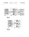
- FIG. 1shows a system architecture for a multimedia device with a digital signal processing subsystem
- FIG. 2is shows a modular, scalable bus architecture according to the present invention
- FIG. 3is a functional block diagram of a first system embodiment that employs a bus architecture according to the present invention
- FIG. 4is a functional block diagram of a second system embodiment that employs a bus architecture according to the present invention.
- FIG. 5is a functional block diagram of a transfer master
- FIG. 6shows an illustrative memory write-protection portion of a device port
- FIG. 7is a functional block diagram of a router
- FIG. 8is a functional block diagram of a data channel bridge
- FIG. 9is a functional block diagram of an address bus bridge.
- FIG. 2shows a modular, scalable, bus architecture that supports concurrent high-bandwidth memory connections for each processor element in the system, and that is suitable for systems employing one or more digital signal processors and hardware accelerators.
- systems employing this bus architecturemay be easily scaled and customized to specific applications. The customization can address various system design constraints such as power consumption, performance, and re-use of existing modules.
- the architecture as shown in FIG. 2includes three portions: a memory portion 202 , a data transfer portion (transfer master) 204 , and a processor portion 206 .
- Memory portion 202is an array of memory units and memory mapped devices each coupled to the transfer master 204 by address, data, and control lines.
- the memory unitspreferably receive enable, read, and write control signals on the control lines, and respond in the standard manner.
- an enabled read operationcauses a memory unit to provide read data on the data lines.
- Read datais a set of signals that represent data retrieved from a memory location identified by the address signals.
- An enabled write operationcauses a memory module to store write data from the data lines in a memory location identified by the address signals. When the memory unit is not enabled, it takes no action.
- the memory unitspreferably consist of memory modules that have a common data width, preferably eight bits. Memory modules may be combined to form a “memory unit” where greater data widths are needed. The depth (number of storage locations) of the memory modules may vary between memory units. Each memory module preferably has a read port and a write port. Such a memory module can be implemented using a time-multiplexed single port memory. In other words, a memory which supports only one access at a time (a single port memory) can be clocked at twice the system clock and the accesses may be alternated between read and write operations. This is not a fundamental requirement of the architecture, and other embodiments employing single port memory modules and multi-port memory modules (memory modules which support multiple simultaneous read/write accesses) are also contemplated.
- the design of the memory modulesmay be determined independently of the design and arrangement of the data transfer portion 204 and the processor portion 206 .
- the transfer master 204preferably provides a standardized interface to which the memory modules may be coupled.
- Transfer master 204independently coordinates all inter-processor, inter-memory, and processor-memory communications.
- the structure of transfer master 204is discussed further below. However, it is noted here that the transfer master operates to organize the memory portion 202 into a shared memory which is wholly accessible (subject to programmable memory protection settings) to each processor unit.
- the processor unitsare each assigned ownership of a memory module.
- the memory modulecorresponds to a memory “page” (the size of each memory page is individually configurable). Access to memory pages owned by other processor units may be obtained by a given processor unit by setting the given processor unit's page pointer to point to the desired memory page.
- Memory addresses from a processor unitare treated as offset addresses from the address indicated by the processor unit's page pointer.
- Processor portion 206is an array of two or more processor units.
- the processor unitsmay be of various types such as a digital signal processor (DSP), a hardware accelerator (denoted “ACCEL” in the figures), a microcontroller unit (MCU), or an interface port to a system including any one of these.
- the transfer master 204preferably provides a standardized interface for coupling to the processor units.
- the processor unitsare coupled to the transfer master 204 by control lines, address lines, and data lines.
- the control linespreferably carry control signals such as Enable, Read, Write, Ready, and Interrupt.
- the processor unitspreferably provide the Enable, Read, and Write signals on the control lines, and receive the Ready and Interrupt signals.
- the control linesmay further carry transfer request signals from the processor units. These signals preferably include a transfer type, a transfer source, a transfer target, and a transfer size.
- a processor unitTo send data, a processor unit provides an address on the address lines, data on the data lines, and a transfer request on the control lines. The processor unit then asserts the Enable signal and the Write signal. The transfer master 204 transfers the data and asserts the Ready signal when it is ready for any subsequent data transfer operation. To receive data, a processor unit provides an address on the address lines and a transfer request on the control lines, asserts the Enable signal and the Read signal, and waits for an assertion of the Ready signal. The transfer master 204 retrieves the data and provides the data on the data lines, then asserts the Ready signal to indicate that the data is available. It is noted that the design of the processor units is determined independently of the design and arrangement of other processor units, the transfer master 204 , and the memory portion 202 . This is achieved through the use of a standardized processor interface provided by the transfer master 204 .
- FIG. 3shows a functional block diagram of one system embodiment that illustratively employs the present architecture.
- the systemincludes a microcontroller bus 102 which couples a microcontroller unit 104 to a microcontroller memory 106 and a bus bridge 308 .
- Bus bridge 308couples microcontroller bus 102 to a peripheral bus 310 , whereby the microcontroller 104 can access peripheral devices 312 and external memory 314 .
- Peripheral devices 312preferably provide an interface to the external environment whereby the microcontroller unit 104 can obtain input data and instructions and can provide output results.
- External memory 314preferably provides long term program and data storage when the system is powered down.
- a transfer master 204is coupled to the MCU port 316 and various special purpose processors such as a hardware accelerator 318 and a digital signal processor (DSP) 320 .
- DSPdigital signal processor
- Transfer master 204coordinates data transfers between the array of processors (including the microcontroller 104 via MCU port 316 ) and a logically-mapped shared memory 322 via data path 324 .
- Transfer master 204handles memory-to-memory, memory-to-processor, processor-to-memory, and processor-to-processor data transfers.
- Shared memory block 322represents the logical map of the memory address space as it appears to the processors.
- the shared memoryis preferably used to store program instructions (PMEM) and data (DMEM) for each of the processors, as well as mailbox information (for inter-processor communication), memory configuration information, and interrupt queue information.
- the memoryis divided into pages, with ownership, reading, writing, and execution privileges of each processor for each page being assigned in the memory configuration information.
- the transfer master 204allows every processor to read or write from any of the memory pages.
- Each processing unitsupplies a page pointer to the transfer master 204 as part of the transfer request information (the transfer source or target).
- the individual processor unitsgain access to the various memory pages by setting their page pointers accordingly.
- shared memory 322 and data path 324are conceptual representations provided for explanatory purposes, and are not necessarily present as physical circuits in an implemented system. Rather, the shared memory 322 is preferably implemented partially as registers (for memory configuration and the interrupt queue) and partially as separate, strategically placed memory modules of various sizes.
- Data path 324preferably comprises a plurality of address and data busses which are routed to corresponding memory modules, registers, and memory-mapped devices.
- the program instructions for each of the processor unitsare kept in memory array 202 .
- the program instructionsmay be kept in dedicated memories coupled directly to the processor units.
- Other embodimentsare also contemplated that employ some combination of this.
- FIG. 4shows a functional block diagram of a second system embodiment that illustratively employs the present architecture.
- the microcontroller 104is coupled directly to the transfer master 204 .
- the microcontroller memory, external memory, and peripheralsare coupled to the transfer master 204 and logically mapped into the shared memory 322 .
- FIG. 5shows an exemplary embodiment of transfer master 204 .
- Transfer master 204preferably comprises port buffer logic 402 for latching address, write data, and control signals from the processors, and for driving control and read data signals to the processors.
- the port buffer logic 402may additionally provide timing synchronization, control signal generation, and multiplexing/de-multiplexing functions, as necessary.
- Port buffer logic 402couples the address and data signals from processors 104 (possibly via MCU port 316 ), 318 , and 320 , to router 404 , and also receives control signals from memory management unit (MMU) 406 .
- the memory management unit 406provides the control signals to port logic 402 and a conflict-free access pattern 410 to router 404 in response to transfer requests stored in one or more request queues 408 .
- Processor units 104 , 318 , 320place transfer requests in the queues 408 via transfer request lines 412 .
- Request queues 408preferably include a single transfer queue, a block transfer queue, and a mailbox message queue.
- Single transfersare transfers of a single word. They are intended for fast transfers between a processing unit and the corresponding memory module, and are accordingly assigned highest priority.
- Block transfersare transfers of a block of memory. Block transfers are intended primarily for direct memory access (DMA)-type transfers of data between memory modules. The priority of these transfers is user-configurable, and these transfers can be interrupted by transfers having a higher priority (such as single transfers).
- Mailbox messagesnotify a target processing unit of the need to carry out a transfer of information from a specified address. Mailbox messages are intended for transfers of information between processing units. The target devices are notified of the existence of the message via an interrupt, and the transfer is carried out in a manner determined by the target processing unit.
- the MMU 406responds to the contents of the request queues by establishing an access pattern that provides for the highest priority transfer requests and as many other transfer requests as possible without creating an access conflict.
- This conflict-free access pattern 410is provided to the router 404 .
- the pattern signal 410sets switches in the router to establish connections between the processing units and memory modules 420 - 428 that will allow for the transfer requests to occur. It is noted that configuration and status registers for the transfer master 204 may be accessible as one of the memory mapped devices 428 .
- the MMU 406may provide control signals to the port logic 402 to delay accesses that cannot occur in the context of the chosen access pattern 410 .
- the MMUpreferably maintains a distributed memory configuration table that tracks such things as read, write, and execute permissions of each processor for each memory page.
- the MMU 406provides control signals to port logic 402 to enforce memory protection.
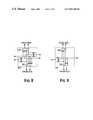
- FIG. 6shows one way to implement memory write protection.
- a port 402includes a configurable acceptance table 501 and a pass gate 502 .
- MMUprocesses the contents of the request queues 408 and generates a transfer target identifier for each of the ports 402 .
- the transfer targetis provided to acceptance table 501 , which responsively asserts or de-asserts an accept signal.
- a pass gate 502logically ANDs the accept signal with the write request signal from the processing unit.
- the output of pass gate 502is a write enable signal that is suppressed if the transfer target is not one of the allowable write-transfer targets as specified by the acceptance table 501 . It is noted that a status bit may be set in one of the transfer master status registers to indicate the detection of an attempted illegal write.
- transfer master 204also preferably includes an interrupt control unit (ICU) which provides interrupt signals 414 to each of the processors.
- the interruptsmay be used for block transfers, mailbox messages, memory protection violations, etc.
- Processorscan initiate block transfers of data by writing a block transfer request to the block transfer queue.
- the MMU 406will then handle the address generation and routing for block transfers of data.
- the ICUcan be configured to assert an interrupt to the block transfer requestor to notify the requester of the completion of the transfer.
- Processorscan communicate by writing mailbox messages to other processors. After the MMU 406 determines that a mailbox message is present in the request queue, the ICU asserts an interrupt to notify the addressee of the message's existence. If the MMU 406 detects the DSP writing to the hardware accelerator's memory page without programmed write permission, the ICU may assert an interrupt to alert one of the processors of the memory protection, violation.
- MMU 406will have a relatively uncomplicated (and therefore fast) implementation much simpler than a typical general purpose memory controller for a shared memory system.
- Each processor's accesses to its own memory pagesare expected to incur no latency (i.e. read data is received on the first clock cycle subsequent to the clock cycle in which the address is provided), and only a minimal latency is expected to be incurred by accesses to other memory pages.
- FIG. 7shows a functional block diagram of an exemplary embodiment of router 404 .
- Router 404couples port logic 402 and direct memory access (DMA) controller 504 to memory modules 420 - 424 , external memory 426 , and memory mapped devices 428 .
- DMA controller 504is the portion of MMU 406 that conducts block transfers. It may be configured to generate addresses to read data from the source memory into a cache, and then to generate addresses to write data from the cache into the target memory.
- DMA controller 504preferably includes logic to handle word-size and word-alignment issues that can crop up when data is transferred in blocks.
- Router 404includes bi-directional data channel bridges 506 and unidirectional address bus bridges 508 .
- Router 404preferably divides the data busses into data channels of uniform width, e.g. 8-bits.
- the channel bit-widthis chosen to be a common integer factor of popular data bus bit-widths.
- Each data channelis coupled by a channel bridge 506 to a cross-bus data channel having the same bit-width.
- the address bussesare be similarly coupled via address bridges 508 to an address cross-bus.
- the cross-buspreferably has a ring structure, i.e. the channel bridges at the bottom of FIG. 7 are coupled via the dashed arrows to the corresponding bridges at the top of FIG. 7 .
- this embodimentshows three processing units and the data channels in this embodiment are described as having eight bit data path widths, these numbers are not intended to be limiting in any way. Rather, the bus architecture is intended to be general, and is capable of being implemented in a wide variety of embodiments. Features of such embodiments may include having more channels, more processors, and perhaps larger data path widths.
- the memory modulesmay be multi-ported, in which case more data busses are expected to be associated with each memory module.
- the read and write data pathspreferably have eight-bit widths, as do the data cross-paths.
- Each of the bi-directional data pathsare coupled to both directions of a cross-bus data channel by a bi-directional channel bridge 506
- each of the address pathsare coupled to both directions of an address cross-bus by a unidirectional address bus bridge 508 .
- the bridgesinclude buffers 602 for the cross-bus signals, and multiplexers 604 for each of the outgoing signals.
- a multiplexer 604 for an outgoing signalselects from incoming signals from the other three directions. In the case of the unidirectional bridge 504 , one of the incoming signals and one of the outgoing signals is removed. Consequently, the hardware is simplified and a two-input multiplexer 606 can be used. Control signals are provided from MMU 406 to the multiplexers 604 , 606 to direct the bus signals as desired.
- the buffers 602may perform a latching function. In other words, the buffers latch bit signals from input bit lines, and provide the latched bit signals on the output lines on a subsequent clock cycle. This allows the cross-path to be divided into shorter segments that can carry different bit signals concurrently. However, propagation between segments accrues a latency of one clock-cycle per segment. Consequently, it may be desirable to provide some bridges with non-latching buffers to keep the number of segments to a minimum. In this manner, a trade-off between throughput and cross-path latency may be achieved.
- address pathsdo not necessarily have uniform bit widths, and consequently, the bit width of the address cross-path must be adequate to support the maximum address path bit width. At those junctions where the address path bit width is less than the cross-path bit width, not all of the cross-bus address bit lines are coupled to the memory address bit lines.
- Multimedia systemstypically have audio, video, administrative, and real-time tasks.
- the processor unitsgenerally need to trade data back and forth to carry out all these tasks. However, it is noted that these data exchanges are not random or unstructured. Rather, the tasks performed by multimedia systems tend to be well-defined tasks involving known memory sizes and predictable communications paths. If the memory modules are configured to support simultaneous reads and writes, memory access collisions can often be minimized by the software programmer.
- the microcontroller unitis expected to communicate primarily with the DSP, and only rarely directly with the hardware accelerator.
- the hardware acceleratoris expected to communicate primarily with the DSP and only rarely with the microcontroller unit.
- the DSPis located on the cross-bus between the microcontroller unit and the accelerator and adjacent to both. This allows the processor units to realize a minimal latency when accessing “local” (their own) or “adjacent” (owned by the neighboring processor unit) memory pages.
- Microcontroller 104may be executing an operating system that instructs a memory mapped device to downloads an encoded video macroblock to the DSP memory 422 four bytes at a time.
- the microcontroller 104then writes a “Start Viterbi Algorithm” mailbox message to the DSP's mailbox (the message may be written to the MCU memory 420 , and a mailbox message transfer request sent to MMU 406 ).
- the DSP 320receives the message and decodes the video macroblock using the Viterbi algorithm, writing the results to the hardware accelerator's memory 424 .
- the DSP 320sends a message to the accelerator's mailbox to start the inverse discrete cosine transform of the decoded macroblock.
- the accelerator 318performs the IDCT, writing pixel results to the a video buffer in the memory mapped devices 428 .
- the accelerator 318sends a message to notify the MCU 104 of the completed transfer of the decoded video block to the video buffer.
- the disclosed architectureresolves these issues and further provides a logically-mapped shared memory.
- the disclosed architecturesimplifies many programming and system design issues.
- the disclosed architecturealso benefits in terms of scalability from the use of uniform-width data channels and the modularized memory.
- the use of request queuesmay provide for a way to eliminate critical path issues from the transfer master design, and thereby enable the architecture to “ride the technology curve”, i.e. allow systems employing this architecture to be implemented using the newest integrated circuit technology with little or no system re-design.
- various system implementationsmay be designed with various numbers of processing units and/or various transfer master routing efficiencies (i.e. various effective bandwidths to memory) to provide a customer with a customized cost/performance tradeoff.
- various transfer master routing efficienciesi.e. various effective bandwidths to memory
Landscapes
- Engineering & Computer Science (AREA)
- Computer Hardware Design (AREA)
- Theoretical Computer Science (AREA)
- Multimedia (AREA)
- Signal Processing (AREA)
- Physics & Mathematics (AREA)
- General Physics & Mathematics (AREA)
- Computing Systems (AREA)
- General Engineering & Computer Science (AREA)
- Bus Control (AREA)
- Multi Processors (AREA)
Abstract
Description
Claims (25)
Priority Applications (1)
| Application Number | Priority Date | Filing Date | Title |
|---|---|---|---|
| US09/343,872US6915369B1 (en) | 1999-02-25 | 1999-06-30 | Modular and scalable system bus structure |
Applications Claiming Priority (2)
| Application Number | Priority Date | Filing Date | Title |
|---|---|---|---|
| US09/257,840US6275891B1 (en) | 1999-02-25 | 1999-02-25 | Modular and scalable system for signal and multimedia processing |
| US09/343,872US6915369B1 (en) | 1999-02-25 | 1999-06-30 | Modular and scalable system bus structure |
Related Parent Applications (1)
| Application Number | Title | Priority Date | Filing Date |
|---|---|---|---|
| US09/257,840Continuation-In-PartUS6275891B1 (en) | 1999-02-25 | 1999-02-25 | Modular and scalable system for signal and multimedia processing |
Publications (1)
| Publication Number | Publication Date |
|---|---|
| US6915369B1true US6915369B1 (en) | 2005-07-05 |
Family
ID=22977981
Family Applications (2)
| Application Number | Title | Priority Date | Filing Date |
|---|---|---|---|
| US09/257,840Expired - LifetimeUS6275891B1 (en) | 1999-02-25 | 1999-02-25 | Modular and scalable system for signal and multimedia processing |
| US09/343,872Expired - Fee RelatedUS6915369B1 (en) | 1999-02-25 | 1999-06-30 | Modular and scalable system bus structure |
Family Applications Before (1)
| Application Number | Title | Priority Date | Filing Date |
|---|---|---|---|
| US09/257,840Expired - LifetimeUS6275891B1 (en) | 1999-02-25 | 1999-02-25 | Modular and scalable system for signal and multimedia processing |
Country Status (1)
| Country | Link |
|---|---|
| US (2) | US6275891B1 (en) |
Cited By (13)
| Publication number | Priority date | Publication date | Assignee | Title |
|---|---|---|---|---|
| US20050071210A1 (en)* | 2003-09-25 | 2005-03-31 | Gish David W. | Method, system, and apparatus for an adaptive weighted arbiter |
| US20060230213A1 (en)* | 2005-03-29 | 2006-10-12 | Via Technologies, Inc. | Digital signal system with accelerators and method for operating the same |
| US20090083471A1 (en)* | 2007-09-20 | 2009-03-26 | Bradly George Frey | Method and apparatus for providing accelerator support in a bus protocol |
| CZ300812B6 (en)* | 2007-12-04 | 2009-08-12 | Cesnet | Modular programmable platform for high-speed hardware processing of packets |
| GB2459331A (en)* | 2008-04-24 | 2009-10-28 | Icera Inc | Serial interface between integrated circuits using a bundle of independent direct memory access requests |
| US20090328183A1 (en)* | 2006-06-27 | 2009-12-31 | Waterfall Solutions Ltd. | One way secure link |
| US20100278339A1 (en)* | 2006-12-12 | 2010-11-04 | Human Interface Security Ltd | Encryption- and decryption-enabled interfaces |
| US20130097280A1 (en)* | 2004-03-18 | 2013-04-18 | Nokia Coporation | System and associated terminal, method and computer program product for uploading content |
| US20140244780A1 (en)* | 2007-01-16 | 2014-08-28 | Waterfall Security Solutions Ltd. | Secure Archive |
| US9369446B2 (en) | 2014-10-19 | 2016-06-14 | Waterfall Security Solutions Ltd. | Secure remote desktop |
| US9419975B2 (en) | 2013-04-22 | 2016-08-16 | Waterfall Security Solutions Ltd. | Bi-directional communication over a one-way link |
| US9635037B2 (en) | 2012-09-06 | 2017-04-25 | Waterfall Security Solutions Ltd. | Remote control of secure installations |
| US10356226B2 (en) | 2016-02-14 | 2019-07-16 | Waaterfall Security Solutions Ltd. | Secure connection with protected facilities |
Families Citing this family (14)
| Publication number | Priority date | Publication date | Assignee | Title |
|---|---|---|---|---|
| US6275891B1 (en)* | 1999-02-25 | 2001-08-14 | Lsi Logic Corporation | Modular and scalable system for signal and multimedia processing |
| US6754509B1 (en)* | 1999-12-30 | 2004-06-22 | Qualcomm, Incorporated | Mobile communication device having dual micro processor architecture with shared digital signal processor and shared memory |
| WO2001050624A1 (en)* | 1999-12-30 | 2001-07-12 | Morphics Technology, Inc. | Method and apparatus to support multi standard, multi service base-stations for wireless voice and data networks |
| US6609188B1 (en)* | 2000-03-31 | 2003-08-19 | Intel Corporation | Data flow processor |
| US7649943B2 (en)* | 2000-04-21 | 2010-01-19 | Microsoft Corporation | Interface and related methods facilitating motion compensation in media processing |
| US6940912B2 (en)* | 2000-04-21 | 2005-09-06 | Microsoft Corporation | Dynamically adaptive multimedia application program interface and related methods |
| US7634011B2 (en)* | 2000-04-21 | 2009-12-15 | Microsoft Corporation | Application program interface (API) facilitating decoder control of accelerator resources |
| US6891893B2 (en)* | 2000-04-21 | 2005-05-10 | Microsoft Corp. | Extensible multimedia application program interface and related methods |
| DE10157874B4 (en)* | 2001-11-26 | 2005-07-14 | Infineon Technologies Ag | Device for supplying control signals to memory units and adapted memory unit |
| US7073048B2 (en)* | 2002-02-04 | 2006-07-04 | Silicon Lease, L.L.C. | Cascaded microcomputer array and method |
| US7236525B2 (en)* | 2003-05-22 | 2007-06-26 | Lsi Corporation | Reconfigurable computing based multi-standard video codec |
| US7714870B2 (en) | 2003-06-23 | 2010-05-11 | Intel Corporation | Apparatus and method for selectable hardware accelerators in a data driven architecture |
| US20130039431A1 (en)* | 2011-08-12 | 2013-02-14 | Electronics And Telecommunications Research Institute | Power-scalable encoding/decoding apparatus and method |
| JP2013196167A (en)* | 2012-03-16 | 2013-09-30 | Toshiba Corp | Information processor |
Citations (14)
| Publication number | Priority date | Publication date | Assignee | Title |
|---|---|---|---|---|
| US5581767A (en)* | 1993-06-16 | 1996-12-03 | Nippon Sheet Glass Co., Ltd. | Bus structure for multiprocessor system having separated processor section and control/memory section |
| US5815457A (en)* | 1995-06-26 | 1998-09-29 | Sgs-Thomson Microelectronics S.R.L. | Bit line selection decoder for an electronic memory |
| US5890003A (en)* | 1988-12-09 | 1999-03-30 | Tandem Computers Incorporated | Interrupts between asynchronously operating CPUs in fault tolerant computer system |
| US5987576A (en)* | 1997-02-27 | 1999-11-16 | Hewlett-Packard Company | Method and apparatus for generating and distributing clock signals with minimal skew |
| US6092141A (en)* | 1996-09-26 | 2000-07-18 | Vlsi Technology, Inc. | Selective data read-ahead in bus-to-bus bridge architecture |
| US6125429A (en)* | 1998-03-12 | 2000-09-26 | Compaq Computer Corporation | Cache memory exchange optimized memory organization for a computer system |
| US6141718A (en)* | 1998-06-15 | 2000-10-31 | Sun Microsystems, Inc. | Processor bridge with dissimilar data registers which is operable to disregard data differences for dissimilar data direct memory accesses |
| US6148356A (en)* | 1995-12-27 | 2000-11-14 | Intel Corporation | Scalable computer system |
| US6263393B1 (en)* | 1998-02-17 | 2001-07-17 | Nec Corporation | Bus switch for realizing bus transactions across two or more buses |
| US6275891B1 (en)* | 1999-02-25 | 2001-08-14 | Lsi Logic Corporation | Modular and scalable system for signal and multimedia processing |
| US6298384B1 (en)* | 1997-11-10 | 2001-10-02 | Fujitsu Limited | Data processing apparatus for transferring data over unidirectional bus |
| US20020002662A1 (en)* | 1998-07-13 | 2002-01-03 | Olarig Sompong Paul | Method and apparatus for supporting heterogeneous memory in computer systems |
| US20020091905A1 (en)* | 1999-01-29 | 2002-07-11 | Interactive Silicon, Incorporated, | Parallel compression and decompression system and method having multiple parallel compression and decompression engines |
| US20020161965A1 (en)* | 1997-07-01 | 2002-10-31 | Kevin J. Ryan | Pipelined packet-oriented memory system having a unidirectional command and address bus and a bidirectional data bus |
Family Cites Families (9)
| Publication number | Priority date | Publication date | Assignee | Title |
|---|---|---|---|---|
| US5152000A (en)* | 1983-05-31 | 1992-09-29 | Thinking Machines Corporation | Array communications arrangement for parallel processor |
| US5249301A (en)* | 1988-10-25 | 1993-09-28 | Bull S.A | Processing communication system having a plurality of memories and processors coupled through at least one feedback shift register provided from ring configured input stations |
| CA2036688C (en)* | 1990-02-28 | 1995-01-03 | Lee W. Tower | Multiple cluster signal processor |
| JP3479538B2 (en)* | 1991-12-26 | 2003-12-15 | テキサス インスツルメンツ インコーポレイテツド | Method of manufacturing semiconductor integrated circuit |
| JPH0792790B2 (en)* | 1992-11-18 | 1995-10-09 | 野木 達夫 | Vector parallel computer |
| US6116768A (en)* | 1993-11-30 | 2000-09-12 | Texas Instruments Incorporated | Three input arithmetic logic unit with barrel rotator |
| US5535406A (en)* | 1993-12-29 | 1996-07-09 | Kolchinsky; Alexander | Virtual processor module including a reconfigurable programmable matrix |
| JPH1078934A (en)* | 1996-07-01 | 1998-03-24 | Sun Microsyst Inc | Multi-size bus connection system for packet switching computer system |
| US5842034A (en)* | 1996-12-20 | 1998-11-24 | Raytheon Company | Two dimensional crossbar mesh for multi-processor interconnect |
- 1999
- 1999-02-25USUS09/257,840patent/US6275891B1/ennot_activeExpired - Lifetime
- 1999-06-30USUS09/343,872patent/US6915369B1/ennot_activeExpired - Fee Related
Patent Citations (14)
| Publication number | Priority date | Publication date | Assignee | Title |
|---|---|---|---|---|
| US5890003A (en)* | 1988-12-09 | 1999-03-30 | Tandem Computers Incorporated | Interrupts between asynchronously operating CPUs in fault tolerant computer system |
| US5581767A (en)* | 1993-06-16 | 1996-12-03 | Nippon Sheet Glass Co., Ltd. | Bus structure for multiprocessor system having separated processor section and control/memory section |
| US5815457A (en)* | 1995-06-26 | 1998-09-29 | Sgs-Thomson Microelectronics S.R.L. | Bit line selection decoder for an electronic memory |
| US6148356A (en)* | 1995-12-27 | 2000-11-14 | Intel Corporation | Scalable computer system |
| US6092141A (en)* | 1996-09-26 | 2000-07-18 | Vlsi Technology, Inc. | Selective data read-ahead in bus-to-bus bridge architecture |
| US5987576A (en)* | 1997-02-27 | 1999-11-16 | Hewlett-Packard Company | Method and apparatus for generating and distributing clock signals with minimal skew |
| US20020161965A1 (en)* | 1997-07-01 | 2002-10-31 | Kevin J. Ryan | Pipelined packet-oriented memory system having a unidirectional command and address bus and a bidirectional data bus |
| US6298384B1 (en)* | 1997-11-10 | 2001-10-02 | Fujitsu Limited | Data processing apparatus for transferring data over unidirectional bus |
| US6263393B1 (en)* | 1998-02-17 | 2001-07-17 | Nec Corporation | Bus switch for realizing bus transactions across two or more buses |
| US6125429A (en)* | 1998-03-12 | 2000-09-26 | Compaq Computer Corporation | Cache memory exchange optimized memory organization for a computer system |
| US6141718A (en)* | 1998-06-15 | 2000-10-31 | Sun Microsystems, Inc. | Processor bridge with dissimilar data registers which is operable to disregard data differences for dissimilar data direct memory accesses |
| US20020002662A1 (en)* | 1998-07-13 | 2002-01-03 | Olarig Sompong Paul | Method and apparatus for supporting heterogeneous memory in computer systems |
| US20020091905A1 (en)* | 1999-01-29 | 2002-07-11 | Interactive Silicon, Incorporated, | Parallel compression and decompression system and method having multiple parallel compression and decompression engines |
| US6275891B1 (en)* | 1999-02-25 | 2001-08-14 | Lsi Logic Corporation | Modular and scalable system for signal and multimedia processing |
Cited By (23)
| Publication number | Priority date | Publication date | Assignee | Title |
|---|---|---|---|---|
| US7350003B2 (en)* | 2003-09-25 | 2008-03-25 | Intel Corporation | Method, system, and apparatus for an adaptive weighted arbiter |
| US20050071210A1 (en)* | 2003-09-25 | 2005-03-31 | Gish David W. | Method, system, and apparatus for an adaptive weighted arbiter |
| US20130097280A1 (en)* | 2004-03-18 | 2013-04-18 | Nokia Coporation | System and associated terminal, method and computer program product for uploading content |
| US20060230213A1 (en)* | 2005-03-29 | 2006-10-12 | Via Technologies, Inc. | Digital signal system with accelerators and method for operating the same |
| US9762536B2 (en) | 2006-06-27 | 2017-09-12 | Waterfall Security Solutions Ltd. | One way secure link |
| US20090328183A1 (en)* | 2006-06-27 | 2009-12-31 | Waterfall Solutions Ltd. | One way secure link |
| US20100278339A1 (en)* | 2006-12-12 | 2010-11-04 | Human Interface Security Ltd | Encryption- and decryption-enabled interfaces |
| US9268957B2 (en) | 2006-12-12 | 2016-02-23 | Waterfall Security Solutions Ltd. | Encryption-and decryption-enabled interfaces |
| US20150326546A1 (en)* | 2007-01-16 | 2015-11-12 | Waterfall Security Solutions Ltd. | Secure Archive |
| US9519616B2 (en)* | 2007-01-16 | 2016-12-13 | Waterfall Security Solution Ltd. | Secure archive |
| US20140244780A1 (en)* | 2007-01-16 | 2014-08-28 | Waterfall Security Solutions Ltd. | Secure Archive |
| US9116857B2 (en)* | 2007-01-16 | 2015-08-25 | Waterfall Security Solutions Ltd. | Secure archive |
| US7827343B2 (en)* | 2007-09-20 | 2010-11-02 | International Business Machines Corporation | Method and apparatus for providing accelerator support in a bus protocol |
| US20090083471A1 (en)* | 2007-09-20 | 2009-03-26 | Bradly George Frey | Method and apparatus for providing accelerator support in a bus protocol |
| CZ300812B6 (en)* | 2007-12-04 | 2009-08-12 | Cesnet | Modular programmable platform for high-speed hardware processing of packets |
| GB2459331A (en)* | 2008-04-24 | 2009-10-28 | Icera Inc | Serial interface between integrated circuits using a bundle of independent direct memory access requests |
| US8275921B2 (en) | 2008-04-24 | 2012-09-25 | Icera Inc. | Accessing data |
| GB2459331B (en)* | 2008-04-24 | 2012-02-15 | Icera Inc | Direct Memory Access (DMA) via a serial link |
| US20090271555A1 (en)* | 2008-04-24 | 2009-10-29 | Andy Bond | Accessing data |
| US9635037B2 (en) | 2012-09-06 | 2017-04-25 | Waterfall Security Solutions Ltd. | Remote control of secure installations |
| US9419975B2 (en) | 2013-04-22 | 2016-08-16 | Waterfall Security Solutions Ltd. | Bi-directional communication over a one-way link |
| US9369446B2 (en) | 2014-10-19 | 2016-06-14 | Waterfall Security Solutions Ltd. | Secure remote desktop |
| US10356226B2 (en) | 2016-02-14 | 2019-07-16 | Waaterfall Security Solutions Ltd. | Secure connection with protected facilities |
Also Published As
| Publication number | Publication date |
|---|---|
| US6275891B1 (en) | 2001-08-14 |
Similar Documents
| Publication | Publication Date | Title |
|---|---|---|
| US6915369B1 (en) | Modular and scalable system bus structure | |
| US5655151A (en) | DMA controller having a plurality of DMA channels each having multiple register sets storing different information controlling respective data transfer | |
| US6295553B1 (en) | Method and apparatus for prioritizing delivery of data transfer requests | |
| US6910108B2 (en) | Hardware support for partitioning a multiprocessor system to allow distinct operating systems | |
| KR100962769B1 (en) | Supercharge Message Exchange | |
| US20060004976A1 (en) | Shared memory architecture | |
| US20020004886A1 (en) | Multiprocessing computer system employing a cluster protection mechanism | |
| JPH1097513A (en) | Node in multiprocessor computer system and multiprocessor computer system | |
| EP1047994A2 (en) | Intelligent data bus interface using multi-port memory | |
| KR100951856B1 (en) | SOC system for multimedia system | |
| EP1233329B1 (en) | Shared component clock protrction for multicore DSP device | |
| CA2478570A1 (en) | Data processing apparatus and system and method for controlling memory access | |
| US20120311266A1 (en) | Multiprocessor and image processing system using the same | |
| US6892266B2 (en) | Multicore DSP device having coupled subsystem memory buses for global DMA access | |
| KR100630071B1 (en) | High speed data transmission method using DM in multiprocessor environment and apparatus therefor | |
| US7058740B2 (en) | Effective bus utilization using multiple buses and multiple bus controllers | |
| US7020733B2 (en) | Data bus system and method for performing cross-access between buses | |
| US7006521B2 (en) | External bus arbitration technique for multicore DSP device | |
| CN100527104C (en) | HDD controller and system equipped with the same | |
| US20030009532A1 (en) | Multiprocessor system having a shared main memory | |
| JP2831083B2 (en) | Multiprocessor system and interrupt controller | |
| US5666556A (en) | Method and apparatus for redirecting register access requests wherein the register set is separate from a central processing unit | |
| JP4928683B2 (en) | Data processing device | |
| EP0661641A2 (en) | A computer system | |
| JPH05210481A (en) | Direct access type video bus |
Legal Events
| Date | Code | Title | Description |
|---|---|---|---|
| AS | Assignment | Owner name:LSI LOGIC CPOPATION, CALIFORNIA Free format text:ASSIGNMENT OF ASSIGNORS INTEREST;ASSIGNORS:DAO, TUAN Q.;NG, PIUS;LOOK, PAUL;REEL/FRAME:010077/0858 Effective date:19990625 | |
| FEPP | Fee payment procedure | Free format text:PAYOR NUMBER ASSIGNED (ORIGINAL EVENT CODE: ASPN); ENTITY STATUS OF PATENT OWNER: LARGE ENTITY | |
| FPAY | Fee payment | Year of fee payment:4 | |
| FPAY | Fee payment | Year of fee payment:8 | |
| AS | Assignment | Owner name:DEUTSCHE BANK AG NEW YORK BRANCH, AS COLLATERAL AG Free format text:PATENT SECURITY AGREEMENT;ASSIGNORS:LSI CORPORATION;AGERE SYSTEMS LLC;REEL/FRAME:032856/0031 Effective date:20140506 | |
| AS | Assignment | Owner name:AVAGO TECHNOLOGIES GENERAL IP (SINGAPORE) PTE. LTD Free format text:ASSIGNMENT OF ASSIGNORS INTEREST;ASSIGNOR:LSI CORPORATION;REEL/FRAME:035390/0388 Effective date:20140814 | |
| AS | Assignment | Owner name:LSI CORPORATION, CALIFORNIA Free format text:TERMINATION AND RELEASE OF SECURITY INTEREST IN PATENT RIGHTS (RELEASES RF 032856-0031);ASSIGNOR:DEUTSCHE BANK AG NEW YORK BRANCH, AS COLLATERAL AGENT;REEL/FRAME:037684/0039 Effective date:20160201 Owner name:AGERE SYSTEMS LLC, PENNSYLVANIA Free format text:TERMINATION AND RELEASE OF SECURITY INTEREST IN PATENT RIGHTS (RELEASES RF 032856-0031);ASSIGNOR:DEUTSCHE BANK AG NEW YORK BRANCH, AS COLLATERAL AGENT;REEL/FRAME:037684/0039 Effective date:20160201 | |
| AS | Assignment | Owner name:BANK OF AMERICA, N.A., AS COLLATERAL AGENT, NORTH CAROLINA Free format text:PATENT SECURITY AGREEMENT;ASSIGNOR:AVAGO TECHNOLOGIES GENERAL IP (SINGAPORE) PTE. LTD.;REEL/FRAME:037808/0001 Effective date:20160201 Owner name:BANK OF AMERICA, N.A., AS COLLATERAL AGENT, NORTH Free format text:PATENT SECURITY AGREEMENT;ASSIGNOR:AVAGO TECHNOLOGIES GENERAL IP (SINGAPORE) PTE. LTD.;REEL/FRAME:037808/0001 Effective date:20160201 | |
| AS | Assignment | Owner name:AVAGO TECHNOLOGIES GENERAL IP (SINGAPORE) PTE. LTD., SINGAPORE Free format text:TERMINATION AND RELEASE OF SECURITY INTEREST IN PATENTS;ASSIGNOR:BANK OF AMERICA, N.A., AS COLLATERAL AGENT;REEL/FRAME:041710/0001 Effective date:20170119 Owner name:AVAGO TECHNOLOGIES GENERAL IP (SINGAPORE) PTE. LTD Free format text:TERMINATION AND RELEASE OF SECURITY INTEREST IN PATENTS;ASSIGNOR:BANK OF AMERICA, N.A., AS COLLATERAL AGENT;REEL/FRAME:041710/0001 Effective date:20170119 | |
| REMI | Maintenance fee reminder mailed | ||
| LAPS | Lapse for failure to pay maintenance fees | ||
| STCH | Information on status: patent discontinuation | Free format text:PATENT EXPIRED DUE TO NONPAYMENT OF MAINTENANCE FEES UNDER 37 CFR 1.362 | |
| FP | Lapsed due to failure to pay maintenance fee | Effective date:20170705 |