US6912680B1 - Memory system with dynamic timing correction - Google Patents
Memory system with dynamic timing correctionDownload PDFInfo
- Publication number
- US6912680B1 US6912680B1US08/798,227US79822797AUS6912680B1US 6912680 B1US6912680 B1US 6912680B1US 79822797 AUS79822797 AUS 79822797AUS 6912680 B1US6912680 B1US 6912680B1
- Authority
- US
- United States
- Prior art keywords
- clock signal
- data
- signal
- phase
- echo
- Prior art date
- Legal status (The legal status is an assumption and is not a legal conclusion. Google has not performed a legal analysis and makes no representation as to the accuracy of the status listed.)
- Expired - Fee Related, expires
Links
- 230000015654memoryEffects0.000titleclaimsabstractdescription118
- 230000004044responseEffects0.000claimsabstractdescription22
- 230000010363phase shiftEffects0.000claimsdescription10
- 230000003111delayed effectEffects0.000description18
- 230000001934delayEffects0.000description8
- 238000010586diagramMethods0.000description7
- 101000885321Homo sapiens Serine/threonine-protein kinase DCLK1Proteins0.000description5
- 102100039758Serine/threonine-protein kinase DCLK1Human genes0.000description5
- 230000001360synchronised effectEffects0.000description3
- 241000931526Acer campestreSpecies0.000description1
- 230000032683agingEffects0.000description1
- 238000004364calculation methodMethods0.000description1
- 238000013500data storageMethods0.000description1
- 230000006870functionEffects0.000description1
- 230000000977initiatory effectEffects0.000description1
- 238000012986modificationMethods0.000description1
- 230000004048modificationEffects0.000description1
- 230000007704transitionEffects0.000description1
Images


Classifications
- G—PHYSICS
- G11—INFORMATION STORAGE
- G11C—STATIC STORES
- G11C29/00—Checking stores for correct operation ; Subsequent repair; Testing stores during standby or offline operation
- G11C29/02—Detection or location of defective auxiliary circuits, e.g. defective refresh counters
- G11C29/028—Detection or location of defective auxiliary circuits, e.g. defective refresh counters with adaption or trimming of parameters
- G—PHYSICS
- G11—INFORMATION STORAGE
- G11C—STATIC STORES
- G11C29/00—Checking stores for correct operation ; Subsequent repair; Testing stores during standby or offline operation
- G11C29/04—Detection or location of defective memory elements, e.g. cell constructio details, timing of test signals
- G11C29/50—Marginal testing, e.g. race, voltage or current testing
- G11C29/50012—Marginal testing, e.g. race, voltage or current testing of timing
- G—PHYSICS
- G11—INFORMATION STORAGE
- G11C—STATIC STORES
- G11C7/00—Arrangements for writing information into, or reading information out from, a digital store
- G11C7/10—Input/output [I/O] data interface arrangements, e.g. I/O data control circuits, I/O data buffers
- G11C7/1051—Data output circuits, e.g. read-out amplifiers, data output buffers, data output registers, data output level conversion circuits
- G11C7/1063—Control signal output circuits, e.g. status or busy flags, feedback command signals
- G—PHYSICS
- G11—INFORMATION STORAGE
- G11C—STATIC STORES
- G11C7/00—Arrangements for writing information into, or reading information out from, a digital store
- G11C7/10—Input/output [I/O] data interface arrangements, e.g. I/O data control circuits, I/O data buffers
- G11C7/1051—Data output circuits, e.g. read-out amplifiers, data output buffers, data output registers, data output level conversion circuits
- G11C7/1066—Output synchronization
- G—PHYSICS
- G11—INFORMATION STORAGE
- G11C—STATIC STORES
- G11C7/00—Arrangements for writing information into, or reading information out from, a digital store
- G11C7/22—Read-write [R-W] timing or clocking circuits; Read-write [R-W] control signal generators or management
- G—PHYSICS
- G11—INFORMATION STORAGE
- G11C—STATIC STORES
- G11C7/00—Arrangements for writing information into, or reading information out from, a digital store
- G11C7/22—Read-write [R-W] timing or clocking circuits; Read-write [R-W] control signal generators or management
- G11C7/222—Clock generating, synchronizing or distributing circuits within memory device
- G—PHYSICS
- G11—INFORMATION STORAGE
- G11C—STATIC STORES
- G11C2207/00—Indexing scheme relating to arrangements for writing information into, or reading information out from, a digital store
- G11C2207/22—Control and timing of internal memory operations
- G11C2207/2254—Calibration
Definitions
- the present inventionrelates to memory systems and memory devices, and more particularly, to dynamic timing correction in memory systems and memory devices.
- Timing of operations in synchronous memory systemsmust tightly controlled if the memory system is to operate at optimum rates.
- timing of operations in synchronous systemsis controlled by a memory controller operating in synchronization with edges of the master clock signal.
- One problem that often occurs in such systemarises from differences in propagation times of signals between a memory controller and memory devices controlled by the memory controller. Such timing differences may prevent the memory system from operating at its optimum rate.
- the memory controllertypically accepts new data from a memory device at leading clock edges (i.e., transitions of the master clock signal from low to high). If one of the memory devices outputs data at the specified clock edge propagation delays from the memory device to the memory controller may cause the data to arrive later than the specified clock edge. Therefore, the memory device outputs data a short time before the leading edge to compensate for propagation of delays.
- One problem with such an approachis that propagation delays between the memory device and memory controller will depend upon the effective distance between the memory controller and the memory device, which depends upon the routing of signal lines connecting the memory controller to the memory device. Consequently, the data may still not arrive at the memory controller at the specified leading edge. Therefore, the memory controller must be prepared to accept the data for some time before and after the clock edge. To allow sufficient time to look for the data, the memory controller allots a larger than optimum time period for accepting the data. The overall speed of the memory system is limited correspondingly.
- a memory systemincludes a memory controller coupled to a plurality of memory devices.
- the memory controllerincludes a master clock generator that provides a master clock signal for controlling timing of operations within the memory system.
- the memory controlleralso includes a data clock generator that provides a data clock signal to control timing of data transfer to and from the memory devices.
- Each of the memory devicesincludes an echo clock generator that generates an echo clock signal in response to the master clock signal.
- the echo clock generatorincludes an output vernier that receives the master clock signal and produces a delayed data clock signal.
- the delayed data clock signaldrives an output register to provide output data to a data bus.
- Each memory devicealso transmits the delayed data clock signal to the memory controller as the echo clock signal.
- phase comparatorcompares the echo clock signal to the master clock signal to identify any phase shift of the echo clock signal relative to the master clock signal.
- control logic of the memory controllerprovides control data to the memory devices to adjust the vernier, thereby reducing the phase shift.
- the phase comparatoris formed from a plurality of phase detectors, where each phase detector has a first input driven by the echo clock signal.
- the phase detectorsalso have second inputs that receive phase-shifted versions of the maser clock signal.
- the memory controllerincludes a delay-locked loop driven by the master clock signal.
- the delay-locked loopincludes a multiple output variable delay circuit that outputs the phase-shifted versions of the master clock signal.
- the phase-shifted versions of the master clock signalinclude versions shifted relative to the master clock signal by 0, + ⁇ , ⁇ , +2 ⁇ , and ⁇ 2 ⁇ , where ⁇ is a selected increment greater than half of the finest adjustment available in the vernier.
- the use of a plurality of phase detectors driven by taps of a delay-locked loopallows the echo clock signal to be phase compared to the master clock signal in real time.
- the memory controllercan dynamically adjust timing of the memory devices to accommodate drift in routing delays of the memory system.
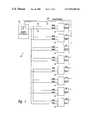
- FIG. 1is a block diagram of a memory system including a memory controller and eight memory devices.
- FIG. 2is a block diagram of one of the memory devices of FIG. 1 .
- FIG. 3is a block diagram of another embodiment of the memory system including a memory controller and eight memory devices where each memory device includes an echo clock generator coupled to the memory controller and the memory controller includes a phase comparing circuitry.
- FIG. 4is a block diagram of one of the memory devices of the memory system of FIG. 3 .
- FIG. 5is a block diagram of the master controller of FIG. 3 .
- FIG. 6is a block diagram of a computer system including the memory system of FIG. 3 .
- a memory system 40includes a memory controller 42 that controls eight memory devices 44 as directed by a logic control circuit 43 .
- the memory devices 44 and memory controller 42operate according to a packet protocol.
- the controller 42generates a control data packet containing control data CDAT for reading to or writing from one of the memory devices 44 or for initiating a memory event, such as reset or autorefresh.
- the data packetincludes fields identifying the memory device 44 to which the packet is directed, fields containing command data, and fields containing addressing information, such as row, column, bank, or register addresses.
- the memory controller 42transmits the control data packet to all of the memory devices 44 on a control data bus 46 that is coupled to control data inputs of all of the memory devices 44 .
- the memory controller 42In addition to the control data packets, the memory controller 42 also provides a master clock signal MCLK on a master clock bus 47 to control timing of operations throughout the memory system 40 . Additionally, the memory controller 42 transfers data to and from the memory devices on a data bus 48 . To control timing of data transfers to the memory device 44 , the memory controller 42 provides a data clock signal DCLK on a data clock bus 50 . The data clock signal DCLK forms a clocking signal that indicates arrival of the data DAT at each of the memory devices 44 .
- the master clock signal MCLKis a continuously running clock that provides overall system timing while the data clock DCLK is discontinuous, i.e., the data clock signal DCLK contains clock pulses only during intervals in which write data DAT is present.
- the memory controller 42Upon initialization of the memory system 40 , the memory controller 42 establishes the timing of each of the memory devices 44 such that data DAT from the memory devices 44 arrive at the memory controller 42 coincident with edges the master clock signal MCLK as will now be described.
- the memory controller 42first sends control data packets to each memory device 44 instructing the memory devices 44 to provide selected data on the data bus 48 at specified edges of the master clock signal MCLK.
- the packetis captured in control data latches 54 in response to a delayed master clock signal CCLKD which is a phase-delayed version of the master clock signal MCLK.
- the delayed master clock signal CCLKDis produced by a delay-locked loop 58 as described in concurrently filed U.S. Pat. No.
- the latched control data CDATis then decoded by a logic control circuit 56 that controls operations within the memory device 44 .
- the logic control circuit 56identifies control data CDAT in the packet specifying a read operation and activates an I/O interface 62 to read data DAT from a memory array 64 .
- the data DAT read from the memory array 64are transferred to an output data latch 66 and then to a read FIFO register 94 .
- the data DATare held in the FIFO register 94 until the FIFO register 94 is activated by a delayed output clock signal DCLKO from coarse and fine verniers 95 , 96 .
- the logic control circuit 56sets the coarse and fine verniers 95 , 96 with a default delay relative to the delayed master clock signal CCLKD to produce a delayed output clock signal DCLKO.
- the delayed output clock signal DCLKOactivates the read FIFO register 94 to place the output data DAT on the data bus 48 .
- the memory controller 42receives the data from the data bus 48 and compares the arrival times of the data to the specified edges of the master clock signal MCLK. Based upon the comparisons, the memory controller 42 determines respective routing delays for each of the memory devices 44 and issues a second control data packet to each of the memory devices 44 establishing an internal timing adjustment to compensate for the respective routing delay.
- the memory device 44receives the second control data packet and the logic control circuit 56 identifies control data CDAT within the packet specifying a coarse delay adjust and a fine delay adjust and outputs coarse and fine adjust signals ADJ_C, ADJ_F, thereby adjusting the coarse and fine verniers 95 , 96 to compensate for the routing delays.
- the initial settings of the coarse and fine verniers 95 , 96may become incorrect if the routing delays of the data clock bus 50 or the master clock bus 47 drift over time, as for example, may be caused by aging, temperature or frequency variations. Consequently, the timing of the memory system 40 may no longer be such that the data DAT arrive at the memory controller 42 coincident with edges of the master clock signal MCLK. Under such circumstances, some data may be lost, or the memory system 40 may not operate at its optimum rate.
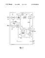
- FIG. 3shows a memory system 80 according to another embodiment of the invention that corrects drifts of the signal timing.
- the memory system 80operates under control of a memory controller 82 that controls eight memory devices 84 through commands issued over the control data bus 46 and through the master clock signal MCLK carried by the master clock bus 47 . Additionally, the memory controller 82 transmits data to and receives data from the memory devices 84 over the data bus 48 and provides the data clock signal DCLK synchronously with the data DAT to enable latching of the data DAT at the memory devices 84 .
- FIG. 4shows the structure of one of the memory devices 84 in greater detail in which the memory device 84 receives control data CDAT at the control data latches 54 .
- the latches 54latch the control data CDAT in response to the delayed master clock CCLKD produced by the delay-locked loop 58 .
- the logic control circuit 56activates the I/O interface 62 to transfer data from the memory array 64 to the output FIFO 94 .
- the data DATare held in the FIFO register 94 until the delayed output clock signal DCLKO activates the FIFO register 94 .
- the coarse and fine venires 96provide the delayed output data clock signal DCLKO in response to the delayed master clock signal CCLKD.
- the fine vernier 96is a variable delay line having its delay time controlled by the logic control circuit 56 .
- the fine vernier 96is selectively adjustable to adjust the delay between the delayed master clock signal CCLKD and the delayed output clock signal DCLKO by increments of approximately 150 ps.
- the fine vernier 96therefore activates the FIFO register 94 to transmit the read data before or after the specified leading edge of the master clock MCLK.
- the fine vernier 96thus allows each memory device 84 to be “tuned” to compensate for routing delay differences between various memory devices 84 and the memory controller 82 .
- the memory device 84 of FIG. 4also provides the delayed output data clock signal DCLKO to the data clock bus 50 as an echo clock signal ECHOCLK.
- the echo clock signal ECHOCLKtravels to the memory controller 82 on the data clock bus 50 coincident with the output data DAT traveling on the data bus 48 .
- the propagation times of signals on the data clock bus 50 and the data bus 48are substantially the same. Therefore, drifts in the timing of echo clock signal ECHOCLK timing will mirror drifts in timing of the data DAT.
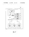
- the memory controller 82can thus continuously monitor and correct variations in routing delays, as will be described now with reference to FIG. 5 .
- the memory controller 82receives the echo clock signal ECHOCLK from the data clock bus 50 .
- the echo clock signal ECHOCLKis applied to respective first inputs of five phase comparators 102 .
- the second inputs of the phase comparators 102are driven by respective outputs of a multiple output delay-locked loop 104 driven by the master clock signal MCLK.
- the delay-locked loop 104provides phase-shifted output signals at the frequency of the master clock signal MCLK with respective positive or negative phase shifts relative to the master clock signal MCLK.
- Each of the phase comparators 102compares the echo clock signal ECHOCLK to the respective output of the delay-locked loop and outputs a respective phase compare signal ⁇ 1 - ⁇ 5 .
- a phase logic circuit 108receives the phase signals ⁇ 1 - ⁇ 5 and identifies the approximate phase shift of the echo clock signal ECHOCLK relative to the master clock signal MCLK by comparing the phase signals ⁇ 1 - ⁇ 5 .
- the phase logic circuit 108then provides phase error signals ⁇ ERROR to a logic control circuit 110 indicating the phase shift and other conditions, including the direction of the phase shift.
- the logic control circuit 110uses the phase error signals ⁇ ERROR to determine whether or not the echo clock signal ECHOCLK is within one vernier increment of the master clock signal MCLK. If the echo clock signal ECHOCLK is not within one vernier increment of the master clock signal MCLK, the logic control circuit 110 sends control data (in the next set of control data addressed to the memory device 84 ) to command the memory device 84 to adjust the vernier by one or more increments. In response to the control data from the memory controller 82 , the logic control circuit 56 ( FIG. 4 ) establishes a new fine adjust signal ADJ_F to adjust the setting of the fine vernier 96 (FIG. 4 ).
- the delay of the fine vernier 96changes the delay of the delayed output clock signal DCLKO correspondingly. Because the delayed output clock signal DCLKO controls timing of data DAT on the data bus 48 , the revised output data signal DCLKO changes the timing of data DAT as instructed by the memory controller 82 .
- the memory controller 82thus continuously monitors and corrects the timing of the memory devices 84 such that the data DAT arrive at the memory controller 82 coincident with edges of the master clock signal MCLK.
- FIG. 6is a block diagram of a computer system 200 that contains the memory controller 82 of FIG. 5 and three of the memory devices 84 of FIG. 4 .
- the computer system 200includes a processor 202 for performing computer functions such as executing software to perform desired calculations and tasks.
- the processor 202also includes command, address and data buses 210 to activate the memory controller 82 , thereby controlling reading from and writing to the memory devices 84 .
- One or more input devices 204such as a keypad or a mouse, are coupled to the processor 202 and allow an operator to manually input data thereto.
- One or more output devices 206are coupled to the processor 202 to display or otherwise output data generated by the processor 202 . Examples of output devices include a printer and a video display unit.
- One or more data storage devices 208are coupled to the processor to store data on or retrieve data from external storage media (not shown). Examples of storage devices 208 and storage media include drives that accept hard and floppy disks, tape cassettes and compact-disk read-only memories.
- the echo clock signal ECHOCLKmay be carried by a separate signal line, rather than being carried by the data clock bus 50 .
- the memory controller 82can employ other phase comparing circuits in place of the delay-locked loop 104 and bank of phase comparators 102 .
- the embodiment described hereinadjusts both the coarse and fine verniers 95 , 96 , where the drift of timing in not excessive, the memory controller 42 may transmit data adjusting only the fine vernier 96 .
- the logic control circuit 56keeps track of the total phase shift of the fine vernier 96 so that, if the fine vernier 96 reaches its adjustment limit or would move the phase shift past 360°, the logic control circuit 56 increments the coarse vernier 95 by one clock period and returns the fine vernier 95 to a lower setting referenced to the new course vernier setting. Accordingly, the invention is not limited except as by the appended claims.
Landscapes
- Dram (AREA)
Abstract
Description
Claims (24)
Priority Applications (1)
| Application Number | Priority Date | Filing Date | Title |
|---|---|---|---|
| US08/798,227US6912680B1 (en) | 1997-02-11 | 1997-02-11 | Memory system with dynamic timing correction |
Applications Claiming Priority (1)
| Application Number | Priority Date | Filing Date | Title |
|---|---|---|---|
| US08/798,227US6912680B1 (en) | 1997-02-11 | 1997-02-11 | Memory system with dynamic timing correction |
Publications (1)
| Publication Number | Publication Date |
|---|---|
| US6912680B1true US6912680B1 (en) | 2005-06-28 |
Family
ID=34679438
Family Applications (1)
| Application Number | Title | Priority Date | Filing Date |
|---|---|---|---|
| US08/798,227Expired - Fee RelatedUS6912680B1 (en) | 1997-02-11 | 1997-02-11 | Memory system with dynamic timing correction |
Country Status (1)
| Country | Link |
|---|---|
| US (1) | US6912680B1 (en) |
Cited By (25)
| Publication number | Priority date | Publication date | Assignee | Title |
|---|---|---|---|---|
| US20040170072A1 (en)* | 2001-04-24 | 2004-09-02 | Rambus Inc. | Method and apparatus for coordinating memory operations among diversely-located memory components |
| US20060181944A1 (en)* | 2005-02-17 | 2006-08-17 | Chung Hoe-Ju | Daisy chained multi-device system and operating method |
| US20060273834A1 (en)* | 2005-05-20 | 2006-12-07 | Patrick Heyne | Delay locked loop and method for setting a delay chain |
| US20070070792A1 (en)* | 2005-09-29 | 2007-03-29 | Hynix Semiconductor Inc. | Output controller with test unit |
| US20070120800A1 (en)* | 2005-11-30 | 2007-05-31 | Kentaro Teranishi | Display Control Circuit |
| US20070194818A1 (en)* | 2006-02-22 | 2007-08-23 | Hynix Semiconductor Inc. | Phase locked loop circuit having set initial locking level and control method thereof |
| US20070217559A1 (en)* | 2006-03-16 | 2007-09-20 | Rambus Inc. | Signaling system with adaptive timing calibration |
| US7301831B2 (en) | 2004-09-15 | 2007-11-27 | Rambus Inc. | Memory systems with variable delays for write data signals |
| US20070297250A1 (en)* | 2006-06-27 | 2007-12-27 | Samsung Electronics Co., Ltd. | Data processing apparatus and method using FIFO device |
| US20080002802A1 (en)* | 2006-06-29 | 2008-01-03 | Hynix Semiconductor Inc. | Phase locked loop |
| US20080068057A1 (en)* | 2006-09-14 | 2008-03-20 | Hynix Semiconductor Inc. | PLL circuit and method of controlling the same |
| US20080068058A1 (en)* | 2006-09-14 | 2008-03-20 | Hynix Semiconductor Inc. | PLL circuit having loop filter and method of driving the same |
| US20080284527A1 (en)* | 2007-05-16 | 2008-11-20 | Kwan-Dong Kim | Phase locked loop and method for operating the same |
| US20080288806A1 (en)* | 2007-05-14 | 2008-11-20 | Hynix Semiconductor Inc. | Clock generation circuit and semiconductor memory apparatus having the same |
| US20080307285A1 (en)* | 2007-06-08 | 2008-12-11 | Samsung Electronics Co., Ltd. | Memory devices and systems including error-correction coding and methods for error-correction coding |
| US20090168944A1 (en)* | 2007-12-28 | 2009-07-02 | Hynix Semiconductor, Inc. | Low pass filter and lock detector circuit |
| US20100180150A1 (en)* | 2009-01-12 | 2010-07-15 | Micron Technology, Inc. | Systems and methods for monitoring a memory system |
| US20110204951A1 (en)* | 2010-02-25 | 2011-08-25 | Hynix Semiconductor Inc. | Semiconductor apparatus |
| US8320202B2 (en) | 2001-04-24 | 2012-11-27 | Rambus Inc. | Clocked memory system with termination component |
| WO2013066774A1 (en)* | 2011-11-01 | 2013-05-10 | Rambus Inc. | Data transmission using delayed timing signals |
| US20140153582A1 (en)* | 1998-04-01 | 2014-06-05 | Mosaid Technologies Incorporated | Method and apparatus for providing a packet buffer random access memory |
| US20150295720A1 (en)* | 2014-04-11 | 2015-10-15 | Guardtime IP Holdings, Ltd. | System and Method for Sequential Data Signatures |
| US9349488B2 (en)* | 2014-05-13 | 2016-05-24 | SK Hynix Inc. | Semiconductor memory apparatus |
| US10049763B2 (en) | 2014-05-13 | 2018-08-14 | SK Hynix Inc. | Semiconductor memory apparatus |
| CN115691590A (en)* | 2021-07-26 | 2023-02-03 | 美光科技公司 | Method and related apparatus and system for improving timing in a memory device |
Citations (238)
| Publication number | Priority date | Publication date | Assignee | Title |
|---|---|---|---|---|
| US3633174A (en) | 1970-04-14 | 1972-01-04 | Us Navy | Memory system having self-adjusting strobe timing |
| US4004100A (en) | 1974-08-14 | 1977-01-18 | Nippon Electric Company, Ltd. | Group frame synchronization system |
| US4077016A (en) | 1977-02-22 | 1978-02-28 | Ncr Corporation | Apparatus and method for inhibiting false locking of a phase-locked loop |
| US4096402A (en) | 1975-12-29 | 1978-06-20 | Mostek Corporation | MOSFET buffer for TTL logic input and method of operation |
| US4404474A (en) | 1981-02-06 | 1983-09-13 | Rca Corporation | Active load pulse generating circuit |
| US4481625A (en) | 1981-10-21 | 1984-11-06 | Elxsi | High speed data bus system |
| US4508983A (en) | 1983-02-10 | 1985-04-02 | Motorola, Inc. | MOS Analog switch driven by complementary, minimally skewed clock signals |
| US4511846A (en) | 1982-05-24 | 1985-04-16 | Fairchild Camera And Instrument Corporation | Deskewing time-critical signals in automatic test equipment |
| US4514647A (en) | 1983-08-01 | 1985-04-30 | At&T Bell Laboratories | Chipset synchronization arrangement |
| US4524448A (en) | 1979-11-09 | 1985-06-18 | Nixdorf Computer Ag | Variable delay unit for data synchronizer using phase-sensitive counter to vary the delay |
| EP0171720A2 (en) | 1984-08-07 | 1986-02-19 | Kabushiki Kaisha Toshiba | Data delay/memory circuit |
| US4573017A (en) | 1984-01-03 | 1986-02-25 | Motorola, Inc. | Unitary phase and frequency adjust network for a multiple frequency digital phase locked loop |
| US4600895A (en) | 1985-04-26 | 1986-07-15 | Minnesota Mining And Manufacturing Company | Precision phase synchronization of free-running oscillator output signal to reference signal |
| US4603320A (en) | 1983-04-13 | 1986-07-29 | Anico Research, Ltd. Inc. | Connector interface |
| US4638187A (en) | 1985-10-01 | 1987-01-20 | Vtc Incorporated | CMOS output buffer providing high drive current with minimum output signal distortion |
| US4638451A (en) | 1983-05-03 | 1987-01-20 | Texas Instruments Incorporated | Microprocessor system with programmable interface |
| US4687951A (en) | 1984-10-29 | 1987-08-18 | Texas Instruments Incorporated | Fuse link for varying chip operating parameters |
| US4727541A (en) | 1984-12-06 | 1988-02-23 | Fujitsu Limited | Hierarchical data transmission system |
| US4746996A (en)* | 1984-06-26 | 1988-05-24 | Hitachi, Ltd. | Skew error correction circuit for video signal reproducing apparatus |
| US4773085A (en) | 1987-06-12 | 1988-09-20 | Bell Communications Research, Inc. | Phase and frequency detector circuits |
| US4789796A (en) | 1985-12-23 | 1988-12-06 | U.S. Philips Corporation | Output buffer having sequentially-switched output |
| EP0295515A1 (en) | 1987-06-05 | 1988-12-21 | Anritsu Corporation | Signal generating apparatus |
| US4818995A (en) | 1986-05-19 | 1989-04-04 | Hitachi Ltd. | Parallel transmission system |
| US4893087A (en) | 1988-01-07 | 1990-01-09 | Motorola, Inc. | Low voltage and low power frequency synthesizer |
| US4902986A (en) | 1989-01-30 | 1990-02-20 | Asix Systems Corporation | Phased locked loop to provide precise frequency and phase tracking of two signals |
| US4953128A (en) | 1986-12-16 | 1990-08-28 | Mitsubishi Denki Kabushiki Kaisha | Variable delay circuit for delaying input data |
| JPH02112317U (en) | 1989-02-27 | 1990-09-07 | ||
| US4958088A (en) | 1989-06-19 | 1990-09-18 | Micron Technology, Inc. | Low power three-stage CMOS input buffer with controlled switching |
| US4972470A (en) | 1987-08-06 | 1990-11-20 | Steven Farago | Programmable connector |
| US4984204A (en) | 1988-01-28 | 1991-01-08 | Hitachi, Ltd. | High speed sensor system using a level shift circuit |
| US4984255A (en) | 1989-11-15 | 1991-01-08 | National Semiconductor Corporation | Edge transition insensitive delay line system and method |
| EP0406786A1 (en) | 1989-07-04 | 1991-01-09 | ALCATEL ITALIA S.p.A. | Device for transforming a type "D" flip-flop into a flip-flop called type "B" able to sample data both on leading and trailing edges of the clock signal |
| US5020023A (en)* | 1989-02-23 | 1991-05-28 | International Business Machines Corporation | Automatic vernier synchronization of skewed data streams |
| US5038115A (en) | 1990-05-29 | 1991-08-06 | Myers Glen A | Method and apparatus for frequency independent phase tracking of input signals in receiving systems and the like |
| EP0450871A2 (en) | 1990-03-30 | 1991-10-09 | Xerox Corporation | Interfaces for transmission lines |
| US5062082A (en) | 1990-09-04 | 1991-10-29 | Samsung Electronics Co., Ltd. | Semiconductor memory device with delay in address predecoder circuit independent from ATD |
| US5075569A (en) | 1989-03-17 | 1991-12-24 | Tektronix, Inc. | Output device circuit and method to minimize impedance fluctuations during crossover |
| US5086500A (en) | 1987-08-07 | 1992-02-04 | Tektronix, Inc. | Synchronized system by adjusting independently clock signals arriving at a plurality of integrated circuits |
| US5087828A (en) | 1990-02-14 | 1992-02-11 | Daiichi Denshi Kogyo Kabushiki Kaisha | Timing circuit for single line serial data |
| JPH04135311A (en) | 1990-09-27 | 1992-05-08 | Nec Corp | Semiconductor integrated circuit |
| US5120990A (en) | 1990-06-29 | 1992-06-09 | Analog Devices, Inc. | Apparatus for generating multiple phase clock signals and phase detector therefor |
| US5122690A (en) | 1990-10-16 | 1992-06-16 | General Electric Company | Interface circuits including driver circuits with switching noise reduction |
| US5128560A (en) | 1991-03-22 | 1992-07-07 | Micron Technology, Inc. | Boosted supply output driver circuit for driving an all N-channel output stage |
| US5128563A (en) | 1990-11-28 | 1992-07-07 | Micron Technology, Inc. | CMOS bootstrapped output driver method and circuit |
| US5130565A (en)* | 1991-09-06 | 1992-07-14 | Xerox Corporation | Self calibrating PWM utilizing feedback loop for adjusting duty cycles of output signal |
| US5134311A (en) | 1990-06-07 | 1992-07-28 | International Business Machines Corporation | Self-adjusting impedance matching driver |
| EP0476585A3 (en) | 1990-09-18 | 1992-08-19 | Fujitsu Limited | Reference delay generator and electronic device using the same |
| US5150186A (en) | 1991-03-06 | 1992-09-22 | Micron Technology, Inc. | CMOS output pull-up driver |
| US5165046A (en) | 1989-11-06 | 1992-11-17 | Micron Technology, Inc. | High speed CMOS driver circuit |
| US5168199A (en)* | 1991-08-14 | 1992-12-01 | Loral Corporation | Horizontal linearity correction circuitry for cathode ray tube display |
| US5179298A (en) | 1990-01-17 | 1993-01-12 | Matsushita Electric Industrial Co., Ltd. | CMOS buffer circuit which is not influenced by bounce noise |
| US5182524A (en)* | 1992-03-10 | 1993-01-26 | The Regents Of The University Of Calif. | Method and apparatus for stabilizing pulsed microwave amplifiers |
| US5194765A (en) | 1991-06-28 | 1993-03-16 | At&T Bell Laboratories | Digitally controlled element sizing |
| US5212601A (en) | 1991-05-03 | 1993-05-18 | Western Digital Corporation | Disk drive data synchronizer with window shift synthesis |
| JPH05136664A (en) | 1991-08-14 | 1993-06-01 | Advantest Corp | Variable delay circuit |
| US5220208A (en) | 1991-04-29 | 1993-06-15 | Texas Instruments Incorporated | Circuitry and method for controlling current in an electronic circuit |
| US5223755A (en) | 1990-12-26 | 1993-06-29 | Xerox Corporation | Extended frequency range variable delay locked loop for clock synchronization |
| US5229929A (en)* | 1990-11-30 | 1993-07-20 | Honda Giken Kogyo Kabushiki Kaisha | Output peak current correction for PWM invertors |
| US5233314A (en) | 1992-03-27 | 1993-08-03 | Cyrix Corporation | Integrated charge-pump phase-locked loop circuit |
| US5233564A (en) | 1990-06-08 | 1993-08-03 | Kabushiki Kaisha Toshiba | Multiport memory with test signal generating circuit controlling data transfer from ram port to sam port |
| US5239206A (en) | 1990-03-06 | 1993-08-24 | Advanced Micro Devices, Inc. | Synchronous circuit with clock skew compensating function and circuits utilizing same |
| US5243703A (en) | 1990-04-18 | 1993-09-07 | Rambus, Inc. | Apparatus for synchronously generating clock signals in a data processing system |
| US5254883A (en) | 1992-04-22 | 1993-10-19 | Rambus, Inc. | Electrical current source circuitry for a bus |
| US5256989A (en) | 1991-05-03 | 1993-10-26 | Motorola, Inc. | Lock detection for a phase lock loop |
| US5257294A (en) | 1990-11-13 | 1993-10-26 | National Semiconductor Corporation | Phase-locked loop circuit and method |
| JPH05282868A (en) | 1992-04-02 | 1993-10-29 | Fujitsu Ltd | Semiconductor memory device |
| US5268639A (en) | 1992-06-05 | 1993-12-07 | Rambus, Inc. | Testing timing parameters of high speed integrated circuit devices |
| US5272729A (en) | 1991-09-20 | 1993-12-21 | International Business Machines Corporation | Clock signal latency elimination network |
| US5274276A (en) | 1992-06-26 | 1993-12-28 | Micron Technology, Inc. | Output driver circuit comprising a programmable circuit for determining the potential at the output node and the method of implementing the circuit |
| US5276642A (en) | 1991-07-15 | 1994-01-04 | Micron Technology, Inc. | Method for performing a split read/write operation in a dynamic random access memory |
| US5278460A (en) | 1992-04-07 | 1994-01-11 | Micron Technology, Inc. | Voltage compensating CMOS input buffer |
| US5281865A (en) | 1990-11-28 | 1994-01-25 | Hitachi, Ltd. | Flip-flop circuit |
| US5283631A (en) | 1991-11-01 | 1994-02-01 | Hewlett-Packard Co. | Programmable capacitance delay element having inverters controlled by adjustable voltage to offset temperature and voltage supply variations |
| US5289580A (en) | 1991-05-10 | 1994-02-22 | Unisys Corporation | Programmable multiple I/O interface controller |
| US5295164A (en) | 1991-12-23 | 1994-03-15 | Apple Computer, Inc. | Apparatus for providing a system clock locked to an external clock over a wide range of frequencies |
| US5304952A (en) | 1993-05-10 | 1994-04-19 | National Semiconductor Corporation | Lock sensor circuit and method for phase lock loop circuits |
| US5311481A (en) | 1992-12-17 | 1994-05-10 | Micron Technology, Inc. | Wordline driver circuit having a directly gated pull-down device |
| US5311483A (en) | 1990-11-20 | 1994-05-10 | Oki Electric Industry Co., Ltd. | Synchronous type semiconductor memory |
| US5313431A (en) | 1992-02-13 | 1994-05-17 | Mitsubishi Denki Kabushiki Kaisha | Multiport semiconductor memory device |
| US5315388A (en) | 1991-11-19 | 1994-05-24 | General Instrument Corporation | Multiple serial access memory for use in feedback systems such as motion compensated television |
| US5315269A (en) | 1991-07-31 | 1994-05-24 | Nec Corporation | Phase-locked loop |
| US5321368A (en) | 1992-02-27 | 1994-06-14 | Siemens Aktiengesellschaft | Synchronized, digital sequential circuit |
| US5337285A (en) | 1993-05-21 | 1994-08-09 | Rambus, Inc. | Method and apparatus for power control in devices |
| US5341405A (en) | 1991-06-11 | 1994-08-23 | Digital Equipment Corporation | Data recovery apparatus and methods |
| US5347177A (en) | 1993-01-14 | 1994-09-13 | Lipp Robert J | System for interconnecting VLSI circuits with transmission line characteristics |
| US5347179A (en) | 1993-04-15 | 1994-09-13 | Micron Semiconductor, Inc. | Inverting output driver circuit for reducing electron injection into the substrate |
| US5355391A (en) | 1992-03-06 | 1994-10-11 | Rambus, Inc. | High speed bus system |
| US5367649A (en) | 1988-05-20 | 1994-11-22 | Waferscale Integration, Inc. | Programmable controller |
| WO1994029871A1 (en) | 1993-06-14 | 1994-12-22 | Rambus, Inc. | Method and apparatus for writing to memory components |
| US5379299A (en) | 1992-04-16 | 1995-01-03 | The Johns Hopkins University | High speed propagation delay compensation network |
| US5390308A (en) | 1992-04-15 | 1995-02-14 | Rambus, Inc. | Method and apparatus for address mapping of dynamic random access memory |
| US5400283A (en) | 1993-12-13 | 1995-03-21 | Micron Semiconductor, Inc. | RAM row decode circuitry that utilizes a precharge circuit that is deactivated by a feedback from an activated word line driver |
| US5402389A (en) | 1994-03-08 | 1995-03-28 | Motorola, Inc. | Synchronous memory having parallel output data paths |
| US5408640A (en) | 1990-02-21 | 1995-04-18 | Digital Equipment Corporation | Phase delay compensator using gating signal generated by a synchronizer for loading and shifting of bit pattern to produce clock phases corresponding to frequency changes |
| US5410263A (en) | 1992-05-28 | 1995-04-25 | Intel Corporation | Delay line loop for on-chip clock synthesis with zero skew and 50% duty cycle |
| US5416436A (en) | 1992-09-22 | 1995-05-16 | Francen Telecom | Method for time delaying a signal and corresponding delay circuit |
| US5416909A (en) | 1990-09-14 | 1995-05-16 | Vlsi Technology, Inc. | Input/output controller circuit using a single transceiver to serve multiple input/output ports and method therefor |
| US5420544A (en) | 1992-12-28 | 1995-05-30 | Mitsubishi Denki Kabushiki Kaisha | Semiconductor integrated circuit, method of designing the same and method of manufacturing the same |
| EP0655834A1 (en) | 1993-11-25 | 1995-05-31 | Nec Corporation | Delay circuit using capacitor and transistor |
| EP0655741A2 (en) | 1993-11-29 | 1995-05-31 | Kabushiki Kaisha Toshiba | Memory device and serial-parallel data transform circuit |
| US5424687A (en) | 1993-08-23 | 1995-06-13 | Nec Corporation | PLL frequency synthesizer and PLL frequency synthesizing method capable of obtaining high-speed lock-up and highly-reliable oscillation |
| US5428311A (en) | 1993-06-30 | 1995-06-27 | Sgs-Thomson Microelectronics, Inc. | Fuse circuitry to control the propagation delay of an IC |
| US5428317A (en) | 1994-09-06 | 1995-06-27 | Motorola, Inc. | Phase locked loop with low power feedback path and method of operation |
| US5430676A (en) | 1993-06-02 | 1995-07-04 | Rambus, Inc. | Dynamic random access memory system |
| US5430408A (en) | 1993-03-08 | 1995-07-04 | Texas Instruments Incorporated | Transmission gate circuit |
| US5432823A (en) | 1992-03-06 | 1995-07-11 | Rambus, Inc. | Method and circuitry for minimizing clock-data skew in a bus system |
| US5438545A (en) | 1993-12-21 | 1995-08-01 | Goldstar Electron Co., Ltd. | Data output buffer of semiconductor memory device for preventing noises |
| US5440260A (en) | 1991-08-14 | 1995-08-08 | Advantest Corporation | Variable delay circuit |
| US5440514A (en) | 1994-03-08 | 1995-08-08 | Motorola Inc. | Write control for a memory using a delay locked loop |
| WO1995022206A1 (en) | 1994-02-15 | 1995-08-17 | Rambus, Inc. | Delay-locked loop |
| WO1995022200A1 (en) | 1994-02-15 | 1995-08-17 | Rambus, Inc. | Voltage controlled phase shifter with unlimited range |
| US5444667A (en) | 1993-04-02 | 1995-08-22 | Nec Corporation | Semiconductor synchronous memory device having input circuit for producing constant main control signal operative to allow timing generator to latch command signals |
| US5446696A (en) | 1993-05-28 | 1995-08-29 | Rambus, Inc. | Method and apparatus for implementing refresh in a synchronous DRAM system |
| US5448193A (en) | 1992-11-05 | 1995-09-05 | At&T Corp. | Normalization of apparent propagation delay |
| US5451898A (en) | 1993-11-12 | 1995-09-19 | Rambus, Inc. | Bias circuit and differential amplifier having stabilized output swing |
| US5457407A (en) | 1994-07-06 | 1995-10-10 | Sony Electronics Inc. | Binary weighted reference circuit for a variable impedance output buffer |
| EP0680049A2 (en) | 1994-04-29 | 1995-11-02 | Mosaid Technologies Incorporated | Synchronizer |
| US5465076A (en) | 1991-10-04 | 1995-11-07 | Nippondenso Co., Ltd. | Programmable delay line programmable delay circuit and digital controlled oscillator |
| US5473575A (en) | 1990-04-18 | 1995-12-05 | Rambus, Inc. | Integrated circuit I/O using a high performance bus interface |
| US5473639A (en) | 1993-07-26 | 1995-12-05 | Hewlett-Packard Company | Clock recovery apparatus with means for sensing an out of lock condition |
| US5473274A (en) | 1992-09-14 | 1995-12-05 | Nec America, Inc. | Local clock generator |
| US5485490A (en) | 1992-05-28 | 1996-01-16 | Rambus, Inc. | Method and circuitry for clock synchronization |
| US5488321A (en) | 1993-04-07 | 1996-01-30 | Rambus, Inc. | Static high speed comparator |
| US5489864A (en) | 1995-02-24 | 1996-02-06 | Intel Corporation | Delay interpolation circuitry |
| US5497355A (en) | 1994-06-03 | 1996-03-05 | Intel Corporation | Synchronous address latching for memory arrays |
| US5497127A (en) | 1994-12-14 | 1996-03-05 | David Sarnoff Research Center, Inc. | Wide frequency range CMOS relaxation oscillator with variable hysteresis |
| US5498990A (en) | 1991-11-05 | 1996-03-12 | Monolithic System Technology, Inc. | Reduced CMOS-swing clamping circuit for bus lines |
| US5500808A (en) | 1991-01-24 | 1996-03-19 | Synopsys, Inc. | Apparatus and method for estimating time delays using unmapped combinational logic networks |
| US5502672A (en) | 1994-02-03 | 1996-03-26 | Hyundai Electronics Industries Co., Ltd. | Data output buffer control circuit |
| EP0703663A1 (en) | 1994-09-21 | 1996-03-27 | STMicroelectronics S.r.l. | Programmable digital delay unit |
| EP0704975A1 (en) | 1994-09-29 | 1996-04-03 | Nec Corporation | Digital phase locked loop having coarse and fine stepsize variable delay lines |
| EP0704848A2 (en) | 1994-09-28 | 1996-04-03 | Nec Corporation | Semiconductor pipeline memory device eliminating time loss due to difference between pipeline stages from data access |
| US5506814A (en) | 1993-05-28 | 1996-04-09 | Micron Technology, Inc. | Video random access memory device and method implementing independent two WE nibble control |
| WO1996010866A1 (en) | 1994-09-30 | 1996-04-11 | Rambus, Inc. | Cmos dynamic latching input buffer circuit |
| US5508638A (en) | 1994-02-24 | 1996-04-16 | Micron Technology, Inc. | Low current redundancy fuse assembly |
| US5515403A (en) | 1994-06-21 | 1996-05-07 | Dsc Communications Corporation | Apparatus and method for clock alignment and switching |
| US5532714A (en) | 1992-07-22 | 1996-07-02 | Spx Corporation | Method and apparatus for combining video images on a pixel basis |
| US5539345A (en) | 1992-12-30 | 1996-07-23 | Digital Equipment Corporation | Phase detector apparatus |
| US5544124A (en) | 1995-03-13 | 1996-08-06 | Micron Technology, Inc. | Optimization circuitry and control for a synchronous memory device with programmable latency period |
| US5544203A (en) | 1993-02-17 | 1996-08-06 | Texas Instruments Incorporated | Fine resolution digital delay line with coarse and fine adjustment stages |
| US5550783A (en)* | 1995-04-19 | 1996-08-27 | Alliance Semiconductor Corporation | Phase shift correction circuit for monolithic random access memory |
| US5550515A (en) | 1995-01-27 | 1996-08-27 | Opti, Inc. | Multiphase clock synthesizer having a plurality of phase shifted inputs to a plurality of phase comparators in a phase locked loop |
| US5552727A (en) | 1993-10-06 | 1996-09-03 | Mitsubishi Denki Kabushiki Kaisha | Digital phase locked loop circuit |
| US5555429A (en) | 1989-03-09 | 1996-09-10 | Micron Technology, Inc. | Multiport RAM based multiprocessor |
| US5557781A (en) | 1993-07-15 | 1996-09-17 | Vlsi Technology Inc. | Combination asynchronous cache system and automatic clock tuning device and method therefor |
| US5557224A (en) | 1994-04-15 | 1996-09-17 | International Business Machines Corporation | Apparatus and method for generating a phase-controlled clock signal |
| US5563546A (en) | 1993-08-13 | 1996-10-08 | Nec Corporation | Selector circuit selecting and outputting voltage applied to one of first and second terminal in response to voltage level applied to first terminal |
| US5568075A (en) | 1994-04-08 | 1996-10-22 | International Business Machines Corporation | Timing signal generator |
| US5568077A (en) | 1994-11-07 | 1996-10-22 | Mitsubishi Denki Kabushiki Kaisha | Latch circuit |
| US5572557A (en) | 1993-06-02 | 1996-11-05 | Nec Corporation | Semiconductor integrated circuit device including PLL circuit |
| US5572722A (en) | 1992-05-28 | 1996-11-05 | Texas Instruments Incorporated | Time skewing arrangement for operating random access memory in synchronism with a data processor |
| US5576645A (en) | 1995-06-05 | 1996-11-19 | Hughes Aircraft Company | Sample and hold flip-flop for CMOS logic |
| US5577236A (en)* | 1994-12-30 | 1996-11-19 | International Business Machines Corporation | Memory controller for reading data from synchronous RAM |
| US5577079A (en) | 1994-07-28 | 1996-11-19 | Victor Company Of Japan, Ltd. | Phase comparing circuit and PLL circuit |
| US5579326A (en) | 1994-01-31 | 1996-11-26 | Sgs-Thomson Microelectronics, Inc. | Method and apparatus for programming signal timing |
| US5578940A (en) | 1995-04-04 | 1996-11-26 | Rambus, Inc. | Modular bus with single or double parallel termination |
| US5578941A (en) | 1995-08-23 | 1996-11-26 | Micron Technology, Inc. | Voltage compensating CMOS input buffer circuit |
| US5581197A (en) | 1995-05-31 | 1996-12-03 | Hewlett-Packard Co. | Method of programming a desired source resistance for a driver stage |
| US5589788A (en) | 1994-05-12 | 1996-12-31 | Hewlett-Packard Company | Timing adjustment circuit |
| US5590073A (en) | 1993-11-30 | 1996-12-31 | Sony Corporation | Random access memory having flash memory |
| US5594690A (en) | 1995-12-15 | 1997-01-14 | Unisys Corporation | Integrated circuit memory having high speed and low power by selectively coupling compensation components to a pulse generator |
| US5619473A (en) | 1994-08-23 | 1997-04-08 | Sharp Kabushiki Kaisha | Semiconductor memory device with dual address memory read amplifiers |
| EP0767538A1 (en) | 1995-10-05 | 1997-04-09 | Telefonaktiebolaget Lm Ericsson | Method and device for generating a signal |
| US5621739A (en) | 1996-05-07 | 1997-04-15 | Intel Corporation | Method and apparatus for buffer self-test and characterization |
| US5621690A (en) | 1995-04-28 | 1997-04-15 | Intel Corporation | Nonvolatile memory blocking architecture and redundancy |
| US5621340A (en) | 1995-08-02 | 1997-04-15 | Rambus Inc. | Differential comparator for amplifying small swing signals to a full swing output |
| US5627780A (en) | 1994-08-26 | 1997-05-06 | Sgs-Thomson Microelectronics Limited | Testing a non-volatile memory |
| US5627791A (en) | 1996-02-16 | 1997-05-06 | Micron Technology, Inc. | Multiple bank memory with auto refresh to specified bank |
| US5631872A (en) | 1995-08-14 | 1997-05-20 | Nec Corporation | Low power consumption semiconductor dynamic random access memory device by reusing residual electric charge on bit line pairs |
| US5636173A (en) | 1995-06-07 | 1997-06-03 | Micron Technology, Inc. | Auto-precharge during bank selection |
| US5636174A (en) | 1996-01-11 | 1997-06-03 | Cirrus Logic, Inc. | Fast cycle time-low latency dynamic random access memories and systems and methods using the same |
| US5636163A (en) | 1986-07-30 | 1997-06-03 | Mitsubishi Denki Kabushiki Kaisha | Random access memory with a plurality amplifier groups for reading and writing in normal and test modes |
| US5638335A (en) | 1995-05-22 | 1997-06-10 | Hitachi, Ltd. | Semiconductor device |
| US5646904A (en) | 1994-10-25 | 1997-07-08 | Oki Electric Industry Co., Ltd. | Semicoductor memory with a timing controlled for receiving data at a semiconductor memory module to be accessed |
| US5652530A (en) | 1995-09-29 | 1997-07-29 | Intel Corporation | Method and apparatus for reducing clock-data skew by clock shifting |
| US5657289A (en) | 1995-08-30 | 1997-08-12 | Micron Technology, Inc. | Expandable data width SAM for a multiport RAM |
| US5663921A (en) | 1994-02-18 | 1997-09-02 | Sgs-Thomson Microelectronics S.R.L. | Internal timing method and circuit for programmable memories |
| US5666313A (en) | 1991-11-29 | 1997-09-09 | Mitsubishi Denki Kabushiki Kaisha | Semiconductor memory device with complete inhibition of boosting of word line drive signal and method thereof |
| US5666322A (en) | 1995-09-21 | 1997-09-09 | Nec Electronics, Inc. | Phase-locked loop timing controller in an integrated circuit memory |
| US5668763A (en) | 1996-02-26 | 1997-09-16 | Fujitsu Limited | Semiconductor memory for increasing the number of half good memories by selecting and using good memory blocks |
| US5668774A (en) | 1995-05-22 | 1997-09-16 | Mitsubishi Denki Kabushiki Kaisha | Dynamic semiconductor memory device having fast operation mode and operating with low current consumption |
| US5673005A (en)* | 1995-08-18 | 1997-09-30 | International Business Machine Corporation | Time standard circuit with delay line oscillator |
| US5675588A (en) | 1993-09-20 | 1997-10-07 | Fujitsu Limited | Testing apparatus for transmission system |
| US5675274A (en) | 1994-12-13 | 1997-10-07 | Kabushiki Kaisha Toshiba | Semiconductor clock signal generation circuit |
| WO1997042557A2 (en) | 1996-05-07 | 1997-11-13 | Rambus, Inc. | Asynchronous request/synchronous data dynamic random access memory |
| US5692165A (en)* | 1995-09-12 | 1997-11-25 | Micron Electronics Inc. | Memory controller with low skew control signal |
| US5694065A (en) | 1994-08-16 | 1997-12-02 | Burr-Brown Corporation | Switching control circuitry for low noise CMOS inverter |
| US5708611A (en) | 1994-11-22 | 1998-01-13 | Mitsubishi Denki Kabushiki Kaisha | Synchronous semiconductor memory device |
| US5712580A (en) | 1996-02-14 | 1998-01-27 | International Business Machines Corporation | Linear phase detector for half-speed quadrature clocking architecture |
| US5719508A (en) | 1996-02-01 | 1998-02-17 | Northern Telecom, Ltd. | Loss of lock detector for master timing generator |
| WO1997014289A3 (en) | 1995-10-19 | 1998-04-02 | Rambus Inc | Protocol for communication with dynamic memory |
| US5737342A (en) | 1996-05-31 | 1998-04-07 | Quantum Corporation | Method for in-chip testing of digital circuits of a synchronously sampled data detection channel |
| US5740123A (en) | 1996-08-29 | 1998-04-14 | Fujitsu Limited | Semiconductor integrated circuit for changing pulse width according to frequency of external signal |
| US5751665A (en) | 1995-07-14 | 1998-05-12 | Oki Electric Industry Co., Ltd. | Clock distributing circuit |
| US5767715A (en) | 1995-09-29 | 1998-06-16 | Siemens Medical Systems, Inc. | Method and apparatus for generating timing pulses accurately skewed relative to clock |
| US5768177A (en) | 1996-05-13 | 1998-06-16 | Nec Corporation | Controlled delay circuit for use in synchronized semiconductor memory |
| US5774699A (en) | 1995-07-04 | 1998-06-30 | Kabushiki Kaisha Toshiba | System controller for controlling switching operations of various operation clocks for CPU, DRAM, and the like |
| US5778214A (en) | 1994-12-09 | 1998-07-07 | Oki Electric Industry Co., Ltd. | Bit-phase aligning circuit |
| US5781499A (en) | 1995-11-10 | 1998-07-14 | Nec Corporation | Semiconductor memory device |
| US5784422A (en) | 1996-08-05 | 1998-07-21 | Transcrypt International, Inc. | Apparatus and method for accurate synchronization with inbound data packets at relatively low sampling rates |
| US5790612A (en) | 1996-02-29 | 1998-08-04 | Silicon Graphics, Inc. | System and method to reduce jitter in digital delay-locked loops |
| US5789947A (en) | 1995-09-21 | 1998-08-04 | Nippon Precision Circuits Inc. | Phase comparator |
| US5794020A (en) | 1995-06-16 | 1998-08-11 | Hitachi, Ltd. | Data transfer apparatus fetching reception data at maximum margin of timing |
| US5805931A (en) | 1996-02-09 | 1998-09-08 | Micron Technology, Inc. | Programmable bandwidth I/O port and a communication interface using the same port having a plurality of serial access memories capable of being configured for a variety of protocols |
| US5812619A (en) | 1996-02-28 | 1998-09-22 | Advanced Micro Devices, Inc. | Digital phase lock loop and system for digital clock recovery |
| US5822314A (en) | 1995-05-31 | 1998-10-13 | Motorola, Inc. | Communications system and method of operation |
| US5831929A (en) | 1997-04-04 | 1998-11-03 | Micron Technology, Inc. | Memory device with staggered data paths |
| US5841707A (en) | 1995-11-29 | 1998-11-24 | Texas Instruments Incorporated | Apparatus and method for a programmable interval timing generator in a semiconductor memory |
| US5852378A (en) | 1997-02-11 | 1998-12-22 | Micron Technology, Inc. | Low-skew differential signal converter |
| US5872959A (en) | 1996-09-10 | 1999-02-16 | Lsi Logic Corporation | Method and apparatus for parallel high speed data transfer |
| US5889829A (en) | 1997-01-07 | 1999-03-30 | Microchip Technology Incorporated | Phase locked loop with improved lock time and stability |
| US5898242A (en) | 1990-04-04 | 1999-04-27 | Unisys Corporation | Self-calibrating clock circuit employing a continuously variable delay module in a feedback loop |
| US5898674A (en) | 1995-11-14 | 1999-04-27 | Paradyne Corporation | System and method for performing non-disruptive diagnostics through a frame relay circuit |
| US5917760A (en) | 1996-09-20 | 1999-06-29 | Sldram, Inc. | De-skewing data signals in a memory system |
| US5920518A (en) | 1997-02-11 | 1999-07-06 | Micron Technology, Inc. | Synchronous clock generator including delay-locked loop |
| US5926047A (en) | 1997-08-29 | 1999-07-20 | Micron Technology, Inc. | Synchronous clock generator including a delay-locked loop signal loss detector |
| US5926436A (en) | 1990-10-15 | 1999-07-20 | Kabushiki Kaisha Toshiba | Semiconductor memory device |
| US5940609A (en) | 1997-08-29 | 1999-08-17 | Micorn Technology, Inc. | Synchronous clock generator including a false lock detector |
| US5940608A (en) | 1997-02-11 | 1999-08-17 | Micron Technology, Inc. | Method and apparatus for generating an internal clock signal that is synchronized to an external clock signal |
| US5946244A (en) | 1997-03-05 | 1999-08-31 | Micron Technology, Inc. | Delay-locked loop with binary-coupled capacitor |
| US5953386A (en) | 1996-06-20 | 1999-09-14 | Lsi Logic Corporation | High speed clock recovery circuit using complimentary dividers |
| US5953284A (en) | 1997-07-09 | 1999-09-14 | Micron Technology, Inc. | Method and apparatus for adaptively adjusting the timing of a clock signal used to latch digital signals, and memory device using same |
| US5964884A (en) | 1996-09-30 | 1999-10-12 | Advanced Micro Devices, Inc. | Self-timed pulse control circuit |
| US5990719A (en) | 1997-10-07 | 1999-11-23 | Intel Corporation | Adaptive filtering scheme for sampling phase relations of clock networks |
| US6005823A (en) | 1997-06-20 | 1999-12-21 | Micron Technology, Inc. | Memory device with pipelined column address path |
| US6011732A (en) | 1997-08-20 | 2000-01-04 | Micron Technology, Inc. | Synchronous clock generator including a compound delay-locked loop |
| US6016282A (en) | 1998-05-28 | 2000-01-18 | Micron Technology, Inc. | Clock vernier adjustment |
| US6023489A (en) | 1995-05-24 | 2000-02-08 | Leica Geosystems Inc. | Method and apparatus for code synchronization in a global positioning system receiver |
| US6029250A (en) | 1998-09-09 | 2000-02-22 | Micron Technology, Inc. | Method and apparatus for adaptively adjusting the timing offset between a clock signal and digital signals transmitted coincident with that clock signal, and memory device and system using same |
| US6038219A (en) | 1996-12-31 | 2000-03-14 | Paradyne Corporation | User-configurable frame relay network |
| US6101197A (en) | 1997-09-18 | 2000-08-08 | Micron Technology, Inc. | Method and apparatus for adjusting the timing of signals over fine and coarse ranges |
| US6105157A (en) | 1998-01-30 | 2000-08-15 | Credence Systems Corporation | Salphasic timing calibration system for an integrated circuit tester |
| US6147916A (en) | 1998-11-04 | 2000-11-14 | Fujitsu Limited | Semiconductor memory device with precharge voltage correction circuit |
| US6147905A (en) | 1998-07-30 | 2000-11-14 | Fujitsu Limited | Non-volatile semiconductor memory device |
| US6160423A (en) | 1998-03-16 | 2000-12-12 | Jazio, Inc. | High speed source synchronous signaling for interfacing VLSI CMOS circuits to transmission lines |
| US6269451B1 (en) | 1998-02-27 | 2001-07-31 | Micron Technology, Inc. | Method and apparatus for adjusting data timing by delaying clock signal |
| US6298450B1 (en) | 1997-12-31 | 2001-10-02 | Intel Corporation | Detecting states of signals |
| US6338127B1 (en) | 1998-08-28 | 2002-01-08 | Micron Technology, Inc. | Method and apparatus for resynchronizing a plurality of clock signals used to latch respective digital signals, and memory device using same |
- 1997
- 1997-02-11USUS08/798,227patent/US6912680B1/ennot_activeExpired - Fee Related
Patent Citations (252)
| Publication number | Priority date | Publication date | Assignee | Title |
|---|---|---|---|---|
| US3633174A (en) | 1970-04-14 | 1972-01-04 | Us Navy | Memory system having self-adjusting strobe timing |
| US4004100A (en) | 1974-08-14 | 1977-01-18 | Nippon Electric Company, Ltd. | Group frame synchronization system |
| US4096402A (en) | 1975-12-29 | 1978-06-20 | Mostek Corporation | MOSFET buffer for TTL logic input and method of operation |
| US4077016A (en) | 1977-02-22 | 1978-02-28 | Ncr Corporation | Apparatus and method for inhibiting false locking of a phase-locked loop |
| US4524448A (en) | 1979-11-09 | 1985-06-18 | Nixdorf Computer Ag | Variable delay unit for data synchronizer using phase-sensitive counter to vary the delay |
| US4404474A (en) | 1981-02-06 | 1983-09-13 | Rca Corporation | Active load pulse generating circuit |
| US4481625A (en) | 1981-10-21 | 1984-11-06 | Elxsi | High speed data bus system |
| US4511846A (en) | 1982-05-24 | 1985-04-16 | Fairchild Camera And Instrument Corporation | Deskewing time-critical signals in automatic test equipment |
| US4508983A (en) | 1983-02-10 | 1985-04-02 | Motorola, Inc. | MOS Analog switch driven by complementary, minimally skewed clock signals |
| US4603320A (en) | 1983-04-13 | 1986-07-29 | Anico Research, Ltd. Inc. | Connector interface |
| US4638451A (en) | 1983-05-03 | 1987-01-20 | Texas Instruments Incorporated | Microprocessor system with programmable interface |
| US4514647A (en) | 1983-08-01 | 1985-04-30 | At&T Bell Laboratories | Chipset synchronization arrangement |
| US4573017A (en) | 1984-01-03 | 1986-02-25 | Motorola, Inc. | Unitary phase and frequency adjust network for a multiple frequency digital phase locked loop |
| US4746996A (en)* | 1984-06-26 | 1988-05-24 | Hitachi, Ltd. | Skew error correction circuit for video signal reproducing apparatus |
| EP0171720A2 (en) | 1984-08-07 | 1986-02-19 | Kabushiki Kaisha Toshiba | Data delay/memory circuit |
| US4687951A (en) | 1984-10-29 | 1987-08-18 | Texas Instruments Incorporated | Fuse link for varying chip operating parameters |
| US4727541A (en) | 1984-12-06 | 1988-02-23 | Fujitsu Limited | Hierarchical data transmission system |
| US4600895A (en) | 1985-04-26 | 1986-07-15 | Minnesota Mining And Manufacturing Company | Precision phase synchronization of free-running oscillator output signal to reference signal |
| US4638187B1 (en) | 1985-10-01 | 1993-03-02 | Cypress Semiconductor Minnesot | |
| US4638187A (en) | 1985-10-01 | 1987-01-20 | Vtc Incorporated | CMOS output buffer providing high drive current with minimum output signal distortion |
| US4789796A (en) | 1985-12-23 | 1988-12-06 | U.S. Philips Corporation | Output buffer having sequentially-switched output |
| US4818995A (en) | 1986-05-19 | 1989-04-04 | Hitachi Ltd. | Parallel transmission system |
| US5636163A (en) | 1986-07-30 | 1997-06-03 | Mitsubishi Denki Kabushiki Kaisha | Random access memory with a plurality amplifier groups for reading and writing in normal and test modes |
| US4953128A (en) | 1986-12-16 | 1990-08-28 | Mitsubishi Denki Kabushiki Kaisha | Variable delay circuit for delaying input data |
| EP0295515A1 (en) | 1987-06-05 | 1988-12-21 | Anritsu Corporation | Signal generating apparatus |
| US4773085A (en) | 1987-06-12 | 1988-09-20 | Bell Communications Research, Inc. | Phase and frequency detector circuits |
| US4972470A (en) | 1987-08-06 | 1990-11-20 | Steven Farago | Programmable connector |
| US5086500A (en) | 1987-08-07 | 1992-02-04 | Tektronix, Inc. | Synchronized system by adjusting independently clock signals arriving at a plurality of integrated circuits |
| US4893087A (en) | 1988-01-07 | 1990-01-09 | Motorola, Inc. | Low voltage and low power frequency synthesizer |
| US4984204A (en) | 1988-01-28 | 1991-01-08 | Hitachi, Ltd. | High speed sensor system using a level shift circuit |
| US5367649A (en) | 1988-05-20 | 1994-11-22 | Waferscale Integration, Inc. | Programmable controller |
| US4902986B1 (en) | 1989-01-30 | 1998-09-01 | Credence Systems Corp | Phased locked loop to provide precise frequency and phase tracking of two signals |
| US4902986A (en) | 1989-01-30 | 1990-02-20 | Asix Systems Corporation | Phased locked loop to provide precise frequency and phase tracking of two signals |
| US5020023A (en)* | 1989-02-23 | 1991-05-28 | International Business Machines Corporation | Automatic vernier synchronization of skewed data streams |
| JPH02112317U (en) | 1989-02-27 | 1990-09-07 | ||
| US5555429A (en) | 1989-03-09 | 1996-09-10 | Micron Technology, Inc. | Multiport RAM based multiprocessor |
| US5075569A (en) | 1989-03-17 | 1991-12-24 | Tektronix, Inc. | Output device circuit and method to minimize impedance fluctuations during crossover |
| US4958088A (en) | 1989-06-19 | 1990-09-18 | Micron Technology, Inc. | Low power three-stage CMOS input buffer with controlled switching |
| EP0406786A1 (en) | 1989-07-04 | 1991-01-09 | ALCATEL ITALIA S.p.A. | Device for transforming a type "D" flip-flop into a flip-flop called type "B" able to sample data both on leading and trailing edges of the clock signal |
| US5165046A (en) | 1989-11-06 | 1992-11-17 | Micron Technology, Inc. | High speed CMOS driver circuit |
| US4984255A (en) | 1989-11-15 | 1991-01-08 | National Semiconductor Corporation | Edge transition insensitive delay line system and method |
| US5179298A (en) | 1990-01-17 | 1993-01-12 | Matsushita Electric Industrial Co., Ltd. | CMOS buffer circuit which is not influenced by bounce noise |
| US5087828A (en) | 1990-02-14 | 1992-02-11 | Daiichi Denshi Kogyo Kabushiki Kaisha | Timing circuit for single line serial data |
| US5408640A (en) | 1990-02-21 | 1995-04-18 | Digital Equipment Corporation | Phase delay compensator using gating signal generated by a synchronizer for loading and shifting of bit pattern to produce clock phases corresponding to frequency changes |
| US5239206A (en) | 1990-03-06 | 1993-08-24 | Advanced Micro Devices, Inc. | Synchronous circuit with clock skew compensating function and circuits utilizing same |
| EP0450871A2 (en) | 1990-03-30 | 1991-10-09 | Xerox Corporation | Interfaces for transmission lines |
| US5898242A (en) | 1990-04-04 | 1999-04-27 | Unisys Corporation | Self-calibrating clock circuit employing a continuously variable delay module in a feedback loop |
| US5657481A (en) | 1990-04-18 | 1997-08-12 | Rambus, Inc. | Memory device with a phase locked loop circuitry |
| US6067592A (en) | 1990-04-18 | 2000-05-23 | Rambus Inc. | System having a synchronous memory device |
| US5243703A (en) | 1990-04-18 | 1993-09-07 | Rambus, Inc. | Apparatus for synchronously generating clock signals in a data processing system |
| US5473575A (en) | 1990-04-18 | 1995-12-05 | Rambus, Inc. | Integrated circuit I/O using a high performance bus interface |
| US6101152A (en) | 1990-04-18 | 2000-08-08 | Rambus Inc. | Method of operating a synchronous memory device |
| US5513327A (en) | 1990-04-18 | 1996-04-30 | Rambus, Inc. | Integrated circuit I/O using a high performance bus interface |
| US5038115A (en) | 1990-05-29 | 1991-08-06 | Myers Glen A | Method and apparatus for frequency independent phase tracking of input signals in receiving systems and the like |
| US5134311A (en) | 1990-06-07 | 1992-07-28 | International Business Machines Corporation | Self-adjusting impedance matching driver |
| US5233564A (en) | 1990-06-08 | 1993-08-03 | Kabushiki Kaisha Toshiba | Multiport memory with test signal generating circuit controlling data transfer from ram port to sam port |
| US5120990A (en) | 1990-06-29 | 1992-06-09 | Analog Devices, Inc. | Apparatus for generating multiple phase clock signals and phase detector therefor |
| US5062082A (en) | 1990-09-04 | 1991-10-29 | Samsung Electronics Co., Ltd. | Semiconductor memory device with delay in address predecoder circuit independent from ATD |
| US5416909A (en) | 1990-09-14 | 1995-05-16 | Vlsi Technology, Inc. | Input/output controller circuit using a single transceiver to serve multiple input/output ports and method therefor |
| EP0476585A3 (en) | 1990-09-18 | 1992-08-19 | Fujitsu Limited | Reference delay generator and electronic device using the same |
| JPH04135311A (en) | 1990-09-27 | 1992-05-08 | Nec Corp | Semiconductor integrated circuit |
| US5926436A (en) | 1990-10-15 | 1999-07-20 | Kabushiki Kaisha Toshiba | Semiconductor memory device |
| US5122690A (en) | 1990-10-16 | 1992-06-16 | General Electric Company | Interface circuits including driver circuits with switching noise reduction |
| US5257294A (en) | 1990-11-13 | 1993-10-26 | National Semiconductor Corporation | Phase-locked loop circuit and method |
| US5311483A (en) | 1990-11-20 | 1994-05-10 | Oki Electric Industry Co., Ltd. | Synchronous type semiconductor memory |
| US5128563A (en) | 1990-11-28 | 1992-07-07 | Micron Technology, Inc. | CMOS bootstrapped output driver method and circuit |
| US5281865A (en) | 1990-11-28 | 1994-01-25 | Hitachi, Ltd. | Flip-flop circuit |
| US5229929A (en)* | 1990-11-30 | 1993-07-20 | Honda Giken Kogyo Kabushiki Kaisha | Output peak current correction for PWM invertors |
| US5223755A (en) | 1990-12-26 | 1993-06-29 | Xerox Corporation | Extended frequency range variable delay locked loop for clock synchronization |
| US5500808A (en) | 1991-01-24 | 1996-03-19 | Synopsys, Inc. | Apparatus and method for estimating time delays using unmapped combinational logic networks |
| US5150186A (en) | 1991-03-06 | 1992-09-22 | Micron Technology, Inc. | CMOS output pull-up driver |
| US5128560A (en) | 1991-03-22 | 1992-07-07 | Micron Technology, Inc. | Boosted supply output driver circuit for driving an all N-channel output stage |
| US5220208A (en) | 1991-04-29 | 1993-06-15 | Texas Instruments Incorporated | Circuitry and method for controlling current in an electronic circuit |
| US5212601A (en) | 1991-05-03 | 1993-05-18 | Western Digital Corporation | Disk drive data synchronizer with window shift synthesis |
| US5256989A (en) | 1991-05-03 | 1993-10-26 | Motorola, Inc. | Lock detection for a phase lock loop |
| US5289580A (en) | 1991-05-10 | 1994-02-22 | Unisys Corporation | Programmable multiple I/O interface controller |
| US5341405A (en) | 1991-06-11 | 1994-08-23 | Digital Equipment Corporation | Data recovery apparatus and methods |
| US5194765A (en) | 1991-06-28 | 1993-03-16 | At&T Bell Laboratories | Digitally controlled element sizing |
| US5276642A (en) | 1991-07-15 | 1994-01-04 | Micron Technology, Inc. | Method for performing a split read/write operation in a dynamic random access memory |
| US5315269A (en) | 1991-07-31 | 1994-05-24 | Nec Corporation | Phase-locked loop |
| JPH05136664A (en) | 1991-08-14 | 1993-06-01 | Advantest Corp | Variable delay circuit |
| US5440260A (en) | 1991-08-14 | 1995-08-08 | Advantest Corporation | Variable delay circuit |
| US5168199A (en)* | 1991-08-14 | 1992-12-01 | Loral Corporation | Horizontal linearity correction circuitry for cathode ray tube display |
| US5130565A (en)* | 1991-09-06 | 1992-07-14 | Xerox Corporation | Self calibrating PWM utilizing feedback loop for adjusting duty cycles of output signal |
| US5272729A (en) | 1991-09-20 | 1993-12-21 | International Business Machines Corporation | Clock signal latency elimination network |
| US5465076A (en) | 1991-10-04 | 1995-11-07 | Nippondenso Co., Ltd. | Programmable delay line programmable delay circuit and digital controlled oscillator |
| US5283631A (en) | 1991-11-01 | 1994-02-01 | Hewlett-Packard Co. | Programmable capacitance delay element having inverters controlled by adjustable voltage to offset temperature and voltage supply variations |
| US5498990A (en) | 1991-11-05 | 1996-03-12 | Monolithic System Technology, Inc. | Reduced CMOS-swing clamping circuit for bus lines |
| US5315388A (en) | 1991-11-19 | 1994-05-24 | General Instrument Corporation | Multiple serial access memory for use in feedback systems such as motion compensated television |
| US5666313A (en) | 1991-11-29 | 1997-09-09 | Mitsubishi Denki Kabushiki Kaisha | Semiconductor memory device with complete inhibition of boosting of word line drive signal and method thereof |
| US5295164A (en) | 1991-12-23 | 1994-03-15 | Apple Computer, Inc. | Apparatus for providing a system clock locked to an external clock over a wide range of frequencies |
| US5313431A (en) | 1992-02-13 | 1994-05-17 | Mitsubishi Denki Kabushiki Kaisha | Multiport semiconductor memory device |
| US5321368A (en) | 1992-02-27 | 1994-06-14 | Siemens Aktiengesellschaft | Synchronized, digital sequential circuit |
| US5355391A (en) | 1992-03-06 | 1994-10-11 | Rambus, Inc. | High speed bus system |
| US5432823A (en) | 1992-03-06 | 1995-07-11 | Rambus, Inc. | Method and circuitry for minimizing clock-data skew in a bus system |
| US5182524A (en)* | 1992-03-10 | 1993-01-26 | The Regents Of The University Of Calif. | Method and apparatus for stabilizing pulsed microwave amplifiers |
| US5233314A (en) | 1992-03-27 | 1993-08-03 | Cyrix Corporation | Integrated charge-pump phase-locked loop circuit |
| JPH05282868A (en) | 1992-04-02 | 1993-10-29 | Fujitsu Ltd | Semiconductor memory device |
| US5278460A (en) | 1992-04-07 | 1994-01-11 | Micron Technology, Inc. | Voltage compensating CMOS input buffer |
| US5361002A (en) | 1992-04-07 | 1994-11-01 | Micron Technology, Inc. | Voltage compensating CMOS input buffer |
| US5390308A (en) | 1992-04-15 | 1995-02-14 | Rambus, Inc. | Method and apparatus for address mapping of dynamic random access memory |
| US5379299A (en) | 1992-04-16 | 1995-01-03 | The Johns Hopkins University | High speed propagation delay compensation network |
| US5254883A (en) | 1992-04-22 | 1993-10-19 | Rambus, Inc. | Electrical current source circuitry for a bus |
| US5410263A (en) | 1992-05-28 | 1995-04-25 | Intel Corporation | Delay line loop for on-chip clock synthesis with zero skew and 50% duty cycle |
| US5485490A (en) | 1992-05-28 | 1996-01-16 | Rambus, Inc. | Method and circuitry for clock synchronization |
| US5572722A (en) | 1992-05-28 | 1996-11-05 | Texas Instruments Incorporated | Time skewing arrangement for operating random access memory in synchronism with a data processor |
| US5268639A (en) | 1992-06-05 | 1993-12-07 | Rambus, Inc. | Testing timing parameters of high speed integrated circuit devices |
| US5274276A (en) | 1992-06-26 | 1993-12-28 | Micron Technology, Inc. | Output driver circuit comprising a programmable circuit for determining the potential at the output node and the method of implementing the circuit |
| US5532714A (en) | 1992-07-22 | 1996-07-02 | Spx Corporation | Method and apparatus for combining video images on a pixel basis |
| US5473274A (en) | 1992-09-14 | 1995-12-05 | Nec America, Inc. | Local clock generator |
| US5416436A (en) | 1992-09-22 | 1995-05-16 | Francen Telecom | Method for time delaying a signal and corresponding delay circuit |
| US5448193A (en) | 1992-11-05 | 1995-09-05 | At&T Corp. | Normalization of apparent propagation delay |
| US5311481A (en) | 1992-12-17 | 1994-05-10 | Micron Technology, Inc. | Wordline driver circuit having a directly gated pull-down device |
| US5420544A (en) | 1992-12-28 | 1995-05-30 | Mitsubishi Denki Kabushiki Kaisha | Semiconductor integrated circuit, method of designing the same and method of manufacturing the same |
| US5539345A (en) | 1992-12-30 | 1996-07-23 | Digital Equipment Corporation | Phase detector apparatus |
| US5347177A (en) | 1993-01-14 | 1994-09-13 | Lipp Robert J | System for interconnecting VLSI circuits with transmission line characteristics |
| US5544203A (en) | 1993-02-17 | 1996-08-06 | Texas Instruments Incorporated | Fine resolution digital delay line with coarse and fine adjustment stages |
| US5430408A (en) | 1993-03-08 | 1995-07-04 | Texas Instruments Incorporated | Transmission gate circuit |
| US5444667A (en) | 1993-04-02 | 1995-08-22 | Nec Corporation | Semiconductor synchronous memory device having input circuit for producing constant main control signal operative to allow timing generator to latch command signals |
| US5488321A (en) | 1993-04-07 | 1996-01-30 | Rambus, Inc. | Static high speed comparator |
| US5347179A (en) | 1993-04-15 | 1994-09-13 | Micron Semiconductor, Inc. | Inverting output driver circuit for reducing electron injection into the substrate |
| US5304952A (en) | 1993-05-10 | 1994-04-19 | National Semiconductor Corporation | Lock sensor circuit and method for phase lock loop circuits |
| US5337285A (en) | 1993-05-21 | 1994-08-09 | Rambus, Inc. | Method and apparatus for power control in devices |
| US5446696A (en) | 1993-05-28 | 1995-08-29 | Rambus, Inc. | Method and apparatus for implementing refresh in a synchronous DRAM system |
| US5506814A (en) | 1993-05-28 | 1996-04-09 | Micron Technology, Inc. | Video random access memory device and method implementing independent two WE nibble control |
| US5572557A (en) | 1993-06-02 | 1996-11-05 | Nec Corporation | Semiconductor integrated circuit device including PLL circuit |
| US5430676A (en) | 1993-06-02 | 1995-07-04 | Rambus, Inc. | Dynamic random access memory system |
| WO1994029871A1 (en) | 1993-06-14 | 1994-12-22 | Rambus, Inc. | Method and apparatus for writing to memory components |
| US5428311A (en) | 1993-06-30 | 1995-06-27 | Sgs-Thomson Microelectronics, Inc. | Fuse circuitry to control the propagation delay of an IC |
| US5557781A (en) | 1993-07-15 | 1996-09-17 | Vlsi Technology Inc. | Combination asynchronous cache system and automatic clock tuning device and method therefor |
| US5473639A (en) | 1993-07-26 | 1995-12-05 | Hewlett-Packard Company | Clock recovery apparatus with means for sensing an out of lock condition |
| US5563546A (en) | 1993-08-13 | 1996-10-08 | Nec Corporation | Selector circuit selecting and outputting voltage applied to one of first and second terminal in response to voltage level applied to first terminal |
| US5424687A (en) | 1993-08-23 | 1995-06-13 | Nec Corporation | PLL frequency synthesizer and PLL frequency synthesizing method capable of obtaining high-speed lock-up and highly-reliable oscillation |
| US5675588A (en) | 1993-09-20 | 1997-10-07 | Fujitsu Limited | Testing apparatus for transmission system |
| US5552727A (en) | 1993-10-06 | 1996-09-03 | Mitsubishi Denki Kabushiki Kaisha | Digital phase locked loop circuit |
| US5451898A (en) | 1993-11-12 | 1995-09-19 | Rambus, Inc. | Bias circuit and differential amplifier having stabilized output swing |
| EP0655834A1 (en) | 1993-11-25 | 1995-05-31 | Nec Corporation | Delay circuit using capacitor and transistor |
| EP0655741A2 (en) | 1993-11-29 | 1995-05-31 | Kabushiki Kaisha Toshiba | Memory device and serial-parallel data transform circuit |
| US5590073A (en) | 1993-11-30 | 1996-12-31 | Sony Corporation | Random access memory having flash memory |
| US5574698A (en) | 1993-12-13 | 1996-11-12 | Micron Technology, Inc. | Ram row decode circuitry that utilizes a precharge circuit that is deactivated by a feedback from an activated word line driver |
| US5400283A (en) | 1993-12-13 | 1995-03-21 | Micron Semiconductor, Inc. | RAM row decode circuitry that utilizes a precharge circuit that is deactivated by a feedback from an activated word line driver |
| US5438545A (en) | 1993-12-21 | 1995-08-01 | Goldstar Electron Co., Ltd. | Data output buffer of semiconductor memory device for preventing noises |
| US5579326A (en) | 1994-01-31 | 1996-11-26 | Sgs-Thomson Microelectronics, Inc. | Method and apparatus for programming signal timing |
| US5502672A (en) | 1994-02-03 | 1996-03-26 | Hyundai Electronics Industries Co., Ltd. | Data output buffer control circuit |
| WO1995022200A1 (en) | 1994-02-15 | 1995-08-17 | Rambus, Inc. | Voltage controlled phase shifter with unlimited range |
| WO1995022206A1 (en) | 1994-02-15 | 1995-08-17 | Rambus, Inc. | Delay-locked loop |
| US5614855A (en) | 1994-02-15 | 1997-03-25 | Rambus, Inc. | Delay-locked loop |
| US5663921A (en) | 1994-02-18 | 1997-09-02 | Sgs-Thomson Microelectronics S.R.L. | Internal timing method and circuit for programmable memories |
| US5508638A (en) | 1994-02-24 | 1996-04-16 | Micron Technology, Inc. | Low current redundancy fuse assembly |
| US5440514A (en) | 1994-03-08 | 1995-08-08 | Motorola Inc. | Write control for a memory using a delay locked loop |
| US5402389A (en) | 1994-03-08 | 1995-03-28 | Motorola, Inc. | Synchronous memory having parallel output data paths |
| US5568075A (en) | 1994-04-08 | 1996-10-22 | International Business Machines Corporation | Timing signal generator |
| US5557224A (en) | 1994-04-15 | 1996-09-17 | International Business Machines Corporation | Apparatus and method for generating a phase-controlled clock signal |
| EP0680049A2 (en) | 1994-04-29 | 1995-11-02 | Mosaid Technologies Incorporated | Synchronizer |
| US5589788A (en) | 1994-05-12 | 1996-12-31 | Hewlett-Packard Company | Timing adjustment circuit |
| US5497355A (en) | 1994-06-03 | 1996-03-05 | Intel Corporation | Synchronous address latching for memory arrays |
| US5515403A (en) | 1994-06-21 | 1996-05-07 | Dsc Communications Corporation | Apparatus and method for clock alignment and switching |
| US5457407A (en) | 1994-07-06 | 1995-10-10 | Sony Electronics Inc. | Binary weighted reference circuit for a variable impedance output buffer |
| US5577079A (en) | 1994-07-28 | 1996-11-19 | Victor Company Of Japan, Ltd. | Phase comparing circuit and PLL circuit |
| US5694065A (en) | 1994-08-16 | 1997-12-02 | Burr-Brown Corporation | Switching control circuitry for low noise CMOS inverter |
| US5619473A (en) | 1994-08-23 | 1997-04-08 | Sharp Kabushiki Kaisha | Semiconductor memory device with dual address memory read amplifiers |
| US5627780A (en) | 1994-08-26 | 1997-05-06 | Sgs-Thomson Microelectronics Limited | Testing a non-volatile memory |
| US5428317A (en) | 1994-09-06 | 1995-06-27 | Motorola, Inc. | Phase locked loop with low power feedback path and method of operation |
| EP0703663A1 (en) | 1994-09-21 | 1996-03-27 | STMicroelectronics S.r.l. | Programmable digital delay unit |
| EP0704848A2 (en) | 1994-09-28 | 1996-04-03 | Nec Corporation | Semiconductor pipeline memory device eliminating time loss due to difference between pipeline stages from data access |
| EP0704975A1 (en) | 1994-09-29 | 1996-04-03 | Nec Corporation | Digital phase locked loop having coarse and fine stepsize variable delay lines |
| WO1996010866A1 (en) | 1994-09-30 | 1996-04-11 | Rambus, Inc. | Cmos dynamic latching input buffer circuit |
| US5646904A (en) | 1994-10-25 | 1997-07-08 | Oki Electric Industry Co., Ltd. | Semicoductor memory with a timing controlled for receiving data at a semiconductor memory module to be accessed |
| US5568077A (en) | 1994-11-07 | 1996-10-22 | Mitsubishi Denki Kabushiki Kaisha | Latch circuit |
| US5708611A (en) | 1994-11-22 | 1998-01-13 | Mitsubishi Denki Kabushiki Kaisha | Synchronous semiconductor memory device |
| US5778214A (en) | 1994-12-09 | 1998-07-07 | Oki Electric Industry Co., Ltd. | Bit-phase aligning circuit |
| US5675274A (en) | 1994-12-13 | 1997-10-07 | Kabushiki Kaisha Toshiba | Semiconductor clock signal generation circuit |
| US5497127A (en) | 1994-12-14 | 1996-03-05 | David Sarnoff Research Center, Inc. | Wide frequency range CMOS relaxation oscillator with variable hysteresis |
| US5577236A (en)* | 1994-12-30 | 1996-11-19 | International Business Machines Corporation | Memory controller for reading data from synchronous RAM |
| US5550515A (en) | 1995-01-27 | 1996-08-27 | Opti, Inc. | Multiphase clock synthesizer having a plurality of phase shifted inputs to a plurality of phase comparators in a phase locked loop |
| US5489864A (en) | 1995-02-24 | 1996-02-06 | Intel Corporation | Delay interpolation circuitry |
| US5544124A (en) | 1995-03-13 | 1996-08-06 | Micron Technology, Inc. | Optimization circuitry and control for a synchronous memory device with programmable latency period |
| US5578940A (en) | 1995-04-04 | 1996-11-26 | Rambus, Inc. | Modular bus with single or double parallel termination |
| US5550783A (en)* | 1995-04-19 | 1996-08-27 | Alliance Semiconductor Corporation | Phase shift correction circuit for monolithic random access memory |
| US5621690A (en) | 1995-04-28 | 1997-04-15 | Intel Corporation | Nonvolatile memory blocking architecture and redundancy |
| US5638335A (en) | 1995-05-22 | 1997-06-10 | Hitachi, Ltd. | Semiconductor device |
| US5668774A (en) | 1995-05-22 | 1997-09-16 | Mitsubishi Denki Kabushiki Kaisha | Dynamic semiconductor memory device having fast operation mode and operating with low current consumption |
| US6023489A (en) | 1995-05-24 | 2000-02-08 | Leica Geosystems Inc. | Method and apparatus for code synchronization in a global positioning system receiver |
| US5822314A (en) | 1995-05-31 | 1998-10-13 | Motorola, Inc. | Communications system and method of operation |
| US5581197A (en) | 1995-05-31 | 1996-12-03 | Hewlett-Packard Co. | Method of programming a desired source resistance for a driver stage |
| US5576645A (en) | 1995-06-05 | 1996-11-19 | Hughes Aircraft Company | Sample and hold flip-flop for CMOS logic |
| US5636173A (en) | 1995-06-07 | 1997-06-03 | Micron Technology, Inc. | Auto-precharge during bank selection |
| US5794020A (en) | 1995-06-16 | 1998-08-11 | Hitachi, Ltd. | Data transfer apparatus fetching reception data at maximum margin of timing |
| US5774699A (en) | 1995-07-04 | 1998-06-30 | Kabushiki Kaisha Toshiba | System controller for controlling switching operations of various operation clocks for CPU, DRAM, and the like |
| US5751665A (en) | 1995-07-14 | 1998-05-12 | Oki Electric Industry Co., Ltd. | Clock distributing circuit |
| US5621340A (en) | 1995-08-02 | 1997-04-15 | Rambus Inc. | Differential comparator for amplifying small swing signals to a full swing output |
| US5631872A (en) | 1995-08-14 | 1997-05-20 | Nec Corporation | Low power consumption semiconductor dynamic random access memory device by reusing residual electric charge on bit line pairs |
| US5673005A (en)* | 1995-08-18 | 1997-09-30 | International Business Machine Corporation | Time standard circuit with delay line oscillator |
| US5578941A (en) | 1995-08-23 | 1996-11-26 | Micron Technology, Inc. | Voltage compensating CMOS input buffer circuit |
| US5657289A (en) | 1995-08-30 | 1997-08-12 | Micron Technology, Inc. | Expandable data width SAM for a multiport RAM |
| US5692165A (en)* | 1995-09-12 | 1997-11-25 | Micron Electronics Inc. | Memory controller with low skew control signal |
| US5666322A (en) | 1995-09-21 | 1997-09-09 | Nec Electronics, Inc. | Phase-locked loop timing controller in an integrated circuit memory |
| US5789947A (en) | 1995-09-21 | 1998-08-04 | Nippon Precision Circuits Inc. | Phase comparator |
| US5767715A (en) | 1995-09-29 | 1998-06-16 | Siemens Medical Systems, Inc. | Method and apparatus for generating timing pulses accurately skewed relative to clock |
| US5652530A (en) | 1995-09-29 | 1997-07-29 | Intel Corporation | Method and apparatus for reducing clock-data skew by clock shifting |
| EP0767538A1 (en) | 1995-10-05 | 1997-04-09 | Telefonaktiebolaget Lm Ericsson | Method and device for generating a signal |
| WO1997014289A3 (en) | 1995-10-19 | 1998-04-02 | Rambus Inc | Protocol for communication with dynamic memory |
| US5781499A (en) | 1995-11-10 | 1998-07-14 | Nec Corporation | Semiconductor memory device |
| US5898674A (en) | 1995-11-14 | 1999-04-27 | Paradyne Corporation | System and method for performing non-disruptive diagnostics through a frame relay circuit |
| US5841707A (en) | 1995-11-29 | 1998-11-24 | Texas Instruments Incorporated | Apparatus and method for a programmable interval timing generator in a semiconductor memory |
| US5594690A (en) | 1995-12-15 | 1997-01-14 | Unisys Corporation | Integrated circuit memory having high speed and low power by selectively coupling compensation components to a pulse generator |
| US5636174A (en) | 1996-01-11 | 1997-06-03 | Cirrus Logic, Inc. | Fast cycle time-low latency dynamic random access memories and systems and methods using the same |
| US5719508A (en) | 1996-02-01 | 1998-02-17 | Northern Telecom, Ltd. | Loss of lock detector for master timing generator |
| US5805931A (en) | 1996-02-09 | 1998-09-08 | Micron Technology, Inc. | Programmable bandwidth I/O port and a communication interface using the same port having a plurality of serial access memories capable of being configured for a variety of protocols |
| US5712580A (en) | 1996-02-14 | 1998-01-27 | International Business Machines Corporation | Linear phase detector for half-speed quadrature clocking architecture |
| US5627791A (en) | 1996-02-16 | 1997-05-06 | Micron Technology, Inc. | Multiple bank memory with auto refresh to specified bank |
| US5668763A (en) | 1996-02-26 | 1997-09-16 | Fujitsu Limited | Semiconductor memory for increasing the number of half good memories by selecting and using good memory blocks |
| US5812619A (en) | 1996-02-28 | 1998-09-22 | Advanced Micro Devices, Inc. | Digital phase lock loop and system for digital clock recovery |
| US5790612A (en) | 1996-02-29 | 1998-08-04 | Silicon Graphics, Inc. | System and method to reduce jitter in digital delay-locked loops |
| WO1997042557A2 (en) | 1996-05-07 | 1997-11-13 | Rambus, Inc. | Asynchronous request/synchronous data dynamic random access memory |
| US5621739A (en) | 1996-05-07 | 1997-04-15 | Intel Corporation | Method and apparatus for buffer self-test and characterization |
| US5768177A (en) | 1996-05-13 | 1998-06-16 | Nec Corporation | Controlled delay circuit for use in synchronized semiconductor memory |
| US5737342A (en) | 1996-05-31 | 1998-04-07 | Quantum Corporation | Method for in-chip testing of digital circuits of a synchronously sampled data detection channel |
| US5953386A (en) | 1996-06-20 | 1999-09-14 | Lsi Logic Corporation | High speed clock recovery circuit using complimentary dividers |
| US5784422A (en) | 1996-08-05 | 1998-07-21 | Transcrypt International, Inc. | Apparatus and method for accurate synchronization with inbound data packets at relatively low sampling rates |
| US5740123A (en) | 1996-08-29 | 1998-04-14 | Fujitsu Limited | Semiconductor integrated circuit for changing pulse width according to frequency of external signal |
| US5872959A (en) | 1996-09-10 | 1999-02-16 | Lsi Logic Corporation | Method and apparatus for parallel high speed data transfer |
| US5917760A (en) | 1996-09-20 | 1999-06-29 | Sldram, Inc. | De-skewing data signals in a memory system |
| US5964884A (en) | 1996-09-30 | 1999-10-12 | Advanced Micro Devices, Inc. | Self-timed pulse control circuit |
| US6038219A (en) | 1996-12-31 | 2000-03-14 | Paradyne Corporation | User-configurable frame relay network |
| US5889829A (en) | 1997-01-07 | 1999-03-30 | Microchip Technology Incorporated | Phase locked loop with improved lock time and stability |
| US5940608A (en) | 1997-02-11 | 1999-08-17 | Micron Technology, Inc. | Method and apparatus for generating an internal clock signal that is synchronized to an external clock signal |
| US5920518A (en) | 1997-02-11 | 1999-07-06 | Micron Technology, Inc. | Synchronous clock generator including delay-locked loop |
| US5852378A (en) | 1997-02-11 | 1998-12-22 | Micron Technology, Inc. | Low-skew differential signal converter |
| US5946244A (en) | 1997-03-05 | 1999-08-31 | Micron Technology, Inc. | Delay-locked loop with binary-coupled capacitor |
| US6262921B1 (en) | 1997-03-05 | 2001-07-17 | Micron Technology, Inc. | Delay-locked loop with binary-coupled capacitor |
| US5831929A (en) | 1997-04-04 | 1998-11-03 | Micron Technology, Inc. | Memory device with staggered data paths |
| US6005823A (en) | 1997-06-20 | 1999-12-21 | Micron Technology, Inc. | Memory device with pipelined column address path |
| US5953284A (en) | 1997-07-09 | 1999-09-14 | Micron Technology, Inc. | Method and apparatus for adaptively adjusting the timing of a clock signal used to latch digital signals, and memory device using same |
| US6026050A (en) | 1997-07-09 | 2000-02-15 | Micron Technology, Inc. | Method and apparatus for adaptively adjusting the timing of a clock signal used to latch digital signals, and memory device using same |
| US6011732A (en) | 1997-08-20 | 2000-01-04 | Micron Technology, Inc. | Synchronous clock generator including a compound delay-locked loop |
| US5926047A (en) | 1997-08-29 | 1999-07-20 | Micron Technology, Inc. | Synchronous clock generator including a delay-locked loop signal loss detector |
| US5940609A (en) | 1997-08-29 | 1999-08-17 | Micorn Technology, Inc. | Synchronous clock generator including a false lock detector |
| US6101197A (en) | 1997-09-18 | 2000-08-08 | Micron Technology, Inc. | Method and apparatus for adjusting the timing of signals over fine and coarse ranges |
| US5990719A (en) | 1997-10-07 | 1999-11-23 | Intel Corporation | Adaptive filtering scheme for sampling phase relations of clock networks |
| US6298450B1 (en) | 1997-12-31 | 2001-10-02 | Intel Corporation | Detecting states of signals |
| US6105157A (en) | 1998-01-30 | 2000-08-15 | Credence Systems Corporation | Salphasic timing calibration system for an integrated circuit tester |
| US6269451B1 (en) | 1998-02-27 | 2001-07-31 | Micron Technology, Inc. | Method and apparatus for adjusting data timing by delaying clock signal |
| US6327196B1 (en) | 1998-02-27 | 2001-12-04 | Micron Technology, Inc. | Synchronous memory device having an adjustable data clocking circuit |
| US6378079B1 (en) | 1998-02-27 | 2002-04-23 | Micron Technology, Inc. | Computer system having memory device with adjustable data clocking |
| US6499111B2 (en) | 1998-02-27 | 2002-12-24 | Micron Technology, Inc. | Apparatus for adjusting delay of a clock signal relative to a data signal |
| US6160423A (en) | 1998-03-16 | 2000-12-12 | Jazio, Inc. | High speed source synchronous signaling for interfacing VLSI CMOS circuits to transmission lines |
| US6016282A (en) | 1998-05-28 | 2000-01-18 | Micron Technology, Inc. | Clock vernier adjustment |
| US6147905A (en) | 1998-07-30 | 2000-11-14 | Fujitsu Limited | Non-volatile semiconductor memory device |
| US6338127B1 (en) | 1998-08-28 | 2002-01-08 | Micron Technology, Inc. | Method and apparatus for resynchronizing a plurality of clock signals used to latch respective digital signals, and memory device using same |
| US6029250A (en) | 1998-09-09 | 2000-02-22 | Micron Technology, Inc. | Method and apparatus for adaptively adjusting the timing offset between a clock signal and digital signals transmitted coincident with that clock signal, and memory device and system using same |
| US6147916A (en) | 1998-11-04 | 2000-11-14 | Fujitsu Limited | Semiconductor memory device with precharge voltage correction circuit |
Non-Patent Citations (50)
| Title |
|---|
| "Draft Standard for a High-Speed Memory Interface (SyncLink)," Microprocessor and Microcomputer Standards Subcommittee of the IEEE Computer Society, Copyright 1996 by the Institute of Electrical Engineers, Inc., New York, NY, pp. 1-56. |
| Alvarez, J. et al. "A Wide-Bandwidth Low Voltage PLL for PowerPC(TM) Microprocessors" IEEE IEICE Trans. Electron., vol. E-78. No. 6, Jun. 1995, pp. 631-639. |
| Alvarez, J. et al. "A Wide-Bandwidth Low Voltage PLL for PowerPC™ Microprocessors" IEEE IEICE Trans. Electron., vol. E-78. No. 6, Jun. 1995, pp. 631-639. |
| Anonymous, "Programmable Pulse Generator", IBM Technical Disclosure Bulletin, vol. 17, No. 12, May 1975, pp. 3553-3554. |
| Anonymous, "Pulse Combining Network", IBM Technical Disclosure Bulletin, vol. 32, No. 12, May 1990, pp. 149-151. |
| Anonymous, "Variable Delay Digital Circuit", IBM Technical Disclosure Bulletin, vol. 35, No. 4A, Sep. 1992, pp. 365-366. |
| Arai, Y. et al., "A CMOS Four Channel x1K Time Memory LSI with 1-ns/b Resolution", IEEE Journal of Solid-State Circuits, vol. 27, No. 3,M, 8107 Mar., 1992, No. 3, New York, US. |
| Arai, Y. et al., "A Time Digitizer CMOS Gate-Array with a 250 ps Time Resolution", XP 000597207, IEEE Journal of Solid-State Circuits, vol. 31, No. 2, Feb. 1996. |
| Arai, Y. et al., "A CMOS Four Channel ×1K Time Memory LSI with 1-ns/b Resolution", IEEE Journal of Solid-State Circuits, vol. 27, No. 3,M, 8107 Mar., 1992, No. 3, New York, US. |
| Aviram, A. et al., "Obtaining High Speed Printing on Thermal Sensitive Special Paper With A Resistive Ribbon Print Head", IBM Technical Disclosure Bulletin, vol. 27, No. 5, Oct. 1984, pp. 3059-3060. |
| Bazes, M., "Two Novel Fully Complementary Self-Biased CMOS Differential Amplifiers", IEEE Journal of Solid-State Circuits, vol. 26, No. 2, Feb. 1991, pp. 165-168. |
| Chapman, J. et al., "A Low-Cost High-Performance CMOS Timing Vernier for ATE", IEEE International Test Conference, Ppaer 21.2, 1995, pp. 459-468. |
| Cho, J. "Digitally-Controlled PLL with Pulse Width Detection Mechanism for Error Correction", ISSCC 1997, Paper No. SA 20.3, pp. 334-335. |
| Christiansen, J., "An Integrated High Resolution CMOS Timing Generator Based on an Array of Delay Locked Loops", IEEE Journal of Solid-State Circuits, vol. 31, No. 7, Jul. 1996, pp. 952-957. |
| Combes, M. et al., "A Portable Clock Multiplier Generator Using Digital CMOS Standard Cells", IEEE Journal of Solid-State Circuits, vol. 31, No. 7, Jul. 1996, pp. 958-965. |
| Descriptive literature entitled, "400 MHz SLDRAM, 4Mx16 SLDRAM Pipelined, Eight Bank, 2.5 V Operation," pp. 1-22. |
| Descriptive literature entitled, "400 MHz SLDRAM, 4M×16 SLDRAM Pipelined, Eight Bank, 2.5 V Operation," pp. 1-22. |
| Donnelly, K. et al., "A 660 MB/s Interface Megacell Portable Circuit in 0.3 mum-0.7 mum CMOS ASIC", IEEE Journal of Solid-State Circuits, vol. 31, No. 12, Dec. 1996, pp. 1995-2001. |
| Donnelly, K. et al., "A 660 MB/s Interface Megacell Portable Circuit in 0.3 μm-0.7 μm CMOS ASIC", IEEE Journal of Solid-State Circuits, vol. 31, No. 12, Dec. 1996, pp. 1995-2001. |
| Goto, J. et al., "A PLL-Based Programmable Clock Generator with 50- to 350-MHz Oscillating Range for Video Signal Processors", IEICE Trans. Electron., vol. E77-C, No. 12, Dec. 1994, pp. 1951-1956. |
| Gustavsion, David B., et al., "IEEE Standard for Scalable Coherent Interface (SCI)," IEEE Computer Society, IEEE Std. 1596-1992, Aug. 2, 1993. |
| Hamamoto, T., 400-MHz Random Column Operating SDRAM Techniques with Self-Skew Compensation, IEEE Journal of Solid-State Circuits, vol. 33, No. 5, May 1998, pp. 770-778. |
| Ishibashi, A. et al., "High-Speed Clock Distribution Architecture Employing PLL for 0.6mum CMOS SOG", IEEE Custom Integrated Circuits Conference, 1992, pp. 27.6.1-27.6.4. |
| Ishibashi, A. et al., "High-Speed Clock Distribution Architecture Employing PLL for 0.6μm CMOS SOG", IEEE Custom Integrated Circuits Conference, 1992, pp. 27.6.1-27.6.4. |
| Kikuchi, S. et al., "A Gate-Array Based 666MHz VLSI Test System", IEEE International Test Conference, Paper 21.1, 1995, pp. 451-458. |
| Kim, B. et al., "A 30MHz High-Speed Analog/Digital PLL in 2mum CMOS", ISSCC, Feb. 1990. |
| Kim, B. et al., "A 30MHz High-Speed Analog/Digital PLL in 2μm CMOS", ISSCC, Feb. 1990. |
| Ko, U. et al., "A 30-ps Jitter, 3.6-mus Locking, 3.3-Volt Digital PLL for CMOS Gate Arrays", IEEE Custom Integrated Circuits Conference. 1993, pp. 23.3.1-23.3.4. |
| Ko, U. et al., "A 30-ps Jitter, 3.6-μs Locking, 3.3-Volt Digital PLL for CMOS Gate Arrays", IEEE Custom Integrated Circuits Conference. 1993, pp. 23.3.1-23.3.4. |
| Lee, T. et al., "A 2.5V Delay-Locked Loop for an 18Mb 500MB/s DRAM", IEEE International Solid-State Circuits Conference Digest of Technical Papers, Paper No. FA 18.6, 1994, pp. 300-301. |
| Lesmeister, G., "A Densely Integrated High Performance CMOS Tester", International Test Conference, Paper 16.2, 1991, pp. 426-429. |
| Ljuslin, C. et al., "An Integrated 16-channel CMOS Time to Digital Converter", IEEE Nuclear Science Symposium & Medical Imaging Conference Record, vol. 1, 1993, pp. 625-629. |
| Maneatis, John G., "Low-Jitter Process Independent DLL and PLL Based on Self-Biased Techniques," IEEE Journal of Solid-State Circuits, vol. 31, No. 11: pp. 1723-1732, Nov. 1996. |
| Nakamura, M. et al., "A 156 Mbps CMOS Clock Recovery Circuit for Burst-mode Transmission", Symposium on VLSI Circuits Digest of Technical Papers, 1996, pp. 122-123. |
| Nielson, E., "Inverting latches make simple VCO", EDN, Jun. 19, 1997. |
| Novof, I. et al., "Fully Integrated CMOS Phase-Locked Loop with 15 to 240 MHz Locking Range and ±50 ps Jitter", IEEE Journal of Solid-State Circuits, vol. 30, No. 11, Nov. 1995, pp. 1259-1266. |
| Park, D. et al., "Fast Acquisition Frequency Synthesizer with the Multiple Phase Detectors", IEEE Pacific Rim Conference on Communications, Computers and Signal Processing, vol. 2, May 1991, pp. 665-668. |
| Saeki, T. et al., "A 2.5-ns Clock Access, 250-MHz, 256-Mb SDRAM with Synchronous Mirror Delay", IEEE Journal of Solid-State Circuits, vol. 31, No. 11, Nov. 1996, pp. 1656-1665. |
| Santos, D. et al., "A CMOS Delay Locked Loop And Sub-Nanosecond Time-to-Digital Converter Chip", IEEE Nuclear Science Symposium and Medical Imaging Conference Record, vol. 1, Oct. 1995, pp. 289-291. |
| Shirotori, T. et al., "PLL-based, Impedance Controlled Output Buffer", 1991 Symposium on VLSI Circuits Digest of Technical Papers, pp. 49-50. |
| Sidiropoulos, S. et al., "A 700-Mb/s/pin CMOS Signaling Interface Using Current Integrating Receivers", IEEE Journal of Solid-State Circuits, vol. 32, No. 5, May 1997, pp. 681-690. |
| Sidiropoulos, S. et al., "A CMOS 500 Mbps/pin synchronous point to point link interface", IEEE Symposium on VLSI Circuits Digest of Technical Papers, 1994, pp. 43-44. |
| Sidiropoulos, S. et al., "A Semi-Digital DLL with Unlimited Phase Shift Capability and 0.08-400MHz Operating Range," in 1997 International Solid State Circuits Conference, Feb. 8, 1997, pp. 332-333. |
| Soyuer, M. et al., "A Fully Monolithic 1.25GHz CMOS Frequency Synthesizer", IEEE Symposium on VLSI Circuits Digest of Technical Papers, 1994, pp. 127-128. |
| Taguchi, M. et al., "A 40-ns 64-Mb DRAM with 64-b Parallel Data Bus Architecture", IEEE Journal of Solid-State Circuits, vol. 26, Nov. 1991, pp. 1493-1497. |
| Tanoi, S. et al., "A 250-622 MHz Deskew and Jitter-Suppressed Clock Buffer Using a Frequency- and Delay-Locked Two-Loop Architecture", 1995 Symposium on VLSI Circuits Digest of Technical Papers, vol. 11, No. 2, pp. 85-86. |
| Tanoi, S. et. al., "A 250-622 MHz Deskew and Jitter-Suppressed Clock Buffer Using Two-Loop Architecture", IEEE IEICE Trans. Electron., vol. E-79-C. No. 7, Jul. 1996, pp. 898-904. |
| von Kaenel, V. et al., "A 320 Mhz, 1.5 mW @ 1.35 V CMOS PLL for Microprocessor Clock Generation", IEEE Journal of Solid-State Circuits, vol. 31, No. 11, Nov. 1996, pp .1715-1722. |
| Watson, R. et al., "Clock Buffer Chip with Absolute Delay Regulation Over Process and Environmental Variations", IEEE Custom Integrated Circuits Conference, 1992, pp. 25.2.1-25.2.5. |
| Yoshimura, T. et al. "A 622-Mb/s Bit/Frame Synchronizer for High-Speed Backplane Data Communication", IEEE Journal of Solid-State Circuits, vol. 31, No. 7, Jul. 1996, pp. 1063-1066. |
Cited By (96)
| Publication number | Priority date | Publication date | Assignee | Title |
|---|---|---|---|---|
| US20140153582A1 (en)* | 1998-04-01 | 2014-06-05 | Mosaid Technologies Incorporated | Method and apparatus for providing a packet buffer random access memory |
| US7225292B2 (en) | 2001-04-24 | 2007-05-29 | Rambus Inc. | Memory module with termination component |
| US20050169097A1 (en)* | 2001-04-24 | 2005-08-04 | Rambus Inc. | Method and apparatus for coordinating memory operations among diversely-located memory components |
| US20060039174A1 (en)* | 2001-04-24 | 2006-02-23 | Ware Frederick A | Memory module with termination component |
| US20060069895A1 (en)* | 2001-04-24 | 2006-03-30 | Ware Frederick A | Method, system and memory controller utilizing adjustable write data delay settings |
| US20060129776A1 (en)* | 2001-04-24 | 2006-06-15 | Ware Frederick A | Method, system and memory controller utilizing adjustable read data delay settings |
| US10706910B2 (en) | 2001-04-24 | 2020-07-07 | Rambus Inc. | Memory controller |
| US10236051B2 (en) | 2001-04-24 | 2019-03-19 | Rambus Inc. | Memory controller |
| US7177998B2 (en)* | 2001-04-24 | 2007-02-13 | Rambus Inc. | Method, system and memory controller utilizing adjustable read data delay settings |
| US9741424B2 (en) | 2001-04-24 | 2017-08-22 | Rambus Inc. | Memory controller |
| US7200055B2 (en) | 2001-04-24 | 2007-04-03 | Rambus Inc. | Memory module with termination component |
| US7209397B2 (en) | 2001-04-24 | 2007-04-24 | Rambus Inc. | Memory device with clock multiplier circuit |
| US7210016B2 (en) | 2001-04-24 | 2007-04-24 | Rambus Inc. | Method, system and memory controller utilizing adjustable write data delay settings |
| US7225311B2 (en) | 2001-04-24 | 2007-05-29 | Rambus Inc. | Method and apparatus for coordinating memory operations among diversely-located memory components |
| US8214616B2 (en) | 2001-04-24 | 2012-07-03 | Rambus Inc. | Memory controller device having timing offset capability |
| US20060007761A1 (en)* | 2001-04-24 | 2006-01-12 | Ware Frederick A | Memory module with termination component |
| US20040170072A1 (en)* | 2001-04-24 | 2004-09-02 | Rambus Inc. | Method and apparatus for coordinating memory operations among diversely-located memory components |
| US9472262B2 (en) | 2001-04-24 | 2016-10-18 | Rambus Inc. | Memory controller |
| US9053778B2 (en) | 2001-04-24 | 2015-06-09 | Rambus Inc. | Memory controller that enforces strobe-to-strobe timing offset |
| US8760944B2 (en) | 2001-04-24 | 2014-06-24 | Rambus Inc. | Memory component that samples command/address signals in response to both edges of a clock signal |
| US9311976B2 (en) | 2001-04-24 | 2016-04-12 | Rambus Inc. | Memory module |
| US8717837B2 (en) | 2001-04-24 | 2014-05-06 | Rambus Inc. | Memory module |
| US8625371B2 (en) | 2001-04-24 | 2014-01-07 | Rambus Inc. | Memory component with terminated and unterminated signaling inputs |
| US8537601B2 (en) | 2001-04-24 | 2013-09-17 | Rambus Inc. | Memory controller with selective data transmission delay |
| US8462566B2 (en) | 2001-04-24 | 2013-06-11 | Rambus Inc. | Memory module with termination component |
| US8395951B2 (en) | 2001-04-24 | 2013-03-12 | Rambus Inc. | Memory controller |
| US8391039B2 (en) | 2001-04-24 | 2013-03-05 | Rambus Inc. | Memory module with termination component |
| US8359445B2 (en) | 2001-04-24 | 2013-01-22 | Rambus Inc. | Method and apparatus for signaling between devices of a memory system |
| US8320202B2 (en) | 2001-04-24 | 2012-11-27 | Rambus Inc. | Clocked memory system with termination component |
| US7484064B2 (en) | 2001-04-24 | 2009-01-27 | Rambus Inc. | Method and apparatus for signaling between devices of a memory system |
| US9229470B2 (en)* | 2004-09-15 | 2016-01-05 | Rambus Inc. | Memory controller with clock-to-strobe skew compensation |
| US8363493B2 (en) | 2004-09-15 | 2013-01-29 | Rambus Inc. | Memory controller having a write-timing calibration mode |
| US11664067B2 (en) | 2004-09-15 | 2023-05-30 | Rambus Inc. | Memory system component that enables clock-to-strobe skew compensation |
| US8493802B1 (en) | 2004-09-15 | 2013-07-23 | Rambus Inc. | Memory controller having a write-timing calibration mode |
| US7724590B2 (en) | 2004-09-15 | 2010-05-25 | Rambus Inc. | Memory controller with multiple delayed timing signals |
| US11100976B2 (en) | 2004-09-15 | 2021-08-24 | Rambus Inc. | Memory controller with clock-to-strobe skew compensation |
| US10755764B2 (en) | 2004-09-15 | 2020-08-25 | Rambus Inc. | Memory component that enables calibrated command- and data-timing signal arrival |
| US7301831B2 (en) | 2004-09-15 | 2007-11-27 | Rambus Inc. | Memory systems with variable delays for write data signals |
| US10325645B2 (en) | 2004-09-15 | 2019-06-18 | Rambus Inc. | Memory controller with clock-to-strobe skew compensation |
| US8743636B2 (en) | 2004-09-15 | 2014-06-03 | Rambus Inc. | Memory module having a write-timing calibration mode |
| US7480193B2 (en) | 2004-09-15 | 2009-01-20 | Rambus Inc. | Memory component with multiple delayed timing signals |
| US9830971B2 (en) | 2004-09-15 | 2017-11-28 | Rambus Inc. | Memory controller with clock-to-strobe skew compensation |
| US20140244923A1 (en)* | 2004-09-15 | 2014-08-28 | Rambus Inc. | Memory controller with clock-to-strobe skew compensation |
| US8218382B2 (en) | 2004-09-15 | 2012-07-10 | Rambus Inc. | Memory component having a write-timing calibration mode |
| US8045407B2 (en) | 2004-09-15 | 2011-10-25 | Rambus Inc. | Memory-write timing calibration including generation of multiple delayed timing signals |
| US9437279B2 (en) | 2004-09-15 | 2016-09-06 | Rambus Inc. | Memory controller with clock-to-strobe skew compensation |
| US20060181944A1 (en)* | 2005-02-17 | 2006-08-17 | Chung Hoe-Ju | Daisy chained multi-device system and operating method |
| US7380152B2 (en)* | 2005-02-17 | 2008-05-27 | Samsung Electronics Co., Ltd. | Daisy chained multi-device system and operating method |
| US20060273834A1 (en)* | 2005-05-20 | 2006-12-07 | Patrick Heyne | Delay locked loop and method for setting a delay chain |
| US7391245B2 (en)* | 2005-05-20 | 2008-06-24 | Infineon Technologies Ag | Delay locked loop and method for setting a delay chain |
| US7549092B2 (en) | 2005-09-29 | 2009-06-16 | Hynix Semiconductor, Inc. | Output controller with test unit |
| US20070070792A1 (en)* | 2005-09-29 | 2007-03-29 | Hynix Semiconductor Inc. | Output controller with test unit |
| US20070120800A1 (en)* | 2005-11-30 | 2007-05-31 | Kentaro Teranishi | Display Control Circuit |
| US7911458B2 (en)* | 2005-11-30 | 2011-03-22 | Toshiba Matsushita Display Technology Co., Ltd. | Display control circuit |
| US20070194818A1 (en)* | 2006-02-22 | 2007-08-23 | Hynix Semiconductor Inc. | Phase locked loop circuit having set initial locking level and control method thereof |
| US7646223B2 (en) | 2006-02-22 | 2010-01-12 | Hynix Semiconductor Inc. | Phase locked loop circuit having set initial locking level and control method thereof |
| US8121237B2 (en)* | 2006-03-16 | 2012-02-21 | Rambus Inc. | Signaling system with adaptive timing calibration |
| US11405174B2 (en) | 2006-03-16 | 2022-08-02 | Rambus Inc. | Signaling system with adaptive timing calibration |
| US11115179B2 (en) | 2006-03-16 | 2021-09-07 | Rambus Inc. | Signaling system with adaptive timing calibration |
| US10771231B2 (en) | 2006-03-16 | 2020-09-08 | Rambus Inc. | Signaling system with adaptive timing calibration |
| US10447465B2 (en) | 2006-03-16 | 2019-10-15 | Rambus Inc. | Signaling system with adaptive timing calibration |
| US9432179B2 (en) | 2006-03-16 | 2016-08-30 | Rambus Inc. | Signaling system with adaptive timing calibration |
| US20070217559A1 (en)* | 2006-03-16 | 2007-09-20 | Rambus Inc. | Signaling system with adaptive timing calibration |
| US20070297250A1 (en)* | 2006-06-27 | 2007-12-27 | Samsung Electronics Co., Ltd. | Data processing apparatus and method using FIFO device |
| US7802123B2 (en)* | 2006-06-27 | 2010-09-21 | Samsung Electronics Co., Ltd. | Data processing apparatus and method using FIFO device |
| US20080002802A1 (en)* | 2006-06-29 | 2008-01-03 | Hynix Semiconductor Inc. | Phase locked loop |
| US7864910B2 (en) | 2006-06-29 | 2011-01-04 | Hynix Semiconductor Inc. | Phase locked loop |
| US20080068057A1 (en)* | 2006-09-14 | 2008-03-20 | Hynix Semiconductor Inc. | PLL circuit and method of controlling the same |
| US7741888B2 (en) | 2006-09-14 | 2010-06-22 | Hynix Semiconductor Inc. | PLL circuit having loop filter and method of driving the same |
| US20080068058A1 (en)* | 2006-09-14 | 2008-03-20 | Hynix Semiconductor Inc. | PLL circuit having loop filter and method of driving the same |
| US7642824B2 (en) | 2006-09-14 | 2010-01-05 | Hynix Semiconductor Inc. | PLL circuit and method of controlling the same |
| US20080288806A1 (en)* | 2007-05-14 | 2008-11-20 | Hynix Semiconductor Inc. | Clock generation circuit and semiconductor memory apparatus having the same |
| US7953998B2 (en) | 2007-05-14 | 2011-05-31 | Hynix Semiconductor Inc. | Clock generation circuit and semiconductor memory apparatus having the same |
| US20080284527A1 (en)* | 2007-05-16 | 2008-11-20 | Kwan-Dong Kim | Phase locked loop and method for operating the same |
| US8063708B2 (en) | 2007-05-16 | 2011-11-22 | Hynix Semiconductor Inc. | Phase locked loop and method for operating the same |
| US8627174B2 (en)* | 2007-06-08 | 2014-01-07 | Samsung Electronics Co., Ltd. | Memory devices and systems including error-correction coding and methods for error-correction coding |
| US20080307285A1 (en)* | 2007-06-08 | 2008-12-11 | Samsung Electronics Co., Ltd. | Memory devices and systems including error-correction coding and methods for error-correction coding |
| US20090168944A1 (en)* | 2007-12-28 | 2009-07-02 | Hynix Semiconductor, Inc. | Low pass filter and lock detector circuit |
| US7876148B2 (en) | 2007-12-28 | 2011-01-25 | Hynix Semiconductor Inc. | Low pass filter and lock detector circuit |
| US8601332B2 (en) | 2009-01-12 | 2013-12-03 | Micron Technology, Inc. | Systems and methods for monitoring a memory system |
| US8234528B2 (en)* | 2009-01-12 | 2012-07-31 | Micron Technology, Inc. | Systems and methods for monitoring a memory system |
| US20120023376A1 (en)* | 2009-01-12 | 2012-01-26 | Jeddeloh Joe M | Systems and methods for monitoring a memory system |
| US8032804B2 (en)* | 2009-01-12 | 2011-10-04 | Micron Technology, Inc. | Systems and methods for monitoring a memory system |
| US20100180150A1 (en)* | 2009-01-12 | 2010-07-15 | Micron Technology, Inc. | Systems and methods for monitoring a memory system |
| US20110204951A1 (en)* | 2010-02-25 | 2011-08-25 | Hynix Semiconductor Inc. | Semiconductor apparatus |
| US8390364B2 (en) | 2010-02-25 | 2013-03-05 | Hynix Semiconductor Inc. | Internal voltage generation circuit for semiconductor apparatus |
| US9843315B2 (en) | 2011-11-01 | 2017-12-12 | Rambus Inc. | Data transmission using delayed timing signals |
| US10700671B2 (en) | 2011-11-01 | 2020-06-30 | Rambus Inc. | Data transmission using delayed timing signals |
| WO2013066774A1 (en)* | 2011-11-01 | 2013-05-10 | Rambus Inc. | Data transmission using delayed timing signals |
| US11451218B2 (en) | 2011-11-01 | 2022-09-20 | Rambus Inc. | Data transmission using delayed timing signals |
| US11990912B2 (en) | 2011-11-01 | 2024-05-21 | Rambus Inc. | Data transmission using delayed timing signals |
| US9614682B2 (en)* | 2014-04-11 | 2017-04-04 | Guardtime IP Holdings, Ltd. | System and method for sequential data signatures |
| US20150295720A1 (en)* | 2014-04-11 | 2015-10-15 | Guardtime IP Holdings, Ltd. | System and Method for Sequential Data Signatures |
| US10049763B2 (en) | 2014-05-13 | 2018-08-14 | SK Hynix Inc. | Semiconductor memory apparatus |
| US9349488B2 (en)* | 2014-05-13 | 2016-05-24 | SK Hynix Inc. | Semiconductor memory apparatus |
| CN115691590A (en)* | 2021-07-26 | 2023-02-03 | 美光科技公司 | Method and related apparatus and system for improving timing in a memory device |
Similar Documents
| Publication | Publication Date | Title |
|---|---|---|
| US6912680B1 (en) | Memory system with dynamic timing correction | |
| US11669124B2 (en) | Drift tracking feedback for communication channels | |
| US5920518A (en) | Synchronous clock generator including delay-locked loop | |
| EP1040404B1 (en) | Method and apparatus for coupling signals between two circuits operating in different clock domains | |
| EP0943177B1 (en) | Clock vernier adjustment | |
| US6016282A (en) | Clock vernier adjustment | |
| US7660187B2 (en) | Method and apparatus for initialization of read latency tracking circuit in high-speed DRAM | |
| US7355922B2 (en) | Method and apparatus for initialization of read latency tracking circuit in high-speed DRAM | |
| US6762974B1 (en) | Method and apparatus for establishing and maintaining desired read latency in high-speed DRAM | |
| US6801989B2 (en) | Method and system for adjusting the timing offset between a clock signal and respective digital signals transmitted along with that clock signal, and memory device and computer system using same | |
| US7818601B2 (en) | Method and apparatus for data transfer | |
| US20010054135A1 (en) | Memory control technique | |
| US6950350B1 (en) | Configurable pipe delay with window overlap for DDR receive data | |
| US6487647B1 (en) | Adaptive memory interface timing generation | |
| JP3196891B2 (en) | Frame phase synchronization / bit phase synchronization circuit |
Legal Events
| Date | Code | Title | Description |
|---|---|---|---|
| AS | Assignment | Owner name:MICRON TECHNOLOGY, INC., IDAHO Free format text:ASSIGNMENT OF ASSIGNORS INTEREST;ASSIGNOR:KEETH, BRENT;REEL/FRAME:008577/0304 Effective date:19970603 | |
| FEPP | Fee payment procedure | Free format text:PAYOR NUMBER ASSIGNED (ORIGINAL EVENT CODE: ASPN); ENTITY STATUS OF PATENT OWNER: LARGE ENTITY | |
| CC | Certificate of correction | ||
| FPAY | Fee payment | Year of fee payment:4 | |
| AS | Assignment | Owner name:ROUND ROCK RESEARCH, LLC,NEW YORK Free format text:ASSIGNMENT OF ASSIGNORS INTEREST;ASSIGNOR:MICRON TECHNOLOGY, INC.;REEL/FRAME:023786/0416 Effective date:20091223 Owner name:ROUND ROCK RESEARCH, LLC, NEW YORK Free format text:ASSIGNMENT OF ASSIGNORS INTEREST;ASSIGNOR:MICRON TECHNOLOGY, INC.;REEL/FRAME:023786/0416 Effective date:20091223 | |
| FPAY | Fee payment | Year of fee payment:8 | |
| REMI | Maintenance fee reminder mailed | ||
| LAPS | Lapse for failure to pay maintenance fees | ||
| STCH | Information on status: patent discontinuation | Free format text:PATENT EXPIRED DUE TO NONPAYMENT OF MAINTENANCE FEES UNDER 37 CFR 1.362 | |
| FP | Lapsed due to failure to pay maintenance fee | Effective date:20170628 |