US6911855B2 - Current-controlled CMOS circuit using higher voltage supply in low voltage CMOS process - Google Patents
Current-controlled CMOS circuit using higher voltage supply in low voltage CMOS processDownload PDFInfo
- Publication number
- US6911855B2 US6911855B2US10/177,031US17703102AUS6911855B2US 6911855 B2US6911855 B2US 6911855B2US 17703102 AUS17703102 AUS 17703102AUS 6911855 B2US6911855 B2US 6911855B2
- Authority
- US
- United States
- Prior art keywords
- circuit
- logic
- power supply
- mos
- supply voltage
- Prior art date
- Legal status (The legal status is an assumption and is not a legal conclusion. Google has not performed a legal analysis and makes no representation as to the accuracy of the status listed.)
- Expired - Lifetime
Links
- 238000000034methodMethods0.000titleclaimsabstractdescription47
- 230000008569processEffects0.000titleclaimsabstractdescription31
- 238000005516engineering processMethods0.000claimsabstractdescription23
- 230000002708enhancing effectEffects0.000claimsabstract2
- 239000004065semiconductorSubstances0.000claimsdescription17
- 230000000295complement effectEffects0.000claimsdescription13
- 230000003068static effectEffects0.000claimsdescription13
- XUIMIQQOPSSXEZ-UHFFFAOYSA-NSiliconChemical compound[Si]XUIMIQQOPSSXEZ-UHFFFAOYSA-N0.000claimsdescription10
- 229910052710siliconInorganic materials0.000claimsdescription10
- 239000010703siliconSubstances0.000claimsdescription10
- 230000005669field effectEffects0.000claimsdescription7
- 238000012545processingMethods0.000claimsdescription7
- 230000004044responseEffects0.000claimsdescription7
- 239000000758substrateSubstances0.000claimsdescription5
- 229910044991metal oxideInorganic materials0.000claimsdescription4
- 150000004706metal oxidesChemical class0.000claimsdescription4
- 239000000872bufferSubstances0.000abstractdescription20
- 239000000835fiberSubstances0.000abstractdescription6
- 238000004519manufacturing processMethods0.000abstractdescription5
- 238000004891communicationMethods0.000abstractdescription3
- 230000010354integrationEffects0.000abstract1
- JBRZTFJDHDCESZ-UHFFFAOYSA-NAsGaChemical compound[As]#[Ga]JBRZTFJDHDCESZ-UHFFFAOYSA-N0.000description6
- 229910001218Gallium arsenideInorganic materials0.000description5
- 230000003071parasitic effectEffects0.000description4
- 229910021420polycrystalline siliconInorganic materials0.000description4
- 229920005591polysiliconPolymers0.000description4
- 101000739577Homo sapiens Selenocysteine-specific elongation factorProteins0.000description3
- 102100037498Selenocysteine-specific elongation factorHuman genes0.000description3
- 238000013461designMethods0.000description3
- 238000010586diagramMethods0.000description3
- VYPSYNLAJGMNEJ-UHFFFAOYSA-NSilicium dioxideChemical compoundO=[Si]=OVYPSYNLAJGMNEJ-UHFFFAOYSA-N0.000description2
- 230000015556catabolic processEffects0.000description2
- 238000011960computer-aided designMethods0.000description2
- 238000012937correctionMethods0.000description2
- 239000000463materialSubstances0.000description2
- 230000007246mechanismEffects0.000description2
- 238000012544monitoring processMethods0.000description2
- 230000009467reductionEffects0.000description2
- 230000004888barrier functionEffects0.000description1
- 239000003990capacitorSubstances0.000description1
- 150000001875compoundsChemical class0.000description1
- 230000003750conditioning effectEffects0.000description1
- 230000008878couplingEffects0.000description1
- 238000010168coupling processMethods0.000description1
- 238000005859coupling reactionMethods0.000description1
- 230000007547defectEffects0.000description1
- 230000001419dependent effectEffects0.000description1
- 238000011161developmentMethods0.000description1
- 230000009977dual effectEffects0.000description1
- 230000000694effectsEffects0.000description1
- 239000002784hot electronSubstances0.000description1
- 239000011810insulating materialSubstances0.000description1
- 229910052751metalInorganic materials0.000description1
- 239000002184metalSubstances0.000description1
- 238000012986modificationMethods0.000description1
- 230000004048modificationEffects0.000description1
- 238000011084recoveryMethods0.000description1
- 238000009877renderingMethods0.000description1
- 230000000630rising effectEffects0.000description1
- 238000005070samplingMethods0.000description1
- 230000011664signalingEffects0.000description1
- 235000012239silicon dioxideNutrition0.000description1
- 239000000377silicon dioxideSubstances0.000description1
Images


Classifications
- H—ELECTRICITY
- H03—ELECTRONIC CIRCUITRY
- H03K—PULSE TECHNIQUE
- H03K3/00—Circuits for generating electric pulses; Monostable, bistable or multistable circuits
- H03K3/02—Generators characterised by the type of circuit or by the means used for producing pulses
- H03K3/353—Generators characterised by the type of circuit or by the means used for producing pulses by the use, as active elements, of field-effect transistors with internal or external positive feedback
- H03K3/356—Bistable circuits
- H03K3/356017—Bistable circuits using additional transistors in the input circuit
- H03K3/356034—Bistable circuits using additional transistors in the input circuit the input circuit having a differential configuration
- H03K3/356043—Bistable circuits using additional transistors in the input circuit the input circuit having a differential configuration with synchronous operation
- H—ELECTRICITY
- H03—ELECTRONIC CIRCUITRY
- H03K—PULSE TECHNIQUE
- H03K17/00—Electronic switching or gating, i.e. not by contact-making and –breaking
- H03K17/51—Electronic switching or gating, i.e. not by contact-making and –breaking characterised by the components used
- H03K17/56—Electronic switching or gating, i.e. not by contact-making and –breaking characterised by the components used by the use, as active elements, of semiconductor devices
- H03K17/687—Electronic switching or gating, i.e. not by contact-making and –breaking characterised by the components used by the use, as active elements, of semiconductor devices the devices being field-effect transistors
- H03K17/693—Switching arrangements with several input- or output-terminals, e.g. multiplexers, distributors
- H—ELECTRICITY
- H03—ELECTRONIC CIRCUITRY
- H03K—PULSE TECHNIQUE
- H03K19/00—Logic circuits, i.e. having at least two inputs acting on one output; Inverting circuits
- H03K19/02—Logic circuits, i.e. having at least two inputs acting on one output; Inverting circuits using specified components
- H03K19/08—Logic circuits, i.e. having at least two inputs acting on one output; Inverting circuits using specified components using semiconductor devices
- H03K19/094—Logic circuits, i.e. having at least two inputs acting on one output; Inverting circuits using specified components using semiconductor devices using field-effect transistors
- H03K19/09432—Logic circuits, i.e. having at least two inputs acting on one output; Inverting circuits using specified components using semiconductor devices using field-effect transistors with coupled sources or source coupled logic
- H—ELECTRICITY
- H03—ELECTRONIC CIRCUITRY
- H03K—PULSE TECHNIQUE
- H03K3/00—Circuits for generating electric pulses; Monostable, bistable or multistable circuits
- H03K3/02—Generators characterised by the type of circuit or by the means used for producing pulses
- H03K3/353—Generators characterised by the type of circuit or by the means used for producing pulses by the use, as active elements, of field-effect transistors with internal or external positive feedback
- H03K3/356—Bistable circuits
- H03K3/3562—Bistable circuits of the primary-secondary type
Definitions
- the present inventionrelates in general to integrated circuitry, and in particular to complementary metal-oxide-semiconductor (CMOS) logic and circuits with enhanced speed characteristics.
- CMOScomplementary metal-oxide-semiconductor
- CMOScomplementary metal-oxide-semiconductor
- CMOS logicconsumes near zero static power.
- CMOSalso readily scales with technology.
- CMOS logichas not achieved the highest attainable switching speeds made possible by modem sub-micron CMOS technologies. This is due to a number of reasons.
- FIG. 1there is shown a conventional CMOS inverter 100 —the most basic building block of CMOS logic.
- a p-channel transistor 102switches between the output and the positive power supply Vcc, and an n-channel transistor 104 switches between the output and the negative power supply (or ground).
- Ronaverage on resistance
- CLload capacitance CL on a given node
- Ronis proportional to the transistor channel length L divided by the power supply voltage (i.e., Ron ⁇ L/Vcc), while the load capacitance is given by the gate capacitance of the transistor being driven (i.e., W ⁇ L ⁇ Cox, where Cox is the gate oxide capacitance), plus the interconnect parasitic capacitance Cint. Therefore, with reduced transistor channel lengths L, the switching speed is generally increased.
- JFETsjunction field-effect transistors
- MESFETsSchottky barrier metal semiconductor field-effect transistors
- the present inventionprovides a new family of CMOS logic that is based on current-controlled mechanism to maximize speed of operation.
- the current-controlled CMOS (or C 3 MOSTM) logic family according to the present inventionincludes all the building blocks of any other logic family.
- the basic building block of the C 3 MOS logic familyuses a pair of conventional MOSFETs that steer current between a pair of load devices in response to a difference between a pair of input signals.
- C 3 MOS logic according to this inventiondissipates static current, but operates at much higher speeds.
- the structure of a typical C 3 MOS logic block according to the present inventionstacks more than a couple of devices between the power supplies.
- the present inventioncombines C 3 MOS logic with CMOS logic within the same integrated circuitry, where C 3 MOS is utilized in high speed sections and CMOS is used in the lower speed parts of the circuit. In another embodiment, a higher power supply voltage is used for the C 3 MOS section of the circuit while a lower power supply voltage is used for the conventional CMOS logic circuitry.
- the present inventionprovides a metal-oxide-semiconductor field-effect transistor (MOSFET) circuit fabricated on a silicon substrate, comprising: first circuitry implemented using current-controlled complementary metal-oxide semiconductor C 3 MOS logic wherein logic levels are signaled by current steering in one of two or more branches in response to differential input signals, the first circuitry being configured to process a first signal having a first frequency; and second circuitry implemented using conventional complementary metal-oxide-semiconductor (CMOS) logic wherein substantially zero static current is dissipated, the second circuitry being coupled to the first circuitry and configured to process a second signal having a second frequency that is different than the first frequency, wherein the first circuitry is coupled to a first power supply voltage and the second circuitry is coupled to a second power supply voltage that is different than the first power supply voltage.
- CMOScomplementary metal-oxide-semiconductor
- the first power supply voltageis higher in magnitude than the second power supply voltage.
- the second power supply voltageis the maximum power supply voltage specified by CMOS process used to fabricate the circuit.
- the second power supply voltageis generated on-chip from the first power supply voltage.
- the circuitfurther includes a voltage generator that is configured to receive the first power supply voltage and to generate the second power supply voltage.
- FIG. 1shows a conventional CMOS inverter
- FIG. 3shows an exemplary C 3 MOS level shift buffer according to the present invention
- FIGS. 4A and 4Bshow exemplary C 3 MOS implementations for an AND/NAND gate and an OR/NOR gate, respectively;
- FIG. 5shows an exemplary C 3 MOS implementation for a 2:1 multiplexer
- FIG. 6shows an exemplary C 3 MOS implementation for a two-input exclusive OR/NOR gate
- FIG. 8is a circuit schematic for an alternate embodiment for a C 3 MOS flip-flop according to the present invention.
- FIG. 10shows a block diagram for a circuit that combines C 3 MOS and conventional CMOS logic on a single silicon substrate to achieve optimum tradeoff between speed and power consumption;
- FIG. 12is a simplified block diagram of a transceiver system that utilizes the C 3 MOS/CMOS combined logic according to the present invention to facilitate interconnecting high speed fiber optic communication channels.
- CMOS process technologyrefers generally to a variety of well established CMOS fabrication processes that form a field-effect transistor over a silicon substrate with a gate terminal typically made of polysilicon material disposed on top of an insulating material such as silicon dioxide.
- CMOS logicrefers to the use of complementary CMOS transistors (n-channel and p-channel) to form various logic gates and more complex logic circuitry, wherein zero static current is dissipated.
- the present inventionuses current-controlled mechanisms to develop a family of very fast current-controlled CMOS (or C 3 MOSTM) logic that can be fabricated using a variety of conventional CMOS process technologies, but that unlike conventional CMOS logic does dissipate static current.
- C 3 MOS logic or current-controlled metal-oxide-semiconductor field-effect transistor (MOSFET) logicare used herein interchangeably.
- the basic building block of this logic familyis an NMOS differential pair with resistive loads.
- FIG. 2there is shown one embodiment for the basic C 3 MOS inverter/buffer 200 according to the present invention.
- Inverter/buffer 200includes a pair of n-channel MOSFETs 202 and 204 that receive differential logic signals D and D# at their gate terminals, respectively.
- Resistive loads 206 and 208connect the drain terminals of MOSFETs 202 and 204 , respectively, to the power supply Vcc. Drain terminals of MOSFETs 202 and 204 form the outputs OUT# and OUT of the inverter/buffer, respectively.
- Resistive loads 206 and 208may be made up of either p-channel MOSFETs operating in their linear region, or resistors made up of, for example, polysilicon material. In a preferred embodiment, polysilicon resistors are used to implement resistive loads 206 and 208 , which maximizes the speed of inverter/buffer 200 .
- the source terminals of n-channel MOSFETs 202 and 204connect together at node 210 .
- a current-source n-channel MOSFET 212connects node 210 to ground (or negative power supply).
- a bias voltage VBdrives the gate terminal of current-source MOSFET 212 and sets up the amount of current I that flows through inverter/buffer 200 .
- one of the two input n-channel MOSFETs 202 and 204switches on while the other switches off. All of current I, thus flows in one leg of the differential pair pulling the drain terminal (OUT or OUT#) of the on transistor down to logic low, while the drain of the other (off) transistor is pulled up by its resistive load toward logic high.
- this circuitis a buffer, while at the OUT# output the circuit acts as an inverter.
- circuit 200requires a relatively small differential signal to switch its transistors. This circuit also exhibits improved noise performance as compared to the CMOS inverter of FIG. 1 , since in the C 3 MOS inverter/buffer, transistors do not switch between the power supply and the substrate.
- CMOS logicLogic circuitry based on current-steering techniques have been known in other technologies such as bipolar, where it is called emitter-coupled logic (ECL), and GaAs where it is called source-coupled FET logic (SCFL).
- ECLemitter-coupled logic
- SCFLsource-coupled FET logic
- each C 3 MOS logic cellis optimized based on several considerations including speed, current dissipation, and voltage swing.
- the speed of the logic gateis determined by the resistive load and the capacitance being driven.
- the preferred embodiment according to the present inventionuses polysilicon resistors to implement the load devices. P-channel MOSFETs can alternatively be used, however, they require special biasing to ensure they remain in linear region. Further, the junction capacitances of the p-channel load MOSFETs introduce undesirable parasitics. Speed requirements place a maximum limit on the value of the resistive loads.
- the various C 3 MOS logic cellsare designed to preferably maintain a constant voltage swing (I ⁇ R). Accordingly, the values for R and I are adjusted based on the capacitive load being driven to strike the optimum trade-off between switching speed and power consumption.
- the C 3 MOS logic familycontains all the building blocks of other logic families. Examples of such building blocks include inverters, buffers, level shift buffers, N-input NOR and NAND gates, exclusive OR (XOR) gates, flip flops and latches, and the like.
- FIG. 3shows an exemplary C 3 MOS level shift circuit 300 according to the present invention.
- Level shift circuit 300includes essentially the same circuit elements as inverter/buffer 200 shown in FIG. 2 , with an additional resistor Rs 302 inserted between the power supply Vcc and the load resistors. Circuit 300 operates in the same fashion as inverter/buffer 200 except that it has its power supply voltage shifted by a value equal to (I ⁇ Rs).
- the C 3 MOS logic circuitry according to the present inventionemploys this type of level shifter to make the necessary adjustments in the signal level depending on the circuit requirements. Examples of C 3 MOS circuits utilizing this type of level shifting will be described below in connection with other types of C 3 MOS logic elements.
- FIGS. 4A and 4Bshow exemplary C 3 MOS implementations for an exemplary 2-input AND/NAND gate 400 and an exemplary 2-input OR/NOR gate 402 , respectively. These gates operate based on the same current steering principal as discussed above.
- a logic low signal at input B of AND/NAND gate 400brings OUT to ground via Q 4 while OUT# is pulled high by its load resistor.
- OUTis pulled high only when both A and B are high disconnecting any path to ground.
- OUT#provides the inverse of OUT.
- OR/NOR gate 402operates similarly to generate OR/NOR logic at its outputs.
- FIG. 6shows an exemplary C 3 MOS implementation for a two-input exclusive OR (XOR) gate 600 .
- This implementationincludes two differential pairs 602 and 606 that share the same resistive load, receive differential signals A and A# at their inputs as shown, and have their drain terminals cross-coupled at the outputs.
- the other differential input signals B and B#are first level shifted by circuit 606 and then applied to cascode transistors 608 and 610 that are inserted between the differential pairs and the current source transistor.
- the circuitas thus constructed performs the XOR function on the two input signals A and B.
- FIG. 7is a circuit schematic showing an exemplary C 3 MOS clocked latch 700 according to the present invention.
- Latch 700includes a first differential pair 702 that receives differential inputs D and D# at the gate terminals, and a second differential pair 704 that has its gate and drain terminals cross-coupled to the outputs of OUT and OUT# first differential pair 702 .
- Clocked transistors 706 and 708respectively connect common-source nodes of differential pairs 702 and 704 to the current-source transistor.
- Complementary clock signals CK and CKBdrive the gate terminals of clocked transistors 706 and 708 .
- clock signals CK and CKBare level shifted by level shift circuits such as that of FIG. 3 .
- a C 3 MOS master-slave flip-flop 800can be made by combining two latches 700 as shown in FIG. 8.
- a first latch 802receives differential input signals D and D# and generates differential output signals QI and QI#.
- the differential output signals QI and QI#are then applied to the differential inputs of a second latch 804 .
- the differential outputs Q and Q# of second latch 804provide the outputs of flip-flop 800 .
- FIG. 9shows one example of an alternative implementation for a C 3 MOS clocked latch 900 that uses p-channel transistors.
- p-channel clocked transistors 902 and 904connect between the common-source nodes and the power supply Vcc.
- This implementationalso requires that each differential pair have a separate current-source transistor as shown.
- Clocked latch 900operates essentially the same as latch 700 shown in FIG. 7 , except the implementation is not as efficient both in terms of size and speed.
- C 3 MOS logicAs illustrated by the various C 3 MOS logic elements described above, all of the building blocks of any logic circuitry can be constructed using the C 3 MOS technique of the present invention. More complex logic circuits such as shift registers, counters, frequency dividers, etc., can be constructed in C 3 MOS using the basic elements described above. As mentioned above, however, C 3 MOS logic does consume static power. The static current dissipation of C 3 MOS may become a limiting factor in certain large scale circuit applications. In one embodiment, the present invention combines C 3 MOS logic with conventional CMOS logic to achieve an optimum balance between speed and power consumption.
- an integrated circuitutilizes C 3 MOS logic for the ultra high speed (e.g., GHz) portions of the circuitry, and conventional CMOS logic for the relatively lower speed sections.
- C 3 MOSlogic for the ultra high speed (e.g., GHz) portions of the circuitry
- CMOS logicfor the relatively lower speed sections.
- the input and output circuitry that interfaces with and processes the high speed signalsis implemented using C 3 MOS.
- the circuitalso employs C 3 MOS to divide down the frequency of the signals being processed to a low enough frequency where conventional CMOS logic can be used.
- the core of the circuitis therefore implemented by conventional CMOS logic that consumes zero static current.
- FIG. 10shows a simplified block diagram illustrating this exemplary embodiment of the invention.
- a C 3 MOS input circuit 1000receives a high frequency input signal IN and outputs a divided down version of the signal IN/n.
- the lower frequency signal IN/nis then processes by core circuitry 1002 that is implemented in conventional CMOS logic.
- a C 3 MOS output circuit 1004then converts the processed IN/n signal back to the original frequency (or any other desired frequency) before driving it onto the output node OUT.
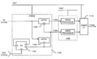
- C 3 MOS input circuitry 1100is a deserializer that receives a serial bit stream at a high frequency of, for example, 2 GHz.
- a 2 GHz input clock signal CLKis divided down to 1 GHz using a C 3 MOS flip-flop 1102 , such as the one shown in FIG. 8 , that is connected in a ⁇ 2 feedback configuration.
- the 1 GHz output of flip-flop 1102is then supplied to clock inputs of a pair of C 3 MOS latches 1104 and 1106 .
- Latches 1104 and 1106which may be of the type shown in FIG.
- block 11thus deserializes the input bit stream with its frequency halved to allow for the use of conventional CMOS logic to process the signals.
- the signals at the outputs of latches 1104 and 1106are applied to parallel processing circuitry 1108 that are implemented in conventional CMOS logic operating at 1 GHz.
- the reverseis performed at the output where a serializer 1110 receives the output signals from processing circuitry 1108 and serializes them using C 3 MOS logic.
- the final output signalis a bit stream with the original 2 GHz frequency. Circuit applications wherein this technique can be advantageously be employed include high speed single or multi-channel serial links in communication systems.
- this techniquedoubles the amount of the core signal processing circuitry.
- this part of the circuitis implemented in conventional CMOS logic, current dissipation is not increased by the doubling of the circuitry.
- CMOS logiccomplementary metal-oxide-semiconductor
- there can be more than one level of deserializingif further reduction in operating frequency is desired. That is, the frequency of the input signal can be divided down further by 4 or 8 or more if desired.
- the amount and size of the overall circuitryincreases in direct proportion to the number by which the input signal frequency is divided. For each application, therefore, there is an optimum number depending on the speed, power and area requirements.
- the combined C 3 MOS/CMOS circuit technique as shown in FIG. 11is employed in a transceiver of the type illustrated in FIG. 12 .
- the exemplary transceiver of FIG. 12is typically found along fiber optic channels in high speed telecommunication networks.
- the transceiverincludes at its input a photo detect and driver circuit 1200 that receives the input signal from the fiber optic channel.
- Circuit 1200converts fiber-optic signal to packets of data and supplies it to a clock data recovery (CDR) circuit 1202 .
- CDR circuit 1202recovers the clock and data signals that may be in the frequency range of about 2.5 GHz, or higher.
- Established telecommunication standardsrequire the transceiver to perform various functions, including data monitoring and error correction.
- the transceiveruses a demultiplexer 1204 which deserializes the 2.5 GHz data stream into, for example, 16 parallel signals having a frequency of about 155 MHz.
- An application specific integrated circuit (ASIC) 1206then performs the monitoring and error correction functions at the lower (155 MHz) frequency.
- a multiplexer and clock multiplication unit (CMU) 1208converts the parallel signals back into a single bit stream at 2.5 GHz. This signal is then retransmitted back onto the fiber optic channel by a laser drive 1212 .
- demultiplexer 1204ASIC 1206 and multiplexer and CMU 1208 on a single silicon die in a similar fashion as described in connection with the circuit of FIGS. 10 and 11 . That is, demultiplexer 1204 and multiplexer and CMU 1208 are implemented in C 3 MOS with ASIC 1206 implemented in conventional CMOS.
- circuit speedis further enhanced by using a higher supply voltage for the C 3 MOS circuitry than that which may be specified by the CMOS fabrication process.
- the ongoing advances in semiconductor fabrication technologycontinue to make smaller and faster devices possible.
- the smaller geometriesoften limit the voltage tolerance of the transistors. For example, while a thinner gate dielectric in an MOS transistor helps increase its speed of operation, the breakdown voltage at which damage may be caused to the transistor is also lowered. This reliability concern, as well as the desire to reduce power, have resulted in a downward trend in the permissible level of supply voltage for the modem sub-micron CMOS process.
- CMOS circuitry using C 3 MOS logicwhere there are more than two devices stacked between the two power supplies. That is, instead of the two transistors 102 and 104 in the conventional CMOS inverter shown in FIG. 1 , a typical C 3 MOS logic block such as buffer/inverter 200 of FIG. 2 has at least three devices, transistor 212 , transistor 202 (or 204 ) and resistor 206 (or 208 ) between Vcc and ground. Therefore, buffer/inverter 200 has less voltage across its transistors. It also has a more limited output voltage swing. Moreover, the low voltage differential signaling (LVDS) technique that is often employed in high speed circuits may have a common mode voltage requirement that, for the C 3 MOS circuitry, would be too high to meet when using a lower power supply voltage.
- LVDSlow voltage differential signaling
- a circuit according to this embodiment of the present inventioncan run the C 3 MOS portion off of a higher supply voltage of, e.g., 1.8 volts, while the CMOS portion of the circuit runs off of the prescribed 1.2 volt supply. Because the 1.8 volts is divided between at least one resistor and two transistors (as in the case of the C 3 MOS buffer/inverter of FIG. 2 ), the transistors do not experience excessive voltages between their terminals during operation. Also, because C 3 MOS circuitry typically processes signals with smaller swings, it can withstand the higher supply voltage. The higher power supply voltage greatly improves the speed of the circuit as well as its ability to meet the required LVDS output level.
- a pre-driver signal conditioning circuitis used to maximize the speed of C 3 MOS logic.
- the pre-driverdrives the inputs of a C 3 MOS buffer/level shifter of the type shown in FIG. 3 .
- To maximize the switching speed of the input transistors in the C 3 MOS stagetransistors M 1 and M 2 of FIG. 3 ), it is desirable to maintain these transistors operating in the saturation region.
- One way to accomplish thisis to reduce the common mode level of the differential input signal driving the gate terminals of transistors M 1 and M 2 . However, this would mean that with a lower power supply voltage at Vcc, the pre-driver voltage would have to be even lower.
- a pair of termination resistors RT 1 and RT 2connect across the input terminals INP and INN, and a voltage divider made of a pair of resistors Rb 1 and Rb 2 set the common mode bias voltage for the input signal.
- Other implementationsare possible.
- the dual power supply embodiment of the present inventioncan be implemented in a number of ways.
- two separate supply voltagescan be applied externally. The higher voltage would be applied to the C 3 MOS logic circuitry and the lower voltage to the conventional CMOS logic circuitry. This embodiment would require two external pins for the chip.
- An alternative embodimentreceives only one power supply voltage and generates the other on-chip. That is, a circuit could operate with two different supply voltages Vcc 1 for C 3 MOS logic circuitry and Vcc 2 for conventional CMOS logic circuitry.
- a voltage generatorreceives Vcc 1 and generates the second supply voltage Vcc 2 for use with conventional CMOS logic circuitry.
- a variety of circuit implementationsare known for a voltage generator.
- One example of a circuit implementation for a voltage generatorincludes a voltage divider made up of resistors Rd 1 and Rd 2 that connect between the first power supply voltage Vcc 1 and ground. Resistors Rd 1 and Rd 2 are sized to generate the desired second voltage level Vcc 2 ′. An amplifier connected in a unity gain configuration provides a buffer between the divider and the output Vcc 2 that is to be used by the conventional CMOS logic circuitry.
- the present inventionprovides various circuit techniques for implementing ultra high speed circuits using current-controlled CMOS (C 3 MOS) logic fabricated in conventional CMOS process technology.
- C 3 MOScurrent-controlled CMOS
- An entire family of logic elements including inverter/buffers, level shifters, NAND, NOR, XOR gates, latches, flip-flops and the likehave been developed using C 3 MOS according to the present invention.
- the present inventionadvantageously combines high speed C 3 MOS logic with low power conventional CMOS logic.
- circuitssuch as transceivers along fiber optic channels can be fabricated on a single chip where the ultra-high speed portions of the circuit utilize C 3 MOS and the relatively lower speed parts of the circuit use conventional CMOS logic.
- the C 3 MOS logic circuitryreceives a first power supply voltage that is higher than the power supply voltage used by the conventional CMOS logic circuitry.
Landscapes
- Engineering & Computer Science (AREA)
- Power Engineering (AREA)
- Physics & Mathematics (AREA)
- Computer Hardware Design (AREA)
- Computing Systems (AREA)
- General Engineering & Computer Science (AREA)
- Mathematical Physics (AREA)
- Logic Circuits (AREA)
Abstract
Description
Claims (19)
Priority Applications (1)
| Application Number | Priority Date | Filing Date | Title |
|---|---|---|---|
| US10/177,031US6911855B2 (en) | 1999-06-28 | 2002-06-21 | Current-controlled CMOS circuit using higher voltage supply in low voltage CMOS process |
Applications Claiming Priority (3)
| Application Number | Priority Date | Filing Date | Title |
|---|---|---|---|
| US14135599P | 1999-06-28 | 1999-06-28 | |
| US09/484,856US6424194B1 (en) | 1999-06-28 | 2000-01-18 | Current-controlled CMOS logic family |
| US10/177,031US6911855B2 (en) | 1999-06-28 | 2002-06-21 | Current-controlled CMOS circuit using higher voltage supply in low voltage CMOS process |
Related Parent Applications (1)
| Application Number | Title | Priority Date | Filing Date |
|---|---|---|---|
| US09/484,856Continuation-In-PartUS6424194B1 (en) | 1999-06-28 | 2000-01-18 | Current-controlled CMOS logic family |
Publications (2)
| Publication Number | Publication Date |
|---|---|
| US20030067337A1 US20030067337A1 (en) | 2003-04-10 |
| US6911855B2true US6911855B2 (en) | 2005-06-28 |
Family
ID=46280773
Family Applications (1)
| Application Number | Title | Priority Date | Filing Date |
|---|---|---|---|
| US10/177,031Expired - LifetimeUS6911855B2 (en) | 1999-06-28 | 2002-06-21 | Current-controlled CMOS circuit using higher voltage supply in low voltage CMOS process |
Country Status (1)
| Country | Link |
|---|---|
| US (1) | US6911855B2 (en) |
Cited By (18)
| Publication number | Priority date | Publication date | Assignee | Title |
|---|---|---|---|---|
| US20050015638A1 (en)* | 2001-07-19 | 2005-01-20 | Bo Zhang | Synchronous data serialization circuit |
| US20050040873A1 (en)* | 2003-08-20 | 2005-02-24 | Tooru Wada | Semiconductor integrated circuit |
| US20060241877A1 (en)* | 2005-04-08 | 2006-10-26 | Kabushiki Kaisha Toshiba | Semiconductor integrated circuit and method of testing delay thereof |
| US20070170966A1 (en)* | 1999-06-28 | 2007-07-26 | Broadcom Corporation, A California Corporation | Current-controlled CMOS logic family |
| US7545834B1 (en) | 2006-01-10 | 2009-06-09 | Pericom Semiconductor Corp. | Multiple channel switch using differential de-mux amplifier and differential mux equalizer |
| US7849208B2 (en) | 2002-08-30 | 2010-12-07 | Broadcom Corporation | System and method for TCP offload |
| US7912064B2 (en) | 2002-08-30 | 2011-03-22 | Broadcom Corporation | System and method for handling out-of-order frames |
| US7934021B2 (en) | 2002-08-29 | 2011-04-26 | Broadcom Corporation | System and method for network interfacing |
| US8116203B2 (en) | 2001-07-23 | 2012-02-14 | Broadcom Corporation | Multiple virtual channels for use in network devices |
| US8135016B2 (en) | 2002-03-08 | 2012-03-13 | Broadcom Corporation | System and method for identifying upper layer protocol message boundaries |
| US8180928B2 (en) | 2002-08-30 | 2012-05-15 | Broadcom Corporation | Method and system for supporting read operations with CRC for iSCSI and iSCSI chimney |
| US20120299626A1 (en)* | 2011-05-26 | 2012-11-29 | Semiconductor Energy Laboratory Co., Ltd. | Divider circuit and semiconductor device using the same |
| US8402142B2 (en) | 2002-08-30 | 2013-03-19 | Broadcom Corporation | System and method for TCP/IP offload independent of bandwidth delay product |
| US20140009000A1 (en)* | 2012-07-03 | 2014-01-09 | Harish Naga Venkata | Current conveyor circuit |
| US8750320B2 (en) | 1997-01-23 | 2014-06-10 | Broadcom Corporation | Fibre channel arbitrated loop bufferless switch circuitry to increase bandwidth without significant increase in cost |
| US8798091B2 (en) | 1998-11-19 | 2014-08-05 | Broadcom Corporation | Fibre channel arbitrated loop bufferless switch circuitry to increase bandwidth without significant increase in cost |
| US9628077B2 (en)* | 2015-03-04 | 2017-04-18 | Qualcomm Incorporated | Dual power swing pipeline design with separation of combinational and sequential logics |
| US10840907B1 (en) | 2019-11-19 | 2020-11-17 | Honeywell International Inc. | Source-coupled logic with reference controlled inputs |
Families Citing this family (5)
| Publication number | Priority date | Publication date | Assignee | Title |
|---|---|---|---|---|
| US7405593B2 (en)* | 2005-10-28 | 2008-07-29 | Fujitsu Limited | Systems and methods for transmitting signals across integrated circuit chips |
| JP5057828B2 (en)* | 2007-04-16 | 2012-10-24 | 株式会社ジャパンディスプレイイースト | Display device |
| US7683673B2 (en)* | 2007-04-24 | 2010-03-23 | National Semiconductor Corporation | Stacked differential signal transmission circuitry |
| JP5191719B2 (en)* | 2007-10-31 | 2013-05-08 | 株式会社日立製作所 | Wireless IC tag system and wireless IC tag operating method |
| US11863181B2 (en)* | 2021-09-22 | 2024-01-02 | Nxp Usa, Inc. | Level-shifter |
Citations (165)
| Publication number | Priority date | Publication date | Assignee | Title |
|---|---|---|---|---|
| US4333020A (en) | 1979-05-23 | 1982-06-01 | Motorola, Inc. | MOS Latch circuit |
| US4395774A (en) | 1981-01-12 | 1983-07-26 | National Semiconductor Corporation | Low power CMOS frequency divider |
| US4449248A (en) | 1982-02-01 | 1984-05-15 | General Electric Company | Battery saving radio circuit and system |
| US4519068A (en) | 1983-07-11 | 1985-05-21 | Motorola, Inc. | Method and apparatus for communicating variable length messages between a primary station and remote stations of a data communications system |
| US4545023A (en) | 1980-11-14 | 1985-10-01 | Engineering Project Development Limited | Hand-held computer |
| US4599526A (en) | 1983-05-13 | 1986-07-08 | At&T Bell Laboratories | Clocked latching circuit |
| US4649293A (en) | 1984-11-09 | 1987-03-10 | U.S. Philips Corporation | Clocked comparator |
| US4680787A (en) | 1984-11-21 | 1987-07-14 | Motorola, Inc. | Portable radiotelephone vehicular converter and remote handset |
| US4727309A (en) | 1987-01-22 | 1988-02-23 | Intel Corporation | Current difference current source |
| US4731796A (en) | 1984-10-25 | 1988-03-15 | Stc, Plc | Multi-mode radio transceiver |
| US4737975A (en) | 1984-09-18 | 1988-04-12 | Metrofone, Inc. | Programmable system for interfacing a standard telephone set with a radio transceiver |
| US4761822A (en) | 1985-08-23 | 1988-08-02 | Libera Developments Ltd. | Burst-mode two-way radio communications system |
| US4777657A (en) | 1987-04-01 | 1988-10-11 | Iss Engineering, Inc. | Computer controlled broadband receiver |
| JPS63280517A (en) | 1987-05-13 | 1988-11-17 | Nec Corp | Logic circuit |
| US4794649A (en) | 1986-05-06 | 1988-12-27 | Nec Corporation | Radio communication system with power saving disablement prior to call handling processes |
| US4804954A (en) | 1987-04-30 | 1989-02-14 | Motorola, Inc. | Battery saving method for portable communications receivers |
| US4806796A (en) | 1988-03-28 | 1989-02-21 | Motorola, Inc. | Active load for emitter coupled logic gate |
| US4807282A (en) | 1985-12-30 | 1989-02-21 | International Business Machines Corp. | Programmable P/C compatible communications card |
| US4817115A (en) | 1987-02-27 | 1989-03-28 | Telxon Corporation | Encoding and decoding system for electronic data communication system |
| US4850009A (en) | 1986-05-12 | 1989-07-18 | Clinicom Incorporated | Portable handheld terminal including optical bar code reader and electromagnetic transceiver means for interactive wireless communication with a base communications station |
| US4890832A (en) | 1982-10-13 | 1990-01-02 | Sharp Kabushiki Kaisha | Compact electronic apparatus with removable processing units |
| US4894792A (en) | 1988-09-30 | 1990-01-16 | Tandy Corporation | Portable computer with removable and replaceable add-on modules |
| US4916441A (en) | 1988-09-19 | 1990-04-10 | Clinicom Incorporated | Portable handheld terminal |
| US4964121A (en) | 1989-08-30 | 1990-10-16 | Motorola, Inc. | Battery saver for a TDM system |
| US4969206A (en) | 1989-07-18 | 1990-11-06 | Phyle Industries Limited | Portable data collection device with RF transmission |
| US4970406A (en) | 1987-12-30 | 1990-11-13 | Gazelle Microcircuits, Inc. | Resettable latch circuit |
| US4977611A (en) | 1987-02-20 | 1990-12-11 | Nec Corporation | Portable radio apparatus having battery saved channel scanning function |
| US4995099A (en) | 1988-12-01 | 1991-02-19 | Motorola, Inc. | Power conservation method and apparatus for a portion of a predetermined signal |
| US5008879A (en) | 1988-11-14 | 1991-04-16 | Datapoint Corporation | LAN with interoperative multiple operational capabilities |
| US5025486A (en) | 1988-12-09 | 1991-06-18 | Dallas Semiconductor Corporation | Wireless communication system with parallel polling |
| US5029183A (en) | 1989-06-29 | 1991-07-02 | Symbol Technologies, Inc. | Packet data communication network |
| US5031231A (en) | 1988-09-26 | 1991-07-09 | Nec Corporation | Mobile telephone station with power saving circuit |
| US5033109A (en) | 1988-07-01 | 1991-07-16 | Mitsubishi Denki Kabushiki Kaisha | Pocket transceiver |
| US5041740A (en) | 1990-04-30 | 1991-08-20 | Motorola, Inc. | Parallel clocked latch |
| US5055659A (en) | 1990-02-06 | 1991-10-08 | Amtech Technology Corp. | High speed system for reading and writing data from and into remote tags |
| US5055660A (en) | 1988-06-16 | 1991-10-08 | Avicom International, Inc. | Portable transaction monitoring unit for transaction monitoring and security control systems |
| US5079452A (en) | 1990-06-29 | 1992-01-07 | Digital Equipment Corporation | High speed ECL latch with clock enable |
| US5081402A (en) | 1991-02-22 | 1992-01-14 | Comfortex Corporation | Low power consumption wireless data transmission and control system |
| US5087099A (en) | 1988-09-02 | 1992-02-11 | Stolar, Inc. | Long range multiple point wireless control and monitoring system |
| US5115151A (en) | 1990-06-08 | 1992-05-19 | Western Digital Corporation | Triple comparator circuit |
| US5117501A (en) | 1988-08-08 | 1992-05-26 | General Electric Company | Dynamic regrouping in a trunked radio communications system |
| US5119502A (en) | 1990-08-30 | 1992-06-02 | Telefonaktiebolaget L M Ericsson | Periodic system ordered rescan in a cellular communication system |
| US5121408A (en) | 1989-10-16 | 1992-06-09 | Hughes Aircraft Company | Synchronization for entry to a network in a frequency hopping communication system |
| US5123029A (en) | 1991-06-21 | 1992-06-16 | International Business Machines Corporation | Broadcast-initiated bipartite frame multi-access protocol |
| US5128938A (en) | 1989-03-03 | 1992-07-07 | Motorola, Inc. | Energy saving protocol for a communication system |
| US5134347A (en) | 1991-02-22 | 1992-07-28 | Comfortex Corporation | Low power consumption wireless data transmission and control system |
| US5142573A (en) | 1990-02-08 | 1992-08-25 | Oki Electric Industry Co., Ltd. | Telephone apparatus for radio communication with an adaptor |
| US5150361A (en) | 1989-01-23 | 1992-09-22 | Motorola, Inc. | Energy saving protocol for a TDM radio |
| US5152006A (en) | 1991-02-25 | 1992-09-29 | Motorola, Inc. | Receiver controller method and apparatus |
| US5153878A (en) | 1989-12-11 | 1992-10-06 | Motorola Inc. | Radio data communications system with diverse signaling capability |
| US5175870A (en) | 1988-12-23 | 1992-12-29 | U.S. Philips Corporation | Power economising in multiple user radio systems |
| US5177378A (en) | 1990-05-08 | 1993-01-05 | Kabushiki Kaisha Toshiba | Source-coupled FET logic circuit |
| US5179721A (en) | 1990-11-05 | 1993-01-12 | Motorola Inc. | Method for inter operation of a cellular communication system and a trunking communication system |
| US5181200A (en) | 1990-10-29 | 1993-01-19 | International Business Machines Corporation | Handoff method and apparatus for mobile wireless workstation |
| US5196805A (en) | 1992-01-31 | 1993-03-23 | Motorola, Inc. | Distributed differential amplifier arrangement |
| US5216295A (en) | 1991-08-30 | 1993-06-01 | General Instrument Corp. | Current mode logic circuits employing IGFETS |
| US5230084A (en) | 1990-12-06 | 1993-07-20 | Motorola, Inc. | Selective call receiver having extended battery saving capability |
| US5239662A (en) | 1986-09-15 | 1993-08-24 | Norand Corporation | System including multiple device communications controller which coverts data received from two different customer transaction devices each using different communications protocols into a single communications protocol |
| US5241691A (en) | 1990-03-09 | 1993-08-31 | U.S. Philips Corporation | Method of optimizing the transmission of idle beacon messages and a communications system using the method |
| US5241542A (en) | 1991-08-23 | 1993-08-31 | International Business Machines Corporation | Battery efficient operation of scheduled access protocol |
| US5247656A (en) | 1989-06-01 | 1993-09-21 | Matsushita Electric Industrial Co., Ltd. | Method and apparatus for controlling a clock signal |
| US5249220A (en) | 1991-04-18 | 1993-09-28 | Rts Electronics, Inc. | Handheld facsimile and alphanumeric message transceiver operating over telephone or wireless networks |
| US5249302A (en) | 1987-10-09 | 1993-09-28 | Motorola, Inc. | Mixed-mode transceiver system |
| US5265238A (en) | 1991-01-25 | 1993-11-23 | International Business Machines Corporation | Automatic device configuration for dockable portable computers |
| US5265270A (en) | 1990-10-31 | 1993-11-23 | Motorola, Inc. | Method and apparatus for providing power conservation in a communication system |
| US5274666A (en) | 1991-10-16 | 1993-12-28 | Telephonics Corporation | Wireless communication system |
| US5276680A (en) | 1991-04-11 | 1994-01-04 | Telesystems Slw Inc. | Wireless coupling of devices to wired network |
| US5278831A (en) | 1991-07-09 | 1994-01-11 | U.S. Philips Corporation | Information transmission system |
| US5289469A (en) | 1991-01-17 | 1994-02-22 | Kabushiki Kaisha Toshiba | Communication control unit with lower layer protocol control and higher layer protocol control |
| US5289055A (en) | 1992-11-17 | 1994-02-22 | At&T Bell Laboratories | Digital ECL bipolar logic gates suitable for low-voltage operation |
| US5291516A (en) | 1991-05-13 | 1994-03-01 | Omnipoint Data Company, Inc. | Dual mode transmitter and receiver |
| US5293639A (en) | 1991-08-09 | 1994-03-08 | Motorola, Inc. | Reduction of power consumption in a portable communication unit |
| US5296849A (en) | 1990-10-25 | 1994-03-22 | Nec Corporation | Pager receiver for enabling to omit power-on signal for receiving synchronization code in pager signal |
| US5297144A (en) | 1991-01-22 | 1994-03-22 | Spectrix Corporation | Reservation-based polling protocol for a wireless data communications network |
| US5301196A (en) | 1992-03-16 | 1994-04-05 | International Business Machines Corporation | Half-speed clock recovery and demultiplexer circuit |
| US5323392A (en) | 1991-03-13 | 1994-06-21 | International Business Machines Corporation | Adaptation device and method for efficient interconnection of data processing devices and networks |
| US5331509A (en) | 1992-06-29 | 1994-07-19 | Cordata, Inc. | Modular notebook computer having a planar array of module bays and a pivotally attached flat-panel display |
| US5345449A (en) | 1989-07-07 | 1994-09-06 | Inmos Limited | Clock generation |
| US5349649A (en) | 1991-04-22 | 1994-09-20 | Kabushiki Kaisha Toshiba | Portable electronic device supporting multi-protocols |
| US5361397A (en) | 1991-08-26 | 1994-11-01 | Motorola, Inc. | Communication device and system capable of automatic programmable energizing |
| US5363121A (en) | 1990-06-29 | 1994-11-08 | International Business Machines Corporation | Multiple protocol communication interface for distributed transaction processing |
| US5373506A (en) | 1990-11-26 | 1994-12-13 | Motorola Inc. | Method and apparatus for paging in a communication system |
| US5373149A (en) | 1993-02-01 | 1994-12-13 | At&T Bell Laboratories | Folding electronic card assembly |
| US5390206A (en) | 1991-10-01 | 1995-02-14 | American Standard Inc. | Wireless communication system for air distribution system |
| US5392023A (en) | 1991-09-06 | 1995-02-21 | Motorola, Inc. | Data communication system with automatic power control |
| US5396128A (en)* | 1993-09-13 | 1995-03-07 | Motorola, Inc. | Output circuit for interfacing integrated circuits having different power supply potentials |
| US5399920A (en)* | 1993-11-09 | 1995-03-21 | Texas Instruments Incorporated | CMOS driver which uses a higher voltage to compensate for threshold loss of the pull-up NFET |
| US5406615A (en) | 1993-08-04 | 1995-04-11 | At&T Corp. | Multi-band wireless radiotelephone operative in a plurality of air interface of differing wireless communications systems |
| US5406643A (en) | 1993-02-11 | 1995-04-11 | Motorola, Inc. | Method and apparatus for selecting between a plurality of communication paths |
| US5418837A (en) | 1993-07-30 | 1995-05-23 | Ericsson-Ge Mobile Communications Inc. | Method and apparatus for upgrading cellular mobile telephones |
| US5420529A (en) | 1994-05-19 | 1995-05-30 | Northern Telecom Limited | Current steering switch and hybrid BiCMOS multiplexer with CMOS commutation signal and CML/ECL data signals |
| US5423002A (en) | 1992-04-20 | 1995-06-06 | 3Com Corporation | System for extending network resources to remote networks |
| US5426637A (en) | 1992-12-14 | 1995-06-20 | International Business Machines Corporation | Methods and apparatus for interconnecting local area networks with wide area backbone networks |
| US5428636A (en) | 1993-05-03 | 1995-06-27 | Norand Corporation | Radio frequency local area network |
| US5430845A (en) | 1990-06-07 | 1995-07-04 | Unisys Corporation | Peripheral device interface for dynamically selecting boot disk device driver |
| US5434518A (en) | 1992-10-02 | 1995-07-18 | National Semiconductor Corporation | ECL-to-BICOMS/CMOS translator |
| US5438329A (en) | 1993-06-04 | 1995-08-01 | M & Fc Holding Company, Inc. | Duplex bi-directional multi-mode remote instrument reading and telemetry system |
| US5440560A (en) | 1991-12-24 | 1995-08-08 | Rypinski; Chandos A. | Sleep mode and contention resolution within a common channel medium access method |
| US5457412A (en) | 1992-11-17 | 1995-10-10 | Hitachi, Ltd. | Semiconductor integrated circuit device including input circuitry to permit operation of a Bi-CMOS memory with ECL level input signals |
| US5459412A (en) | 1993-07-01 | 1995-10-17 | National Semiconductor Corporation | BiCMOS circuit for translation of ECL logic levels to MOS logic levels |
| US5465081A (en) | 1990-03-03 | 1995-11-07 | Cedar-Dell Limited | Multicomponent wireless system with periodic shutdown of transmitting and receiving modes |
| US5481265A (en) | 1989-11-22 | 1996-01-02 | Russell; David C. | Ergonomic customizeable user/computer interface devices |
| US5481562A (en) | 1989-11-03 | 1996-01-02 | Microcom Systems, Inc. | Multi-mode modem and data transmission method |
| US5510734A (en) | 1994-06-14 | 1996-04-23 | Nec Corporation | High speed comparator having two differential amplifier stages and latch stage |
| US5510748A (en) | 1994-01-18 | 1996-04-23 | Vivid Semiconductor, Inc. | Integrated circuit having different power supplies for increased output voltage range while retaining small device geometries |
| US5521530A (en) | 1994-08-31 | 1996-05-28 | Oki Semiconductor America, Inc. | Efficient method and resulting structure for integrated circuits with flexible I/O interface and power supply voltages |
| US5533029A (en) | 1993-11-12 | 1996-07-02 | Pacific Communication Sciences, Inc. | Cellular digital packet data mobile data base station |
| US5535373A (en) | 1991-11-27 | 1996-07-09 | International Business Machines Corporation | Protocol-to-protocol translator for interfacing disparate serial network nodes to a common parallel switching network |
| US5548230A (en) | 1994-05-31 | 1996-08-20 | Pmc-Sierra, Inc. | High-speed CMOS pseudo-ECL output driver |
| US5559464A (en)* | 1993-07-06 | 1996-09-24 | Seiko Epson Corporation | Signal voltage level conversion circuit and output buffer circuit |
| US5576644A (en) | 1994-06-10 | 1996-11-19 | International Business Machines Corporation | Fast edge triggered self-resetting CMOS receiver with parallel L1/L2 (master/slave) latch |
| US5579487A (en) | 1992-10-02 | 1996-11-26 | Teletransaction, Inc. | Portable work slate computer with multiple docking positions for interchangeably receiving removable modules |
| US5584048A (en) | 1990-08-17 | 1996-12-10 | Motorola, Inc. | Beacon based packet radio standby energy saver |
| US5600267A (en) | 1994-06-24 | 1997-02-04 | Cypress Semiconductor Corporation | Apparatus for a programmable CML to CMOS translator for power/speed adjustment |
| US5606268A (en) | 1993-03-24 | 1997-02-25 | Apple Computer, Inc. | Differential to single-ended CMOS converter |
| US5625308A (en) | 1995-06-08 | 1997-04-29 | Mitsubishi Denki Kabushiki Kaisha | Two input-two output differential latch circuit |
| US5628055A (en) | 1993-03-04 | 1997-05-06 | Telefonaktiebolaget L M Ericsson Publ | Modular radio communications system |
| US5630061A (en) | 1993-04-19 | 1997-05-13 | International Business Machines Corporation | System for enabling first computer to communicate over switched network with second computer located within LAN by using media access control driver in different modes |
| US5640356A (en) | 1995-12-29 | 1997-06-17 | Cypress Semiconductor Corp. | Two-stage differential sense amplifier with positive feedback in the first and second stages |
| US5675584A (en) | 1994-06-06 | 1997-10-07 | Sun Microsystems, Inc. | High speed serial link for fully duplexed data communication |
| US5680633A (en) | 1990-01-18 | 1997-10-21 | Norand Corporation | Modular, portable data processing terminal for use in a radio frequency communication network |
| US5724361A (en) | 1996-03-12 | 1998-03-03 | Lsi Logic Corporation | High performance n:1 multiplexer with overlap control of multi-phase clocks |
| US5732346A (en) | 1993-06-17 | 1998-03-24 | Research In Motion Limited | Translation and connection device for radio frequency point of sale transaction systems |
| US5740366A (en) | 1991-10-01 | 1998-04-14 | Norand Corporation | Communication network having a plurality of bridging nodes which transmit a beacon to terminal nodes in power saving state that it has messages awaiting delivery |
| US5744366A (en) | 1992-05-01 | 1998-04-28 | Trustees Of The University Of Pennsylvania | Mesoscale devices and methods for analysis of motile cells |
| US5767699A (en) | 1996-05-28 | 1998-06-16 | Sun Microsystems, Inc. | Fully complementary differential output driver for high speed digital communications |
| US5796727A (en) | 1993-04-30 | 1998-08-18 | International Business Machines Corporation | Wide-area wireless lan access |
| US5798658A (en) | 1995-06-15 | 1998-08-25 | Werking; Paul M. | Source-coupled logic with reference controlled inputs |
| US5821809A (en) | 1996-05-23 | 1998-10-13 | International Business Machines Corporation | CMOS high-speed differential to single-ended converter circuit |
| US5839051A (en) | 1989-03-17 | 1998-11-17 | Technophone Limited | Host radio telephone to directly access a handset NAM through a connecter without requiring the handset controller to be employed |
| US5877642A (en) | 1995-11-17 | 1999-03-02 | Nec Corporation | Latch circuit for receiving small amplitude signals |
| US5892382A (en) | 1997-03-25 | 1999-04-06 | Mitsubishi Denki Kabushiki Kaisha | Current mode logic circuit, source follower circuit and flip flop circuit |
| US5903176A (en) | 1996-09-04 | 1999-05-11 | Litton Systems, Inc. | Clock circuit for generating a high resolution output from a low resolution clock |
| US5905386A (en) | 1996-01-02 | 1999-05-18 | Pmc-Sierra Ltd. | CMOS SONET/ATM receiver suitable for use with pseudo ECL and TTL signaling environments |
| US5940771A (en) | 1991-05-13 | 1999-08-17 | Norand Corporation | Network supporting roaming, sleeping terminals |
| US5945858A (en) | 1997-03-31 | 1999-08-31 | Nec Corporation | Clocked flip flop circuit with built-in clock controller and frequency divider using the same |
| US5945863A (en) | 1997-06-18 | 1999-08-31 | Applied Micro Circuits Corporation | Analog delay circuit |
| US5945847A (en) | 1997-05-20 | 1999-08-31 | Lucent Technologies | Distributed amplifier logic designs |
| US5952847A (en)* | 1996-06-25 | 1999-09-14 | Actel Corporation | Multiple logic family compatible output driver |
| US5969556A (en) | 1997-03-05 | 1999-10-19 | Mitsubishi Denki Kabushiki Kaisha | Flip-flop circuit, parallel-serial converting circuit, and latch circuit |
| US6002279A (en) | 1997-10-24 | 1999-12-14 | G2 Networks, Inc. | Clock recovery circuit |
| US6014041A (en) | 1997-09-26 | 2000-01-11 | Intel Corporation | Differential current switch logic gate |
| US6014705A (en) | 1991-10-01 | 2000-01-11 | Intermec Ip Corp. | Modular portable data processing terminal having a higher layer and lower layer partitioned communication protocol stack for use in a radio frequency communications network |
| US6028454A (en) | 1997-04-11 | 2000-02-22 | The University Of Waterloo | Dynamic current mode logic family |
| US6037841A (en) | 1997-10-07 | 2000-03-14 | Applied Micro Circuits Corporation | Impedance matched CMOS transimpedance amplifier for high-speed fiber optic communications |
| US6038254A (en) | 1996-06-07 | 2000-03-14 | International Business Machines Corporation | Adaptive filtering method and apparatus to compensate for a frequency difference between two clock sources |
| US6037842A (en) | 1998-04-21 | 2000-03-14 | Applied Micro Circuits Corporation | Complementary metal-oxide semiconductor voltage controlled oscillator (CMOS VCO) |
| US6061747A (en) | 1997-10-16 | 2000-05-09 | Lsi Logic Corporation | System for sending data from-and-to a computer monitor using a high speed serial line |
| US6064229A (en)* | 1998-03-26 | 2000-05-16 | Lucent Technologies Inc. | Voltage translating buffer based on low voltage technology |
| US6081162A (en) | 1999-06-17 | 2000-06-27 | Intel Corporation | Robust method and apparatus for providing a digital single-ended output from a differential input |
| US6094074A (en) | 1998-07-16 | 2000-07-25 | Seiko Epson Corporation | High speed common mode logic circuit |
| US6099100A (en)* | 1997-07-15 | 2000-08-08 | Lg Semicon Co., Ltd. | CMOS digital level shift circuit |
| US6111425A (en)* | 1998-10-15 | 2000-08-29 | International Business Machines Corporation | Very low power logic circuit family with enhanced noise immunity |
| US6114843A (en) | 1998-08-18 | 2000-09-05 | Xilinx, Inc. | Voltage down converter for multiple voltage levels |
| US6188339B1 (en) | 1998-01-23 | 2001-02-13 | Fuji Photo Film Co., Ltd. | Differential multiplexer and differential logic circuit |
| US6194950B1 (en) | 1997-08-28 | 2001-02-27 | Lucent Technologies Inc. | High-speed CMOS multiplexer |
| US6222380B1 (en) | 1998-06-15 | 2001-04-24 | International Business Machines Corporation | High speed parallel/serial link for data communication |
| US6232844B1 (en) | 1999-05-28 | 2001-05-15 | Vitesse Semiconductor Corporation | Controlled orthogonal current oscillator with ranging |
| US6242949B1 (en)* | 1998-06-26 | 2001-06-05 | Micron Technology, Inc. | Digital voltage translator and its method of operation |
| US6259312B1 (en) | 1998-03-11 | 2001-07-10 | Nokia Mobile Phones Limited | Circuit arrangement for adjusting the impedance of a differential active component |
| US6265898B1 (en) | 1998-07-13 | 2001-07-24 | Texas Instruments Incorporated | Current mode logic gates for low-voltage high speed applications |
| US6310501B1 (en) | 1998-11-27 | 2001-10-30 | Nec Corporation | Latch circuit for latching data at an edge of a clock signal |
| US6374311B1 (en) | 1991-10-01 | 2002-04-16 | Intermec Ip Corp. | Communication network having a plurality of bridging nodes which transmit a beacon to terminal nodes in power saving state that it has messages awaiting delivery |
| US6424194B1 (en) | 1999-06-28 | 2002-07-23 | Broadcom Corporation | Current-controlled CMOS logic family |
| US6463092B1 (en) | 1998-09-10 | 2002-10-08 | Silicon Image, Inc. | System and method for sending and receiving data signals over a clock signal line |
Family Cites Families (2)
| Publication number | Priority date | Publication date | Assignee | Title |
|---|---|---|---|---|
| US4737795A (en)* | 1986-07-25 | 1988-04-12 | General Motors Corporation | Vehicle roof mounted slot antenna with AM and FM grounding |
| US5535029A (en)* | 1995-01-12 | 1996-07-09 | The United States Of America As Represented By The Secretary Of The Air Force | Spatial light modulator having amplitude coupled with binary phase mode |
- 2002
- 2002-06-21USUS10/177,031patent/US6911855B2/ennot_activeExpired - Lifetime
Patent Citations (168)
| Publication number | Priority date | Publication date | Assignee | Title |
|---|---|---|---|---|
| US4333020A (en) | 1979-05-23 | 1982-06-01 | Motorola, Inc. | MOS Latch circuit |
| US4545023A (en) | 1980-11-14 | 1985-10-01 | Engineering Project Development Limited | Hand-held computer |
| US4395774A (en) | 1981-01-12 | 1983-07-26 | National Semiconductor Corporation | Low power CMOS frequency divider |
| US4449248A (en) | 1982-02-01 | 1984-05-15 | General Electric Company | Battery saving radio circuit and system |
| US4890832A (en) | 1982-10-13 | 1990-01-02 | Sharp Kabushiki Kaisha | Compact electronic apparatus with removable processing units |
| US4599526A (en) | 1983-05-13 | 1986-07-08 | At&T Bell Laboratories | Clocked latching circuit |
| US4519068A (en) | 1983-07-11 | 1985-05-21 | Motorola, Inc. | Method and apparatus for communicating variable length messages between a primary station and remote stations of a data communications system |
| US4737975A (en) | 1984-09-18 | 1988-04-12 | Metrofone, Inc. | Programmable system for interfacing a standard telephone set with a radio transceiver |
| US4731796A (en) | 1984-10-25 | 1988-03-15 | Stc, Plc | Multi-mode radio transceiver |
| US4649293A (en) | 1984-11-09 | 1987-03-10 | U.S. Philips Corporation | Clocked comparator |
| US4680787A (en) | 1984-11-21 | 1987-07-14 | Motorola, Inc. | Portable radiotelephone vehicular converter and remote handset |
| US4761822A (en) | 1985-08-23 | 1988-08-02 | Libera Developments Ltd. | Burst-mode two-way radio communications system |
| US4807282A (en) | 1985-12-30 | 1989-02-21 | International Business Machines Corp. | Programmable P/C compatible communications card |
| US4794649A (en) | 1986-05-06 | 1988-12-27 | Nec Corporation | Radio communication system with power saving disablement prior to call handling processes |
| US4850009A (en) | 1986-05-12 | 1989-07-18 | Clinicom Incorporated | Portable handheld terminal including optical bar code reader and electromagnetic transceiver means for interactive wireless communication with a base communications station |
| US5239662A (en) | 1986-09-15 | 1993-08-24 | Norand Corporation | System including multiple device communications controller which coverts data received from two different customer transaction devices each using different communications protocols into a single communications protocol |
| US4727309A (en) | 1987-01-22 | 1988-02-23 | Intel Corporation | Current difference current source |
| US4977611A (en) | 1987-02-20 | 1990-12-11 | Nec Corporation | Portable radio apparatus having battery saved channel scanning function |
| US4817115A (en) | 1987-02-27 | 1989-03-28 | Telxon Corporation | Encoding and decoding system for electronic data communication system |
| US4777657A (en) | 1987-04-01 | 1988-10-11 | Iss Engineering, Inc. | Computer controlled broadband receiver |
| US4804954A (en) | 1987-04-30 | 1989-02-14 | Motorola, Inc. | Battery saving method for portable communications receivers |
| JPS63280517A (en) | 1987-05-13 | 1988-11-17 | Nec Corp | Logic circuit |
| US5249302A (en) | 1987-10-09 | 1993-09-28 | Motorola, Inc. | Mixed-mode transceiver system |
| US4970406A (en) | 1987-12-30 | 1990-11-13 | Gazelle Microcircuits, Inc. | Resettable latch circuit |
| US4806796A (en) | 1988-03-28 | 1989-02-21 | Motorola, Inc. | Active load for emitter coupled logic gate |
| US5055660A (en) | 1988-06-16 | 1991-10-08 | Avicom International, Inc. | Portable transaction monitoring unit for transaction monitoring and security control systems |
| US5033109A (en) | 1988-07-01 | 1991-07-16 | Mitsubishi Denki Kabushiki Kaisha | Pocket transceiver |
| US5117501A (en) | 1988-08-08 | 1992-05-26 | General Electric Company | Dynamic regrouping in a trunked radio communications system |
| US5087099A (en) | 1988-09-02 | 1992-02-11 | Stolar, Inc. | Long range multiple point wireless control and monitoring system |
| US4916441A (en) | 1988-09-19 | 1990-04-10 | Clinicom Incorporated | Portable handheld terminal |
| US5031231A (en) | 1988-09-26 | 1991-07-09 | Nec Corporation | Mobile telephone station with power saving circuit |
| US4894792A (en) | 1988-09-30 | 1990-01-16 | Tandy Corporation | Portable computer with removable and replaceable add-on modules |
| US5008879B1 (en) | 1988-11-14 | 2000-05-30 | Datapoint Corp | Lan with interoperative multiple operational capabilities |
| US5008879A (en) | 1988-11-14 | 1991-04-16 | Datapoint Corporation | LAN with interoperative multiple operational capabilities |
| US4995099A (en) | 1988-12-01 | 1991-02-19 | Motorola, Inc. | Power conservation method and apparatus for a portion of a predetermined signal |
| US5025486A (en) | 1988-12-09 | 1991-06-18 | Dallas Semiconductor Corporation | Wireless communication system with parallel polling |
| US5175870A (en) | 1988-12-23 | 1992-12-29 | U.S. Philips Corporation | Power economising in multiple user radio systems |
| US5150361A (en) | 1989-01-23 | 1992-09-22 | Motorola, Inc. | Energy saving protocol for a TDM radio |
| US5128938A (en) | 1989-03-03 | 1992-07-07 | Motorola, Inc. | Energy saving protocol for a communication system |
| US5839051A (en) | 1989-03-17 | 1998-11-17 | Technophone Limited | Host radio telephone to directly access a handset NAM through a connecter without requiring the handset controller to be employed |
| US5247656A (en) | 1989-06-01 | 1993-09-21 | Matsushita Electric Industrial Co., Ltd. | Method and apparatus for controlling a clock signal |
| US5029183A (en) | 1989-06-29 | 1991-07-02 | Symbol Technologies, Inc. | Packet data communication network |
| US5345449A (en) | 1989-07-07 | 1994-09-06 | Inmos Limited | Clock generation |
| US4969206A (en) | 1989-07-18 | 1990-11-06 | Phyle Industries Limited | Portable data collection device with RF transmission |
| US4964121A (en) | 1989-08-30 | 1990-10-16 | Motorola, Inc. | Battery saver for a TDM system |
| US5121408A (en) | 1989-10-16 | 1992-06-09 | Hughes Aircraft Company | Synchronization for entry to a network in a frequency hopping communication system |
| US5481562A (en) | 1989-11-03 | 1996-01-02 | Microcom Systems, Inc. | Multi-mode modem and data transmission method |
| US5481265A (en) | 1989-11-22 | 1996-01-02 | Russell; David C. | Ergonomic customizeable user/computer interface devices |
| US5153878A (en) | 1989-12-11 | 1992-10-06 | Motorola Inc. | Radio data communications system with diverse signaling capability |
| US5680633A (en) | 1990-01-18 | 1997-10-21 | Norand Corporation | Modular, portable data processing terminal for use in a radio frequency communication network |
| US5055659A (en) | 1990-02-06 | 1991-10-08 | Amtech Technology Corp. | High speed system for reading and writing data from and into remote tags |
| US5142573A (en) | 1990-02-08 | 1992-08-25 | Oki Electric Industry Co., Ltd. | Telephone apparatus for radio communication with an adaptor |
| US5465081A (en) | 1990-03-03 | 1995-11-07 | Cedar-Dell Limited | Multicomponent wireless system with periodic shutdown of transmitting and receiving modes |
| US5241691A (en) | 1990-03-09 | 1993-08-31 | U.S. Philips Corporation | Method of optimizing the transmission of idle beacon messages and a communications system using the method |
| US5041740A (en) | 1990-04-30 | 1991-08-20 | Motorola, Inc. | Parallel clocked latch |
| US5177378A (en) | 1990-05-08 | 1993-01-05 | Kabushiki Kaisha Toshiba | Source-coupled FET logic circuit |
| US5430845A (en) | 1990-06-07 | 1995-07-04 | Unisys Corporation | Peripheral device interface for dynamically selecting boot disk device driver |
| US5115151A (en) | 1990-06-08 | 1992-05-19 | Western Digital Corporation | Triple comparator circuit |
| US5363121A (en) | 1990-06-29 | 1994-11-08 | International Business Machines Corporation | Multiple protocol communication interface for distributed transaction processing |
| US5079452A (en) | 1990-06-29 | 1992-01-07 | Digital Equipment Corporation | High speed ECL latch with clock enable |
| US5584048A (en) | 1990-08-17 | 1996-12-10 | Motorola, Inc. | Beacon based packet radio standby energy saver |
| US5119502A (en) | 1990-08-30 | 1992-06-02 | Telefonaktiebolaget L M Ericsson | Periodic system ordered rescan in a cellular communication system |
| US5296849A (en) | 1990-10-25 | 1994-03-22 | Nec Corporation | Pager receiver for enabling to omit power-on signal for receiving synchronization code in pager signal |
| US5181200A (en) | 1990-10-29 | 1993-01-19 | International Business Machines Corporation | Handoff method and apparatus for mobile wireless workstation |
| US5265270A (en) | 1990-10-31 | 1993-11-23 | Motorola, Inc. | Method and apparatus for providing power conservation in a communication system |
| US5179721A (en) | 1990-11-05 | 1993-01-12 | Motorola Inc. | Method for inter operation of a cellular communication system and a trunking communication system |
| US5373506A (en) | 1990-11-26 | 1994-12-13 | Motorola Inc. | Method and apparatus for paging in a communication system |
| US5230084A (en) | 1990-12-06 | 1993-07-20 | Motorola, Inc. | Selective call receiver having extended battery saving capability |
| US5289469A (en) | 1991-01-17 | 1994-02-22 | Kabushiki Kaisha Toshiba | Communication control unit with lower layer protocol control and higher layer protocol control |
| US5297144A (en) | 1991-01-22 | 1994-03-22 | Spectrix Corporation | Reservation-based polling protocol for a wireless data communications network |
| US5265238A (en) | 1991-01-25 | 1993-11-23 | International Business Machines Corporation | Automatic device configuration for dockable portable computers |
| US5134347A (en) | 1991-02-22 | 1992-07-28 | Comfortex Corporation | Low power consumption wireless data transmission and control system |
| US5081402A (en) | 1991-02-22 | 1992-01-14 | Comfortex Corporation | Low power consumption wireless data transmission and control system |
| US5152006A (en) | 1991-02-25 | 1992-09-29 | Motorola, Inc. | Receiver controller method and apparatus |
| US5323392A (en) | 1991-03-13 | 1994-06-21 | International Business Machines Corporation | Adaptation device and method for efficient interconnection of data processing devices and networks |
| US5276680A (en) | 1991-04-11 | 1994-01-04 | Telesystems Slw Inc. | Wireless coupling of devices to wired network |
| US5249220A (en) | 1991-04-18 | 1993-09-28 | Rts Electronics, Inc. | Handheld facsimile and alphanumeric message transceiver operating over telephone or wireless networks |
| US5349649A (en) | 1991-04-22 | 1994-09-20 | Kabushiki Kaisha Toshiba | Portable electronic device supporting multi-protocols |
| US5291516A (en) | 1991-05-13 | 1994-03-01 | Omnipoint Data Company, Inc. | Dual mode transmitter and receiver |
| US5940771A (en) | 1991-05-13 | 1999-08-17 | Norand Corporation | Network supporting roaming, sleeping terminals |
| US5123029A (en) | 1991-06-21 | 1992-06-16 | International Business Machines Corporation | Broadcast-initiated bipartite frame multi-access protocol |
| US5278831A (en) | 1991-07-09 | 1994-01-11 | U.S. Philips Corporation | Information transmission system |
| US5293639A (en) | 1991-08-09 | 1994-03-08 | Motorola, Inc. | Reduction of power consumption in a portable communication unit |
| US5241542A (en) | 1991-08-23 | 1993-08-31 | International Business Machines Corporation | Battery efficient operation of scheduled access protocol |
| US5361397A (en) | 1991-08-26 | 1994-11-01 | Motorola, Inc. | Communication device and system capable of automatic programmable energizing |
| US5216295A (en) | 1991-08-30 | 1993-06-01 | General Instrument Corp. | Current mode logic circuits employing IGFETS |
| US5392023A (en) | 1991-09-06 | 1995-02-21 | Motorola, Inc. | Data communication system with automatic power control |
| US5390206A (en) | 1991-10-01 | 1995-02-14 | American Standard Inc. | Wireless communication system for air distribution system |
| US5740366A (en) | 1991-10-01 | 1998-04-14 | Norand Corporation | Communication network having a plurality of bridging nodes which transmit a beacon to terminal nodes in power saving state that it has messages awaiting delivery |
| US6374311B1 (en) | 1991-10-01 | 2002-04-16 | Intermec Ip Corp. | Communication network having a plurality of bridging nodes which transmit a beacon to terminal nodes in power saving state that it has messages awaiting delivery |
| US6014705A (en) | 1991-10-01 | 2000-01-11 | Intermec Ip Corp. | Modular portable data processing terminal having a higher layer and lower layer partitioned communication protocol stack for use in a radio frequency communications network |
| US5274666A (en) | 1991-10-16 | 1993-12-28 | Telephonics Corporation | Wireless communication system |
| US5535373A (en) | 1991-11-27 | 1996-07-09 | International Business Machines Corporation | Protocol-to-protocol translator for interfacing disparate serial network nodes to a common parallel switching network |
| US5440560A (en) | 1991-12-24 | 1995-08-08 | Rypinski; Chandos A. | Sleep mode and contention resolution within a common channel medium access method |
| US5196805A (en) | 1992-01-31 | 1993-03-23 | Motorola, Inc. | Distributed differential amplifier arrangement |
| US5301196A (en) | 1992-03-16 | 1994-04-05 | International Business Machines Corporation | Half-speed clock recovery and demultiplexer circuit |
| US5423002A (en) | 1992-04-20 | 1995-06-06 | 3Com Corporation | System for extending network resources to remote networks |
| US5744366A (en) | 1992-05-01 | 1998-04-28 | Trustees Of The University Of Pennsylvania | Mesoscale devices and methods for analysis of motile cells |
| US5331509A (en) | 1992-06-29 | 1994-07-19 | Cordata, Inc. | Modular notebook computer having a planar array of module bays and a pivotally attached flat-panel display |
| US5434518A (en) | 1992-10-02 | 1995-07-18 | National Semiconductor Corporation | ECL-to-BICOMS/CMOS translator |
| US5579487A (en) | 1992-10-02 | 1996-11-26 | Teletransaction, Inc. | Portable work slate computer with multiple docking positions for interchangeably receiving removable modules |
| US5457412A (en) | 1992-11-17 | 1995-10-10 | Hitachi, Ltd. | Semiconductor integrated circuit device including input circuitry to permit operation of a Bi-CMOS memory with ECL level input signals |
| US5289055A (en) | 1992-11-17 | 1994-02-22 | At&T Bell Laboratories | Digital ECL bipolar logic gates suitable for low-voltage operation |
| US5426637A (en) | 1992-12-14 | 1995-06-20 | International Business Machines Corporation | Methods and apparatus for interconnecting local area networks with wide area backbone networks |
| US5373149A (en) | 1993-02-01 | 1994-12-13 | At&T Bell Laboratories | Folding electronic card assembly |
| US5406643A (en) | 1993-02-11 | 1995-04-11 | Motorola, Inc. | Method and apparatus for selecting between a plurality of communication paths |
| US5628055A (en) | 1993-03-04 | 1997-05-06 | Telefonaktiebolaget L M Ericsson Publ | Modular radio communications system |
| US5606268A (en) | 1993-03-24 | 1997-02-25 | Apple Computer, Inc. | Differential to single-ended CMOS converter |
| US5630061A (en) | 1993-04-19 | 1997-05-13 | International Business Machines Corporation | System for enabling first computer to communicate over switched network with second computer located within LAN by using media access control driver in different modes |
| US5796727A (en) | 1993-04-30 | 1998-08-18 | International Business Machines Corporation | Wide-area wireless lan access |
| US5428636A (en) | 1993-05-03 | 1995-06-27 | Norand Corporation | Radio frequency local area network |
| US5438329A (en) | 1993-06-04 | 1995-08-01 | M & Fc Holding Company, Inc. | Duplex bi-directional multi-mode remote instrument reading and telemetry system |
| US5732346A (en) | 1993-06-17 | 1998-03-24 | Research In Motion Limited | Translation and connection device for radio frequency point of sale transaction systems |
| US5459412A (en) | 1993-07-01 | 1995-10-17 | National Semiconductor Corporation | BiCMOS circuit for translation of ECL logic levels to MOS logic levels |
| US5559464A (en)* | 1993-07-06 | 1996-09-24 | Seiko Epson Corporation | Signal voltage level conversion circuit and output buffer circuit |
| US5418837A (en) | 1993-07-30 | 1995-05-23 | Ericsson-Ge Mobile Communications Inc. | Method and apparatus for upgrading cellular mobile telephones |
| US5406615A (en) | 1993-08-04 | 1995-04-11 | At&T Corp. | Multi-band wireless radiotelephone operative in a plurality of air interface of differing wireless communications systems |
| US5396128A (en)* | 1993-09-13 | 1995-03-07 | Motorola, Inc. | Output circuit for interfacing integrated circuits having different power supply potentials |
| US5399920A (en)* | 1993-11-09 | 1995-03-21 | Texas Instruments Incorporated | CMOS driver which uses a higher voltage to compensate for threshold loss of the pull-up NFET |
| US5533029A (en) | 1993-11-12 | 1996-07-02 | Pacific Communication Sciences, Inc. | Cellular digital packet data mobile data base station |
| US5544222A (en) | 1993-11-12 | 1996-08-06 | Pacific Communication Sciences, Inc. | Cellular digtial packet data mobile data base station |
| US5510748A (en) | 1994-01-18 | 1996-04-23 | Vivid Semiconductor, Inc. | Integrated circuit having different power supplies for increased output voltage range while retaining small device geometries |
| US5420529A (en) | 1994-05-19 | 1995-05-30 | Northern Telecom Limited | Current steering switch and hybrid BiCMOS multiplexer with CMOS commutation signal and CML/ECL data signals |
| US5548230A (en) | 1994-05-31 | 1996-08-20 | Pmc-Sierra, Inc. | High-speed CMOS pseudo-ECL output driver |
| US5675584A (en) | 1994-06-06 | 1997-10-07 | Sun Microsystems, Inc. | High speed serial link for fully duplexed data communication |
| US5576644A (en) | 1994-06-10 | 1996-11-19 | International Business Machines Corporation | Fast edge triggered self-resetting CMOS receiver with parallel L1/L2 (master/slave) latch |
| US5510734A (en) | 1994-06-14 | 1996-04-23 | Nec Corporation | High speed comparator having two differential amplifier stages and latch stage |
| US5600267A (en) | 1994-06-24 | 1997-02-04 | Cypress Semiconductor Corporation | Apparatus for a programmable CML to CMOS translator for power/speed adjustment |
| US5521530A (en) | 1994-08-31 | 1996-05-28 | Oki Semiconductor America, Inc. | Efficient method and resulting structure for integrated circuits with flexible I/O interface and power supply voltages |
| US5625308A (en) | 1995-06-08 | 1997-04-29 | Mitsubishi Denki Kabushiki Kaisha | Two input-two output differential latch circuit |
| US5798658A (en) | 1995-06-15 | 1998-08-25 | Werking; Paul M. | Source-coupled logic with reference controlled inputs |
| US5877642A (en) | 1995-11-17 | 1999-03-02 | Nec Corporation | Latch circuit for receiving small amplitude signals |
| US5640356A (en) | 1995-12-29 | 1997-06-17 | Cypress Semiconductor Corp. | Two-stage differential sense amplifier with positive feedback in the first and second stages |
| US5905386A (en) | 1996-01-02 | 1999-05-18 | Pmc-Sierra Ltd. | CMOS SONET/ATM receiver suitable for use with pseudo ECL and TTL signaling environments |
| US5724361A (en) | 1996-03-12 | 1998-03-03 | Lsi Logic Corporation | High performance n:1 multiplexer with overlap control of multi-phase clocks |
| US5821809A (en) | 1996-05-23 | 1998-10-13 | International Business Machines Corporation | CMOS high-speed differential to single-ended converter circuit |
| US5767699A (en) | 1996-05-28 | 1998-06-16 | Sun Microsystems, Inc. | Fully complementary differential output driver for high speed digital communications |
| US6038254A (en) | 1996-06-07 | 2000-03-14 | International Business Machines Corporation | Adaptive filtering method and apparatus to compensate for a frequency difference between two clock sources |
| US5952847A (en)* | 1996-06-25 | 1999-09-14 | Actel Corporation | Multiple logic family compatible output driver |
| US5903176A (en) | 1996-09-04 | 1999-05-11 | Litton Systems, Inc. | Clock circuit for generating a high resolution output from a low resolution clock |
| US5969556A (en) | 1997-03-05 | 1999-10-19 | Mitsubishi Denki Kabushiki Kaisha | Flip-flop circuit, parallel-serial converting circuit, and latch circuit |
| US5892382A (en) | 1997-03-25 | 1999-04-06 | Mitsubishi Denki Kabushiki Kaisha | Current mode logic circuit, source follower circuit and flip flop circuit |
| US6104214A (en) | 1997-03-25 | 2000-08-15 | Mitsubishi Denki Kabushiki Kaisha | Current mode logic circuit, source follower circuit, and flip flop circuit |
| US5945858A (en) | 1997-03-31 | 1999-08-31 | Nec Corporation | Clocked flip flop circuit with built-in clock controller and frequency divider using the same |
| US6028454A (en) | 1997-04-11 | 2000-02-22 | The University Of Waterloo | Dynamic current mode logic family |
| US5945847A (en) | 1997-05-20 | 1999-08-31 | Lucent Technologies | Distributed amplifier logic designs |
| US5945863A (en) | 1997-06-18 | 1999-08-31 | Applied Micro Circuits Corporation | Analog delay circuit |
| US6099100A (en)* | 1997-07-15 | 2000-08-08 | Lg Semicon Co., Ltd. | CMOS digital level shift circuit |
| US6194950B1 (en) | 1997-08-28 | 2001-02-27 | Lucent Technologies Inc. | High-speed CMOS multiplexer |
| US6014041A (en) | 1997-09-26 | 2000-01-11 | Intel Corporation | Differential current switch logic gate |
| US6037841A (en) | 1997-10-07 | 2000-03-14 | Applied Micro Circuits Corporation | Impedance matched CMOS transimpedance amplifier for high-speed fiber optic communications |
| US6061747A (en) | 1997-10-16 | 2000-05-09 | Lsi Logic Corporation | System for sending data from-and-to a computer monitor using a high speed serial line |
| US6002279A (en) | 1997-10-24 | 1999-12-14 | G2 Networks, Inc. | Clock recovery circuit |
| US6188339B1 (en) | 1998-01-23 | 2001-02-13 | Fuji Photo Film Co., Ltd. | Differential multiplexer and differential logic circuit |
| US6259312B1 (en) | 1998-03-11 | 2001-07-10 | Nokia Mobile Phones Limited | Circuit arrangement for adjusting the impedance of a differential active component |
| US6064229A (en)* | 1998-03-26 | 2000-05-16 | Lucent Technologies Inc. | Voltage translating buffer based on low voltage technology |
| US6037842A (en) | 1998-04-21 | 2000-03-14 | Applied Micro Circuits Corporation | Complementary metal-oxide semiconductor voltage controlled oscillator (CMOS VCO) |
| US6222380B1 (en) | 1998-06-15 | 2001-04-24 | International Business Machines Corporation | High speed parallel/serial link for data communication |
| US6242949B1 (en)* | 1998-06-26 | 2001-06-05 | Micron Technology, Inc. | Digital voltage translator and its method of operation |
| US6265898B1 (en) | 1998-07-13 | 2001-07-24 | Texas Instruments Incorporated | Current mode logic gates for low-voltage high speed applications |
| US6094074A (en) | 1998-07-16 | 2000-07-25 | Seiko Epson Corporation | High speed common mode logic circuit |
| US6114843A (en) | 1998-08-18 | 2000-09-05 | Xilinx, Inc. | Voltage down converter for multiple voltage levels |
| US6463092B1 (en) | 1998-09-10 | 2002-10-08 | Silicon Image, Inc. | System and method for sending and receiving data signals over a clock signal line |
| US6111425A (en)* | 1998-10-15 | 2000-08-29 | International Business Machines Corporation | Very low power logic circuit family with enhanced noise immunity |
| US6310501B1 (en) | 1998-11-27 | 2001-10-30 | Nec Corporation | Latch circuit for latching data at an edge of a clock signal |
| US6232844B1 (en) | 1999-05-28 | 2001-05-15 | Vitesse Semiconductor Corporation | Controlled orthogonal current oscillator with ranging |
| US6081162A (en) | 1999-06-17 | 2000-06-27 | Intel Corporation | Robust method and apparatus for providing a digital single-ended output from a differential input |
| US6424194B1 (en) | 1999-06-28 | 2002-07-23 | Broadcom Corporation | Current-controlled CMOS logic family |
Non-Patent Citations (62)
| Title |
|---|
| Atkinson, A Single Chip Radio Transceiver for DECT, IEEE 1997. |
| Bagby, One Approach to Wireless Network Architecture, IEEE P802.11/91-2, Jan. 1991, 1-15, 17-21. |
| Baumert et al., A Monolithic 50-200 MHz CMOS Clock Recovery and Retiming Circuit, IEEE 1989 Custom Integrated Circuits Conference pp. 14.5. 1-14.5.4. (May 1989). |
| Biba, A Modest Proposal for a Asynchronous, Data Intensive, Wireless Local Area Network, IEEE P802.11/91-25, Mar. 1991; pages 1-25. |
| Bida, A Hybrid Wireless MAC Protocol Supporting Asynchronous and Synchronous MSDU Delivery Services, IEEE 802. 11/91-92, Sep. 1991, pp. 1-46. |
| Buhanan, D. "CML and Flip TAB Join Forces in the DPS 88's Micropackages," Electronics Nov. 3, 1982, pp. 93-96. |
| Cheah, A Proposed Architecture and Access Protocol Outline for the IEEE 802.11 Radio LAN Standards, Document IEEE P802. 11/91-54, May 1991; pages 1-20. |
| Chen and Baker, A 1.25Gb/s, 460mW CMOS Transceiver for Serial Data Communication, 1997 IEEE International Solid-State Circuits Conference pp. 242-43, 465. |
| Chen and Waldron, A Single-Chip 266Mb/s CMOS Transmitter/Receiver for Serial Data Communications, 1993 IEEE International Solid-State Circuits Conference Digest of Technical Papers, pp 100-01, 269. |
| Chu, K. M. and Pulfrey, D. L. "A Comparison of CMOS Circuit Techniques: Differential Cascade Voltage Switch Logic versus Conventional Logic," IEEE Journal of Solid-State Circuits Aug. 1987, pp. 528-532, vol. SC-22, No. 4. |
| Cox, A Radio System Proposal for Widespread Low-Power Tetherless Communications, IEEE Transactions on Communications, vol. 39, No. 2 (Feb. 1991), pages 324-335. |
| Djahanshahi et al., High-speed ECL-Compatible Serial. 1/0 in 0.35mum CMOS, IEEE 1998. |
| Djahanshahi et al., High-speed ECL-Compatible Serial. 1/0 in 0.35μm CMOS, IEEE 1998. |
| Dunlop et al., A 9 Gbit/s Bandwidth MultiplexerfDemultiplexer CMOS Chip, 1992 Symposium on VLSI Circuits Digest of Technical Papers pp. 68-69. |
| Elrabaa et al; Optimization of Digital BiCMOS Circuits, An Overview, IEEE 1992, 5 pages. |
| Elrabaa, Multimitter BICMOS CML Circuits, IEEE Journal of Solid-State Circuits, vol. 27 , No. 3, pp. 454-458 (Mar. 1992). |
| Elrabaa, Optimization of Digital BICMOS Circuit, An Overview, IEEE 1992. |
| Ewen et al., CMOS circuits for Gb/s serial data communication, IBM J. Res. Develop., vol. 39 No. 12 pp. 73-81 (Mar. 1995). |
| Ewen et al., Single-Chip 1082Mbaud CMOS Transceiver for Serial Data Communication, 1995 IEEE International Solid-State Circuits Conference Digest of Technical Papers, pp. 32-33, 336. |
| Fiedler et al., A 1.0625Gbps Transceiver with 2x-Oversampling and Transmit Signal Pre-Emphasis, 1997 IEEE International Solid-state Circuits Conference pp. 238-39, 464. |
| Friedman et al, A Baseband Processor for IS-54 Cellular Telephony, IEEE Journal of Solid-state Circuits, vol. 31 No. 5 pp.646-55 (May 1996). |
| Fukaishi et al., A 4.25-Gb/s CMOS Fiber Channel Transceiver with Asynchronous Tree-Type Demultiplexer and Frequency Conversion Architecture, IEEE Journal of Solid-state Circuits, vol. 33 No. 12, pp. 2139-47 (1998). |
| Gray, P. R. and Meyer, R. G. "MOS Amplifier Design," Chapter 12 In Analysis and Design of Analog Integrated Circuits. Second Edition, John Wiley & Sons, Inc., NY, 1977, pp. 704-709. |
| Harrold, S. J. "Source-Coupled FET Logic (SCFL) [29]," Chapter 3.5 In An Introuduction to GaAs IC Design. 1993, Prentice Hall International Ltd., UK, pp. 43-45, 63, & 160. |
| Heimsch, Merged CMOS/Bipolar Current Switch Logic (MCSL), IEEE Journal of Solid-State Circuits, vol. 24, No. 5, pp. 1307-11 (Oct. 1989). |
| Heimschi et al; Merged CMOS/Biopolar Current Switch Logic (MCSL), IEEE Journal of Solid State Circuits, vol. 24, pp. 1307-11, Oct. 1989, pp. 1307-1311. |
| Heller, L. G. and Griffin, W. R. "Cascade Voltage Switch Logic: A Differential CMOS Logic Family," IEEE International Solid-State Circuits Conference Feb. 22, 1984,pp. 16-17. |
| Hoberecht, A Layered network Protocol for Packet Voice and Data Integration, IEEE Journal on Selected Areas in Communications, vol. SAC-1, No. 6 (Dec. 1983), pp. 1006-1013. |
| Hodges, D. A. and Jackson, H. G. "Emitter-Coupled Logic," Chapter 7.4 In Analysis and Design of Digital Integrated Circuits. McGraw Hill, Inc., NY, 1993, pp. 271-283. |
| Katsu, S. et al. "A GaAs Monolithic Frequency Divider Using Source Coupled FET Logic," IEEE Electron Device Letters Aug. 1982, pp. 197-199, vol. EDL-3, No. 8. |
| Katsu, S. et al. "A Source Coupled FET Logic-A New Current-Mode Approach to GaAs Logics," IEEE Transactions on Electron Devices Jun. 1985, pp. 1114-1118, vol. ED-32, No. 6. |
| Klose, Process-Optimization for Sub-3Ops BICMOS Technologies for Mixed ECL/CMOS Applications, IEEE 1991. |
| Kurisu et al., 2.8Gb/s 176mW Byte-Interieaved and 3.0 Gb/s 118mW Bit-Interleaved 8:1 Multiplexers, 1996 International Solid state Circuits Conference pp. 122-23, 429. |
| Lee et al., A CMOS Serial Link for 1 Gbaud Fully Duplexed Data Communication, 1994 Symposium on VLSI Circuits Digest of Technical Papers, pp. 125-26. |
| Lee et al., A CMOS Serial Link for Fully Duplexed Data Communication, IEEE Journal of Solid-State Circuits, vol. 30, pp. 353-364 (Apr. 1995). |
| Lee, T. H. "High-Frequency Amplifier Design," Chapter 8 In The Design of CMOS Radio-Frequency Integrated Circuits. 1998, Cambridge University Press, Cambridge, UK, pp. 178-185. |
| Madhaven and Levi, Low-Power 2.5 Gbit/s VCSEL driver in 0.5mum CMOS technology, Electronics Letters, vol. 34 No. 2 pp. 178-79 (Jan. 1998). |
| Madhaven and Levi, Low-Power 2.5 Gbit/s VCSEL driver in 0.5μm CMOS technology, Electronics Letters, vol. 34 No. 2 pp. 178-79 (Jan. 1998). |
| Mizuno, A GHzMOS Adaptive Pipeline Technique Using MOS Curren-Mode Logic, IEEE Journal of Solid-State Circuits, vol. 31, No. 6, pp 784-791 (Jun. 1996). |
| Mizuno, et al., "A GHz MOS Adaptive Pipeline Technique Using Mos Current-Mode Logic," IEEE Journal of Solid-State Circuits, vol. 31, No. 6, pp. 784-791, (Jun. 1996). |
| Mudd et al, Very High Speed ECL/CMG Gate Arrays with Submicron Structures; IEEE 1989, 5 pages. |
| Natarajan et al, Battery Effcient Operation of Radio MAC Protocol, IEEE P802.11/91-102, Sep. 1991, pages 1-5. |
| Navarro and Van Noije, Design of an 8:1 MUX at 1.7Gbit/s in 0.8mum CMOS Technology, 1998 Great Lakes Symposium on VLSI. |
| Navarro and Van Noije, Design of an 8:1 MUX at 1.7Gbit/s in 0.8μm CMOS Technology, 1998 Great Lakes Symposium on VLSI. |
| Oshima et al., A Single CMOS SDH Terminal Chip for 622 Mb/s STM 4C, 1994 IEEE International Solid-State Circuits Conference Digest of Technical Papers, pp. 174-75. |
| Pederson and Metz, A CMOS to 100K ECL Interface Circuit, 1989 IEEE International Solid-state Circuits Conference pp. 226-27, 345. |
| Pfennings, L. C. M. G. et al. "Differential Split-Level CMOS Logic for Subnanosecond Speeds," IEEE Journal of Solid-State Circuits Oct. 1985, pp. 1050-1055, vol. SC-20, No. 5. |
| Quigley et al., Current Mode Transceiver Logic, (CMTL) for Reduced Swing CMOS, Chip to Chip Communication, IEEE 1993. |
| Robert Meier's Master's Thesis, Mobile Computer Network Architecture, (May 1993), 82 pages. |
| Rudell, J. C. et al. "A 1.9-GHz Wide-Band IF Double Conversion CMOS Receiver for Cordless Telephone Applications," IEEE Journal of Solid-State Circuits Dec. 1997, pp. 2071-2088, vol. 32, No. 12. |
| Runge and Thomas, 5Gbit/s 2:1 multiplexer fabricated in 0.35mum CMOS and 3Gbit/s 1:2 demultiplexer fabricated in 0.5mum CMOS technology, Electronics Letters, vol. 35 No. 19 pp. 163 1-33 (Sep. 1999). |
| Runge and Thomas, 5Gbit/s 2:1 multiplexer fabricated in 0.35μm CMOS and 3Gbit/s 1:2 demultiplexer fabricated in 0.5μm CMOS technology, Electronics Letters, vol. 35 No. 19 pp. 163 1-33 (Sep. 1999). |
| Rypinski, Architecture-Topology and Protocol Stacks, IEEE 802. 11/91-21, Mar. 1991, 12 pages. |
| Rypinski, Power-Drain Considerations for Full Time and Sleep Mode Radio Receivers, IEEE P802.11/91-99, Sep. 1991, 11 pages. |
| Somasekhar, D. and Kaushik, R. "Differential Current Switch Logic a power DCVS Logic Family," IEEE Journal of Solid-State Circuits Jul. 1996, pp. 981-991, vol. 31, No. 7. |
| Thompson et al., A 300-MHz BICMOS Serial Data Transceiver, IEEE Journal of Solid-state Circuits, vol. 29 No. 3 pp. 185-92 (1994). |
| Widmer et al., Single-Chip 4 x 500-MEd CMOS Transceiver, IEEE Journal of Solid-state Circuits, vol. 31 No. 12 pp. 2004-14 (1996). |
| Widmer et al., Single-Chip 4x500Mbaud CMOS Transceiver, 1996 IEEE International Solid-State Circuits Conference Digest of Technical Papers, pp. 126-27, 430. |
| Yamashina, M. and Yamada, H. "An MOS Current Mode Logic (MCML) Circuit for Low-Power GHz Processors," NEC Res. & Develop. Jan. 1995. pp. 54-63, vol. 36, No. 1. |
| Yamashina, M. and Yamada, H. "An MOS Current Mode Logic (MCML) Circuit for Low-Power Sub-GHz Processors," IEICE Trans. Electron. Oct. 1992, pp. 1181-1187, vol. E75-C, No. 10. |
| Yamashina, M. et al. "A Low-supply Voltage GHz MOS Integrated Circuit for Mobile COmputing System," IEEE Symposium on Low Power Electronics 1994, pp. 80-81. |
| Yuen et al., An ECL Gate Array with 2.5 GHz Embedded PLL, IEEE 1993. |
Cited By (40)
| Publication number | Priority date | Publication date | Assignee | Title |
|---|---|---|---|---|
| US8750320B2 (en) | 1997-01-23 | 2014-06-10 | Broadcom Corporation | Fibre channel arbitrated loop bufferless switch circuitry to increase bandwidth without significant increase in cost |
| US8767756B2 (en) | 1997-01-23 | 2014-07-01 | Broadcom Corporation | Fibre channel arbitrated loop bufferless switch circuitry to increase bandwidth without significant increase in cost |
| US8774199B2 (en) | 1997-01-23 | 2014-07-08 | Broadcom Corporation | Fibre channel arbitrated loop bufferless switch circuitry to increase bandwidth without significant increase in cost |
| US8798091B2 (en) | 1998-11-19 | 2014-08-05 | Broadcom Corporation | Fibre channel arbitrated loop bufferless switch circuitry to increase bandwidth without significant increase in cost |
| US10396763B2 (en) | 1999-06-28 | 2019-08-27 | Avago Technologies International Sales Pte. Limited | Current-controlled CMOS logic family |
| US9831853B2 (en) | 1999-06-28 | 2017-11-28 | Avago Technologies General Ip (Singapore) Pte. Ltd. | Current-controlled CMOS logic family |
| US9112487B2 (en) | 1999-06-28 | 2015-08-18 | Broadcom Corporation | Current-controlled CMOS logic family |
| US20070170966A1 (en)* | 1999-06-28 | 2007-07-26 | Broadcom Corporation, A California Corporation | Current-controlled CMOS logic family |
| US7486124B2 (en)* | 1999-06-28 | 2009-02-03 | Broadcom Corporation | Current-controlled CMOS logic family |
| US8299834B2 (en) | 1999-06-28 | 2012-10-30 | Broadcom Corporation | Current-controlled CMOS logic family |
| US7724057B2 (en) | 1999-06-28 | 2010-05-25 | Broadcom Corporation | Current-controlled CMOS logic family |
| US8823435B2 (en) | 1999-06-28 | 2014-09-02 | Broadcom Corporation | Current-controlled CMOS logic family |
| US20050015638A1 (en)* | 2001-07-19 | 2005-01-20 | Bo Zhang | Synchronous data serialization circuit |
| US7298301B2 (en)* | 2001-07-19 | 2007-11-20 | Broadcom Corporation | Synchronous data serialization circuit |
| US8116203B2 (en) | 2001-07-23 | 2012-02-14 | Broadcom Corporation | Multiple virtual channels for use in network devices |
| US8493857B2 (en) | 2001-07-23 | 2013-07-23 | Broadcom Corporation | Multiple logical channels for use in network devices |
| US9036643B2 (en) | 2001-07-23 | 2015-05-19 | Broadcom Corporation | Multiple logical channels for use in network devices |
| US8135016B2 (en) | 2002-03-08 | 2012-03-13 | Broadcom Corporation | System and method for identifying upper layer protocol message boundaries |
| US8958440B2 (en) | 2002-03-08 | 2015-02-17 | Broadcom Corporation | System and method for identifying upper layer protocol message boundaries |
| US8345689B2 (en) | 2002-03-08 | 2013-01-01 | Broadcom Corporation | System and method for identifying upper layer protocol message boundaries |
| US8451863B2 (en) | 2002-03-08 | 2013-05-28 | Broadcom Corporation | System and method for identifying upper layer protocol message boundaries |
| US7934021B2 (en) | 2002-08-29 | 2011-04-26 | Broadcom Corporation | System and method for network interfacing |
| US7849208B2 (en) | 2002-08-30 | 2010-12-07 | Broadcom Corporation | System and method for TCP offload |
| US7912064B2 (en) | 2002-08-30 | 2011-03-22 | Broadcom Corporation | System and method for handling out-of-order frames |
| US8549152B2 (en) | 2002-08-30 | 2013-10-01 | Broadcom Corporation | System and method for TCP/IP offload independent of bandwidth delay product |
| US8677010B2 (en) | 2002-08-30 | 2014-03-18 | Broadcom Corporation | System and method for TCP offload |
| US7929540B2 (en) | 2002-08-30 | 2011-04-19 | Broadcom Corporation | System and method for handling out-of-order frames |
| US8402142B2 (en) | 2002-08-30 | 2013-03-19 | Broadcom Corporation | System and method for TCP/IP offload independent of bandwidth delay product |
| US8180928B2 (en) | 2002-08-30 | 2012-05-15 | Broadcom Corporation | Method and system for supporting read operations with CRC for iSCSI and iSCSI chimney |
| US7218160B2 (en)* | 2003-08-20 | 2007-05-15 | Matsushita Electric Industrial Co., Ltd. | Semiconductor integrated circuit |
| US20050040873A1 (en)* | 2003-08-20 | 2005-02-24 | Tooru Wada | Semiconductor integrated circuit |
| US7571407B2 (en)* | 2005-04-08 | 2009-08-04 | Kabushiki Kaisha Toshiba | Semiconductor integrated circuit and method of testing delay thereof |
| US20060241877A1 (en)* | 2005-04-08 | 2006-10-26 | Kabushiki Kaisha Toshiba | Semiconductor integrated circuit and method of testing delay thereof |
| US7545834B1 (en) | 2006-01-10 | 2009-06-09 | Pericom Semiconductor Corp. | Multiple channel switch using differential de-mux amplifier and differential mux equalizer |
| US20120299626A1 (en)* | 2011-05-26 | 2012-11-29 | Semiconductor Energy Laboratory Co., Ltd. | Divider circuit and semiconductor device using the same |
| US8742804B2 (en)* | 2011-05-26 | 2014-06-03 | Semiconductor Energy Laboratory Co., Ltd. | Divider circuit and semiconductor device using the same |
| US20140009000A1 (en)* | 2012-07-03 | 2014-01-09 | Harish Naga Venkata | Current conveyor circuit |
| US9239652B2 (en)* | 2012-07-03 | 2016-01-19 | Nanya Technology Corp. | Current conveyor circuit |
| US9628077B2 (en)* | 2015-03-04 | 2017-04-18 | Qualcomm Incorporated | Dual power swing pipeline design with separation of combinational and sequential logics |
| US10840907B1 (en) | 2019-11-19 | 2020-11-17 | Honeywell International Inc. | Source-coupled logic with reference controlled inputs |
Also Published As
| Publication number | Publication date |
|---|---|
| US20030067337A1 (en) | 2003-04-10 |
Similar Documents
| Publication | Publication Date | Title |
|---|---|---|
| US10396763B2 (en) | Current-controlled CMOS logic family | |
| US6897697B2 (en) | Current-controlled CMOS circuit using higher voltage supply in low voltage CMOS process | |
| US6911855B2 (en) | Current-controlled CMOS circuit using higher voltage supply in low voltage CMOS process | |
| US6525571B2 (en) | Current-controlled CMOS circuits with inductive broadbanding | |
| US6462590B2 (en) | High bandwidth clock buffer | |
| EP0334050A2 (en) | A GaAs two level differential current switch (DCS) circuit | |
| US6320422B1 (en) | Complementary source coupled logic | |
| US6788103B1 (en) | Activ shunt-peaked logic gates | |
| US7149128B2 (en) | Data latch |
Legal Events
| Date | Code | Title | Description |
|---|---|---|---|
| AS | Assignment | Owner name:BROADCOM CORPORATION, CALIFORNIA Free format text:ASSIGNMENT OF ASSIGNORS INTEREST;ASSIGNORS:YIN, GUANGMING;FUJIMORI, ICHIRO;REEL/FRAME:013039/0641 Effective date:20020620 | |
| FEPP | Fee payment procedure | Free format text:PAYOR NUMBER ASSIGNED (ORIGINAL EVENT CODE: ASPN); ENTITY STATUS OF PATENT OWNER: LARGE ENTITY | |
| STCF | Information on status: patent grant | Free format text:PATENTED CASE | |
| FPAY | Fee payment | Year of fee payment:4 | |
| FPAY | Fee payment | Year of fee payment:8 | |
| AS | Assignment | Owner name:BANK OF AMERICA, N.A., AS COLLATERAL AGENT, NORTH CAROLINA Free format text:PATENT SECURITY AGREEMENT;ASSIGNOR:BROADCOM CORPORATION;REEL/FRAME:037806/0001 Effective date:20160201 Owner name:BANK OF AMERICA, N.A., AS COLLATERAL AGENT, NORTH Free format text:PATENT SECURITY AGREEMENT;ASSIGNOR:BROADCOM CORPORATION;REEL/FRAME:037806/0001 Effective date:20160201 | |
| FPAY | Fee payment | Year of fee payment:12 | |
| AS | Assignment | Owner name:AVAGO TECHNOLOGIES GENERAL IP (SINGAPORE) PTE. LTD., SINGAPORE Free format text:ASSIGNMENT OF ASSIGNORS INTEREST;ASSIGNOR:BROADCOM CORPORATION;REEL/FRAME:041706/0001 Effective date:20170120 Owner name:AVAGO TECHNOLOGIES GENERAL IP (SINGAPORE) PTE. LTD Free format text:ASSIGNMENT OF ASSIGNORS INTEREST;ASSIGNOR:BROADCOM CORPORATION;REEL/FRAME:041706/0001 Effective date:20170120 | |
| AS | Assignment | Owner name:BROADCOM CORPORATION, CALIFORNIA Free format text:TERMINATION AND RELEASE OF SECURITY INTEREST IN PATENTS;ASSIGNOR:BANK OF AMERICA, N.A., AS COLLATERAL AGENT;REEL/FRAME:041712/0001 Effective date:20170119 | |
| AS | Assignment | Owner name:AVAGO TECHNOLOGIES INTERNATIONAL SALES PTE. LIMITE Free format text:MERGER;ASSIGNOR:AVAGO TECHNOLOGIES GENERAL IP (SINGAPORE) PTE. LTD.;REEL/FRAME:047196/0097 Effective date:20180509 | |
| AS | Assignment | Owner name:AVAGO TECHNOLOGIES INTERNATIONAL SALES PTE. LIMITE Free format text:CORRECTIVE ASSIGNMENT TO CORRECT THE EXECUTION DATE PREVIOUSLY RECORDED AT REEL: 047196 FRAME: 0097. ASSIGNOR(S) HEREBY CONFIRMS THE MERGER;ASSIGNOR:AVAGO TECHNOLOGIES GENERAL IP (SINGAPORE) PTE. LTD.;REEL/FRAME:048555/0510 Effective date:20180905 |