US6911682B2 - Electromechanical three-trace junction devices - Google Patents
Electromechanical three-trace junction devicesDownload PDFInfo
- Publication number
- US6911682B2 US6911682B2US10/033,323US3332301AUS6911682B2US 6911682 B2US6911682 B2US 6911682B2US 3332301 AUS3332301 AUS 3332301AUS 6911682 B2US6911682 B2US 6911682B2
- Authority
- US
- United States
- Prior art keywords
- electrically conductive
- conductive elements
- support structures
- circuit
- circuit array
- Prior art date
- Legal status (The legal status is an assumption and is not a legal conclusion. Google has not performed a legal analysis and makes no representation as to the accuracy of the status listed.)
- Expired - Lifetime, expires
Links
Images


Classifications
- G—PHYSICS
- G11—INFORMATION STORAGE
- G11C—STATIC STORES
- G11C23/00—Digital stores characterised by movement of mechanical parts to effect storage, e.g. using balls; Storage elements therefor
- B—PERFORMING OPERATIONS; TRANSPORTING
- B82—NANOTECHNOLOGY
- B82Y—SPECIFIC USES OR APPLICATIONS OF NANOSTRUCTURES; MEASUREMENT OR ANALYSIS OF NANOSTRUCTURES; MANUFACTURE OR TREATMENT OF NANOSTRUCTURES
- B82Y10/00—Nanotechnology for information processing, storage or transmission, e.g. quantum computing or single electron logic
- G—PHYSICS
- G11—INFORMATION STORAGE
- G11C—STATIC STORES
- G11C11/00—Digital stores characterised by the use of particular electric or magnetic storage elements; Storage elements therefor
- G11C11/56—Digital stores characterised by the use of particular electric or magnetic storage elements; Storage elements therefor using storage elements with more than two stable states represented by steps, e.g. of voltage, current, phase, frequency
- G—PHYSICS
- G11—INFORMATION STORAGE
- G11C—STATIC STORES
- G11C13/00—Digital stores characterised by the use of storage elements not covered by groups G11C11/00, G11C23/00, or G11C25/00
- G11C13/02—Digital stores characterised by the use of storage elements not covered by groups G11C11/00, G11C23/00, or G11C25/00 using elements whose operation depends upon chemical change
- G11C13/025—Digital stores characterised by the use of storage elements not covered by groups G11C11/00, G11C23/00, or G11C25/00 using elements whose operation depends upon chemical change using fullerenes, e.g. C60, or nanotubes, e.g. carbon or silicon nanotubes
- H—ELECTRICITY
- H01—ELECTRIC ELEMENTS
- H01H—ELECTRIC SWITCHES; RELAYS; SELECTORS; EMERGENCY PROTECTIVE DEVICES
- H01H1/00—Contacts
- H01H1/0094—Switches making use of nanoelectromechanical systems [NEMS]
- G—PHYSICS
- G11—INFORMATION STORAGE
- G11C—STATIC STORES
- G11C2213/00—Indexing scheme relating to G11C13/00 for features not covered by this group
- G11C2213/70—Resistive array aspects
- G11C2213/77—Array wherein the memory element being directly connected to the bit lines and word lines without any access device being used
- Y—GENERAL TAGGING OF NEW TECHNOLOGICAL DEVELOPMENTS; GENERAL TAGGING OF CROSS-SECTIONAL TECHNOLOGIES SPANNING OVER SEVERAL SECTIONS OF THE IPC; TECHNICAL SUBJECTS COVERED BY FORMER USPC CROSS-REFERENCE ART COLLECTIONS [XRACs] AND DIGESTS
- Y10—TECHNICAL SUBJECTS COVERED BY FORMER USPC
- Y10S—TECHNICAL SUBJECTS COVERED BY FORMER USPC CROSS-REFERENCE ART COLLECTIONS [XRACs] AND DIGESTS
- Y10S977/00—Nanotechnology
- Y10S977/902—Specified use of nanostructure
- Y10S977/932—Specified use of nanostructure for electronic or optoelectronic application
- Y—GENERAL TAGGING OF NEW TECHNOLOGICAL DEVELOPMENTS; GENERAL TAGGING OF CROSS-SECTIONAL TECHNOLOGIES SPANNING OVER SEVERAL SECTIONS OF THE IPC; TECHNICAL SUBJECTS COVERED BY FORMER USPC CROSS-REFERENCE ART COLLECTIONS [XRACs] AND DIGESTS
- Y10—TECHNICAL SUBJECTS COVERED BY FORMER USPC
- Y10T—TECHNICAL SUBJECTS COVERED BY FORMER US CLASSIFICATION
- Y10T428/00—Stock material or miscellaneous articles
- Y10T428/24—Structurally defined web or sheet [e.g., overall dimension, etc.]
- Y10T428/24802—Discontinuous or differential coating, impregnation or bond [e.g., artwork, printing, retouched photograph, etc.]
- Y10T428/24917—Discontinuous or differential coating, impregnation or bond [e.g., artwork, printing, retouched photograph, etc.] including metal layer
Definitions
- This inventionrelates in general to nonvolatile memory devices and, in particular, to nonvolatile memory arrays that use electromechanical nanotube technology.
- Typical memory devicesinvolve single-bit memory cells that have either an “on” state or an “off” state.
- One bit of memory storageis determined by either the “on” or “off” condition.
- the number of bitsis dependent directly upon the number of memory cells in a particular memory array. For example, a device, which stores n bits, must have n memory cells. In order to increase the number of memory cells either the overall size of the memory array must increase or the size of each memory element must decrease. Increases in memory cell density have been achieved by improving lithographic techniques that have allowed progress from the production of micron-sized elements to the delineation of nanometer-sized features.
- ROMRead Only Memory
- PROMProgrammable Read only Memory
- EPROMElectrically Programmable Memory
- EEPROMElectrically Erasable Programmable Read Only Memory
- DRAMDynamic Random Access Memory
- SRAMStatic Random Access Memory
- ROMis relatively low cost but cannot be rewritten.
- PROMcan be electrically programmed but with only a single write cycle.
- EPROMhas read cycles that are fast relative to ROM and PROM read cycles, but has relatively long erase times and reliability only over a few iterative read/write cycles.
- EEPROM(or “Flash”) is inexpensive, and has low power consumption but has long (millisecond) write cycles and low relative speed in comparison to DRAM or SRAM. Flash also has a finite number of read/write cycles leading to low long-term reliability.
- ROM, PROM, EPROM and EEPROMare all nonvolatile, meaning that if power to the memory is interrupted the memory will retain the information stored in the memory cells.
- DRAMstores charges on transistor gates that act as capacitors, but its need to be electrically refreshed every few milliseconds complicates system design by requiring separate circuitry to “refresh” the memory contents before the capacitors discharge.
- SRAMdoes not need to be refreshed and is fast relative to DRAM, but has lower density and is more expensive relative to DRAM. Both SRAM and DRAM are volatile, meaning that if power to the memory is interrupted the memory will lose the information stored in the memory cells.
- MRAMmagnetic RAM
- FRAMferromagnetic RAM
- MRAMmagnetic RAM
- FRAMferromagnetic RAM
- MRAMutilizes the orientation of magnetization or a ferroelectric region to generate a nonvolatile memory cell.
- MRAMutilizes magnetoresisitive memory elements involving the anisotropic magnetoresistance or giant magnetoresistance of magnetic multilayer structures.
- both of these types of memory cellshave relatively high resistance and low density.
- a different MRAM memory cell based upon magnetic tunnel junctionshas also been examined but has not led to large-scale commercialized devices.
- FRAMuses a similar circuit architecture but stores information not in magnetic cells but in thin-film ferroelectric devices. These devices are purported to yield a nonvolatile memory by retaining their electrical polarization after an externally applied electric switching field is removed.
- FRAMsuffers from a large memory cell size, and material incompatibility with standard semiconductor CMOS fabrication processes that makes it difficult to manufacture large-scale integrated components. See U.S. Pat. Nos. 4,853,893; 4,888,630; 5,198,994
- phase change memoryAnother technology having nonvolatile memory is phase change memory.
- This technologystores information via a structural phase change in thin-film alloys incorporating elements such as selenium or tellurium. These alloys are purported to remain stable in both crystalline and amorphous states, and the fact that these states are electrically distinct allows the formation of bistable switches. Nonetheless, while the nonvolatility condition is met, this technology appears to suffer from slow operations, difficulty of manufacture and reliability problems, and has not reached a state of commercialization. See U.S. Pat. Nos. 3,448,302; 4,845,533; 4,876,667; 6,044,008.
- Wire crossbar memoryhas also been proposed. See U.S. Pat. Nos. 6,128,214; 6,159,620; 6,198,655. These memory proposals envision molecules as bistable switches. Two wires (either a metal or semiconducting type) have a layer of molecules or molecule compounds sandwiched in between. Chemical assembly and electrochemical oxidation or reduction are used to generate an “on” or “off” state. This form of memory requires highly specialized wire junctions and may not retain nonvolatility owing to the inherent instability found in redox processes.
- nanoscopic wiressuch as single-walled carbon nanotubes
- crossbar junctionsto serve as memory cells.
- nanoscopic wiressuch as single-walled carbon nanotubes
- Thomas Rueckes et al.“Carbon Nanotube-Based Nonvolatile Random Access Memory for Molecular Computing,” Science , vol. 289, pp. 94-97 (2000).
- these devicesare called nanotube wire crossbar memories (NTWCMs).
- NSWCMsnanotube wire crossbar memories
- individual single-walled nanotube wires suspended over other wiresdefine memory cells. Electrical signals are written to one or both wires to cause them to physically attract or repel relative to one another.
- Each physical statecorresponds to an electrical state.
- Repelled wiresare an open circuit junction. Attracted wires are a closed state forming a rectifying junction. When electrical power is removed from the junction, the wires retain their physical (and thus electrical) state thereby forming a nonvolatile memory cell.
- NTWCM proposals to daterely on directed growth or chemical self-assembly techniques to grow the individual nanotubes needed for the memory cells. These techniques are now believed to be difficult to employ at commercial scales using modem technology. Moreover, they may contain inherent limitations such as the length of the nanotubes that may be grown reliably using these techniques, and it may be difficult to control the statistical variance of geometries of nanotube wires so grown.
- the inventionprovides three trace electromechanical circuits and methods of using same.
- a circuitincludes first and second electrically conductive elements with a nanotube ribbon disposed therebetween.
- the nanotube ribbonis movable toward at least one of the first and second electrically conductive elements in response to electrical stimulus applied to at least one of the first and second electrically conductive elements and the nanotube ribbon.
- a circuit arrayincludes a lower structure having a plurality of lower electrically conductive elements and a plurality of lower support structures, and an upper structure having a plurality of upper electrically conductive elements and a plurality of upper support structures.
- a plurality of nanotube ribbonsis disposed between the lower and upper structures and in contact with the lower support structures and the upper support structures.
- Each nanotube ribbonhas a longitudinal orientation that crosses the longitudinal orientation of the plurality of lower and upper electrically conductive elements.
- Each location where a nanotube ribbon crosses an electrically conductive elementdefines a circuit cell, and a nanotube ribbon is movable within a circuit cell in response to electrical stimulus applied to at least one of the electrically conductive elements and the nanotube ribbons.
- the nanotube ribbon element of a circuit or circuit arraymay be replaced with other forms of electromechanical elements, including nanotubes.
- upper and lower electrically conductive tracesare unaligned vertically.
- a circuit cell having a first electrically conductive element, a second electrically conductive element, and a nanotube ribbon disposed between the first and second electrically conductive elementsmay be electrically simulated in a variety of ways.
- An electrical stimulusmay be applied to at least one of the first and second electrically conductive elements and the nanotube ribbon to move the nanotube ribbon toward at least one of the first and second electrically conductive elements.
- Electrical signals from at least one the first and second electrically conductive elements and the nanotube ribbonmay be sensed to determine the electrical state of the cell.
- the electrical stateis a first state; if the ribbon is moved toward the second electrically conductive element, the electrical state is a second state; and if the ribbon is between the first and second electrically conductive elements, the electrical state is a third state.
- the first, second, and third stateseach corresponds to a different information encoding.
- electrical stimulusis applied to both the first and second electrically conductive elements so that the first and second electrically conductive elements both cause the movement of the nanotube ribbon.
- the first and second electrically conductive elementsare used in a fault tolerant manner.
- FIG. 1illustrates a nanotube belt crossbar memory device according to certain embodiments of the invention
- FIGS. 2-4illustrate three states of a memory cell according to certain embodiments of the invention.
- FIGS. 5A-Dillustrates exemplary acts of forming electromechanical devices according to certain embodiments of the invention
- FIGS. 6 A 1 through 8 B 3collectively, illustrate more particular acts of forming electromechanical devices according to certain embodiments of the invention
- FIGS. 9A-Dillustrates exemplary acts of forming electromechanical devices according to certain embodiments of the invention.
- FIGS. 10-12illustrate three states of a memory cell according to certain embodiments of the invention.
- FIGS. 13 A 1 - 18 B 3collectively, illustrate more particular acts of forming electromechanical devices according to certain embodiments of the invention.
- Preferred embodiments of the inventionprovide new electromechanical circuit elements and methods of making the same.
- three trace nanotube-technology devicesare shown and methods of making same are described.
- the use of three traces(1) facilitates tristable logic that may achieve higher memory storage and/or information densities, (2) improves reliability and speed of switching a given element or cell, and (3) improves fault tolerance of an element or cell.
- certain embodimentseffectively enclose the three-trace junctions, facilitating their use, fabrication, and distribution, especially in the case of hybrid circuits.
- preferred embodiments of the present inventioninclude electromechanical circuit junctions formed from at least three crossing junctions, only one of which needs to be an electromechanically responsive trace.
- the electromechanically responsive tracemay be formed from a carbon nanotube, nanotube rope, or a belt or wire made of another appropriate material, certain preferred embodiments form such a trace as a nanotube ribbon disposed between the other two traces.
- traceis not intended to be limiting to any particular geometry or fabrication technique and instead is intended to broadly cover an electrically conductive path.
- three trace devicesfacilitate tristable logic that may achieve higher memory storage and/or information densities.
- a given electromechanical elementmay be used to represent more than binary information. For example, in a tristable arrangement, one state may represent 0 , another 1 , and the other 2 .
- the three trace devicemay also be used to improve the reliability and speed of switching a given element. For example, by positioning an electromechanically responsive trace between two other traces, the two other traces may be stimulated to act in concert upon the electromechanically responsive trace. One trace may be stimulated to repulse the electromechanically responsive trace, and the other may be stimulated to attract the electromechanically responsive trace.
- the three trace devicemay also be used to improve the fault tolerance of an element or cell. For example, if one of the traces becomes inoperative, the other may be used in its place. Alternatively, two traces may be used to operate in concert, but the circuit may be designed in such a way that if one of the traces fails, the circuit continues to operate as long as the other traces remain operative.
- NTRCMnanotube ribbon crossbar memory
- NTRCM devicesare believed to be easier to build at the desired levels of integration and scale (in number of devices made), and their geometries are more easily controlled. Furthermore, large-scale integration of these nanotube ribbons is straightforward in a way that allows for a large degree of redundancy in architecture, and thus increased reliability.
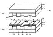
- FIG. 1illustrates an exemplary electromechanical memory array 100 in exploded view.
- the arraycontains a layer of nanotube ribbons 101 between an upper structure 102 and a lower structure 103 .
- the lower structure 103includes a plurality of generally parallel electrically conductive traces 104 , disposed between generally parallel and upwardly-protruding supports 105 .
- the traces 104 and supports 105are generally perpendicular to the ribbons 101 .
- the traces and supportsare arranged over a gate oxide layer 109 and silicon substrate 110 .
- the upper structure 102is similar to the lower structure.
- the upper structure 102includes a plurality of generally parallel electrically conductive traces 114 , disposed between generally parallel and downwardly-protruding supports 115 .
- the traces 114 and supports 115are generally perpendicular to the ribbons 101 .
- the traces and supportsare arranged over a gate oxide layer 119 and silicon substrate 120 .
- the electromechanically responsive elements 101are nanotube ribbons. However, other materials, including nanotubes, may be used. Under certain preferred embodiments, a nanotube ribbon 101 has a width of about 180 nm and is pinned to insulating supports 102 (more below).
- the traces 104 , 114may be made of any suitable electrically conductive material and may be arranged in any of a variety of suitable geometries. Certain preferred embodiments utilize n-doped silicon to form such traces, preferably no wider than the nanotube belt 101 , e.g., about 180 nm.
- the supports 102 and 112may be made of a variety of materials and geometries, but certain preferred embodiments utilize insulating material, such as spin-on-glass (SOG).
- SOGspin-on-glass
- the preferred thickness (height)must equal or exceed the height of the electrodes preferably from 100 nm to 1 micron.
- the ribbons 101are held between the contacting supports by friction.
- the ribbonmay be held by other means, such as by anchoring the ribbons to the supports using any of a variety of techniques.
- the nanotube ribbons 101are also pinned to the upper surfaces of lower supports 102 by the upper supports being deposited on top of the lower supports.
- Evaporated or spin-coated materialsuch as metals, semiconductors or insulators—especially silicon, titanium, silicon oxide or polyimide—may be used to increase the pinning strength.
- the friction interactioncan be increased through the use of chemical interactions, including covalent bonding through the use of carbon compounds such as pyrenes or other chemically reactive species. See R. J.
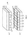
- Each instance where a ribbon crosses corresponding, oppositely-disposed tracesdefines a memory or logic cell.
- the actual number of such cellsis immaterial to understanding the invention, but the technology may support devices having information storage capacities at least on the order of modem nonvolatile circuit devices.
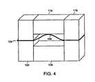
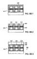
- FIGS. 2-4are cross-sectional diagrams of a cell and illustrate various states of the device.
- a given cellmay be used to have three states assigned as “on” and “off” states.
- State 106may be assigned as an “off,” and states 107 and 108 may be assigned as “on” states 107 and 108 .
- the ribbon 101When the device is in state 106 , the ribbon 101 is separated from both electrically conductive traces 104 and 114 by a distance 110 . (The figure may suggest that the distances 110 between the ribbon and a corresponding trace is equal, but they need not be.)
- This statemay be electrically detected in any of a variety of ways described in the foregoing references incorporated by reference.
- the cellWhen the cell is in state 107 , shown in FIG. 3 , the ribbon is deflected toward trace 104 .
- the cellWhen the cell is in state 108 , shown in FIG. 4 , the ribbon is deflected toward trace 114 .
- an “off” statecorresponds to the ribbon-trace junction being an open circuit, which may be sensed as such on either the ribbon 101 or trace 104 when addressed.
- the ribbon-trace junctionis an electrically conducting, rectifying junction (e.g., Schottky or PN), which may be sensed as such on either the ribbon 101 or trace 104 when addressed.
- the relative separation 110 from the top of an insulating support 102 to the deflected position where the belt 101 attaches to electrode 104 or 114should be approximately 5-50 nm.
- the magnitude of the separation 110is designed to be compatible with electromechanical switching capabilities of the memory device.
- the 5-50 nm separationis preferred for certain embodiments utilizing ribbons 101 made from carbon nanotubes, and reflects the specific interplay between strain energy and adhesion energy for the deflected nanotubes. Other separations may be preferable for other materials.
- Switching between these statesis accomplished by the application of specific voltages across the nanotube belt or wire 101 and one or more of its associated conductive traces 104 , 114 . Switching forces are based on the interplay of electrostatic attraction and repulsion between the nanotube ribbon and the electrodes.
- the differences between resistances in the “off” and “on” statesprovides a means to read which state a junction is in.
- a “readout current”is applied to the nanotube belt or electrode and the voltage across the junction is determined with a “sense amplifier” on the traces. Reads are non-destructive, meaning that the cell retains its state, and no write-back operations are needed as is required with semiconductor DRAMs.
- the three-trace junctions of preferred embodimentsbring their own advantages. By allowing for use of tristable memory cells, more information may be stored or represented by a given cell. Moreover, even if only one of the “on” states were used, three-trace junctions may increase switching speeds from the ability to use both conductive traces in concert to apply forces to move an electromechanically responsive trace 101 . Furthermore, advantages in increased reliability and defect tolerance can come from the redundancy permitted, by the presence of two conductive traces in each cell. Each of the two conductive traces may be separately used to apply forces to move an electromechanically responsive trace, and each of the two conductive traces may serve as the “contact” for one of two alternative “on” states.
- the failure of one conductive tracemay not be fatal to junction performance.
- the ribbons 101by disposing the ribbons 101 between upper and lower structures 102 , 103 , the ribbons are effectively sealed and protected. Among other things this facilitates packaging and distribution, and it allows the nanotube-technology arrays to be more easily incorporated into other circuit and systems such as hybrid circuits.
- the lateral nature of the electrical architecturecan also facilitate the production of stackable memory layers and the simplification of various interconnects.
- FIGS. 5A-Dillustrates a method of making certain embodiments of NTRCM devices 100 .
- a first intermediate structure 500is created or provided as explained in the incorporated patent applications, cited above.
- the structure 500includes a silicon substrate 502 having a gate dielectric layer 504 (such as silicon dioxide) and an insulating support layer 506 (such as spin-on-glass (SOG)) that contains a plurality of supports 508 .
- the supports 508are formed by rows of patterned insulating material, though many other arrangements are possible, such as a plurality of columns.
- Conductive traces 510extend between supports 508 . These conductive electrodes can be fabricated from a single material such as n-doped silicon or from a combination of material layers including metal and silicon layers. Acceptable materials for the conductive electrodes include copper, titanium, tungsten, and platinum, or other metals or semiconductors, such as silicon, compatible with standard fabrication lines. In this instance, the traces 510 are shown as essentially contacting the supports 508 , but other arrangements are possible, as are other geometries, such as ones characterized by nonrectangular transverse cross-sections (e.g., triangular or trapezoidal).
- Sacrificial layers 518are disposed above the conductive traces 510 so as to define one planar surface 520 with the upper surface of the supports 508 .
- This planar surfacefacilitates growth of a non-woven fabric of single-walled carbon nanotubes (SWNTs) which is primarily one nanotube thick.
- SWNTssingle-walled carbon nanotubes
- a nanotube filmis first grown on surface 520 and then patterned, e.g., by photolithography and etching, to define a layer of ribbons 522 (see also 101 in FIG. 1 ).
- the ribbons of non-woven nanotube fabriclie on the planar surface 520 and cross (for example, perpendicularly) the underlying traces 510 .
- the resulting intermediate structure 524is the lower structure 102 referred to above, with the exception that structure 524 includes the sacrificial layer 518 .
- the lower intermediate structure 524may be formed in many ways. Several such ways are described in the incorporated patent applications, cited above. In addition, various ways are implicitly suggested through the description below of different ways of constructing analogous structures sitting on top of the lower array.
- An upper intermediate structure 526may be formed separately, and it may be placed on top of the patterned carbon nanotube film layer 522 to yield intermediate structure 540 .
- the upper intermediate structure 526includes an insulating support layer 528 (e.g., SOG) that contains a plurality of supports 530 .
- the supports 530consist of rows of patterned insulating material, but, as with the lower structure, many arrangements are possible, such as ones containing a plurality of columns.
- the insulating supportsmay be made from a variety of materials.
- Conductive traces 532extend between supports 530 .
- the conductive traces 532are shown as essentially contacting the supports 530 , but other arrangements and geometries are possible, as described for the conductive traces 510 in intermediate 500 .
- a gate dielectric layer 536 and a conductive ground layer 538are deposited on top of the supports 530 and traces 532 .
- the lower and upper sacrificial layers 518 and 534have to be removed from intermediate structure 540 , as by using wet or dry chemical etchants including acids or bases.
- the various growth, patterning, and etching operationsmay be performed using conventional techniques, such as lithographic patterning.
- these techniquescan lead to feature sizes (e.g., the width of ribbon 101 ) of about 180 nm to as low as 130 nm, but the physical characteristics of the components are amenable to even smaller feature sizes that may be accessible to future manufacturing processes.
- a second pointis that, because the nanotube ribbons are in place before construction of the upper array begins, there is some more flexibility in the choice of materials for the upper array.
- the choice of materials for the lower electrodesis limited to those substances that will survive the high temperature of the nanotube growth process, the choice of materials for the upper electrodes is not so constrained.
- interconnect fabricationcan be applied using standard metallization and CMOS logic or using nanoelectromechanical addressing as previously explained in the incorporated patent applications, cited above. Such addressing can also be done utilizing a tristable nanoelectromechanical addressing logic scheme.
- FIGS. 6 A 1 through 8 B 3Three possible methods for generating the upper intermediate structure 526 are described in connection with FIGS. 6 A 1 through 8 B 3 .
- FIGS. 6 A 1 through 6 B 3show one approach for producing a three-trace structure 542 .
- a lower intermediate structure 524is provided or constructed using the techniques identified above.
- a sacrificial layer 602(about 10-20 nm high) and an n-doped silicon layer 604 are then added using a CVD process, sputtering, electroplating, or a different deposition process.
- a photoresist layermay be spin-coated on layer 604 and subsequently exposed and developed to create cavities which lie directly over the underlying supports 508 .
- Reactive ion etchingor the like may then be used to etch the electrode and sacrificial layers 604 and 602 to form cavities 608 and to define upper-layer electrodes 610 that are positioned directly above the underlying electrodes 510 .
- the cavities 608are then filled and covered with a planar layer 609 of insulating material such as spin-on-glass (SOG) or polyimide.
- the insulating layer 609is backetched with RIE or a plasma to the same height as the electrodes 610 so as to form a planar surface 616 .
- a gate dielectric layer 620is provided above the surface 616 to separate the electrodes 610 from the upper electrical ground layer 622 . This layer 622 serves the additional purpose of providing a hermetic seal covering the entire memory structure.
- the resulting intermediate structure 540is then processed so that the lower and upper sacrificial layers 518 and 534 , respectively, are removed to result in structure 542 , as discussed above in connection with FIGS. 5A-D .
- FIGS. 7 A 1 through 7 B 3show another approach for producing a three trace structure 542 .
- a lower intermediate structure 524like that described in connection with FIGS. 5A-D is provided or constructed.
- a sacrificial layer 702(about 10-20 nm high) can be selectively grown directly above the underlying sacrificial layer 518 , e.g., by using a selective CVD process involving self-complementary materials such as titanium, to produce intermediate structure 700 .
- the resulting cavities 704are filled and covered with a planar layer 708 of an insulating material such as spin-on-glass (SOG) or polyimide.
- SOGspin-on-glass
- the insulating layer 708is backetched with RIE or a plasma to a height 710 equal to the intended total height of the upper sacrificial layer 702 and the upper conductive electrodes 724 .
- a photoresist layermay be spin-coated on layer 708 and subsequently exposed and lithographically developed to create cavities which lie directly over the underlying electrodes 510 .
- RIEreactive ion etching
- the cavities 714are filled and covered with a planar layer consisting of n-doped silicon or other suitable electrode-forming materials, and this layer is backetched with RIE or a plasma to the same height 710 as the remaining portions of the support layer 722 , the result being intermediate 718 .
- the top surfaces of the upper electrodes 724 and the supports 722form a planar surface 726 .
- a gate dielectric layer 730is deposited on top of intermediate structure 718 to separate the upper electrodes 724 from the upper electrical ground conductive layer 732 (e.g., silicon), which is added on top of the gate dielectric layer. This results in structure 540 like those described above.
- Layer 732serves the additional purpose of providing a hermetic seal covering the entire memory structure.
- the resulting intermediate structure 540is then processed so that the lower and upper sacrificial layers 518 and 534 , respectively, are removed to result in structure 542 , as discussed above in connection with FIGS. 5A-D .
- FIGS. 8 A 1 through 8 B 3show another approach for producing a three trace structure 542 .
- Intermediate structure 700(as explained above) is provided or created.
- the cavities 704are filled with n-doped silicon or other suitable electrode-forming materials to form a planar layer 804 .
- the electrode layer 804is backetched with RIE or a plasma to approximately the same height 710 as previously described.
- a photoresist layermay be spin-coated on layer 804 and subsequently exposed and lithographically developed to begin the creation of cavities 808 which lie directly over the underlying supports 508 .
- RIEreactive ion etching
- the cavities 808 of intermediate 806are then filled and covered with a planar insulating layer, consisting, for example, of SOG or polyimide.
- the insulating layeris backetched with RIE or a plasma to form the supports 722 with a height 710 equal to the total height of the upper sacrificial layer 702 and the upper silicon electrodes 724 .
- the resultis intermediate structure 718 , with a flat surface 726 as previously described.
- Substrate 718is converted into substrate 728 by adding gate dielectric and upper electrical ground layers as described above.
- the resulting intermediate structure 540is then processed so that the lower and upper sacrificial layers 518 and 534 , respectively, are removed to result in structure 542 , as discussed above in connection with FIGS. 5A-D .
- the upper electrodesare not located directly over the lower electrodes but, instead, are shifted (e.g., displaced by half their width) relative to the lower electrodes.
- This approachfacilitates the use of certain techniques for removing sacrificial layers.
- FIGS. 9A-Dillustrates a method of making these “shifted” embodiments of NTRCM devices.
- a first intermediate structure 500as described above, is created or provided. Structure 500 is then converted, as described above, to intermediate 524 featuring patterned nanotube ribbons 522 on top of intermediate 500 .
- Upper insulating supports 902are deposited onto the lower supports 508 , and upper sacrificial layers 904 having the same height as the upper supports 902 are deposited on top of ribbons 522 but in alignment with the lower sacrificial layers 518 , so as to create a flat surface 906 .
- the height of the upper sacrificial layers 904 and upper supports 902is approximately the same as the height of the lower sacrificial layer 518 , e.g., 10-20 nm on average.
- the upper supports 902 and upper sacrificial layers 904may be made of the same materials as the corresponding lower layers but are not limited to these materials.
- Conductive traces 908 of n-type silicon electrodes, or some other suitable material or material combination,are provided on top of the flat surface 906 so that they run parallel to the lower conductive traces 510 and so that at least a portion of the traces 908 (but not their entirety) are aligned with the traces 510 .
- the completed upper array 910 of the resulting intermediate 900includes upper supports 902 , upper sacrificial layers 904 , and upper electrodes 908 .
- the upper conductive traces 908 in intermediate 900are not directly located above the lower electrode traces 510 , but are shifted by a certain amount (e.g., by half their width) relative to the lower traces 510 .
- the lower sacrificial layer 518 and upper sacrificial layer 904are removed using wet or dry chemical etchants including acids or bases.
- the upper traces 908are shown as having rectangular cross-sections and widths similar to those of the lower supports 508 and lower electrodes 510 , but neither the shapes nor the widths of the upper traces 908 is limited to these parameters. Narrower or wider traces of different cross-sections, e.g., trapezoidal or triangular, can be envisioned.
- the choice of material for the lower array 524is somewhat limited so that the materials are compatible with the growth conditions for the carbon nanotubes or nanotube fabrics (e.g., relatively high temperature)
- the upper array 910is fabricated after nanotube growth so that a wider variety of materials can be used for the upper supports 902 , upper sacrificial layers 904 , and upper electrodes 908 .
- materials that are only stable up to relatively low temperaturessuch as polyimides, other polymers or low melting point metals (e.g. aluminum), can be used for the upper array 910 .
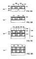
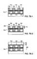
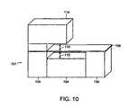
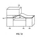
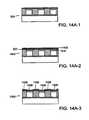
- FIGS. 10-12are cross-sectional diagrams of a cell having a shifted upper electrode and illustrate various states of the device.
- the statesmay be assigned with some meaning, such as “on” and “off” states, or assigned to non-binary encoding.
- FIG. 10shows a junction that may be assigned as an “off” state
- FIGS. 11 and 12show junctions in different “on” states.
- the description of these statesis analogous to that of FIGS. 2-4 and thus will not be repeated.
- Like reference numerals to those of FIGS. 2-4have been used to show corresponding features of these embodiments and states.
- FIGS. 13 A 1 through 13 B 3show one approach for producing a three-trace structure 912 .
- a lower intermediate structure 524is provided or constructed using the techniques identified above.
- a support layer 1302 of about the same height as the lower sacrificial layer 518is deposited to generate intermediate structure 1300 .
- the layer 1302is then patterned by photolithography and etching techniques, such as RIE, to create the supports 902 and to define cavities 1306 of intermediate structure 1304 .
- the cavities 1306are filled with a planar sacrificial layer which is then backetched by RIE or some other etching technique until the sacrificial layer 904 has the same height as the upper supports 902 and a planar surface 906 is formed.
- the intermediate structure 1310 so formedthen has a layer of electrode material, such as n-type silicon, deposited on top of surface 906 , which is then patterned by photolithography and etching techniques, such as RIE, to define conductive electrode traces 908 and to form intermediate structure 900 .
- the upper and lower sacrificial layers 904 and 518are then removed, as explained in conjunction with FIGS. 9A-D , to generate the freely suspended, tristable nanotube junctions 914 of the target structure 912 .
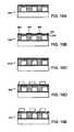
- FIGS. 14 A 1 through 14 B 3show another approach for producing a three-trace structure 912 .
- Intermediate structure 524is provided or created and then transformed into intermediate 1400 by evaporation onto its surface of an upper sacrificial layer 1402 of about the same height as the lower sacrificial layer 518 .
- This sacrificial layeris then patterned by lithography and etching to form sacrificial layer lines 1406 separated by cavities 1408 of intermediate 1404 .
- the cavities 1408are then filled by a flat layer of support material which is backetched to the same height as the sacrificial layer lines 904 to form a flat surface 906 and to form intermediate structure 1310 .
- Intermediate 1310is converted into intermediate 900 as explained in conjunction with FIGS. 13 B 1 - 13 B 3 .
- the upper and lower sacrificial layers 904 and 518are removed to form the target structure 912 containing freely suspended, tristable nanotube junctions 914 .
- FIGS. 15A-Dshows another approach for producing a three-trace structure 912 .
- support layers 902(about 10-20 nm high) are selectively grown on top of the lower structure 524 directly above the lower supports 508 , e.g., by using a selective CVD process involving self-complementary materials such as titanium or silicon dioxide.
- the resulting intermediate 1304is then converted successively into intermediate 1310 , intermediate 900 , and finally the target structure 912 , as described above in conjunction with FIGS. 13 B 1 - 13 B 3 .
- FIGS. 16A-Eshows another approach for producing a three-trace structure 912 .
- Sacrificial layers 904are selectively deposited on the lower array 524 to form intermediate 1404 .
- Intermediate 1404is then converted via intermediates 1310 and 900 into the target structure 912 , as described above in conjunction with FIGS. 14 B 1 - 14 B 3 .
- FIGS. 17A-14Eshows another approach for producing a three-trace structure 912 .
- Intermediate 524is created or provided.
- a sacrificial layer 1402made of the same material as the lower sacrificial layer 518 , and an electrode layer 1702 are deposited to form structure 1700 .
- the electrode layer 1702is then patterned by lithography and RIE to form electrode lines 908 .
- the exposed part of the upper and lower sacrificial layersare removed by RIE to form intermediate 1706 .
- the remaining sacrificial material 1708is located only underneath the electrode lines 908 .
- the now freely suspended nanotube ribbonsform junctions 1710 with a freely suspended length, in the embodiment pictured (in which array elements are assumed to have been made as small as possible), of approximately half the resolution limit of the lithography used for patterning.
- the part 1712 of the sacrificial material remaining directly above the lower electrodes 510is removed. This can be accomplished by utilizing the faster differential solubility of this sacrificial material 1712 compared to the sacrificial material 1714 remaining directly above the lower insulating supports 508 .
- the sacrificial material 1712 directly above the lower electrodesdissolves faster because it is more accessible to the etchant than the part 1714 of the remaining sacrificial layer directly above the lower supports 508 .
- the target structure 1716 featuring freely suspended, tristable nanotube junctions 914can be fabricated.
- FIGS. 18 A through 18 B 3illustrate yet another approach for producing a three-trace structure 912 .
- Intermediate 1800is produced by evaporating a sacrificial layer 1802 and an electrode material layer 1702 onto intermediate 524 .
- the upper sacrificial layers 1802are made of a material that has different etching characteristics than the lower sacrificial layers 518 .
- the electrode material layer 1702is patterned to form the electrode lines 908 of intermediate 1804 . Subsequently, the exposed region of the sacrificial layer 1802 in between electrodes 908 is removed by RIE to form intermediate 1806 of FIGS. 18 B 1 - 18 B 3 . Then the lower sacrificial layer 518 is removed by etching to form intermediate 1808 . The remaining portions 1810 of the upper sacrificial layers directly above the lower electrodes 510 are removed by utilizing their higher differential solubility compared to the portions 1812 of sacrificial material directly above the lower supports 508 .
- sacrificial material 1810 directly above the lower electrodesis much more easily accessed than sacrificial material 1812 directly above the lower supports, the material directly above the lower electrodes etches faster.
- the freely suspended, tristable junctions 914 of the target structure 1814can be generated.
- metallizationmay be used to add addressing electrodes to an array of tristable junctions such as that pictured in FIG. 1 .
- Other embodimentscould use nanotube technology, whether in individual wire or belt form, to implement addressing of memory cells instead of using metallized electrodes and CMOS addressing logic (not shown).
- Such potential use of nanotube technology to select memory cells for reading or writing operationswould further integrate nanotubes into system design and might add beneficial functionality to higher-level system design. For example, under this approach of using nanotube technology for both memory and addressing, the memory architecture could inherently store the last memory address as well as memory contents in a nonvolatile manner.
- Another set of embodimentswould use different materials in place of the nanotube ribbons described above.
- individual nanotubescould be used instead of ribbons, albeit with the disadvantages relative to ribbons discussed above.
- other materials with electronic and mechanical properties suitable for electromechanical switchingcould be envisioned. These materials would have properties similar to carbon nanotubes but with different and likely reduced tensile strength. For a material to qualify, its tensile strain and adhesion energies would need to fall within a range that allowed for bistability or tristability, and that ensured that required electromechanical switching properties exist within acceptable tolerances.
- Additional electrodesconsisting of n-doped silicon on top of some metal or semiconductor conductive traces.
- the additional electrodeswould provide rectifying junctions in the ON state so that no multiple current pathways exist.
- Embodimentscould also feature any of various other widely accepted and used methods to prevent the occurrence of electrical crosstalk (i.e., multiple current pathways) in crossbar arrays.
- Tunnel barrierscould be added on top of the static, lithographically fabricated electrodes to prevent the formation of ohmic ON states. In such embodiments, no leakage currents would occur at zero bias voltage, and a small bias voltage would have to be applied for any significant number of charge carriers to overcome the barrier and tunnel between crossing traces.
- Additional embodimentscould make use of methods to increase adhesion energies through the use of ionic, covalent or other forces to alter the interactions between the electromechanical switching elements and the electrode surfaces. Such methods can be used to extend the range of bistability and tristability within the junctions.
- certain embodimentsused a shifted upper trace to define an opening to the sacrificial layers to facilitate the removal of the sacrificial layers.
- Other approachesmay be used to define such openings, for example, by shaping the upper trace appropriately to define such an opening.
Landscapes
- Engineering & Computer Science (AREA)
- Chemical & Material Sciences (AREA)
- Nanotechnology (AREA)
- Physics & Mathematics (AREA)
- Mathematical Physics (AREA)
- Theoretical Computer Science (AREA)
- Crystallography & Structural Chemistry (AREA)
- Computer Hardware Design (AREA)
- Semiconductor Memories (AREA)
- Carbon And Carbon Compounds (AREA)
- Tests Of Electronic Circuits (AREA)
Abstract
Description
- U.S. application Ser. No. 09/915,093, entitled “Electromechanical Memory Array Using Nanotube Ribbons and Method for Making Same,” filed Jul. 25, 2001.
- U.S. application Ser. No. 09/915,173 entitled “Electromechanical Memory Having Cell Selection Circuitry Constructed with Nanotube Technology,” filed Jul. 25, 2001.
- U.S. application Ser. No. 09/915,095 entitled “Hybrid Circuit Having Nanotube Electromechanical Memory,” filed Jul. 25, 2001.
Claims (45)
Priority Applications (20)
| Application Number | Priority Date | Filing Date | Title |
|---|---|---|---|
| US10/033,323US6911682B2 (en) | 2001-12-28 | 2001-12-28 | Electromechanical three-trace junction devices |
| CA002471378ACA2471378A1 (en) | 2001-12-28 | 2002-12-19 | Electromechanical three-trace junction devices |
| JP2003558875AJP4643145B2 (en) | 2001-12-28 | 2002-12-19 | Electromechanical 3-trace junction device |
| EP09163561AEP2108493A1 (en) | 2001-12-28 | 2002-12-19 | Electromechanical three-trace junction devices |
| PCT/US2002/040852WO2003058652A2 (en) | 2001-12-28 | 2002-12-19 | Electromechanical three-trace junction devices |
| DE60233073TDE60233073D1 (en) | 2001-12-28 | 2002-12-19 | ELECTROMECHANICAL THREE TRACE JUNCTION ELEMENTS |
| EP02802582AEP1459334B1 (en) | 2001-12-28 | 2002-12-19 | Electromechanical three-trace junction devices |
| AU2002364966AAU2002364966A1 (en) | 2001-12-28 | 2002-12-19 | Electromechanical three-trace junction devices |
| TW091137563ATWI303421B (en) | 2001-12-28 | 2002-12-27 | Electromechanical three-trace junction devices |
| TW092101535ATWI307330B (en) | 2001-07-25 | 2003-01-24 | Methods of making non-woven fabric of carbon nanotubes and article |
| TW092101536ATWI313669B (en) | 2001-07-25 | 2003-01-24 | Conductive articles, combined articles, conductive traces and non-woven fabrics made by carbon nanotube |
| US10/776,059US7259410B2 (en) | 2001-07-25 | 2004-02-11 | Devices having horizontally-disposed nanofabric articles and methods of making the same |
| US10/776,572US6924538B2 (en) | 2001-07-25 | 2004-02-11 | Devices having vertically-disposed nanofabric articles and methods of making the same |
| US10/802,900US7176505B2 (en) | 2001-12-28 | 2004-03-17 | Electromechanical three-trace junction devices |
| US11/158,217US7112464B2 (en) | 2001-07-25 | 2005-06-21 | Devices having vertically-disposed nanofabric articles and methods of making the same |
| US11/158,544US7274078B2 (en) | 2001-07-25 | 2005-06-22 | Devices having vertically-disposed nanofabric articles and methods of making the same |
| US11/193,795US7304357B2 (en) | 2001-07-25 | 2005-07-29 | Devices having horizontally-disposed nanofabric articles and methods of making the same |
| US11/454,216US7521736B2 (en) | 2001-12-28 | 2006-06-15 | Electromechanical three-trace junction devices |
| US11/526,364US7719067B2 (en) | 2001-07-25 | 2006-09-25 | Devices having vertically-disposed nanofabric articles and methods of making the same |
| US11/999,228US7619291B2 (en) | 2001-07-25 | 2007-12-04 | Devices having horizontally-disposed nanofabric articles and methods of making the same |
Applications Claiming Priority (1)
| Application Number | Priority Date | Filing Date | Title |
|---|---|---|---|
| US10/033,323US6911682B2 (en) | 2001-12-28 | 2001-12-28 | Electromechanical three-trace junction devices |
Related Parent Applications (1)
| Application Number | Title | Priority Date | Filing Date |
|---|---|---|---|
| US09/915,093Continuation-In-PartUS6919592B2 (en) | 2001-07-25 | 2001-07-25 | Electromechanical memory array using nanotube ribbons and method for making same |
Related Child Applications (11)
| Application Number | Title | Priority Date | Filing Date |
|---|---|---|---|
| US09/915,093Continuation-In-PartUS6919592B2 (en) | 2001-07-25 | 2001-07-25 | Electromechanical memory array using nanotube ribbons and method for making same |
| US09/915,173Continuation-In-PartUS6643165B2 (en) | 2001-07-25 | 2001-07-25 | Electromechanical memory having cell selection circuitry constructed with nanotube technology |
| US10/128,118Continuation-In-PartUS6706402B2 (en) | 2001-07-25 | 2002-04-23 | Nanotube films and articles |
| US10128118Continuation-In-Part | 2003-01-13 | ||
| US10/341,005Continuation-In-PartUS7566478B2 (en) | 2001-07-25 | 2003-01-13 | Methods of making carbon nanotube films, layers, fabrics, ribbons, elements and articles |
| US10/776,059Continuation-In-PartUS7259410B2 (en) | 2001-07-25 | 2004-02-11 | Devices having horizontally-disposed nanofabric articles and methods of making the same |
| US10/776,572Continuation-In-PartUS6924538B2 (en) | 2001-07-25 | 2004-02-11 | Devices having vertically-disposed nanofabric articles and methods of making the same |
| US10/802,900Continuation-In-PartUS7176505B2 (en) | 2001-12-28 | 2004-03-17 | Electromechanical three-trace junction devices |
| US11/158,217Continuation-In-PartUS7112464B2 (en) | 2001-07-25 | 2005-06-21 | Devices having vertically-disposed nanofabric articles and methods of making the same |
| US11/158,544Continuation-In-PartUS7274078B2 (en) | 2001-07-25 | 2005-06-22 | Devices having vertically-disposed nanofabric articles and methods of making the same |
| US11/193,795Continuation-In-PartUS7304357B2 (en) | 2001-07-25 | 2005-07-29 | Devices having horizontally-disposed nanofabric articles and methods of making the same |
Publications (2)
| Publication Number | Publication Date |
|---|---|
| US20030124325A1 US20030124325A1 (en) | 2003-07-03 |
| US6911682B2true US6911682B2 (en) | 2005-06-28 |
Family
ID=21869744
Family Applications (1)
| Application Number | Title | Priority Date | Filing Date |
|---|---|---|---|
| US10/033,323Expired - LifetimeUS6911682B2 (en) | 2001-07-25 | 2001-12-28 | Electromechanical three-trace junction devices |
Country Status (8)
| Country | Link |
|---|---|
| US (1) | US6911682B2 (en) |
| EP (2) | EP1459334B1 (en) |
| JP (1) | JP4643145B2 (en) |
| AU (1) | AU2002364966A1 (en) |
| CA (1) | CA2471378A1 (en) |
| DE (1) | DE60233073D1 (en) |
| TW (3) | TWI303421B (en) |
| WO (1) | WO2003058652A2 (en) |
Cited By (70)
| Publication number | Priority date | Publication date | Assignee | Title |
|---|---|---|---|---|
| US20030151257A1 (en)* | 2001-06-20 | 2003-08-14 | Ambient Systems, Inc. | Energy conversion systems using nanometer scale assemblies and methods for using same |
| US20040239210A1 (en)* | 2003-06-02 | 2004-12-02 | Pinkerton Joseph F. | Electrical assemblies using molecular-scale electrically conductive and mechanically flexible beams and methods for application of same |
| US20040240252A1 (en)* | 2003-06-02 | 2004-12-02 | Pinkerton Joseph F. | Nanoelectromechanical memory cells and data storage devices |
| US20040239119A1 (en)* | 2003-06-02 | 2004-12-02 | Pinkerton Joseph F. | Energy conversion systems utilizing parallel array of automatic switches and generators |
| US20040238907A1 (en)* | 2003-06-02 | 2004-12-02 | Pinkerton Joseph F. | Nanoelectromechanical transistors and switch systems |
| US20050101112A1 (en)* | 2001-07-25 | 2005-05-12 | Nantero, Inc. | Methods of nanotubes films and articles |
| US20060172126A1 (en)* | 2005-01-28 | 2006-08-03 | Long David P | Magnetically directed self-assembly of molecular electronic junctions |
| US20060183278A1 (en)* | 2005-01-14 | 2006-08-17 | Nantero, Inc. | Field effect device having a channel of nanofabric and methods of making same |
| US20060193093A1 (en)* | 2004-11-02 | 2006-08-31 | Nantero, Inc. | Nanotube ESD protective devices and corresponding nonvolatile and volatile nanotube switches |
| US20060231865A1 (en)* | 2001-12-28 | 2006-10-19 | Nantero, Inc. | Electromechanical three-trace junction devices |
| US20060237857A1 (en)* | 2005-01-14 | 2006-10-26 | Nantero, Inc. | Hybrid carbon nanotube FET(CNFET)-FET static RAM (SRAM) and method of making same |
| US20060250856A1 (en)* | 2005-05-09 | 2006-11-09 | Nantero, Inc. | Memory arrays using nanotube articles with reprogrammable resistance |
| US20060250843A1 (en)* | 2005-05-09 | 2006-11-09 | Nantero, Inc. | Non-volatile-shadow latch using a nanotube switch |
| US20060258122A1 (en)* | 2005-05-12 | 2006-11-16 | Whitefield Bruce J | Nanotube fuse structure |
| WO2006137876A2 (en) | 2004-09-22 | 2006-12-28 | Nantero, Inc. | Random access memory including nanotube switching elements |
| US20070048160A1 (en)* | 2005-07-19 | 2007-03-01 | Pinkerton Joseph F | Heat activated nanometer-scale pump |
| US20070045119A1 (en)* | 2005-09-01 | 2007-03-01 | Micron Technology, Inc. | Methods and apparatus for sorting and/or depositing nanotubes |
| WO2007053180A1 (en) | 2005-05-09 | 2007-05-10 | Nantero, Inc. | Two-terminal nanotube devices and systems and methods of making same |
| US7274078B2 (en) | 2001-07-25 | 2007-09-25 | Nantero, Inc. | Devices having vertically-disposed nanofabric articles and methods of making the same |
| US20070237959A1 (en)* | 2005-09-06 | 2007-10-11 | Lemaire Charles A | Apparatus and method for growing fullerene nanotube forests, and forming nanotube films, threads and composite structures therefrom |
| US20070236325A1 (en)* | 2004-09-21 | 2007-10-11 | Nantero, Inc. | Resistive elements using carbon nanotubes |
| US20070262687A1 (en)* | 2006-01-03 | 2007-11-15 | Nano-Proprietary, Inc. | Curing binder material for carbon nanotube electron emission cathodes |
| US7304357B2 (en) | 2001-07-25 | 2007-12-04 | Nantero, Inc. | Devices having horizontally-disposed nanofabric articles and methods of making the same |
| WO2008021900A2 (en) | 2006-08-08 | 2008-02-21 | Nantero, Inc. | Nonvolatile nanotube diodes and nonvolatile nanotube blocks and systems using same and methods of making same |
| US7335395B2 (en) | 2002-04-23 | 2008-02-26 | Nantero, Inc. | Methods of using pre-formed nanotubes to make carbon nanotube films, layers, fabrics, ribbons, elements and articles |
| US7342818B2 (en) | 2001-07-25 | 2008-03-11 | Nantero, Inc. | Hybrid circuit having nanotube electromechanical memory |
| US20080157126A1 (en)* | 2005-05-09 | 2008-07-03 | Nantero, Inc. | Nonvolatile nanotube diodes and nonvolatile nanotube blocks and systems using same and methods of making same |
| US20080169488A1 (en)* | 2001-07-25 | 2008-07-17 | Nantero, Inc. | Device selection circuitry constructed with nanotube technology |
| US20080170429A1 (en)* | 2005-05-09 | 2008-07-17 | Nantero, Inc. | Nonvolatile nanotube diodes and nonvolatile nanotube blocks and systems using same and methods of making same |
| US20080233744A1 (en)* | 2005-09-19 | 2008-09-25 | California Institute Of Technology | Carbon nanotube switches for memory, rf communications and sensing applications, and methods of making the same |
| US20080251865A1 (en)* | 2007-04-03 | 2008-10-16 | Pinkerton Joseph F | Nanoelectromechanical systems and methods for making the same |
| US20090014803A1 (en)* | 2007-07-10 | 2009-01-15 | International Business Machines Corporation | Nanoelectromechanical transistors and methods of forming same |
| US20090017572A1 (en)* | 2007-07-11 | 2009-01-15 | International Business Machines Corporation | Nanoelectromechanical transistors and methods of forming same |
| US20090052246A1 (en)* | 2005-05-09 | 2009-02-26 | Nantero, Inc. | Non-volatile shadow latch using a nanotube switch |
| US7501636B1 (en) | 2007-09-20 | 2009-03-10 | The United States Of America As Represented By The Administrator Of The National Aeronautics And Space Administration | Nanotunneling junction-based hyperspectal polarimetric photodetector and detection method |
| US20090074607A1 (en)* | 2007-09-18 | 2009-03-19 | Barrick Gold Corporation | Process for recovering gold and silver from refractory ores |
| US20090071295A1 (en)* | 2007-09-17 | 2009-03-19 | Barrick Gold Corporation | Method to improve recovery of gold from double refractory gold ores |
| US7518283B2 (en) | 2004-07-19 | 2009-04-14 | Cjp Ip Holdings Ltd. | Nanometer-scale electrostatic and electromagnetic motors and generators |
| US20090140167A1 (en)* | 2005-09-06 | 2009-06-04 | Natero, Inc. | Nanotube fabric-based sensor systems and methods of making same |
| US20090175068A1 (en)* | 2008-01-07 | 2009-07-09 | International Business Machines Corporation | Sram device, and sram device design structure, with adaptable access transistors |
| US7560136B2 (en) | 2003-01-13 | 2009-07-14 | Nantero, Inc. | Methods of using thin metal layers to make carbon nanotube films, layers, fabrics, ribbons, elements and articles |
| US20090184389A1 (en)* | 2005-05-09 | 2009-07-23 | Bertin Claude L | Nonvolatile Nanotube Diodes and Nonvolatile Nanotube Blocks and Systems Using Same and Methods of Making Same |
| US20090194839A1 (en)* | 2005-11-15 | 2009-08-06 | Bertin Claude L | Nonvolatile nanotube diodes and nonvolatile nanotube blocks and systems using same and methods of making same |
| US20090258787A1 (en)* | 2008-03-30 | 2009-10-15 | Hills, Inc. | Superconducting Wires and Cables and Methods for Producing Superconducting Wires and Cables |
| US20090256594A1 (en)* | 2008-04-09 | 2009-10-15 | International Business Machines Corporation | Nanoelectromechanical digital inverter |
| US20090303337A1 (en)* | 2003-07-18 | 2009-12-10 | Katsumi Kaneko | Image pick-up device and synchronization-signal-generating device |
| US20100061143A1 (en)* | 2006-09-22 | 2010-03-11 | Carley L Richard | Assembling and Applying Nano-Electro-Mechanical Systems |
| US20100072042A1 (en)* | 2005-05-09 | 2010-03-25 | Bertin Claude L | Memory elements and cross point switches and arrays of same using nonvolatile nanotube blocks |
| US20100091558A1 (en)* | 2008-10-10 | 2010-04-15 | Macronix International Co., Ltd. | Dielectric-Sandwiched Pillar Memory Device |
| US20100148183A1 (en)* | 2001-07-25 | 2010-06-17 | Ward Jonathan W | Method of Forming a Carbon Nanotube-Based Contact to Semiconductor |
| US20100147657A1 (en)* | 2004-11-02 | 2010-06-17 | Nantero, Inc. | Nanotube esd protective devices and corresponding nonvolatile and volatile nanotube switches |
| US7744793B2 (en) | 2005-09-06 | 2010-06-29 | Lemaire Alexander B | Apparatus and method for growing fullerene nanotube forests, and forming nanotube films, threads and composite structures therefrom |
| US7745810B2 (en) | 2001-07-25 | 2010-06-29 | Nantero, Inc. | Nanotube films and articles |
| US7780918B2 (en) | 2003-05-14 | 2010-08-24 | Nantero, Inc. | Sensor platform using a horizontally oriented nanotube element |
| US7790494B2 (en) | 2007-01-16 | 2010-09-07 | Samsung Electronics Co., Ltd. | Method of fabricating a multi-bit electro-mechanical memory device |
| US20110056812A1 (en)* | 2009-09-08 | 2011-03-10 | Kaul Anupama B | Nano-electro-mechanical switches using three-dimensional sidewall-conductive carbon nanofibers and method for making the same |
| US20110057717A1 (en)* | 2007-06-22 | 2011-03-10 | Nantero, Inc. | Two-terminal nanotube devices including a nanotube bridge and methods of making same |
| US20110212535A1 (en)* | 2010-01-13 | 2011-09-01 | Kaul Anupama B | Applications and methods of operating a three-dimensional nano-electro-mechanical resonator and related devices |
| US8110883B2 (en) | 2007-03-12 | 2012-02-07 | Nantero Inc. | Electromagnetic and thermal sensors using carbon nanotubes and methods of making same |
| US8125824B1 (en) | 2010-09-02 | 2012-02-28 | Lockheed Martin Corporation | Nanotube random access memory (NRAM) and transistor integration |
| WO2012078139A1 (en) | 2010-12-07 | 2012-06-14 | Primaxx, Inc. | Process for manufacturing electro-mechanical systems |
| US8253171B1 (en) | 2009-08-27 | 2012-08-28 | Lockheed Martin Corporation | Two terminal nanotube switch, memory array incorporating the same and method of making |
| US8262770B2 (en) | 2007-09-18 | 2012-09-11 | Barrick Gold Corporation | Process for controlling acid in sulfide pressure oxidation processes |
| US8350360B1 (en) | 2009-08-28 | 2013-01-08 | Lockheed Martin Corporation | Four-terminal carbon nanotube capacitors |
| US8405189B1 (en) | 2010-02-08 | 2013-03-26 | Lockheed Martin Corporation | Carbon nanotube (CNT) capacitors and devices integrated with CNT capacitors |
| US8471238B2 (en) | 2004-09-16 | 2013-06-25 | Nantero Inc. | Light emitters using nanotubes and methods of making same |
| US8630091B2 (en) | 2005-09-06 | 2014-01-14 | Nantero Inc. | Carbon nanotubes for the selective transfer of heat from electronics |
| US9196766B1 (en) | 2012-04-25 | 2015-11-24 | Magnolia Optical Technologies, Inc. | Thermal detectors using graphene and oxides of graphene and methods of making the same |
| US9390790B2 (en) | 2005-04-05 | 2016-07-12 | Nantero Inc. | Carbon based nonvolatile cross point memory incorporating carbon based diode select devices and MOSFET select devices for memory and logic applications |
| US9911743B2 (en) | 2005-05-09 | 2018-03-06 | Nantero, Inc. | Nonvolatile nanotube diodes and nonvolatile nanotube blocks and systems using same and methods of making same |
Families Citing this family (46)
| Publication number | Priority date | Publication date | Assignee | Title |
|---|---|---|---|---|
| US6919592B2 (en) | 2001-07-25 | 2005-07-19 | Nantero, Inc. | Electromechanical memory array using nanotube ribbons and method for making same |
| WO2004065671A1 (en) | 2003-01-13 | 2004-08-05 | Nantero, Inc. | Carbon nanotube films, layers, fabrics, ribbons, elements and articles |
| US7858185B2 (en)* | 2003-09-08 | 2010-12-28 | Nantero, Inc. | High purity nanotube fabrics and films |
| CA2515724A1 (en) | 2003-02-12 | 2004-08-26 | Nantero, Inc | Devices having vertically-disposed nanofabric articles and methods of making the same |
| EP1609188A4 (en) | 2003-03-28 | 2007-11-07 | Nantero Inc | Nanotube-on-gate fet structures and applications |
| US7075141B2 (en)* | 2003-03-28 | 2006-07-11 | Nantero, Inc. | Four terminal non-volatile transistor device |
| US6944054B2 (en)* | 2003-03-28 | 2005-09-13 | Nantero, Inc. | NRAM bit selectable two-device nanotube array |
| US7113426B2 (en)* | 2003-03-28 | 2006-09-26 | Nantero, Inc. | Non-volatile RAM cell and array using nanotube switch position for information state |
| US7294877B2 (en)* | 2003-03-28 | 2007-11-13 | Nantero, Inc. | Nanotube-on-gate FET structures and applications |
| US7045421B2 (en)* | 2003-04-22 | 2006-05-16 | Nantero, Inc. | Process for making bit selectable devices having elements made with nanotubes |
| US6995046B2 (en) | 2003-04-22 | 2006-02-07 | Nantero, Inc. | Process for making byte erasable devices having elements made with nanotubes |
| US7301802B2 (en)* | 2003-06-09 | 2007-11-27 | Nantero, Inc. | Circuit arrays having cells with combinations of transistors and nanotube switching elements |
| US7274064B2 (en)* | 2003-06-09 | 2007-09-25 | Nanatero, Inc. | Non-volatile electromechanical field effect devices and circuits using same and methods of forming same |
| US7115960B2 (en)* | 2003-08-13 | 2006-10-03 | Nantero, Inc. | Nanotube-based switching elements |
| EP1665278A4 (en)* | 2003-08-13 | 2007-11-07 | Nantero Inc | NANOTUBE SWITCHING ELEMENTS COMPRISING MULTIPLE CONTROLS AND CIRCUITS PRODUCED FROM THESE ELEMENTS |
| US7289357B2 (en)* | 2003-08-13 | 2007-10-30 | Nantero, Inc. | Isolation structure for deflectable nanotube elements |
| WO2005017967A2 (en)* | 2003-08-13 | 2005-02-24 | Nantero, Inc. | Nanotube device structure and methods of fabrication |
| CN1868002B (en)* | 2003-08-13 | 2011-12-14 | 南泰若股份有限公司 | Nanotube-based switching element with multiple controls and circuits made therefrom |
| US7375369B2 (en) | 2003-09-08 | 2008-05-20 | Nantero, Inc. | Spin-coatable liquid for formation of high purity nanotube films |
| US7416993B2 (en)* | 2003-09-08 | 2008-08-26 | Nantero, Inc. | Patterned nanowire articles on a substrate and methods of making the same |
| US7504051B2 (en)* | 2003-09-08 | 2009-03-17 | Nantero, Inc. | Applicator liquid for use in electronic manufacturing processes |
| US7034332B2 (en)* | 2004-01-27 | 2006-04-25 | Hewlett-Packard Development Company, L.P. | Nanometer-scale memory device utilizing self-aligned rectifying elements and method of making |
| US7528437B2 (en)* | 2004-02-11 | 2009-05-05 | Nantero, Inc. | EEPROMS using carbon nanotubes for cell storage |
| US7658869B2 (en)* | 2004-06-03 | 2010-02-09 | Nantero, Inc. | Applicator liquid containing ethyl lactate for preparation of nanotube films |
| US7556746B2 (en)* | 2004-06-03 | 2009-07-07 | Nantero, Inc. | Method of making an applicator liquid for electronics fabrication process |
| US7709880B2 (en)* | 2004-06-09 | 2010-05-04 | Nantero, Inc. | Field effect devices having a gate controlled via a nanotube switching element |
| US7164744B2 (en)* | 2004-06-18 | 2007-01-16 | Nantero, Inc. | Nanotube-based logic driver circuits |
| US7288970B2 (en)* | 2004-06-18 | 2007-10-30 | Nantero, Inc. | Integrated nanotube and field effect switching device |
| US7330709B2 (en)* | 2004-06-18 | 2008-02-12 | Nantero, Inc. | Receiver circuit using nanotube-based switches and logic |
| US7161403B2 (en) | 2004-06-18 | 2007-01-09 | Nantero, Inc. | Storage elements using nanotube switching elements |
| US7652342B2 (en)* | 2004-06-18 | 2010-01-26 | Nantero, Inc. | Nanotube-based transfer devices and related circuits |
| US7329931B2 (en)* | 2004-06-18 | 2008-02-12 | Nantero, Inc. | Receiver circuit using nanotube-based switches and transistors |
| US7167026B2 (en)* | 2004-06-18 | 2007-01-23 | Nantero, Inc. | Tri-state circuit using nanotube switching elements |
| EP1825038B1 (en) | 2004-12-16 | 2012-09-12 | Nantero, Inc. | Aqueous carbon nanotube applicator liquids and methods for producing applicator liquids thereof |
| JP5054936B2 (en)* | 2005-06-22 | 2012-10-24 | パナソニック株式会社 | Electromechanical memory, electric circuit using the same, and driving method of electromechanical memory |
| JP5019192B2 (en)* | 2005-06-24 | 2012-09-05 | 株式会社東芝 | Semiconductor device |
| KR100723412B1 (en)* | 2005-11-10 | 2007-05-30 | 삼성전자주식회사 | Nonvolatile Memory Devices Using Nanotubes |
| US7385839B2 (en)* | 2005-12-01 | 2008-06-10 | International Business Machines Corporation | Memory devices using carbon nanotube (CNT) technologies |
| JP4843760B2 (en)* | 2005-12-26 | 2011-12-21 | 株式会社発明屋 | Memory element using carbon nanotube |
| DE102006004218B3 (en)* | 2006-01-30 | 2007-08-16 | Infineon Technologies Ag | Electromechanical storage device and method for manufacturing an electromechanical storage device |
| KR100790822B1 (en)* | 2006-08-07 | 2008-01-02 | 삼성전자주식회사 | Nonvolatile Memory Device and Manufacturing Method Thereof |
| US9263126B1 (en) | 2010-09-01 | 2016-02-16 | Nantero Inc. | Method for dynamically accessing and programming resistive change element arrays |
| US8128993B2 (en) | 2009-07-31 | 2012-03-06 | Nantero Inc. | Anisotropic nanotube fabric layers and films and methods of forming same |
| US8574673B2 (en) | 2009-07-31 | 2013-11-05 | Nantero Inc. | Anisotropic nanotube fabric layers and films and methods of forming same |
| CN102452648B (en)* | 2010-10-27 | 2013-09-25 | 北京富纳特创新科技有限公司 | Carbon nanotube film carrying structure and use method thereof |
| CN112814385A (en)* | 2021-02-22 | 2021-05-18 | 齐鲁工业大学 | 3D building printing equipment |
Citations (266)
| Publication number | Priority date | Publication date | Assignee | Title |
|---|---|---|---|---|
| US3448302A (en) | 1966-06-16 | 1969-06-03 | Itt | Operating circuit for phase change memory devices |
| US3740494A (en) | 1970-11-24 | 1973-06-19 | Sescosem Soc Europ Semiconduct | Electromechanical vibration pick-ups and record pick-ups with field effect transistors |
| US3892890A (en) | 1972-05-12 | 1975-07-01 | Hitachi Ltd | Process for forming carbon coatings |
| US3970887A (en)* | 1974-06-19 | 1976-07-20 | Micro-Bit Corporation | Micro-structure field emission electron source |
| US4324814A (en) | 1981-03-19 | 1982-04-13 | Rca Corporation | Method for forming a narrow thin film line |
| US4378629A (en) | 1979-08-10 | 1983-04-05 | Massachusetts Institute Of Technology | Semiconductor embedded layer technology including permeable base transistor, fabrication method |
| US4495511A (en) | 1982-08-23 | 1985-01-22 | The United States Of America As Represented By The Secretary Of The Navy | Permeable base transistor structure |
| US4510016A (en) | 1982-12-09 | 1985-04-09 | Gte Laboratories | Method of fabricating submicron silicon structures such as permeable base transistors |
| US4524431A (en) | 1982-02-01 | 1985-06-18 | Texas Instruments Incorporated | High-speed nonvolatile memory array |
| EP0217023A2 (en) | 1985-10-04 | 1987-04-08 | International Business Machines Corporation | Pipelined instruction execution with fast branch instructions |
| US4673474A (en) | 1984-10-16 | 1987-06-16 | Matsushita Electric Industrial Co., Ltd. | Molecular controlled structure and method of producing the same |
| US4694427A (en) | 1984-09-21 | 1987-09-15 | Kabushiki Kaisha Toshiba | Programmable semiconductor memory device with combined sense amplification and programming capability |
| US4707197A (en) | 1984-08-02 | 1987-11-17 | American Telephone And Telegraph Company, At&T Bell Laboratories | Method of producing a silicide/Si heteroepitaxial structure, and articles produced by the method |
| EP0269255A2 (en) | 1986-11-27 | 1988-06-01 | Moore Business Forms, Inc. | Adhesive slash pockets |
| US4758534A (en) | 1985-11-13 | 1988-07-19 | Bell Communications Research, Inc. | Process for producing porous refractory metal layers embedded in semiconductor devices |
| EP0296716A2 (en) | 1987-06-22 | 1988-12-28 | Energy Conversion Devices, Inc. | Data storage device having a phase change memory medium reversible by direct overwrite and method of direct overwrite |
| US4819212A (en) | 1986-05-31 | 1989-04-04 | Kabushiki Kaisha Toshiba | Nonvolatile semiconductor memory device with readout test circuitry |
| EP0315392A2 (en) | 1987-11-05 | 1989-05-10 | Energy Conversion Devices, Inc. | Data storage device having an encapsulated phase change memory medium and means for suppressing ablation thereof |
| US4845533A (en) | 1986-08-22 | 1989-07-04 | Energy Conversion Devices, Inc. | Thin film electrical devices with amorphous carbon electrodes and method of making same |
| US4853893A (en) | 1987-07-02 | 1989-08-01 | Ramtron Corporation | Data storage device and method of using a ferroelectric capacitance divider |
| US4876667A (en) | 1987-06-22 | 1989-10-24 | Energy Conversion Devices, Inc. | Data storage device having a phase change memory medium reversible by direct overwrite |
| US4888630A (en) | 1988-03-21 | 1989-12-19 | Texas Instruments Incorporated | Floating-gate transistor with a non-linear intergate dielectric |
| US4901121A (en) | 1985-03-29 | 1990-02-13 | American Telephone & Telegraph Co., At&T Bell Labs. | Semiconductor device comprising a perforated metal silicide layer |
| US4903090A (en) | 1984-11-19 | 1990-02-20 | Fujitsu Limited | Semiconductor device |
| US4939556A (en) | 1986-07-10 | 1990-07-03 | Canon Kabushiki Kaisha | Conductor device |
| US4947226A (en) | 1987-12-08 | 1990-08-07 | Hoenywell, Inc. | Bilateral switching device |
| US4979149A (en)* | 1986-09-10 | 1990-12-18 | Lgz Landis & Gyr Zug Ag | Non-volatile memory device including a micro-mechanical storage element |
| US4985871A (en) | 1989-11-13 | 1991-01-15 | Chips And Technologies, Inc. | Memory controller for using reserved dram addresses for expanded memory space |
| US5010037A (en) | 1988-10-14 | 1991-04-23 | California Institute Of Technology | Pinhole-free growth of epitaxial CoSi2 film on Si(111) |
| US5031145A (en) | 1989-03-29 | 1991-07-09 | Hughes Microelectronics Limited | Sense amplifier |
| US5032538A (en) | 1979-08-10 | 1991-07-16 | Massachusetts Institute Of Technology | Semiconductor embedded layer technology utilizing selective epitaxial growth methods |
| EP0441409A3 (en) | 1987-07-29 | 1991-08-28 | Kabushiki Kaisha Toshiba | Nonvolatile semiconductor memory device |
| US5051956A (en) | 1988-03-25 | 1991-09-24 | Hughes Microelectronics Limited | Memory cell having means for maintaining the gate and substrate at the same potential |
| US5057883A (en) | 1989-05-10 | 1991-10-15 | Mitsubishi Denki Kabushiki Kaisha | Permeable base transistor with gate fingers |
| US5089545A (en) | 1989-02-12 | 1992-02-18 | Biotech International, Inc. | Switching and memory elements from polyamino acids and the method of their assembly |
| US5155561A (en) | 1988-01-05 | 1992-10-13 | Massachusetts Institute Of Technology | Permeable base transistor having an electrode configuration for heat dissipation |
| US5161218A (en) | 1989-11-13 | 1992-11-03 | Chips And Technologies, Inc. | Memory controller for using reserved DRAM addresses for EMS |
| US5168070A (en) | 1990-02-07 | 1992-12-01 | Forschungszentrum Julich Gmbh | Electronic component, especially a permeable base transistor |
| US5175597A (en) | 1990-06-15 | 1992-12-29 | Thomson-Csf | Semiconductor component with schottky junction for microwave amplification and fast logic circuits |
| US5184320A (en) | 1988-02-12 | 1993-02-02 | Texas Instruments Incorporated | Cached random access memory device and system |
| US5196396A (en) | 1991-07-16 | 1993-03-23 | The President And Fellows Of Harvard College | Method of making a superconducting fullerene composition by reacting a fullerene with an alloy containing alkali metal |
| US5198994A (en) | 1988-08-31 | 1993-03-30 | Kabushiki Kaisha Toshiba | Ferroelectric memory device |
| US5198390A (en) | 1992-01-16 | 1993-03-30 | Cornell Research Foundation, Inc. | RIE process for fabricating submicron, silicon electromechanical structures |
| US5216631A (en)* | 1990-11-02 | 1993-06-01 | Sliwa Jr John W | Microvibratory memory device |
| US5252835A (en) | 1992-07-17 | 1993-10-12 | President And Trustees Of Harvard College | Machining oxide thin-films with an atomic force microscope: pattern and object formation on the nanometer scale |
| US5290715A (en) | 1991-12-31 | 1994-03-01 | U.S. Philips Corporation | Method of making dielectrically isolated metal base transistors and permeable base transistors |
| EP0613130A1 (en) | 1993-02-26 | 1994-08-31 | Nec Corporation | Carbon material originating from graphite and method of producing same |
| US5346683A (en) | 1993-03-26 | 1994-09-13 | Gas Research Institute | Uncapped and thinned carbon nanotubes and process |
| WO1995002709A3 (en) | 1993-07-15 | 1995-04-06 | Harvard College | EXTENDED NITRIDE MATERIAL COMPRISING β-C3N¿4? |
| US5412785A (en) | 1990-04-09 | 1995-05-02 | Motorola, Inc. | Microprogrammed data processor which includes a microsequencer in which a next microaddress output of a microROM is connected to the or-plane of an entry PLA |
| US5424054A (en) | 1993-05-21 | 1995-06-13 | International Business Machines Corporation | Carbon fibers and method for their production |
| US5426070A (en) | 1993-05-26 | 1995-06-20 | Cornell Research Foundation, Inc. | Microstructures and high temperature isolation process for fabrication thereof |
| EP0665187A1 (en) | 1994-01-28 | 1995-08-02 | Director-General Of The Agency Of Industrial Science And Technology | Method and device for the production of carbon nanotubes |
| US5444421A (en) | 1994-02-10 | 1995-08-22 | Racom Systems, Inc. | Low power consumption oscillator using multiple transconductance amplifiers |
| US5444651A (en) | 1991-10-30 | 1995-08-22 | Sharp Kabushiki Kaisha | Non-volatile memory device |
| US5453970A (en) | 1993-07-13 | 1995-09-26 | Rust; Thomas F. | Molecular memory medium and molecular memory disk drive for storing information using a tunnelling probe |
| US5456986A (en) | 1993-06-30 | 1995-10-10 | Carnegie Mellon University | Magnetic metal or metal carbide nanoparticles and a process for forming same |
| US5475341A (en) | 1992-06-01 | 1995-12-12 | Yale University | Sub-nanoscale electronic systems and devices |
| US5479172A (en) | 1994-02-10 | 1995-12-26 | Racom Systems, Inc. | Power supply and power enable circuit for an RF/ID transponder |
| US5517194A (en) | 1994-02-10 | 1996-05-14 | Racom Systems, Inc. | Passive RF transponder and method |
| US5521602A (en) | 1994-02-10 | 1996-05-28 | Racom Systems, Inc. | Communications system utilizing FSK/PSK modulation techniques |
| US5533061A (en) | 1994-02-10 | 1996-07-02 | Racom Systems, Inc. | Method and apparatus for detecting an FSK encoded carrier signal |
| US5538916A (en) | 1993-04-28 | 1996-07-23 | Mitsubishi Denki Kabushiki Kaisha | Method of manufacturing semiconductor device isolation region |
| US5547748A (en) | 1994-01-14 | 1996-08-20 | Sri International | Carbon nanoencapsulates |
| US5553099A (en) | 1994-02-10 | 1996-09-03 | Racom Systems, Inc. | FSK detector for determining an increasing time period between adjacent pulses of an FSK modulated square wave pulse train |
| US5563424A (en) | 1994-03-24 | 1996-10-08 | Uniax Corporation | Polymer grid triodes |
| WO1996038410A1 (en) | 1995-06-02 | 1996-12-05 | Forskningscenter Risø | Novel physically functional materials |
| US5586286A (en) | 1993-03-22 | 1996-12-17 | Compaq Computer Corporation | Memory controller having flip-flops for synchronously generating DRAM address and control signals from a single chip |
| WO1996041043A1 (en) | 1995-06-07 | 1996-12-19 | President And Fellows Of Harvard College | Carbide nanomaterials |
| US5590078A (en) | 1994-10-07 | 1996-12-31 | Mukesh Chatter | Method of and apparatus for improved dynamic random access memory (DRAM) providing increased data bandwidth and addressing range for current DRAM devices and/or equivalent bandwidth and addressing range for smaller DRAM devices |
| US5592642A (en) | 1988-12-22 | 1997-01-07 | Framdrive | Ferroelectric storage device emulating a rotating disk drive unit in a computer system and having an optical and parallel data interface |
| US5592643A (en) | 1988-12-22 | 1997-01-07 | Framdrive | Ferroelectric storage device emulating a rotating disk drive unit in acomputer system and having a parallel data interface |
| US5592644A (en) | 1988-12-22 | 1997-01-07 | Framdrive | Ferroelectric storage device emulating a rotating disk drive unit in a computer system and having an optical data interface |
| US5608246A (en) | 1994-02-10 | 1997-03-04 | Ramtron International Corporation | Integration of high value capacitor with ferroelectric memory |
| US5608888A (en) | 1991-03-15 | 1997-03-04 | C-Cube Microsystems, Inc. | Method and apparatus for mapping data of a 2-dimensional space from a linearly addressed memory system |
| WO1997009272A1 (en) | 1995-09-08 | 1997-03-13 | William Marsh Rice University | Ropes of single-wall carbon nanotubes |
| US5623638A (en) | 1994-11-22 | 1997-04-22 | Advanced Micro Devices, Inc. | Memory control unit with programmable edge generator to minimize delay periods for critical DRAM timing parameters |
| US5626670A (en) | 1994-10-03 | 1997-05-06 | American Research Corporation Of Virginia | Method for producing low thermal budget ferroelectric thin films for integrated device structures using laser-crystallization of spin-on sol-gel films |
| US5640133A (en) | 1995-06-23 | 1997-06-17 | Cornell Research Foundation, Inc. | Capacitance based tunable micromechanical resonators |
| US5640343A (en) | 1996-03-18 | 1997-06-17 | International Business Machines Corporation | Magnetic memory array using magnetic tunnel junction devices in the memory cells |
| WO1997022971A1 (en) | 1995-12-20 | 1997-06-26 | Intel Corporation | A negative voltage switch architecture for a nonvolatile memory |
| US5651126A (en) | 1992-06-26 | 1997-07-22 | Apple Computer, Inc. | Method and apparatus for reducing transitions on computer signal lines |
| US5650958A (en) | 1996-03-18 | 1997-07-22 | International Business Machines Corporation | Magnetic tunnel junctions with controlled magnetic response |
| WO1997031139A1 (en) | 1996-02-26 | 1997-08-28 | President And Fellows Of Harvard College | Metal oxide nanorods |
| EP0426282B1 (en) | 1989-10-31 | 1997-10-29 | STMicroelectronics, Inc. | Programmable logic device |
| WO1997043473A1 (en) | 1996-05-15 | 1997-11-20 | Hyperion Catalysis International, Inc. | High surface area nanofibers |
| US5699317A (en) | 1992-01-22 | 1997-12-16 | Ramtron International Corporation | Enhanced DRAM with all reads from on-chip cache and all writers to memory array |
| US5716708A (en) | 1995-01-17 | 1998-02-10 | Lagow; Richard J. | Acetylenic carbon allotrope |
| US5719073A (en) | 1993-02-04 | 1998-02-17 | Cornell Research Foundation, Inc. | Microstructures and single mask, single-crystal process for fabrication thereof |
| US5739057A (en) | 1995-11-06 | 1998-04-14 | Tiwari; Sandip | Method of making self-aligned dual gate MOSFET with an ultranarrow channel |
| US5747180A (en) | 1995-05-19 | 1998-05-05 | University Of Notre Dame Du Lac | Electrochemical synthesis of quasi-periodic quantum dot and nanostructure arrays |
| EP0758028A3 (en) | 1995-07-10 | 1998-05-06 | Research Development Corporation Of Japan | Process of producing graphite fiber |
| US5751156A (en) | 1995-06-07 | 1998-05-12 | Yale University | Mechanically controllable break transducer |
| US5753088A (en) | 1997-02-18 | 1998-05-19 | General Motors Corporation | Method for making carbon nanotubes |
| WO1998026871A1 (en) | 1996-12-18 | 1998-06-25 | Eidgenössische Technische Hochschule Zürich | Nanotubes, use and manufacture of same |
| US5781717A (en) | 1996-09-19 | 1998-07-14 | I-Cube, Inc. | Dynamic spare column replacement memory system |
| US5780101A (en) | 1995-02-17 | 1998-07-14 | Arizona Board Of Regents On Behalf Of The University Of Arizona | Method for producing encapsulated nanoparticles and carbon nanotubes using catalytic disproportionation of carbon monoxide |
| US5799209A (en) | 1995-12-29 | 1998-08-25 | Chatter; Mukesh | Multi-port internally cached DRAM system utilizing independent serial interfaces and buffers arbitratively connected under a dynamic configuration |
| US5802583A (en) | 1996-10-30 | 1998-09-01 | Ramtron International Corporation | Sysyem and method providing selective write protection for individual blocks of memory in a non-volatile memory device |
| WO1998039251A1 (en) | 1997-03-07 | 1998-09-11 | President And Fellows Of Harvard College | Preparation of carbide nanorods |
| WO1998039250A1 (en) | 1997-03-07 | 1998-09-11 | William Marsh Rice University | Carbon fibers formed from single-wall carbon nanotubes |
| WO1998042620A1 (en) | 1997-03-21 | 1998-10-01 | Japan Fine Ceramics Center | Process for producing carbon nanotubes, process for producing carbon nanotube film, and structure provided with carbon nanotube film |
| WO1998048456A1 (en) | 1997-04-24 | 1998-10-29 | Massachusetts Institute Of Technology | Nanowire arrays |
| US5838165A (en) | 1996-08-21 | 1998-11-17 | Chatter; Mukesh | High performance self modifying on-the-fly alterable logic FPGA, architecture and method |
| US5847565A (en) | 1997-03-31 | 1998-12-08 | Council Of Scientific And Industrial Research | Logic device |
| US5850089A (en) | 1992-03-13 | 1998-12-15 | American Research Corporation Of Virginia | Modulated-structure of PZT/PT ferroelectric thin films for non-volatile random access memories |
| US5850231A (en) | 1993-04-13 | 1998-12-15 | Casio Computer Co., Ltd. | Electronic device having ferroelectric memory |
| US5858862A (en) | 1996-09-25 | 1999-01-12 | Sony Corporation | Process for producing quantum fine wire |
| JPH1111917A (en) | 1997-06-18 | 1999-01-19 | Canon Inc | Manufacturing method of carbon nanotube |
| WO1999006618A1 (en) | 1997-08-04 | 1999-02-11 | Hyperion Catalysis International, Inc. | Process for producing single wall nanotubes using unsupported metal catalysts and single wall nanotubes |
| US5875451A (en) | 1996-03-14 | 1999-02-23 | Enhanced Memory Systems, Inc. | Computer hybrid memory including DRAM and EDRAM memory components, with secondary cache in EDRAM for DRAM |
| US5878840A (en) | 1997-05-06 | 1999-03-09 | Tessum; Mark Reed | Apparatus and method for stabilizing a scaffold assembly |
| US5897945A (en) | 1996-02-26 | 1999-04-27 | President And Fellows Of Harvard College | Metal oxide nanorods |
| US5903010A (en) | 1997-10-29 | 1999-05-11 | Hewlett-Packard Company | Quantum wire switch and switching method |
| US5914553A (en) | 1997-06-16 | 1999-06-22 | Cornell Research Foundation, Inc. | Multistable tunable micromechanical resonators |
| US5930164A (en) | 1998-02-26 | 1999-07-27 | Motorola, Inc. | Magnetic memory unit having four states and operating method thereof |
| US5928450A (en) | 1998-02-05 | 1999-07-27 | Russell; Daniel Nelson | Process of making fractal tubes |
| US5939785A (en) | 1996-04-12 | 1999-08-17 | Texas Instruments Incorporated | Micromechanical device including time-release passivant |
| US5946228A (en) | 1998-02-10 | 1999-08-31 | International Business Machines Corporation | Limiting magnetic writing fields to a preferred portion of a changeable magnetic region in magnetic devices |
| US5946930A (en) | 1997-03-26 | 1999-09-07 | Anthony; Michael M. | Self-cooling beverage and food container using fullerene nanotubes |
| WO1999047570A1 (en) | 1998-03-18 | 1999-09-23 | University Of Rochester | Macromolecular self-assembly of microstructures, nanostructures, objects and mesoporous solids |
| EP0945402A1 (en) | 1998-03-25 | 1999-09-29 | Research Institute of Innovative Technology for the Earth | Method for producing carbon |
| WO1999048810A1 (en) | 1998-03-24 | 1999-09-30 | Kia Silverbrook | Method for construction of nanotube matrix material |
| US5973444A (en) | 1995-12-20 | 1999-10-26 | Advanced Technology Materials, Inc. | Carbon fiber-based field emission devices |
| WO1999058748A1 (en) | 1998-05-13 | 1999-11-18 | Applied Sciences, Inc. | Plasma catalysis of carbon nanofibers |
| US5993697A (en) | 1996-05-14 | 1999-11-30 | The Regents Of The University Of California | Metallic carbon materials |
| US5994733A (en) | 1997-06-24 | 1999-11-30 | Mitsubishi Denki Kabushiki Kaisha | Nonvolatile semiconductor memory device and method of fabricating the same |
| EP0655187B1 (en) | 1993-11-25 | 1999-12-01 | Amazonen-Werke H. Dreyer GmbH & Co. KG | Broadcaster |
| US6025618A (en) | 1996-11-12 | 2000-02-15 | Chen; Zhi Quan | Two-parts ferroelectric RAM |
| WO2000008650A1 (en) | 1998-08-03 | 2000-02-17 | Motorola, Inc. | Mram array having a plurality of memory banks |
| WO2000009443A1 (en) | 1998-08-14 | 2000-02-24 | The Board Of Trustees Of The Leland Stanford Junior University | Carbon nanotube structures made using catalyst islands |
| US6031711A (en) | 1996-05-15 | 2000-02-29 | Hyperion Catalysis International, Inc. | Graphitic nanofibers in electrochemical capacitors |
| US6031756A (en) | 1997-02-06 | 2000-02-29 | International Business Machines Corporation | Molecule, layered medium and method for creating a pattern |
| US6038060A (en) | 1997-01-16 | 2000-03-14 | Crowley; Robert Joseph | Optical antenna array for harmonic generation, mixing and signal amplification |
| US6038637A (en) | 1997-11-25 | 2000-03-14 | Nortel Networks Corporation | Universal DRAM address multiplexer |
| US6044008A (en) | 1997-06-20 | 2000-03-28 | Hyundai Electronics Industries Co., Ltd. | Ferroelectric RAM device |
| WO2000017101A1 (en) | 1998-09-18 | 2000-03-30 | William Marsh Rice University | Chemical derivatization of single-wall carbon nanotubes to facilitate solvation thereof; and use of derivatized nanotubes |
| WO2000019494A1 (en) | 1998-09-28 | 2000-04-06 | Xidex Corporation | Method for manufacturing carbon nanotubes as functional elements of mems devices |
| US6049856A (en) | 1997-05-27 | 2000-04-11 | Unisys Corporation | System for simultaneously accessing two portions of a shared memory |
| US6048740A (en) | 1998-11-05 | 2000-04-11 | Sharp Laboratories Of America, Inc. | Ferroelectric nonvolatile transistor and method of making same |
| US6052263A (en) | 1998-08-21 | 2000-04-18 | International Business Machines Corporation | Low moment/high coercivity pinned layer for magnetic tunnel junction sensors |
| US6052313A (en) | 1997-02-26 | 2000-04-18 | Kabushiki Kaisha Toshiba | Semiconductor integrated circuit device |
| US6062931A (en) | 1999-09-01 | 2000-05-16 | Industrial Technology Research Institute | Carbon nanotube emitter with triode structure |
| US6064107A (en) | 1998-02-10 | 2000-05-16 | United Microelectronics Corp. | Gate structure of a semiconductor device having an air gap |
| US6063243A (en) | 1995-02-14 | 2000-05-16 | The Regents Of The Univeristy Of California | Method for making nanotubes and nanoparticles |
| US6069380A (en) | 1997-07-25 | 2000-05-30 | Regents Of The University Of Minnesota | Single-electron floating-gate MOS memory |
| US6072718A (en) | 1998-02-10 | 2000-06-06 | International Business Machines Corporation | Magnetic memory devices having multiple magnetic tunnel junctions therein |
| US6083624A (en) | 1996-11-12 | 2000-07-04 | Nec Corporation | Carbon material and method of preparing the same |
| US6088760A (en) | 1997-03-07 | 2000-07-11 | Mitsubishi Semiconductor America, Inc. | Addressing system in a multi-port RAM having main and cache memories |
| US6087293A (en) | 1995-11-27 | 2000-07-11 | The Dow Chemical Company | Supported catalyst containing tethered cation forming activator |
| WO2000044094A1 (en) | 1999-01-21 | 2000-07-27 | University Of South Carolina | Molecular computer |
| US6100109A (en)* | 1994-11-02 | 2000-08-08 | Siemens Aktiengesellschaft | Method for producing a memory device |
| US6104633A (en) | 1998-02-10 | 2000-08-15 | International Business Machines Corporation | Intentional asymmetry imposed during fabrication and/or access of magnetic tunnel junction devices |
| US6105381A (en) | 1999-03-31 | 2000-08-22 | International Business Machines Corporation | Method and apparatus for cooling GMR heads for magnetic hard disks |
| US6128214A (en)* | 1999-03-29 | 2000-10-03 | Hewlett-Packard | Molecular wire crossbar memory |
| US6138219A (en) | 1998-03-27 | 2000-10-24 | Nexabit Networks Llc | Method of and operating architectural enhancement for multi-port internally cached dynamic random access memory (AMPIC DRAM) systems, eliminating external control paths and random memory addressing, while providing zero bus contention for DRAM access |
| US6136160A (en) | 1998-07-09 | 2000-10-24 | Ims Ionen-Mikrofabrikations Systeme Gmbh | Process for producing a carbon film on a substrate |
| EP1046613A2 (en) | 1999-04-21 | 2000-10-25 | Iljin Nanotech Co., Ltd. | Method of forming carbon nanotubes |
| WO2000063115A1 (en) | 1999-04-16 | 2000-10-26 | Commonwealth Scientific And Industrial Research Organisation | Multilayer carbon nanotube films |
| US6144481A (en) | 1998-12-18 | 2000-11-07 | Eastman Kodak Company | Method and system for actuating electro-mechanical ribbon elements in accordance to a data stream |
| US6146227A (en) | 1998-09-28 | 2000-11-14 | Xidex Corporation | Method for manufacturing carbon nanotubes as functional elements of MEMS devices |
| EP1052520A1 (en) | 1999-05-10 | 2000-11-15 | Hitachi Europe Limited | Magnetoelectric device |
| EP1054249A1 (en) | 1998-12-03 | 2000-11-22 | Daiken Chemical Co. Ltd. | Electronic device surface signal control probe and method of manufacturing the probe |
| US6159742A (en) | 1998-06-05 | 2000-12-12 | President And Fellows Of Harvard College | Nanometer-scale microscopy probes |
| US6159620A (en) | 1997-03-31 | 2000-12-12 | The Regents Of The University Of California | Single-electron solid state electronic device |
| EP1061043A1 (en) | 1999-06-15 | 2000-12-20 | Iljin Nanotech Co., Ltd. | Low-temperature synthesis of carbon nanotubes using metal catalyst layer for decomposing carbon source gas |
| EP1061040A1 (en) | 1999-06-15 | 2000-12-20 | Iljin Nanotech Co., Ltd. | Mass purification method of carbon nanotubes |
| EP1061544A1 (en) | 1999-06-15 | 2000-12-20 | Iljin Nanotech Co., Ltd. | Field emitter having carbon nanotube film, method of fabricating the same, and field emission display device using the field emitter. |
| EP1061555A1 (en) | 1999-06-18 | 2000-12-20 | Iljin Nanotech Co., Ltd. | White light source using carbon nanotubes and fabrication method thereof |
| EP1059266A3 (en) | 1999-06-11 | 2000-12-20 | Iljin Nanotech Co., Ltd. | Mass synthesis method of high purity carbon nanotubes vertically aligned over large-size substrate using thermal chemical vapor deposition |
| EP1061044A1 (en) | 1999-06-16 | 2000-12-20 | Institute of Metal Research of the Chinese Academy of Sciences | Production of single-walled carbon nanotubes |
| US6166948A (en) | 1999-09-03 | 2000-12-26 | International Business Machines Corporation | Magnetic memory array with magnetic tunnel junction memory cells having flux-closed free layers |
| US6165890A (en) | 1997-01-21 | 2000-12-26 | Georgia Tech Research Corporation | Fabrication of a semiconductor device with air gaps for ultra-low capacitance interconnections |
| WO2001003208A1 (en)* | 1999-07-02 | 2001-01-11 | President And Fellows Of Harvard College | Nanoscopic wire-based devices, arrays, and methods of their manufacture |
| EP1069206A2 (en) | 1999-07-15 | 2001-01-17 | Lucent Technologies Inc. | Nanoscale conductive connectors and method for making same |
| US6177703B1 (en) | 1999-05-28 | 2001-01-23 | Vlsi Technology, Inc. | Method and apparatus for producing a single polysilicon flash EEPROM having a select transistor and a floating gate transistor |
| EP1072693A1 (en) | 1999-07-27 | 2001-01-31 | Iljin Nanotech Co., Ltd. | Chemical vapor deposition apparatus and method of synthesizing carbon nanotubes using the apparatus |
| US6187823B1 (en) | 1998-10-02 | 2001-02-13 | University Of Kentucky Research Foundation | Solubilizing single-walled carbon nanotubes by direct reaction with amines and alkylaryl amines |
| US6198655B1 (en) | 1999-12-10 | 2001-03-06 | The Regents Of The University Of California | Electrically addressable volatile non-volatile molecular-based switching devices |
| EP0989579A3 (en) | 1998-09-21 | 2001-03-07 | Lucent Technologies Inc. | Device comprising a carbon nanotube field emitter structure and process for forming device |
| US6203864B1 (en) | 1998-06-08 | 2001-03-20 | Nec Corporation | Method of forming a heterojunction of a carbon nanotube and a different material, method of working a filament of a nanotube |
| US6203814B1 (en) | 1994-12-08 | 2001-03-20 | Hyperion Catalysis International, Inc. | Method of making functionalized nanotubes |
| US6212597B1 (en) | 1997-07-28 | 2001-04-03 | Neonet Lllc | Apparatus for and method of architecturally enhancing the performance of a multi-port internally cached (AMPIC) DRAM array and like |
| WO2001023303A1 (en) | 1999-09-29 | 2001-04-05 | Electrovac, Fabrikation Elektrotechnischer Spezialartikel Gesellschaft M.B.H. | Method for producing a nanotube layer on a substrate |
| US6219212B1 (en) | 1998-09-08 | 2001-04-17 | International Business Machines Corporation | Magnetic tunnel junction head structure with insulating antiferromagnetic layer |
| US6226722B1 (en) | 1994-05-19 | 2001-05-01 | International Business Machines Corporation | Integrated level two cache and controller with multiple ports, L1 bypass and concurrent accessing |
| EP1096533A1 (en) | 1999-08-18 | 2001-05-02 | Lucent Technologies Inc. | Method for fabrication of patterned carbon nanotube films |
| US6233665B1 (en) | 1997-05-27 | 2001-05-15 | Unisys Corporation | Mapping shared DRAM address bits by accessing data memory in page mode cache status memory in word mode |
| US6231980B1 (en) | 1995-02-14 | 2001-05-15 | The Regents Of The University Of California | BX CY NZ nanotubes and nanoparticles |
| US6232706B1 (en) | 1998-11-12 | 2001-05-15 | The Board Of Trustees Of The Leland Stanford Junior University | Self-oriented bundles of carbon nanotubes and method of making same |
| EP1100297A2 (en) | 1999-11-10 | 2001-05-16 | Electrovac, Fabrikation Elektrotechnischer Spezialartikel Gesellschaft M.B.H. | Releasably contacting a contactlead onto a conductive path of a circuit board |
| EP1100106A2 (en) | 1999-10-18 | 2001-05-16 | Lucent Technologies Inc. | Article comprising aligned nanowires and process for fabricating article |
| US6237130B1 (en) | 1998-10-29 | 2001-05-22 | Nexabit Networks, Inc. | Chip layout for implementing arbitrated high speed switching access of pluralities of I/O data ports to internally cached DRAM banks and the like |
| US6239547B1 (en) | 1997-09-30 | 2001-05-29 | Ise Electronics Corporation | Electron-emitting source and method of manufacturing the same |
| US6250984B1 (en) | 1999-01-25 | 2001-06-26 | Agere Systems Guardian Corp. | Article comprising enhanced nanotube emitter structure and process for fabricating article |
| US20010004979A1 (en) | 1999-12-14 | 2001-06-28 | Lg Electronics Inc. | Field emission display and method for fabricating the same |
| WO1999065821A9 (en) | 1998-06-19 | 2001-06-28 | Univ New York State Res Found | Free-standing and aligned carbon nanotubes and synthesis thereof |
| US6256767B1 (en) | 1999-03-29 | 2001-07-03 | Hewlett-Packard Company | Demultiplexer for a molecular wire crossbar network (MWCN DEMUX) |
| US6259277B1 (en) | 1998-07-27 | 2001-07-10 | University Of South Carolina | Use of molecular electrostatic potential to process electronic signals |
| US6262469B1 (en) | 1998-03-25 | 2001-07-17 | Advanced Micro Devices, Inc. | Capacitor for use in a capacitor divider that has a floating gate transistor as a corresponding capacitor |
| EP1132920A2 (en) | 2000-02-28 | 2001-09-12 | Hewlett-Packard Company | MRAM device |
| US20010023123A1 (en) | 1999-12-24 | 2001-09-20 | Kim Jin-Woong | Method for forming semiconductor device having low parasite capacitance using air gap and self-aligned contact plug |
| US20010023986A1 (en) | 2000-02-07 | 2001-09-27 | Vladimir Mancevski | System and method for fabricating logic devices comprising carbon nanotube transistors |
| US6300205B1 (en) | 1998-11-18 | 2001-10-09 | Advanced Micro Devices, Inc. | Method of making a semiconductor device with self-aligned active, lightly-doped drain, and halo regions |
| WO2000048195A9 (en) | 1999-02-12 | 2001-11-01 | Univ Michigan State | Nanocapsules containing charged particles, their uses and methods of forming the same |
| US6314019B1 (en) | 1999-03-29 | 2001-11-06 | Hewlett-Packard Company | Molecular-wire crossbar interconnect (MWCI) for signal routing and communications |
| US6325909B1 (en) | 1999-09-24 | 2001-12-04 | The Governing Council Of The University Of Toronto | Method of growth of branched carbon nanotubes and devices produced from the branched nanotubes |
| WO2001018246A8 (en) | 1999-08-26 | 2001-12-06 | Univ Princeton | Microfluidic and nanofluidic electronic devices for detecting changes in capacitance of fluids and methods of using |
| WO2000073204A9 (en) | 1999-05-28 | 2002-01-31 | Commw Scient Ind Res Org | Substrate-supported aligned carbon nanotube films |
| US6346413B1 (en) | 1989-06-07 | 2002-02-12 | Affymetrix, Inc. | Polymer arrays |
| GB2364933A (en) | 2000-07-18 | 2002-02-13 | Lg Electronics Inc | Method of horizontally growing carbon nanotubes and field effect transistor using the carbon nanotubes grown by the method |
| US6348700B1 (en) | 1998-10-27 | 2002-02-19 | The Mitre Corporation | Monomolecular rectifying wire and logic based thereupon |
| US6348295B1 (en) | 1999-03-26 | 2002-02-19 | Massachusetts Institute Of Technology | Methods for manufacturing electronic and electromechanical elements and devices by thin-film deposition and imaging |
| US6358756B1 (en) | 2001-02-07 | 2002-03-19 | Micron Technology, Inc. | Self-aligned, magnetoresistive random-access memory (MRAM) structure utilizing a spacer containment scheme |
| US6361861B2 (en) | 1999-06-14 | 2002-03-26 | Battelle Memorial Institute | Carbon nanotubes on a substrate |
| US6380434B1 (en) | 1995-10-26 | 2002-04-30 | Long Y. Chiang | Fullerene derivatives |
| WO2002037500A1 (en) | 2000-10-31 | 2002-05-10 | The Regents Of The University Of California | Organic bistable device and organic memory cells |
| EP1205436A1 (en) | 2000-11-13 | 2002-05-15 | International Business Machines Corporation | Crystals comprising single-walled carbon nanotubes |
| WO2002038496A1 (en) | 2000-11-13 | 2002-05-16 | International Business Machines Corporation | Crystals comprising single-walled carbon nanotubes |
| US20020061441A1 (en) | 1998-03-31 | 2002-05-23 | Shizuo Ogura | Lithium battery and electrode |
| EP1209123A2 (en) | 1995-09-08 | 2002-05-29 | William Marsh Rice University | Ropes of single-wall carbon nanotubes |
| US6400088B1 (en) | 2000-11-15 | 2002-06-04 | Trw Inc. | Infrared carbon nanotube detector |
| US6400091B1 (en) | 1999-03-18 | 2002-06-04 | Matsushita Electric Industrial Co., Ltd. | Electron emission element and image output device |
| US20020068170A1 (en) | 2000-08-24 | 2002-06-06 | Smalley Richard E. | Polymer-wrapped single wall carbon nanotubes |
| US6407443B2 (en) | 2000-03-01 | 2002-06-18 | Hewlett-Packard Company | Nanoscale patterning for the formation of extensive wires |
| US6406776B1 (en) | 1998-11-30 | 2002-06-18 | General Electric Company | Surface functionalized diamond crystals and methods for producing same |
| US20020081380A1 (en) | 1999-08-12 | 2002-06-27 | Dillon Anne C. | Highly purified single-wall carbon nanotubes and production thereof |
| US20020081787A1 (en) | 2000-08-31 | 2002-06-27 | Kohl Paul Albert | Fabrication of semiconductor devices with air gaps for ultra low capacitance interconnections and methods of making same |
| US6413487B1 (en) | 2000-06-02 | 2002-07-02 | The Board Of Regents Of The University Of Oklahoma | Method and apparatus for producing carbon nanotubes |
| US6417606B1 (en) | 1998-10-12 | 2002-07-09 | Kabushiki Kaisha Toshiba | Field emission cold-cathode device |
| US20020090331A1 (en) | 1997-03-07 | 2002-07-11 | William Marsh Rice University | Method for growing continuous fiber |
| US20020088938A1 (en) | 1996-08-08 | 2002-07-11 | William Marsh Rice University | Method for forming an array of single-wall carbon nanotubes and compositions thereof |
| US6420726B2 (en) | 1999-12-30 | 2002-07-16 | Samsung Sdi Co., Ltd. | Triode structure field emission device |
| US6421271B1 (en) | 2000-08-23 | 2002-07-16 | Infineon Technologies Ag | MRAM configuration |
| US6423583B1 (en) | 2001-01-03 | 2002-07-23 | International Business Machines Corporation | Methodology for electrically induced selective breakdown of nanotubes |
| US6422450B1 (en) | 1999-03-01 | 2002-07-23 | University Of North Carolina, The Chapel | Nanotube-based high energy material and method |
| EP1225613A1 (en) | 1999-10-12 | 2002-07-24 | Matsushita Electric Industrial Co., Ltd. | Electron-emitting device and electron source comprising the same, field-emission image display, fluorescent lamp, and methods for producing them |
| US6426134B1 (en) | 1998-06-30 | 2002-07-30 | E. I. Du Pont De Nemours And Company | Single-wall carbon nanotube-polymer composites |
| US20020102193A1 (en) | 2001-01-31 | 2002-08-01 | William Marsh Rice University | Process utilizing two zones for making single-wall carbon nanotubes |
| US20020102194A1 (en) | 2001-01-31 | 2002-08-01 | William Marsh Rice University | Process utilizing seeds for making single-wall carbon nanotubes |
| US6432740B1 (en) | 2001-06-28 | 2002-08-13 | Hewlett-Packard Company | Fabrication of molecular electronic circuit by imprinting |
| US20020112814A1 (en) | 2000-09-18 | 2002-08-22 | Hafner Jason H. | Fabrication of nanotube microscopy tips |
| US6445006B1 (en) | 1995-12-20 | 2002-09-03 | Advanced Technology Materials, Inc. | Microelectronic and microelectromechanical devices comprising carbon nanotube components, and methods of making same |
| US20020125805A1 (en) | 2001-03-09 | 2002-09-12 | Hsu David S. Y. | Self-aligned integrally gated nanofilament field emitter cell and array |
| WO2002059898A3 (en) | 2001-01-25 | 2002-09-26 | Infineon Technologies Ag | Mram arrangement |
| WO2002048822A3 (en) | 2000-12-11 | 2002-10-17 | Yaron Mayer | Ram memory based on nanotechnology, capable, among other things, of replacing the hard disk in computers |
| US20020160111A1 (en) | 2001-04-25 | 2002-10-31 | Yi Sun | Method for fabrication of field emission devices using carbon nanotube film as a cathode |
| WO2002060812A3 (en) | 2001-01-29 | 2002-11-14 | Univ Rice William M | Process for derivatizing carbon nanotubes with diazonium species and compositions thereof |
| US20020172639A1 (en) | 2001-05-21 | 2002-11-21 | Fuji Xerox Co., Ltd. | Carbon nanotube structures, carbon nanotube devices using the same and method for manufacturing carbon nanotube structures |
| US20020175323A1 (en) | 2001-05-25 | 2002-11-28 | Guillom Michael A. | Gated fabrication of nanostructure field emission cathode material within a device |
| US20020175390A1 (en) | 2001-04-03 | 2002-11-28 | Goldstein Seth Copen | Electronic circuit device, system, and method |
| US20020179434A1 (en) | 1998-08-14 | 2002-12-05 | The Board Of Trustees Of The Leland Stanford Junior University | Carbon nanotube devices |
| US6495258B1 (en) | 2000-09-20 | 2002-12-17 | Auburn University | Structures with high number density of carbon nanotubes and 3-dimensional distribution |
| US6495116B1 (en) | 2000-04-10 | 2002-12-17 | Lockheed Martin Corporation | Net shape manufacturing using carbon nanotubes |
| US20030004058A1 (en) | 2001-05-21 | 2003-01-02 | Trustees Of Boston College | Varied morphology carbon nanotubes and method for their manufacture |
| WO2002042204A3 (en) | 2000-11-03 | 2003-01-16 | Lockheed Corp | Rapid manufacturing of carbon nanotube composite structures |
| WO2001044796A9 (en) | 1999-12-15 | 2003-01-30 | Univ Leland Stanford Junior | Carbon nanotube devices |
| US20030021966A1 (en) | 2001-07-25 | 2003-01-30 | Segal Brent M. | Electromechanical memory array using nanotube ribbons and method for making same |
| US6518156B1 (en) | 1999-03-29 | 2003-02-11 | Hewlett-Packard Company | Configurable nanoscale crossbar electronic circuits made by electrochemical reaction |
| US6541309B2 (en)* | 2001-03-21 | 2003-04-01 | Hewlett-Packard Development Company Lp | Fabricating a molecular electronic device having a protective barrier layer |
| US6566983B2 (en) | 2000-09-02 | 2003-05-20 | Lg Electronics Inc. | Saw filter using a carbon nanotube and method for manufacturing the same |
| US6574130B2 (en) | 2001-07-25 | 2003-06-03 | Nantero, Inc. | Hybrid circuit having nanotube electromechanical memory |
| US20030108480A1 (en)* | 2001-12-11 | 2003-06-12 | Baker R. Terry K. | Catalysts for producing narrow carbon nanostructures |
| US6586965B2 (en)* | 2001-10-29 | 2003-07-01 | Hewlett Packard Development Company Lp | Molecular crossbar latch |
| US6611033B2 (en)* | 2001-04-12 | 2003-08-26 | Ibm Corporation | Micromachined electromechanical (MEM) random access memory array and method of making same |
| WO2002048701A9 (en) | 2000-12-11 | 2003-09-18 | Harvard College | Nanosensors |
Family Cites Families (7)
| Publication number | Priority date | Publication date | Assignee | Title |
|---|---|---|---|---|
| FR2294535A1 (en)* | 1974-12-10 | 1976-07-09 | Lewiner Jacques | IMPROVEMENTS TO RELAY TYPE CONTROL DEVICES |
| JPH0562494A (en)* | 1991-09-05 | 1993-03-12 | Yazaki Corp | Electro-mechanical non-volatile memory, method of manufacturing the same, and memory read circuit |
| GB9309327D0 (en)* | 1993-05-06 | 1993-06-23 | Smith Charles G | Bi-stable memory element |
| EP0758128B1 (en)* | 1995-08-09 | 2001-11-28 | Infineon Technologies AG | Memory device and fabrication method |
| JP2954877B2 (en) | 1996-06-18 | 1999-09-27 | 松下電子工業株式会社 | Manufacturing method of capacitive element |
| JP2000031397A (en)* | 1998-07-10 | 2000-01-28 | Toshiba Corp | Semiconductor device |
| CA2454272C (en)* | 2001-07-20 | 2010-03-30 | President And Fellows Of Harvard College | Transition metal oxide nanowires, and devices incorporating them |
- 2001
- 2001-12-28USUS10/033,323patent/US6911682B2/ennot_activeExpired - Lifetime
- 2002
- 2002-12-19EPEP02802582Apatent/EP1459334B1/ennot_activeExpired - Lifetime
- 2002-12-19DEDE60233073Tpatent/DE60233073D1/ennot_activeExpired - Lifetime
- 2002-12-19CACA002471378Apatent/CA2471378A1/ennot_activeAbandoned
- 2002-12-19JPJP2003558875Apatent/JP4643145B2/ennot_activeExpired - Fee Related
- 2002-12-19AUAU2002364966Apatent/AU2002364966A1/ennot_activeAbandoned
- 2002-12-19WOPCT/US2002/040852patent/WO2003058652A2/enactiveSearch and Examination
- 2002-12-19EPEP09163561Apatent/EP2108493A1/ennot_activeWithdrawn
- 2002-12-27TWTW091137563Apatent/TWI303421B/enactive
- 2003
- 2003-01-24TWTW092101535Apatent/TWI307330B/enactive
- 2003-01-24TWTW092101536Apatent/TWI313669B/ennot_activeIP Right Cessation
Patent Citations (316)
| Publication number | Priority date | Publication date | Assignee | Title |
|---|---|---|---|---|
| US3448302A (en) | 1966-06-16 | 1969-06-03 | Itt | Operating circuit for phase change memory devices |
| US3740494A (en) | 1970-11-24 | 1973-06-19 | Sescosem Soc Europ Semiconduct | Electromechanical vibration pick-ups and record pick-ups with field effect transistors |
| US3892890A (en) | 1972-05-12 | 1975-07-01 | Hitachi Ltd | Process for forming carbon coatings |
| US3970887A (en)* | 1974-06-19 | 1976-07-20 | Micro-Bit Corporation | Micro-structure field emission electron source |
| US4378629A (en) | 1979-08-10 | 1983-04-05 | Massachusetts Institute Of Technology | Semiconductor embedded layer technology including permeable base transistor, fabrication method |
| US5032538A (en) | 1979-08-10 | 1991-07-16 | Massachusetts Institute Of Technology | Semiconductor embedded layer technology utilizing selective epitaxial growth methods |
| US4324814A (en) | 1981-03-19 | 1982-04-13 | Rca Corporation | Method for forming a narrow thin film line |
| US4524431A (en) | 1982-02-01 | 1985-06-18 | Texas Instruments Incorporated | High-speed nonvolatile memory array |
| US4495511A (en) | 1982-08-23 | 1985-01-22 | The United States Of America As Represented By The Secretary Of The Navy | Permeable base transistor structure |
| US4510016A (en) | 1982-12-09 | 1985-04-09 | Gte Laboratories | Method of fabricating submicron silicon structures such as permeable base transistors |
| US4707197A (en) | 1984-08-02 | 1987-11-17 | American Telephone And Telegraph Company, At&T Bell Laboratories | Method of producing a silicide/Si heteroepitaxial structure, and articles produced by the method |
| US4694427A (en) | 1984-09-21 | 1987-09-15 | Kabushiki Kaisha Toshiba | Programmable semiconductor memory device with combined sense amplification and programming capability |
| US4673474A (en) | 1984-10-16 | 1987-06-16 | Matsushita Electric Industrial Co., Ltd. | Molecular controlled structure and method of producing the same |
| US4903090A (en) | 1984-11-19 | 1990-02-20 | Fujitsu Limited | Semiconductor device |
| US4901121A (en) | 1985-03-29 | 1990-02-13 | American Telephone & Telegraph Co., At&T Bell Labs. | Semiconductor device comprising a perforated metal silicide layer |
| EP0217023A2 (en) | 1985-10-04 | 1987-04-08 | International Business Machines Corporation | Pipelined instruction execution with fast branch instructions |
| US4701842A (en) | 1985-10-04 | 1987-10-20 | International Business Machines Corporation | Method and apparatus for avoiding excessive delay in a pipelined processor during the execution of a microbranch instruction |
| US4758534A (en) | 1985-11-13 | 1988-07-19 | Bell Communications Research, Inc. | Process for producing porous refractory metal layers embedded in semiconductor devices |
| US4819212A (en) | 1986-05-31 | 1989-04-04 | Kabushiki Kaisha Toshiba | Nonvolatile semiconductor memory device with readout test circuitry |
| US4939556A (en) | 1986-07-10 | 1990-07-03 | Canon Kabushiki Kaisha | Conductor device |
| US4845533A (en) | 1986-08-22 | 1989-07-04 | Energy Conversion Devices, Inc. | Thin film electrical devices with amorphous carbon electrodes and method of making same |
| US4979149A (en)* | 1986-09-10 | 1990-12-18 | Lgz Landis & Gyr Zug Ag | Non-volatile memory device including a micro-mechanical storage element |
| EP0269225A3 (en) | 1986-11-26 | 1989-10-11 | Energy Conversion Devices, Inc. | Thin film electrical devices with amorphous carbon electrodes and method of making same |
| EP0269255A2 (en) | 1986-11-27 | 1988-06-01 | Moore Business Forms, Inc. | Adhesive slash pockets |
| EP0296716A2 (en) | 1987-06-22 | 1988-12-28 | Energy Conversion Devices, Inc. | Data storage device having a phase change memory medium reversible by direct overwrite and method of direct overwrite |
| US4876667A (en) | 1987-06-22 | 1989-10-24 | Energy Conversion Devices, Inc. | Data storage device having a phase change memory medium reversible by direct overwrite |
| EP0296716A3 (en) | 1987-06-22 | 1990-07-04 | Energy Conversion Devices, Inc. | Data storage device having a phase change memory medium reversible by direct overwrite and method of direct overwrite |
| US4853893A (en) | 1987-07-02 | 1989-08-01 | Ramtron Corporation | Data storage device and method of using a ferroelectric capacitance divider |
| EP0441409A3 (en) | 1987-07-29 | 1991-08-28 | Kabushiki Kaisha Toshiba | Nonvolatile semiconductor memory device |
| EP0441409B1 (en) | 1987-07-29 | 1993-10-06 | Kabushiki Kaisha Toshiba | Nonvolatile semiconductor memory device |
| EP0315392A2 (en) | 1987-11-05 | 1989-05-10 | Energy Conversion Devices, Inc. | Data storage device having an encapsulated phase change memory medium and means for suppressing ablation thereof |
| EP0315392A3 (en) | 1987-11-05 | 1990-09-12 | Energy Conversion Devices, Inc. | Data storage device having an encapsulated phase change memory medium and means for suppressing ablation thereof |
| US4947226A (en) | 1987-12-08 | 1990-08-07 | Hoenywell, Inc. | Bilateral switching device |
| US5155561A (en) | 1988-01-05 | 1992-10-13 | Massachusetts Institute Of Technology | Permeable base transistor having an electrode configuration for heat dissipation |
| US5184320A (en) | 1988-02-12 | 1993-02-02 | Texas Instruments Incorporated | Cached random access memory device and system |
| US4888630A (en) | 1988-03-21 | 1989-12-19 | Texas Instruments Incorporated | Floating-gate transistor with a non-linear intergate dielectric |
| US5051956A (en) | 1988-03-25 | 1991-09-24 | Hughes Microelectronics Limited | Memory cell having means for maintaining the gate and substrate at the same potential |
| US5198994A (en) | 1988-08-31 | 1993-03-30 | Kabushiki Kaisha Toshiba | Ferroelectric memory device |
| US5010037A (en) | 1988-10-14 | 1991-04-23 | California Institute Of Technology | Pinhole-free growth of epitaxial CoSi2 film on Si(111) |
| US5592642A (en) | 1988-12-22 | 1997-01-07 | Framdrive | Ferroelectric storage device emulating a rotating disk drive unit in a computer system and having an optical and parallel data interface |
| US5592643A (en) | 1988-12-22 | 1997-01-07 | Framdrive | Ferroelectric storage device emulating a rotating disk drive unit in acomputer system and having a parallel data interface |
| US5592644A (en) | 1988-12-22 | 1997-01-07 | Framdrive | Ferroelectric storage device emulating a rotating disk drive unit in a computer system and having an optical data interface |
| US5089545A (en) | 1989-02-12 | 1992-02-18 | Biotech International, Inc. | Switching and memory elements from polyamino acids and the method of their assembly |
| US5031145A (en) | 1989-03-29 | 1991-07-09 | Hughes Microelectronics Limited | Sense amplifier |
| US5057883A (en) | 1989-05-10 | 1991-10-15 | Mitsubishi Denki Kabushiki Kaisha | Permeable base transistor with gate fingers |
| US6346413B1 (en) | 1989-06-07 | 2002-02-12 | Affymetrix, Inc. | Polymer arrays |
| EP0426282B1 (en) | 1989-10-31 | 1997-10-29 | STMicroelectronics, Inc. | Programmable logic device |
| US4985871A (en) | 1989-11-13 | 1991-01-15 | Chips And Technologies, Inc. | Memory controller for using reserved dram addresses for expanded memory space |
| US5161218A (en) | 1989-11-13 | 1992-11-03 | Chips And Technologies, Inc. | Memory controller for using reserved DRAM addresses for EMS |
| US5168070A (en) | 1990-02-07 | 1992-12-01 | Forschungszentrum Julich Gmbh | Electronic component, especially a permeable base transistor |
| US5412785A (en) | 1990-04-09 | 1995-05-02 | Motorola, Inc. | Microprogrammed data processor which includes a microsequencer in which a next microaddress output of a microROM is connected to the or-plane of an entry PLA |
| US5175597A (en) | 1990-06-15 | 1992-12-29 | Thomson-Csf | Semiconductor component with schottky junction for microwave amplification and fast logic circuits |
| US5216631A (en)* | 1990-11-02 | 1993-06-01 | Sliwa Jr John W | Microvibratory memory device |
| US5608888A (en) | 1991-03-15 | 1997-03-04 | C-Cube Microsystems, Inc. | Method and apparatus for mapping data of a 2-dimensional space from a linearly addressed memory system |
| US5196396A (en) | 1991-07-16 | 1993-03-23 | The President And Fellows Of Harvard College | Method of making a superconducting fullerene composition by reacting a fullerene with an alloy containing alkali metal |
| US5444651A (en) | 1991-10-30 | 1995-08-22 | Sharp Kabushiki Kaisha | Non-volatile memory device |
| US5290715A (en) | 1991-12-31 | 1994-03-01 | U.S. Philips Corporation | Method of making dielectrically isolated metal base transistors and permeable base transistors |
| US5198390A (en) | 1992-01-16 | 1993-03-30 | Cornell Research Foundation, Inc. | RIE process for fabricating submicron, silicon electromechanical structures |
| US5316979A (en) | 1992-01-16 | 1994-05-31 | Cornell Research Foundation, Inc. | RIE process for fabricating submicron, silicon electromechanical structures |
| US5721862A (en) | 1992-01-22 | 1998-02-24 | Ramtron International Corporation | Enhanced DRAM with single row SRAM cache for all device read operations |
| US5699317A (en) | 1992-01-22 | 1997-12-16 | Ramtron International Corporation | Enhanced DRAM with all reads from on-chip cache and all writers to memory array |
| US5887272A (en) | 1992-01-22 | 1999-03-23 | Enhanced Memory Systems, Inc. | Enhanced DRAM with embedded registers |
| US5850089A (en) | 1992-03-13 | 1998-12-15 | American Research Corporation Of Virginia | Modulated-structure of PZT/PT ferroelectric thin films for non-volatile random access memories |
| US5589692A (en) | 1992-06-01 | 1996-12-31 | Yale University | Sub-nanoscale electronic systems and devices |
| US5475341A (en) | 1992-06-01 | 1995-12-12 | Yale University | Sub-nanoscale electronic systems and devices |
| US5651126A (en) | 1992-06-26 | 1997-07-22 | Apple Computer, Inc. | Method and apparatus for reducing transitions on computer signal lines |
| US5252835A (en) | 1992-07-17 | 1993-10-12 | President And Trustees Of Harvard College | Machining oxide thin-films with an atomic force microscope: pattern and object formation on the nanometer scale |
| US5847454A (en) | 1993-02-04 | 1998-12-08 | Cornell Research Foundcatton, Inc. | Electrically isolated released microstructures |
| US5719073A (en) | 1993-02-04 | 1998-02-17 | Cornell Research Foundation, Inc. | Microstructures and single mask, single-crystal process for fabrication thereof |
| US5846849A (en) | 1993-02-04 | 1998-12-08 | Cornell Research Foundation, Inc. | Microstructure and single mask, single-crystal process for fabrication thereof |
| US6051866A (en) | 1993-02-04 | 2000-04-18 | Cornell Research Foundation, Inc. | Microstructures and single mask, single-crystal process for fabrication thereof |
| US5626812A (en) | 1993-02-26 | 1997-05-06 | Nec Corporation | Method of producing carbon material by bending at least one carbon atom layer of graphite |
| US5925465A (en) | 1993-02-26 | 1999-07-20 | Nec Corporation | Carbon material originating from graphite and method of producing same |
| EP0613130A1 (en) | 1993-02-26 | 1994-08-31 | Nec Corporation | Carbon material originating from graphite and method of producing same |
| US5652856A (en) | 1993-03-22 | 1997-07-29 | Compaq Computer Corporation | Memory controller having all DRAM address and control singals provided synchronously from a single device |
| US5586286A (en) | 1993-03-22 | 1996-12-17 | Compaq Computer Corporation | Memory controller having flip-flops for synchronously generating DRAM address and control signals from a single chip |
| US5346683A (en) | 1993-03-26 | 1994-09-13 | Gas Research Institute | Uncapped and thinned carbon nanotubes and process |
| US5850231A (en) | 1993-04-13 | 1998-12-15 | Casio Computer Co., Ltd. | Electronic device having ferroelectric memory |
| US5538916A (en) | 1993-04-28 | 1996-07-23 | Mitsubishi Denki Kabushiki Kaisha | Method of manufacturing semiconductor device isolation region |
| US5424054A (en) | 1993-05-21 | 1995-06-13 | International Business Machines Corporation | Carbon fibers and method for their production |
| US5426070A (en) | 1993-05-26 | 1995-06-20 | Cornell Research Foundation, Inc. | Microstructures and high temperature isolation process for fabrication thereof |
| US5456986A (en) | 1993-06-30 | 1995-10-10 | Carnegie Mellon University | Magnetic metal or metal carbide nanoparticles and a process for forming same |
| US5453970A (en) | 1993-07-13 | 1995-09-26 | Rust; Thomas F. | Molecular memory medium and molecular memory disk drive for storing information using a tunnelling probe |
| US5840435A (en) | 1993-07-15 | 1998-11-24 | President And Fellows Of Harvard College | Covalent carbon nitride material comprising C2 N and formation method |
| WO1995002709A3 (en) | 1993-07-15 | 1995-04-06 | Harvard College | EXTENDED NITRIDE MATERIAL COMPRISING β-C3N¿4? |
| EP0655187B1 (en) | 1993-11-25 | 1999-12-01 | Amazonen-Werke H. Dreyer GmbH & Co. KG | Broadcaster |
| US5547748A (en) | 1994-01-14 | 1996-08-20 | Sri International | Carbon nanoencapsulates |
| US5482601A (en) | 1994-01-28 | 1996-01-09 | Director-General Of Agency Of Industrial Science And Technology | Method and device for the production of carbon nanotubes |
| EP0665187A1 (en) | 1994-01-28 | 1995-08-02 | Director-General Of The Agency Of Industrial Science And Technology | Method and device for the production of carbon nanotubes |
| US5479172A (en) | 1994-02-10 | 1995-12-26 | Racom Systems, Inc. | Power supply and power enable circuit for an RF/ID transponder |
| US5909624A (en) | 1994-02-10 | 1999-06-01 | Ramtron International Corporation | Method of making integration of high value capacitor with ferroelectric memory |
| US5608246A (en) | 1994-02-10 | 1997-03-04 | Ramtron International Corporation | Integration of high value capacitor with ferroelectric memory |
| US5553099A (en) | 1994-02-10 | 1996-09-03 | Racom Systems, Inc. | FSK detector for determining an increasing time period between adjacent pulses of an FSK modulated square wave pulse train |
| US5533061A (en) | 1994-02-10 | 1996-07-02 | Racom Systems, Inc. | Method and apparatus for detecting an FSK encoded carrier signal |
| US5521602A (en) | 1994-02-10 | 1996-05-28 | Racom Systems, Inc. | Communications system utilizing FSK/PSK modulation techniques |
| US5517194A (en) | 1994-02-10 | 1996-05-14 | Racom Systems, Inc. | Passive RF transponder and method |
| US5444421A (en) | 1994-02-10 | 1995-08-22 | Racom Systems, Inc. | Low power consumption oscillator using multiple transconductance amplifiers |
| US5563424A (en) | 1994-03-24 | 1996-10-08 | Uniax Corporation | Polymer grid triodes |
| US6226722B1 (en) | 1994-05-19 | 2001-05-01 | International Business Machines Corporation | Integrated level two cache and controller with multiple ports, L1 bypass and concurrent accessing |
| US5626670A (en) | 1994-10-03 | 1997-05-06 | American Research Corporation Of Virginia | Method for producing low thermal budget ferroelectric thin films for integrated device structures using laser-crystallization of spin-on sol-gel films |
| US5590078A (en) | 1994-10-07 | 1996-12-31 | Mukesh Chatter | Method of and apparatus for improved dynamic random access memory (DRAM) providing increased data bandwidth and addressing range for current DRAM devices and/or equivalent bandwidth and addressing range for smaller DRAM devices |
| US6100109A (en)* | 1994-11-02 | 2000-08-08 | Siemens Aktiengesellschaft | Method for producing a memory device |
| US5623638A (en) | 1994-11-22 | 1997-04-22 | Advanced Micro Devices, Inc. | Memory control unit with programmable edge generator to minimize delay periods for critical DRAM timing parameters |
| US6203814B1 (en) | 1994-12-08 | 2001-03-20 | Hyperion Catalysis International, Inc. | Method of making functionalized nanotubes |
| US5716708A (en) | 1995-01-17 | 1998-02-10 | Lagow; Richard J. | Acetylenic carbon allotrope |
| US5985446A (en) | 1995-01-17 | 1999-11-16 | Lagow; Richard J. | Acetylenic carbon allotrope |
| US6063243A (en) | 1995-02-14 | 2000-05-16 | The Regents Of The Univeristy Of California | Method for making nanotubes and nanoparticles |
| US6231980B1 (en) | 1995-02-14 | 2001-05-15 | The Regents Of The University Of California | BX CY NZ nanotubes and nanoparticles |
| US5780101A (en) | 1995-02-17 | 1998-07-14 | Arizona Board Of Regents On Behalf Of The University Of Arizona | Method for producing encapsulated nanoparticles and carbon nanotubes using catalytic disproportionation of carbon monoxide |
| US5747180A (en) | 1995-05-19 | 1998-05-05 | University Of Notre Dame Du Lac | Electrochemical synthesis of quasi-periodic quantum dot and nanostructure arrays |
| WO1996038410A1 (en) | 1995-06-02 | 1996-12-05 | Forskningscenter Risø | Novel physically functional materials |
| US6190634B1 (en) | 1995-06-07 | 2001-02-20 | President And Fellows Of Harvard College | Carbide nanomaterials |
| WO1996041043A1 (en) | 1995-06-07 | 1996-12-19 | President And Fellows Of Harvard College | Carbide nanomaterials |
| US5751156A (en) | 1995-06-07 | 1998-05-12 | Yale University | Mechanically controllable break transducer |
| US5640133A (en) | 1995-06-23 | 1997-06-17 | Cornell Research Foundation, Inc. | Capacitance based tunable micromechanical resonators |
| EP0758028A3 (en) | 1995-07-10 | 1998-05-06 | Research Development Corporation Of Japan | Process of producing graphite fiber |
| EP1209123A2 (en) | 1995-09-08 | 2002-05-29 | William Marsh Rice University | Ropes of single-wall carbon nanotubes |
| WO1997009272A1 (en) | 1995-09-08 | 1997-03-13 | William Marsh Rice University | Ropes of single-wall carbon nanotubes |
| US6183714B1 (en) | 1995-09-08 | 2001-02-06 | Rice University | Method of making ropes of single-wall carbon nanotubes |
| US6380434B1 (en) | 1995-10-26 | 2002-04-30 | Long Y. Chiang | Fullerene derivatives |
| US5739057A (en) | 1995-11-06 | 1998-04-14 | Tiwari; Sandip | Method of making self-aligned dual gate MOSFET with an ultranarrow channel |
| US6087293A (en) | 1995-11-27 | 2000-07-11 | The Dow Chemical Company | Supported catalyst containing tethered cation forming activator |
| WO1997022971A1 (en) | 1995-12-20 | 1997-06-26 | Intel Corporation | A negative voltage switch architecture for a nonvolatile memory |
| US6445006B1 (en) | 1995-12-20 | 2002-09-03 | Advanced Technology Materials, Inc. | Microelectronic and microelectromechanical devices comprising carbon nanotube components, and methods of making same |
| US5973444A (en) | 1995-12-20 | 1999-10-26 | Advanced Technology Materials, Inc. | Carbon fiber-based field emission devices |
| US5799209A (en) | 1995-12-29 | 1998-08-25 | Chatter; Mukesh | Multi-port internally cached DRAM system utilizing independent serial interfaces and buffers arbitratively connected under a dynamic configuration |
| US6108725A (en) | 1995-12-29 | 2000-08-22 | Chatter; Mukesh | Multi-port internally cached DRAM system utilizing independent serial interfaces and buffers arbitratively connected under a dynamic configuration to allow access to a common internal bus |
| WO1997031139A1 (en) | 1996-02-26 | 1997-08-28 | President And Fellows Of Harvard College | Metal oxide nanorods |
| US5897945A (en) | 1996-02-26 | 1999-04-27 | President And Fellows Of Harvard College | Metal oxide nanorods |
| US6036774A (en) | 1996-02-26 | 2000-03-14 | President And Fellows Of Harvard College | Method of producing metal oxide nanorods |
| US5875451A (en) | 1996-03-14 | 1999-02-23 | Enhanced Memory Systems, Inc. | Computer hybrid memory including DRAM and EDRAM memory components, with secondary cache in EDRAM for DRAM |
| US5640343A (en) | 1996-03-18 | 1997-06-17 | International Business Machines Corporation | Magnetic memory array using magnetic tunnel junction devices in the memory cells |
| US5650958A (en) | 1996-03-18 | 1997-07-22 | International Business Machines Corporation | Magnetic tunnel junctions with controlled magnetic response |
| US5841692A (en) | 1996-03-18 | 1998-11-24 | International Business Machines Corporation | Magnetic tunnel junction device with antiferromagnetically coupled pinned layer |
| US5793697A (en) | 1996-03-18 | 1998-08-11 | International Business Machines Corporation | Read circuit for magnetic memory array using magnetic tunnel junction devices |
| US5939785A (en) | 1996-04-12 | 1999-08-17 | Texas Instruments Incorporated | Micromechanical device including time-release passivant |
| US5993697A (en) | 1996-05-14 | 1999-11-30 | The Regents Of The University Of California | Metallic carbon materials |
| WO1997043473A1 (en) | 1996-05-15 | 1997-11-20 | Hyperion Catalysis International, Inc. | High surface area nanofibers |
| US6031711A (en) | 1996-05-15 | 2000-02-29 | Hyperion Catalysis International, Inc. | Graphitic nanofibers in electrochemical capacitors |
| US20020096634A1 (en) | 1996-08-08 | 2002-07-25 | William Marsh Rice University | Method for cutting single-wall carbon nanotubes |
| US20020088938A1 (en) | 1996-08-08 | 2002-07-11 | William Marsh Rice University | Method for forming an array of single-wall carbon nanotubes and compositions thereof |
| US20020092983A1 (en) | 1996-08-08 | 2002-07-18 | William Marsh Rice University | Method for growing single-wall carbon nanotubes utilizing seed molecules |
| US20020092984A1 (en) | 1996-08-08 | 2002-07-18 | William Marsh Rice University | Method for purification of as-produced single-wall carbon nanotubes |
| US5838165A (en) | 1996-08-21 | 1998-11-17 | Chatter; Mukesh | High performance self modifying on-the-fly alterable logic FPGA, architecture and method |
| US5781717A (en) | 1996-09-19 | 1998-07-14 | I-Cube, Inc. | Dynamic spare column replacement memory system |
| US5858862A (en) | 1996-09-25 | 1999-01-12 | Sony Corporation | Process for producing quantum fine wire |
| US5802583A (en) | 1996-10-30 | 1998-09-01 | Ramtron International Corporation | Sysyem and method providing selective write protection for individual blocks of memory in a non-volatile memory device |
| US6083624A (en) | 1996-11-12 | 2000-07-04 | Nec Corporation | Carbon material and method of preparing the same |
| US6025618A (en) | 1996-11-12 | 2000-02-15 | Chen; Zhi Quan | Two-parts ferroelectric RAM |
| WO1998026871A1 (en) | 1996-12-18 | 1998-06-25 | Eidgenössische Technische Hochschule Zürich | Nanotubes, use and manufacture of same |
| US6038060A (en) | 1997-01-16 | 2000-03-14 | Crowley; Robert Joseph | Optical antenna array for harmonic generation, mixing and signal amplification |
| US6165890A (en) | 1997-01-21 | 2000-12-26 | Georgia Tech Research Corporation | Fabrication of a semiconductor device with air gaps for ultra-low capacitance interconnections |
| US6031756A (en) | 1997-02-06 | 2000-02-29 | International Business Machines Corporation | Molecule, layered medium and method for creating a pattern |
| US5753088A (en) | 1997-02-18 | 1998-05-19 | General Motors Corporation | Method for making carbon nanotubes |
| US6052313A (en) | 1997-02-26 | 2000-04-18 | Kabushiki Kaisha Toshiba | Semiconductor integrated circuit device |
| US6320428B1 (en) | 1997-02-26 | 2001-11-20 | Kabushiki Kaisha Toshiba | Semiconductor integrated circuit device |
| WO1998039251A1 (en) | 1997-03-07 | 1998-09-11 | President And Fellows Of Harvard College | Preparation of carbide nanorods |
| US20020090331A1 (en) | 1997-03-07 | 2002-07-11 | William Marsh Rice University | Method for growing continuous fiber |
| US6088760A (en) | 1997-03-07 | 2000-07-11 | Mitsubishi Semiconductor America, Inc. | Addressing system in a multi-port RAM having main and cache memories |
| US20020098135A1 (en) | 1997-03-07 | 2002-07-25 | William Marsh Rice University | Array of single-wall carbon nanotubes |
| US20020102196A1 (en) | 1997-03-07 | 2002-08-01 | William Marsh Rice University | Compositions and articles of manufacture |
| US5997832A (en) | 1997-03-07 | 1999-12-07 | President And Fellows Of Harvard College | Preparation of carbide nanorods |
| WO1998039250A1 (en) | 1997-03-07 | 1998-09-11 | William Marsh Rice University | Carbon fibers formed from single-wall carbon nanotubes |
| EP0947466A1 (en) | 1997-03-21 | 1999-10-06 | Japan Fine Ceramics Center | Process for producing carbon nanotubes, process for producing carbon nanotube film, and structure provided with carbon nanotube film |
| WO1998042620A1 (en) | 1997-03-21 | 1998-10-01 | Japan Fine Ceramics Center | Process for producing carbon nanotubes, process for producing carbon nanotube film, and structure provided with carbon nanotube film |
| US5946930A (en) | 1997-03-26 | 1999-09-07 | Anthony; Michael M. | Self-cooling beverage and food container using fullerene nanotubes |
| US6159620A (en) | 1997-03-31 | 2000-12-12 | The Regents Of The University Of California | Single-electron solid state electronic device |
| US5847565A (en) | 1997-03-31 | 1998-12-08 | Council Of Scientific And Industrial Research | Logic device |
| WO1998048456A1 (en) | 1997-04-24 | 1998-10-29 | Massachusetts Institute Of Technology | Nanowire arrays |
| US6231744B1 (en) | 1997-04-24 | 2001-05-15 | Massachusetts Institute Of Technology | Process for fabricating an array of nanowires |
| US5878840A (en) | 1997-05-06 | 1999-03-09 | Tessum; Mark Reed | Apparatus and method for stabilizing a scaffold assembly |
| US6049856A (en) | 1997-05-27 | 2000-04-11 | Unisys Corporation | System for simultaneously accessing two portions of a shared memory |
| US6233665B1 (en) | 1997-05-27 | 2001-05-15 | Unisys Corporation | Mapping shared DRAM address bits by accessing data memory in page mode cache status memory in word mode |
| US5914553A (en) | 1997-06-16 | 1999-06-22 | Cornell Research Foundation, Inc. | Multistable tunable micromechanical resonators |
| JPH1111917A (en) | 1997-06-18 | 1999-01-19 | Canon Inc | Manufacturing method of carbon nanotube |
| US6044008A (en) | 1997-06-20 | 2000-03-28 | Hyundai Electronics Industries Co., Ltd. | Ferroelectric RAM device |
| US5994733A (en) | 1997-06-24 | 1999-11-30 | Mitsubishi Denki Kabushiki Kaisha | Nonvolatile semiconductor memory device and method of fabricating the same |
| US6069380A (en) | 1997-07-25 | 2000-05-30 | Regents Of The University Of Minnesota | Single-electron floating-gate MOS memory |
| US6212597B1 (en) | 1997-07-28 | 2001-04-03 | Neonet Lllc | Apparatus for and method of architecturally enhancing the performance of a multi-port internally cached (AMPIC) DRAM array and like |
| WO1999006618A1 (en) | 1997-08-04 | 1999-02-11 | Hyperion Catalysis International, Inc. | Process for producing single wall nanotubes using unsupported metal catalysts and single wall nanotubes |
| US6221330B1 (en) | 1997-08-04 | 2001-04-24 | Hyperion Catalysis International Inc. | Process for producing single wall nanotubes using unsupported metal catalysts |
| US6239547B1 (en) | 1997-09-30 | 2001-05-29 | Ise Electronics Corporation | Electron-emitting source and method of manufacturing the same |
| US6060724A (en) | 1997-10-29 | 2000-05-09 | Hewlett-Packard Company | Quantum wire logic gate |
| US5903010A (en) | 1997-10-29 | 1999-05-11 | Hewlett-Packard Company | Quantum wire switch and switching method |
| US6038637A (en) | 1997-11-25 | 2000-03-14 | Nortel Networks Corporation | Universal DRAM address multiplexer |
| US5928450A (en) | 1998-02-05 | 1999-07-27 | Russell; Daniel Nelson | Process of making fractal tubes |
| US5946228A (en) | 1998-02-10 | 1999-08-31 | International Business Machines Corporation | Limiting magnetic writing fields to a preferred portion of a changeable magnetic region in magnetic devices |
| US6064107A (en) | 1998-02-10 | 2000-05-16 | United Microelectronics Corp. | Gate structure of a semiconductor device having an air gap |
| US6072718A (en) | 1998-02-10 | 2000-06-06 | International Business Machines Corporation | Magnetic memory devices having multiple magnetic tunnel junctions therein |
| US6104633A (en) | 1998-02-10 | 2000-08-15 | International Business Machines Corporation | Intentional asymmetry imposed during fabrication and/or access of magnetic tunnel junction devices |
| US5930164A (en) | 1998-02-26 | 1999-07-27 | Motorola, Inc. | Magnetic memory unit having four states and operating method thereof |
| WO1999047570A1 (en) | 1998-03-18 | 1999-09-23 | University Of Rochester | Macromolecular self-assembly of microstructures, nanostructures, objects and mesoporous solids |
| WO1999048810A1 (en) | 1998-03-24 | 1999-09-30 | Kia Silverbrook | Method for construction of nanotube matrix material |
| US6262469B1 (en) | 1998-03-25 | 2001-07-17 | Advanced Micro Devices, Inc. | Capacitor for use in a capacitor divider that has a floating gate transistor as a corresponding capacitor |
| EP0945402A1 (en) | 1998-03-25 | 1999-09-29 | Research Institute of Innovative Technology for the Earth | Method for producing carbon |
| US6138219A (en) | 1998-03-27 | 2000-10-24 | Nexabit Networks Llc | Method of and operating architectural enhancement for multi-port internally cached dynamic random access memory (AMPIC DRAM) systems, eliminating external control paths and random memory addressing, while providing zero bus contention for DRAM access |
| US20020061441A1 (en) | 1998-03-31 | 2002-05-23 | Shizuo Ogura | Lithium battery and electrode |
| US6156256A (en) | 1998-05-13 | 2000-12-05 | Applied Sciences, Inc. | Plasma catalysis of carbon nanofibers |
| WO1999058748A1 (en) | 1998-05-13 | 1999-11-18 | Applied Sciences, Inc. | Plasma catalysis of carbon nanofibers |
| US6159742A (en) | 1998-06-05 | 2000-12-12 | President And Fellows Of Harvard College | Nanometer-scale microscopy probes |
| US6203864B1 (en) | 1998-06-08 | 2001-03-20 | Nec Corporation | Method of forming a heterojunction of a carbon nanotube and a different material, method of working a filament of a nanotube |
| WO1999065821A9 (en) | 1998-06-19 | 2001-06-28 | Univ New York State Res Found | Free-standing and aligned carbon nanotubes and synthesis thereof |
| US6426134B1 (en) | 1998-06-30 | 2002-07-30 | E. I. Du Pont De Nemours And Company | Single-wall carbon nanotube-polymer composites |
| US6136160A (en) | 1998-07-09 | 2000-10-24 | Ims Ionen-Mikrofabrikations Systeme Gmbh | Process for producing a carbon film on a substrate |
| US6259277B1 (en) | 1998-07-27 | 2001-07-10 | University Of South Carolina | Use of molecular electrostatic potential to process electronic signals |
| WO2000008650A1 (en) | 1998-08-03 | 2000-02-17 | Motorola, Inc. | Mram array having a plurality of memory banks |
| WO2000009443A1 (en) | 1998-08-14 | 2000-02-24 | The Board Of Trustees Of The Leland Stanford Junior University | Carbon nanotube structures made using catalyst islands |
| US20020179434A1 (en) | 1998-08-14 | 2002-12-05 | The Board Of Trustees Of The Leland Stanford Junior University | Carbon nanotube devices |
| US6052263A (en) | 1998-08-21 | 2000-04-18 | International Business Machines Corporation | Low moment/high coercivity pinned layer for magnetic tunnel junction sensors |
| US6219212B1 (en) | 1998-09-08 | 2001-04-17 | International Business Machines Corporation | Magnetic tunnel junction head structure with insulating antiferromagnetic layer |
| WO2000017101A1 (en) | 1998-09-18 | 2000-03-30 | William Marsh Rice University | Chemical derivatization of single-wall carbon nanotubes to facilitate solvation thereof; and use of derivatized nanotubes |
| EP0989579A3 (en) | 1998-09-21 | 2001-03-07 | Lucent Technologies Inc. | Device comprising a carbon nanotube field emitter structure and process for forming device |
| US6146227A (en) | 1998-09-28 | 2000-11-14 | Xidex Corporation | Method for manufacturing carbon nanotubes as functional elements of MEMS devices |
| WO2000019494A1 (en) | 1998-09-28 | 2000-04-06 | Xidex Corporation | Method for manufacturing carbon nanotubes as functional elements of mems devices |
| US6187823B1 (en) | 1998-10-02 | 2001-02-13 | University Of Kentucky Research Foundation | Solubilizing single-walled carbon nanotubes by direct reaction with amines and alkylaryl amines |
| US6417606B1 (en) | 1998-10-12 | 2002-07-09 | Kabushiki Kaisha Toshiba | Field emission cold-cathode device |
| US6348700B1 (en) | 1998-10-27 | 2002-02-19 | The Mitre Corporation | Monomolecular rectifying wire and logic based thereupon |
| US6237130B1 (en) | 1998-10-29 | 2001-05-22 | Nexabit Networks, Inc. | Chip layout for implementing arbitrated high speed switching access of pluralities of I/O data ports to internally cached DRAM banks and the like |
| US6048740A (en) | 1998-11-05 | 2000-04-11 | Sharp Laboratories Of America, Inc. | Ferroelectric nonvolatile transistor and method of making same |
| US6232706B1 (en) | 1998-11-12 | 2001-05-15 | The Board Of Trustees Of The Leland Stanford Junior University | Self-oriented bundles of carbon nanotubes and method of making same |
| US6300205B1 (en) | 1998-11-18 | 2001-10-09 | Advanced Micro Devices, Inc. | Method of making a semiconductor device with self-aligned active, lightly-doped drain, and halo regions |
| US6406776B1 (en) | 1998-11-30 | 2002-06-18 | General Electric Company | Surface functionalized diamond crystals and methods for producing same |
| EP1054249A1 (en) | 1998-12-03 | 2000-11-22 | Daiken Chemical Co. Ltd. | Electronic device surface signal control probe and method of manufacturing the probe |
| US6144481A (en) | 1998-12-18 | 2000-11-07 | Eastman Kodak Company | Method and system for actuating electro-mechanical ribbon elements in accordance to a data stream |
| WO2000044094A1 (en) | 1999-01-21 | 2000-07-27 | University Of South Carolina | Molecular computer |
| US6250984B1 (en) | 1999-01-25 | 2001-06-26 | Agere Systems Guardian Corp. | Article comprising enhanced nanotube emitter structure and process for fabricating article |
| WO2000048195A9 (en) | 1999-02-12 | 2001-11-01 | Univ Michigan State | Nanocapsules containing charged particles, their uses and methods of forming the same |
| US6422450B1 (en) | 1999-03-01 | 2002-07-23 | University Of North Carolina, The Chapel | Nanotube-based high energy material and method |
| US6400091B1 (en) | 1999-03-18 | 2002-06-04 | Matsushita Electric Industrial Co., Ltd. | Electron emission element and image output device |
| US6348295B1 (en) | 1999-03-26 | 2002-02-19 | Massachusetts Institute Of Technology | Methods for manufacturing electronic and electromechanical elements and devices by thin-film deposition and imaging |
| US6314019B1 (en) | 1999-03-29 | 2001-11-06 | Hewlett-Packard Company | Molecular-wire crossbar interconnect (MWCI) for signal routing and communications |
| US6518156B1 (en) | 1999-03-29 | 2003-02-11 | Hewlett-Packard Company | Configurable nanoscale crossbar electronic circuits made by electrochemical reaction |
| US6256767B1 (en) | 1999-03-29 | 2001-07-03 | Hewlett-Packard Company | Demultiplexer for a molecular wire crossbar network (MWCN DEMUX) |
| US6128214A (en)* | 1999-03-29 | 2000-10-03 | Hewlett-Packard | Molecular wire crossbar memory |
| US6105381A (en) | 1999-03-31 | 2000-08-22 | International Business Machines Corporation | Method and apparatus for cooling GMR heads for magnetic hard disks |
| WO2000063115A1 (en) | 1999-04-16 | 2000-10-26 | Commonwealth Scientific And Industrial Research Organisation | Multilayer carbon nanotube films |
| EP1046613A2 (en) | 1999-04-21 | 2000-10-25 | Iljin Nanotech Co., Ltd. | Method of forming carbon nanotubes |
| US6331209B1 (en) | 1999-04-21 | 2001-12-18 | Jin Jang | Method of forming carbon nanotubes |
| EP1052520A1 (en) | 1999-05-10 | 2000-11-15 | Hitachi Europe Limited | Magnetoelectric device |
| WO2000073204A9 (en) | 1999-05-28 | 2002-01-31 | Commw Scient Ind Res Org | Substrate-supported aligned carbon nanotube films |
| US6177703B1 (en) | 1999-05-28 | 2001-01-23 | Vlsi Technology, Inc. | Method and apparatus for producing a single polysilicon flash EEPROM having a select transistor and a floating gate transistor |
| EP1059266A3 (en) | 1999-06-11 | 2000-12-20 | Iljin Nanotech Co., Ltd. | Mass synthesis method of high purity carbon nanotubes vertically aligned over large-size substrate using thermal chemical vapor deposition |
| US6350488B1 (en) | 1999-06-11 | 2002-02-26 | Iljin Nanotech Co., Ltd. | Mass synthesis method of high purity carbon nanotubes vertically aligned over large-size substrate using thermal chemical vapor deposition |
| US6361861B2 (en) | 1999-06-14 | 2002-03-26 | Battelle Memorial Institute | Carbon nanotubes on a substrate |
| US20020055010A1 (en) | 1999-06-14 | 2002-05-09 | Yufei Gao | Carbon nanotubes on a substrate and method of making |
| EP1061544A1 (en) | 1999-06-15 | 2000-12-20 | Iljin Nanotech Co., Ltd. | Field emitter having carbon nanotube film, method of fabricating the same, and field emission display device using the field emitter. |
| EP1061040A1 (en) | 1999-06-15 | 2000-12-20 | Iljin Nanotech Co., Ltd. | Mass purification method of carbon nanotubes |
| EP1061043A1 (en) | 1999-06-15 | 2000-12-20 | Iljin Nanotech Co., Ltd. | Low-temperature synthesis of carbon nanotubes using metal catalyst layer for decomposing carbon source gas |
| EP1061044A1 (en) | 1999-06-16 | 2000-12-20 | Institute of Metal Research of the Chinese Academy of Sciences | Production of single-walled carbon nanotubes |
| EP1061555A1 (en) | 1999-06-18 | 2000-12-20 | Iljin Nanotech Co., Ltd. | White light source using carbon nanotubes and fabrication method thereof |
| US20020130353A1 (en)* | 1999-07-02 | 2002-09-19 | Lieber Charles M. | Nanoscopic wire-based devices, arrays, and methods of their manufacture |
| WO2001003208A1 (en)* | 1999-07-02 | 2001-01-11 | President And Fellows Of Harvard College | Nanoscopic wire-based devices, arrays, and methods of their manufacture |
| EP1069206A2 (en) | 1999-07-15 | 2001-01-17 | Lucent Technologies Inc. | Nanoscale conductive connectors and method for making same |
| US6322713B1 (en) | 1999-07-15 | 2001-11-27 | Agere Systems Guardian Corp. | Nanoscale conductive connectors and method for making same |
| EP1072693A1 (en) | 1999-07-27 | 2001-01-31 | Iljin Nanotech Co., Ltd. | Chemical vapor deposition apparatus and method of synthesizing carbon nanotubes using the apparatus |
| US20020081380A1 (en) | 1999-08-12 | 2002-06-27 | Dillon Anne C. | Highly purified single-wall carbon nanotubes and production thereof |
| EP1096533A1 (en) | 1999-08-18 | 2001-05-02 | Lucent Technologies Inc. | Method for fabrication of patterned carbon nanotube films |
| US6277318B1 (en) | 1999-08-18 | 2001-08-21 | Agere Systems Guardian Corp. | Method for fabrication of patterned carbon nanotube films |
| WO2001018246A8 (en) | 1999-08-26 | 2001-12-06 | Univ Princeton | Microfluidic and nanofluidic electronic devices for detecting changes in capacitance of fluids and methods of using |
| US6062931A (en) | 1999-09-01 | 2000-05-16 | Industrial Technology Research Institute | Carbon nanotube emitter with triode structure |
| US6166948A (en) | 1999-09-03 | 2000-12-26 | International Business Machines Corporation | Magnetic memory array with magnetic tunnel junction memory cells having flux-closed free layers |
| US6325909B1 (en) | 1999-09-24 | 2001-12-04 | The Governing Council Of The University Of Toronto | Method of growth of branched carbon nanotubes and devices produced from the branched nanotubes |
| US20020102353A1 (en) | 1999-09-29 | 2002-08-01 | Electrovac, Fabrikation Electrotechnischer Spezialartikel Gesellschaft M.B.H. | Method of producing a nanotube layer on a substrate |
| WO2001023303A1 (en) | 1999-09-29 | 2001-04-05 | Electrovac, Fabrikation Elektrotechnischer Spezialartikel Gesellschaft M.B.H. | Method for producing a nanotube layer on a substrate |
| EP1225613A1 (en) | 1999-10-12 | 2002-07-24 | Matsushita Electric Industrial Co., Ltd. | Electron-emitting device and electron source comprising the same, field-emission image display, fluorescent lamp, and methods for producing them |
| EP1100106A2 (en) | 1999-10-18 | 2001-05-16 | Lucent Technologies Inc. | Article comprising aligned nanowires and process for fabricating article |
| EP1100297A2 (en) | 1999-11-10 | 2001-05-16 | Electrovac, Fabrikation Elektrotechnischer Spezialartikel Gesellschaft M.B.H. | Releasably contacting a contactlead onto a conductive path of a circuit board |
| US6198655B1 (en) | 1999-12-10 | 2001-03-06 | The Regents Of The University Of California | Electrically addressable volatile non-volatile molecular-based switching devices |
| US20010004979A1 (en) | 1999-12-14 | 2001-06-28 | Lg Electronics Inc. | Field emission display and method for fabricating the same |
| WO2001044796A9 (en) | 1999-12-15 | 2003-01-30 | Univ Leland Stanford Junior | Carbon nanotube devices |
| US20010023123A1 (en) | 1999-12-24 | 2001-09-20 | Kim Jin-Woong | Method for forming semiconductor device having low parasite capacitance using air gap and self-aligned contact plug |
| US6362073B2 (en) | 1999-12-24 | 2002-03-26 | Hyundai Electronics Industries Co., Ltd. | Method for forming semiconductor device having low parasite capacitance using air gap and self-aligned contact plug |
| US6420726B2 (en) | 1999-12-30 | 2002-07-16 | Samsung Sdi Co., Ltd. | Triode structure field emission device |
| US20010023986A1 (en) | 2000-02-07 | 2001-09-27 | Vladimir Mancevski | System and method for fabricating logic devices comprising carbon nanotube transistors |
| EP1132920A2 (en) | 2000-02-28 | 2001-09-12 | Hewlett-Packard Company | MRAM device |
| US6407443B2 (en) | 2000-03-01 | 2002-06-18 | Hewlett-Packard Company | Nanoscale patterning for the formation of extensive wires |
| US6495116B1 (en) | 2000-04-10 | 2002-12-17 | Lockheed Martin Corporation | Net shape manufacturing using carbon nanotubes |
| US6413487B1 (en) | 2000-06-02 | 2002-07-02 | The Board Of Regents Of The University Of Oklahoma | Method and apparatus for producing carbon nanotubes |
| US6515339B2 (en) | 2000-07-18 | 2003-02-04 | Lg Electronics Inc. | Method of horizontally growing carbon nanotubes and field effect transistor using the carbon nanotubes grown by the method |
| GB2364933A (en) | 2000-07-18 | 2002-02-13 | Lg Electronics Inc | Method of horizontally growing carbon nanotubes and field effect transistor using the carbon nanotubes grown by the method |
| US6421271B1 (en) | 2000-08-23 | 2002-07-16 | Infineon Technologies Ag | MRAM configuration |
| US20020068170A1 (en) | 2000-08-24 | 2002-06-06 | Smalley Richard E. | Polymer-wrapped single wall carbon nanotubes |
| WO2002019420A3 (en) | 2000-08-31 | 2003-05-15 | Georgia Tech Res Inst | Fabrication of semiconductor devices with air gaps for ultra low capacitance interconnection structures |
| US20020081787A1 (en) | 2000-08-31 | 2002-06-27 | Kohl Paul Albert | Fabrication of semiconductor devices with air gaps for ultra low capacitance interconnections and methods of making same |
| US6566983B2 (en) | 2000-09-02 | 2003-05-20 | Lg Electronics Inc. | Saw filter using a carbon nanotube and method for manufacturing the same |
| US20020112814A1 (en) | 2000-09-18 | 2002-08-22 | Hafner Jason H. | Fabrication of nanotube microscopy tips |
| US6495258B1 (en) | 2000-09-20 | 2002-12-17 | Auburn University | Structures with high number density of carbon nanotubes and 3-dimensional distribution |
| WO2002037500A1 (en) | 2000-10-31 | 2002-05-10 | The Regents Of The University Of California | Organic bistable device and organic memory cells |
| WO2002042204A3 (en) | 2000-11-03 | 2003-01-16 | Lockheed Corp | Rapid manufacturing of carbon nanotube composite structures |
| WO2002038496A1 (en) | 2000-11-13 | 2002-05-16 | International Business Machines Corporation | Crystals comprising single-walled carbon nanotubes |
| EP1205436A1 (en) | 2000-11-13 | 2002-05-15 | International Business Machines Corporation | Crystals comprising single-walled carbon nanotubes |
| US6400088B1 (en) | 2000-11-15 | 2002-06-04 | Trw Inc. | Infrared carbon nanotube detector |
| WO2002048822A3 (en) | 2000-12-11 | 2002-10-17 | Yaron Mayer | Ram memory based on nanotechnology, capable, among other things, of replacing the hard disk in computers |
| WO2002048701A9 (en) | 2000-12-11 | 2003-09-18 | Harvard College | Nanosensors |
| WO2002054505A3 (en) | 2001-01-03 | 2002-11-14 | Ibm | System and method for electrically induced breakdown of nanostructures |
| US20020173083A1 (en) | 2001-01-03 | 2002-11-21 | International Business Machines Corporation | Methodology for electrically induced selective breakdown of nanotubes |
| US6423583B1 (en) | 2001-01-03 | 2002-07-23 | International Business Machines Corporation | Methodology for electrically induced selective breakdown of nanotubes |
| WO2002059898A3 (en) | 2001-01-25 | 2002-09-26 | Infineon Technologies Ag | Mram arrangement |
| WO2002060812A3 (en) | 2001-01-29 | 2002-11-14 | Univ Rice William M | Process for derivatizing carbon nanotubes with diazonium species and compositions thereof |
| US20020102194A1 (en) | 2001-01-31 | 2002-08-01 | William Marsh Rice University | Process utilizing seeds for making single-wall carbon nanotubes |
| US20020102193A1 (en) | 2001-01-31 | 2002-08-01 | William Marsh Rice University | Process utilizing two zones for making single-wall carbon nanotubes |
| WO2002060813A3 (en) | 2001-01-31 | 2002-11-07 | Univ Rice William M | Process utilizing two zones for making single-wall carbon nanotubes |
| US6358756B1 (en) | 2001-02-07 | 2002-03-19 | Micron Technology, Inc. | Self-aligned, magnetoresistive random-access memory (MRAM) structure utilizing a spacer containment scheme |
| US20020125805A1 (en) | 2001-03-09 | 2002-09-12 | Hsu David S. Y. | Self-aligned integrally gated nanofilament field emitter cell and array |
| US6541309B2 (en)* | 2001-03-21 | 2003-04-01 | Hewlett-Packard Development Company Lp | Fabricating a molecular electronic device having a protective barrier layer |
| US20020175390A1 (en) | 2001-04-03 | 2002-11-28 | Goldstein Seth Copen | Electronic circuit device, system, and method |
| US6611033B2 (en)* | 2001-04-12 | 2003-08-26 | Ibm Corporation | Micromachined electromechanical (MEM) random access memory array and method of making same |
| US20020160111A1 (en) | 2001-04-25 | 2002-10-31 | Yi Sun | Method for fabrication of field emission devices using carbon nanotube film as a cathode |
| US20020172639A1 (en) | 2001-05-21 | 2002-11-21 | Fuji Xerox Co., Ltd. | Carbon nanotube structures, carbon nanotube devices using the same and method for manufacturing carbon nanotube structures |
| US20030004058A1 (en) | 2001-05-21 | 2003-01-02 | Trustees Of Boston College | Varied morphology carbon nanotubes and method for their manufacture |
| US20020175323A1 (en) | 2001-05-25 | 2002-11-28 | Guillom Michael A. | Gated fabrication of nanostructure field emission cathode material within a device |
| US6432740B1 (en) | 2001-06-28 | 2002-08-13 | Hewlett-Packard Company | Fabrication of molecular electronic circuit by imprinting |
| US20030021966A1 (en) | 2001-07-25 | 2003-01-30 | Segal Brent M. | Electromechanical memory array using nanotube ribbons and method for making same |
| US6574130B2 (en) | 2001-07-25 | 2003-06-03 | Nantero, Inc. | Hybrid circuit having nanotube electromechanical memory |
| US6586965B2 (en)* | 2001-10-29 | 2003-07-01 | Hewlett Packard Development Company Lp | Molecular crossbar latch |
| US20030108480A1 (en)* | 2001-12-11 | 2003-06-12 | Baker R. Terry K. | Catalysts for producing narrow carbon nanostructures |
Non-Patent Citations (282)
| Title |
|---|
| "8Mb Synchronous Communication SRAM (IBM0418A86LQKA, IBM0418A86SQKA, IBM436A86SQKA)." International Business Machines Corp. (IBM), 1999. |
| "Double Sided 4Mb SRAM Coupled Cap PBGA Card Assembly Guide." Internatioal Business Machines Corp. (IBM), 1998. |
| "Nanochip NC800SX, 0.8 Gbyte Molecular Memory IC (R/W), Nanochip NC200SX, 0.2 Gbyte Molecular Memory IC (R/W), Nanochip NCM4510SX, Molecular Array Read/write Engine, Low Voltage Thermal Actuated, Dynamic Media Series M2, Nanochip NC4525DX, A/D-D/A Interface, Preliminary Specifications, Advance Information, (C) 1996-2000 Nanochip Document NCM2230500." |
| "Package Machanicals for USAR ICs." USAR Systems, Inc., 1998. |
| "Preliminary: 8Mb (256Kx36 & 512Kx18) and 4Mb (128Kx36 & 256Kx18) [IBM0418A8CBLBB, IBM0418A4CBLBB, IBM0436A8CBLBB, IBM0436A4CBLBB]." Internaitonal Business Machines Corp. (IBM), 1998. |
| "The Ultimate Memory Guide." Kingston Technology (1998). |
| "IBM Builds Tiny Transistor that Beats Silicon", Technology-Reuters, Yahoo, May 16, 2002. |
| Advanced Semiconductor Engineering, Inc., Substrate Design 420L BGA 35*35, Dwg. No. K-I-0420, pages. |
| Ago, Hiroki et al. "Gas-Phase Synthesis of Single-wall Carbon Nanotubes form Colloidal Solution of Metal Nanoparticles." Journal of Physical Chemistry B (Nov. 1, 2001); 105, 10453-10456. |
| Ajayan, P. M. et al. "Nanotubes in a Flash-Ignition and Reconstruction." Science (Apr. 26, 2002); 296, 705. |
| Ajayan, Pulickel M. and Otto Z. Zhou. "Applications of Carbon Nanotubes." Topics in Applied Physics (2001); 80, 391-425. |
| An, Lei, "Synthesis of Nearly Uniform Single-Walled Carbon Nanotubes Using Identical Metal-Containing Molecular Nanoclusters as Catalysts," J. Amer. Chem. Soc., 2002, vol. (?), total of 4 pgs. |
| Avouris, P., "Carbon nanotube electronics,"Carbon, 2002, vol. 40, pp. 429-445. |
| Bahr, Jeffrey L. and James M. Tour. "Highly Functionalized Carbon Nanotubes Using In Situ Generated Diazonium Compounds." Chemical Materials (2001); 13, 3283-3284. |
| Bahr, Jeffrey, L., "Functionalization of Carbon Nanotubes by Electrochemical Reduction of Aryl Diazonium Salts: A Bucky Paper Electrode," American Chemical Society, 2001, vol. 123, pp. 6536-6542. |
| Batra, Inder P., "Quantam transport through one-dimensional aluminum wires," J. Vac. Sci. Technol., May/Jun. 2002, B 20(3), pp. 812-817. |
| Bekyarova, E. et al. "Oxidation and Porosity Evaluation of Budlike Single-Wall Carbon Nanohom Aggregates." American Chemical Society (2002). |
| Benerjee, Sarbajit and Stanislaus S. Wong. "Functionalization of Carbon Nanotubes with a Metal Contaning Molecular Complex." Nano Letters (2001); 0. A-E. |
| Berber, S., Phys. Rev. Lett, 84, 4613 (2000). |
| Berber, Savas, "Unusually High Thermal Conductivitiy of Carbon Nanotubes," Physical Review Letters, May 15, 2000, vol. 84, No. 20, pp. 4613-4616. |
| Bergbreiter, David E., "Using Soluble Polymers To Recover Catalysts and Ligands," Chemical Reviews, Mar. 5, 2002, pp. A-AM. |
| Bernholc et al., Mechanical and electrical properties on nanotubes, Annu. Rev. Mater. Res., 32 (2002) 347.* |
| Berry, A.D., "Fabrication of GaAs and InAs wires in nanochannel gas," Applied Physics Letters, Nov. 4, 1996, vol. 69, pp. 2846-2848. |
| Blick, R.H., "Nanostructural silicon for studying fundamental aspects of nanomechanics," J. of Physics: Condensed Matter, (2002), pp. R905-R945. |
| Bonard, J. et al., "Monodisperse Multiwall Carbon Nanotubes Obtained with Ferritin as Catalyst", Nano Letters, 2002, vol. 2, No. 6, 665-667. |
| Bozier, C. O., et al., "Fabrication and Microwave Performance of the Permeable Base Transistor," IEEE Tech. Dig. Int. Electron Devices Meeting (1979) 384. |
| Bozovic, Dolores et al. "Electronic properties of mechanically induced kinds on single-walled carbon nanotubes." Applied Physics Letters (Jun. 4, 2001); 78, 3693-3695. |
| Brown, David A. et al. "Kinetics of Inron(III) Chelation from Polynuclear Oxo-Hydroxy Agregates by Hydroxamic Acids." Inorganic Chemistry (1999); 38, 5198-5202, |
| Callaby, D. Roy et al. "Solid State Memory Study Final Report." National Media Lab, Feb. 1994. |
| Calleja, M., "Fabrication of gold nanowires on insulating substrates by field-induced mass transport," Applied Physics Letters, Oct. 8, 2001, vol. 79, pp. 2471-2473. |
| Cao, Anyuan et al. "Macroscopic Three-Dimensional Arrays of Fe Nanoparicles Supported in Alingned Carbon Nanotubes." The Journal of Physcial Chemistry B (2001); 105, 11937-11940. |
| Cassell, A., et al., "Directed Growth of Free-Standing Single-Walled Carbon Nanotubes." Journal of the American Chemical Society (1999); vol. 121, 7975-7976. |
| Cassell, A., et al., "Large Scale Synthesis of Single-Walled Carbon Nanotubes." The Journal of Physical Chemistry B (1999); vol. 103, No. 22: 6484-6492. |
| Cassell, Alan M. et al. "Large Scale CVD Synthesis of Single-Walled Carbon Nanotubes." American Chemical Society (1999); 6484-6492. |
| Cassell, Alan M., "Combinatorial Optimization of Heterogeneous Catalysts Used in the Growth of Carbon Nanotubes," Langmuir 2001, vol. 17, pp. 260-264. |
| Cassell, Alan M., "Directed Growth of Free-Standing Single-Walled Carbon Nanotubes," American Chemical Society, Jun. 21, 1999, vol. 121, pp. 7975-7976. |
| Cassell, Alan M., "Large Scale CVD Synthesis of Single-Walled Carbor Nanotubes," J. Phys. Chem. B 1999, vol. 103, pp. 6484-6492. |
| Charlier, Jean-Christophe and Sumio Iijima. "Growth Mechanisms of Carbon Nanotubes." Topics in Applied Physics (2001); 80, 55-81. |
| Chattopadhyay, et al., "Metal-Assisted Organization of Shortened Carbon Nanotubes in Monolayer and Multilayer Forest Assemblies", Journal of the American Chemical Society, Aug. 28, 2001, vol. 123, 9451-9452. |
| Chen et al., Noncovalent sidewall functionalization of single-walled carbon nanotubes for protein immobilization, J. Am. Chem. Soc., 123 (2001) 3838.* |
| Chen, B., et al., "Heterogeneous Single-Walled Carbon Nanotube Catalyst Discovery and Optimization." Chem. Mater. (2002); vol. 14 1891-1896. |
| Chen, Bin, "Heterogeneous Single-Walled Carbon Nanotube Catalyst Discovery and Optimization," Chemical Materials, Dec. 7, 2001, vol. 14, pp. 1891-1896. |
| Chen, J. et al., "Large On-Off Ratios and Negative Differential Resistance in a Molecular Electronic Device," Science, vol. 286, Nov. 19, 1999, pp. 1550-151. |
| Chen, Robert J. et al. "Molecular photodesorption from single-walled carbon nanotubes." Applied Physics Letters (Oct. 1, 2001): 2258-2260. |
| Chen, Robert J. et al. "Noncovalent Sidewall Functionalization of Single-Walled Carbon Nanotubes for Protein Immobalization." American Chemical Society (2001):3838-3839. |
| Chen, Robert J., "Noncovalent Sidewall Functionalization of Single-Walled Carbon Nanotubes for Protein Immobilization," J. Amer. Chem. Soc., 2001, vol. 123, pp. 3838-3839. |
| Cheng, H. M. et al. "Large-scale and low-cost synthesis of single-walled carbon nanotubes by the catalytic pyrolsis of hydrocarbons."Applied Physics Letters (Jun. 22, 1998); 72, 3282-3284. |
| Cheng, H.M. et al. "Large-scale and low-cost synthesis of single-walled carbon nanotubes by the catalyst pyrolysis of hydrocarbons." Applied Physics Letters (Jun. 22, 1998); 72, 3282-3284. |
| Cheung, Chin Li et al. "Growth and fabrication with single-walled carbon nanotube probe microscopy tips." Applied Physics Letters (2000); 76, 3136-3138. |
| Chiang, I.W., "Purification and Characterization of Single-Wall Carbon Nanotubes (SWNTs) Obtained from the Gas-Phase Decomposition of CO (HiPco Process)," J. Phys. Chem. B 2001, vol. 105, pp. 8297-8301. |
| Choi, Hee Cheoul, "Spontaneous Reduction of Metal Ions on the Sidewalls of Carbon Nanotubes," J. Amer. Chem. Soc., May 7, 2002, pp. A-B. |
| Ci, Lijie, "Double Wall Carbon Nanotubes Promoted by Sulfur in a Floating Iron Catalyst CVD System," Chemical Physics Letters 359, Jun. 13, 2002, pp. 63-67. |
| Ciraci, S., "Quantum effects in electrical and thermal transport through nanowires," J. of Physics: Condensed Matter, (2001), pp. R537-R568. |
| Cleland, A.N., "Single-crystal aluminum nitride nanomechanical resonators," Applied Physics Letters, Sep. 24, 2001, vol. 79, pp. 2070-2072. |
| Collier, C.P., et al., "Electronically Configurable Molecular-Based Logic Gates," Science, vol. 285, Jul. 16, 1999, pp. 391-394. |
| Collins, P., "Engineering Carbon Nanotubes and Nanotube Circuits Using Electrical Breakdown", Science, vol. 292, Apr. 27, 2001, pp. 706-709. |
| Collins, P., et al., "Engineering Carbon Nanotubes and Nanotube Circuits Using Electrical Breakdown." Science (2001);292: 706-709. |
| Colomer, J. F., "Different Purification Methods of Carbon Nanotubes Produced by Catalytic Synthesis," Synthetic Metals 103, 1999, pp. 2482-2483. |
| Colomer, J.-F., at al., "Characterization of Single-Walled Carbon Nanotubes Produced by CCVD Method." Chemical Physics Letters (2001); 345, 11-17. |
| Connelly, Neil G., "Chemical Redox Agents for Organometallic Chemistry," Chemical Reviews, Jan. 9, 1996, vol. 96, pp. 877-910. |
| Crystal Growth, Wafer Fabrication and Basic Properties of Silicon Wafers, Chapter 3, pp. 93-149. |
| Cui, Yi et al. "Functional Nanoscale Electronic Devices Assembled Using Silicon Nanowire Building Blocks." Science (2001); 291: 851-53. |
| Cui, Yi, "Functional Nanoscale Electronic Devices Assembled Using Silicon Nanowire Building Blocks," Science, Feb. 2, 2001, vol. 291, pp. 851-853. |
| Cui, Yi. "Doping and Electrical Transport in Silicon Nanowires." The Journal of Physical Chemistry B (2000); vol. 104, No. 22: 5213-5216. |
| Dai, Hongjie et al. "Exploiting the properties of carbon nanotubes for nanolithography." Applied Physics Letters (Sep. 14, 1998); 73, 1508-1510. |
| Dai, Hongjie. "Controlled Chemical Roules to Nanotube Architectures, Physics, and Devices." The Journal of Physical Chemistry B (1999); 103: 11246-11255. |
| Dai, Hongjie. "Controlled Chemical Routes to Nanotube Architectures, Physics, and Devices." The Journal of Physical Chemistry B (1999); 103: 11246-11255. |
| Dai, Hongjie. "Nanotube Growth and Characterization." Topics in Applied Physics (2001); 80, 29-53. |
| Dai, Hongju, "Controlled Chemical Routes to Nanotubes Architectures, Physics, and Devices," J. Phys. Chem. B 1999, vol. 103, pp. 11246-11255. |
| Dalton, A.B., "A Functional Conjugated Polymer to Process, Purify and Selectively Interact with Single Wall Carbon Nanotubes," Synthetic Metals 121, 2001, pp. 1217-1218. |
| De Vos, Dirk E., "Ordered Mesoporous and Microporous Sieves Functionalized with Transition Metal Complexes as Catalysts for Selective Organic Transformations," Chemical Reviews, Jan. 31, 2002, pp. A-Z. |
| Delzeit, L., et al., "Multilayered Metal Catalysts for Controlling the Density of Single-walled Carbon Nanotube Growth." Chemical Physics Letters, 348, 368, 2001. |
| Deng, S. Z., "Synthesis of silicon carbide nanowires in a catalyst-assisted process," Chemical Physics Letters, Apr. 26, 2002, vol. 356, pp. 511-514. |
| Dequesnes, Marc, "Calculation of pull-in voltages for carbon-nanotube-based nanoelectromechanical switches," Nanotechnology, Jan. 22, 2002, vol. 13, pp. 120-131. |
| Derycke, V. et al. "Carbon Nanotube Inter-and Intramolecular Logic Gates." Nano Letters (Sept. 2001); 1, 453-456. |
| Derycke, V., "Catalyst-Free Growth of Ordered Single-Walled Carbon Nanotube Networks," Nano Letters, 2002, pp. A-D. |
| Diehl, Michael R. et al. "Self-Assembled, Deterministic Carbon Nanotube Wiring Networks." Angew. Chemical Internatoinal Edition (2002); 41, 353-356. |
| Diehl, Michael R., "Self-Assembled, Deterministic Carbon Nanotube Wiring Networks," Angew. Chem. Int. Ed., 200 vol. 41, pp. 353-356. |
| Dillon, Anne C., "A Simple and Complete Purification of Single-Walled Carbon Nanotube Materials," Advanced Materials, 1999, vol. 11, pp. 1354-1358. |
| Dinaro, Joanna, "Analysis of an Elementary Reaction Mechanism for Benzene Oxidation in Supercritical Water, Combustion Institute," 2000, vol. 28, pp. 1529-1536. |
| Dipert, Brian. "Exotic Memories, Diverse Approaches." EDN Magazine. Apr. 26, 2001, 56-70. |
| Dipert, Brian. "Memory Cards: Designing with a Full Deck." EDN Magazine, May 25, 2000. |
| Douglas, Trevor and Vistoria T. Stark. "Nanophase Cobalt Oxyhydroxide Mineral Synthesized within the Protein Cage of Ferritin." Inorganic Chemistry (2000); 39, 1829-1830. |
| Dresselhaus, M.S., "Raman Spectroscopy on One Isolated Carbon Nanotube," Physica B 323, 2002, pp. 15-20. |
| Dresselhaus, Mildred S. and Morinobu Endo. "Relation of Carbon Nanotubes to Other Carbon Materials." Topics in Applied Physics (2001); 80, 11-28. |
| Dresselhaus, Mildred S. and Phaedon Avouris. "Introduction to Carbon Materials Research." Topics Applied Physics (2001); 80, 1-9. |
| Dresselhaus, Mildred S., Preface (Publication unknown) Jan. 2001. |
| Duan, Xianfeng, "Indium phosphide nanowires as building blocks for nanoscale electronic and optoelectronic devices," Nature, Jan. 4, 2001, vol. 409, pp. 66-69. |
| Duan, Xiangfeng, "Nonvolatile Memory and Programmable Logic from Molecule-Gated Nanowires," Nano Letters, 2002, pp. A-D. |
| Duan, Xiangfeng, Nonvolatile Memory and Programmable Logic from Molecule-Gated Nanowires, Nano Letters, Mar. 2002, pp. 1-4. |
| Duan, Xiangfeng. "Indium Phosphide Nanowires as Building Blocks for Nanoscale Electronic and Optoelectronic Devices." Nature (2001); 409: 66-69. |
| Dubois, S., "Fabrication and properties of arrays of superconducting nanowires," Journal of Materials Research Mar. 1999, vol. 14, pp. 665-671. |
| Dürkop, T., "Nanotubes are High Mobility Semiconductors," Department of Physics, University of Maryland, 4 pgs. |
| Erkoc et al., Int. J. Modem Phys. C, 12:865-870 (2001). |
| Fan, Hongyou, "Multiphased assembly of nanoporous silica particles," Journal of Non-Crystalline Solids (2001) vol. 285, pp. 71-78. |
| Fan, Shoushan et al. "Carbon nanotube arrays on silicon substrates and their possible applicatoin." Physica E. (2000): 179-183. |
| Fan, Shoushan et al. "Self-Oriented Regular Arrays of Carbon Nanotubes and Thier Field Emission Properties." Science (Jan. 22, 1999); 283, 512-514. |
| Filho, A. G. Souza et al. "Electronic transition energy Eli for an isolated (n, m) single-wall carbon nanotube obtained by anti-Stokes/Stokes resonant Raman intensity ratio." Physical Review (2002); 63, 241404(4). |
| Fink, Joerg H. and Philippe Lambin. "Electron Spectroscopy Studies of Carbon Nanotubes." Topics in Applied Physics (2001); 80, 247-272. |
| Flahaut, E. et al. "Synthesis of single-walled carbon nanotube-Co-MgO composite powders and extraction of the nanotubes." Journal of Chemical Materials (2000); 10, 249-252. |
| Forro, Laszlo and Christian Schonenberger. "Physical Properties of Multi-wall Nanotubes." Topics in Applied Physics (2001); 80, 329-391. |
| Franklin, N., et al., "Integration of Suspended Carbon Nanotube Arrays into Electronic Devices and Electroechanical Systems." Applied Physics Letters (2002); vol. 81 No. 5, 913-905. |
| Franklin, Nathan R. and Hongjie Dai, "An Enhanced CVD Approach to Extensive Nanotube Networks with Directionality." Advanced Materials (2000): 890-894. |
| Franklin, Nathan R. and Hongjie Dai, "An Enhanced CVD Approach to Extensive Nanotube Networks with Directionality." Advanced Materials (2000): 890-894. |
| Franklin, Nathan R. et al. "Patterned growth of single-walled carbon nanotubes on full 4-inch wafers" Applied Physics Letters (Dec. 31, 2001); 79, 4571-4573. |
| Franklin, Nathan R., "Integration of suspended carbon nanotube arrays into electronic devices and electromechanical systems," Applied Physics Letters, Jul. 29, 2002, vol. 81, No. 5, 913-915. |
| Franklin, Nathan R., "Integration of suspended carbon nanotube arrays into electronic devices and electromechanical systems," Applied Physics Letters, Jul. 29, 2002, vol. 81, pp. 913-915. |
| Fruchart, O., "Vertical self-organization of epitaxial magnetic nanostructures," Journal of Magnetism and Magnetic Materials, 2002, vol. 239, pp. 224-227. |
| Fu, Qiang, "Electrodeposition of Carbon Films from Various Organic Liquids," Surface & Coatings Technology 124, 2000. pp. 196-200. |
| Fuhrer, M.S., "High-Mobility Nanotube Transistor Memory," Nano Letters, 2002, vol. 2, No. 7, pp. 755-759. |
| Gromov, A., "Purification of Carbon Nanotubes," Caramel Workshop, Jan. 23, 2002, pp. 1-13. |
| Haddon, R. C. "C70 Thin Film Transistors." Journal of the American Chemical Society (1996); 118, 3041-3042. |
| Hafner, J.H. et al. "Structural and functional imaging with carbon nanotube AFM probes." Progress in Biophysics & Molecular Biology (2001); 77, 73-110. |
| Hafner, Jason H. et al. "High-Yield Assembly of Individual Single-Walled Carbon Nanotube Tips for Scanning Prone Microscopies." The Journal of Physical Chemistry (Feb. 1, 2001); 105, 743-746. |
| Hafner, Jason H. et al. "Catalytic growth of single-wall carbon nanotubes from metal particles." Chemical Physics Letters (Oct. 30, 1998); 296, 195-202. |
| Hafner, Jason H. et al. "Direct Growth of Single-Walled Carbon Nanotube Scanning Probe Microscopy Tips." Journal of the American Chemical Society (1999); 121, 9750-9751. |
| Hafner, Jason H. et al. "Growth of nanotubes for probe microscopy tips." Scientific Correspondence (Apr. 29, 1999); 398, 761, 762. |
| Harutyunyan, A., et al., "CVD Synthesis of Single Wall Carbon Nanotubes under 'Soft' Conditions." Nano Letters vol. 2 No. 5 525 (2002); Published on web Mar. 27, 2002. |
| Harutyunyan, Avetik R., "CVD Synthesis of Single Wall Carbon Nanotubes under "Soft" Conditions," Nano Letters, Feb. 25, 2002, pp. A-F. |
| Hatzikonstantinidou et al., Phys. Scripta 54: 226-229 (1994). |
| He, J. Z., "Dispersion, refinement, and manipulation of single silicon nanowires," Applied Physics Letters, Mar. 11, 2002, vol. 80, pp. 1812-1814. |
| Heinze, S., "Carbon Nanotubes as Schottky Barrier Transistors," Physical Review Letters, Sep. 2, 2002, vol. 89, No. 10, 106801.1-106801.4. |
| Heinze, S., "Carbon Nanotubes as Schottky Barrier Transistors," Physical Review Letters, Sep. 2, 2002, vol. 89, pp. 106801-1 through 106801-4. |
| Hernadi K., "Reactivity of Different Kinds of Carbon During Oxidative Purification of Catalytically Prepared Carbon Nanotubes,"Solid State Ionics 141-142, 2001, pp. 203-209. |
| Homma, Y., "Single-Walled Carbon Nanotube Growth on Silicon Substrates Using Nanoparticle Catalysts", Jpn. J. Appl. Phys., vol. 41 (2002), pp. L89-L91. |
| Homma, Y., et al., "Growth of Suspended Carbon Nanotube Networks on 100nm-Scale Silicon Pillars." Applied Physics Letters. (2002); vol. 81 No. 12, 2261-2263. |
| Homma, Yoshikazu, "Growth of suspended carbon nanotube networks on 100-nm-scale silicon pillars," Applied Physics Letters, Sep. 16, 2002, vol. 81, pp. 2261-2263. |
| Hone, James. "Phonons and Thermal Properties of Carbon Nanotubes." Topics of Applied Physics (2001); 80, 273-286. |
| Hou, P. X., "Multi-step purification of carbon nanotubes," 2002 Elsevier Science Ltd., Mar. 8, 2001, vol. 40, pp. 91-85. |
| Hu, Jiangtao et al. "Controlled Growth and Electrical Properties of Heterojunctions of Carbon Nanotubes and Silicon Nanowires." Nature (1999); 399: 48-51. |
| Huang, et al., "Patterned Growth of Well-Aligned Carbon Nanotubes: A Soft-Lithographic Approach", The Journal of Physical Chemistry B., Mar. 16, 2000, vol. 104, No. 10, 2193-2196. |
| Huang, Houjin, "Purification and alignment of arc-synthesis single-walled carbon nanotube bundles," Chemical Physics Letters, 2002, vol. 356, pp. 567-572. |
| Huang, Yu et al. "Directed Assembly of One-Dimensional Nanostructures into Functional Networks." Science (2001); 291: 630-33. |
| Hyeon-Lee, Jingyu, "Aero-Sol-Gel Synthesis of Nanostructured Silica Powders," Chemical Materials, 1997, vol. 9, pp. 2400-2403. |
| Integrated Device Technology, Inc. BG Package Outline, Feb. 18, 1994. |
| Integrated Device Technology, Inc., DA Package Design, Sep. 9, 1997, 2 pages. |
| Introduction and Historical Perspective, Chapter 1, pp. 1-48. |
| Javey, A., et al., "Carbon Nanotube Transistor Arrays for Multistage Complementary Logic and Ring Oscillators." Nano Letters (2002); vol. 2 No. 9 929-932. Published on web Jul. 31, 2002. |
| Javey, Ali, "Carbon Nanotube Transistor Arrays for Multistage Complementary Logic and Ring Oscillators," Nano Letters, 2002, pp. A-D. |
| Jorio, A. et al. "Joint destiny of electronic states for one isolated single wall carbon nanotube studied by resonant Raman scattering." Physical Review B (2001); 63: 24541 (4). |
| Jorio, A. et al. "Structural (n, m) Determination of Isolated Single-Wall Carbon Nanotubes by Resonant Raman Scattering." Physical Review Letters (Feb. 5, 2001); 86, 1118-1121. |
| Jorritsma, J., "Fabrication of large arrays of metallic nanowires on V-grooved substrates," Applied Physics Letters, Sep. 4, 1995, vol. 67, pp. 1489-1491. |
| Joselevich, Ernesto, "Vectorial Growth of Metallic and Semiconducting Single-Wall Carbon Nanotubes," Nano Letters, xxxx, vol. 0, pp. A-E. |
| Kiang, Ching-Hwa. "Growth of Large-Diameter Single-Walled Carbon Nanotubes." American Chemical Society (2000); 104, 2454-2456. |
| Kiang, Ching-Hwa. "Growth of Large-Daimeter Single-Walled Carbon Nanotubes." Journal of Physical Chemistry A. (2000); 104, 2454-2456. |
| Kim, Phillip et al. "Nanotube Nanotweezers."Science (1999); 286: 2148-2150. |
| Kim, W., et al., "Synthesis of Ultralog and High Percentage of Semiconduction Single-walled Carbon Nanotubes." Nano Letters (2002); vol. 2 No. 7 703-708. Published on web Jun. 1, 2002. |
| Kluth, P., "Fabrication of epitaxial CoSi2 nanowires," Applied Physics Letters, Aug. 6, 2001, vol. 79, pp. 824-826. |
| Kong, J. et al. "Synthesis, integration, and electrical properties of individual single-walled carbon nanotubes." Applied Physics A (1999); 69, 305-308. |
| Kong, J. et al., "Chemical Vapor Disposition of Methane for Single-Walled Carbon Nanotubes." Chemical Physics Letters, 292, 567, 1998. |
| Kong, J., et al., "Syntheses of Individual Single-Walled carbon Nanotubes on Patterned Wafers." Nature (1998); 395: 878-881. |
| Kong, Jing et al. "Quantum Interface and Ballistic Transmission in Nanotube Electron Waveguiedes." Physical Review Letters (Sep. 3, 2001); 87, 106801 (4). |
| Kong, Jing, "Chemical vapor deposition of methane for single-walled carbon nanotubes," Chemical Physics Letters, 1998, vol. 292, pp. 567-574. |
| Kong, Jing, "Synthesis of individual single-walled carbon nanotubes on patterned silicon wafers," Nature, Oct. 29, 1998, vol. 395, pp. 878-881. |
| Kong, Jing: Chongwu Zhou; Erhan Yenilmez; Honjie Dai, "Alkaline metal-doped n-type semiconducting nanotubes as quantam dots." ApplieDPhysics Letters (Dec. 11, 2000): 3977-3979. |
| Legrand, B., "Silicon nanowires with sub 10 nm lateral dimensions: From atomic force microscope lithography based fabrication to electrical measurements," J. Vac. Sci. Technol., May/Jun. 2002, B 20(3), pp. 862-870. |
| Lei, Y, Fabrication, charaterization, and photoluminescence properties of highly ordered TiO2 nanowire arrays, J. Material Research, Apr. 2001, vol. 16, pp. 1138-1144. |
| Lei, Y., "Fabrication, characterization and Raman study of TiO2 nanowire arrays prepared by anodic oxidative hydrolosis of TiCl3," Chemical Physics Letters, 2001, vol. 338, pp. 231-236. |
| Lewenstein, Justin C. High-Yield Selective Placement of Carbon Nanotubes on Pre-Patterned Electrodes, Nano Letters., 2002, vol. 2, No. 5, pp. 443-446. |
| Li, C.P., "Silicon Nanowires Wrapped with Au Film," J. Phys. Chem. B 2002, vol. 106, pp. 6980-6984. |
| Li, Jian-Long, "Spontaneous formation of ordered indium nanowire array on Si(001)," Applied Physics Letters, Oct. 22, 2001, vol. 79, pp. 2826-2828. |
| Li, Jun, "Novel Three-Dimensional Electrodes: Electrochemical Properties of Carbon Nanotube Ensembles," J. Phys. Chem. B 2002, pp. A-G. |
| Li, Mingtao et al., "Direct Three-dimensional Patterning Using Nanoimprint Lithography." Applied Physics letters (2000); vol. 78, No. 21:3322-3324. |
| Li, Shoutian et al. "Semiconductor Nanoparticles in Contact: Quenching of the Photoluminescecence from Silicon Nanocrystals by WO3 nanoparticles Suspended in Solution." The Journal of Physical Chemistry B (1998); 102, 7319-7322. |
| Li, Y. "Fabrication of Highly ordered ZnO nanowire arrays in anodic alumina membranes," J. Materials Research, Nov. 2000, vol. 15, pp. 2305-2308. |
| Li, Y. et al., "Preparation of Monodispersed Fe-Mo Nanoparticles as the Catalyst for CVD Synthesis of Carbon Nanotubes." Chem. Mater., 12. 1008, 2001. |
| Li, Yan et al. "Preparation of Monodispersed Fe-Mo Nanoparticles as the Catalyst for CVD Synthesis of Carbon, Nanotubes." Chemical Material (2001): 13; 1008-1014. |
| Li, Yan et al. "Preparation of Monodispersed Fe-Mo Nanoparticles as the Catalyst for CVD Synthesis of Carbon Nanotubes." Chemical Material (2001); 13, 1008-1014. |
| Li, Yiming et al. "Growth of Single-Walled Carbon Nanotubes form Discrete Catalytic Nanoparticles of Various Sizes." American Chemical Society (2001). |
| Li, Yiming et al. "Growth of Single-Walled Carbon Nanotubes from Discrete Catalytic Nanoparticles of Various Sizes." Journal of Physical Chemistry B (2001); 105, 11424-11431. |
| Li. Q., et al., "High-Density Growth of Single-Wall Carbon Nanotubes on Silicon by Fabrication of Nanosized Catalyst Thin Films." Chem. Mater. (2002), 14, 4262; Published on web Sep. 11, 2002. |
| Li., Y., et al., "Growth of Single-Walled Carbon Nanotubes from Discrete Catalytic Nanoparticles of Various Sizes." The Journal of Physical Chemistry B (2001); 105, 11424. |
| Liu, C. et al. "Synthesis of Macroscopically Long Ropes of Well-Aligned Single-Walled Carbon Nanotubes." Advanced Materials (Aug. 16, 2000); 12; 1190-1192. |
| Liu, et al., "Organizing Single-Walled Carbon Nanotubes on Gold Using a Wet Chemical Self-Assembling Technique, Langmuir," Apr. 18, 2000, vol. 16, No. 8, 3659-3573. |
| Liu, Lei et al. "Controllable Reversibiltiy of an sp2 to sp3 Transistion of a single Wall Nanotube under the Manipulation of an AFM Tip." Physical Review Letters (May 22, 2000): 4950-4953. |
| Liu, Z.Q., "Synthesis of α-SiO2 nanowires using Au nanoparticle catalysts of a silicon substrate," Journal of Materials Research, Mar. 2001, vol. 16, pp. 683-686. |
| Louie, Steven G. "Electonic Properties, Junctions and Defects of Carbon Nanotubes." Topics on Applied Physics (2001); 80, 113-145. |
| Marsen, Bjorn, "Fullerene-Structured Nanowires of Silicon," Physical Review B, Oct. 15, 1999, vol. 60, No. 16, pp. 11593-11600. |
| Martino, Anthony, "Catalyst Testing of Highly Dispersed Metal Nanoparticles for Coal Liquefaction and Coal/Waste Copressing," Catalysis and Chemical Technologies Department, Sandia National Laboratories, pp. 1-7. |
| Massot, L., "Electrodeposition of carbon films from molten alkaline fluoride media,"Electrochimica Acta, Jan. 28, 2002, vol. 47, pp. 1949-1957. |
| Maurin, I., "Carbon Miscibility in the Boron Layers of the MgB2 Superconductor," Chemical Materials, 2002, pp. A-D. |
| McEuen, Paul L, Single-Wlled Carbon Nanotube Electronics, to be published in the inaugural issue of the IEEE Transactions on Nanotechnology (2002), 9 pgs. |
| Modern CMOS Technology, Chapter 2, pp. 49-92. |
| Monthioux, M., "Sensitivity of single-wall carbon nanotubes to chemical processing: an electron microscopy investigation," Carbon, 2001, vol. 39, pp. 1251-1272. |
| Moore, Gordon E., "Cramming more components into integrated circuits," Electronics, Apr. 19, 1965, vol. 38, No. 8(4), 4 pgs. |
| Morales, Alfredo et al. "A Laser Ablation Method for the Synthesis of Crystalline Semiconductor Nanowires." Science (1998); 279:208-11. |
| Murphy, Robert, "High-Yield, Nondestructive Purificaton and Quantification Method for Multiwalled Carbon Nanotubes," J. Phys. Chem. B 2002, vol. 106, pp. 3087-3091. |
| Namatsu, Hideo, "Fabrication of one-dimensional nanowire structures utilizing crystallographic orientation in silicon and their conductance characteristics," J. Vac. Sci. Technol., Sep./Oct. 1997, B 15(5), pp. 1688-1696. |
| Namatsu, Hideo, "Fabrication of thickness-controlled silicon nanowires and their characteristics," J. Vac. Sci. Technol., Nov./Dec. 1995, B 13(6), pp. 2166-2169. |
| Nerushev, Oleg A. et al. "Carbon nanotube films obtained by thermal chemical vapor deposition." Journal of Chemistry Materials (2001); 11, 1122-1132. |
| Nerushev, Oleg A. et al. "Carbon nanotube films obtained by thermal chemical vapour deposition." Journal of Material Chemistry (2001); 11, 1122-1132. |
| Ng, Hou Tee et al. "Soft-Lithography-Mediated Chemical Vapor Deposition of Architectured Carbon Nanotube Networks on Elastomeric Polymeric Polymeric Polymer."American Chemical Society(2001). |
| O'Connell, Michael J., "Reversible water-solubilization of single-walled carbon nanotubes by polymer wrapping," Chemical Physics Letters, 2001, vol. 342, pp. 265-271. |
| Odom, Teri Wang et al. "Atomic Structure and Electronic Properties of Single-Walled Carbon Nanotubes." Nature (1998); 391: 62-64. |
| Odom, Teri Wang et al. "Magnetic Clusters on Single-Walled Carbon Nanotubes: The Kondo Effect in a One-Dimensional Host." Science (2000); 290:1549-1552. |
| Odom, Teri Wang et al. "Scanning Probe Microscopy Studies of Carbon Nanotubes."Topics in Applied Physics (2001); 80, 173-211. |
| Oullette, Jennifer. "Exploiting Molecular Self-Assembly." The Industrial Physicist. American Institute of Physics, Dec. 2000. |
| Ouyang, Min. "Atomically Resolved Single-Walled Carbon Nanotube Intramolecular Junctions." Science (2001); 291; 97-100. |
| Peigney, A., et al., "A Study of the Formation of Single-and-Double-Walled carbon Nanotubes by a CVD Method." The Journal of Physical Chemistry B (2001); 105: 9699-9710. |
| Peigney, Alain et al. "A Study of the Formation of Single and Double-Walled-Carbon Nanotubes by a CVD Method." Journal of Physical Chemistry B (2001); 105, 9699-9710. |
| Peng, Shu et al. "Chemical Control of Nanotube Electronics."Nanotechnology (2000); 11: 57-60. |
| Peng, X.S., "Electrochemical fabrication of ordered Ag2S nanowire arrays," Materials Research Bulletin, 2002, No. 37, pp. 1369-1375. |
| Pimenta, M.A., "Diameter dependence of the Raman D-band in isolated single-wall carbon nanotubes," Physical Review B, vol. 64 pp. 04140-1-04140-4. |
| Postma, Henk W. C. et al. "Manipulation and Imaging of Individual Single-Walled Carbon Nanotubes with an Atomic Force Microscope." Advanced Materials (Sep. 1, 2000); 12, 1299-1302. |
| Puntes, Victor F., "Synthesis of hcp-Co Nanodisks," J. Amer. Chem. Soc., 2002, vol. 124, pp. 12874-12880. |
| Radosavljević, M., "Nonvolatile Molecular Memory Elements Based on Ambipolar Nanotube Field Effect Transistors," Nano Letters, 2002, vol. 2, pp. 761-764. |
| Ramsperger, U., "Fabrication and lateral electronic transport measurements of gold nanowires," Applied Physics Letters, Jan. 1, 2001, vol. 78, pp. 85-87. |
| Rao, C. N. R. et al. "Nanotubes." CHEMPHYCHEM (2001); 2, 78-105. |
| Reuckes, T., et al., "Carbon Nanotube-Based Nonvolatile Random Access Memory for Molecular Computing."Science , vol. 289, 94-97, Jul. 7, 2000. |
| Reynoso, J. 391PGA Drawings (3): Project No. 32639103. Kyocera America, Inc. (Apr. 12, 1994). |
| Robertson, John, "Section 11. Non-Crystalline Carbon, Properties and Prospects for Non-Crystalline Carbons," Journal of Non-Crystalline Solids 299-302, 2002, pp. 798-804. |
| Robinson, L.A. W., "Self-aligned electrodes for suspended carbon nanotube structures," Microeletronics Research Centre, Cavendish Laboratory, University of Cambridge and Hitachi Cambridge Laboratory, pp. 1-2. |
| Roucoux, Alain, "Reduced Transition Metal Colloids: A Novel Family of Reusable Catalysts?," Chemical Reviews, Jan. 30, 2002, pp. A-V. |
| Rueckes et al., Carbon nanotube-based nonvolatile random access memory for molecular computing, Science, 289 (Jul. 2000) 94.* |
| Rueckes, Thomas et al. "Carbon Nanotube-Based Nonvolatile Random Access Memory for Molecular Computing."Science (2000); 289: 94-7. |
| Saito, R. et al. "Chirality-dependent G-band Raman intensity of carbon nanotubes." Physical Review(2001); 64, 085312(7). |
| Saito, Riichiro and Hiromichi Kataura. "Optical Properties and Raman Spectroscopy of Carbon Nanotubes." Topics in Applied Physics (2001); 80, 213-247. |
| Sax, Harald, "Polysilicon Overfill Etch Back Wet Chemical Spin-process Technology," 7 pgs. |
| Sch{umlaut over (n)}enberger, Christian et al. "Physics of Multiwall Carbon Nanotubes." Physics World . Apr. 4, 2000. |
| Schnenberger, Christian et al. "Physics of Multiwall Carbon Nanotubes." Physics World . Apr. 4, 2000. |
| Sekiba, Daiichiro, "Fabrication of stable nanopatterns on metals," Applied Physics Letters, Sep. 30, 2002, vol. 81, pp. 2632-2634. |
| Sellmyer, D.J., "Magnetism of Fe, Co and Ni nanowires in self-assembled arrays," J. of Physics: Condensed Matter, (2000) vol. 13, pp. R433-R460. |
| Serp, Philippe, "Chemical Vapor Deposition Methods for the Controlled Preparation of Supported Catalytic Materials," Chemical Reviews, Apr. 10, 2002, pp. A-AR. |
| Shim, Moonsub et al. "Polymer Functionaliztion for Air-Stable n-Type Carbon Nanotube Field-Effect Transistors." Journal of American Chemical Society (2001); 123, 11512-11513. |
| Shipley, Microposit®XP-90104A E-Beam Resist, Preliminary Product Information, pp. 1-2. |
| Sidrov, S. N. et al. "Cobalt Nanoparticle Formation in the Pores of Hyper-Cross-Linked Polystyrene." Chemical Materials (1999); 11, 3210-3215. |
| Smalley, R. E., Foreword (Publication unknown), Jan. 2001. |
| Soh, et al., "Integrated Nanotube Circuits: controlled growth and ohmic contacting of single-walled carbon nanotubes", Applied Physics Letters, Aug. 2, 1999, vol. 75, No. 5, 627-629. |
| Soh, Hyongsok T. et al. "Ingegrated nanotube circuits." Applied Physics Letters (Aug. 2, 1999); 75, 627-629. |
| Sohn, Jung Inn, et al., "Patterned selective growth of carbon nanotubles and large field emission from vertically well-aligned carbon nanotube field emitter arrays." Appl. Phys. Letters (Feb. 12, 2001); 78, 901-903. |
| Steuerman, David W., "Interactions between Conjugated Polymers and Single-Walled Carbon Nanotubes," J. Phys. Chem. B 2002, vol. 106, pp. 3124-3130. |
| Su., M., et al., "A Scalable CVD Method for the Synthesis of Single-Walled Carbon Nanotubes with High Catalyst Productivity." Chemical Physics Letters (2000); vol. 322, 231-326. |
| Table of Contents for Semiconductor Consulting Services (1999). |
| Tans, Sandler J., "Room-temperature transistor based on a single carbon nanotube," Nature, May 1998, vol. 393, pp. 49-52. |
| Tat, Kerk Wal, "Preparation and Characterization of Cobalt/Silica Core-Shell Magnetic Nanoparticles," Dept. Chem., National University of Singapore 2000/2001, pp. 1-5. |
| Tenne, Richard and Alex K. Zettl. "Nanotubes form Inorganic Materials." Topics in Applied Physics (2001); 80, 81-112. |
| Tombler, Thomas W.; Chongwu Zhou; Jing Kong; Hongjie Dai. "Gating individual nanotubes and crossed with scanning probes." Applied Physics Letters (Apr. 24, 2000): 2412-2414. |
| Tsutsumi, Toshiyuki, "Fabrication technology of ultrafine SiO2 masks and Si nanowires using oxidation of vertical sidewalls of a poly-Si layer," J. Vac. Sci. Technol., Jan./Feb. 1999, B 17(1), pp. 77-81. |
| Tulchinsky, D.A., "Fabrication and domain imaging of iron magnetic nanowire arrays," J. Vac. Sci. Technol., May/Jun. 1998, A 16(3), pp. 1817-1819. |
| Tyagi et al. "A 130nm Generation Logic Technology Featuring 70nm Transistors, Dual Vt Transistors and 6 Layers of Cu Interconnects." Portland Technology Development. |
| Untiedt, C., "Fabrication and Characterization of Metallic Nanowires," Physical Review B, Jul. 15, 1997, vol. 56, No. 4, pp. 2154-2160. |
| Wang, Suhua, Thermal Oxidation of Cu2S Nanowires: a Template Method for the Fabricaton of Mesoscopic CuxO (x=1,2) Wires, Phys. Chem. Chem. Phys., 2002, vol. 4, pp. 3425-3429. |
| Wang, Y.W., "Fabrication of Ordered Ferromagnetic-Nonmagnetic Alloy Nanowire Arrays and their Magnetic Property Dependence on Annealing Temperature," J. Phys. Chem. B 2002, vol. 106, pp. 2502-2507. |
| Wei, B. Q. et al. "Oragnized assembly of carbon nanotubes." Nature (Apr. 4, 2002); 416, 495-496. |
| Wei, Chengyu et al. "Temperature and Stain-Rate Dependent Plastic Deformation of Carbon Nanotube." |
| Wei, Y., et al., "Effect of Catalyst Film Thickness on Carbon Nanotube Growth by Selective Area Chemical Vapor Deposition." Applied Physics Letters (2001); vol 78, pp. 1394-1396. |
| Whatmore, Roger W. "Nanotechnology." Ingenia. Feb., 2000. |
| Wind, S. J., "Localized and Directed Lateral Growth of Carbon Nanotubes from a Porous Template," IBM T. J. Watson Research Center, 17 pgs. |
| Wind, S.J., "Fabrication and Electrical Characterization of Top Gate Single-Wall Carbon Nanotube Field-Effect Transistors," IBM T.J. Watson Research Center, 14 pgs. |
| Winslow, Troy. "Advanced+ Boot Block World's First 0.18-Micron Flash Memory."Flash Products Group. Apr. 17, 2000. |
| Wong, Eric et al. "Nanobeam Mechanics: Elasticity, Strength, and Toughness of Nanorods and Nanotubes."Science (1997); 277:1971-1975. |
| Woolley, Adam T. et al. "Structural biology with carbon nanotube AFM probes." Chemistry & Biology (2000) 7, R193-204. |
| Yakobson, Boris I. And Phaedon Avouris. "Mechanical Properties of Carbon Nanotubes." Topics in Applied Physics (2001); 80, 287-327. |
| Yang. "A High Performance 180 nm Generation Logic Technology." Portland Technology Development. |
| Yao, B. D. and N. Wang. "Carbon Nanotube Arrays Prepared by MWCVD." Journal of Physical Chemistry (2001); 105, 11395-11398. |
| Yao, Z., et al, Phys. Rev. Lett, 84, 2941 (2000). |
| Yao, Zhen et al. "Electrical Transport Through Single-Wall Carbon Nanotubes." Topics In Applied Physics (2001); 80, 147-171. |
| Yao, Zhen, "High-Field Electrical Transport in a Single-Wall Carbon Nanotubes," Physical Review Letters, Mar. 27, 2000, vol. 84, No. 13, pp. 2641-2944. |
| Yenilmez, E., et al., "Wafer Scale Production of carbon Nanotube Scanning Probe Tips for Atomic Force Microscopy." Applied Physics Letters. (2002); vol. 80 No. 12, 2225-2227. |
| Yenilmez, Erhan, "Wafer scale production of carbon nanotube scanning probe tips for atomic force microscopy," Applied Physics Letters, Mar. 25, 2002, vol. 80, pp. 2225-2227. |
| Yin, A. J., "Fabrication of highly ordered metallic nanowire arrays by electrodeposition," Physics Letters, Aug. 31, 2001, vol. 79, pp. 1039-1041. |
| Yoshida, Jun-Ichi, "Tag Strategy for Separation and Recovery," Chemical Reviews, Mar. 18, 2002, pp. A-X. |
| Yu, et al., J. Phys. Chem. B, 105:6831-6837 (2001). |
| Yu, Jae-Young, "Silicon Nanowires: Preparation, Device, Fabrication, and Transport Properteis," J. Phys. Chem. B 2000, vol. 104, pp. 11864-11870. |
| Yu, Zhonghua, "(n, m) Structural Assignments and Chirality Dependence in Single-Wall Carbon Nanotube Raman Scattering," J. Phys. Chem. B 2001, vol. 105, pp. 6831-6837. |
| Yun, Wan Soo, "Fabrication of metal nanowire using carbon nanotube as a mask," J. Vac. Sci. Technol., Jul./Aug. 2000, A 18(4), pp. 1329-1332. |
| Zhang , J., "Fabrication and photoluminescence of ordered GaN nanowire arrays," Journal of Chemical Physics, Oct. 1, 2001, vol. 115, pp. 5714-5717. |
| Zhang et al., Formation of metal nanowires on suspended single-walled carbon nanotubes, Appl. Phys. Lett., 77 (Nov. 2000) 3015.* |
| Zhang, R. Q., "Silicon nanotubes: Why not? ," Chemical Physics Letters, 2002, vol. 364, pp. 251-258. |
| Zhang, Shengjun et al. "Select Pathways to Caron Nanotube Fim Growth." Advanced Materials (Dec. 3, 2001); 13, 1767-1770. |
| Zhang, Y. and Hongjie Dai. "Formation of metal nanowires of suspended single-walled carbon nanotubes." Applied Physics Letters (Nov. 6, 2000): 3015-3017. |
| Zhang, Y. et al. "Electric-field-directed growth of aligned single walled carbon nanotubes." Applied Physics Letters (Nov. 5, 2001): 3155-3157. |
| Zhang, Y. et al. "Metal coating on suspended carbon nanotubes and its implicaiton to metal-tube interaction." Chemical Physics Letters (Nov. 24, 2000): 35-41. |
| Zhang, Y., "Formation of metal nanowires on suspended single-walled carbon nanotubes," Applied Physics Letters, Nov. 6, 2000, vol. 77, pp. 3015-3017. |
| Zhang, Y.F., "Liquid Phase Synthesis of Carbon Nanotubes," Physica B 323, 2002, pp. 293-295. |
| Zhao, Y. -P. et al. "Frequency-dependent electrical transport in carbon nanotubes." Physical Review, B (2001); 64, 201402(4). |
| Zheng et al., "Chemical Vapor Deposition Growth of Well-Aligned Carbon Nanotube Patterns on Cubic Mesoporous Silica Films by Soft Lithography", Chemistry of Materials, Jun. 9, 2001, vol. 13, 2240-2242. |
| Zheng, Bo, Efficient CVD Growth of Single-Walled Carbon Nanotubse on Surfaces Using Carbon. |
| Zheng, M. J., "Fabrication and optical properties of large-scale uniform zinc oxide nanowire arrays by one-step electrochemical deposition technique," Chemical Physics Letters, 2002, vol. 363, pp. 123-128. |
| Zhou, Chongwu et al. "Electrical measurements of individual semiconducting single-walled carbon nanotubes of various diameters." Applied Physics Letters (Mar. 20, 2000); 76, 1597-1599. |
| Zhou, Chongwu: et al. "Electrical measurements of individual semiconducting single-walled carbon nanotubes of various diameters." Applied Physics Letters (Mar. 20, 2000); 1597-1599. |
| Zhu, H. W. et al. "Direct Synthesis of Long Single-Walled Carbon Nanotube Strands." Science (May 3, 2002); 296, 884-886. |
Cited By (137)
| Publication number | Priority date | Publication date | Assignee | Title |
|---|---|---|---|---|
| US20030151257A1 (en)* | 2001-06-20 | 2003-08-14 | Ambient Systems, Inc. | Energy conversion systems using nanometer scale assemblies and methods for using same |
| US7414325B2 (en) | 2001-06-20 | 2008-08-19 | Ambient Systems, Inc. | Energy conversion systems using nanometer scale assemblies and methods for using same |
| US7264990B2 (en) | 2001-07-25 | 2007-09-04 | Nantero, Inc. | Methods of nanotubes films and articles |
| US7342818B2 (en) | 2001-07-25 | 2008-03-11 | Nantero, Inc. | Hybrid circuit having nanotube electromechanical memory |
| US20080169488A1 (en)* | 2001-07-25 | 2008-07-17 | Nantero, Inc. | Device selection circuitry constructed with nanotube technology |
| US20050101112A1 (en)* | 2001-07-25 | 2005-05-12 | Nantero, Inc. | Methods of nanotubes films and articles |
| US7304357B2 (en) | 2001-07-25 | 2007-12-04 | Nantero, Inc. | Devices having horizontally-disposed nanofabric articles and methods of making the same |
| US7274078B2 (en) | 2001-07-25 | 2007-09-25 | Nantero, Inc. | Devices having vertically-disposed nanofabric articles and methods of making the same |
| US20100148183A1 (en)* | 2001-07-25 | 2010-06-17 | Ward Jonathan W | Method of Forming a Carbon Nanotube-Based Contact to Semiconductor |
| US8101976B2 (en)* | 2001-07-25 | 2012-01-24 | Nantero Inc. | Device selection circuitry constructed with nanotube ribbon technology |
| US8044388B2 (en) | 2001-07-25 | 2011-10-25 | Nantero, Inc. | Method of forming a carbon nanotube-based contact to semiconductor |
| US7745810B2 (en) | 2001-07-25 | 2010-06-29 | Nantero, Inc. | Nanotube films and articles |
| US7521736B2 (en)* | 2001-12-28 | 2009-04-21 | Nantero, Inc. | Electromechanical three-trace junction devices |
| US20060231865A1 (en)* | 2001-12-28 | 2006-10-19 | Nantero, Inc. | Electromechanical three-trace junction devices |
| US7335395B2 (en) | 2002-04-23 | 2008-02-26 | Nantero, Inc. | Methods of using pre-formed nanotubes to make carbon nanotube films, layers, fabrics, ribbons, elements and articles |
| US7560136B2 (en) | 2003-01-13 | 2009-07-14 | Nantero, Inc. | Methods of using thin metal layers to make carbon nanotube films, layers, fabrics, ribbons, elements and articles |
| US7780918B2 (en) | 2003-05-14 | 2010-08-24 | Nantero, Inc. | Sensor platform using a horizontally oriented nanotube element |
| US20040238907A1 (en)* | 2003-06-02 | 2004-12-02 | Pinkerton Joseph F. | Nanoelectromechanical transistors and switch systems |
| US7256063B2 (en)* | 2003-06-02 | 2007-08-14 | Ambient Systems, Inc. | Nanoelectromechanical transistors and switch systems |
| US7582992B2 (en) | 2003-06-02 | 2009-09-01 | Cjp Ip Holdings, Ltd. | Electrical assemblies using molecular-scale electrically conductive and mechanically flexible beams and methods for application of same |
| US20040240252A1 (en)* | 2003-06-02 | 2004-12-02 | Pinkerton Joseph F. | Nanoelectromechanical memory cells and data storage devices |
| US7362605B2 (en) | 2003-06-02 | 2008-04-22 | Ambient Systems, Inc. | Nanoelectromechanical memory cells and data storage devices |
| US7196450B2 (en) | 2003-06-02 | 2007-03-27 | Ambient Systems, Inc. | Electromechanical assemblies using molecular-scale electrically conductive and mechanically flexible beams and methods for application of same |
| US7095645B2 (en) | 2003-06-02 | 2006-08-22 | Ambient Systems, Inc. | Nanoelectromechanical memory cells and data storage devices |
| US7199498B2 (en) | 2003-06-02 | 2007-04-03 | Ambient Systems, Inc. | Electrical assemblies using molecular-scale electrically conductive and mechanically flexible beams and methods for application of same |
| US7495350B2 (en) | 2003-06-02 | 2009-02-24 | Cjp Ip Holdings, Ltd. | Energy conversion systems utilizing parallel array of automatic switches and generators |
| US20040239119A1 (en)* | 2003-06-02 | 2004-12-02 | Pinkerton Joseph F. | Energy conversion systems utilizing parallel array of automatic switches and generators |
| US7148579B2 (en) | 2003-06-02 | 2006-12-12 | Ambient Systems, Inc. | Energy conversion systems utilizing parallel array of automatic switches and generators |
| US20050179339A1 (en)* | 2003-06-02 | 2005-08-18 | Ambient Systems, Inc. | Electromechanical assemblies using molecular-scale electrically conductive and mechanically flexible beams and methods for application of same |
| US20070177418A1 (en)* | 2003-06-02 | 2007-08-02 | Ambient Systems, Inc. | Nanoelectromechanical memory cells and data storage devices |
| US20050104085A1 (en)* | 2003-06-02 | 2005-05-19 | Ambient Systems, Inc. | Nanoelectromechanical transistors and switch systems |
| US20040239210A1 (en)* | 2003-06-02 | 2004-12-02 | Pinkerton Joseph F. | Electrical assemblies using molecular-scale electrically conductive and mechanically flexible beams and methods for application of same |
| US20090303337A1 (en)* | 2003-07-18 | 2009-12-10 | Katsumi Kaneko | Image pick-up device and synchronization-signal-generating device |
| US7518283B2 (en) | 2004-07-19 | 2009-04-14 | Cjp Ip Holdings Ltd. | Nanometer-scale electrostatic and electromagnetic motors and generators |
| US8471238B2 (en) | 2004-09-16 | 2013-06-25 | Nantero Inc. | Light emitters using nanotubes and methods of making same |
| US20070236325A1 (en)* | 2004-09-21 | 2007-10-11 | Nantero, Inc. | Resistive elements using carbon nanotubes |
| US7365632B2 (en) | 2004-09-21 | 2008-04-29 | Nantero, Inc. | Resistive elements using carbon nanotubes |
| WO2006137876A2 (en) | 2004-09-22 | 2006-12-28 | Nantero, Inc. | Random access memory including nanotube switching elements |
| US20100147657A1 (en)* | 2004-11-02 | 2010-06-17 | Nantero, Inc. | Nanotube esd protective devices and corresponding nonvolatile and volatile nanotube switches |
| US20060193093A1 (en)* | 2004-11-02 | 2006-08-31 | Nantero, Inc. | Nanotube ESD protective devices and corresponding nonvolatile and volatile nanotube switches |
| US7567414B2 (en) | 2004-11-02 | 2009-07-28 | Nantero, Inc. | Nanotube ESD protective devices and corresponding nonvolatile and volatile nanotube switches |
| US20060183278A1 (en)* | 2005-01-14 | 2006-08-17 | Nantero, Inc. | Field effect device having a channel of nanofabric and methods of making same |
| US7598544B2 (en) | 2005-01-14 | 2009-10-06 | Nanotero, Inc. | Hybrid carbon nanotude FET(CNFET)-FET static RAM (SRAM) and method of making same |
| US20060237857A1 (en)* | 2005-01-14 | 2006-10-26 | Nantero, Inc. | Hybrid carbon nanotube FET(CNFET)-FET static RAM (SRAM) and method of making same |
| US8362525B2 (en) | 2005-01-14 | 2013-01-29 | Nantero Inc. | Field effect device having a channel of nanofabric and methods of making same |
| US20060172126A1 (en)* | 2005-01-28 | 2006-08-03 | Long David P | Magnetically directed self-assembly of molecular electronic junctions |
| US7318962B2 (en)* | 2005-01-28 | 2008-01-15 | The United States Of America As Represented By The Secretary Of The Navy | Magnetically directed self-assembly of molecular electronic junctions comprising conductively coated ferromagnetic microparticles |
| US9783255B2 (en) | 2005-04-05 | 2017-10-10 | Nantero Inc. | Cross point arrays of 1-R nonvolatile resistive change memory cells using continuous nanotube fabrics |
| US9390790B2 (en) | 2005-04-05 | 2016-07-12 | Nantero Inc. | Carbon based nonvolatile cross point memory incorporating carbon based diode select devices and MOSFET select devices for memory and logic applications |
| US9917139B2 (en) | 2005-04-05 | 2018-03-13 | Nantero Inc. | Resistive change element array using vertically oriented bit lines |
| US9287356B2 (en) | 2005-05-09 | 2016-03-15 | Nantero Inc. | Nonvolatile nanotube diodes and nonvolatile nanotube blocks and systems using same and methods of making same |
| US20060250843A1 (en)* | 2005-05-09 | 2006-11-09 | Nantero, Inc. | Non-volatile-shadow latch using a nanotube switch |
| US20090052246A1 (en)* | 2005-05-09 | 2009-02-26 | Nantero, Inc. | Non-volatile shadow latch using a nanotube switch |
| WO2007053180A1 (en) | 2005-05-09 | 2007-05-10 | Nantero, Inc. | Two-terminal nanotube devices and systems and methods of making same |
| US8513768B2 (en) | 2005-05-09 | 2013-08-20 | Nantero Inc. | Nonvolatile nanotube diodes and nonvolatile nanotube blocks and systems using same and methods of making same |
| US8217490B2 (en) | 2005-05-09 | 2012-07-10 | Nantero Inc. | Nonvolatile nanotube diodes and nonvolatile nanotube blocks and systems using same and methods of making same |
| US9911743B2 (en) | 2005-05-09 | 2018-03-06 | Nantero, Inc. | Nonvolatile nanotube diodes and nonvolatile nanotube blocks and systems using same and methods of making same |
| US8580586B2 (en) | 2005-05-09 | 2013-11-12 | Nantero Inc. | Memory arrays using nanotube articles with reprogrammable resistance |
| WO2006122111A2 (en) | 2005-05-09 | 2006-11-16 | Nantero, Inc. | Memory arrays using nanotube articles with reprogrammable resistance |
| US10339982B2 (en) | 2005-05-09 | 2019-07-02 | Nantero, Inc. | Memory elements and cross point switches and arrays of same using nonvolatile nanotube blocks |
| US7986546B2 (en) | 2005-05-09 | 2011-07-26 | Nantero, Inc. | Non-volatile shadow latch using a nanotube switch |
| US7479654B2 (en) | 2005-05-09 | 2009-01-20 | Nantero, Inc. | Memory arrays using nanotube articles with reprogrammable resistance |
| US20090184389A1 (en)* | 2005-05-09 | 2009-07-23 | Bertin Claude L | Nonvolatile Nanotube Diodes and Nonvolatile Nanotube Blocks and Systems Using Same and Methods of Making Same |
| US8809917B2 (en) | 2005-05-09 | 2014-08-19 | Nantero Inc. | Memory elements and cross point switches and arrays of same using nonvolatile nanotube blocks |
| US7781862B2 (en) | 2005-05-09 | 2010-08-24 | Nantero, Inc. | Two-terminal nanotube devices and systems and methods of making same |
| US20060250856A1 (en)* | 2005-05-09 | 2006-11-09 | Nantero, Inc. | Memory arrays using nanotube articles with reprogrammable resistance |
| US9406349B2 (en) | 2005-05-09 | 2016-08-02 | Nantero Inc. | Memory elements and cross point switches and arrays for same using nonvolatile nanotube blocks |
| US9601498B2 (en) | 2005-05-09 | 2017-03-21 | Nantero Inc. | Two-terminal nanotube devices and systems and methods of making same |
| US20080170429A1 (en)* | 2005-05-09 | 2008-07-17 | Nantero, Inc. | Nonvolatile nanotube diodes and nonvolatile nanotube blocks and systems using same and methods of making same |
| US20080157126A1 (en)* | 2005-05-09 | 2008-07-03 | Nantero, Inc. | Nonvolatile nanotube diodes and nonvolatile nanotube blocks and systems using same and methods of making same |
| US7394687B2 (en)* | 2005-05-09 | 2008-07-01 | Nantero, Inc. | Non-volatile-shadow latch using a nanotube switch |
| US20080012047A1 (en)* | 2005-05-09 | 2008-01-17 | Nantero, Inc. | Two-terminal nanotube devices and systems and methods of making same |
| US20100072042A1 (en)* | 2005-05-09 | 2010-03-25 | Bertin Claude L | Memory elements and cross point switches and arrays of same using nonvolatile nanotube blocks |
| US7598127B2 (en) | 2005-05-12 | 2009-10-06 | Nantero, Inc. | Nanotube fuse structure |
| US20060258122A1 (en)* | 2005-05-12 | 2006-11-16 | Whitefield Bruce J | Nanotube fuse structure |
| US20070048160A1 (en)* | 2005-07-19 | 2007-03-01 | Pinkerton Joseph F | Heat activated nanometer-scale pump |
| US7799196B2 (en) | 2005-09-01 | 2010-09-21 | Micron Technology, Inc. | Methods and apparatus for sorting and/or depositing nanotubes |
| US9290857B2 (en) | 2005-09-01 | 2016-03-22 | Micron Technology, Inc. | Methods and apparatus for sorting and/or depositing nanotubes |
| US8377281B2 (en) | 2005-09-01 | 2013-02-19 | Micron Technology, Inc. | Methods and apparatus for sorting and/or depositing nanotubes |
| US20070045119A1 (en)* | 2005-09-01 | 2007-03-01 | Micron Technology, Inc. | Methods and apparatus for sorting and/or depositing nanotubes |
| US20100326836A1 (en)* | 2005-09-01 | 2010-12-30 | Micron Technology, Inc. | Methods and apparatus for sorting and/or depositing nanotubes |
| US9815697B2 (en) | 2005-09-06 | 2017-11-14 | Grandnano, Llc | Apparatus for growing carbon nanotube forests, and generating nanotube structures therefrom, and method |
| US8630091B2 (en) | 2005-09-06 | 2014-01-14 | Nantero Inc. | Carbon nanotubes for the selective transfer of heat from electronics |
| US8366999B2 (en) | 2005-09-06 | 2013-02-05 | Nantero Inc. | Nanotube fabric-based sensor systems and methods of making same |
| US20070237959A1 (en)* | 2005-09-06 | 2007-10-11 | Lemaire Charles A | Apparatus and method for growing fullerene nanotube forests, and forming nanotube films, threads and composite structures therefrom |
| US8162643B2 (en) | 2005-09-06 | 2012-04-24 | Lemaire Alexander B | Method and apparatus for growing nanotube forests, and generating nanotube structures therefrom |
| US20090140167A1 (en)* | 2005-09-06 | 2009-06-04 | Natero, Inc. | Nanotube fabric-based sensor systems and methods of making same |
| US7850778B2 (en) | 2005-09-06 | 2010-12-14 | Lemaire Charles A | Apparatus and method for growing fullerene nanotube forests, and forming nanotube films, threads and composite structures therefrom |
| US7744793B2 (en) | 2005-09-06 | 2010-06-29 | Lemaire Alexander B | Apparatus and method for growing fullerene nanotube forests, and forming nanotube films, threads and composite structures therefrom |
| US8551376B2 (en) | 2005-09-06 | 2013-10-08 | Grandnano, Llc | Method for growing carbon nanotube forests, and generating nanotube structures therefrom, and apparatus |
| US8845941B2 (en) | 2005-09-06 | 2014-09-30 | Grandnano, Llc | Apparatus for growing carbon nanotube forests, and generating nanotube structures therefrom, and method |
| US7446044B2 (en) | 2005-09-19 | 2008-11-04 | California Institute Of Technology | Carbon nanotube switches for memory, RF communications and sensing applications, and methods of making the same |
| US20080233744A1 (en)* | 2005-09-19 | 2008-09-25 | California Institute Of Technology | Carbon nanotube switches for memory, rf communications and sensing applications, and methods of making the same |
| US8183665B2 (en) | 2005-11-15 | 2012-05-22 | Nantero Inc. | Nonvolatile nanotube diodes and nonvolatile nanotube blocks and systems using same and methods of making same |
| US20090194839A1 (en)* | 2005-11-15 | 2009-08-06 | Bertin Claude L | Nonvolatile nanotube diodes and nonvolatile nanotube blocks and systems using same and methods of making same |
| US8264137B2 (en) | 2006-01-03 | 2012-09-11 | Samsung Electronics Co., Ltd. | Curing binder material for carbon nanotube electron emission cathodes |
| US20070262687A1 (en)* | 2006-01-03 | 2007-11-15 | Nano-Proprietary, Inc. | Curing binder material for carbon nanotube electron emission cathodes |
| WO2008021900A2 (en) | 2006-08-08 | 2008-02-21 | Nantero, Inc. | Nonvolatile nanotube diodes and nonvolatile nanotube blocks and systems using same and methods of making same |
| EP2104109A1 (en) | 2006-08-08 | 2009-09-23 | Nantero, Inc. | Nonvolatile resistive memories, latch circuits, and operation circuits having scalable two-terminal nanotube switches |
| EP2104108A1 (en) | 2006-08-08 | 2009-09-23 | Nantero, Inc. | Nonvolatile resistive memories, latch circuits, and operation circuits having scalable two-terminal nanotube switches |
| US8945970B2 (en)* | 2006-09-22 | 2015-02-03 | Carnegie Mellon University | Assembling and applying nano-electro-mechanical systems |
| US20100061143A1 (en)* | 2006-09-22 | 2010-03-11 | Carley L Richard | Assembling and Applying Nano-Electro-Mechanical Systems |
| US7790494B2 (en) | 2007-01-16 | 2010-09-07 | Samsung Electronics Co., Ltd. | Method of fabricating a multi-bit electro-mechanical memory device |
| US8110883B2 (en) | 2007-03-12 | 2012-02-07 | Nantero Inc. | Electromagnetic and thermal sensors using carbon nanotubes and methods of making same |
| US8385113B2 (en) | 2007-04-03 | 2013-02-26 | Cjp Ip Holdings, Ltd. | Nanoelectromechanical systems and methods for making the same |
| US20080251865A1 (en)* | 2007-04-03 | 2008-10-16 | Pinkerton Joseph F | Nanoelectromechanical systems and methods for making the same |
| US7839028B2 (en) | 2007-04-03 | 2010-11-23 | CJP IP Holding, Ltd. | Nanoelectromechanical systems and methods for making the same |
| US20110057717A1 (en)* | 2007-06-22 | 2011-03-10 | Nantero, Inc. | Two-terminal nanotube devices including a nanotube bridge and methods of making same |
| US8134220B2 (en) | 2007-06-22 | 2012-03-13 | Nantero Inc. | Two-terminal nanotube devices including a nanotube bridge and methods of making same |
| US7701013B2 (en) | 2007-07-10 | 2010-04-20 | International Business Machines Corporation | Nanoelectromechanical transistors and methods of forming same |
| US20090014803A1 (en)* | 2007-07-10 | 2009-01-15 | International Business Machines Corporation | Nanoelectromechanical transistors and methods of forming same |
| US7550354B2 (en) | 2007-07-11 | 2009-06-23 | International Business Machines Corporation | Nanoelectromechanical transistors and methods of forming same |
| US20090017572A1 (en)* | 2007-07-11 | 2009-01-15 | International Business Machines Corporation | Nanoelectromechanical transistors and methods of forming same |
| US20090071295A1 (en)* | 2007-09-17 | 2009-03-19 | Barrick Gold Corporation | Method to improve recovery of gold from double refractory gold ores |
| US8262768B2 (en) | 2007-09-17 | 2012-09-11 | Barrick Gold Corporation | Method to improve recovery of gold from double refractory gold ores |
| US20090074607A1 (en)* | 2007-09-18 | 2009-03-19 | Barrick Gold Corporation | Process for recovering gold and silver from refractory ores |
| US8262770B2 (en) | 2007-09-18 | 2012-09-11 | Barrick Gold Corporation | Process for controlling acid in sulfide pressure oxidation processes |
| US7922788B2 (en) | 2007-09-18 | 2011-04-12 | Barrick Gold Corporation | Process for recovering gold and silver from refractory ores |
| US7501636B1 (en) | 2007-09-20 | 2009-03-10 | The United States Of America As Represented By The Administrator Of The National Aeronautics And Space Administration | Nanotunneling junction-based hyperspectal polarimetric photodetector and detection method |
| US8009461B2 (en) | 2008-01-07 | 2011-08-30 | International Business Machines Corporation | SRAM device, and SRAM device design structure, with adaptable access transistors |
| US20090175068A1 (en)* | 2008-01-07 | 2009-07-09 | International Business Machines Corporation | Sram device, and sram device design structure, with adaptable access transistors |
| US20090258787A1 (en)* | 2008-03-30 | 2009-10-15 | Hills, Inc. | Superconducting Wires and Cables and Methods for Producing Superconducting Wires and Cables |
| US7612270B1 (en) | 2008-04-09 | 2009-11-03 | International Business Machines Corporation | Nanoelectromechanical digital inverter |
| US20090256594A1 (en)* | 2008-04-09 | 2009-10-15 | International Business Machines Corporation | Nanoelectromechanical digital inverter |
| US7897954B2 (en) | 2008-10-10 | 2011-03-01 | Macronix International Co., Ltd. | Dielectric-sandwiched pillar memory device |
| US20100091558A1 (en)* | 2008-10-10 | 2010-04-15 | Macronix International Co., Ltd. | Dielectric-Sandwiched Pillar Memory Device |
| US8253171B1 (en) | 2009-08-27 | 2012-08-28 | Lockheed Martin Corporation | Two terminal nanotube switch, memory array incorporating the same and method of making |
| US8350360B1 (en) | 2009-08-28 | 2013-01-08 | Lockheed Martin Corporation | Four-terminal carbon nanotube capacitors |
| US20110056812A1 (en)* | 2009-09-08 | 2011-03-10 | Kaul Anupama B | Nano-electro-mechanical switches using three-dimensional sidewall-conductive carbon nanofibers and method for making the same |
| US8435798B2 (en) | 2010-01-13 | 2013-05-07 | California Institute Of Technology | Applications and methods of operating a three-dimensional nano-electro-mechanical resonator and related devices |
| US20110212535A1 (en)* | 2010-01-13 | 2011-09-01 | Kaul Anupama B | Applications and methods of operating a three-dimensional nano-electro-mechanical resonator and related devices |
| US8405189B1 (en) | 2010-02-08 | 2013-03-26 | Lockheed Martin Corporation | Carbon nanotube (CNT) capacitors and devices integrated with CNT capacitors |
| US8125824B1 (en) | 2010-09-02 | 2012-02-28 | Lockheed Martin Corporation | Nanotube random access memory (NRAM) and transistor integration |
| WO2012078139A1 (en) | 2010-12-07 | 2012-06-14 | Primaxx, Inc. | Process for manufacturing electro-mechanical systems |
| US9196766B1 (en) | 2012-04-25 | 2015-11-24 | Magnolia Optical Technologies, Inc. | Thermal detectors using graphene and oxides of graphene and methods of making the same |
| US10297700B1 (en) | 2012-04-25 | 2019-05-21 | Magnolia Optical Technologies, Inc. | Thermal detectors using graphene and oxides of graphene and methods of making the same |
| US10937914B1 (en) | 2012-04-25 | 2021-03-02 | Magnolia Optical Technologies, Inc. | Thermal detectors using graphene and oxides of graphene and methods of making the same |
Also Published As
| Publication number | Publication date |
|---|---|
| TW200413249A (en) | 2004-08-01 |
| TWI313669B (en) | 2009-08-21 |
| AU2002364966A1 (en) | 2003-07-24 |
| TW200413248A (en) | 2004-08-01 |
| WO2003058652A2 (en) | 2003-07-17 |
| US20030124325A1 (en) | 2003-07-03 |
| TW200307941A (en) | 2003-12-16 |
| EP1459334A4 (en) | 2007-05-23 |
| TWI307330B (en) | 2009-03-11 |
| EP1459334B1 (en) | 2009-07-22 |
| JP4643145B2 (en) | 2011-03-02 |
| TWI303421B (en) | 2008-11-21 |
| DE60233073D1 (en) | 2009-09-03 |
| WO2003058652A3 (en) | 2004-07-08 |
| JP2005514784A (en) | 2005-05-19 |
| AU2002364966A8 (en) | 2003-07-24 |
| CA2471378A1 (en) | 2003-07-17 |
| EP1459334A2 (en) | 2004-09-22 |
| EP2108493A1 (en) | 2009-10-14 |
Similar Documents
| Publication | Publication Date | Title |
|---|---|---|
| US6911682B2 (en) | Electromechanical three-trace junction devices | |
| US7915066B2 (en) | Methods of making electromechanical three-trace junction devices | |
| US7176505B2 (en) | Electromechanical three-trace junction devices | |
| US7269052B2 (en) | Device selection circuitry constructed with nanotube technology | |
| US6919592B2 (en) | Electromechanical memory array using nanotube ribbons and method for making same | |
| US6836424B2 (en) | Hybrid circuit having nanotube electromechanical memory |
Legal Events
| Date | Code | Title | Description |
|---|---|---|---|
| AS | Assignment | Owner name:NANTERO, INC., MASSACHUSETTS Free format text:ASSIGNMENT OF ASSIGNORS INTEREST;ASSIGNORS:RUECKES, THOMAS;SEGAL, BRENT M.;BROCK, DARREN K.;REEL/FRAME:012423/0562 Effective date:20011228 | |
| STCF | Information on status: patent grant | Free format text:PATENTED CASE | |
| AS | Assignment | Owner name:NANTERO, INC., MASSACHUSETTS Free format text:ASSIGNMENT OF ASSIGNORS INTEREST;ASSIGNOR:BROCK, DARREN K.;REEL/FRAME:016609/0140 Effective date:20050718 | |
| AS | Assignment | Owner name:LOCKHEED MARTIN CORPORATION, MARYLAND Free format text:LICENSE;ASSIGNOR:NANTERO, INC.;REEL/FRAME:021411/0337 Effective date:20080813 Owner name:LOCKHEED MARTIN CORPORATION,MARYLAND Free format text:LICENSE;ASSIGNOR:NANTERO, INC.;REEL/FRAME:021411/0337 Effective date:20080813 | |
| FPAY | Fee payment | Year of fee payment:4 | |
| FEPP | Fee payment procedure | Free format text:PAT HOLDER NO LONGER CLAIMS SMALL ENTITY STATUS, ENTITY STATUS SET TO UNDISCOUNTED (ORIGINAL EVENT CODE: STOL); ENTITY STATUS OF PATENT OWNER: LARGE ENTITY | |
| FPAY | Fee payment | Year of fee payment:8 | |
| FPAY | Fee payment | Year of fee payment:12 | |
| AS | Assignment | Owner name:SILICON VALLEY BANK, MASSACHUSETTS Free format text:INTELLECTUAL PROPERTY SECURITY AGREEMENT;ASSIGNOR:NANTERO, INC.;REEL/FRAME:054383/0632 Effective date:20201110 | |
| AS | Assignment | Owner name:NANTERO, INC., MASSACHUSETTS Free format text:RELEASE OF SECURITY INTEREST IN PATENTS;ASSIGNOR:SILICON VALLEY BANK;REEL/FRAME:056790/0001 Effective date:20210701 |