US6911129B1 - Combinatorial synthesis of material chips - Google Patents
Combinatorial synthesis of material chipsDownload PDFInfo
- Publication number
- US6911129B1 US6911129B1US09/566,866US56686600AUS6911129B1US 6911129 B1US6911129 B1US 6911129B1US 56686600 AUS56686600 AUS 56686600AUS 6911129 B1US6911129 B1US 6911129B1
- Authority
- US
- United States
- Prior art keywords
- substrate
- source
- chemical
- flux
- mask
- Prior art date
- Legal status (The legal status is an assumption and is not a legal conclusion. Google has not performed a legal analysis and makes no representation as to the accuracy of the status listed.)
- Expired - Fee Related
Links
- 239000000463materialSubstances0.000titleabstractdescription10
- 230000015572biosynthetic processEffects0.000titledescription10
- 238000003786synthesis reactionMethods0.000titledescription7
- 239000000758substrateSubstances0.000claimsabstractdescription114
- 239000000126substanceSubstances0.000claimsabstractdescription52
- 230000004907fluxEffects0.000claimsabstractdescription30
- 238000011065in-situ storageMethods0.000claimsabstractdescription15
- 238000010884ion-beam techniqueMethods0.000claimsabstractdescription12
- 238000005229chemical vapour depositionMethods0.000claimsabstractdescription11
- 238000004544sputter depositionMethods0.000claimsabstractdescription6
- 238000000608laser ablationMethods0.000claimsabstract2
- 238000000151depositionMethods0.000claimsdescription42
- 239000000203mixtureSubstances0.000claimsdescription17
- IJGRMHOSHXDMSA-UHFFFAOYSA-NAtomic nitrogenChemical compoundN#NIJGRMHOSHXDMSA-UHFFFAOYSA-N0.000claimsdescription10
- 229910052799carbonInorganic materials0.000claimsdescription7
- OKTJSMMVPCPJKN-UHFFFAOYSA-NCarbonChemical compound[C]OKTJSMMVPCPJKN-UHFFFAOYSA-N0.000claimsdescription6
- QVGXLLKOCUKJST-UHFFFAOYSA-Natomic oxygenChemical compound[O]QVGXLLKOCUKJST-UHFFFAOYSA-N0.000claimsdescription5
- 229910052729chemical elementInorganic materials0.000claimsdescription5
- 229910052757nitrogenInorganic materials0.000claimsdescription5
- 229910052760oxygenInorganic materials0.000claimsdescription5
- 239000001301oxygenSubstances0.000claimsdescription5
- 229910052694BerkeliumInorganic materials0.000claimsdescription4
- ZOXJGFHDIHLPTG-UHFFFAOYSA-NBoronChemical compound[B]ZOXJGFHDIHLPTG-UHFFFAOYSA-N0.000claimsdescription4
- WHXSMMKQMYFTQS-UHFFFAOYSA-NLithiumChemical compound[Li]WHXSMMKQMYFTQS-UHFFFAOYSA-N0.000claimsdescription4
- PWVKJRSRVJTHTR-UHFFFAOYSA-Nberkelium atomChemical compound[Bk]PWVKJRSRVJTHTR-UHFFFAOYSA-N0.000claimsdescription4
- 229910052796boronInorganic materials0.000claimsdescription4
- 229910052744lithiumInorganic materials0.000claimsdescription4
- 229910052710siliconInorganic materials0.000claimsdescription4
- ZCYVEMRRCGMTRW-UHFFFAOYSA-N7553-56-2Chemical compound[I]ZCYVEMRRCGMTRW-UHFFFAOYSA-N0.000claimsdescription3
- WKBOTKDWSSQWDR-UHFFFAOYSA-NBromine atomChemical compound[Br]WKBOTKDWSSQWDR-UHFFFAOYSA-N0.000claimsdescription3
- OYPRJOBELJOOCE-UHFFFAOYSA-NCalciumChemical compound[Ca]OYPRJOBELJOOCE-UHFFFAOYSA-N0.000claimsdescription3
- ZAMOUSCENKQFHK-UHFFFAOYSA-NChlorine atomChemical compound[Cl]ZAMOUSCENKQFHK-UHFFFAOYSA-N0.000claimsdescription3
- PXGOKWXKJXAPGV-UHFFFAOYSA-NFluorineChemical compoundFFPXGOKWXKJXAPGV-UHFFFAOYSA-N0.000claimsdescription3
- DGAQECJNVWCQMB-PUAWFVPOSA-MIlexoside XXIXChemical compoundC[C@@H]1CC[C@@]2(CC[C@@]3(C(=CC[C@H]4[C@]3(CC[C@@H]5[C@@]4(CC[C@@H](C5(C)C)OS(=O)(=O)[O-])C)C)[C@@H]2[C@]1(C)O)C)C(=O)O[C@H]6[C@@H]([C@H]([C@@H]([C@H](O6)CO)O)O)O.[Na+]DGAQECJNVWCQMB-PUAWFVPOSA-M0.000claimsdescription3
- FYYHWMGAXLPEAU-UHFFFAOYSA-NMagnesiumChemical compound[Mg]FYYHWMGAXLPEAU-UHFFFAOYSA-N0.000claimsdescription3
- ZLMJMSJWJFRBEC-UHFFFAOYSA-NPotassiumChemical compound[K]ZLMJMSJWJFRBEC-UHFFFAOYSA-N0.000claimsdescription3
- BUGBHKTXTAQXES-UHFFFAOYSA-NSeleniumChemical compound[Se]BUGBHKTXTAQXES-UHFFFAOYSA-N0.000claimsdescription3
- XUIMIQQOPSSXEZ-UHFFFAOYSA-NSiliconChemical compound[Si]XUIMIQQOPSSXEZ-UHFFFAOYSA-N0.000claimsdescription3
- NINIDFKCEFEMDL-UHFFFAOYSA-NSulfurChemical compound[S]NINIDFKCEFEMDL-UHFFFAOYSA-N0.000claimsdescription3
- 229910052782aluminiumInorganic materials0.000claimsdescription3
- XAGFODPZIPBFFR-UHFFFAOYSA-NaluminiumChemical compound[Al]XAGFODPZIPBFFR-UHFFFAOYSA-N0.000claimsdescription3
- 229910052785arsenicInorganic materials0.000claimsdescription3
- RQNWIZPPADIBDY-UHFFFAOYSA-Narsenic atomChemical compound[As]RQNWIZPPADIBDY-UHFFFAOYSA-N0.000claimsdescription3
- 229910052788bariumInorganic materials0.000claimsdescription3
- DSAJWYNOEDNPEQ-UHFFFAOYSA-Nbarium atomChemical compound[Ba]DSAJWYNOEDNPEQ-UHFFFAOYSA-N0.000claimsdescription3
- GDTBXPJZTBHREO-UHFFFAOYSA-NbromineSubstancesBrBrGDTBXPJZTBHREO-UHFFFAOYSA-N0.000claimsdescription3
- 229910052794bromiumInorganic materials0.000claimsdescription3
- 229910052792caesiumInorganic materials0.000claimsdescription3
- TVFDJXOCXUVLDH-UHFFFAOYSA-Ncaesium atomChemical compound[Cs]TVFDJXOCXUVLDH-UHFFFAOYSA-N0.000claimsdescription3
- 239000011575calciumSubstances0.000claimsdescription3
- 229910052791calciumInorganic materials0.000claimsdescription3
- 239000000460chlorineSubstances0.000claimsdescription3
- 229910052801chlorineInorganic materials0.000claimsdescription3
- 229910052731fluorineInorganic materials0.000claimsdescription3
- 239000011737fluorineSubstances0.000claimsdescription3
- BHEPBYXIRTUNPN-UHFFFAOYSA-Nhydridophosphorus(.) (triplet)Chemical compound[PH]BHEPBYXIRTUNPN-UHFFFAOYSA-N0.000claimsdescription3
- 239000011777magnesiumSubstances0.000claimsdescription3
- 229910052749magnesiumInorganic materials0.000claimsdescription3
- 229910052700potassiumInorganic materials0.000claimsdescription3
- 239000011591potassiumSubstances0.000claimsdescription3
- 229910052701rubidiumInorganic materials0.000claimsdescription3
- IGLNJRXAVVLDKE-UHFFFAOYSA-Nrubidium atomChemical compound[Rb]IGLNJRXAVVLDKE-UHFFFAOYSA-N0.000claimsdescription3
- 229910052711seleniumInorganic materials0.000claimsdescription3
- 239000011669seleniumSubstances0.000claimsdescription3
- 239000010703siliconSubstances0.000claimsdescription3
- 229910052708sodiumInorganic materials0.000claimsdescription3
- 239000011734sodiumSubstances0.000claimsdescription3
- 229910052712strontiumInorganic materials0.000claimsdescription3
- CIOAGBVUUVVLOB-UHFFFAOYSA-Nstrontium atomChemical compound[Sr]CIOAGBVUUVVLOB-UHFFFAOYSA-N0.000claimsdescription3
- 229910052717sulfurInorganic materials0.000claimsdescription3
- 239000011593sulfurSubstances0.000claimsdescription3
- 229910052714telluriumInorganic materials0.000claimsdescription3
- PORWMNRCUJJQNO-UHFFFAOYSA-Ntellurium atomChemical compound[Te]PORWMNRCUJJQNO-UHFFFAOYSA-N0.000claimsdescription3
- GYHNNYVSQQEPJS-UHFFFAOYSA-NGalliumChemical compound[Ga]GYHNNYVSQQEPJS-UHFFFAOYSA-N0.000claims2
- 229910052733galliumInorganic materials0.000claims2
- 229910052732germaniumInorganic materials0.000claims2
- GNPVGFCGXDBREM-UHFFFAOYSA-Ngermanium atomChemical compound[Ge]GNPVGFCGXDBREM-UHFFFAOYSA-N0.000claims2
- 229910052740iodineInorganic materials0.000claims2
- 239000011630iodineSubstances0.000claims2
- 239000010410layerSubstances0.000claims2
- 239000002356single layerSubstances0.000claims1
- 238000000034methodMethods0.000abstractdescription15
- 150000001875compoundsChemical class0.000abstractdescription12
- 150000001247metal acetylidesChemical class0.000abstractdescription2
- 150000004767nitridesChemical class0.000abstractdescription2
- 150000004820halidesChemical class0.000abstract1
- 239000002243precursorSubstances0.000description36
- 230000008021depositionEffects0.000description34
- 239000002245particleSubstances0.000description24
- 238000013459approachMethods0.000description18
- 230000008569processEffects0.000description10
- 238000001659ion-beam spectroscopyMethods0.000description8
- 229910052751metalInorganic materials0.000description8
- 239000002184metalSubstances0.000description8
- 238000009792diffusion processMethods0.000description6
- 150000002500ionsChemical class0.000description6
- 230000008901benefitEffects0.000description5
- 229910045601alloyInorganic materials0.000description4
- 239000000956alloySubstances0.000description4
- 239000012159carrier gasSubstances0.000description4
- 239000000470constituentSubstances0.000description4
- 239000007789gasSubstances0.000description4
- 238000005137deposition processMethods0.000description3
- 238000001704evaporationMethods0.000description3
- 230000008020evaporationEffects0.000description3
- 238000010438heat treatmentMethods0.000description3
- 238000010952in-situ formationMethods0.000description3
- 229910010272inorganic materialInorganic materials0.000description3
- 238000001451molecular beam epitaxyMethods0.000description3
- 239000010409thin filmSubstances0.000description3
- 239000006200vaporizerSubstances0.000description3
- 238000002679ablationMethods0.000description2
- 230000008859changeEffects0.000description2
- 238000010549co-EvaporationMethods0.000description2
- 230000007423decreaseEffects0.000description2
- 230000003247decreasing effectEffects0.000description2
- 238000013461designMethods0.000description2
- 238000009826distributionMethods0.000description2
- 239000010408filmSubstances0.000description2
- 229910052736halogenInorganic materials0.000description2
- 150000002367halogensChemical class0.000description2
- 239000007788liquidSubstances0.000description2
- 150000002739metalsChemical class0.000description2
- 238000012544monitoring processMethods0.000description2
- 238000000926separation methodMethods0.000description2
- 239000007787solidSubstances0.000description2
- 229940126062Compound ADrugs0.000description1
- KRHYYFGTRYWZRS-UHFFFAOYSA-MFluoride anionChemical compound[F-]KRHYYFGTRYWZRS-UHFFFAOYSA-M0.000description1
- NLDMNSXOCDLTTB-UHFFFAOYSA-NHeterophylliin ANatural productsO1C2COC(=O)C3=CC(O)=C(O)C(O)=C3C3=C(O)C(O)=C(O)C=C3C(=O)OC2C(OC(=O)C=2C=C(O)C(O)=C(O)C=2)C(O)C1OC(=O)C1=CC(O)=C(O)C(O)=C1NLDMNSXOCDLTTB-UHFFFAOYSA-N0.000description1
- 108010083687Ion PumpsProteins0.000description1
- 102000006391Ion PumpsHuman genes0.000description1
- 238000000137annealingMethods0.000description1
- 238000006243chemical reactionMethods0.000description1
- 239000003795chemical substances by applicationSubstances0.000description1
- 238000010276constructionMethods0.000description1
- 229910052802copperInorganic materials0.000description1
- 238000011161developmentMethods0.000description1
- 230000000694effectsEffects0.000description1
- 230000005684electric fieldEffects0.000description1
- 235000013675iodineNutrition0.000description1
- 238000007737ion beam depositionMethods0.000description1
- 238000001755magnetron sputter depositionMethods0.000description1
- 230000007246mechanismEffects0.000description1
- 229910001092metal group alloyInorganic materials0.000description1
- 229910052759nickelInorganic materials0.000description1
- 239000003960organic solventSubstances0.000description1
- 230000000737periodic effectEffects0.000description1
- 238000010587phase diagramMethods0.000description1
- 239000000843powderSubstances0.000description1
- 238000012545processingMethods0.000description1
- 238000005086pumpingMethods0.000description1
- 230000009257reactivityEffects0.000description1
- 238000005477sputtering targetMethods0.000description1
- 230000002194synthesizing effectEffects0.000description1
- 238000012546transferMethods0.000description1
- XLYOFNOQVPJJNP-UHFFFAOYSA-NwaterSubstancesOXLYOFNOQVPJJNP-UHFFFAOYSA-N0.000description1
Images


Classifications
- C—CHEMISTRY; METALLURGY
- C23—COATING METALLIC MATERIAL; COATING MATERIAL WITH METALLIC MATERIAL; CHEMICAL SURFACE TREATMENT; DIFFUSION TREATMENT OF METALLIC MATERIAL; COATING BY VACUUM EVAPORATION, BY SPUTTERING, BY ION IMPLANTATION OR BY CHEMICAL VAPOUR DEPOSITION, IN GENERAL; INHIBITING CORROSION OF METALLIC MATERIAL OR INCRUSTATION IN GENERAL
- C23C—COATING METALLIC MATERIAL; COATING MATERIAL WITH METALLIC MATERIAL; SURFACE TREATMENT OF METALLIC MATERIAL BY DIFFUSION INTO THE SURFACE, BY CHEMICAL CONVERSION OR SUBSTITUTION; COATING BY VACUUM EVAPORATION, BY SPUTTERING, BY ION IMPLANTATION OR BY CHEMICAL VAPOUR DEPOSITION, IN GENERAL
- C23C16/00—Chemical coating by decomposition of gaseous compounds, without leaving reaction products of surface material in the coating, i.e. chemical vapour deposition [CVD] processes
- C23C16/44—Chemical coating by decomposition of gaseous compounds, without leaving reaction products of surface material in the coating, i.e. chemical vapour deposition [CVD] processes characterised by the method of coating
- C23C16/455—Chemical coating by decomposition of gaseous compounds, without leaving reaction products of surface material in the coating, i.e. chemical vapour deposition [CVD] processes characterised by the method of coating characterised by the method used for introducing gases into reaction chamber or for modifying gas flows in reaction chamber
- C23C16/45563—Gas nozzles
- B—PERFORMING OPERATIONS; TRANSPORTING
- B01—PHYSICAL OR CHEMICAL PROCESSES OR APPARATUS IN GENERAL
- B01J—CHEMICAL OR PHYSICAL PROCESSES, e.g. CATALYSIS OR COLLOID CHEMISTRY; THEIR RELEVANT APPARATUS
- B01J19/00—Chemical, physical or physico-chemical processes in general; Their relevant apparatus
- B01J19/0046—Sequential or parallel reactions, e.g. for the synthesis of polypeptides or polynucleotides; Apparatus and devices for combinatorial chemistry or for making molecular arrays
- C—CHEMISTRY; METALLURGY
- C23—COATING METALLIC MATERIAL; COATING MATERIAL WITH METALLIC MATERIAL; CHEMICAL SURFACE TREATMENT; DIFFUSION TREATMENT OF METALLIC MATERIAL; COATING BY VACUUM EVAPORATION, BY SPUTTERING, BY ION IMPLANTATION OR BY CHEMICAL VAPOUR DEPOSITION, IN GENERAL; INHIBITING CORROSION OF METALLIC MATERIAL OR INCRUSTATION IN GENERAL
- C23C—COATING METALLIC MATERIAL; COATING MATERIAL WITH METALLIC MATERIAL; SURFACE TREATMENT OF METALLIC MATERIAL BY DIFFUSION INTO THE SURFACE, BY CHEMICAL CONVERSION OR SUBSTITUTION; COATING BY VACUUM EVAPORATION, BY SPUTTERING, BY ION IMPLANTATION OR BY CHEMICAL VAPOUR DEPOSITION, IN GENERAL
- C23C14/00—Coating by vacuum evaporation, by sputtering or by ion implantation of the coating forming material
- C23C14/04—Coating on selected surface areas, e.g. using masks
- C23C14/042—Coating on selected surface areas, e.g. using masks using masks
- C23C14/044—Coating on selected surface areas, e.g. using masks using masks using masks to redistribute rather than totally prevent coating, e.g. producing thickness gradient
- C—CHEMISTRY; METALLURGY
- C23—COATING METALLIC MATERIAL; COATING MATERIAL WITH METALLIC MATERIAL; CHEMICAL SURFACE TREATMENT; DIFFUSION TREATMENT OF METALLIC MATERIAL; COATING BY VACUUM EVAPORATION, BY SPUTTERING, BY ION IMPLANTATION OR BY CHEMICAL VAPOUR DEPOSITION, IN GENERAL; INHIBITING CORROSION OF METALLIC MATERIAL OR INCRUSTATION IN GENERAL
- C23C—COATING METALLIC MATERIAL; COATING MATERIAL WITH METALLIC MATERIAL; SURFACE TREATMENT OF METALLIC MATERIAL BY DIFFUSION INTO THE SURFACE, BY CHEMICAL CONVERSION OR SUBSTITUTION; COATING BY VACUUM EVAPORATION, BY SPUTTERING, BY ION IMPLANTATION OR BY CHEMICAL VAPOUR DEPOSITION, IN GENERAL
- C23C16/00—Chemical coating by decomposition of gaseous compounds, without leaving reaction products of surface material in the coating, i.e. chemical vapour deposition [CVD] processes
- C23C16/04—Coating on selected surface areas, e.g. using masks
- C23C16/042—Coating on selected surface areas, e.g. using masks using masks
- B—PERFORMING OPERATIONS; TRANSPORTING
- B01—PHYSICAL OR CHEMICAL PROCESSES OR APPARATUS IN GENERAL
- B01J—CHEMICAL OR PHYSICAL PROCESSES, e.g. CATALYSIS OR COLLOID CHEMISTRY; THEIR RELEVANT APPARATUS
- B01J2219/00—Chemical, physical or physico-chemical processes in general; Their relevant apparatus
- B01J2219/00274—Sequential or parallel reactions; Apparatus and devices for combinatorial chemistry or for making arrays; Chemical library technology
- B01J2219/00277—Apparatus
- B01J2219/00351—Means for dispensing and evacuation of reagents
- B01J2219/00427—Means for dispensing and evacuation of reagents using masks
- B01J2219/0043—Means for dispensing and evacuation of reagents using masks for direct application of reagents, e.g. through openings in a shutter
- B—PERFORMING OPERATIONS; TRANSPORTING
- B01—PHYSICAL OR CHEMICAL PROCESSES OR APPARATUS IN GENERAL
- B01J—CHEMICAL OR PHYSICAL PROCESSES, e.g. CATALYSIS OR COLLOID CHEMISTRY; THEIR RELEVANT APPARATUS
- B01J2219/00—Chemical, physical or physico-chemical processes in general; Their relevant apparatus
- B01J2219/00274—Sequential or parallel reactions; Apparatus and devices for combinatorial chemistry or for making arrays; Chemical library technology
- B01J2219/00277—Apparatus
- B01J2219/00351—Means for dispensing and evacuation of reagents
- B01J2219/00436—Maskless processes
- B01J2219/00441—Maskless processes using lasers
- B—PERFORMING OPERATIONS; TRANSPORTING
- B01—PHYSICAL OR CHEMICAL PROCESSES OR APPARATUS IN GENERAL
- B01J—CHEMICAL OR PHYSICAL PROCESSES, e.g. CATALYSIS OR COLLOID CHEMISTRY; THEIR RELEVANT APPARATUS
- B01J2219/00—Chemical, physical or physico-chemical processes in general; Their relevant apparatus
- B01J2219/00274—Sequential or parallel reactions; Apparatus and devices for combinatorial chemistry or for making arrays; Chemical library technology
- B01J2219/00277—Apparatus
- B01J2219/00351—Means for dispensing and evacuation of reagents
- B01J2219/00436—Maskless processes
- B01J2219/00443—Thin film deposition
- B—PERFORMING OPERATIONS; TRANSPORTING
- B01—PHYSICAL OR CHEMICAL PROCESSES OR APPARATUS IN GENERAL
- B01J—CHEMICAL OR PHYSICAL PROCESSES, e.g. CATALYSIS OR COLLOID CHEMISTRY; THEIR RELEVANT APPARATUS
- B01J2219/00—Chemical, physical or physico-chemical processes in general; Their relevant apparatus
- B01J2219/00274—Sequential or parallel reactions; Apparatus and devices for combinatorial chemistry or for making arrays; Chemical library technology
- B01J2219/00277—Apparatus
- B01J2219/00351—Means for dispensing and evacuation of reagents
- B01J2219/00436—Maskless processes
- B01J2219/00445—Ion implantation
- B—PERFORMING OPERATIONS; TRANSPORTING
- B01—PHYSICAL OR CHEMICAL PROCESSES OR APPARATUS IN GENERAL
- B01J—CHEMICAL OR PHYSICAL PROCESSES, e.g. CATALYSIS OR COLLOID CHEMISTRY; THEIR RELEVANT APPARATUS
- B01J2219/00—Chemical, physical or physico-chemical processes in general; Their relevant apparatus
- B01J2219/00274—Sequential or parallel reactions; Apparatus and devices for combinatorial chemistry or for making arrays; Chemical library technology
- B01J2219/00277—Apparatus
- B01J2219/00497—Features relating to the solid phase supports
- B01J2219/00527—Sheets
- B—PERFORMING OPERATIONS; TRANSPORTING
- B01—PHYSICAL OR CHEMICAL PROCESSES OR APPARATUS IN GENERAL
- B01J—CHEMICAL OR PHYSICAL PROCESSES, e.g. CATALYSIS OR COLLOID CHEMISTRY; THEIR RELEVANT APPARATUS
- B01J2219/00—Chemical, physical or physico-chemical processes in general; Their relevant apparatus
- B01J2219/00274—Sequential or parallel reactions; Apparatus and devices for combinatorial chemistry or for making arrays; Chemical library technology
- B01J2219/00583—Features relative to the processes being carried out
- B01J2219/00585—Parallel processes
- B—PERFORMING OPERATIONS; TRANSPORTING
- B01—PHYSICAL OR CHEMICAL PROCESSES OR APPARATUS IN GENERAL
- B01J—CHEMICAL OR PHYSICAL PROCESSES, e.g. CATALYSIS OR COLLOID CHEMISTRY; THEIR RELEVANT APPARATUS
- B01J2219/00—Chemical, physical or physico-chemical processes in general; Their relevant apparatus
- B01J2219/00274—Sequential or parallel reactions; Apparatus and devices for combinatorial chemistry or for making arrays; Chemical library technology
- B01J2219/00583—Features relative to the processes being carried out
- B01J2219/0059—Sequential processes
- B—PERFORMING OPERATIONS; TRANSPORTING
- B01—PHYSICAL OR CHEMICAL PROCESSES OR APPARATUS IN GENERAL
- B01J—CHEMICAL OR PHYSICAL PROCESSES, e.g. CATALYSIS OR COLLOID CHEMISTRY; THEIR RELEVANT APPARATUS
- B01J2219/00—Chemical, physical or physico-chemical processes in general; Their relevant apparatus
- B01J2219/00274—Sequential or parallel reactions; Apparatus and devices for combinatorial chemistry or for making arrays; Chemical library technology
- B01J2219/00583—Features relative to the processes being carried out
- B01J2219/00592—Split-and-pool, mix-and-divide processes
- B—PERFORMING OPERATIONS; TRANSPORTING
- B01—PHYSICAL OR CHEMICAL PROCESSES OR APPARATUS IN GENERAL
- B01J—CHEMICAL OR PHYSICAL PROCESSES, e.g. CATALYSIS OR COLLOID CHEMISTRY; THEIR RELEVANT APPARATUS
- B01J2219/00—Chemical, physical or physico-chemical processes in general; Their relevant apparatus
- B01J2219/00274—Sequential or parallel reactions; Apparatus and devices for combinatorial chemistry or for making arrays; Chemical library technology
- B01J2219/00583—Features relative to the processes being carried out
- B01J2219/00603—Making arrays on substantially continuous surfaces
- B01J2219/00605—Making arrays on substantially continuous surfaces the compounds being directly bound or immobilised to solid supports
- B—PERFORMING OPERATIONS; TRANSPORTING
- B01—PHYSICAL OR CHEMICAL PROCESSES OR APPARATUS IN GENERAL
- B01J—CHEMICAL OR PHYSICAL PROCESSES, e.g. CATALYSIS OR COLLOID CHEMISTRY; THEIR RELEVANT APPARATUS
- B01J2219/00—Chemical, physical or physico-chemical processes in general; Their relevant apparatus
- B01J2219/00274—Sequential or parallel reactions; Apparatus and devices for combinatorial chemistry or for making arrays; Chemical library technology
- B01J2219/00583—Features relative to the processes being carried out
- B01J2219/00603—Making arrays on substantially continuous surfaces
- B01J2219/00659—Two-dimensional arrays
- B—PERFORMING OPERATIONS; TRANSPORTING
- B01—PHYSICAL OR CHEMICAL PROCESSES OR APPARATUS IN GENERAL
- B01J—CHEMICAL OR PHYSICAL PROCESSES, e.g. CATALYSIS OR COLLOID CHEMISTRY; THEIR RELEVANT APPARATUS
- B01J2219/00—Chemical, physical or physico-chemical processes in general; Their relevant apparatus
- B01J2219/00274—Sequential or parallel reactions; Apparatus and devices for combinatorial chemistry or for making arrays; Chemical library technology
- B01J2219/00718—Type of compounds synthesised
- B01J2219/00745—Inorganic compounds
- B01J2219/0075—Metal based compounds
- B01J2219/00752—Alloys
- B—PERFORMING OPERATIONS; TRANSPORTING
- B01—PHYSICAL OR CHEMICAL PROCESSES OR APPARATUS IN GENERAL
- B01J—CHEMICAL OR PHYSICAL PROCESSES, e.g. CATALYSIS OR COLLOID CHEMISTRY; THEIR RELEVANT APPARATUS
- B01J2219/00—Chemical, physical or physico-chemical processes in general; Their relevant apparatus
- B01J2219/00274—Sequential or parallel reactions; Apparatus and devices for combinatorial chemistry or for making arrays; Chemical library technology
- B01J2219/00718—Type of compounds synthesised
- B01J2219/00745—Inorganic compounds
- B01J2219/0075—Metal based compounds
- B01J2219/00754—Metal oxides
- B—PERFORMING OPERATIONS; TRANSPORTING
- B01—PHYSICAL OR CHEMICAL PROCESSES OR APPARATUS IN GENERAL
- B01J—CHEMICAL OR PHYSICAL PROCESSES, e.g. CATALYSIS OR COLLOID CHEMISTRY; THEIR RELEVANT APPARATUS
- B01J2219/00—Chemical, physical or physico-chemical processes in general; Their relevant apparatus
- B01J2219/00274—Sequential or parallel reactions; Apparatus and devices for combinatorial chemistry or for making arrays; Chemical library technology
- B01J2219/00718—Type of compounds synthesised
- B01J2219/00756—Compositions, e.g. coatings, crystals, formulations
- B—PERFORMING OPERATIONS; TRANSPORTING
- B05—SPRAYING OR ATOMISING IN GENERAL; APPLYING FLUENT MATERIALS TO SURFACES, IN GENERAL
- B05D—PROCESSES FOR APPLYING FLUENT MATERIALS TO SURFACES, IN GENERAL
- B05D1/00—Processes for applying liquids or other fluent materials
- B05D1/32—Processes for applying liquids or other fluent materials using means for protecting parts of a surface not to be coated, e.g. using stencils, resists
- B—PERFORMING OPERATIONS; TRANSPORTING
- B05—SPRAYING OR ATOMISING IN GENERAL; APPLYING FLUENT MATERIALS TO SURFACES, IN GENERAL
- B05D—PROCESSES FOR APPLYING FLUENT MATERIALS TO SURFACES, IN GENERAL
- B05D1/00—Processes for applying liquids or other fluent materials
- B05D1/34—Applying different liquids or other fluent materials simultaneously
- B—PERFORMING OPERATIONS; TRANSPORTING
- B05—SPRAYING OR ATOMISING IN GENERAL; APPLYING FLUENT MATERIALS TO SURFACES, IN GENERAL
- B05D—PROCESSES FOR APPLYING FLUENT MATERIALS TO SURFACES, IN GENERAL
- B05D1/00—Processes for applying liquids or other fluent materials
- B05D1/60—Deposition of organic layers from vapour phase
- C—CHEMISTRY; METALLURGY
- C40—COMBINATORIAL TECHNOLOGY
- C40B—COMBINATORIAL CHEMISTRY; LIBRARIES, e.g. CHEMICAL LIBRARIES
- C40B40/00—Libraries per se, e.g. arrays, mixtures
- C40B40/18—Libraries containing only inorganic compounds or inorganic materials
- C—CHEMISTRY; METALLURGY
- C40—COMBINATORIAL TECHNOLOGY
- C40B—COMBINATORIAL CHEMISTRY; LIBRARIES, e.g. CHEMICAL LIBRARIES
- C40B60/00—Apparatus specially adapted for use in combinatorial chemistry or with libraries
- C40B60/14—Apparatus specially adapted for use in combinatorial chemistry or with libraries for creating libraries
Definitions
- This inventionrelates to methods and systems for deposition of chemicals in controllably variable amounts on a substrate.
- the approachshould be flexible and should easily allow change of one or more geometric, physical and chemical parameters describing the formation process and the variation of composition with location on the substrate.
- the approachshould allow a choice of the geometric variation (linear, nonlinear, etc.) of one or more composition parameters according to the intended use and environment of the material chip.
- an ultra-high vacuum (UHV) ion beam sputtering system or evaporation systemincludes a multi-target carousel, a precision mask that is movable in one or two coordinate directions, x and y, and a stepper motor to move the mask by controllable amounts in the x- and/or y-directions in a timed sequence.
- Pure metal sputtering or evaporation targetsare used to deposit precursors in selected layers. Use of a UHV environment ensures that the precursor layers are not oxidized during or after deposition.
- a heating elementbuilt into or associated with a sample holder, provides thermally-driven precursor diffusion after the deposition, without exposing the sample to air during sample transfer.
- Ion beam sputteringhas several advantages: target exchange is relatively simple; most metal targets are available; and precursor interdiffusion occurs at much lower temperatures and over shorter time intervals than are required for distribution of metal-inorganic compounds.
- oxides, nitrides, carbides, halogens and similar substancescan be formed in situ from the metal precursor films.
- a second embodimentinvolves a chemical vapor deposition (CVD) approach and provides large area uniformity for the deposition, the possibility of co-deposition of multi-component thin films with individually controllable growth rates, and control of growth of the profile.
- CVDchemical vapor deposition
- Another embodimentuses a deposition system equipped with two or more profile-controllable, precursor sources for in situ generation of continuous phase diagrams.
- This embodimentuses co-deposition with a nuzzle design to generate a linear or other geometric deposition profile for each component deposited on the substrate.
- a mask with variable center-to-center aperture spacings and variable aperture sizesis used to deposit each of two or more chemical components onto a substrate, with the concentration of each chemical being variable independently with a location coordinate x.
- the concentrationmay vary linearly with x (preferable), as a power or combination of powers of x, or in some other nonlinear manner with the coordinate x, and two or more component concentrations may have qualitatively or quantitatively different geometric variations with x.
- the concentrationmay also vary independently in each of two location coordinate directions, for example, with the Cartesian coordinates x and y or the polar coordinates r and ⁇ .
- FIG. 1is a schematic view illustrating ion beam sputtering deposition for combinatorial synthesis of a material.
- FIG. 2is a schematic view illustrating use of controlled movement of a mask to generate a linear thickness profile for two chemical components.
- FIGS. 3A , 3 B and 3 Cillustrate use of deposition and interdiffusion to promote formation of metal-inorganic compounds.
- FIG. 4is a schematic view illustrating use of CVD for combinatorial synthesis of a material.
- FIGS. 5A and 5Bare graphical views of possible deposition patterns generated using the apparatus of FIG. 4 or FIG. 6 A.
- FIGS. 6A and 6Bare schematic views illustrating use of a movable slot window or slit to control growth rate in a linear ramp for in situ formation of a compound A u B 1-u .
- FIGS. 7A , 7 B, 8 and 9are schematic views illustrating use of two or three nuzzles to generate a linear deposition profile for in situ formation of a compound A u B 1-u . or A u B v C 1-u-v .
- FIGS. 10 A/ 10 B and 11 A/ 11 Bare pairs including a schematic view and a graphical view illustrating two embodiment of the invention, using one and two sources, respectively.
- FIGS. 12 , 13 and 14are schematic views of other embodiments.
- FIG. 15is a flow chart illustrating practice of the invention.
- FIG. 1schematically illustrates an embodiment of the invention that uses ion beam sputtering as part of a combinatorial synthesis of a desired material.
- a substrate 11is positioned inside an ultra-high vacuum chamber 13 , preferably having a pressure level of 10 ⁇ 9 Torr or lower, using a cryogenic pump, ion pump or other pump means (not shown) suitable for metal alloy deposition.
- a load-and-lock chamber 15is provided to facilitate sample exchange without breaking the vacuum of the main chamber 13 .
- a sputtering target 17receives an ion beam 19 , provided by an ion source 21 , and produces deposition or precursor particles DP having a desired chemical composition.
- a portion of the precursor particles DPis received at, and deposited on, an exposed surface of the substrate 11 .
- Growth rate of the deposited layer on the substrate 11can be controlled, within a high precision range, by the power applied to the ion beam sputtering source 21 and by the angular orientation of the target 17 to the ion source and to the substrate 11 .
- Real time controlcan be implemented using real time monitoring of, and a negative feedback loop to control, ion beam current.
- Some advantages of an ion beam sputter approachare: (1) inter-diffusion between metals occurs at lower temperatures and at higher diffusion rates, in comparison with inter-diffusion of metal-inorganic compounds, where temperatures above 1000° C. are often required; (2) most metal targets are already available as precursor sources; and (3) more than one ion beam, each with a different precursor source material, can be provided in order to form compounds including lithium, sodium, potassium, rubidium, cesium, berkelium, magnesium, calcium, strontium, barium, boron, aluminum, carbon, silicon, nitrogen, phosphorous, arsenic, oxygen, sulfur, selenium, tellurium, fluorine, chlorine, bromine, iodines and similar compounds following inter-diffusion of the deposited constituents.
- a carousel 25holds and presents any one of a number N of metal or similar targets 17 for an ion beam, to produce a stream 19 of precursor particles DP that are received by the substrate 11 , where N can be 1-50, or any other reasonable number.
- a second reactive chemical source 27is optionally located near the substrate 11 and is oriented to provide a beam 29 of chemical particles to act as a reactive agent for in situ formation of a compound containing at least one different chemical element. After precursor deposition and interdiffusion processes are carried out, the precursors are reacted with each other and/or with any other compounds containing elements from the lithium, berkelium, boron, carbon, nitrogen, oxygen and/or fluoride columns of the Periodic Table, or other similar compounds, to form the desired final products.
- the reactive chemical source 27can be replaced or supplemented by a source 28 of a low reactivity beam, such as Ne or Ar particles, to etch the substrate or to enhance the energy locally on the substrate, useful in creating high quality thin films.
- Metal filmshave been prepared using a first ion gun for target sputtering and a second ion gun for assisting controlled growth of a thin film on a substrate.
- a movable mask 31 or sequence of movable masks, controlled by a mask movement device 33covers different portions of the substrate surface at different times to perform layer-by-layer precursor deposition.
- a heating element 35(optional) loacted adjacent to the substrate 11 , helps to perform and control precursor interdiffusion after the initial deposition.
- a selected fraction of the evaporated particles DPare then caused to travel toward and to deposit on the substrate 11 by a particle direction control mechanism (not shown explicitly in FIG. 1 ).
- FIG. 2schematically illustrates a deposition procedure for combinatorially synthesizing an alloy, A u B 1-u , on a substrate 41 with the index u varying continuously or in small increments between 0 and 1.
- a mask 43which is movable from left to right and/or from right to left by a mask stepper motor or other suitable movement device 44 , is located between the substrate 41 and one or more chemical component sources 45 .
- the source 45provides a flux of the chemical constituent A, or a flux of the chemical constituent B.
- Each source 45 of a chemical constituent, A or Bcan be located at the same location, or two or more sources, 45 and 46 , may be located at different locations relative to the substrate 41 .
- each source 45is sequentially moved into a beam focus position, and the ion beam or other beam is activated to provide a stream of source particles that preferably move in the general direction of the substrate 41 .
- the mask 43is moved from left to right and only the first beam-activated source provides a (first) stream of deposition particles in a first time interval. In a second time interval, the second beam-activated source provides a (second) stream of precursor particles. Because the first and second particle streams are provided within different time intervals, this approach produces a multilayer deposition on the substrate.
- the portion LES of the substrate to the left of the left end LEM of the mask 43is exposed, for varying amounts of time, with portions of the substrate 41 near the left end LES being exposed for longer times than portions of the substrate near the right end RES of the substrate.
- the number of precursor particles from the source 45 deposited per unit areadecreases monotonically as one moves from the left end LES toward the right end RES of the substrate; and the number of precursor particles deposited per unit area increases monotonically as one moves from the left end LES to the right end RES of the substrate. If, instead, the mask 43 moves from the right toward the left, the number of precursor particles deposited on the substrate 41 decreases monotonically as one moves from the right end RES toward the left end LES.
- the mask 43can be held fixed and the substrate 41 can be moved from left to right and/or from right to left by a substrate stepper motor or similar movement device 44 to provide a multilayer deposition.
- the substrate 41 and the mask 43can each be moved, independently and at different rates, from left to right and/or from right to left to provide a multilayer deposition.
- the mask length MLis at least equal to the substrate length SL and the right end REM of the mask 43 begins at a point above the left end LES of the substrate and moves rightward monotonically until the left end LEM of the mask is above the right end RES of the substrate.
- the amounts of time, ⁇ t(x;A) and ⁇ t(x;B), that a particular location (x) on the substrate is exposed to particle flux from a source 45must be coordinated in order to deposit appropriate relative amounts of the A and B particles.
- the mask 43may be moved at a non-constant rate from left to right, and the chemical composition, u(x) versus 1 ⁇ u(x), of the alloy Au(x)B 1 ⁇ u (x) will vary nonlinearly as a function of the location coordinate x.
- FIGS. 3A , 3 B and 3 Cillustrate deposition, interdiffusion and chemical conversion processes.
- the precursors DPare incident on and received at the substrate 11 , forming one or more layers, optionally with a concentration gradient.
- the substrate 11is subjected to interdiffusion and/or annealing of the precursors DP deposited in FIG. 3 A. This produces a further redistribution of the precursors DP.
- FIG. 3Cthe interdiffused precursors of FIG.
- 3Bare combined with ion beam sputter-assisted carbon, oxygen, nitrogen, carbon, halogen or other selected compounds to provide carbidized, nitridized, oxidized, halogenated or other desired compounds on the substrate 11 , using the reactive chemical source 27 of FIG. 1 or another source.
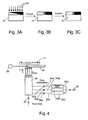
- FIG. 4schematically illustrates combinatorial synthesis of a compound on a thermally controlled substrate 51 using chemical vapor deposition (CVD) to provide in situ or multilayer deposition for combinatorial synthesis.
- a carrier gas source 52provides a carrier gas (preferably inert) that is passed through a selected number of one or more precursor evaporators or “bubblers”, 53 A, 53 B and 53 C, that provide the active vapor substance(s), 54 A, 54 B and 54 C, for CVD, either simultaneously or sequentially.
- the active vapors, 54 A, 54 B and 54 Cpass through corresponding flow controllers, 55 A, 55 B and 55 C, that determine the active vapor flow rates of the respective vapors at any given time.
- the active vaporsenter a pre-deposition chamber 56 and are moved axially along the chamber by a push gas provided by a push gas source 57 .
- the mask 58is fixed in location and a substrate stepper motor or other substrate movement device 59 moves the substrate 51 transversely.
- the mask movement device 59 and substrate movement device 60independently move the substrate 51 and the mask 58 transversely at the same time.
- the mix of active vapors 54 S that issues from the pre-deposition chamber 56can be closely controlled as a function of time.
- the coefficients b1 and b2may be positive and negative, respectively, so that the relative or absolute concentrations of the vapors 54 A and 54 B are increasing and decreasing, respectively, as the coordinate x increases, as illustrated in FIG. 5 A.
- the linear changes in concentration with the coordinate x in Eqs. (4A)-(4C)may be replaced by nonlinear changes in one or more of the quantities f(x; 54 S) by appropriate control of the flow controllers 55 A- 55 C and of the location of the movable mask 58 .
- FIG. 5 BOne possible result of such nonlinear deposition is shown in FIG. 5 B. If a uniform concentration of an active vapor 54 S is desired, the substrate 51 can be rotated during the time(s) this vapor is deposited.
- One or both of the concentrations of the deposited vapors 54 A and 54 Bmay be linear or may be nonlinear.
- Combinatorial deposition of two or more vapors 54 Soccurs by CVD, either one layer at a time or simultaneously, producing a multilayer or an in situ deposition, in the apparatus shown in FIG. 4 .
- each active vapor 54 Scan be (1) a solid or liquid substance packed into the corresponding evaporator 53 S, (2) a solid powder or liquid dissolved into an organic solvent or (3) any other source that will provide a vapor substance of the desired precursor when heated to a temperature in a selected temperature range.
- vaporizer temperature and flow rate of the carrier gascan be used to control the rate of delivery of a precursor.
- source (2)is present, the rate of delivery of a precursor is controlled by vaporizer temperature, carrier gas flow rate and pumping rate of the precursor solution into the corresponding vaporizer unit, such as 53 A.
- Combinatorial deposition on a substrate 61can also be performed by in situ co-deposition, using the apparatus shown in FIGS. 6A and 6B .
- the relative mix of vapors 64 Smay vary from one time to another time, and the slot(s) 67 need not move at a uniform rate across the exposed surface of the substrate 61 .
- the width w slot (t) of a slot or aperturemay vary according to a selected function with time t so that the slot aperture is wider at some times than at other times and may close altogether at one or more times. If the slot width w slot (t) is fixed and the rate v(t) at which the slot moves across the exposed surface of the substrate 61 is uniform, in situ co-deposition of two vapors with constant concentration gradients can be obtained, as illustrated in FIG. 5A , by varying the relative concentrations of the vapors 64 A and 64 B with time.
- This approachwill produce a chemical mixture of ( 64 A) u(x) ( 64 B) (1 ⁇ u(x)) as x varies from 0 to L across the exposed surface of the substrate 61 , with the index u(x) increasing or decreasing, linearly or nonlinearly, with increasing x.
- the concentration fractions of the two or more components, 64 A and 64 Bmay also be arranged to vary nonlinearly, as illustrated in FIG. 5 B.
- the masks 68 - 1 and 68 - 2are fixed in location and a substrate stepper motor or other substrate movement device 70 moves the substrate 51 transversely.
- the mask movement devices 69 - 1 and 69 - 2 and the substrate movement device 70independently move the substrate 51 and the masks, 58 - 1 and 58 - 2 , transversely relative to the direction of the flux f 64S .
- the in situ co-deposition process illustrated in FIGS. 6A and 6Bcan also be applied to co-sputtering, to co-evaporation, to co-ablation (e.g., using a laser ablating source), and to molecular beam epitaxy (MBE).
- MBEmolecular beam epitaxy
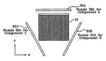
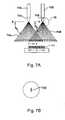
- FIG. 7Aillustrates another co-deposition approach, using two or more nuzzle slits, 75 A and 75 B, located at the exits of two vapor source chambers, 73 A and 73 B, respectively.
- Vapors, 74 A and 74 B, that exit through the nuzzle slits, 75 A and 75 B,may be arranged to vary independently in a linear or nonlinear manner with respective angles, ⁇ A and ⁇ B, measured relative to a reference line RR such as shown in FIG. 7 A.
- FIG. 7 Aillustrates another co-deposition approach, using two or more nuzzle slits, 75 A and 75 B, located at the exits of two vapor source chambers, 73 A and 73 B, respectively.
- Vapors, 74 A and 74 B, that exit through the nuzzle slits, 75 A and 75 Bmay be arranged to vary independently in a linear or nonlinear manner with respective angles, ⁇ A and ⁇ B, measured relative to a reference line RR
- FIG. 7Bschematically illustrates a nuzzle slit, in which a throat associated with the slit is shaped to produce a desired relative flow rate ⁇ ( ⁇ ) that varies in a controllable manner with an angle ⁇ , measured relative to a reference line.
- a nuzzle slitis a garden hose nozzle, in which movement of a small flow obstruction changes the spread of water that issues from the hose.
- Thiswill provide a linearly varying co-deposition mix on the exposed surface of the substrate 71 of ( 74 A) (x/L) ( 74 B) (1-x/L) as the coordinate x varies from 0 to x/L.
- An ultrasonic nuzzlecan be used for the apparatus shown in FIGS. 7A and 7B .
- a CVD approachis suitable where the precursor vapors can be pressurized and deposited according to the linear patterns in Eqs. (7A) and (7B).
- the nuzzle approachmay be difficult to apply using ion beam sputtering, co-sputtering, co-evaporation, co-ablation and MBE, because the precursor particles used in these processes are generated by point sources and the normal deposition profile on a substrate is Gaussian, rather than varying linearly with the coordinate x.
- a magnetron sputtering guncan be constructed to provide a nuzzle configuration.
- Ion beam depositionfor example, as developed by SKION Corporation in Hoboken, N.J., can also be used with this approach to deposit C, Si, Ni, Cu and other metals and alloys, using an electrical field to control the initial velocity of the ion that issues from the ion beam sputtering source.
- Three nuzzle slitsmay be arranged at the vertices of, or along three sides of, a general triangle, not necessarily isosceles or equilateral.
- FIGS. 10A and 10Billustrate, schematically and graphically, an embodiment of the invention.
- a chemical component source 91provides a chemical component, denoted A, that is to be deposited on a substrate 99 .
- the source 91provides a flux f A of the chemical component A that is approximately uniform in a selected coordinate direction z. If the flux f A is not approximately uniform in a plane ⁇ perpendicular to the z-direction, but is known as a function of the Cartesian coordinates, x and y, measured in the plane ⁇ , the details of this embodiment can be varied to achieve substantially the same result. Alternatively, a portion of the flux f A from the source can be masked to provide an approximately uniform flux through the mask aperture(s).
- the mask 93is spaced apart from the substrate 99 by a distance s2.
- the space 97 between the mask 93 and the substrate 99is either evacuated to a high vacuum or is filled with a selected gas at a selected low density ⁇ 97.
- the aperture 95 -ihas an aperture width di in a selected x-direction, and two adjacent apertures, such as 95 - 2 and 95 - 3 , have a selected aperture spacing distance D(2,3).
- the aperture spacings D(i,i+1)are uniform.
- the aperture spacings D(i,i+1)are variable according to the substrate deposition pattern desired. If a single aperture 95 -i receives the flux f A from the source 91 , the precursor particles A passed through the mask 93 at the aperture 95 -i will arrive at and deposit on the substrate 99 in an approximately Gaussian or normally distributed concentration pattern C(x;i), as a function of the transverse coordinate x, as illustrated in FIG. 10 B.
- , (9B) or to obey a more general power law C ( x )a′+b′ ⁇
- concentration envelope C(x)(or C(x,y)) produced will depend upon the parameters di (aperture widths), D(i,i+1) (aperture spacings), s1 (source-to-mask spacing), s2 (mask to substrate spacing), the gas, if any, and its density ⁇ 97 in the space 101 , the range of flux f A of the chemical component A produced in the z-direction by the source 91 , and other parameters describing the source.
- the concentration envelope C(x) shown in FIG. 10Bmay be reproduced in one direction only, if each aperture 95 -i in the mask is uniform in a second transverse coordinate direction y to produce a concentration envelope C(x,y) that depends non-trivially on each of the coordinates x and y.
- Each chemical component A, B, . . . to be deposited on the substratemay have a different mask with a different aperture pattern and may have different separation distances, s1 and s2.
- two chemical components, A and Bmay (but need not) use the same mask and/or the same separation distances, s1 and s2.
- FIG. 11Aillustrates use of two sources, 101 A and 101 B, each with its own component mask, 103 A and 103 B, which are optionally part of an overall mask 103 , positioned between the two sources and a substrate 109 .
- concentration envelope C(x;A;B)which is a sum of the concentration envelopes C(x;A) and C(x;B) shown in FIG. 11 B.
- two or more chemical components, A, B, . . . , each with its own source 111 A, 111 B, etc.can be simultaneously deposited on a single substrate 119 , as illustrated in FIG. 12.
- a single mask 113having suitable aperture widths and aperture spacings (not shown explicitly in FIG. 12 ), is positioned transverse to a direct path or line of sight from at least one source 111 A, 111 B, etc. to the common substrate 119 .
- the first source 111 A and mask 113produce a first concentration envelope C(x;A) on the substrate 119 ; and the second source 111 B and mask 113 produce a second concentration envelope C(x;B) on the substrate 119 .
- each of two or more sources, 121 A, 121 B and 121 C, arranged adjacent to and above two or more sides of a polygonmay have its own mask, 123 A, 123 B and 123 C, respectively, and each source mask combination will produce a different two-dimensional concentration envelope, C1(x,y;A) and C(x,y;B) and C(x,y;C), on a common substrate 129 that is positioned adjacent to the sources, with the masks being located between the sources and the substrate.
- each of the maskscan be separately designed, and thus optimized, for the particular concentration envelope desired for that chemical component.
- FIG. 14illustrates an alternative arrangement of the system in FIG. 13 , in which sources, 131 A, 131 B and 131 C, are located adjacent to and above two or more vertices of a polygon, and masks, 133 A, 133 B and 133 C, are located between a common substrate 139 and the respective sources.
- FIG. 15is a flow chart generally illustrating the processes used to practice the invention.
- first and second fluxes of respective first and second chemical componentsare directed toward a substrate.
- a maskhaving at least one opening (e.g., an aperture or an edge) is provided across the flux field that allows first and second selected portions of the respective first and second chemical components to be deposited on selected first and second portions of the substrate surface.
- the maskis moved transversely to at least one of the first and second flux directions at a selected movement rate, to provide a desired concentration of the first and second components on the substrate surface.
Landscapes
- Chemical & Material Sciences (AREA)
- Organic Chemistry (AREA)
- Chemical Kinetics & Catalysis (AREA)
- Engineering & Computer Science (AREA)
- Materials Engineering (AREA)
- Mechanical Engineering (AREA)
- Metallurgy (AREA)
- General Chemical & Material Sciences (AREA)
- Physical Vapour Deposition (AREA)
- Chemical Vapour Deposition (AREA)
Abstract
Description
Δt(tot)=Δt(x;A)+Δt(x;B) (1)
any location (x) on the substrate is exposed will be the same, no matter how the mask is moved from left (where REM and LES correspond) to right (where LEM and RES correspond).
w(x)=∫102[x−s(t)]dt/Δt(tot), (2)
here s(t) (0≦s(t)≦SL; 0≦t≦Δt(tot)) is the x coordinate of the right end REM of the
and the integral extends over the time interval 0≦t≦Δt(tot).
f(x;54A)=a1+b1·x, (4A)
f(x;54B)=a2+b2·x, (4B)
f(x;54C)=a3+b3·x, (4C)
where the magnitudes and signums of the coefficients a1, a2, a3, b1, b2 and b3 are independently chosen, subject to the constraint
0≦f(x;54A)+f(x;54B)+f(x;54C)≦1 (0≦×≦L). (5)
For example, the coefficients b1 and b2 may be positive and negative, respectively, so that the relative or absolute concentrations of the
where b1 and b2 are selected constant coefficients. The deposition rates, g(x;74A) and g(x;74B), of the respective vapors,74A and74B, on the
g(x;74A)=a1+b1·x (7A)
g(x;74B)=a2+b2·x (7B)
where a1 and a2 are appropriate constant coefficients. This will provide a linearly varying co-deposition mix on the exposed surface of the
f(x,y;A;B;C)=(84A)h(x,y;A)(84B)h(x,y;B)(84C)h(x,y;C), (8)
where h(x,y;A), h(x,y;B) and h(x,y;C) are two-dimensional distributions that are determined by the designs of the nuzzle slits85A,85B and85C, respectively. Three nuzzle slits may be arranged at the vertices of, or along three sides of, a general triangle, not necessarily isosceles or equilateral.
C(x)=a+b·x (9A)
or to be linear-symmetric,
C(x)=a+b|x|, (9B)
or to obey a more general power law
C(x)=a′+b′·|x|q(q≠0), (9C)
where a, b, a′, b′ and q are selected real numbers. The particular concentration envelope C(x) (or C(x,y)) produced will depend upon the parameters di (aperture widths), D(i,i+1) (aperture spacings), s1 (source-to-mask spacing), s2 (mask to substrate spacing), the gas, if any, and its density ρ97 in the space101, the range of flux fAof the chemical component A produced in the z-direction by the
C(x)=∫F(x′)Ap(x′)H(x-x′)dx′, (10)
where F(x′) represents the A particle flux fAand Ap(x′) is a mask characteristic function (=1 where a mask aperture is present; =0 where no mask aperture is present). The presence of the faltung function H(x-x′) in the integrand in Eq. (10) accounts for the fact that an A component particle that passes through the mask at a transverse location coordinate x′ may become deposited on the substrate at another transverse location coordinate x, due to scattering, initial velocity vector of the particle and other interference phenomena. A suitable approximation for a faltung function for a single aperture is
H(w)=(2πσ2)−1/2exp{−w2/2σ2}, (11)
where the parameter σ (having the units of length) characterizes the transverse spread of flux through a single aperture. Invoking the superposition principle, this faltung function, with possibly a different σ parameter, may be used for each aperture in the mask.
f(x;A;B)=[A]·C(x;A)+[B]·C(x;B), (12)
defines the total concentration of the chemical components, A and B, deposited on the substrate. Subsequent processing of the coated substrate, for example, by thermally driven diffusion, may produce a concentration pattern that differs from the initial total concentration envelope f(x;A;B).
Claims (9)
Priority Applications (6)
| Application Number | Priority Date | Filing Date | Title |
|---|---|---|---|
| US09/566,866US6911129B1 (en) | 2000-05-08 | 2000-05-08 | Combinatorial synthesis of material chips |
| PCT/US2001/014979WO2001085364A1 (en) | 2000-05-08 | 2001-05-08 | Combinatorial synthesis of material chips |
| EP01935206AEP1286790A4 (en) | 2000-05-08 | 2001-05-08 | Combinatorial synthesis of material chips |
| AU2001261319AAU2001261319A1 (en) | 2000-05-08 | 2001-05-08 | Combinatorial synthesis of material chips |
| JP2001582010AJP2003532794A (en) | 2000-05-08 | 2001-05-08 | Combinatorial synthesis of material chips |
| US11/054,003US20050166850A1 (en) | 2000-05-08 | 2005-02-08 | Combinatorial synthesis of material chips |
Applications Claiming Priority (1)
| Application Number | Priority Date | Filing Date | Title |
|---|---|---|---|
| US09/566,866US6911129B1 (en) | 2000-05-08 | 2000-05-08 | Combinatorial synthesis of material chips |
Related Child Applications (1)
| Application Number | Title | Priority Date | Filing Date |
|---|---|---|---|
| US11/054,003ContinuationUS20050166850A1 (en) | 2000-05-08 | 2005-02-08 | Combinatorial synthesis of material chips |
Publications (1)
| Publication Number | Publication Date |
|---|---|
| US6911129B1true US6911129B1 (en) | 2005-06-28 |
Family
ID=24264721
Family Applications (2)
| Application Number | Title | Priority Date | Filing Date |
|---|---|---|---|
| US09/566,866Expired - Fee RelatedUS6911129B1 (en) | 2000-05-08 | 2000-05-08 | Combinatorial synthesis of material chips |
| US11/054,003AbandonedUS20050166850A1 (en) | 2000-05-08 | 2005-02-08 | Combinatorial synthesis of material chips |
Family Applications After (1)
| Application Number | Title | Priority Date | Filing Date |
|---|---|---|---|
| US11/054,003AbandonedUS20050166850A1 (en) | 2000-05-08 | 2005-02-08 | Combinatorial synthesis of material chips |
Country Status (5)
| Country | Link |
|---|---|
| US (2) | US6911129B1 (en) |
| EP (1) | EP1286790A4 (en) |
| JP (1) | JP2003532794A (en) |
| AU (1) | AU2001261319A1 (en) |
| WO (1) | WO2001085364A1 (en) |
Cited By (30)
| Publication number | Priority date | Publication date | Assignee | Title |
|---|---|---|---|---|
| US20050051517A1 (en)* | 2003-08-12 | 2005-03-10 | Oehrlein Gottlieb S. | Method and system for nanoscale plasma processing of objects |
| US20060057240A1 (en)* | 2002-09-20 | 2006-03-16 | Hideomi Koinuma | Masking mechanism for film-forming device |
| US20060060301A1 (en)* | 2004-09-17 | 2006-03-23 | Lazovsky David E | Substrate processing using molecular self-assembly |
| US20060108320A1 (en)* | 2004-11-22 | 2006-05-25 | Lazovsky David E | Molecular self-assembly in substrate processing |
| US20060261434A1 (en)* | 2005-05-18 | 2006-11-23 | Intermolecular Inc. | Formation of a masking layer on a dielectric region to facilitate formation of a capping layer on electrically conductive regions separated by the dielectric region |
| US20060264020A1 (en)* | 2005-05-18 | 2006-11-23 | Intermolecular Inc. | Formation of a masking layer on a dielectric region to facilitate formation of a capping layer on electrically conductive regions separated by the dielectric region |
| US20060292846A1 (en)* | 2004-09-17 | 2006-12-28 | Pinto Gustavo A | Material management in substrate processing |
| US20060292845A1 (en)* | 2004-09-17 | 2006-12-28 | Chiang Tony P | Processing substrates using site-isolated processing |
| US20070082508A1 (en)* | 2005-10-11 | 2007-04-12 | Chiang Tony P | Methods for discretized processing and process sequence integration of regions of a substrate |
| US20070082485A1 (en)* | 2005-10-11 | 2007-04-12 | Chiang Tony P | Methods for discretized formation of masking and capping layers on a substrate |
| US20070089857A1 (en)* | 2005-10-11 | 2007-04-26 | Chiang Tony P | Systems for discretized processing of regions of a substrate |
| US20070166989A1 (en)* | 2005-05-18 | 2007-07-19 | Intermolecular, Inc. | Substrate processing including a masking layer |
| US20070202610A1 (en)* | 2006-02-10 | 2007-08-30 | Chiang Tony P | Method and apparatus for combinatorially varying materials, unit process and process sequence |
| US20070199510A1 (en)* | 2006-02-24 | 2007-08-30 | Weiner Kurt H | Systems and methods for sealing in site-isolated reactors |
| US20070267631A1 (en)* | 2006-05-18 | 2007-11-22 | Intermolecular, Inc. | System and Method for Increasing Productivity of Combinatorial Screening |
| US20080020589A1 (en)* | 2006-07-19 | 2008-01-24 | Chiang Tony P | Method and system for isolated and discretized process sequence integration |
| US20080035057A1 (en)* | 2004-12-27 | 2008-02-14 | Asml Holding N.V. | Method and Apparatus for Creating a Phase Step in Mirrors Used in Spatial Light Modulator Arrays |
| US20080156769A1 (en)* | 2006-12-29 | 2008-07-03 | Intermolecular, Inc. | Advanced mixing system for integrated tool having site-isolated reactors |
| US20100155224A1 (en)* | 2004-03-19 | 2010-06-24 | United Technologies Corporation | Multi-Component Deposition |
| US20130125818A1 (en)* | 2011-11-22 | 2013-05-23 | Intermolecular, Inc. | Combinatorial deposition based on a spot apparatus |
| US8575027B1 (en) | 2012-06-26 | 2013-11-05 | Intermolecular, Inc. | Sputtering and aligning multiple layers having different boundaries |
| US20140174907A1 (en)* | 2012-12-21 | 2014-06-26 | Intermolecular, Inc. | High Deposition Rate Chamber with Co-Sputtering Capabilities |
| US8882917B1 (en)* | 2009-12-31 | 2014-11-11 | Intermolecular, Inc. | Substrate processing including correction for deposition location |
| US8974695B2 (en) | 2010-11-11 | 2015-03-10 | Auterra, Inc. | Phosphors of rare earth and transition metal doped Ca1+xSr1-xGayIn2-ySzSe3-zF2; manufacturing and applications |
| WO2015140731A1 (en)* | 2014-03-18 | 2015-09-24 | 3D-Oxides | Deposition process based on stencil mask and application to the fabrication of tags supporting multi-functional traceable codes |
| WO2016210010A1 (en)* | 2015-06-23 | 2016-12-29 | Ningbo Infinite Materials Technology Co., Ltd. | A high-throughput combinatorial materials experimental apparatus for in-situ synthesis and real-time characterization and related methods |
| CN108060397A (en)* | 2017-12-25 | 2018-05-22 | 浙江工业大学 | A kind of surface graded film preparation device based on chaotic source material |
| US10066160B2 (en) | 2015-05-01 | 2018-09-04 | Intematix Corporation | Solid-state white light generating lighting arrangements including photoluminescence wavelength conversion components |
| US20180277797A1 (en)* | 2002-03-26 | 2018-09-27 | Rohm Company, Ltd. | Organic electroluminescent device |
| US11193198B2 (en)* | 2018-12-17 | 2021-12-07 | Applied Materials, Inc. | Methods of forming devices on a substrate |
Families Citing this family (12)
| Publication number | Priority date | Publication date | Assignee | Title |
|---|---|---|---|---|
| WO2002024321A1 (en)* | 2000-09-22 | 2002-03-28 | General Electric Company | Combinatorial coating systems and methods |
| US7635564B2 (en) | 2002-10-25 | 2009-12-22 | Agilent Technologies, Inc. | Biopolymeric arrays having replicate elements |
| US8084102B2 (en)* | 2007-02-06 | 2011-12-27 | Sion Power Corporation | Methods for co-flash evaporation of polymerizable monomers and non-polymerizable carrier solvent/salt mixtures/solutions |
| US8334015B2 (en)* | 2007-09-05 | 2012-12-18 | Intermolecular, Inc. | Vapor based combinatorial processing |
| US8129288B2 (en)* | 2008-05-02 | 2012-03-06 | Intermolecular, Inc. | Combinatorial plasma enhanced deposition techniques |
| KR100991131B1 (en)* | 2010-06-01 | 2010-11-01 | 김상영 | Method for gradational deposition using vaccum device |
| GB2493022B (en)* | 2011-07-21 | 2014-04-23 | Ilika Technologies Ltd | Vapour deposition process for the preparation of a phosphate compound |
| EP2776602A4 (en)* | 2011-11-11 | 2015-06-24 | Veeco Instr Inc | Ion beam deposition of fluorine-based optical films |
| JP6077906B2 (en)* | 2013-03-28 | 2017-02-08 | 株式会社アツミテック | Sputtering equipment |
| CN106637087B (en)* | 2016-11-18 | 2019-05-17 | 上海天马微电子有限公司 | Evaporation plating equipment |
| US12180610B2 (en)* | 2023-01-09 | 2024-12-31 | Wisconsin Alumni Research Foundation | Hybrid pulsed laser deposition of complex oxide thin films made from elements having a large vapor pressure mismatch |
| US20250215548A1 (en)* | 2024-01-03 | 2025-07-03 | Entegris, Inc. | Multi-metal oxide coatings, related devices and methods |
Citations (8)
| Publication number | Priority date | Publication date | Assignee | Title |
|---|---|---|---|---|
| US3193408A (en) | 1961-08-22 | 1965-07-06 | David P Triller | Method for producing integrated circuitry components |
| US4591417A (en) | 1983-12-27 | 1986-05-27 | Ford Motor Company | Tandem deposition of cermets |
| US5097800A (en) | 1983-12-19 | 1992-03-24 | Spectrum Control, Inc. | High speed apparatus for forming capacitors |
| WO1996011878A1 (en) | 1994-10-18 | 1996-04-25 | The Regents Of The University Of California | The combinatorial synthesis of novel materials |
| US6045671A (en)* | 1994-10-18 | 2000-04-04 | Symyx Technologies, Inc. | Systems and methods for the combinatorial synthesis of novel materials |
| WO2000043119A1 (en) | 1999-01-26 | 2000-07-27 | Symyx Technologies, Inc. | Programmable apparatus for graded composition coating by co-deposition |
| WO2000048725A1 (en) | 1999-02-17 | 2000-08-24 | Oxxel Oxide Electronics Technology, Inc. | Method for preparation of libraries using a combinatorial molecular beam epitaxy (combe) apparatus |
| WO2000058003A1 (en) | 1999-03-31 | 2000-10-05 | General Electric Company | Method for preparing and screening catalysts |
Family Cites Families (14)
| Publication number | Priority date | Publication date | Assignee | Title |
|---|---|---|---|---|
| JPS4942155U (en)* | 1972-04-24 | 1974-04-13 | ||
| US4102768A (en)* | 1972-11-29 | 1978-07-25 | Triplex Safety Glass Company Limited | Metal oxide coatings |
| JPS5133779A (en)* | 1974-09-17 | 1976-03-23 | Victor Company Of Japan | Jochakumakuso no sekisojochakuhoho |
| JPS5721670U (en)* | 1980-07-09 | 1982-02-04 | ||
| JPS6059561B2 (en)* | 1980-11-12 | 1985-12-25 | 日本板硝子株式会社 | Method for forming thin films with composition distribution |
| JPS58224169A (en)* | 1982-06-22 | 1983-12-26 | Nippon Sheet Glass Co Ltd | Method for forming thin film having refractive index distribution |
| JPS619574A (en)* | 1984-06-25 | 1986-01-17 | Nippon Telegr & Teleph Corp <Ntt> | Vacuum vapor deposition device |
| JPS6342370A (en)* | 1986-08-06 | 1988-02-23 | Nec Corp | Control device for thickness of vapor deposited film |
| GB8627308D0 (en)* | 1986-11-14 | 1986-12-17 | Alcan Int Ltd | Composite metal deposit |
| JPH02247372A (en)* | 1989-03-17 | 1990-10-03 | Mitsubishi Electric Corp | Thin film deposition method |
| JPH0471183A (en)* | 1990-07-12 | 1992-03-05 | Canon Inc | Manufacture of panel heater |
| JPH062109A (en)* | 1992-06-17 | 1994-01-11 | Kobe Steel Ltd | Al-nb alloy plated material, al-nb laminate plated material and production of the materials |
| JPH07180056A (en)* | 1993-12-24 | 1995-07-18 | Kobe Steel Ltd | Production of vapor deposition plating material |
| JPH0987828A (en)* | 1995-09-28 | 1997-03-31 | Murata Mfg Co Ltd | Formation of electrode of electronic part and device used for the same |
- 2000
- 2000-05-08USUS09/566,866patent/US6911129B1/ennot_activeExpired - Fee Related
- 2001
- 2001-05-08JPJP2001582010Apatent/JP2003532794A/enactivePending
- 2001-05-08EPEP01935206Apatent/EP1286790A4/ennot_activeWithdrawn
- 2001-05-08WOPCT/US2001/014979patent/WO2001085364A1/enactiveApplication Filing
- 2001-05-08AUAU2001261319Apatent/AU2001261319A1/ennot_activeAbandoned
- 2005
- 2005-02-08USUS11/054,003patent/US20050166850A1/ennot_activeAbandoned
Patent Citations (8)
| Publication number | Priority date | Publication date | Assignee | Title |
|---|---|---|---|---|
| US3193408A (en) | 1961-08-22 | 1965-07-06 | David P Triller | Method for producing integrated circuitry components |
| US5097800A (en) | 1983-12-19 | 1992-03-24 | Spectrum Control, Inc. | High speed apparatus for forming capacitors |
| US4591417A (en) | 1983-12-27 | 1986-05-27 | Ford Motor Company | Tandem deposition of cermets |
| WO1996011878A1 (en) | 1994-10-18 | 1996-04-25 | The Regents Of The University Of California | The combinatorial synthesis of novel materials |
| US6045671A (en)* | 1994-10-18 | 2000-04-04 | Symyx Technologies, Inc. | Systems and methods for the combinatorial synthesis of novel materials |
| WO2000043119A1 (en) | 1999-01-26 | 2000-07-27 | Symyx Technologies, Inc. | Programmable apparatus for graded composition coating by co-deposition |
| WO2000048725A1 (en) | 1999-02-17 | 2000-08-24 | Oxxel Oxide Electronics Technology, Inc. | Method for preparation of libraries using a combinatorial molecular beam epitaxy (combe) apparatus |
| WO2000058003A1 (en) | 1999-03-31 | 2000-10-05 | General Electric Company | Method for preparing and screening catalysts |
Cited By (63)
| Publication number | Priority date | Publication date | Assignee | Title |
|---|---|---|---|---|
| US10998527B2 (en)* | 2002-03-26 | 2021-05-04 | Rohm Co., Ltd. | Organic electroluminescent device |
| US20180277797A1 (en)* | 2002-03-26 | 2018-09-27 | Rohm Company, Ltd. | Organic electroluminescent device |
| US10217967B2 (en) | 2002-03-26 | 2019-02-26 | Rohm Co., Ltd. | Organic electroluminescent device |
| US10312474B2 (en) | 2002-03-26 | 2019-06-04 | Rohm Co., Ltd. | Organic electroluminescent device comprising a plurality of light emissive units |
| US10319949B2 (en) | 2002-03-26 | 2019-06-11 | Rohm Co., Ltd. | Organic electroluminescent device |
| US20100151128A1 (en)* | 2002-09-20 | 2010-06-17 | Japan Science And Technology Agency | Masking mechanism for film forming apparatus |
| US20060057240A1 (en)* | 2002-09-20 | 2006-03-16 | Hideomi Koinuma | Masking mechanism for film-forming device |
| US9157144B2 (en)* | 2002-09-20 | 2015-10-13 | Japan Science And Technology Agency | Masking mechanism for film forming apparatus |
| US7470329B2 (en)* | 2003-08-12 | 2008-12-30 | University Of Maryland | Method and system for nanoscale plasma processing of objects |
| US20050051517A1 (en)* | 2003-08-12 | 2005-03-10 | Oehrlein Gottlieb S. | Method and system for nanoscale plasma processing of objects |
| US20100155224A1 (en)* | 2004-03-19 | 2010-06-24 | United Technologies Corporation | Multi-Component Deposition |
| US8864956B2 (en)* | 2004-03-19 | 2014-10-21 | United Technologies Corporation | Multi-component deposition |
| US20060060301A1 (en)* | 2004-09-17 | 2006-03-23 | Lazovsky David E | Substrate processing using molecular self-assembly |
| US20060292846A1 (en)* | 2004-09-17 | 2006-12-28 | Pinto Gustavo A | Material management in substrate processing |
| US20060292845A1 (en)* | 2004-09-17 | 2006-12-28 | Chiang Tony P | Processing substrates using site-isolated processing |
| US8882914B2 (en) | 2004-09-17 | 2014-11-11 | Intermolecular, Inc. | Processing substrates using site-isolated processing |
| US20060108320A1 (en)* | 2004-11-22 | 2006-05-25 | Lazovsky David E | Molecular self-assembly in substrate processing |
| US7309658B2 (en) | 2004-11-22 | 2007-12-18 | Intermolecular, Inc. | Molecular self-assembly in substrate processing |
| US20080035057A1 (en)* | 2004-12-27 | 2008-02-14 | Asml Holding N.V. | Method and Apparatus for Creating a Phase Step in Mirrors Used in Spatial Light Modulator Arrays |
| US20070166989A1 (en)* | 2005-05-18 | 2007-07-19 | Intermolecular, Inc. | Substrate processing including a masking layer |
| US8030772B2 (en) | 2005-05-18 | 2011-10-04 | Intermolecular, Inc. | Formation of a masking layer on a dielectric region to facilitate formation of a capping layer on electrically conductive regions separated by the dielectric region |
| US7390739B2 (en) | 2005-05-18 | 2008-06-24 | Lazovsky David E | Formation of a masking layer on a dielectric region to facilitate formation of a capping layer on electrically conductive regions separated by the dielectric region |
| US7879710B2 (en) | 2005-05-18 | 2011-02-01 | Intermolecular, Inc. | Substrate processing including a masking layer |
| US20080246150A1 (en)* | 2005-05-18 | 2008-10-09 | Lazovsky David E | Formation of a masking layer on a dielectric region to facilitate formation of a capping layer on electrically conductive regions separated by the dielectric region |
| US20060264020A1 (en)* | 2005-05-18 | 2006-11-23 | Intermolecular Inc. | Formation of a masking layer on a dielectric region to facilitate formation of a capping layer on electrically conductive regions separated by the dielectric region |
| US7749881B2 (en) | 2005-05-18 | 2010-07-06 | Intermolecular, Inc. | Formation of a masking layer on a dielectric region to facilitate formation of a capping layer on electrically conductive regions separated by the dielectric region |
| US20060261434A1 (en)* | 2005-05-18 | 2006-11-23 | Intermolecular Inc. | Formation of a masking layer on a dielectric region to facilitate formation of a capping layer on electrically conductive regions separated by the dielectric region |
| US7902063B2 (en) | 2005-10-11 | 2011-03-08 | Intermolecular, Inc. | Methods for discretized formation of masking and capping layers on a substrate |
| US8084400B2 (en) | 2005-10-11 | 2011-12-27 | Intermolecular, Inc. | Methods for discretized processing and process sequence integration of regions of a substrate |
| US8776717B2 (en) | 2005-10-11 | 2014-07-15 | Intermolecular, Inc. | Systems for discretized processing of regions of a substrate |
| US20070082508A1 (en)* | 2005-10-11 | 2007-04-12 | Chiang Tony P | Methods for discretized processing and process sequence integration of regions of a substrate |
| US20070089857A1 (en)* | 2005-10-11 | 2007-04-26 | Chiang Tony P | Systems for discretized processing of regions of a substrate |
| US20070082487A1 (en)* | 2005-10-11 | 2007-04-12 | Chiang Tony P | Methods for discretized processing of regions of a substrate |
| US20070082485A1 (en)* | 2005-10-11 | 2007-04-12 | Chiang Tony P | Methods for discretized formation of masking and capping layers on a substrate |
| US7544574B2 (en) | 2005-10-11 | 2009-06-09 | Intermolecular, Inc. | Methods for discretized processing of regions of a substrate |
| US20070202614A1 (en)* | 2006-02-10 | 2007-08-30 | Chiang Tony P | Method and apparatus for combinatorially varying materials, unit process and process sequence |
| US20070202610A1 (en)* | 2006-02-10 | 2007-08-30 | Chiang Tony P | Method and apparatus for combinatorially varying materials, unit process and process sequence |
| US7955436B2 (en) | 2006-02-24 | 2011-06-07 | Intermolecular, Inc. | Systems and methods for sealing in site-isolated reactors |
| US20070199510A1 (en)* | 2006-02-24 | 2007-08-30 | Weiner Kurt H | Systems and methods for sealing in site-isolated reactors |
| US8772772B2 (en) | 2006-05-18 | 2014-07-08 | Intermolecular, Inc. | System and method for increasing productivity of combinatorial screening |
| US20070267631A1 (en)* | 2006-05-18 | 2007-11-22 | Intermolecular, Inc. | System and Method for Increasing Productivity of Combinatorial Screening |
| US20080020589A1 (en)* | 2006-07-19 | 2008-01-24 | Chiang Tony P | Method and system for isolated and discretized process sequence integration |
| US20080017109A1 (en)* | 2006-07-19 | 2008-01-24 | Chiang Tony P | Method and system for isolated and discretized process sequence integration |
| US7867904B2 (en) | 2006-07-19 | 2011-01-11 | Intermolecular, Inc. | Method and system for isolated and discretized process sequence integration |
| US8815013B2 (en) | 2006-07-19 | 2014-08-26 | Intermolecular, Inc. | Method and system for isolated and discretized process sequence integration |
| US20120231975A1 (en)* | 2006-12-29 | 2012-09-13 | Intermolecular, Inc. | Advanced mixing system for integrated tool having site-isolated reactors |
| US20080156769A1 (en)* | 2006-12-29 | 2008-07-03 | Intermolecular, Inc. | Advanced mixing system for integrated tool having site-isolated reactors |
| US8011317B2 (en) | 2006-12-29 | 2011-09-06 | Intermolecular, Inc. | Advanced mixing system for integrated tool having site-isolated reactors |
| US8414703B2 (en)* | 2006-12-29 | 2013-04-09 | Intermolecular, Inc. | Advanced mixing system for integrated tool having site-isolated reactors |
| US8882917B1 (en)* | 2009-12-31 | 2014-11-11 | Intermolecular, Inc. | Substrate processing including correction for deposition location |
| US8974695B2 (en) | 2010-11-11 | 2015-03-10 | Auterra, Inc. | Phosphors of rare earth and transition metal doped Ca1+xSr1-xGayIn2-ySzSe3-zF2; manufacturing and applications |
| US20130125818A1 (en)* | 2011-11-22 | 2013-05-23 | Intermolecular, Inc. | Combinatorial deposition based on a spot apparatus |
| US8575027B1 (en) | 2012-06-26 | 2013-11-05 | Intermolecular, Inc. | Sputtering and aligning multiple layers having different boundaries |
| US20140174907A1 (en)* | 2012-12-21 | 2014-06-26 | Intermolecular, Inc. | High Deposition Rate Chamber with Co-Sputtering Capabilities |
| CN106460167A (en)* | 2014-03-18 | 2017-02-22 | 3D-奥克赛茨公司 | Stencil-mask-based deposition method and its application in the manufacture of labels carrying multifunctional traceable codes |
| US10280506B2 (en) | 2014-03-18 | 2019-05-07 | 3D-Oxides | Deposition process based on stencil mask and application to the fabrication of tags supporting multi-functional traceable codes |
| CN110079783A (en)* | 2014-03-18 | 2019-08-02 | 3D-奥克赛茨公司 | Label apparatus, its purposes and the packaging for label apparatus |
| WO2015140731A1 (en)* | 2014-03-18 | 2015-09-24 | 3D-Oxides | Deposition process based on stencil mask and application to the fabrication of tags supporting multi-functional traceable codes |
| US10066160B2 (en) | 2015-05-01 | 2018-09-04 | Intematix Corporation | Solid-state white light generating lighting arrangements including photoluminescence wavelength conversion components |
| WO2016210010A1 (en)* | 2015-06-23 | 2016-12-29 | Ningbo Infinite Materials Technology Co., Ltd. | A high-throughput combinatorial materials experimental apparatus for in-situ synthesis and real-time characterization and related methods |
| US10994256B2 (en) | 2015-06-23 | 2021-05-04 | Ningbo Infinite Materials Technology Co., Ltd. | High-throughput combinatorial materials experimental apparatus for in-situ synthesis and real-time characterization and related methods |
| CN108060397A (en)* | 2017-12-25 | 2018-05-22 | 浙江工业大学 | A kind of surface graded film preparation device based on chaotic source material |
| US11193198B2 (en)* | 2018-12-17 | 2021-12-07 | Applied Materials, Inc. | Methods of forming devices on a substrate |
Also Published As
| Publication number | Publication date |
|---|---|
| WO2001085364A1 (en) | 2001-11-15 |
| EP1286790A4 (en) | 2004-10-13 |
| WO2001085364A9 (en) | 2002-12-12 |
| AU2001261319A1 (en) | 2001-11-20 |
| US20050166850A1 (en) | 2005-08-04 |
| EP1286790A1 (en) | 2003-03-05 |
| JP2003532794A (en) | 2003-11-05 |
Similar Documents
| Publication | Publication Date | Title |
|---|---|---|
| US6911129B1 (en) | Combinatorial synthesis of material chips | |
| US6716656B2 (en) | Self-aligned hybrid deposition | |
| US7682660B2 (en) | Process and apparatus for organic vapor jet deposition | |
| EP0406871B1 (en) | Laser deposition method and apparatus | |
| JP2000503753A (en) | Systems and methods for combinatorial synthesis of new substances | |
| EP1423552B1 (en) | Process for organic vapor jet deposition | |
| CN104328391B (en) | Chemical beam thin film deposition apparatus and method for thin film deposition using the same | |
| US20130011440A1 (en) | Method and device for depositing thin layers, especially for the production of multiple layers, nanolayers, nanostructures and nanocomposites | |
| JPS6021955B2 (en) | Method and apparatus for growth of compound thin films | |
| US20050255242A1 (en) | Apparatus and method for high rate uniform coating, including non-line of sight | |
| US7592043B2 (en) | Method and apparatus for coating a patterned thin film on a substrate from a fluid source with continuous feed capability | |
| JP6656261B2 (en) | Apparatus for depositing vaporized material, distribution pipe, vacuum deposition chamber, and method for depositing vaporized material | |
| US6579420B2 (en) | Apparatus and method for uniformly depositing thin films over substrates | |
| US20080187683A1 (en) | Resonant infrared laser-assisted nanoparticle transfer and applications of same | |
| US20050205696A1 (en) | Deposition apparatus and method | |
| JP2005520687A (en) | Thin film deposition process and apparatus on a substrate | |
| CN113166925B (en) | Vapor source for depositing vaporized material, nozzle for vapor source, vacuum deposition system, and method for depositing vaporized material | |
| WO2003034471A1 (en) | Self-aligned hybrid deposition | |
| WO2009083193A2 (en) | Method and apparatus for surface treatment by combined particle irradiation | |
| JPS5822376A (en) | Method of forming heterogeneous optical thin films by reactive deposition | |
| KR101806414B1 (en) | Apparatus and method for film deposition | |
| JP2548387B2 (en) | Liquid crystal alignment film manufacturing equipment | |
| JP6543664B2 (en) | Vacuum deposition chamber | |
| Zachary et al. | Cluster beam deposition of metal, insulator, and semiconductor nanoparticles | |
| Autric et al. | Pulsed laser deposition of thin film materials in vacuum and in ambient gas conditions |
Legal Events
| Date | Code | Title | Description |
|---|---|---|---|
| AS | Assignment | Owner name:INTEMATIX CORPORATION, CALIFORNIA Free format text:ASSIGNMENT OF ASSIGNORS INTEREST;ASSIGNOR:LI, YI-QUN;REEL/FRAME:010791/0130 Effective date:20000508 | |
| FEPP | Fee payment procedure | Free format text:PAYOR NUMBER ASSIGNED (ORIGINAL EVENT CODE: ASPN); ENTITY STATUS OF PATENT OWNER: SMALL ENTITY | |
| FPAY | Fee payment | Year of fee payment:4 | |
| FPAY | Fee payment | Year of fee payment:8 | |
| AS | Assignment | Owner name:EAST WEST BANK, CALIFORNIA Free format text:SECURITY INTEREST;ASSIGNORS:INTEMATIX HONG KONG CO. LIMITED;INTEMATIX CORPORATION;REEL/FRAME:036967/0623 Effective date:20151022 | |
| REMI | Maintenance fee reminder mailed | ||
| LAPS | Lapse for failure to pay maintenance fees | ||
| STCH | Information on status: patent discontinuation | Free format text:PATENT EXPIRED DUE TO NONPAYMENT OF MAINTENANCE FEES UNDER 37 CFR 1.362 | |
| FP | Lapsed due to failure to pay maintenance fee | Effective date:20170628 | |
| AS | Assignment | Owner name:INTEMATIX CORPORATION, CALIFORNIA Free format text:RELEASE BY SECURED PARTY;ASSIGNOR:EAST WEST BANK;REEL/FRAME:059910/0304 Effective date:20220414 Owner name:INTEMATIX HONG KONG CO. LIMITED, CALIFORNIA Free format text:RELEASE BY SECURED PARTY;ASSIGNOR:EAST WEST BANK;REEL/FRAME:059910/0304 Effective date:20220414 |