US6910947B2 - Control of chemical mechanical polishing pad conditioner directional velocity to improve pad life - Google Patents
Control of chemical mechanical polishing pad conditioner directional velocity to improve pad lifeDownload PDFInfo
- Publication number
- US6910947B2 US6910947B2US09/998,372US99837201AUS6910947B2US 6910947 B2US6910947 B2US 6910947B2US 99837201 AUS99837201 AUS 99837201AUS 6910947 B2US6910947 B2US 6910947B2
- Authority
- US
- United States
- Prior art keywords
- conditioning
- pad
- wafer
- polishing
- removal rate
- Prior art date
- Legal status (The legal status is an assumption and is not a legal conclusion. Google has not performed a legal analysis and makes no representation as to the accuracy of the status listed.)
- Expired - Fee Related, expires
Links
- 238000005498polishingMethods0.000titleclaimsabstractdescription183
- 239000000126substanceSubstances0.000titleclaimsabstractdescription16
- 230000003750conditioning effectEffects0.000claimsabstractdescription331
- 239000000463materialSubstances0.000claimsabstractdescription135
- 238000000034methodMethods0.000claimsabstractdescription92
- 230000008569processEffects0.000claimsdescription36
- 238000005457optimizationMethods0.000claimsdescription17
- 238000011084recoveryMethods0.000claimsdescription16
- 230000001143conditioned effectEffects0.000claimsdescription10
- 238000013400design of experimentMethods0.000claimsdescription7
- 238000000418atomic force spectrumMethods0.000claimsdescription3
- 238000010408sweepingMethods0.000claimsdescription3
- 238000009987spinningMethods0.000claimsdescription2
- 235000012431wafersNutrition0.000description170
- 239000002002slurrySubstances0.000description14
- 230000006870functionEffects0.000description13
- 238000004519manufacturing processMethods0.000description9
- 230000007423decreaseEffects0.000description8
- 238000007517polishing processMethods0.000description8
- 239000000203mixtureSubstances0.000description7
- 238000012545processingMethods0.000description7
- 238000004422calculation algorithmMethods0.000description6
- 230000000694effectsEffects0.000description6
- 239000004065semiconductorSubstances0.000description6
- 238000004891communicationMethods0.000description5
- 239000002609mediumSubstances0.000description5
- 230000003746surface roughnessEffects0.000description5
- VYPSYNLAJGMNEJ-UHFFFAOYSA-NSilicium dioxideChemical compoundO=[Si]=OVYPSYNLAJGMNEJ-UHFFFAOYSA-N0.000description4
- 230000008859changeEffects0.000description4
- 238000010586diagramMethods0.000description4
- 238000005259measurementMethods0.000description4
- 230000003247decreasing effectEffects0.000description3
- 239000010408filmSubstances0.000description3
- 230000003287optical effectEffects0.000description3
- 230000004044responseEffects0.000description3
- 239000000758substrateSubstances0.000description3
- XLYOFNOQVPJJNP-UHFFFAOYSA-NwaterSubstancesOXLYOFNOQVPJJNP-UHFFFAOYSA-N0.000description3
- XUIMIQQOPSSXEZ-UHFFFAOYSA-NSiliconChemical compound[Si]XUIMIQQOPSSXEZ-UHFFFAOYSA-N0.000description2
- 230000003044adaptive effectEffects0.000description2
- 238000013459approachMethods0.000description2
- 230000015556catabolic processEffects0.000description2
- 238000006731degradation reactionMethods0.000description2
- 238000002474experimental methodMethods0.000description2
- 230000033001locomotionEffects0.000description2
- 238000004377microelectronicMethods0.000description2
- 229910052710siliconInorganic materials0.000description2
- 239000010703siliconSubstances0.000description2
- 239000000377silicon dioxideSubstances0.000description2
- 238000003860storageMethods0.000description2
- 238000012876topographyMethods0.000description2
- RYGMFSIKBFXOCR-UHFFFAOYSA-NCopperChemical compound[Cu]RYGMFSIKBFXOCR-UHFFFAOYSA-N0.000description1
- JOYRKODLDBILNP-UHFFFAOYSA-NEthyl urethaneChemical compoundCCOC(N)=OJOYRKODLDBILNP-UHFFFAOYSA-N0.000description1
- 229910052782aluminiumInorganic materials0.000description1
- XAGFODPZIPBFFR-UHFFFAOYSA-NaluminiumChemical compound[Al]XAGFODPZIPBFFR-UHFFFAOYSA-N0.000description1
- 230000005540biological transmissionEffects0.000description1
- 230000000903blocking effectEffects0.000description1
- 239000005380borophosphosilicate glassSubstances0.000description1
- 238000004364calculation methodMethods0.000description1
- 239000002131composite materialSubstances0.000description1
- 239000004020conductorSubstances0.000description1
- 229910052802copperInorganic materials0.000description1
- 239000010949copperSubstances0.000description1
- 238000013480data collectionMethods0.000description1
- 230000001934delayEffects0.000description1
- 238000013461designMethods0.000description1
- 238000011161developmentMethods0.000description1
- 239000003989dielectric materialSubstances0.000description1
- 238000009826distributionMethods0.000description1
- 230000003628erosive effectEffects0.000description1
- 238000011156evaluationMethods0.000description1
- 238000012625in-situ measurementMethods0.000description1
- 238000011850initial investigationMethods0.000description1
- 238000011835investigationMethods0.000description1
- 238000011326mechanical measurementMethods0.000description1
- 238000010297mechanical methods and processMethods0.000description1
- 230000005226mechanical processes and functionsEffects0.000description1
- 230000007246mechanismEffects0.000description1
- 229910052751metalInorganic materials0.000description1
- 239000002184metalSubstances0.000description1
- 150000002739metalsChemical class0.000description1
- 238000012986modificationMethods0.000description1
- 230000004048modificationEffects0.000description1
- 239000013307optical fiberSubstances0.000description1
- 230000002093peripheral effectEffects0.000description1
- 229920000642polymerPolymers0.000description1
- 238000004886process controlMethods0.000description1
- 230000000644propagated effectEffects0.000description1
- 239000012858resilient materialSubstances0.000description1
- 229920006395saturated elastomerPolymers0.000description1
- 230000008054signal transmissionEffects0.000description1
- 235000012239silicon dioxideNutrition0.000description1
- 238000007619statistical methodMethods0.000description1
- 239000013589supplementSubstances0.000description1
- -1thermal oxideChemical compound0.000description1
- 239000010409thin filmSubstances0.000description1
- 238000013519translationMethods0.000description1
- 239000006163transport mediaSubstances0.000description1
- WFKWXMTUELFFGS-UHFFFAOYSA-NtungstenChemical compound[W]WFKWXMTUELFFGS-UHFFFAOYSA-N0.000description1
- 229910052721tungstenInorganic materials0.000description1
- 239000010937tungstenSubstances0.000description1
- 239000002699waste materialSubstances0.000description1
- 238000005303weighingMethods0.000description1
Images


Classifications
- B—PERFORMING OPERATIONS; TRANSPORTING
- B24—GRINDING; POLISHING
- B24B—MACHINES, DEVICES, OR PROCESSES FOR GRINDING OR POLISHING; DRESSING OR CONDITIONING OF ABRADING SURFACES; FEEDING OF GRINDING, POLISHING, OR LAPPING AGENTS
- B24B37/00—Lapping machines or devices; Accessories
- B24B37/005—Control means for lapping machines or devices
- B24B37/013—Devices or means for detecting lapping completion
- B—PERFORMING OPERATIONS; TRANSPORTING
- B24—GRINDING; POLISHING
- B24B—MACHINES, DEVICES, OR PROCESSES FOR GRINDING OR POLISHING; DRESSING OR CONDITIONING OF ABRADING SURFACES; FEEDING OF GRINDING, POLISHING, OR LAPPING AGENTS
- B24B53/00—Devices or means for dressing or conditioning abrasive surfaces
- B24B53/017—Devices or means for dressing, cleaning or otherwise conditioning lapping tools
- B—PERFORMING OPERATIONS; TRANSPORTING
- B24—GRINDING; POLISHING
- B24B—MACHINES, DEVICES, OR PROCESSES FOR GRINDING OR POLISHING; DRESSING OR CONDITIONING OF ABRADING SURFACES; FEEDING OF GRINDING, POLISHING, OR LAPPING AGENTS
- B24B37/00—Lapping machines or devices; Accessories
- B24B37/005—Control means for lapping machines or devices
- B—PERFORMING OPERATIONS; TRANSPORTING
- B24—GRINDING; POLISHING
- B24B—MACHINES, DEVICES, OR PROCESSES FOR GRINDING OR POLISHING; DRESSING OR CONDITIONING OF ABRADING SURFACES; FEEDING OF GRINDING, POLISHING, OR LAPPING AGENTS
- B24B37/00—Lapping machines or devices; Accessories
- B24B37/04—Lapping machines or devices; Accessories designed for working plane surfaces
- B24B37/042—Lapping machines or devices; Accessories designed for working plane surfaces operating processes therefor
- B—PERFORMING OPERATIONS; TRANSPORTING
- B24—GRINDING; POLISHING
- B24B—MACHINES, DEVICES, OR PROCESSES FOR GRINDING OR POLISHING; DRESSING OR CONDITIONING OF ABRADING SURFACES; FEEDING OF GRINDING, POLISHING, OR LAPPING AGENTS
- B24B49/00—Measuring or gauging equipment for controlling the feed movement of the grinding tool or work; Arrangements of indicating or measuring equipment, e.g. for indicating the start of the grinding operation
- B24B49/02—Measuring or gauging equipment for controlling the feed movement of the grinding tool or work; Arrangements of indicating or measuring equipment, e.g. for indicating the start of the grinding operation according to the instantaneous size and required size of the workpiece acted upon, the measuring or gauging being continuous or intermittent
- B24B49/03—Measuring or gauging equipment for controlling the feed movement of the grinding tool or work; Arrangements of indicating or measuring equipment, e.g. for indicating the start of the grinding operation according to the instantaneous size and required size of the workpiece acted upon, the measuring or gauging being continuous or intermittent according to the final size of the previously ground workpiece
- B—PERFORMING OPERATIONS; TRANSPORTING
- B24—GRINDING; POLISHING
- B24B—MACHINES, DEVICES, OR PROCESSES FOR GRINDING OR POLISHING; DRESSING OR CONDITIONING OF ABRADING SURFACES; FEEDING OF GRINDING, POLISHING, OR LAPPING AGENTS
- B24B49/00—Measuring or gauging equipment for controlling the feed movement of the grinding tool or work; Arrangements of indicating or measuring equipment, e.g. for indicating the start of the grinding operation
- B24B49/18—Measuring or gauging equipment for controlling the feed movement of the grinding tool or work; Arrangements of indicating or measuring equipment, e.g. for indicating the start of the grinding operation taking regard of the presence of dressing tools
- G—PHYSICS
- G05—CONTROLLING; REGULATING
- G05B—CONTROL OR REGULATING SYSTEMS IN GENERAL; FUNCTIONAL ELEMENTS OF SUCH SYSTEMS; MONITORING OR TESTING ARRANGEMENTS FOR SUCH SYSTEMS OR ELEMENTS
- G05B19/00—Programme-control systems
- G—PHYSICS
- G05—CONTROLLING; REGULATING
- G05B—CONTROL OR REGULATING SYSTEMS IN GENERAL; FUNCTIONAL ELEMENTS OF SUCH SYSTEMS; MONITORING OR TESTING ARRANGEMENTS FOR SUCH SYSTEMS OR ELEMENTS
- G05B19/00—Programme-control systems
- G05B19/02—Programme-control systems electric
- G05B19/18—Numerical control [NC], i.e. automatically operating machines, in particular machine tools, e.g. in a manufacturing environment, so as to execute positioning, movement or co-ordinated operations by means of programme data in numerical form
- G05B19/19—Numerical control [NC], i.e. automatically operating machines, in particular machine tools, e.g. in a manufacturing environment, so as to execute positioning, movement or co-ordinated operations by means of programme data in numerical form characterised by positioning or contouring control systems, e.g. to control position from one programmed point to another or to control movement along a programmed continuous path
- G—PHYSICS
- G05—CONTROLLING; REGULATING
- G05B—CONTROL OR REGULATING SYSTEMS IN GENERAL; FUNCTIONAL ELEMENTS OF SUCH SYSTEMS; MONITORING OR TESTING ARRANGEMENTS FOR SUCH SYSTEMS OR ELEMENTS
- G05B19/00—Programme-control systems
- G05B19/02—Programme-control systems electric
- G05B19/418—Total factory control, i.e. centrally controlling a plurality of machines, e.g. direct or distributed numerical control [DNC], flexible manufacturing systems [FMS], integrated manufacturing systems [IMS] or computer integrated manufacturing [CIM]
- G05B19/41865—Total factory control, i.e. centrally controlling a plurality of machines, e.g. direct or distributed numerical control [DNC], flexible manufacturing systems [FMS], integrated manufacturing systems [IMS] or computer integrated manufacturing [CIM] characterised by job scheduling, process planning, material flow
- H—ELECTRICITY
- H01—ELECTRIC ELEMENTS
- H01L—SEMICONDUCTOR DEVICES NOT COVERED BY CLASS H10
- H01L21/00—Processes or apparatus adapted for the manufacture or treatment of semiconductor or solid state devices or of parts thereof
- H01L21/02—Manufacture or treatment of semiconductor devices or of parts thereof
- H01L21/04—Manufacture or treatment of semiconductor devices or of parts thereof the devices having potential barriers, e.g. a PN junction, depletion layer or carrier concentration layer
- H01L21/18—Manufacture or treatment of semiconductor devices or of parts thereof the devices having potential barriers, e.g. a PN junction, depletion layer or carrier concentration layer the devices having semiconductor bodies comprising elements of Group IV of the Periodic Table or AIIIBV compounds with or without impurities, e.g. doping materials
- H01L21/30—Treatment of semiconductor bodies using processes or apparatus not provided for in groups H01L21/20 - H01L21/26
- H01L21/302—Treatment of semiconductor bodies using processes or apparatus not provided for in groups H01L21/20 - H01L21/26 to change their surface-physical characteristics or shape, e.g. etching, polishing, cutting
- H01L21/304—Mechanical treatment, e.g. grinding, polishing, cutting
- H—ELECTRICITY
- H01—ELECTRIC ELEMENTS
- H01L—SEMICONDUCTOR DEVICES NOT COVERED BY CLASS H10
- H01L21/00—Processes or apparatus adapted for the manufacture or treatment of semiconductor or solid state devices or of parts thereof
- H01L21/67—Apparatus specially adapted for handling semiconductor or electric solid state devices during manufacture or treatment thereof; Apparatus specially adapted for handling wafers during manufacture or treatment of semiconductor or electric solid state devices or components ; Apparatus not specifically provided for elsewhere
- H01L21/67005—Apparatus not specifically provided for elsewhere
- H01L21/67242—Apparatus for monitoring, sorting or marking
- H01L21/67253—Process monitoring, e.g. flow or thickness monitoring
- H—ELECTRICITY
- H01—ELECTRIC ELEMENTS
- H01L—SEMICONDUCTOR DEVICES NOT COVERED BY CLASS H10
- H01L21/00—Processes or apparatus adapted for the manufacture or treatment of semiconductor or solid state devices or of parts thereof
- H01L21/67—Apparatus specially adapted for handling semiconductor or electric solid state devices during manufacture or treatment thereof; Apparatus specially adapted for handling wafers during manufacture or treatment of semiconductor or electric solid state devices or components ; Apparatus not specifically provided for elsewhere
- H01L21/67005—Apparatus not specifically provided for elsewhere
- H01L21/67242—Apparatus for monitoring, sorting or marking
- H01L21/67276—Production flow monitoring, e.g. for increasing throughput
- H—ELECTRICITY
- H01—ELECTRIC ELEMENTS
- H01L—SEMICONDUCTOR DEVICES NOT COVERED BY CLASS H10
- H01L22/00—Testing or measuring during manufacture or treatment; Reliability measurements, i.e. testing of parts without further processing to modify the parts as such; Structural arrangements therefor
- H01L22/20—Sequence of activities consisting of a plurality of measurements, corrections, marking or sorting steps
- G—PHYSICS
- G05—CONTROLLING; REGULATING
- G05B—CONTROL OR REGULATING SYSTEMS IN GENERAL; FUNCTIONAL ELEMENTS OF SUCH SYSTEMS; MONITORING OR TESTING ARRANGEMENTS FOR SUCH SYSTEMS OR ELEMENTS
- G05B2219/00—Program-control systems
- G05B2219/30—Nc systems
- G05B2219/32—Operator till task planning
- G05B2219/32053—Adjust work parameter as function of other cell
- G—PHYSICS
- G05—CONTROLLING; REGULATING
- G05B—CONTROL OR REGULATING SYSTEMS IN GENERAL; FUNCTIONAL ELEMENTS OF SUCH SYSTEMS; MONITORING OR TESTING ARRANGEMENTS FOR SUCH SYSTEMS OR ELEMENTS
- G05B2219/00—Program-control systems
- G05B2219/30—Nc systems
- G05B2219/32—Operator till task planning
- G05B2219/32065—Synchronise set points of processes
- G—PHYSICS
- G05—CONTROLLING; REGULATING
- G05B—CONTROL OR REGULATING SYSTEMS IN GENERAL; FUNCTIONAL ELEMENTS OF SUCH SYSTEMS; MONITORING OR TESTING ARRANGEMENTS FOR SUCH SYSTEMS OR ELEMENTS
- G05B2219/00—Program-control systems
- G05B2219/30—Nc systems
- G05B2219/45—Nc applications
- G05B2219/45031—Manufacturing semiconductor wafers
- H—ELECTRICITY
- H01—ELECTRIC ELEMENTS
- H01L—SEMICONDUCTOR DEVICES NOT COVERED BY CLASS H10
- H01L21/00—Processes or apparatus adapted for the manufacture or treatment of semiconductor or solid state devices or of parts thereof
- H01L21/02—Manufacture or treatment of semiconductor devices or of parts thereof
- H01L21/04—Manufacture or treatment of semiconductor devices or of parts thereof the devices having potential barriers, e.g. a PN junction, depletion layer or carrier concentration layer
- H01L21/18—Manufacture or treatment of semiconductor devices or of parts thereof the devices having potential barriers, e.g. a PN junction, depletion layer or carrier concentration layer the devices having semiconductor bodies comprising elements of Group IV of the Periodic Table or AIIIBV compounds with or without impurities, e.g. doping materials
- H01L21/30—Treatment of semiconductor bodies using processes or apparatus not provided for in groups H01L21/20 - H01L21/26
- H01L21/31—Treatment of semiconductor bodies using processes or apparatus not provided for in groups H01L21/20 - H01L21/26 to form insulating layers thereon, e.g. for masking or by using photolithographic techniques; After treatment of these layers; Selection of materials for these layers
- H01L21/3105—After-treatment
- H01L21/31051—Planarisation of the insulating layers
- H01L21/31053—Planarisation of the insulating layers involving a dielectric removal step
- Y—GENERAL TAGGING OF NEW TECHNOLOGICAL DEVELOPMENTS; GENERAL TAGGING OF CROSS-SECTIONAL TECHNOLOGIES SPANNING OVER SEVERAL SECTIONS OF THE IPC; TECHNICAL SUBJECTS COVERED BY FORMER USPC CROSS-REFERENCE ART COLLECTIONS [XRACs] AND DIGESTS
- Y02—TECHNOLOGIES OR APPLICATIONS FOR MITIGATION OR ADAPTATION AGAINST CLIMATE CHANGE
- Y02P—CLIMATE CHANGE MITIGATION TECHNOLOGIES IN THE PRODUCTION OR PROCESSING OF GOODS
- Y02P80/00—Climate change mitigation technologies for sector-wide applications
- Y02P80/40—Minimising material used in manufacturing processes
- Y—GENERAL TAGGING OF NEW TECHNOLOGICAL DEVELOPMENTS; GENERAL TAGGING OF CROSS-SECTIONAL TECHNOLOGIES SPANNING OVER SEVERAL SECTIONS OF THE IPC; TECHNICAL SUBJECTS COVERED BY FORMER USPC CROSS-REFERENCE ART COLLECTIONS [XRACs] AND DIGESTS
- Y02—TECHNOLOGIES OR APPLICATIONS FOR MITIGATION OR ADAPTATION AGAINST CLIMATE CHANGE
- Y02P—CLIMATE CHANGE MITIGATION TECHNOLOGIES IN THE PRODUCTION OR PROCESSING OF GOODS
- Y02P90/00—Enabling technologies with a potential contribution to greenhouse gas [GHG] emissions mitigation
- Y02P90/02—Total factory control, e.g. smart factories, flexible manufacturing systems [FMS] or integrated manufacturing systems [IMS]
Definitions
- the present inventionis generally directed to the area of polishing and methods for improving the life and effectiveness of polishing pads in a chemical mechanical polishing process.
- CMPChemical-mechanical polishing
- the methodinvolves removing material (e.g., a sacrificial layer of surface material) from the wafer, (typically silicon dioxide (SiO 2 )) using mechanical contact and chemical erosion from, e.g., a moving polishing pad saturated with slurry. Polishing flattens out height differences, since areas of high topography (hills) are removed faster than areas of low topography (valleys).
- FIG. 1Ashows a top view of a CMP machine 100
- FIG. 1Bshows a side section view of the CMP machine 100 taken through line AA.
- the CMP machine 100is fed wafers to be polished.
- the CMP machine 100picks up a wafer 105 with an arm 101 and places it onto a rotating polishing pad 102 .
- the polishing pad 102is made of a resilient material and is often textured, to aid the polishing process
- the polishing pad 102rotates on a platen 104 or turn table located beneath the polishing pad 102 at a predetermined speed.
- the wafer 105is held in place on the polishing pad 102 by the arm 101 .
- the lower surface of the wafer 105rests against the polishing pad 102 .
- the upper surface of the wafer 105is against the lower surface of the wafer carrier 106 of arm 101 .
- the arm 101rotates the wafer 105 at a predetermined rate.
- the arm 101forces the wafer 105 against the polishing pad 102 with a predetermined amount of down force.
- the CMP machine 100also includes a slurry dispense arm 107 extending across the radius of the polishing pad 102 .
- the slurry dispense arm 107dispenses a flow of slurry onto the polishing pad 102 .
- polishing padloses its roughness and elasticity, and thus, its ability to maintain desired removal rates (polishing rates). It is known that the material removal rate provided by a given polishing pad decreases exponentially with time in the manner shown in FIG. 2 . Further the decreased removal rate requires ever-increasing conditioning parameters, e.g., down force and/or conditioning angular velocity and/or conditioning time, in order to restore the desired removal rate of material from the wafer. As a consequence, the polishing pad must be conditioned (e.g., using a conditioning disk 108 ), between polishing cycles. The conditioning disk is held in place on the polishing pad by arm 109 . As the polishing pad rotates, the conditioning disk 108 also rotates. Doing so roughens the surface of the pad and restores, at least temporarily, its original material removal rate. Furthermore, excessive pad conditioning shortens pad life.
- conditioning parameterse.g., down force and/or conditioning angular velocity and/or conditioning time
- a problem with conventional conditioning methodsis that they may over-condition, e.g., wear out prematurely, the polishing pad. Each time a pad is replaced, one to several wafers must be polished thereon and the results measured, to ensure that the tool will yield the required polishing. This translates into processing delays and lost tool efficiency.
- Other methods of extending pad lifeinclude varying the conditioning recipe across the surface of the polishing pad in response to polishing pad non-uniformities.
- these reported CMP processesare typically more concerned with improving the CMP process, e.g., improving within water non-uniformity, than in extending pad life.
- the present inventionrelates to a method, system and medium for conditioning a planarizing surface of a polishing pad in order to extend the working life of the pad. More specifically, at least some embodiments of the present invention use physical and/or chemical models (which can be implemented as a single model or multiple models) of the pad wear and wafer planarization processes to predict polishing pad performance and to extend pad life. This results in an increase in the number of semiconductor wafer or other substrates that can be polished with a single polishing pad, thereby providing significant cost savings in the CMP process, both in extending pad life and reducing the time devoted to pad replacement.
- the modelpredicts polishing effectiveness (wafer material removal rate) based on the “conditioning” operating parameters of the conditioning process.
- operating parameters of conditioninginclude angular direction and angular velocity of a conditioning disk (where a disk is used to condition) during conditioning, and may also include other factors, such as the frequency of conditioning and time of conditioning.
- the modelselects, and then maintains, polishing pad conditioning parameters within a range that does not overcondition the pad while providing acceptable wafer material removal rates.
- the present inventionprovides a process for the feed forward and feed backward control of the CMP polishing process.
- a method of conditioning a planarizing surface in a CMP apparatus having a polishing pad and a conditioning diskincludes polishing a wafer in the CMP apparatus under a first set of pad conditioning parameters selected to maintain wafer material removal rates within preselected minimum and maximum removal rates; measuring a wafer material removal rate occurring during said polishing step; calculating, based upon said wafer material removal rate, updated pad conditioning parameters to maintain wafer material removal rates within the maximum and minimum removal rates; and conditioning the polishing pad using the updated pad conditioning parameters.
- the first set of pad conditioning parametersare determined empirically, or using historical data, or using the results of the design of experiment (DOE).
- the pad conditioning parameters of the pad wear and pad recovery modelfurther includes frequency of conditioning, or time of conditioning, or translational speed of conditioning disk during conditioning.
- the step of determining the wafer material removal rateincludes measuring the wafer thickness before and after polishing.
- the step of calculating updated pad conditioning parameters in step (c)includes executing a recursive optimization process, or in at least some embodiments, includes calculating conditioning parameters such that the parameter is within determined maximum and minimum values.
- the gainis an indication of variability or reliability in the measured parameter, and the gain is in the range of about 0.5 to 1.0, or gain is in the range of about 0.7 to 0.9.
- updated pad conditioning parametersare calculated by determining a difference between an output of the pad wear and pad conditioning model and the wafer material removal step (c). In at least some embodiments, this difference is minimized.
- the maximum value for wafer material removal rateis the saturation point of the wafer material removal rate vs. conditioning down force curve, or in at least some embodiments, the maximum value for wafer material removal rate is the initial rate, or in at least some embodiments, the minimum value for wafer material removal rate is defined by the maximum acceptable wafer polishing time.
- ⁇ diskis the angular velocity of the conditioning disk during conditioning of the polishing pad
- tis the time of conditioning
- fis the frequency of condition
- directionis the spinning direction of the conditioning disk
- T 2is the sweeping speed of the conditioning disk during conditioning.
- an apparatus for conditioning polishing pads used to planarize substratesincludes a carrier assembly having an arm positionable over a planarizing surface of a polishing pad; a conditioning disk attached to the carrier assembly; and an actuator capable of controlling an operating parameter of the conditioning disk; and a controller operatively coupled to the actuator, the controller operating the actuator to adjust the operating parameter of the conditioning disk as a function of a pad wear and pad recovery model that predicts the wafer material removal rate based upon conditioning pad rotational speed and direction.
- the pad conditioning parameters of the pad wear and pad recovery modelfurther includes frequency of conditioning, time of conditioning, or speed of conditioning disk during conditioning.
- the gainis an indication of variability or reliability in the measured parameter.
- a method of developing a pad wear and pad conditioning model for optimization of the pad conditioning for polishing pads used to remove material from a waferincludes:
- the at least one pad conditioning parameterincludes a plurality of parameters and the wafer removal rate is defined as a weighted function of the plurality of pad conditioning parameters, or in at least some embodiments, the at least one pad conditioning parameters includes conditioning disk rotational speed, or in at least one embodiment, the at least one pad conditioning parameter further includes conditioning disk rotational direction.
- the at least one pad conditioning parameterincludes one or more parameters selected from the group consisting of conditioning disk down force, conditioning disk rotational rate and direction, frequency and duration of conditioning, and conditioning disk translational speed.
- the relationship between the at least one conditioning parameter and wafer removal rateis determined by incrementally varying the conditioning parameter and measuring the resultant wafer removal rate.
- the maximum value for the conditioning parameteris the value above which no incremental increase of the wafer removal rate is observed, or in at least some embodiments, the minimum value for the conditioning parameter is the value which provides the minimum wafer removal rate.
- the inventionfurther includes polishing a wafer in the CMP apparatus under a first set of pad conditioning parameters selected to maintain wafer material removal rates within preselected minimum and maximum removal rates including conditioning disk rotational speed and direction, determining a wafer material removal rate occurring during said polishing step, calculating updated pad conditioning parameters based upon said determined wafer material removal rate and the pad wear and conditioning model to maintain wafer material removal rates within the maximum and minimum removal rates, and conditioning the polishing pad using the updated pad conditioning parameters.
- a computer readable mediumhaving instructions being executed by a computer, the instructions including a computer-implemented software application for a chemical mechanical polishing process.
- the instructions for implementing the processinclude:
- step (b)calculating, from the data of step (a), updated pad conditioning parameters within defined maximum and minimum values, wherein the updated pad conditioning parameters are calculated by determining the difference between an output of a pad wear and conditioning model and the data of step (a).
- calculating updated conditioning parametersincludes calculating parameters such that the parameter is within the determined minimum and maximum values, or in at least some embodiments, calculating updated pad conditioning parameters in step (b) comprises executing a recursive optimization process.
- the maximum value for wafer material removal rateis the saturation point of the wafer material removal rate vs. conditioning down force curve, or in at least some embodiments, the maximum value for wafer material removal rate is the initial rate, or in at least some embodiments, the minimum value for wafer material removal rate is defined by the minimum acceptable wafer polishing time.
- the differenceis adjusted using an estimate gain prior to calculating updated pad conditioning parameters.
- a method of conditioning a planarizing surface in a chemical mechanical polishing (CMP) apparatus having a polishing pad against which a wafer is positioned for removal of material therefrom and a conditioning disk is positioned for conditioning of the polishing padis provided.
- the methodincludes:
- step (d)calculating updated pad conditioning parameters based upon said determined wafer material removal rate of said step (b) and the pad wear and conditioning model to maintain wafer material removal rates within the maximum and minimum removal rates, and
- a system for conditioning a planarizing surface in a chemical mechanical polishing (CMP) apparatus having a polishing pad against which a wafer is positioned for removal of material therefrom and a conditioning disk is positioned for conditioning of the polishing padincludes:
- a pad wear and conditioning modelthat defines wafer material removal rate as a function of at least one pad conditioning parameters including rotation and direction of the conditioning disk;
- step (d)calculating means for updating pad conditioning parameters based upon a wafer material removal rate measured using means of step (c) and the pad wear and conditioning model to maintain wafer material removal rates within the maximum and minimum removal rates.
- polishing pad lifeis extended by using an appropriate conditioning angular velocity to keep within the acceptable range of wafer material removal rate and reversing direction of conditioning and/or adjusting angular velocity or other conditioning parameters whenever the removal rate drops below the acceptable removal rate.
- pad conditioning parameterse.g., by determining conditioning parameters without accounting for actual change in wafer material removal rates, conventional processes overcompensate, thereby removing more pad material than is necessary and accelerating pad wear.
- the present inventionthus provides improved conditioning parameters by determining only those forces that are minimally necessary to recondition the damaged pad.
- FIGS. 1A-Bshow a CMP machine
- FIG. 1Ashows a top plan view of a conventional CMP machine.
- FIG. 1Bshows a side sectional view of the conventional CMP machine from FIG. 1A taken through line A—A.
- FIG. 2shows an example exponential decay of wafer material removal rate and the equilibrium state of the removal rate that occurs between FIGS. 3B and 3C .
- FIGS. 3A-Care cross-sectional views of polishing pads.
- FIG. 3Ais a view of a new polishing pad.
- FIG. 3Bis a view of a polishing pad after a single (or few) conditioning event.
- FIG. 3Cshows an old polishing pad whose surface asperities have been smoothed out by repeated conditioning.
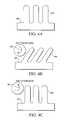
- FIGS. 4A-Care cross-sectional views of polishing pads.
- FIG. 4Ais a view of a new polishing pad.
- FIG. 4Bis a view of a polishing pad after conditioning in a first angular direction.
- FIG. 4Cshows the same polishing pad after conditioning in the opposite angular direction.
- FIG. 5is a flow diagram of the feedback loop used in at least some embodiments of a CMP process optimization.
- FIG. 6is a flow diagram illustrating an example of data collection and generation of a pad wear and conditioning model.
- FIG. 7is a model of polishing pad wear based on FIGS. 3 and 4 used in predicting and optimizing the water removal rate in a CMP process.
- FIG. 8is a model of polishing pad recovery based on FIGS. 3 and 4 used in predicting and optimizing the water removal rate in a CMP process.
- FIG. 9is a model based on FIGS. 5 and 6 for predicting and modifying CMP operating parameters to optimize the wafer process.
- FIG. 10is a side sectional view of a CMP machine for use in at least some embodiments of the present invention.
- FIG. 11is a block diagram of a computer system that includes tool representation and access control for use in at least some embodiments of the invention.
- FIG. 12is an illustration of a floppy disk that may store various portions of the software according to at least some embodiments of the invention.
- Novel methods for feed forward and feed back controls of the CMP process for maximizing the life of the polishing padare described herein.
- Extended pad liferesults in reduced down time for the CMP process because the polishing pad can polish more wafers over a longer period of time without requiring replacement or adjustment (e.g., removal of the damaged portion of the pad).
- waferis used in a general sense to include any substantially planar object that is subject to polishing. Wafers include, in additional to monolith structures, substrates having one or more layers or thin films or other architecture deposited thereon.
- the polishing pad surfaceneeds to maintain a certain level of roughness and elasticity in order to provide the required wafer material removal rates in a CMP process.
- the roughness and elasticity of the paddecreases with successive wafer polishes, thereby reducing the wafer material removal rate.
- Initial polishing pad surface conditionsare shown in FIG. 3A , at which time surface roughness is at a maximum. After the pad has been used for polishing, these asperities are pushed down, often in varying directions. To compensate for this, and restore at least some of the roughness of the pad, the pad is conditioned using, for example, a conditioning disk that rotates, for example, in the direction indicated by arrow 340 shown in FIG. 3 B.
- FIG. 2shows the decrease in removal rate over time as a result of the conditioning process shown in FIGS. 3A-C .
- FIGS. 4A , 4 B and 4 Crepresent a simplified model used for overcoming the aforementioned bias issue, wherein the angular velocity of the conditioning disk is alternated.
- FIG. 4Athis figure shows initial polishing pad surface conditions.
- the polishing pad 400is conditioned by contacting the pad with a conditioning disk at a first angular velocity (e.g., clockwise, indicated by arrow 420 in FIG. 4 B), which introduces some directionality to the polishing pad surface features 440 .
- the angular velocity of the conditioning diskis reversed (e.g., counterclockwise, as shown by arrow 460 in FIG. 4C ) to “undue” the effect of the previous conditioning events.
- Alternating the speed and direction of conditioningextends the surface roughness and elasticity.
- the process shown in FIGS. 4A , 4 B and 4 Cmay be repeated for the entire life cycle of the pad until no more active sites are available.
- the polishing padmay be conditioned in a first direction for a predetermined number of times after which the direction of conditioning is reversed.
- the optimal number of conditioning events in a particular directionis expected to change (decrease) as the pad ages.
- the model for pad conditioning and recoveryadjusts the process accordingly.
- the mechanical processes described above during wafer planarization and conditioning of the polishing padprovide a model for optimization of the planarization process.
- pad conditioning parametersaccording to this model, the pad life can be extended without compromise to the wafer material removal rate.
- speed and direction of the conditioning diskan optionally other operating variables such as conditioning frequency, conditioning duration, and transitional speed of conditioning disk across the pad surface, are adjusted in a feed forward and feed back loop that predicts and then optimizes pad conditioning operating parameters.
- an initial modelis developed based upon knowledge of the wafer polishing process, and is used in at least some embodiments of the present invention as is shown in FIG. 5 .
- initial processing conditionsare identified that will provide a wafer material removal rate between a preselected minimum and maximum value for a given set of conditioning parameters, hereinafter, the “acceptable” range for wafer material removal rates. The conditions are selected to prevent overconditioning of the pad.
- wafersare polished according to the initial conditions in step 500 .
- the thicknesses of the polished wafersare measured and a wafer material removal rate is calculated in step 510 , which information is then used in a feedback loop to maintain the wafer material removal rate within the accepted range.
- the actual removal rateis compared with the predicted removal rate (derived from the pad wear model). Deviations, i.e., prediction errors, are used to adjust pad conditioning parameters in step 520 according to the model of the invention to compensate for the reduced polishing capability of the polishing pad as identified in the model and/or to correct for any un-modeled effects.
- the polishing padis conditioned according to the updated conditioning parameters in step 530 . Polishing is repeated in step 540 and the polishing results are used to further update the polishing conditions by repeating steps 510 - 530 .
- conditioning parametersmay be used that are just sufficient to restore polishing pad effectiveness, but which do not unduly damage the pad.
- Pad conditioning optimizationis carried out with reference to a specific polishing system. That is, the conditions that improve pad lifetime are specific to the type of wafer being polished, the slurry used in polishing and the composition of the polishing pad. Once a wafer/slurry/polishing pad system is identified, the system is characterized using the models developed and discussed herein. Exemplary polishing pad and wafer parameters include polishing pad size, polishing pad composition, slurry composition, wafer composition, rotational velocity of the polishing pad, polishing pad pressure, and translational velocity of the wafer.
- a separate model(or at least a supplement to a composite model) is created for each slurry/polishing pad wafer combination (i.e., for each different type/brand of slurry and each type/brand of pad) that may be used in production with a given type of wafer.
- FIG. 6shows a flow diagram of the steps used in the development of the pad wear and conditioning model in at least some embodiments of the invention.
- DOEdesign of experiment
- a first conditioning parameter x 1e.g., conditioning disk angular velocity (rpm)
- the relationshipis determined by measuring wafer material removal rates at different conditioning disk angular velocities with wafer parameters such as polishing force, polishing duration, etc., held constant.
- wafer parameterssuch as polishing force, polishing duration, etc.
- Pad conditioning and wafer polishingmay be carried out simultaneously, i.e., using an apparatus such as shown in FIG. 10 , or pad conditioning may be followed by wafer polishing.
- the conditioning disk velocityis increased incrementally from wafer to wafer (or thickness measurement to thickness measurement) with all other parameters held constant, and the wafer removal rate is again determined.
- a curve as shown in FIG. 7may be generated, which illustrates the effect of the conditioning disk velocity on the wafer's material removal rate for a given polishing system (all other parameters being held constant).
- the curveis represented as a linear curve over the removal rate of interest, but may, in at least some embodiment of the invention, be a non-linear, e.g. quadratic or exponential curve.
- a curve 700represents the change in wafer material removal rate with time (as determined by number of wafers polished) for a given set of operating parameters.
- the removal rateis represented as decreasing linearly with time until an equilibrium rate is achieved, which may be, but is not required to be, less than the minimum removal rate 770 , which is determined by the operator, for example, based upon production needs.
- the slope of the curveis characterized by the angle ⁇ 1 .
- the curvecan be, in at least some of embodiments, linear or non-linear, e.g. exponential or quadratic, or the like.
- the minimum wafer material removal rateis dictated by production goals, since a minimal wafer throughput rate is needed.
- the maximum wafer material removal rate 795is defined as the initial removal rate.
- Successive curves 720 , 740 , 760may also be generated for different conditioning disk velocities (here increasing velocities are shown).
- the removal rate range 780defines the removal rate maximum and minimum for the model, where the maximum removal rate is the initial removal rate and the minimum removal rate is production determined. Intersection of curves 700 , 720 , 740 , 760 with the minimum removal rate defines the upper limit of wafers that can be polished under the defined pad conditioning parameters.
- the angles ⁇ 1 , ⁇ 2 , ⁇ 3 , and ⁇ 4are defined by the intersection of the equilibrium curve 790 with curves 700 , 720 , 740 , 760 , respectively.
- the values for ⁇are descriptive of the response of the polishing process to conditioning parameters. The larger the value for ⁇ , the steeper the slope of the curve and the more sensitive the planarization process is to conditioning parameters.
- step 620the relationship between wafer material removal rate and a second conditioning parameter, e.g., direction of pad conditioning, is determined in the same polishing system.
- step 630x 2 , maximum and minimum values for the second conditioning parameter and wafer material removal rates is determined.
- Curve 800represents the increase in wafer material removal rate with time (as determined by number of wafers polished) for a given angular velocity as the flattening of the polishing pad surface is alleviated upon conditioning in the reverse direction.
- the removal rateis shown as increasing linearly with time until a saturation point 810 is achieved, which is typically less than the initial maximum removal rate of the pad.
- the curvemay be linear or non-linear, e.g. expotential or quadratic, or the like. Additional polishing results in loss of surface roughness due to orientation in the opposite direction, and so wafer material removal rates again are expected to decline.
- the maximum wafer material removal rate 815is defined at the curve maximum.
- an operating minimum wafer material removal rate 825can be suggested by production goals, since a minimal wafer throughput rate is needed.
- the removal rate range 880defines the removal rate maximum and minimum for the pad recovery model.
- successive curves 820 , 840 , 860are also generated for different velocities of the conditioning disk.
- Each curvereaches a maximum, which represents the optimal recovery of the polishing pad due to reversal of the conditioning direction and then declines.
- the angles ⁇ 1 , ⁇ 2 , ⁇ 3 , and ⁇ 4are defined for each curve 800 , 820 , 840 , 860 , respectively.
- the value for ⁇is descriptive of the recovery of the polishing pad. The larger the value for ⁇ , the steeper the slope of the curve and the more sensitive the recovery process is to conditioning parameters. Since it is not possible to fully compensate for pad wear by reversing direction of conditioning, for a given sample curve conditioned at a given angular velocity, ⁇ > ⁇ .
- the wafer material removal ratewill again decline and approach the minimum acceptable removal rate.
- the direction of the conditioning diskis again reversed and wafer material removal rates are expected to increase once again.
- the values for each successive maximum in the recovery curves of FIG. 8are expected to decrease until performance above the minimum removal rate is not possible.
- the conditioning velocityis increased in order to bring the removal rate into the acceptable range.
- the model at the higher velocityis now used to predict future performance.
- the modelcan be represented as raw data that reflects the system, or it can be represented by equations, for example multiple input-multiple output linear, quadratic and non-linear equations, which describe the relationship among the variables of the system.
- Feedback and feed forward control algorithmsare constructed in step 660 based on the above model using various methods.
- the wafer removal ratemay be defined as the weighted contribution of all the pad conditioning parameters, x 1 through x n .
- the algorithmsmay be used to optimize conditioning parameters using various methods, such as recursive parameter estimation. Recursive parameter estimation is used in situations such as these, where it is desirable to model on line at the same time as the input-output data is received. Recursive parameter estimation is well-suited for making decisions on-line, such as adaptive control or adaptive predictions. For more details about the algorithms and theories of identification, see Ljung L., System Identification—Theory for the User, Prentice Hall, Upper Saddle River, N.J. 2nd edition, 1999.
- the wafer material removal rateis described according to eq. 2:
- R ⁇ ⁇ e ⁇ ⁇ m ⁇ ⁇ o ⁇ ⁇ v ⁇ ⁇ a ⁇ ⁇ l ⁇ ⁇ R ⁇ ⁇ a ⁇ ⁇ ⁇ t ⁇ ⁇ e ] min maxf ( ⁇ d ⁇ ⁇ i ⁇ ⁇ s ⁇ ⁇ k ] min max , f ] min max , t c ⁇ ⁇ o ⁇ n ⁇ d ⁇ ⁇ i ⁇ t ⁇ i ⁇ ⁇ o ⁇ ⁇ n ⁇ i ⁇ ⁇ n ⁇ g ] min max , d ⁇ ⁇ i ⁇ r ⁇ ⁇ e ⁇ ⁇ c ⁇ ⁇ t ⁇ i ⁇ o ⁇ ⁇ ⁇ ⁇
- t conditioningis the duration of conditioning
- fis frequency of conditioning.
- Frequencyis measured as the interval, e.g., number of wafers polished, between conditioning events and direction is defined above. For example, a frequency of 1 means that the pad is conditioned after every wafer, while a frequency of 3 means that the pad is conditioned after every third wafer.
- the sweeping speedis the speed at which the conditioning disk moves across the surface of the polishing pad. The motion is indicated by arrow T 2 in FIG. 10 .
- t (time), T 2 (sweep speed), and f (frequency)are held constant.
- the objective functionis to maintain removal rates within the minimum and maximum allowable rates (the “acceptable rates”) by controlling the conditioning disk speed and direction, and, optionally, by controlling other factors such as frequency and duration of conditioning, conditioning disk down force, speed of translation of the conditioning disk across the pad surface.
- the conditioning parametersis maintained within their determined boundary conditions, i.e., minimum and maximum values, as well.
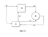
- the CMP parameters (variable) and constants from the modelmay then be programmed into a computer, which may then constantly monitor and appropriately vary the parameters during the process to improve the wafer material removal rate and the pad life, as shown in FIG. 9 .
- Parameters from the base study 901are input into the computer or other controller 902 , which runs the wafer polishing process, and the estimator 903 , which monitors and modifies the process parameters.
- the actual output (i.e., measured removal rate) 904is monitored and compared to the predicted output (i.e., target removal rate) 905 calculated by estimator 903 .
- the difference 906 between the actual output 904 and the predicted output 905is determined and reported 907 to the estimator 903 , which then appropriately generates updated parameters 908 for the process 902 .
- Updating model parameters for feedback controlis based on eq. 3.
- k( k 1 )+ g* ( k ⁇ ( k 1 )), (3) where k is a current parameter, k 1 is a previous parameter estimate, g is the estimate gain and (k ⁇ (k 1 )) is the prediction error.
- Estimate gainis a constant selected by the user, which is used as a measure of machine error or variability. Gain factor may be determined empirically or by using statistical methods. In at least some embodiments, the gain is in the range of about 0.5 to 1.0, or in at least some embodiments, in the range of about 0.7 to 0.9.
- a series of curvesmay be generated for a polishing system of interest as described above for determining the relationship between wafer material removal rate and conditioning disk rotational velocity and direction.
- Curvesare generated using a standard polishing procedure, with all operating conditions held constant with the exception of the parameter(s) under investigation.
- Exemplary polishing pad and wafer parameters that are held constantinclude polishing pad size, polishing pad composition, wafer composition, polishing time, polishing force, rotational velocity of the polishing pad, and rotational velocity of the wafer.
- the variable parametersinclude at least the angular speed and direction of the conditioning disk; however, additional parameters may be included in the model. Using the model such as shown in FIG. 6 for at least some of the embodiments of the invention, and the curves generated as in FIGS.
- values for ⁇ 1 - ⁇ 4 , ⁇ 1 - ⁇ 4 , minimum and maximum values for wafer material removal rate, conditioning down force and conditioning disk rotational velocityare determined.
- An algorithm that models the wafer planarizationis defined, and a first set of pad conditioning parameters may be determined for a polishing system of interest, either empirically or using historical data or data from the DOE.
- An algorithm which models the pad wear and pad recovery processis input into the estimator and a predicted wafer material removal rate is calculated based upon the model. The actual results are compared against the predicted results and the error of prediction is fed back into the estimator to refine the model. New conditioning parameters are then determined. Based upon the models described herein, these parameters are just sufficient to revitalize the pad surface without overconditioning. Thus, the smallest increment in conditioning parameters that meet the model criteria is selected for the updated conditioning parameters. Subsequent evaluation of the updated model will determine how good is the fit, and further modifications can be made, if necessary, until the process is optimized.
- the conditioning parametersare updated in discrete increments or steps, defined by way of example, by the incremental curves shown in FIGS. 7 and 8 .
- a suitable number of curvesare generated so that steps are small enough to permit minor adjustments to the conditioning parameters.
- the updated conditioning parametersmay be determined by interpolation to the appropriate parameters, which may lie between curves. Interpolation may be appropriate in those instances where a fewer number of curves are initially generated and the experimental results do not provide a fine resolution of the parameters.
- deviations from the predicted ratereflects, in part, the inability of the model to account for all factors contributing to the process (this may be improved with subsequent iterations of the feedback process)
- deviations from the predicted wafer material removal rate over timerepresent a degradation in CMP pad polishing.
- gain factormay be used to reflect uncertainty in the measured or calculated parameters, or to “damp” the effect of changing parameters too quickly or to a too great an extent. It is possible, for example, for the model to overcompensate for the prediction error, thereby necessitating another adjustment to react to the overcompensation. This leads to an optimization process that is jumpy and takes several iterations before the optimized conditions are realized. Use of a gain factor in updating the parameters for feedback control qualifies the extent to which the model will react to the prediction error.
- conditioning down forcewhich may be set to a constant value in the initial study, may be increased (or decreased). The system is monitored to determine the effect this change had on the system. It should be readily apparent that other factors relevant to pad wear and conditioning may be evaluated in this manner.
- conditioning timerepetition time of the disk on the pad
- conditioning disk translational speedconditioning down force, and the like
- the modelmay be modified to include additional parameters in the model.
- the apparatushas a conditioning system 1010 including a carrier assembly 1020 , a conditioning disk 1030 attached to the carrier assembly, and a controller 1040 operatively coupled to the carrier assembly to control the down force (F) and rotation rate ( ⁇ ) of the conditioning disk.
- the carrier assemblymay have an arm 1050 to which the conditioning disk 1030 is attached and means 1060 a-d to move the conditioning disk in and out of contact with the planarizing surface.
- the controller 1040may be operatively coupled to the moving means to adjust the height and position of the arm carrying the conditioning disk ( 1060 a , 1060 b , 1060 c , 1060 d ). Similar controls for control of the position and movement of the wafer may also be present.
- the controlleradjusts the operating parameters of the conditioning disk, e.g., down force and rotation rate, in response to changes in wafer material removal rate.
- the controllermay be computer controlled to automatically provide conditioning according to the calculated conditioning recipe.
- the apparatusprovides a means for selectively varying the pad conditioning parameters over the operating life of the pad 1080 in order to extend pad life without compromise to the planarization process of the wafer 1090 .
- Other types of deviceswhere, e.g., other components have their height, positions, and/or rotations adjusted are also contemplated by at least some embodiments of the present invention.
- Additional apparatus utilized to implement the feedforward and feedback loopinclude a film thickness measurement tool to provide thickness data needed to calculate wafer material removal rate.
- the toolmay be positioned on the polishing apparatus so as to provide in-line, in situ measurements, or it may be located remote from the polishing apparatus.
- the toolmay use optical, electrical, acoustic or mechanical measurement methods.
- a suitable thickness measurement deviceis available from Nanometrics (Milpitas, Calif.) or Nova Measuring Instruments (Phoenix, Ariz.).
- a computermay be utilized to calculate the optimal pad conditioning recipe based upon the measured film thickness and calculated removal rate, employing the models and algorithm provided according to the invention.
- a suitable integrated controller and polishing apparatus(Mirra with iAPC or Mirra Mesa with iAPC) is available from Applied Materials, California.
- Exemplary semiconductor wafersthat can be polished using the concepts discussed herein including, but are not limited to those made of silicon, tungsten, aluminum, copper, BPSG, USG, thermal oxide, silicon-related films, and low k dielectrics and mixtures thereof.
- CMP polishing padsthere are numerous CMP polishing pads in the art which are generally made of urethane or other polymers. However, any pad that can be reconditioned can be evaluated and optimized using the method of the invention. Exemplary polishing pads include EpicTM polishing pads (Cabot Microelectronics Corporation, Aurora Ill.) and Rodel® IC1000, IC1010, IC1400 polishing pads (Rodel Corporation, Newark, Del.), OXP series polishing pads (Sycamore Pad), Thomas West Pad 711, 813, 815, 815-Ultra, 817, 826, 828, 828-E1 (Thomas West).
- EpicTM polishing padsCabot Microelectronics Corporation, Aurora Ill.
- Rodel® IC1000, IC1010, IC1400 polishing padsRodel Corporation, Newark, Del.
- OXP series polishing padsSycamore Pad
- any number of different types of slurrycan be used in the methods of the invention.
- CMP polishing slurriesin the art, which are generally made to polish specific types of metals in semiconductor wafers.
- Exemplary slurriesinclude Semi-Sperse® (available as Semi-Sperse® 12, Semi-Sperse® 25, Semi-Sperse® D7000, Semi-Sperse® D7100, Semi-Sperse® D7300, Semi-Sperse® P1000, Semi-Sperse® W2000, and Semi-Sperse® W2585) (Cabot Microelectronics Corporation, Aurora Ill.), Rodel ILD1300, Klebesol series, Elexsol, MSW1500, MSW2000 series, CUS series and PTS (Rodel).
- the method of the inventioncan be used to predict pad life for tool scheduling. For example, if the number of wafers, after each condition cycle decreases, one could predict a pad life end point and use that prediction to schedule retooling.
- the methodologycan also be used together with an optimization engine when the wafer polishing parameters are changing through an optimization engine.
- pad conditioning optimizationmay be carried out together with optimization of wafer polishing. This can be accomplished through optimization by having the optimization search engine's objective function minimize a function that describes both polishing and conditioning parameters.
- the optimization processthen seeks to minimize S.
- the method of the present inventioncan be used under conditions when the polishing parameters are held constant or when the polishing parameters are to be changed through optimization.
- a bus 1156serves as the main information highway interconnecting the other components of system 1111 .
- CPU 1158is the central processing unit of the system, performing calculations and logic operations required to execute the processes of embodiments of the present invention as well as other programs.
- Read only memory (ROM) 1160 and random access memory (RAM) 1162constitute the main memory of the system.
- Disk controller 1164interfaces one or more disk drives to the system bus 1156 . These disk drives are, for example, floppy disk drives 1170 , or CD ROM or DVD (digital video disks) drives 1166 , or internal or external hard drives 1168 . These various disk drives and disk controllers are optional devices.
- a display interface 1172interfaces display 1148 and permits information from the bus 1156 to be displayed on display 1148 .
- Display 1148can be used in displaying a graphical user interface.
- Communications with external devices such as the other components of the system described abovecan occur utilizing, for example, communication port 1174 .
- Optical fibers and/or electrical cables and/or conductors and/or optical communicatione.g., infrared, and the like
- wireless communicatione.g., radio frequency (RF), and the like
- Peripheral interface 1154interfaces the keyboard 1150 and mouse 1152 , permitting input data to be transmitted to bus 1156 .
- system 1111also optionally includes an infrared transmitter and/or infrared receiver.
- Infrared transmittersare optionally utilized when the computer system is used in conjunction with one or more of the processing components/stations that transmits/receives data via infrared signal transmission.
- the computer systemmay also optionally use a low power radio transmitter 1180 and/or a low power radio receiver 1182 .
- the low power radio transmittertransmits the signal for reception by components of the production process, and receives signals from the components via the low power radio receiver.
- the low power radio transmitter and/or receiverare standard devices in industry.
- system 1111 in FIG. 11is illustrated having a single processor, a single hard disk drive and a single local memory, system 1111 is optionally suitably equipped with any multitude or combination of processors or storage devices.
- system 1111may be replaced by, or combined with, any suitable processing system operative in accordance with the principles of embodiments of the present invention, including sophisticated calculators, and hand-held, laptop/notebook, mini, mainframe and super computers, as well as processing system network combinations of the same.
- FIG. 12is an illustration of an exemplary computer readable memory medium 1284 utilizable for storing computer readable code or instructions.
- medium 1284may be used with disk drives illustrated in FIG. 11 .
- memory mediasuch as floppy disks, or a CD ROM, or a digital video disk will contain, for example, a multi-byte locale for a single byte language and the program information for controlling the above system to enable the computer to perform the functions described herein.
- ROM 1160 and/or RAM 1162 illustrated in FIG. 11can also be used to store the program information that is used to instruct the central processing unit 1158 to perform the operations associated with the instant processes.
- suitable computer readable media for storing informationinclude magnetic, electronic, or optical (including holographic) storage, some combination thereof, etc.
- the mediumcan be in the form of a transmission (e.g., digital or propagated signals).
Landscapes
- Engineering & Computer Science (AREA)
- Mechanical Engineering (AREA)
- Physics & Mathematics (AREA)
- General Physics & Mathematics (AREA)
- Manufacturing & Machinery (AREA)
- Automation & Control Theory (AREA)
- Power Engineering (AREA)
- Microelectronics & Electronic Packaging (AREA)
- Computer Hardware Design (AREA)
- Condensed Matter Physics & Semiconductors (AREA)
- General Engineering & Computer Science (AREA)
- Quality & Reliability (AREA)
- Human Computer Interaction (AREA)
- Mechanical Treatment Of Semiconductor (AREA)
- Finish Polishing, Edge Sharpening, And Grinding By Specific Grinding Devices (AREA)
- Grinding-Machine Dressing And Accessory Apparatuses (AREA)
Abstract
Description
This application claims priority under 35 U.S.C. §119(e) from now abandoned application Ser. No. 60/298,878 filed Jun. 19, 2001 and entitled “Advanced Process Control for Semiconductor Manufacturing Process.”
This application claims priority under 35 U.S.C. §119(e) from now abandoned application Ser. No. 60/305,798, filed Jul. 16, 2001 and entitled “Feedforward and Feedback Control for Conditioning of Chemical Mechanical Polishing Pad.”
This application claims priority under 35 U.S.C. §119(e) from now abandoned application Ser. No. 60/318,743, filed Sep. 12, 2001 and entitled “Feedforward and Feedback Control for Conditioning of Chemical Mechanical Polishing Pad.”
The present invention is generally directed to the area of polishing and methods for improving the life and effectiveness of polishing pads in a chemical mechanical polishing process.
Chemical-mechanical polishing (CMP) is used in semiconductor fabrication processes for obtaining full planarization of a semiconductor wafer. The method involves removing material (e.g., a sacrificial layer of surface material) from the wafer, (typically silicon dioxide (SiO2)) using mechanical contact and chemical erosion from, e.g., a moving polishing pad saturated with slurry. Polishing flattens out height differences, since areas of high topography (hills) are removed faster than areas of low topography (valleys).FIG. 1A shows a top view of aCMP machine 100, andFIG. 1B shows a side section view of theCMP machine 100 taken through line AA. TheCMP machine 100 is fed wafers to be polished. Typically, theCMP machine 100 picks up awafer 105 with anarm 101 and places it onto a rotatingpolishing pad 102. Thepolishing pad 102 is made of a resilient material and is often textured, to aid the polishing process Thepolishing pad 102 rotates on aplaten 104 or turn table located beneath thepolishing pad 102 at a predetermined speed. Thewafer 105 is held in place on thepolishing pad 102 by thearm 101. The lower surface of thewafer 105 rests against thepolishing pad 102. The upper surface of thewafer 105 is against the lower surface of thewafer carrier 106 ofarm 101. As thepolishing pad 102 rotates, thearm 101 rotates thewafer 105 at a predetermined rate. Thearm 101 forces thewafer 105 against thepolishing pad 102 with a predetermined amount of down force. TheCMP machine 100 also includes aslurry dispense arm 107 extending across the radius of thepolishing pad 102. Theslurry dispense arm 107 dispenses a flow of slurry onto thepolishing pad 102.
Over time the polishing pad loses its roughness and elasticity, and thus, its ability to maintain desired removal rates (polishing rates). It is known that the material removal rate provided by a given polishing pad decreases exponentially with time in the manner shown in FIG.2. Further the decreased removal rate requires ever-increasing conditioning parameters, e.g., down force and/or conditioning angular velocity and/or conditioning time, in order to restore the desired removal rate of material from the wafer. As a consequence, the polishing pad must be conditioned (e.g., using a conditioning disk108), between polishing cycles. The conditioning disk is held in place on the polishing pad byarm 109. As the polishing pad rotates, theconditioning disk 108 also rotates. Doing so roughens the surface of the pad and restores, at least temporarily, its original material removal rate. Furthermore, excessive pad conditioning shortens pad life.
A problem with conventional conditioning methods is that they may over-condition, e.g., wear out prematurely, the polishing pad. Each time a pad is replaced, one to several wafers must be polished thereon and the results measured, to ensure that the tool will yield the required polishing. This translates into processing delays and lost tool efficiency.
In an attempt to extend the life of the pad, one may selectively condition portions a polishing pad, or vary the down force of the conditioning element (e.g., conditioning disk108) along the surface of the CMP pad, based upon the distribution of waste matter across the planarizing surface. Other methods of extending pad life include varying the conditioning recipe across the surface of the polishing pad in response to polishing pad non-uniformities. However, these reported CMP processes are typically more concerned with improving the CMP process, e.g., improving within water non-uniformity, than in extending pad life.
Methods and devices that would extend pad life and therefore reduce the frequency of pad replacement offer significant cost savings to the wafer fabrication process.
The present invention relates to a method, system and medium for conditioning a planarizing surface of a polishing pad in order to extend the working life of the pad. More specifically, at least some embodiments of the present invention use physical and/or chemical models (which can be implemented as a single model or multiple models) of the pad wear and wafer planarization processes to predict polishing pad performance and to extend pad life. This results in an increase in the number of semiconductor wafer or other substrates that can be polished with a single polishing pad, thereby providing significant cost savings in the CMP process, both in extending pad life and reducing the time devoted to pad replacement.
The model predicts polishing effectiveness (wafer material removal rate) based on the “conditioning” operating parameters of the conditioning process. In at least some embodiments of the present invention, operating parameters of conditioning include angular direction and angular velocity of a conditioning disk (where a disk is used to condition) during conditioning, and may also include other factors, such as the frequency of conditioning and time of conditioning. The model selects, and then maintains, polishing pad conditioning parameters within a range that does not overcondition the pad while providing acceptable wafer material removal rates. Thus the present invention provides a process for the feed forward and feed backward control of the CMP polishing process.
In one aspect of the invention, a method of conditioning a planarizing surface in a CMP apparatus having a polishing pad and a conditioning disk includes polishing a wafer in the CMP apparatus under a first set of pad conditioning parameters selected to maintain wafer material removal rates within preselected minimum and maximum removal rates; measuring a wafer material removal rate occurring during said polishing step; calculating, based upon said wafer material removal rate, updated pad conditioning parameters to maintain wafer material removal rates within the maximum and minimum removal rates; and conditioning the polishing pad using the updated pad conditioning parameters. The updated pad conditioning parameters are calculated using a pad wear and pad recovery model by calculating wafer material removal rate as a function of pad conditioning parameters including conditioning disk rotational speed and direction; and determining the difference between the calculated and measured wafer material removal rates and calculating updated pad conditioning parameters to reduce said difference, wherein the updated conditioning parameters are updated according to the equation k=(k1)+g*(k−(k1)), where k is a measured parameter, k1is calculated parameter estimate, g is the estimate gain and (k−(k1)) is the prediction error.
In at least some embodiments of the invention, the first set of pad conditioning parameters are determined empirically, or using historical data, or using the results of the design of experiment (DOE).
In at least some embodiments of the invention, the pad conditioning parameters of the pad wear and pad recovery model further includes frequency of conditioning, or time of conditioning, or translational speed of conditioning disk during conditioning.
In at least some embodiments of the invention, the step of determining the wafer material removal rate includes measuring the wafer thickness before and after polishing.
In at least some embodiments of the invention, the step of calculating updated pad conditioning parameters in step (c) includes executing a recursive optimization process, or in at least some embodiments, includes calculating conditioning parameters such that the parameter is within determined maximum and minimum values.
In at least some embodiments of the present invention, the gain is an indication of variability or reliability in the measured parameter, and the gain is in the range of about 0.5 to 1.0, or gain is in the range of about 0.7 to 0.9.
In at least some embodiments, updated pad conditioning parameters are calculated by determining a difference between an output of the pad wear and pad conditioning model and the wafer material removal step (c). In at least some embodiments, this difference is minimized.
In at least some embodiments of the invention, the steps (b) through (e) are repeated.
In at least some embodiments of the invention, the maximum value for wafer material removal rate is the saturation point of the wafer material removal rate vs. conditioning down force curve, or in at least some embodiments, the maximum value for wafer material removal rate is the initial rate, or in at least some embodiments, the minimum value for wafer material removal rate is defined by the maximum acceptable wafer polishing time.
In at least some embodiments of the invention, the wafer material removal rate is defined by the equation
where ωdiskis the angular velocity of the conditioning disk during conditioning of the polishing pad, t is the time of conditioning, f is the frequency of condition, direction is the spinning direction of the conditioning disk, and T2is the sweeping speed of the conditioning disk during conditioning.
In another aspect of the invention, an apparatus for conditioning polishing pads used to planarize substrates includes a carrier assembly having an arm positionable over a planarizing surface of a polishing pad; a conditioning disk attached to the carrier assembly; and an actuator capable of controlling an operating parameter of the conditioning disk; and a controller operatively coupled to the actuator, the controller operating the actuator to adjust the operating parameter of the conditioning disk as a function of a pad wear and pad recovery model that predicts the wafer material removal rate based upon conditioning pad rotational speed and direction.
In at least some embodiments of the invention, the updated pad conditioning parameters are calculated using a pad wear and pad recovery model by calculating wafer material removal rate as a function of pad conditioning parameters including conditioning disk rotational speed and direction; and determining the difference between the calculated and measured wafer material removal rates and calculating updated pad conditioning parameters to reduce said difference, wherein the updated conditioning parameters are updated according to the equation k=(k1)+g*(k−(k1)), where k is a measured parameter, k1is calculated parameter estimate, g is the estimate gain and (k−(k1)) is the prediction error.
In at least some embodiments, the pad conditioning parameters of the pad wear and pad recovery model further includes frequency of conditioning, time of conditioning, or speed of conditioning disk during conditioning.
In at least some other embodiments of the present invention, the gain is an indication of variability or reliability in the measured parameter.
In another aspect of the invention, a method of developing a pad wear and pad conditioning model for optimization of the pad conditioning for polishing pads used to remove material from a wafer, is provided. The method includes:
a) determining the relationship between at least one pad conditioning parameter and wafer material removal rate;
b) determining maximum and minimum values for each of the at least one pad conditioning parameters and the wafer material removal rate; and
c) recording the relationships and minimum and maximum values of the at least one pad conditioning parameter and the wafer removal rate.
In at least some embodiments of the invention, the at least one pad conditioning parameter includes a plurality of parameters and the wafer removal rate is defined as a weighted function of the plurality of pad conditioning parameters, or in at least some embodiments, the at least one pad conditioning parameters includes conditioning disk rotational speed, or in at least one embodiment, the at least one pad conditioning parameter further includes conditioning disk rotational direction.
In at least some embodiments of the invention, the at least one pad conditioning parameter includes one or more parameters selected from the group consisting of conditioning disk down force, conditioning disk rotational rate and direction, frequency and duration of conditioning, and conditioning disk translational speed.
In at least some embodiments of the invention, the relationship between the at least one conditioning parameter and wafer removal rate is determined by incrementally varying the conditioning parameter and measuring the resultant wafer removal rate.
In at least some embodiments of the invention, the maximum value for the conditioning parameter is the value above which no incremental increase of the wafer removal rate is observed, or in at least some embodiments, the minimum value for the conditioning parameter is the value which provides the minimum wafer removal rate.
In at least some embodiments of the invention, the invention further includes polishing a wafer in the CMP apparatus under a first set of pad conditioning parameters selected to maintain wafer material removal rates within preselected minimum and maximum removal rates including conditioning disk rotational speed and direction, determining a wafer material removal rate occurring during said polishing step, calculating updated pad conditioning parameters based upon said determined wafer material removal rate and the pad wear and conditioning model to maintain wafer material removal rates within the maximum and minimum removal rates, and conditioning the polishing pad using the updated pad conditioning parameters.
In at least some embodiments of the invention, the updated pad conditioning parameters are calculated by determining the difference between an output of the pad wear and conditioning model and said determined wafer material removal, or in at least some embodiments, the updated pad conditioning parameters are updated according to the equation k=(k,1)+g*(k−(k1)), where k is a measured wafer material removal rate, k1is a calculated wafer material removal rate, g is the estimate gain, and (k−(k1)) is the prediction error.
In another aspect of the invention, a computer readable medium is provided having instructions being executed by a computer, the instructions including a computer-implemented software application for a chemical mechanical polishing process. The instructions for implementing the process include:
a) receiving data from a chemical mechanical polishing tool relating to the wafer removal rate of at least one wafer processed in the chemical mechanical polishing process; and
b) calculating, from the data of step (a), updated pad conditioning parameters within defined maximum and minimum values, wherein the updated pad conditioning parameters are calculated by determining the difference between an output of a pad wear and conditioning model and the data of step (a).
In at least some embodiments of the invention, calculating updated conditioning parameters includes calculating parameters such that the parameter is within the determined minimum and maximum values, or in at least some embodiments, calculating updated pad conditioning parameters in step (b) comprises executing a recursive optimization process.
In at least some embodiments of the invention, the maximum value for wafer material removal rate is the saturation point of the wafer material removal rate vs. conditioning down force curve, or in at least some embodiments, the maximum value for wafer material removal rate is the initial rate, or in at least some embodiments, the minimum value for wafer material removal rate is defined by the minimum acceptable wafer polishing time.
In at least some embodiments of the invention, the difference is adjusted using an estimate gain prior to calculating updated pad conditioning parameters.
In another aspect of the invention, a method of conditioning a planarizing surface in a chemical mechanical polishing (CMP) apparatus having a polishing pad against which a wafer is positioned for removal of material therefrom and a conditioning disk is positioned for conditioning of the polishing pad is provided. The method includes:
(a) developing a pad wear and pad conditioning model that defines wafer material removal rate as a function of pad conditioning parameters by:
- (i) determining the relationship between at least one pad conditioning parameter and wafer material removal rate;
- (ii) determining maximum and minimum values for each of the at least one pad conditioning parameters and the wafer material removal rate;
- (iii) recording the relationships and minimum and maximum values of the at least one pad conditioning parameter and the wafer removal rate;
(b) polishing a wafer in the CMP apparatus under a first set of pad conditioning parameters including conditioning disk rotational speed and direction, selected to maintain wafer material removal rates within preselected minimum and maximum removal rates;
(c) determining a wafer material removal rate occurring during said polishing step;
(d) calculating updated pad conditioning parameters based upon said determined wafer material removal rate of said step (b) and the pad wear and conditioning model to maintain wafer material removal rates within the maximum and minimum removal rates, and
(f) conditioning the polishing pad using the updated conditioning parameters.
In another aspect of the invention, a system for conditioning a planarizing surface in a chemical mechanical polishing (CMP) apparatus having a polishing pad against which a wafer is positioned for removal of material therefrom and a conditioning disk is positioned for conditioning of the polishing pad includes:
a) a pad wear and conditioning model that defines wafer material removal rate as a function of at least one pad conditioning parameters including rotation and direction of the conditioning disk;
b) polishing means for polishing a wafer in the CMP apparatus
c) measuring means for determining a wafer material removal rate; and
d) calculating means for updating pad conditioning parameters based upon a wafer material removal rate measured using means of step (c) and the pad wear and conditioning model to maintain wafer material removal rates within the maximum and minimum removal rates.
Thus, polishing pad life is extended by using an appropriate conditioning angular velocity to keep within the acceptable range of wafer material removal rate and reversing direction of conditioning and/or adjusting angular velocity or other conditioning parameters whenever the removal rate drops below the acceptable removal rate. By applying a “one size fits all” approach to pad conditioning parameters, e.g., by determining conditioning parameters without accounting for actual change in wafer material removal rates, conventional processes overcompensate, thereby removing more pad material than is necessary and accelerating pad wear. In contrast, the present invention thus provides improved conditioning parameters by determining only those forces that are minimally necessary to recondition the damaged pad.
Various objects, features, and advantages of the present invention can be more fully appreciated with reference to the following detailed description of the invention when considered in connection with the following drawings.
Novel methods for feed forward and feed back controls of the CMP process for maximizing the life of the polishing pad are described herein. Extended pad life results in reduced down time for the CMP process because the polishing pad can polish more wafers over a longer period of time without requiring replacement or adjustment (e.g., removal of the damaged portion of the pad). The term wafer is used in a general sense to include any substantially planar object that is subject to polishing. Wafers include, in additional to monolith structures, substrates having one or more layers or thin films or other architecture deposited thereon.
The polishing pad surface needs to maintain a certain level of roughness and elasticity in order to provide the required wafer material removal rates in a CMP process. The roughness and elasticity of the pad decreases with successive wafer polishes, thereby reducing the wafer material removal rate. Initial polishing pad surface conditions (asperities320) are shown inFIG. 3A , at which time surface roughness is at a maximum. After the pad has been used for polishing, these asperities are pushed down, often in varying directions. To compensate for this, and restore at least some of the roughness of the pad, the pad is conditioned using, for example, a conditioning disk that rotates, for example, in the direction indicated byarrow 340 shown in FIG.3B. Although the invention is described herein with disk style conditioners, the use of other conditioning mechanisms is specifically contemplated. This, however, introduces a directional bias into the pad surface features320. Subsequent conditioning operations using the same direction of conditioning may lead to increased directionality in pad surface apserities, thereby blocking the flow of the slurry in the pad and also reducing the contact surface between the pad asperities and the polishing wafer. This is shown by the even greater directional bias of theasperities 320 of FIG.3C. As a result, wafer material removal rates worsen as directional bias of the pad surface features increases.FIG. 2 shows the decrease in removal rate over time as a result of the conditioning process shown inFIGS. 3A-C .
Thus, the polishing pad may be conditioned in a first direction for a predetermined number of times after which the direction of conditioning is reversed. The optimal number of conditioning events in a particular direction is expected to change (decrease) as the pad ages. The model for pad conditioning and recovery adjusts the process accordingly.
The mechanical processes described above during wafer planarization and conditioning of the polishing pad provide a model for optimization of the planarization process. By adjusting pad conditioning parameters according to this model, the pad life can be extended without compromise to the wafer material removal rate. In particular, speed and direction of the conditioning disk, an optionally other operating variables such as conditioning frequency, conditioning duration, and transitional speed of conditioning disk across the pad surface, are adjusted in a feed forward and feed back loop that predicts and then optimizes pad conditioning operating parameters.
According to at least one embodiment of the present invention, an initial model is developed based upon knowledge of the wafer polishing process, and is used in at least some embodiments of the present invention as is shown in FIG.5. Based on that initial model, e.g., the wafer and polishing pad parameters remain constant, initial processing conditions are identified that will provide a wafer material removal rate between a preselected minimum and maximum value for a given set of conditioning parameters, hereinafter, the “acceptable” range for wafer material removal rates. The conditions are selected to prevent overconditioning of the pad.
Referring now toFIG. 5 , wafers are polished according to the initial conditions instep 500. The thicknesses of the polished wafers are measured and a wafer material removal rate is calculated instep 510, which information is then used in a feedback loop to maintain the wafer material removal rate within the accepted range. The actual removal rate is compared with the predicted removal rate (derived from the pad wear model). Deviations, i.e., prediction errors, are used to adjust pad conditioning parameters instep 520 according to the model of the invention to compensate for the reduced polishing capability of the polishing pad as identified in the model and/or to correct for any un-modeled effects. The polishing pad is conditioned according to the updated conditioning parameters instep 530. Polishing is repeated instep 540 and the polishing results are used to further update the polishing conditions by repeating steps510-530.
By maintaining the wafer material removal rate and conditioning parameters within the preselected minimum and maximum range, overconditioning of the pad is prevented; that is, conditioning parameters may be used that are just sufficient to restore polishing pad effectiveness, but which do not unduly damage the pad. In operation, it may be desirable to select pad conditioning parameters that result in wafer material removal rates that are close to the minimum acceptable rates, as these conditioning forces are less aggressive and therefore are more likely to avoid overconditioning of the polishing pad. However, one should be cautious (or at least cognizant) about operating too closely to the minimum removal rate since a sudden degradation in the pad condition may cause the wafer material removal rate to drop below the minimum acceptable rate.
Pad conditioning optimization is carried out with reference to a specific polishing system. That is, the conditions that improve pad lifetime are specific to the type of wafer being polished, the slurry used in polishing and the composition of the polishing pad. Once a wafer/slurry/polishing pad system is identified, the system is characterized using the models developed and discussed herein. Exemplary polishing pad and wafer parameters include polishing pad size, polishing pad composition, slurry composition, wafer composition, rotational velocity of the polishing pad, polishing pad pressure, and translational velocity of the wafer.
In at least some embodiments of the present invention, it is envisioned that a separate model (or at least a supplement to a composite model) is created for each slurry/polishing pad wafer combination (i.e., for each different type/brand of slurry and each type/brand of pad) that may be used in production with a given type of wafer.
Instep 610 ofFIG. 6 , as contemplated by at least some of the embodiments of the invention, minimum and maximum values for the conditioning parameter are determined. With reference toFIG. 7 , acurve 700 represents the change in wafer material removal rate with time (as determined by number of wafers polished) for a given set of operating parameters. The removal rate is represented as decreasing linearly with time until an equilibrium rate is achieved, which may be, but is not required to be, less than theminimum removal rate 770, which is determined by the operator, for example, based upon production needs. The slope of the curve is characterized by the angle θ1. The curve can be, in at least some of embodiments, linear or non-linear, e.g. exponential or quadratic, or the like. The minimum wafer material removal rate is dictated by production goals, since a minimal wafer throughput rate is needed. The maximum wafermaterial removal rate 795 is defined as the initial removal rate.
Instep 620, as contemplated by at least some embodiments of the present invention, the relationship between wafer material removal rate and a second conditioning parameter, e.g., direction of pad conditioning, is determined in the same polishing system. Instep 630, x2, maximum and minimum values for the second conditioning parameter and wafer material removal rates is determined.
As is described above with reference toFIGS. 3 and 4 , once the equilibrium wafer material removal rate or the minimum acceptable material removal rate is reached, recovery is possible by reversing the direction of pad conditioning (see, FIG.4C). With reference toFIG. 8 , a curve is generated to illustrate the effect of direction of conditioning pad rotation on wafer removal rate (all other variables held constant).Curve 800 represents the increase in wafer material removal rate with time (as determined by number of wafers polished) for a given angular velocity as the flattening of the polishing pad surface is alleviated upon conditioning in the reverse direction. The removal rate is shown as increasing linearly with time until asaturation point 810 is achieved, which is typically less than the initial maximum removal rate of the pad. In at least some embodiments of the invention, the curve may be linear or non-linear, e.g. expotential or quadratic, or the like. Additional polishing results in loss of surface roughness due to orientation in the opposite direction, and so wafer material removal rates again are expected to decline. Thus, the maximum wafermaterial removal rate 815 is defined at the curve maximum. As above, an operating minimum wafermaterial removal rate 825 can be suggested by production goals, since a minimal wafer throughput rate is needed. Theremoval rate range 880 defines the removal rate maximum and minimum for the pad recovery model.
In at least some embodiments of the invention,successive curves curve
According to the above model, once the maximal recovery in wafer material removal rates is achieved, the wafer material removal rate will again decline and approach the minimum acceptable removal rate. The direction of the conditioning disk is again reversed and wafer material removal rates are expected to increase once again. The values for each successive maximum in the recovery curves ofFIG. 8 are expected to decrease until performance above the minimum removal rate is not possible. At this point, the conditioning velocity is increased in order to bring the removal rate into the acceptable range. The model at the higher velocity is now used to predict future performance.
The results of these studies provide maximum and minimum wafer material removal rates, and performance at different conditioning velocities. In addition, values for constants θ1-θ4and Φ1-Φ4relating to curve slopes may be determined. Although the above designs of experiment show a conditioning parameter that demonstrates an increase in wafer removal rate with increase in magnitude of the parameter, it is understood that the opposite relationship can exist, so that the minimal parameter value produces the maximum wafer removal rate. The models can be adjusted accordingly. Maximum and minimum conditions may be determined for any combination of polishing pad, wafer and polishing slurry known in the art. Additional parameters, up to xn, may be included in the model and their minimum and maximum values determined as indicated bysteps
The model can be represented as raw data that reflects the system, or it can be represented by equations, for example multiple input-multiple output linear, quadratic and non-linear equations, which describe the relationship among the variables of the system. Feedback and feed forward control algorithms are constructed instep 660 based on the above model using various methods. For example, the wafer removal rate may be defined as the weighted contribution of all the pad conditioning parameters, x1through xn. The algorithms may be used to optimize conditioning parameters using various methods, such as recursive parameter estimation. Recursive parameter estimation is used in situations such as these, where it is desirable to model on line at the same time as the input-output data is received. Recursive parameter estimation is well-suited for making decisions on-line, such as adaptive control or adaptive predictions. For more details about the algorithms and theories of identification, see Ljung L.,System Identification—Theory for the User, Prentice Hall,Upper Saddle River, N.J. 2nd edition, 1999.
In at least some embodiments of the present invention, the CMP pad life is a function of surface roughness and pad elasticity as shown in eq. 1:
PadLife=f(surface roughness, elasticity). (1)
PadLife=f(surface roughness, elasticity). (1)
In at least some embodiments of the present invention, the wafer material removal rate is described according to eq. 2:
where ωdiskis the angular velocity (rotational speed, e.g., rpm) of the conditioning disk during conditioning of the polishing pad, direction is the direction of spin, i.e., clockwise or counterclockwise, of the conditioning disk, T2is the translational speed of the conditioning disk across the pad surface, as shown in the exemplary CMP device inFIG. 10 (which will be described in greater detail below), tconditioningis the duration of conditioning, and f is frequency of conditioning. Frequency is measured as the interval, e.g., number of wafers polished, between conditioning events and direction is defined above. For example, a frequency of 1 means that the pad is conditioned after every wafer, while a frequency of 3 means that the pad is conditioned after every third wafer. The sweeping speed is the speed at which the conditioning disk moves across the surface of the polishing pad. The motion is indicated by arrow T2in FIG.10. For the purposes of initial investigation, it is assumed in at least some embodiments of the present invention that t (time), T2(sweep speed), and f (frequency) are held constant.
where ωdiskis the angular velocity (rotational speed, e.g., rpm) of the conditioning disk during conditioning of the polishing pad, direction is the direction of spin, i.e., clockwise or counterclockwise, of the conditioning disk, T2is the translational speed of the conditioning disk across the pad surface, as shown in the exemplary CMP device in
The objective function is to maintain removal rates within the minimum and maximum allowable rates (the “acceptable rates”) by controlling the conditioning disk speed and direction, and, optionally, by controlling other factors such as frequency and duration of conditioning, conditioning disk down force, speed of translation of the conditioning disk across the pad surface. Each of the conditioning parameters is maintained within their determined boundary conditions, i.e., minimum and maximum values, as well.
The CMP parameters (variable) and constants from the model may then be programmed into a computer, which may then constantly monitor and appropriately vary the parameters during the process to improve the wafer material removal rate and the pad life, as shown in FIG.9. Parameters from thebase study 901 are input into the computer orother controller 902, which runs the wafer polishing process, and theestimator 903, which monitors and modifies the process parameters. The actual output (i.e., measured removal rate)904 is monitored and compared to the predicted output (i.e., target removal rate)905 calculated byestimator 903. Thedifference 906 between theactual output 904 and the predictedoutput 905 is determined and reported907 to theestimator 903, which then appropriately generates updatedparameters 908 for theprocess 902.
Updating model parameters for feedback control is based on eq. 3.
k=(k1)+g*(k−(k1)), (3)
where k is a current parameter, k1is a previous parameter estimate, g is the estimate gain and (k−(k1)) is the prediction error. Estimate gain is a constant selected by the user, which is used as a measure of machine error or variability. Gain factor may be determined empirically or by using statistical methods. In at least some embodiments, the gain is in the range of about 0.5 to 1.0, or in at least some embodiments, in the range of about 0.7 to 0.9.
By way of example, a series of curves may be generated for a polishing system of interest as described above for determining the relationship between wafer material removal rate and conditioning disk rotational velocity and direction. Curves are generated using a standard polishing procedure, with all operating conditions held constant with the exception of the parameter(s) under investigation. Exemplary polishing pad and wafer parameters that are held constant include polishing pad size, polishing pad composition, wafer composition, polishing time, polishing force, rotational velocity of the polishing pad, and rotational velocity of the wafer. The variable parameters include at least the angular speed and direction of the conditioning disk; however, additional parameters may be included in the model. Using the model such as shown inFIG. 6 for at least some of the embodiments of the invention, and the curves generated as inFIGS. 7 and 8 , values for θ1-θ4, Φ1-Φ4, minimum and maximum values for wafer material removal rate, conditioning down force and conditioning disk rotational velocity are determined. An algorithm that models the wafer planarization is defined, and a first set of pad conditioning parameters may be determined for a polishing system of interest, either empirically or using historical data or data from the DOE.
An algorithm which models the pad wear and pad recovery process is input into the estimator and a predicted wafer material removal rate is calculated based upon the model. The actual results are compared against the predicted results and the error of prediction is fed back into the estimator to refine the model. New conditioning parameters are then determined. Based upon the models described herein, these parameters are just sufficient to revitalize the pad surface without overconditioning. Thus, the smallest increment in conditioning parameters that meet the model criteria is selected for the updated conditioning parameters. Subsequent evaluation of the updated model will determine how good is the fit, and further modifications can be made, if necessary, until the process is optimized.
In at least some embodiments of the present invention, the conditioning parameters are updated in discrete increments or steps, defined by way of example, by the incremental curves shown inFIGS. 7 and 8 . A suitable number of curves are generated so that steps are small enough to permit minor adjustments to the conditioning parameters.
Also, in at least some embodiments of the present invention, the updated conditioning parameters may be determined by interpolation to the appropriate parameters, which may lie between curves. Interpolation may be appropriate in those instances where a fewer number of curves are initially generated and the experimental results do not provide a fine resolution of the parameters.
While deviations from the predicted rate reflects, in part, the inability of the model to account for all factors contributing to the process (this may be improved with subsequent iterations of the feedback process), deviations from the predicted wafer material removal rate over time represent a degradation in CMP pad polishing. By identifying and modifying the pad conditioning process to account for these changes in polishing capabilities, optimal wafer material removal rates are maintained without overconditioning of the condition pads, e.g., operating above the saturation point of the system.
An additional feature of the method is the use of gain factor to qualify the prediction error, as shown in eq. 3. Thus, the method suggests that the model need not correct for 100% of the deviation from predicted value. A gain factor may be used to reflect uncertainty in the measured or calculated parameters, or to “damp” the effect of changing parameters too quickly or to a too great an extent. It is possible, for example, for the model to overcompensate for the prediction error, thereby necessitating another adjustment to react to the overcompensation. This leads to an optimization process that is jumpy and takes several iterations before the optimized conditions are realized. Use of a gain factor in updating the parameters for feedback control qualifies the extent to which the model will react to the prediction error.
Once the basic system is understood and optimized, it is possible to empirically vary other conditioning operating parameters and access their impact on pad conditioning and wafer polishing. For example, conditioning down force, which may be set to a constant value in the initial study, may be increased (or decreased). The system is monitored to determine the effect this change had on the system. It should be readily apparent that other factors relevant to pad wear and conditioning may be evaluated in this manner. By way of example, conditioning time (residence time of the disk on the pad), conditioning disk translational speed, conditioning down force, and the like may be investigated in this manner. In addition, the model may be modified to include additional parameters in the model.
It is envisioned that at least some embodiments of the present invention may be practiced using adevice 1000 such as the one shown in FIG.10. The apparatus has aconditioning system 1010 including acarrier assembly 1020, aconditioning disk 1030 attached to the carrier assembly, and acontroller 1040 operatively coupled to the carrier assembly to control the down force (F) and rotation rate (ω) of the conditioning disk. The carrier assembly may have anarm 1050 to which theconditioning disk 1030 is attached and means1060a-dto move the conditioning disk in and out of contact with the planarizing surface. For example, thecontroller 1040 may be operatively coupled to the moving means to adjust the height and position of the arm carrying the conditioning disk (1060a,1060b,1060c,1060d). Similar controls for control of the position and movement of the wafer may also be present. In operation, the controller adjusts the operating parameters of the conditioning disk, e.g., down force and rotation rate, in response to changes in wafer material removal rate. The controller may be computer controlled to automatically provide conditioning according to the calculated conditioning recipe. Thus, the apparatus provides a means for selectively varying the pad conditioning parameters over the operating life of thepad 1080 in order to extend pad life without compromise to the planarization process of thewafer 1090. Other types of devices where, e.g., other components have their height, positions, and/or rotations adjusted are also contemplated by at least some embodiments of the present invention.
Additional apparatus utilized to implement the feedforward and feedback loop include a film thickness measurement tool to provide thickness data needed to calculate wafer material removal rate. The tool may be positioned on the polishing apparatus so as to provide in-line, in situ measurements, or it may be located remote from the polishing apparatus. The tool may use optical, electrical, acoustic or mechanical measurement methods. A suitable thickness measurement device is available from Nanometrics (Milpitas, Calif.) or Nova Measuring Instruments (Phoenix, Ariz.). A computer may be utilized to calculate the optimal pad conditioning recipe based upon the measured film thickness and calculated removal rate, employing the models and algorithm provided according to the invention. A suitable integrated controller and polishing apparatus (Mirra with iAPC or Mirra Mesa with iAPC) is available from Applied Materials, California.
Exemplary semiconductor wafers that can be polished using the concepts discussed herein including, but are not limited to those made of silicon, tungsten, aluminum, copper, BPSG, USG, thermal oxide, silicon-related films, and low k dielectrics and mixtures thereof.
The invention may be practiced using any number of different types of conventional CMP polishing pads. There are numerous CMP polishing pads in the art which are generally made of urethane or other polymers. However, any pad that can be reconditioned can be evaluated and optimized using the method of the invention. Exemplary polishing pads include Epic™ polishing pads (Cabot Microelectronics Corporation, Aurora Ill.) and Rodel® IC1000, IC1010, IC1400 polishing pads (Rodel Corporation, Newark, Del.), OXP series polishing pads (Sycamore Pad),Thomas West Pad 711, 813, 815, 815-Ultra, 817, 826, 828, 828-E1 (Thomas West).
Furthermore, any number of different types of slurry can be used in the methods of the invention. There are numerous CMP polishing slurries in the art, which are generally made to polish specific types of metals in semiconductor wafers. Exemplary slurries include Semi-Sperse® (available as Semi-Sperse® 12, Semi-Sperse® 25, Semi-Sperse® D7000, Semi-Sperse® D7100, Semi-Sperse® D7300, Semi-Sperse® P1000, Semi-Sperse® W2000, and Semi-Sperse® W2585) (Cabot Microelectronics Corporation, Aurora Ill.), Rodel ILD1300, Klebesol series, Elexsol, MSW1500, MSW2000 series, CUS series and PTS (Rodel).
In at least some embodiments, the method of the invention can be used to predict pad life for tool scheduling. For example, if the number of wafers, after each condition cycle decreases, one could predict a pad life end point and use that prediction to schedule retooling.
The present invention is described above under conditions where wafer polishing parameters are held constant. However, in at least some embodiments of the invention, the methodology can also be used together with an optimization engine when the wafer polishing parameters are changing through an optimization engine.
In at least some embodiments, pad conditioning optimization may be carried out together with optimization of wafer polishing. This can be accomplished through optimization by having the optimization search engine's objective function minimize a function that describes both polishing and conditioning parameters.
Assuming n number of polishing parameters to be changed during the wafer polishing, N1, N2, N3 . . . Nn, and y number of control parameters, Y1,Y2,. Yy, then
S=WN1(N1previous−N1current)2+WN2(N2previous−N2current)2
+...WNn(Nnprevious−Nncurrent)2+Wω(ωprevious−ωcurrent)2
+Wd(dprevious−dcurrent)2+WY1(Y1previous−
Y1current)2+WY2(Y2previous−Y2current)2
+WYy(Yyprevious−Yycurrent)2,
where Wxis a weighing factor for parameter x (e.g., N1, N2, Y1, Y1, F, etc.), ω is the pad rotational velocity, and d is the conditioning pad direction of spin. Other pad conditioning parameters can be included in the function. The optimization process then seeks to minimize S. Thus, the method of the present invention can be used under conditions when the polishing parameters are held constant or when the polishing parameters are to be changed through optimization.
Various aspects of the present invention that can be controlled by a computer, including computer orother controller 902, can be (and/or be controlled by) any number of control/computer entities, including the one shown in FIG.11. Referring toFIG. 11 abus 1156 serves as the main information highway interconnecting the other components ofsystem 1111.CPU 1158 is the central processing unit of the system, performing calculations and logic operations required to execute the processes of embodiments of the present invention as well as other programs. Read only memory (ROM)1160 and random access memory (RAM)1162 constitute the main memory of the system.Disk controller 1164 interfaces one or more disk drives to thesystem bus 1156. These disk drives are, for example,floppy disk drives 1170, or CD ROM or DVD (digital video disks) drives1166, or internal or externalhard drives 1168. These various disk drives and disk controllers are optional devices.
Adisplay interface 1172 interfaces display1148 and permits information from thebus 1156 to be displayed ondisplay 1148.Display 1148 can be used in displaying a graphical user interface. Communications with external devices such as the other components of the system described above can occur utilizing, for example,communication port 1174. Optical fibers and/or electrical cables and/or conductors and/or optical communication (e.g., infrared, and the like) and/or wireless communication (e.g., radio frequency (RF), and the like) can be used as the transport medium between the external devices andcommunication port 1174.Peripheral interface 1154 interfaces thekeyboard 1150 andmouse 1152, permitting input data to be transmitted tobus 1156. In addition to these components,system 1111 also optionally includes an infrared transmitter and/or infrared receiver. Infrared transmitters are optionally utilized when the computer system is used in conjunction with one or more of the processing components/stations that transmits/receives data via infrared signal transmission. Instead of utilizing an infrared transmitter or infrared receiver, the computer system may also optionally use a lowpower radio transmitter 1180 and/or a lowpower radio receiver 1182. The low power radio transmitter transmits the signal for reception by components of the production process, and receives signals from the components via the low power radio receiver. The low power radio transmitter and/or receiver are standard devices in industry.
Althoughsystem 1111 inFIG. 11 is illustrated having a single processor, a single hard disk drive and a single local memory,system 1111 is optionally suitably equipped with any multitude or combination of processors or storage devices. For example,system 1111 may be replaced by, or combined with, any suitable processing system operative in accordance with the principles of embodiments of the present invention, including sophisticated calculators, and hand-held, laptop/notebook, mini, mainframe and super computers, as well as processing system network combinations of the same.
In general, it should be emphasized that the various components of embodiments of the present invention can be implemented in hardware, software or a combination thereof. In such embodiments, the various components and steps would be implemented in hardware and/or software to perform the functions of the present invention. Any presently available or future developed computer software language and/or hardware components can be employed in such embodiments of the present invention. For example, at least some of the functionality mentioned above could be implemented using the C, C++, or any assembly language appropriate in view of the processor(s) being used. It could also be written in an interpretive environment such as Java and transported to multiple destinations to various users.
Although various embodiments that incorporate the teachings of the present invention have been shown and described in detail herein, those skilled in the art can readily devise many other varied embodiments that incorporate these teachings.
Claims (32)
1. A method of conditioning a planarizing surface in a chemical mechanical polishing (CMP) apparatus having a polishing pad against which a wafer is positioned for removal of material therefrom and a conditioning disk is positioned for conditioning of the polishing pad, comprising the steps of:
a) providing a pad wear and conditioning model that defines wafer material removal rate as a function of at least one pad conditioning parameter selected from the group including rotation speed and rotation direction of a conditioning disk;
b) polishing a wafer in a CMP apparatus under a first set of pad conditioning parameters selected to maintain wafer material removal rates within preselected minimum and maximum removal rates;
c) determining a wafer material removal rate occurring during said polishing step; and
d) calculating updated pad conditioning parameters based upon said determined wafer material removal rate of said step (c) and the pad wear and conditioning model of said step (a).
2. The method ofclaim 1 , wherein step (d) includes calculating updated pad conditioning parameters to maintain wafer material removal rate within the maximum and minimum removal rates.
3. The method ofclaim 1 , wherein the first set of pad conditioning parameters are determined empirically.
4. The method ofclaim 1 , wherein the first set of pad conditioning parameters are determined using historical data.
5. The method ofclaim 1 , wherein the first set of pad conditioning parameters are determined using the results of the design of experiment (DOE).
6. The method ofclaim 1 , wherein the pad conditioning parameter of the pad wear and pad recovery model further comprises a conditioning parameter selected from the group consisting of frequency of conditioning, duration of conditioning, and translational speed of conditioning disk during conditioning.
7. The method ofclaim 1 , wherein the updated pad conditioning parameters are calculated by determining the difference between an output of the pad wear and conditioning model and said determined wafer material removal rate of step (c).
8. The method ofclaim 7 , wherein said difference is adjusted using an estimate gain prior to calculating updated conditioning parameters.
9. The method ofclaim 8 , wherein the gain is selected to represent variability or reliability in the measured parameter.
10. The method ofclaim 1 , wherein the updated pad conditioning parameters are updated according to the equation k=(k1)+g*(k−(k1)), where k is a measured wafer material removal rate, k1is a calculated wafer material removal rate, g is the estimate gain, and (k−(k1)) is the prediction error.
11. The method ofclaim 1 , wherein the steps (b) through (d) are repeated.
12. The method ofclaim 1 , wherein the step of calculating updated pad conditioning parameters in step (d) comprises executing a recursive optimization process.
13. The method ofclaim 1 , wherein the maximum value for wafer material removal rate is the saturation point of the wafer material removal rate vs. conditioning down force curve.
14. The method ofclaim 1 , wherein the maximum value for wafer material removal rate is the initial rate.
15. The method ofclaim 1 , wherein the minimum value for wafer material removal rate is defined by the maximum acceptable wafer polishing time.
16. The method ofclaim 1 , wherein the wafer material removal rate is defined by the equation
where ωdiskis the angular velocity of the conditioning disk during conditioning of the polishing pad, t is the time of conditioning, f is the frequency of condition, direction is the spinning direction of the conditioning disk, and T2is the sweeping speed of the conditioning disk during conditioning.
17. A method of developing a pad wear and pad conditioning model for optimization of the pad conditioning for polishing pads used to remove material from a wafer, comprising the steps of:
a) determining the relationship between at least one pad conditioning parameter and wafer material removal rate; and
b) determining maximum and minimum values for each of the at least one pad conditioning parameters and the wafer material removal rate; and
c) recording the relationships and minimum and maximum values of the at least one pad conditioning parameter and the wafer removal rate.
18. The method ofclaim 17 , wherein the at least one pad conditioning parameter comprises a plurality of parameters and the wafer removal rate is defined as a weighted function of the plurality of pad conditioning parameters.
19. The method ofclaim 17 , wherein the at least one pad conditioning parameter comprises conditioning disk rotational speed.
20. The method ofclaim 19 , wherein the at least one pad conditioning parameter further comprises conditioning disk rotational direction.
21. The method ofclaim 17 , where the at least one pad conditioning parameter comprises one or more parameters selected from the group consisting of conditioning disk down force, conditioning disk rotational rate and direction, frequency and duration of conditioning and conditioning disk translational speed.
22. The method ofclaim 17 , wherein the relationship between the at least one conditioning parameter and wafer removal rate is determined by incrementally varying the conditioning parameter and measuring the resultant wafer removal rate.
23. The method ofclaim 17 , wherein the maximum value for the conditioning parameter is the value above which no incremental increase of the wafer removal rate is observed.
24. The method ofclaim 17 , wherein the minimum value for the conditioning parameter is the value that provides the minimum wafer removal rate.
25. The method ofclaim 17 , further comprising:
polishing a wafer in a chemical mechanical polishing (CMP) apparatus under a first set of pad conditioning parameters selected to maintain wafer material removal rates within preselected minimum and maximum removal rates including conditioning disk rotational speed and direction;
determining a wafer material removal rate occurring during said polishing step; and
calculating updated pad conditioning parameters based upon said determined wafer material removal rate and the pad wear and conditioning model to maintain wafer material removal rates within the maximum and minimum removal rates.
26. The method ofclaim 25 , wherein the updated pad conditioning parameters are calculated by determining the difference between an output of the pad wear and conditioning model and said determined wafer material removal.
27. The method ofclaim 25 , wherein the updated pad conditioning parameters are updated according to the equation k=(k1)+g*(k−(k1)), where k is a measured wafer material removal rate, k1is a calculated wafer material removal rate, g is the estimate gain, and (k−(k1)) is the prediction error.
28. A method of conditioning a planarizing surface in a chemical mechanical polishing (CMP) apparatus having a polishing pad against which a wafer is positioned for removal of material therefrom and a conditioning disk is positioned for conditioning of the polishing pad, comprising the steps of:
(a) developing a pad wear and pad conditioning model that defines wafer material removal rate as a function of pad conditioning parameters by:
(i) determining the relationship between at least one pad conditioning parameter and wafer material removal rate; and
(ii) determining maximum and minimum values for each of the at least one pad conditioning parameters and the wafer material removal rate; and
(iii) recording the relationships and minimum and maximum values of the at least one pad conditioning parameter and the wafer removal rate;
(b) polishing a wafer in the CMP apparatus under a first set of pad conditioning parameters including conditioning disk rotational speed and direction, selected to maintain wafer material removal rates within preselected minimum and maximum removal rates;
(c) determining a wafer material removal rate occurring during said polishing step; and
(d) calculating updated pad conditioning parameters based upon said determined wafer material removal rate of said step (b) and the pad wear and conditioning model to maintain wafer material removal rates within the maximum and minimum removal rates.
29. A method of conditioning a planarizing surface in a chemical mechanical polishing (CMP) apparatus having a polishing pad against which a wafer is positioned for removal of material therefrom and a conditioning disk is positioned for conditioning of the polishing pad, comprising the steps of:
a) providing a pad wear and conditioning model that defines wafer material removal rate as a function of at least one pad conditioning parameter and that identifies a maximum and minimum value for each of the at least one pad conditioning parameter and the wafer removal rate;
b) polishing a wafer in the CMP apparatus under a first set of pad conditioning parameters selected to maintain wafer material removal rates within preselected minimum and maximum removal rates;
c) determining a wafer material removal rate occurring during said polishing step;
d) calculating updated pad conditioning parameters based upon said determined wafer material removal rate of said step (c) and the pad wear and conditioning model of said step (a) and
e) conditioning the polishing pad using the updated conditioning parameters.
30. The method ofclaim 1 , wherein the polishing pads is conditioned during polishing of a wafer.
31. The method ofclaim 1 , wherein the polishing pad is conditioned between between wafer polishing.
32. The method ofclaim 1 , further comprising conditioning the polishing pad using the updated conditioning parameters.
Priority Applications (7)
| Application Number | Priority Date | Filing Date | Title |
|---|---|---|---|
| US09/998,372US6910947B2 (en) | 2001-06-19 | 2001-11-30 | Control of chemical mechanical polishing pad conditioner directional velocity to improve pad life |
| KR1020037016668AKR100904867B1 (en) | 2001-06-19 | 2002-06-17 | Computer-implemented methods, computer readable media, and conditioning systems for deploying pad wear and pad conditioning models |
| JP2003505115AJP2005509531A (en) | 2001-06-19 | 2002-06-17 | Control of directional speed of chemical mechanical polishing pad conditioner to improve pad life |
| EP02739901AEP1401614A1 (en) | 2001-06-19 | 2002-06-17 | Control of chemical mechanical polishing pad conditioner directional velocity to improve pad life |
| CN02813615ACN100577361C (en) | 2001-06-19 | 2002-06-17 | Method and apparatus for controlling chemical mechanical polishing pad velocity to increase pad life |
| PCT/US2002/019061WO2002102548A1 (en) | 2001-06-19 | 2002-06-17 | Control of chemical mechanical polishing pad conditioner directional velocity to improve pad life |
| US11/118,711US7040956B2 (en) | 2001-06-19 | 2005-04-29 | Control of chemical mechanical polishing pad conditioner directional velocity to improve pad life |
Applications Claiming Priority (4)
| Application Number | Priority Date | Filing Date | Title |
|---|---|---|---|
| US29887801P | 2001-06-19 | 2001-06-19 | |
| US30579801P | 2001-07-16 | 2001-07-16 | |
| US31874301P | 2001-09-12 | 2001-09-12 | |
| US09/998,372US6910947B2 (en) | 2001-06-19 | 2001-11-30 | Control of chemical mechanical polishing pad conditioner directional velocity to improve pad life |
Related Child Applications (1)
| Application Number | Title | Priority Date | Filing Date |
|---|---|---|---|
| US11/118,711DivisionUS7040956B2 (en) | 2001-06-19 | 2005-04-29 | Control of chemical mechanical polishing pad conditioner directional velocity to improve pad life |
Publications (2)
| Publication Number | Publication Date |
|---|---|
| US20020197934A1 US20020197934A1 (en) | 2002-12-26 |
| US6910947B2true US6910947B2 (en) | 2005-06-28 |
Family
ID=27501750
Family Applications (2)
| Application Number | Title | Priority Date | Filing Date |
|---|---|---|---|
| US09/998,372Expired - Fee RelatedUS6910947B2 (en) | 2001-06-19 | 2001-11-30 | Control of chemical mechanical polishing pad conditioner directional velocity to improve pad life |
| US11/118,711Expired - Fee RelatedUS7040956B2 (en) | 2001-06-19 | 2005-04-29 | Control of chemical mechanical polishing pad conditioner directional velocity to improve pad life |
Family Applications After (1)
| Application Number | Title | Priority Date | Filing Date |
|---|---|---|---|
| US11/118,711Expired - Fee RelatedUS7040956B2 (en) | 2001-06-19 | 2005-04-29 | Control of chemical mechanical polishing pad conditioner directional velocity to improve pad life |
Country Status (6)
| Country | Link |
|---|---|
| US (2) | US6910947B2 (en) |
| EP (1) | EP1401614A1 (en) |
| JP (1) | JP2005509531A (en) |
| KR (1) | KR100904867B1 (en) |
| CN (1) | CN100577361C (en) |
| WO (1) | WO2002102548A1 (en) |
Cited By (36)
| Publication number | Priority date | Publication date | Assignee | Title |
|---|---|---|---|---|
| US20040243256A1 (en)* | 2003-05-30 | 2004-12-02 | Tokyo Electron Limited | Method for data pre-population |
| US20050095863A1 (en)* | 2003-10-30 | 2005-05-05 | Tran Joe G. | Chemical mechanical polishing method and apparatus |
| US20060131273A1 (en)* | 2002-02-04 | 2006-06-22 | Kla-Tencor Technologies Corp. | Methods and systems for monitoring a parameter of a measurement device during polishing, damage to a specimen during polishing, or a characteristic of a polishing pad or tool |
| US20070156620A1 (en)* | 2005-12-05 | 2007-07-05 | Insyst Ltd. | Apparatus and method for the analysis of a process having parameter-based faults |
| US20070155284A1 (en)* | 2005-12-30 | 2007-07-05 | Ring Matthew A | Wafer polishing control |
| US20070209946A1 (en)* | 2006-03-08 | 2007-09-13 | Applied Materials, Inc. | Method and apparatus for evaluating polishing pad conditioning |
| US20070239633A1 (en)* | 2006-03-29 | 2007-10-11 | Honeywell International, Inc. | Empirical design of experiments using neural network models |
| US20080009231A1 (en)* | 2006-06-30 | 2008-01-10 | Memc Electronic Materials, Inc. | Dressing a Wafer Polishing Pad |
| US20080318425A1 (en)* | 2007-06-25 | 2008-12-25 | Naoaki Sato | Semiconductor device production method |
| US20090138114A1 (en)* | 2005-05-11 | 2009-05-28 | Richard Gerard Burda | Method of release and product flow management for a manufacturing facility |
| US20090176441A1 (en)* | 2006-06-30 | 2009-07-09 | Memc Electronic Materials, Inc. | System and method for dressing a wafer polishing pad |
| US20090200674A1 (en)* | 2008-02-07 | 2009-08-13 | International Business Machines Corporation | Structure and method of forming transitional contacts between wide and thin beol wirings |
| US20110190921A1 (en)* | 2010-02-02 | 2011-08-04 | Applied Materials, Inc. | Flexible process condition monitoring |
| US8005634B2 (en) | 2002-03-22 | 2011-08-23 | Applied Materials, Inc. | Copper wiring module control |
| US8420531B2 (en) | 2011-06-21 | 2013-04-16 | International Business Machines Corporation | Enhanced diffusion barrier for interconnect structures |
| US8662956B2 (en) | 2010-05-10 | 2014-03-04 | Samsung Electronics Co., Ltd. | Conditioner of chemical mechanical polishing apparatus |
| US20140273308A1 (en)* | 2013-03-12 | 2014-09-18 | Ebara Corporation | Method of measuring surface properties of polishing pad |
| US9406617B1 (en) | 2015-11-19 | 2016-08-02 | International Business Machines Corporation | Structure and process for W contacts |
| US20170190018A1 (en)* | 2016-01-05 | 2017-07-06 | Fujikoshi Machinery Corp. | Method of polishing work and method of dressing polishing pad |
| US9721895B1 (en) | 2016-10-06 | 2017-08-01 | International Business Machines Corporation | Self-formed liner for interconnect structures |
| US9761484B1 (en) | 2016-07-25 | 2017-09-12 | International Business Machines Corporation | Interconnect structure and fabrication thereof |
| US9768118B1 (en) | 2016-09-19 | 2017-09-19 | International Business Machines Corporation | Contact having self-aligned air gap spacers |
| US9773735B1 (en) | 2016-08-16 | 2017-09-26 | International Business Machines Corporation | Geometry control in advanced interconnect structures |
| US9786603B1 (en) | 2016-09-22 | 2017-10-10 | International Business Machines Corporation | Surface nitridation in metal interconnects |
| US9953864B2 (en) | 2016-08-30 | 2018-04-24 | International Business Machines Corporation | Interconnect structure |
| US10177091B2 (en) | 2016-02-19 | 2019-01-08 | Globalfoundries Inc. | Interconnect structure and method of forming |
| US10369675B2 (en)* | 2015-01-07 | 2019-08-06 | Ebara Corporation | CMP apparatus having polishing pad surface property measuring device |
| US10714382B2 (en) | 2018-10-11 | 2020-07-14 | International Business Machines Corporation | Controlling performance and reliability of conductive regions in a metallization network |
| US10916503B2 (en) | 2018-09-11 | 2021-02-09 | International Business Machines Corporation | Back end of line metallization structure |
| US10955832B2 (en)* | 2018-10-09 | 2021-03-23 | Applied Materials, Inc. | Adaptive chamber matching in advanced semiconductor process control |
| US11133216B2 (en) | 2018-06-01 | 2021-09-28 | International Business Machines Corporation | Interconnect structure |
| US11148250B2 (en)* | 2015-01-14 | 2021-10-19 | Siltronic Ag | Method for dressing polishing pads |
| US11331767B2 (en) | 2019-02-01 | 2022-05-17 | Micron Technology, Inc. | Pads for chemical mechanical planarization tools, chemical mechanical planarization tools, and related methods |
| US12226876B2 (en) | 2019-04-03 | 2025-02-18 | Saint-Gobain Abrasives, Inc. | Abrasive article, abrasive system and method for using and forming same |
| US12322618B2 (en) | 2018-10-09 | 2025-06-03 | Applied Materials, Inc. | Adaptive control of variability in device performance in advanced semiconductor processes |
| US12330265B2 (en) | 2019-03-29 | 2025-06-17 | Saint-Gobain Abrasives, Inc. | Performance grinding solutions |
Families Citing this family (49)
| Publication number | Priority date | Publication date | Assignee | Title |
|---|---|---|---|---|
| US7069101B1 (en) | 1999-07-29 | 2006-06-27 | Applied Materials, Inc. | Computer integrated manufacturing techniques |
| US6640151B1 (en) | 1999-12-22 | 2003-10-28 | Applied Materials, Inc. | Multi-tool control system, method and medium |
| US6708074B1 (en) | 2000-08-11 | 2004-03-16 | Applied Materials, Inc. | Generic interface builder |
| US7188142B2 (en) | 2000-11-30 | 2007-03-06 | Applied Materials, Inc. | Dynamic subject information generation in message services of distributed object systems in a semiconductor assembly line facility |
| US7101799B2 (en)* | 2001-06-19 | 2006-09-05 | Applied Materials, Inc. | Feedforward and feedback control for conditioning of chemical mechanical polishing pad |
| US7047099B2 (en) | 2001-06-19 | 2006-05-16 | Applied Materials Inc. | Integrating tool, module, and fab level control |
| US6913938B2 (en) | 2001-06-19 | 2005-07-05 | Applied Materials, Inc. | Feedback control of plasma-enhanced chemical vapor deposition processes |
| US7201936B2 (en) | 2001-06-19 | 2007-04-10 | Applied Materials, Inc. | Method of feedback control of sub-atmospheric chemical vapor deposition processes |
| US7082345B2 (en) | 2001-06-19 | 2006-07-25 | Applied Materials, Inc. | Method, system and medium for process control for the matching of tools, chambers and/or other semiconductor-related entities |
| US7160739B2 (en) | 2001-06-19 | 2007-01-09 | Applied Materials, Inc. | Feedback control of a chemical mechanical polishing device providing manipulation of removal rate profiles |
| US7698012B2 (en) | 2001-06-19 | 2010-04-13 | Applied Materials, Inc. | Dynamic metrology schemes and sampling schemes for advanced process control in semiconductor processing |
| US6910947B2 (en) | 2001-06-19 | 2005-06-28 | Applied Materials, Inc. | Control of chemical mechanical polishing pad conditioner directional velocity to improve pad life |
| US7337019B2 (en) | 2001-07-16 | 2008-02-26 | Applied Materials, Inc. | Integration of fault detection with run-to-run control |
| US6984198B2 (en) | 2001-08-14 | 2006-01-10 | Applied Materials, Inc. | Experiment management system, method and medium |
| US7225047B2 (en) | 2002-03-19 | 2007-05-29 | Applied Materials, Inc. | Method, system and medium for controlling semiconductor wafer processes using critical dimension measurements |
| JP2005535130A (en) | 2002-08-01 | 2005-11-17 | アプライド マテリアルズ インコーポレイテッド | Methods, systems, and media for handling misrepresented measurement data in modern process control systems |
| US7272459B2 (en) | 2002-11-15 | 2007-09-18 | Applied Materials, Inc. | Method, system and medium for controlling manufacture process having multivariate input parameters |
| US7333871B2 (en) | 2003-01-21 | 2008-02-19 | Applied Materials, Inc. | Automated design and execution of experiments with integrated model creation for semiconductor manufacturing tools |
| US7089081B2 (en)* | 2003-01-31 | 2006-08-08 | 3M Innovative Properties Company | Modeling an abrasive process to achieve controlled material removal |
| AU2004225931A1 (en)* | 2003-03-25 | 2004-10-14 | Neopad Technologies Corporation | Chip customized polish pads for chemical mechanical planarization (CMP) |
| US7205228B2 (en) | 2003-06-03 | 2007-04-17 | Applied Materials, Inc. | Selective metal encapsulation schemes |
| US7354332B2 (en) | 2003-08-04 | 2008-04-08 | Applied Materials, Inc. | Technique for process-qualifying a semiconductor manufacturing tool using metrology data |
| US7356377B2 (en) | 2004-01-29 | 2008-04-08 | Applied Materials, Inc. | System, method, and medium for monitoring performance of an advanced process control system |
| US7096085B2 (en) | 2004-05-28 | 2006-08-22 | Applied Materials | Process control by distinguishing a white noise component of a process variance |
| US6961626B1 (en) | 2004-05-28 | 2005-11-01 | Applied Materials, Inc | Dynamic offset and feedback threshold |
| TWI287483B (en)* | 2005-12-23 | 2007-10-01 | Ind Tech Res Inst | A removal rate estimating method of a chemical mechanical polishing process under mixed products or mixed layers |
| US20070227902A1 (en)* | 2006-03-29 | 2007-10-04 | Applied Materials, Inc. | Removal profile tuning by adjusting conditioning sweep profile on a conductive pad |
| US20090126495A1 (en)* | 2007-11-15 | 2009-05-21 | The Ultran Group, Inc. | Ultrasonic Spectroscopic Method for Chemical Mechanical Planarization |
| US8337279B2 (en) | 2008-06-23 | 2012-12-25 | Applied Materials, Inc. | Closed-loop control for effective pad conditioning |
| US8221193B2 (en)* | 2008-08-07 | 2012-07-17 | Applied Materials, Inc. | Closed loop control of pad profile based on metrology feedback |
| JP5415735B2 (en) | 2008-09-26 | 2014-02-12 | 株式会社荏原製作所 | Dressing method, dressing condition determining method, dressing condition determining program, and polishing apparatus |
| TWI381904B (en)* | 2009-12-03 | 2013-01-11 | Nat Univ Chung Cheng | The method of detecting the grinding characteristics and service life of the polishing pad |
| US20110195636A1 (en)* | 2010-02-11 | 2011-08-11 | United Microelectronics Corporation | Method for Controlling Polishing Wafer |
| SG173929A1 (en)* | 2010-02-17 | 2011-09-29 | United Microelectronics Corp | Method for controlling polishing wafer |
| US8367429B2 (en)* | 2011-03-10 | 2013-02-05 | Taiwan Semiconductor Manufacturing Company, Ltd. | Adaptive endpoint method for pad life effect on chemical mechanical polishing |
| CN102922415B (en)* | 2011-08-10 | 2015-05-13 | 无锡华润上华科技有限公司 | Chemical mechanical polishing method capable of prolonging service life of polishing pad |
| CN103372807B (en)* | 2012-04-19 | 2016-03-02 | 无锡华润上华科技有限公司 | CMP Ginding process |
| CN104416461A (en)* | 2013-09-02 | 2015-03-18 | 无锡华润上华科技有限公司 | Accurate measuring method for CMP (chemical mechanical polishing) rate |
| CN107234495B (en)* | 2017-07-24 | 2019-01-29 | 黄亦翔 | Establish the method for average material removal rate prediction model and the method for predicted velocity |
| CN107900788B (en)* | 2017-11-24 | 2020-04-24 | 上海华力微电子有限公司 | Method for improving thickness stability of interlayer medium grinding process |
| KR20200043214A (en)* | 2018-10-17 | 2020-04-27 | 주식회사 케이씨텍 | Conditioner of chemical mechanical polishing apparatus |
| US12208487B2 (en) | 2018-10-29 | 2025-01-28 | Taiwan Semiconductor Manufacturing Co., Ltd. | Chemical mechanical polishing apparatus and method |
| US11298794B2 (en)* | 2019-03-08 | 2022-04-12 | Applied Materials, Inc. | Chemical mechanical polishing using time share control |
| JP7465498B2 (en)* | 2020-03-24 | 2024-04-11 | 株式会社荏原製作所 | System for chemical mechanical polishing of a workpiece, computing system, and method for creating a simulation model of chemical mechanical polishing - Patents.com |
| CN111753409B (en)* | 2020-06-10 | 2024-04-26 | 南京顺盈达科技有限公司 | Residence time calculation method for optical mirror polishing |
| US11794305B2 (en) | 2020-09-28 | 2023-10-24 | Applied Materials, Inc. | Platen surface modification and high-performance pad conditioning to improve CMP performance |
| US11969854B2 (en)* | 2021-03-05 | 2024-04-30 | Applied Materials, Inc. | Control of processing parameters during substrate polishing using expected future parameter changes |
| KR20240014502A (en)* | 2021-06-01 | 2024-02-01 | 어플라이드 머티어리얼스, 인코포레이티드 | Methods for modeling and controlling pad wear |
| CN114627985B (en)* | 2022-01-26 | 2024-06-21 | 苏州中砥半导体材料有限公司 | Optimization method, system and medium for polishing process of indium phosphide material |
Citations (380)
| Publication number | Priority date | Publication date | Assignee | Title |
|---|---|---|---|---|
| US3205485A (en) | 1960-10-21 | 1965-09-07 | Ti Group Services Ltd | Screening vane electro-mechanical transducer |
| US3229198A (en) | 1962-09-28 | 1966-01-11 | Hugo L Libby | Eddy current nondestructive testing device for measuring multiple parameter variables of a metal sample |
| US4000458A (en) | 1975-08-21 | 1976-12-28 | Bell Telephone Laboratories, Incorporated | Method for the noncontacting measurement of the electrical conductivity of a lamella |
| US4207520A (en) | 1978-04-06 | 1980-06-10 | The United States Of America As Represented By The Secretary Of The Air Force | Multiple frequency digital eddy current inspection system |
| US4209744A (en) | 1976-04-29 | 1980-06-24 | Fedosenko Jury K | Eddy current device for automatically testing the quality of elongated electrically conductive objects by non-destructive techniques |
| US4302721A (en) | 1978-05-08 | 1981-11-24 | Tencor Instruments | Non-contacting resistivity instrument with structurally related conductance and distance measuring transducers |
| JPS6166104U (en) | 1984-10-03 | 1986-05-07 | ||
| US4609870A (en) | 1981-03-27 | 1986-09-02 | Hocking Electronics Limited | Lift off compensation of eddy current crack detection system by controlling damping resistance of oscillator |
| JPS61171147U (en) | 1985-04-13 | 1986-10-23 | ||
| US4698766A (en) | 1984-05-19 | 1987-10-06 | British Aerospace Plc | Industrial processing and manufacturing systems |
| US4750141A (en) | 1985-11-26 | 1988-06-07 | Ade Corporation | Method and apparatus for separating fixture-induced error from measured object characteristics and for compensating the measured object characteristic with the error, and a bow/warp station implementing same |
| US4755753A (en) | 1986-07-23 | 1988-07-05 | General Electric Company | Eddy current surface mapping system for flaw detection |
| US4757259A (en) | 1985-11-06 | 1988-07-12 | Cegedur Societe De Transformation De L'aluminium Pechiney | Method for measuring the thickness and temperature of a moving metal sheet by means of eddy currents |
| US4796194A (en) | 1986-08-20 | 1989-01-03 | Atherton Robert W | Real world modeling and control process |
| JPH01283934A (en) | 1988-05-11 | 1989-11-15 | Tokyo Electron Ltd | Etching apparatus |
| US4901218A (en) | 1987-08-12 | 1990-02-13 | Renishaw Controls Limited | Communications adaptor for automated factory system |
| US4938600A (en) | 1989-02-09 | 1990-07-03 | Interactive Video Systems, Inc. | Method and apparatus for measuring registration between layers of a semiconductor wafer |
| US4957605A (en) | 1989-04-17 | 1990-09-18 | Materials Research Corporation | Method and apparatus for sputter coating stepped wafers |
| US4967381A (en) | 1985-04-30 | 1990-10-30 | Prometrix Corporation | Process control interface system for managing measurement data |
| EP0397924A1 (en) | 1989-05-17 | 1990-11-22 | Koninklijke Philips Electronics N.V. | Work station controller module |
| JPH03202710A (en) | 1989-06-12 | 1991-09-04 | Tzn Forschungs & Entwicklungszentrum Unterluess Gmbh | Method and device for measuring layer thickness in non-contact state |
| US5089970A (en) | 1989-10-05 | 1992-02-18 | Combustion Engineering, Inc. | Integrated manufacturing system |
| CA2194855A1 (en) | 1990-08-31 | 1992-03-01 | Dennis A. Sierk | Process gas distribution system and method |
| US5108570A (en) | 1990-03-30 | 1992-04-28 | Applied Materials, Inc. | Multistep sputtering process for forming aluminum layer over stepped semiconductor wafer |
| US5208765A (en) | 1990-07-20 | 1993-05-04 | Advanced Micro Devices, Inc. | Computer-based method and system for product development |
| US5220517A (en) | 1990-08-31 | 1993-06-15 | Sci Systems, Inc. | Process gas distribution system and method with supervisory control |
| JPH05151231A (en) | 1990-08-14 | 1993-06-18 | Toshiba Corp | Manufacturing process management system |
| US5226118A (en) | 1991-01-29 | 1993-07-06 | Prometrix Corporation | Data analysis system and method for industrial process control systems |
| US5231585A (en) | 1989-06-22 | 1993-07-27 | Hitachi Ltd. | Computer-integrated manufacturing system and method |
| US5236868A (en) | 1990-04-20 | 1993-08-17 | Applied Materials, Inc. | Formation of titanium nitride on semiconductor wafer by reaction of titanium with nitrogen-bearing gas in an integrated processing system |
| JPH05216896A (en) | 1991-11-14 | 1993-08-27 | Toshiba Corp | Manufacturing process management system |
| US5240552A (en) | 1991-12-11 | 1993-08-31 | Micron Technology, Inc. | Chemical mechanical planarization (CMP) of a semiconductor wafer using acoustical waves for in-situ end point detection |
| JPH05266029A (en) | 1992-03-16 | 1993-10-15 | Toshiba Corp | Process flow preparing device |
| US5260868A (en) | 1986-08-11 | 1993-11-09 | Texas Instruments Incorporate | Method for calendaring future events in real-time |
| US5270222A (en) | 1990-12-31 | 1993-12-14 | Texas Instruments Incorporated | Method and apparatus for semiconductor device fabrication diagnosis and prognosis |
| US5283141A (en) | 1992-03-05 | 1994-02-01 | National Semiconductor | Photolithography control system and method using latent image measurements |
| US5295242A (en) | 1990-11-02 | 1994-03-15 | Consilium, Inc. | Apparatus and method for viewing relationships in a factory management system |
| JPH06110894A (en) | 1992-09-29 | 1994-04-22 | Toshiba Corp | Data verification system |
| US5309221A (en) | 1991-12-31 | 1994-05-03 | Corning Incorporated | Measurement of fiber diameters with high precision |
| JPH06176994A (en) | 1992-10-08 | 1994-06-24 | Toshiba Corp | Manufacturing rule check system |
| JPH06184434A (en) | 1992-12-16 | 1994-07-05 | Tonen Corp | Thermoplastic resin composition |
| JPH06252236A (en) | 1993-02-24 | 1994-09-09 | Toshiba Corp | Apparatus for checking and simulation of process flow |
| JPH06260380A (en) | 1993-03-04 | 1994-09-16 | Toshiba Corp | Semiconductor production system |
| EP0621522A2 (en) | 1993-04-20 | 1994-10-26 | Praxair Inc. | Facility and gas management system |
| US5367624A (en) | 1993-06-11 | 1994-11-22 | Consilium, Inc. | Interface for controlling transactions in a manufacturing execution system |
| US5369544A (en) | 1993-04-05 | 1994-11-29 | Ford Motor Company | Silicon-on-insulator capacitive surface micromachined absolute pressure sensor |
| US5375064A (en) | 1993-12-02 | 1994-12-20 | Hughes Aircraft Company | Method and apparatus for moving a material removal tool with low tool accelerations |
| US5398336A (en) | 1990-10-16 | 1995-03-14 | Consilium, Inc. | Object-oriented architecture for factory floor management |
| US5402367A (en) | 1993-07-19 | 1995-03-28 | Texas Instruments, Incorporated | Apparatus and method for model based process control |
| US5408405A (en) | 1993-09-20 | 1995-04-18 | Texas Instruments Incorporated | Multi-variable statistical process controller for discrete manufacturing |
| US5410473A (en) | 1992-01-07 | 1995-04-25 | Fukuda Denshi Kabushiki Kaisha | Method and apparatus for recording electrocardiogram information |
| US5420796A (en) | 1993-12-23 | 1995-05-30 | Vlsi Technology, Inc. | Method of inspecting planarity of wafer surface after etchback step in integrated circuit fabrication |
| US5427878A (en) | 1991-06-26 | 1995-06-27 | Digital Equipment Corporation | Semiconductor wafer processing with across-wafer critical dimension monitoring using optical endpoint detection |
| US5444837A (en) | 1993-01-12 | 1995-08-22 | Sextant Avionique | Method for structuring information used in an industrial process and its application to aircraft piloting assistance |
| US5469361A (en) | 1991-08-08 | 1995-11-21 | The Board Of Regents Acting For And On Behalf Of The University Of Michigan | Generic cell controlling method and apparatus for computer integrated manufacturing system |
| WO1995034866A1 (en) | 1994-06-14 | 1995-12-21 | Telefonaktiebolaget Lm Ericsson | A method and system for manipulating intelligent representations of real equipment within a graphical computer system |
| US5485082A (en) | 1990-04-11 | 1996-01-16 | Micro-Epsilon Messtechnik Gmbh & Co. Kg | Method of calibrating a thickness measuring device and device for measuring or monitoring the thickness of layers, tapes, foils, and the like |
| US5490097A (en) | 1993-03-22 | 1996-02-06 | Fujitsu Limited | System and method for modeling, analyzing and executing work process plans |
| JPH0850161A (en) | 1994-08-05 | 1996-02-20 | Matsushita Electron Corp | Measuring method of semiconductor device |
| US5495417A (en) | 1990-08-14 | 1996-02-27 | Kabushiki Kaisha Toshiba | System for automatically producing different semiconductor products in different quantities through a plurality of processes along a production line |
| US5497381A (en) | 1993-10-15 | 1996-03-05 | Analog Devices, Inc. | Bitstream defect analysis method for integrated circuits |
| JPH0823166B2 (en) | 1993-04-05 | 1996-03-06 | 西武ポリマ化成株式会社 | Construction method of culvert joint |
| US5503707A (en) | 1993-09-22 | 1996-04-02 | Texas Instruments Incorporated | Method and apparatus for process endpoint prediction based on actual thickness measurements |
| US5511005A (en) | 1994-02-16 | 1996-04-23 | Ade Corporation | Wafer handling and processing system |
| US5519605A (en) | 1994-10-24 | 1996-05-21 | Olin Corporation | Model predictive control apparatus and method |
| JPH08149583A (en) | 1994-11-21 | 1996-06-07 | Mitsubishi Electric Corp | Process controller and data monitoring method |
| US5526293A (en) | 1993-12-17 | 1996-06-11 | Texas Instruments Inc. | System and method for controlling semiconductor wafer processing |
| US5525808A (en) | 1992-01-23 | 1996-06-11 | Nikon Corporaton | Alignment method and alignment apparatus with a statistic calculation using a plurality of weighted coordinate positions |
| US5534289A (en) | 1995-01-03 | 1996-07-09 | Competitive Technologies Inc. | Structural crack monitoring technique |
| US5541510A (en) | 1995-04-06 | 1996-07-30 | Kaman Instrumentation Corporation | Multi-Parameter eddy current measuring system with parameter compensation technical field |
| US5546312A (en) | 1993-09-20 | 1996-08-13 | Texas Instruments Incorporated | Use of spatial models for simultaneous control of various non-uniformity metrics |
| US5553195A (en) | 1993-09-30 | 1996-09-03 | U.S. Philips Corporation | Dynamic neural net |
| JPH08304023A (en) | 1995-04-28 | 1996-11-22 | Dainippon Screen Mfg Co Ltd | Measuring-point mapping device and measuring apparatus for semiconductor wafer utilizing the device |
| EP0747795A2 (en) | 1995-06-07 | 1996-12-11 | Xerox Corporation | A system for generically describing and scheduling operation of a modular printing machine |
| US5586039A (en) | 1993-03-29 | 1996-12-17 | Texas Instruments Incorporated | Computer-aided manufacturing support method and system for specifying relationships and dependencies between process type components |
| US5599423A (en) | 1995-06-30 | 1997-02-04 | Applied Materials, Inc. | Apparatus and method for simulating and optimizing a chemical mechanical polishing system |
| JPH0934535A (en) | 1995-07-13 | 1997-02-07 | Mitsubishi Electric Corp | Maintenance notification method |
| US5602492A (en) | 1992-03-13 | 1997-02-11 | The United States Of America As Represented By The Secretary Of Commerce | Electrical test structure and method for measuring the relative locations of conducting features on an insulating substrate |
| US5603707A (en) | 1995-11-28 | 1997-02-18 | The Procter & Gamble Company | Absorbent article having a rewet barrier |
| US5617023A (en) | 1995-02-02 | 1997-04-01 | Otis Elevator Company | Industrial contactless position sensor |
| US5627083A (en) | 1993-08-03 | 1997-05-06 | Nec Corporation | Method of fabricating semiconductor device including step of forming superposition error measuring patterns |
| US5629216A (en) | 1994-06-30 | 1997-05-13 | Seh America, Inc. | Method for producing semiconductor wafers with low light scattering anomalies |
| US5642296A (en) | 1993-07-29 | 1997-06-24 | Texas Instruments Incorporated | Method of diagnosing malfunctions in semiconductor manufacturing equipment |
| US5646870A (en) | 1995-02-13 | 1997-07-08 | Advanced Micro Devices, Inc. | Method for setting and adjusting process parameters to maintain acceptable critical dimensions across each die of mass-produced semiconductor wafers |
| US5649169A (en) | 1995-06-20 | 1997-07-15 | Advanced Micro Devices, Inc. | Method and system for declustering semiconductor defect data |
| US5654903A (en) | 1995-11-07 | 1997-08-05 | Lucent Technologies Inc. | Method and apparatus for real time monitoring of wafer attributes in a plasma etch process |
| US5663797A (en) | 1996-05-16 | 1997-09-02 | Micron Technology, Inc. | Method and apparatus for detecting the endpoint in chemical-mechanical polishing of semiconductor wafers |
| US5665199A (en) | 1995-06-23 | 1997-09-09 | Advanced Micro Devices, Inc. | Methodology for developing product-specific interlayer dielectric polish processes |
| US5666297A (en) | 1994-05-13 | 1997-09-09 | Aspen Technology, Inc. | Plant simulation and optimization software apparatus and method using dual execution models |
| US5665214A (en) | 1995-05-03 | 1997-09-09 | Sony Corporation | Automatic film deposition control method and system |
| US5664987A (en) | 1994-01-31 | 1997-09-09 | National Semiconductor Corporation | Methods and apparatus for control of polishing pad conditioning for wafer planarization |
| US5667424A (en) | 1996-09-25 | 1997-09-16 | Chartered Semiconductor Manufacturing Pte Ltd. | New chemical mechanical planarization (CMP) end point detection apparatus |
| JPH09246547A (en) | 1996-03-11 | 1997-09-19 | Fujitsu Ltd | Semiconductor device and manufacturing method thereof |
| US5674787A (en) | 1996-01-16 | 1997-10-07 | Sematech, Inc. | Selective electroless copper deposited interconnect plugs for ULSI applications |
| US5695810A (en) | 1996-11-20 | 1997-12-09 | Cornell Research Foundation, Inc. | Use of cobalt tungsten phosphide as a barrier material for copper metallization |
| US5698989A (en) | 1994-10-06 | 1997-12-16 | Applied Materilas, Inc. | Film sheet resistance measurement |
| JPH1034522A (en) | 1996-07-17 | 1998-02-10 | Nikon Corp | Polishing apparatus for CMP and apparatus system for CMP |
| US5719796A (en) | 1995-12-04 | 1998-02-17 | Advanced Micro Devices, Inc. | System for monitoring and analyzing manufacturing processes using statistical simulation with single step feedback |
| WO1998005066A3 (en) | 1996-07-26 | 1998-03-05 | Speedfam Corp | Methods and apparatus for the in-process detection and measurement of thin film layers |
| US5735055A (en) | 1996-04-23 | 1998-04-07 | Aluminum Company Of America | Method and apparatus for measuring the thickness of an article at a plurality of points |
| US5740429A (en) | 1995-07-07 | 1998-04-14 | Advanced Micro Devices, Inc. | E10 reporting tool |
| US5751582A (en) | 1995-09-25 | 1998-05-12 | Texas Instruments Incorporated | Controlling process modules using site models and monitor wafer control |
| US5754297A (en) | 1994-01-28 | 1998-05-19 | Applied Materials, Inc. | Method and apparatus for monitoring the deposition rate of films during physical vapor deposition |
| US5761064A (en) | 1995-10-06 | 1998-06-02 | Advanced Micro Devices, Inc. | Defect management system for productivity and yield improvement |
| US5761065A (en) | 1995-03-30 | 1998-06-02 | Advanced Micro Devices, Inc. | Arrangement and method for detecting sequential processing effects in manufacturing |
| US5764543A (en) | 1995-06-16 | 1998-06-09 | I2 Technologies, Inc. | Extensible model network representation system for process planning |
| JPH10173029A (en) | 1996-12-13 | 1998-06-26 | Dainippon Screen Mfg Co Ltd | Method of determining measuring positions of wafer |
| US5777901A (en) | 1995-09-29 | 1998-07-07 | Advanced Micro Devices, Inc. | Method and system for automated die yield prediction in semiconductor manufacturing |
| US5787269A (en) | 1994-09-20 | 1998-07-28 | Ricoh Company, Ltd. | Process simulation apparatus and method for selecting an optimum simulation model for a semiconductor manufacturing process |
| US5787021A (en) | 1994-12-28 | 1998-07-28 | Detusche Itt Industries Gmbh | Information system for production control |
| US5808303A (en) | 1997-01-29 | 1998-09-15 | Art Aerospace Research Technologies Inc. | Infrared screening and inspection system |
| US5812407A (en) | 1996-08-13 | 1998-09-22 | Sony Corporation | Apparatus for correcting and holding front surface of sheet |
| WO1998045090A1 (en) | 1997-04-04 | 1998-10-15 | Obsidian, Inc. | Polishing media magazine for improved polishing |
| US5825913A (en) | 1995-07-18 | 1998-10-20 | Cognex Corporation | System for finding the orientation of a wafer |
| US5824599A (en) | 1996-01-16 | 1998-10-20 | Cornell Research Foundation, Inc. | Protected encapsulation of catalytic layer for electroless copper interconnect |
| US5825356A (en) | 1996-03-18 | 1998-10-20 | Wall Data Incorporated | Help system with semitransparent window for disabling controls |
| US5828778A (en) | 1995-07-13 | 1998-10-27 | Matsushita Electric Industrial Co., Ltd. | Method and apparatus for analyzing failure of semiconductor wafer |
| US5832224A (en) | 1988-09-14 | 1998-11-03 | Digital Equipment Corporation | Entity management system |
| US5831851A (en) | 1995-03-21 | 1998-11-03 | Seagate Technology, Inc. | Apparatus and method for controlling high throughput sputtering |
| EP0877308A2 (en) | 1997-05-06 | 1998-11-11 | Tokyo Electron Limited | Control apparatus and control method |
| US5838951A (en) | 1996-02-29 | 1998-11-17 | Anam Industrial Co., Ltd | Wafer map conversion method |
| US5844554A (en) | 1996-09-17 | 1998-12-01 | Bt Squared Technologies, Inc. | Methods and systems for user interfaces and constraint handling configurations software |
| EP0881040A2 (en) | 1997-05-28 | 1998-12-02 | LAM Research Corporation | Method and apparatus for in-situ monitoring of thickness using a multi-wavelength spectrometer during chemical-mechanical polishing |
| US5859964A (en) | 1996-10-25 | 1999-01-12 | Advanced Micro Devices, Inc. | System and method for performing real time data acquisition, process modeling and fault detection of wafer fabrication processes |
| US5857258A (en) | 1992-03-13 | 1999-01-12 | The United States Of America As Represented By The Secretary Of Commerce | Electrical test structure and method for measuring the relative locations of conductive features on an insulating substrate |
| US5859777A (en) | 1996-05-14 | 1999-01-12 | Toshiba Kikai Kabushiki Kaisha | Casting control support system for die casting machines |
| US5862054A (en) | 1997-02-20 | 1999-01-19 | Taiwan Semiconductor Manufacturing Company, Ltd. | Process monitoring system for real time statistical process control |
| US5863807A (en) | 1995-09-20 | 1999-01-26 | Samsung Electronics Co., Ltd. | Manufacturing method of a semiconductor integrated circuit |
| US5867389A (en) | 1995-11-29 | 1999-02-02 | Dainippon Screen Mfg. Co., Ltd. | Substrate processing management system with recipe copying functions |
| EP0895145A1 (en) | 1997-08-01 | 1999-02-03 | Hewlett-Packard Company | Process control device |
| US5870306A (en) | 1996-06-13 | 1999-02-09 | Mitsubishi Denki Kabushiki Kaisha | Automatic programming method and device for multi-system machine tool |
| US5871805A (en) | 1996-04-08 | 1999-02-16 | Lemelson; Jerome | Computer controlled vapor deposition processes |
| WO1999009371A1 (en) | 1997-08-19 | 1999-02-25 | Micron Technology, Inc. | Method and apparatus for detecting the endpoint in chemical-mechanical polishing of semiconductor wafers |
| JPH1167853A (en) | 1997-08-26 | 1999-03-09 | Mitsubishi Electric Corp | Wafer map analysis auxiliary system and wafer map analysis method |
| US5883437A (en) | 1994-12-28 | 1999-03-16 | Hitachi, Ltd. | Method and apparatus for inspection and correction of wiring of electronic circuit and for manufacture thereof |
| US5889991A (en) | 1996-12-06 | 1999-03-30 | International Business Machines Corp. | Method and system for customizing a palette using any java class |
| EP0910123A1 (en) | 1996-03-19 | 1999-04-21 | Hitachi, Ltd. | Process control system |
| US5901313A (en) | 1991-03-01 | 1999-05-04 | Ast Research, Inc. | Application management system |
| JPH11126816A (en) | 1997-10-23 | 1999-05-11 | Dainippon Screen Mfg Co Ltd | Method for correcting and deciding coordinates of objective point on wafer |
| US5903455A (en) | 1996-02-06 | 1999-05-11 | Fisher-Rosemount Systems, Inc. | Interface controls for use in a field device management system |
| JPH11135601A (en) | 1997-10-29 | 1999-05-21 | Dainippon Screen Mfg Co Ltd | Method for creating measurement information and measurement position of wafer |
| WO1999025520A1 (en) | 1997-11-18 | 1999-05-27 | Speedfam-Ipec Corporation | Method and apparatus for modeling a chemical mechanical polishing process |
| US5910011A (en) | 1997-05-12 | 1999-06-08 | Applied Materials, Inc. | Method and apparatus for monitoring processes using multiple parameters of a semiconductor wafer processing system |
| US5912678A (en) | 1997-04-14 | 1999-06-15 | Texas Instruments Incorporated | Process flow design at the module effects level through the use of acceptability regions |
| US5916016A (en) | 1997-10-23 | 1999-06-29 | Vlsi Technology, Inc. | Methods and apparatus for polishing wafers |
| US5923553A (en) | 1995-12-21 | 1999-07-13 | Samsung Electronics Co., Ltd. | Method for controlling a semiconductor manufacturing process by failure analysis feedback |
| US5926690A (en) | 1997-05-28 | 1999-07-20 | Advanced Micro Devices, Inc. | Run-to-run control process for controlling critical dimensions |
| US5930138A (en) | 1995-08-22 | 1999-07-27 | Advanced Micro Devices, Inc. | Arrangement and method for detecting sequential processing effects in manufacturing using predetermined sequences within runs |
| EP0932194A1 (en) | 1997-12-30 | 1999-07-28 | International Business Machines Corporation | Method and system for semiconductor wafer fabrication process real-time in-situ interactive supervision |
| EP0932195A1 (en) | 1997-12-30 | 1999-07-28 | International Business Machines Corporation | Method and system for semiconductor wafer fabrication process real-time in-situ supervision |
| US5940300A (en) | 1996-12-12 | 1999-08-17 | Mitsubishi Denki Kabushiki Kaisha | Method and apparatus for analyzing a fabrication line |
| US5943237A (en) | 1996-10-21 | 1999-08-24 | U.S. Philips Corporation | Method and system for assessing a measurement procedure and measurement-induced uncertainties on a batchwise manufacturing process of discrete products |
| US5943550A (en) | 1996-03-29 | 1999-08-24 | Advanced Micro Devices, Inc. | Method of processing a semiconductor wafer for controlling drive current |
| US5960185A (en) | 1996-06-24 | 1999-09-28 | International Business Machines Corporation | Method and apparatus for wafer disposition based on systematic error modeling |
| US5961369A (en) | 1996-07-18 | 1999-10-05 | Speedfam-Ipec Corp. | Methods for the in-process detection of workpieces with a monochromatic light source |
| US5963881A (en) | 1995-09-22 | 1999-10-05 | Texas Instruments Incorporated | Method and system for enhancing the identification of causes of variations in the performance of manufactured articles |
| US5978751A (en) | 1997-02-25 | 1999-11-02 | International Business Machines Corporation | Variegated manufacturing process test method and apparatus |
| US5975994A (en) | 1997-06-11 | 1999-11-02 | Micron Technology, Inc. | Method and apparatus for selectively conditioning a polished pad used in planarizng substrates |
| US5982920A (en) | 1997-01-08 | 1999-11-09 | Lockheed Martin Energy Research Corp. Oak Ridge National Laboratory | Automated defect spatial signature analysis for semiconductor manufacturing process |
| WO1999059200A1 (en) | 1998-05-11 | 1999-11-18 | Applied Materials, Inc. | Fab yield enhancement system |
| US6002989A (en) | 1996-04-02 | 1999-12-14 | Hitachi, Ltd. | System for quality control where inspection frequency of inspection apparatus is reset to minimize expected total loss based on derived frequency function and loss value |
| US6012048A (en) | 1997-05-30 | 2000-01-04 | Capital Security Systems, Inc. | Automated banking system for dispensing money orders, wire transfer and bill payment |
| WO2000000874A1 (en) | 1998-06-26 | 2000-01-06 | Advanced Micro Devices, Inc. | System and method for controlling the manufacture of discrete parts in semiconductor fabrication using model predictive control |
| US6017771A (en) | 1998-04-27 | 2000-01-25 | Taiwan Semiconductor Manufacturing Company, Ltd. | Method and system for yield loss analysis by yield management system |
| WO2000005759A1 (en) | 1998-07-20 | 2000-02-03 | Isemicon, Inc | Method for measuring number of yield loss chips and number of poor chips by type due to defect of semiconductor chips |
| US6037664A (en) | 1997-08-20 | 2000-03-14 | Sematech Inc | Dual damascene interconnect structure using low dielectric constant material for an inter-level dielectric layer |
| US6036349A (en) | 1995-07-27 | 2000-03-14 | Health Designs, Inc. | Method and apparatus for validation of model-based predictions |
| US6041263A (en) | 1996-10-01 | 2000-03-21 | Aspen Technology, Inc. | Method and apparatus for simulating and optimizing a plant model |
| US6041270A (en) | 1997-12-05 | 2000-03-21 | Advanced Micro Devices, Inc. | Automatic recipe adjust and download based on process control window |
| US6054379A (en) | 1998-02-11 | 2000-04-25 | Applied Materials, Inc. | Method of depositing a low k dielectric with organo silane |
| US6059636A (en)* | 1997-07-11 | 2000-05-09 | Tokyo Seimitsu Co., Ltd. | Wafer polishing apparatus |
| US6064759A (en) | 1996-11-08 | 2000-05-16 | Buckley; B. Shawn | Computer aided inspection machine |
| US6072313A (en) | 1995-04-10 | 2000-06-06 | International Business Machines Corporation | In-situ monitoring and control of conductive films by detecting changes in induced eddy currents |
| US6074443A (en) | 1996-10-21 | 2000-06-13 | Applied Materials, Inc. | Method and apparatus for scheduling wafer processing within a multiple chamber semiconductor wafer processing tool having a multiple blade robot |
| WO2000035063A1 (en) | 1998-12-07 | 2000-06-15 | Abb Power T & D Company Inc. | Architecture layer interfacing devices and applications |
| US6077412A (en) | 1997-08-22 | 2000-06-20 | Cutek Research, Inc. | Rotating anode for a wafer processing chamber |
| US6078845A (en) | 1996-11-25 | 2000-06-20 | Schlumberger Technologies, Inc. | Apparatus for carrying semiconductor devices |
| JP2000183001A (en) | 1998-12-10 | 2000-06-30 | Okamoto Machine Tool Works Ltd | Polish end-point detecting method for wafer and chemical-mechanical polishing device used for the same |
| US6094688A (en) | 1997-01-08 | 2000-07-25 | Crossworlds Software, Inc. | Modular application collaboration including filtering at the source and proxy execution of compensating transactions to conserve server resources |
| US6096649A (en) | 1999-10-25 | 2000-08-01 | Taiwan Semiconductor Manufacturing Company | Top metal and passivation procedures for copper damascene structures |
| US6097887A (en) | 1997-10-27 | 2000-08-01 | Kla-Tencor Corporation | Software system and method for graphically building customized recipe flowcharts |
| US6100195A (en) | 1998-12-28 | 2000-08-08 | Chartered Semiconductor Manu. Ltd. | Passivation of copper interconnect surfaces with a passivating metal layer |
| US6112130A (en) | 1996-10-02 | 2000-08-29 | Kabushiki Kaisha Toshiba | Semiconductor product manufacturing execution system and semiconductor product manufacturing method |
| US6113462A (en) | 1997-12-18 | 2000-09-05 | Advanced Micro Devices, Inc. | Feedback loop for selective conditioning of chemical mechanical polishing pad |
| US6114238A (en) | 1998-01-26 | 2000-09-05 | United Silicon Incorporated | Self-aligned metal nitride for copper passivation |
| WO2000054325A1 (en) | 1999-03-10 | 2000-09-14 | Nova Measuring Instruments Ltd. | Method and apparatus for monitoring a chemical mechanical planarization process applied to metal-based patterned objects |
| US6127263A (en) | 1998-07-10 | 2000-10-03 | Applied Materials, Inc. | Misalignment tolerant techniques for dual damascene fabrication |
| US6136163A (en) | 1999-03-05 | 2000-10-24 | Applied Materials, Inc. | Apparatus for electro-chemical deposition with thermal anneal chamber |
| US6141660A (en) | 1998-07-16 | 2000-10-31 | International Business Machines Corporation | Command line interface for creating business objects for accessing a hierarchical database |
| US6143646A (en) | 1997-06-03 | 2000-11-07 | Motorola Inc. | Dual in-laid integrated circuit structure with selectively positioned low-K dielectric isolation and method of formation |
| US6148246A (en) | 1997-06-13 | 2000-11-14 | Canon Kabushiki Kaisha | Semiconductor process system, its control method, computer readable memory, and device manufacturing method |
| US6148099A (en) | 1997-07-03 | 2000-11-14 | Neopath, Inc. | Method and apparatus for incremental concurrent learning in automatic semiconductor wafer and liquid crystal display defect classification |
| US6148239A (en) | 1997-12-12 | 2000-11-14 | Advanced Micro Devices, Inc. | Process control system using feed forward control threads based on material groups |
| US6150270A (en) | 1998-01-07 | 2000-11-21 | Kabushiki Kaisha Toshiba | Method for forming barrier layer for copper metallization |
| US6157864A (en) | 1998-05-08 | 2000-12-05 | Rockwell Technologies, Llc | System, method and article of manufacture for displaying an animated, realtime updated control sequence chart |
| US6159075A (en) | 1999-10-13 | 2000-12-12 | Vlsi Technology, Inc. | Method and system for in-situ optimization for semiconductor wafers in a chemical mechanical polishing process |
| US6161054A (en) | 1997-09-22 | 2000-12-12 | On-Line Technologies, Inc. | Cell control method and apparatus |
| US6159644A (en) | 1996-03-06 | 2000-12-12 | Hitachi, Ltd. | Method of fabricating semiconductor circuit devices utilizing multiple exposures |
| WO2000079355A1 (en) | 1999-06-22 | 2000-12-28 | Brooks Automation, Inc. | Run-to-run controller for use in microelectronic fabrication |
| US6169931B1 (en) | 1998-07-29 | 2001-01-02 | Southwest Research Institute | Method and system for modeling, predicting and optimizing chemical mechanical polishing pad wear and extending pad life |
| US6172756B1 (en) | 1998-12-11 | 2001-01-09 | Filmetrics, Inc. | Rapid and accurate end point detection in a noisy environment |
| US6173240B1 (en) | 1998-11-02 | 2001-01-09 | Ise Integrated Systems Engineering Ag | Multidimensional uncertainty analysis |
| EP1066925A2 (en) | 1999-07-09 | 2001-01-10 | Applied Materials, Inc. | Closed loop control of wafer polishing in a chemical mechanical polishing system |
| US6175777B1 (en) | 1997-04-17 | 2001-01-16 | Samsung Electronics Co., Ltd. | Method for transferring wafer cassettes after checking whether process equipment is in a suitable mode |
| US6178390B1 (en) | 1997-12-26 | 2001-01-23 | Samsung Electronics Co., Ltd. | Method for controlling thicknesses of layers formed by deposition equipment for fabricating semiconductor devices |
| EP1071128A2 (en) | 1999-07-21 | 2001-01-24 | Applied Materials, Inc. | Real time defect source identification on a semiconductor substrate |
| US6181013B1 (en) | 1999-06-25 | 2001-01-30 | Taiwan Semiconductor Manufacturing Company | Method for selective growth of Cu3Ge or Cu5Si for passivation of damascene copper structures and device manufactured thereby |
| US6183345B1 (en) | 1997-03-24 | 2001-02-06 | Canon Kabushiki Kaisha | Polishing apparatus and method |
| US6185324B1 (en) | 1989-07-12 | 2001-02-06 | Hitachi, Ltd. | Semiconductor failure analysis system |
| WO2001011679A1 (en) | 1999-08-10 | 2001-02-15 | Advanced Micro Devices, Inc. | Method and apparatus for performing run-to-run control in a batch manufacturing environment |
| US6192291B1 (en) | 1998-01-14 | 2001-02-20 | Samsung Electronics Co., Ltd. | Method of controlling semiconductor fabricating equipment to process wafers of a single lot individually |
| US6197604B1 (en) | 1998-10-01 | 2001-03-06 | Advanced Micro Devices, Inc. | Method for providing cooperative run-to-run control for multi-product and multi-process semiconductor fabrication |
| EP1083470A2 (en) | 1999-09-10 | 2001-03-14 | Applied Materials, Inc. | Multi-computer chamber control system, method and medium |
| WO2001018623A1 (en) | 1999-09-09 | 2001-03-15 | Advanced Micro Devices, Inc. | Real-time fault detection |
| US6204165B1 (en) | 1999-06-24 | 2001-03-20 | International Business Machines Corporation | Practical air dielectric interconnections by post-processing standard CMOS wafers |
| JP2001076982A (en) | 1999-06-28 | 2001-03-23 | Hyundai Electronics Ind Co Ltd | System and method for automating semiconductor factory for controlling measurement equipment measuring semiconductor wafer |
| US6211094B1 (en) | 1998-09-15 | 2001-04-03 | Samsung Electronics Co., Ltd. | Thickness control method in fabrication of thin-film layers in semiconductor devices |
| US6210983B1 (en) | 1998-10-21 | 2001-04-03 | Texas Instruments Incorporated | Method for analyzing probe yield sensitivities to IC design |
| US6212961B1 (en) | 1999-02-11 | 2001-04-10 | Nova Measuring Instruments Ltd. | Buffer system for a wafer handling system |
| US6214734B1 (en) | 1998-11-20 | 2001-04-10 | Vlsi Technology, Inc. | Method of using films having optimized optical properties for chemical mechanical polishing endpoint detection |
| WO2001025865A1 (en) | 1999-10-05 | 2001-04-12 | Advanced Micro Devices, Inc. | Method and apparatus for monitoring controller performance using statistical process control |
| US6217412B1 (en) | 1999-08-11 | 2001-04-17 | Advanced Micro Devices, Inc. | Method for characterizing polish pad lots to eliminate or reduce tool requalification after changing a polishing pad |
| EP1092505A2 (en) | 1999-10-12 | 2001-04-18 | Applied Materials, Inc. | Method of controlling a polishing machine |
| US6222936B1 (en) | 1998-02-03 | 2001-04-24 | Advanced Micro Devices, Inc. | Apparatus and method for reducing defects in a semiconductor lithographic process |
| US6226792B1 (en) | 1998-10-14 | 2001-05-01 | Unisys Corporation | Object management system supporting the use of application domain knowledge mapped to technology domain knowledge |
| US6226563B1 (en) | 1998-01-14 | 2001-05-01 | Samsung Electronics Co., Ltd. | Method for controlling unit process conditions of semiconductor fabricating equipment arranged in a processing line |
| US6228280B1 (en) | 1998-05-06 | 2001-05-08 | International Business Machines Corporation | Endpoint detection by chemical reaction and reagent |
| WO2001033501A1 (en) | 1999-10-31 | 2001-05-10 | Insyst Ltd. | A knowledge-engineering protocol-suite |
| TW434103B (en) | 1998-10-23 | 2001-05-16 | Taiwan Semiconductor Mfg | Chemical mechanical polishing device with terminal point detection functions |
| US6237050B1 (en) | 1997-12-26 | 2001-05-22 | Samsung Electronics Co., Ltd. | Method for controlling components of semiconductor fabricating equipment arranged in a processing line |
| US6236903B1 (en) | 1997-09-29 | 2001-05-22 | Samsung Electronics Co., Ltd. | Multiple reaction chamber system having wafer recognition system and method for processing wafer using same |
| US20010001755A1 (en) | 1993-08-25 | 2001-05-24 | Sandhu Gurtej S. | System for real-time control of semiconductor wafer polishing |
| TW436383B (en) | 2000-03-16 | 2001-05-28 | Taiwan Semiconductor Mfg | The end-point detection method of CMP polishing using the principle of optical confocal feedback |
| US6240330B1 (en) | 1997-05-28 | 2001-05-29 | International Business Machines Corporation | Method for feedforward corrections for off-specification conditions |
| US6240331B1 (en) | 1998-02-03 | 2001-05-29 | Samsung Electronics Co., Ltd. | Integrated management of semiconductor process data |
| US20010003084A1 (en) | 1999-12-06 | 2001-06-07 | Moshe Finarov | Method and system for endpoint detection |
| US6246972B1 (en) | 1996-08-23 | 2001-06-12 | Aspen Technology, Inc. | Analyzer for modeling and optimizing maintenance operations |
| US6245581B1 (en) | 2000-04-19 | 2001-06-12 | Advanced Micro Devices, Inc. | Method and apparatus for control of critical dimension using feedback etch control |
| US6248602B1 (en) | 1999-11-01 | 2001-06-19 | Amd, Inc. | Method and apparatus for automated rework within run-to-run control semiconductor manufacturing |
| US6252412B1 (en) | 1999-01-08 | 2001-06-26 | Schlumberger Technologies, Inc. | Method of detecting defects in patterned substrates |
| US6253366B1 (en) | 1999-03-31 | 2001-06-26 | Unisys Corp. | Method and system for generating a compact document type definition for data interchange among software tools |
| US20010006873A1 (en)* | 1999-08-31 | 2001-07-05 | Moore Scott E. | Apparatus and method for conditioning and monitoring media used for chemical-mechanical planarization |
| US6259160B1 (en) | 1999-04-21 | 2001-07-10 | Advanced Micro Devices, Inc. | Apparatus and method of encapsulated copper (Cu) Interconnect formation |
| US6263255B1 (en) | 1998-05-18 | 2001-07-17 | Advanced Micro Devices, Inc. | Advanced process control for semiconductor manufacturing |
| WO2001052319A1 (en) | 2000-01-07 | 2001-07-19 | Advanced Micro Devices, Inc. | Method and apparatus for determining measurement frequency based on hardware age and usage |
| US6268270B1 (en) | 1999-04-30 | 2001-07-31 | Advanced Micro Devices, Inc. | Lot-to-lot rapid thermal processing (RTP) chamber preheat optimization |
| US6271670B1 (en) | 1998-02-09 | 2001-08-07 | Sandia Corporation | Method and apparatus for detecting external cracks from within a metal tube |
| WO2001057823A2 (en) | 2000-02-01 | 2001-08-09 | Domain Logix Corporation | Apparatus and method for web-based tool management |
| US6277014B1 (en) | 1998-10-09 | 2001-08-21 | Applied Materials, Inc. | Carrier head with a flexible membrane for chemical mechanical polishing |
| US6276989B1 (en) | 1999-08-11 | 2001-08-21 | Advanced Micro Devices, Inc. | Method and apparatus for controlling within-wafer uniformity in chemical mechanical polishing |
| US6280289B1 (en) | 1998-11-02 | 2001-08-28 | Applied Materials, Inc. | Method and apparatus for detecting an end-point in chemical mechanical polishing of metal layers |
| US6281127B1 (en) | 1999-04-15 | 2001-08-28 | Taiwan Semiconductor Manufacturing Company | Self-passivation procedure for a copper damascene structure |
| US6284622B1 (en) | 1999-10-25 | 2001-09-04 | Advanced Micro Devices, Inc. | Method for filling trenches |
| US6287879B1 (en) | 1999-08-11 | 2001-09-11 | Micron Technology, Inc. | Endpoint stabilization for polishing process |
| US6292708B1 (en) | 1998-06-11 | 2001-09-18 | Speedfam-Ipec Corporation | Distributed control system for a semiconductor wafer processing machine |
| US6290572B1 (en) | 2000-03-23 | 2001-09-18 | Micron Technology, Inc. | Devices and methods for in-situ control of mechanical or chemical-mechanical planarization of microelectronic-device substrate assemblies |
| US6291367B1 (en) | 2000-06-01 | 2001-09-18 | Atmel Corporation | Method for depositing a selected thickness of an interlevel dielectric material to achieve optimum global planarity on a semiconductor wafer |
| TW455938B (en) | 1998-12-10 | 2001-09-21 | Nippon Kogaku Kk | Wafer polishing stop detection method and polishing stop detection device |
| TW455976B (en) | 2000-08-11 | 2001-09-21 | Taiwan Semiconductor Mfg | Endpoint detection method of chemical mechanical polishing process |
| US6298274B1 (en) | 1998-11-19 | 2001-10-02 | Oki Electric Industry Co., Ltd. | Conveyance system in a semiconductor manufacturing process and method for processing semiconductor wafer therein |
| US6298470B1 (en) | 1999-04-15 | 2001-10-02 | Micron Technology, Inc. | Method for efficient manufacturing of integrated circuits |
| JP2001284299A (en) | 2000-01-25 | 2001-10-12 | Nikon Corp | MONITOR DEVICE, MONITOR METHOD, POLISHING APPARATUS HAVING THE MONITOR DEVICE, AND POLISHING METHOD |
| US6304999B1 (en) | 2000-10-23 | 2001-10-16 | Advanced Micro Devices, Inc. | Method and apparatus for embedded process control framework in tool systems |
| US6303395B1 (en) | 1999-06-01 | 2001-10-16 | Applied Materials, Inc. | Semiconductor processing techniques |
| US20010030366A1 (en) | 2000-03-08 | 2001-10-18 | Hiroshi Nakano | Semiconducting system and production method |
| US6307628B1 (en) | 2000-08-18 | 2001-10-23 | Taiwan Semiconductor Manufacturing Company, Ltd | Method and apparatus for CMP end point detection using confocal optics |
| JP2001305108A (en) | 2000-04-21 | 2001-10-31 | Daido Steel Co Ltd | Eddy current flaw detector |
| US6314379B1 (en) | 1997-05-26 | 2001-11-06 | Taiwan Semiconductor Manufacturing Company, Ltd. | Integrated defect yield management and query system |
| US20010039462A1 (en) | 2000-04-03 | 2001-11-08 | Rafael Mendez | System and method for predicting software models using material-centric process instrumentation |
| US6317643B1 (en) | 1999-03-31 | 2001-11-13 | Agere Systems Guardian Corp. | Manufacturing and engineering data base |
| US6320655B1 (en) | 1999-03-16 | 2001-11-20 | Kabushiki Kaisha Toshiba | Defect-position identifying method for semiconductor substrate |
| EP1072967A3 (en) | 1999-07-29 | 2001-11-21 | Applied Materials, Inc. | Computer integrated manufacturing techniques |
| US20010042690A1 (en) | 1998-11-03 | 2001-11-22 | Nutool, Inc. | Method and apparatus for electroplating and electropolishing |
| US20010044667A1 (en) | 2000-05-16 | 2001-11-22 | Nec Corporation | System of manufacturing semiconductor intergrated circuit |
| US6324481B1 (en) | 1998-10-21 | 2001-11-27 | Texas Instruments Incorporated | Method for the calculation of wafer probe yield limits from in-line defect monitor data |
| US6334807B1 (en) | 1999-04-30 | 2002-01-01 | International Business Machines Corporation | Chemical mechanical polishing in-situ end point system |
| US6336841B1 (en) | 2001-03-29 | 2002-01-08 | Macronix International Co. Ltd. | Method of CMP endpoint detection |
| JP2002009030A (en) | 2000-06-16 | 2002-01-11 | Nec Corp | Method and device for detecting polishing end point of semiconductor wafer |
| US6339727B1 (en) | 1998-12-21 | 2002-01-15 | Recot, Inc. | Apparatus and method for controlling distribution of product in manufacturing process |
| US6340602B1 (en) | 1999-12-10 | 2002-01-22 | Sensys Instruments | Method of measuring meso-scale structures on wafers |
| US6345288B1 (en) | 1989-08-31 | 2002-02-05 | Onename Corporation | Computer-based communication system and method using metadata defining a control-structure |
| US6345315B1 (en) | 1997-08-13 | 2002-02-05 | Sudhindra N. Mishra | Method for platform and protocol independent communication between client-server pairs |
| US6346426B1 (en) | 2000-11-17 | 2002-02-12 | Advanced Micro Devices, Inc. | Method and apparatus for characterizing semiconductor device performance variations based on independent critical dimension measurements |
| GB2365215A (en) | 2000-03-23 | 2002-02-13 | Ibm | Composite diffusion barrier for protecting copper interconnects in low dielectric constant materials from oxidation |
| WO2001052055A3 (en) | 2000-01-10 | 2002-02-21 | Wind River Systems Inc | System and method for implementing a flexible data-driven target object model |
| EP1182526A2 (en) | 2000-08-15 | 2002-02-27 | Applied Materials, Inc. | Run-to-run control over semiconductor processing tool based upon mirror image |
| WO2002017150A1 (en) | 2000-08-23 | 2002-02-28 | Pri Automation, Inc. | Web based tool control in a semiconductor fabrication facility |
| US6355559B1 (en) | 1999-11-18 | 2002-03-12 | Texas Instruments Incorporated | Passivation of inlaid metallization |
| US20020032499A1 (en) | 1999-04-13 | 2002-03-14 | Wilson Gregory J. | Tuning electrodes used in a reactor for electrochemically processing a microelectronic workpiece |
| US6360184B1 (en) | 1996-03-28 | 2002-03-19 | Bio-Analytics, Inc. D/B/A Biomedware, Inc. | Method for measuring a degree of association for dimensionally referenced data |
| US6360133B1 (en) | 1999-06-17 | 2002-03-19 | Advanced Micro Devices, Inc. | Method and apparatus for automatic routing for reentrant process |
| US6366934B1 (en) | 1998-10-08 | 2002-04-02 | International Business Machines Corporation | Method and apparatus for querying structured documents using a database extender |
| US6368883B1 (en) | 1999-08-10 | 2002-04-09 | Advanced Micro Devices, Inc. | Method for identifying and controlling impact of ambient conditions on photolithography processes |
| US6368879B1 (en) | 1999-09-22 | 2002-04-09 | Advanced Micro Devices, Inc. | Process control with control signal derived from metrology of a repetitive critical dimension feature of a test structure on the work piece |
| US6368884B1 (en) | 2000-04-13 | 2002-04-09 | Advanced Micro Devices, Inc. | Die-based in-fab process monitoring and analysis system for semiconductor processing |
| WO2002033737A2 (en) | 2000-10-17 | 2002-04-25 | Speedfam-Ipec Corporation | Multiprobe detection system for chemical-mechanical planarization tool |
| US6381564B1 (en) | 1998-05-28 | 2002-04-30 | Texas Instruments Incorporated | Method and system for using response-surface methodologies to determine optimal tuning parameters for complex simulators |
| US6379980B1 (en) | 2000-07-26 | 2002-04-30 | Advanced Micro Devices, Inc. | Method and apparatus for monitoring material removal tool performance using endpoint time removal rate determination |
| US6388253B1 (en) | 1999-06-29 | 2002-05-14 | Applied Materials, Inc. | Integrated critical dimension control for semiconductor device manufacturing |
| US20020058460A1 (en) | 2000-09-20 | 2002-05-16 | Lee Jae-Dong | Method of controlling wafer polishing time using sample-skip algorithm and wafer polishing using the same |
| US6391780B1 (en) | 1999-08-23 | 2002-05-21 | Taiwan Semiconductor Manufacturing Company | Method to prevent copper CMP dishing |
| US6395152B1 (en) | 1998-07-09 | 2002-05-28 | Acm Research, Inc. | Methods and apparatus for electropolishing metal interconnections on semiconductor devices |
| US6397114B1 (en) | 1996-03-28 | 2002-05-28 | Rosemount Inc. | Device in a process system for detecting events |
| US6400162B1 (en) | 2000-07-21 | 2002-06-04 | Ade Corporation | Capacitive displacement sensor for measuring thin targets |
| US6405144B1 (en) | 2000-01-18 | 2002-06-11 | Advanced Micro Devices, Inc. | Method and apparatus for programmed latency for improving wafer-to-wafer uniformity |
| US6405096B1 (en) | 1999-08-10 | 2002-06-11 | Advanced Micro Devices, Inc. | Method and apparatus for run-to-run controlling of overlay registration |
| US20020070126A1 (en) | 2000-09-19 | 2002-06-13 | Shuzo Sato | Polishing method, polishing apparatus, plating method, and plating apparatus |
| US20020077031A1 (en) | 2000-07-10 | 2002-06-20 | Nils Johansson | Combined eddy current sensing and optical monitoring for chemical mechanical polishing |
| US20020081951A1 (en) | 2000-06-30 | 2002-06-27 | Lam Research Corporation | Apparatus and method for qualifying a chemical mechanical planarization process |
| US6417014B1 (en) | 1999-10-19 | 2002-07-09 | Advanced Micro Devices, Inc. | Method and apparatus for reducing wafer to wafer deposition variation |
| US20020089676A1 (en) | 1997-05-28 | 2002-07-11 | Jiri Pecen | Method and apparatus for in-situ monitoring of thickness during chemical -mechanical polishing |
| WO2001080306A3 (en) | 2000-04-13 | 2002-07-18 | Advanced Micro Devices Inc | Automated process monitoring and analysis system for semiconductor processing |
| EP0869652A3 (en) | 1997-04-01 | 2002-07-24 | Tumbleweed Software Corporation | Document delivery system |
| US6427093B1 (en) | 1999-10-07 | 2002-07-30 | Advanced Micro Devices, Inc. | Method and apparatus for optimal wafer-by-wafer processing |
| US20020102853A1 (en) | 2000-12-22 | 2002-08-01 | Applied Materials, Inc. | Articles for polishing semiconductor substrates |
| US20020107604A1 (en) | 2000-12-06 | 2002-08-08 | Riley Terrence J. | Run-to-run control method for proportional-integral-derivative (PID) controller tuning for rapid thermal processing (RTP) |
| US20020107599A1 (en) | 2000-02-02 | 2002-08-08 | Patel Nital S. | Method and system for dispatching semiconductor lots to manufacturing equipment for fabrication |
| US6432728B1 (en) | 2000-10-16 | 2002-08-13 | Promos Technologies, Inc. | Method for integration optimization by chemical mechanical planarization end-pointing technique |
| US6438438B1 (en) | 1993-12-28 | 2002-08-20 | Hitachi, Ltd. | Method and system for manufacturing semiconductor devices, and method and system for inspecting semiconductor devices |
| US20020113039A1 (en) | 1999-07-09 | 2002-08-22 | Mok Yeuk-Fai Edwin | Integrated semiconductor substrate bevel cleaning apparatus and method |
| US6442496B1 (en) | 2000-08-08 | 2002-08-27 | Advanced Micro Devices, Inc. | Method and apparatus for dynamic sampling of a production line |
| US6449524B1 (en) | 2000-01-04 | 2002-09-10 | Advanced Micro Devices, Inc. | Method and apparatus for using equipment state data for run-to-run control of manufacturing tools |
| US20020127950A1 (en) | 2000-10-18 | 2002-09-12 | Takenori Hirose | Method of detecting and measuring endpoint of polishing processing and its apparatus and method of manufacturing semiconductor device using the same |
| US6455937B1 (en) | 1998-03-20 | 2002-09-24 | James A. Cunningham | Arrangement and method for improved downward scaling of higher conductivity metal-based interconnects |
| WO2002074491A1 (en) | 2001-03-19 | 2002-09-26 | Lam Research Corporation | In situ detection of a thin metal-interface using optical interference during a cmp process |
| US6465263B1 (en) | 2000-01-04 | 2002-10-15 | Advanced Micro Devices, Inc. | Method and apparatus for implementing corrected species by monitoring specific state parameters |
| US20020149359A1 (en) | 2000-08-24 | 2002-10-17 | Crouzen Paulus Carolus Nicolaas | Method for measuring the wall thickness of an electrically conductive object |
| US6470230B1 (en) | 2000-01-04 | 2002-10-22 | Advanced Micro Devices, Inc. | Supervisory method for determining optimal process targets based on product performance in microelectronic fabrication |
| US20020165636A1 (en) | 2001-05-04 | 2002-11-07 | Hasan Talat Fatima | Systems and methods for metrology recipe and model generation |
| US6479990B2 (en) | 1998-12-18 | 2002-11-12 | Micro-Epsilon Messtechnik Gmbh & Co. Kg | Eddy current sensor for analyzing a test object and method of operating same |
| US6479902B1 (en) | 2000-06-29 | 2002-11-12 | Advanced Micro Devices, Inc. | Semiconductor catalytic layer and atomic layer deposition thereof |
| US6482660B2 (en) | 2001-03-19 | 2002-11-19 | International Business Machines Corporation | Effective channel length control using ion implant feed forward |
| US6484064B1 (en) | 1999-10-05 | 2002-11-19 | Advanced Micro Devices, Inc. | Method and apparatus for running metrology standard wafer routes for cross-fab metrology calibration |
| JP2002343754A (en) | 2001-05-15 | 2002-11-29 | Nikon Corp | Polishing apparatus, polishing method and semiconductor device manufacturing method using this polishing apparatus |
| US20020183986A1 (en) | 2001-05-30 | 2002-12-05 | Stewart Paul Joseph | System and method for design of experiments using direct surface manipulation of a mesh model |
| US6492281B1 (en) | 2000-09-22 | 2002-12-10 | Advanced Micro Devices, Inc. | Method of fabricating conductor structures with metal comb bridging avoidance |
| US20020185658A1 (en) | 2001-06-01 | 2002-12-12 | Hiroaki Inoue | Electroless plating liquid and semiconductor device |
| US6495452B1 (en) | 1999-08-18 | 2002-12-17 | Taiwan Semiconductor Manufacturing Company | Method to reduce capacitance for copper interconnect structures |
| US20020193899A1 (en) | 2001-06-19 | 2002-12-19 | Applied Materials, Inc. | Dynamic metrology schemes and sampling schemes for advanced process control in semiconductor processing |
| US20020193902A1 (en) | 2001-06-19 | 2002-12-19 | Applied Materials, Inc. | Integrating tool, module, and fab level control |
| US20020197745A1 (en) | 2001-06-19 | 2002-12-26 | Shanmugasundram Arulkumar P. | Feedback control of a chemical mechanical polishing device providing manipulation of removal rate profiles |
| US20020197934A1 (en) | 2001-06-19 | 2002-12-26 | Paik Young Joseph | Control of chemical mechanical polishing pad conditioner directional velocity to improve pad life |
| US20020199082A1 (en) | 2001-06-19 | 2002-12-26 | Applied Materials, Inc. | Method, system and medium for process control for the matching of tools, chambers and/or other semiconductor-related entities |
| US20030017256A1 (en) | 2001-06-14 | 2003-01-23 | Takashi Shimane | Applying apparatus and method of controlling film thickness for enabling uniform thickness |
| US20030020909A1 (en) | 2001-04-09 | 2003-01-30 | Speedfam-Ipec Corporation | Method and apparatus for optical endpoint calibration in CMP |
| US20030020928A1 (en) | 2000-07-08 | 2003-01-30 | Ritzdorf Thomas L. | Methods and apparatus for processing microelectronic workpieces using metrology |
| US6515368B1 (en) | 2001-12-07 | 2003-02-04 | Advanced Micro Devices, Inc. | Semiconductor device with copper-filled via includes a copper-zinc/alloy film for reduced electromigration of copper |
| US6517413B1 (en) | 2000-10-25 | 2003-02-11 | Taiwan Semiconductor Manufacturing Company | Method for a copper CMP endpoint detection system |
| US6517414B1 (en)* | 2000-03-10 | 2003-02-11 | Appied Materials, Inc. | Method and apparatus for controlling a pad conditioning process of a chemical-mechanical polishing apparatus |
| US6528409B1 (en) | 2002-04-29 | 2003-03-04 | Advanced Micro Devices, Inc. | Interconnect structure formed in porous dielectric material with minimized degradation and electromigration |
| US6532555B1 (en) | 1999-10-29 | 2003-03-11 | Advanced Micro Devices, Inc. | Method and apparatus for integration of real-time tool data and in-line metrology for fault detection in an advanced process control (APC) framework |
| US6535783B1 (en) | 2001-03-05 | 2003-03-18 | Advanced Micro Devices, Inc. | Method and apparatus for the integration of sensor data from a process tool in an advanced process control (APC) framework |
| US6537912B1 (en) | 2000-08-25 | 2003-03-25 | Micron Technology Inc. | Method of forming an encapsulated conductive pillar |
| US6541401B1 (en) | 2000-07-31 | 2003-04-01 | Applied Materials, Inc. | Wafer pretreatment to decrease rate of silicon dioxide deposition on silicon nitride compared to silicon substrate |
| US6540591B1 (en) | 2001-04-18 | 2003-04-01 | Alexander J. Pasadyn | Method and apparatus for post-polish thickness and uniformity control |
| US6546508B1 (en) | 1999-10-29 | 2003-04-08 | Advanced Micro Devices, Inc. | Method and apparatus for fault detection of a processing tool in an advanced process control (APC) framework |
| US6560504B1 (en) | 1999-09-29 | 2003-05-06 | Advanced Micro Devices, Inc. | Use of contamination-free manufacturing data in fault detection and classification as well as in run-to-run control |
| US6563308B2 (en) | 2000-03-28 | 2003-05-13 | Kabushiki Kaisha Toshiba | Eddy current loss measuring sensor, thickness measuring system, thickness measuring method, and recorded medium |
| US6567717B2 (en) | 2000-01-19 | 2003-05-20 | Advanced Micro Devices, Inc. | Feed-forward control of TCI doping for improving mass-production-wise, statistical distribution of critical performance parameters in semiconductor devices |
| US6580958B1 (en) | 1998-11-25 | 2003-06-17 | Canon Kabushiki Kaisha | Semiconductor manufacturing apparatus and device manufacturing method |
| US6590179B2 (en) | 2000-09-22 | 2003-07-08 | Hitachi, Ltd. | Plasma processing apparatus and method |
| US6604012B1 (en) | 1999-10-23 | 2003-08-05 | Samsung Electronics Co., Ltd. | Lots dispatching method for variably arranging processing equipment and/or processing conditions in a succeeding process according to the results of a preceding process and apparatus for the same |
| US6605549B2 (en) | 2001-09-29 | 2003-08-12 | Intel Corporation | Method for improving nucleation and adhesion of CVD and ALD films deposited onto low-dielectric-constant dielectrics |
| US20030154062A1 (en) | 2001-10-15 | 2003-08-14 | General Electric Company | System and method for statistical design of ultrasound probe and imaging system |
| US6607976B2 (en) | 2001-09-25 | 2003-08-19 | Applied Materials, Inc. | Copper interconnect barrier layer structure and formation method |
| US6609946B1 (en) | 2000-07-14 | 2003-08-26 | Advanced Micro Devices, Inc. | Method and system for polishing a semiconductor wafer |
| US6616513B1 (en)* | 2000-04-07 | 2003-09-09 | Applied Materials, Inc. | Grid relief in CMP polishing pad to accurately measure pad wear, pad profile and pad wear profile |
| US6618692B2 (en) | 2000-09-20 | 2003-09-09 | Hitachi, Ltd. | Remote diagnostic system and method for semiconductor manufacturing equipment |
| US6625497B2 (en) | 2000-11-20 | 2003-09-23 | Applied Materials Inc. | Semiconductor processing module with integrated feedback/feed forward metrology |
| US6630741B1 (en) | 2001-12-07 | 2003-10-07 | Advanced Micro Devices, Inc. | Method of reducing electromigration by ordering zinc-doping in an electroplated copper-zinc interconnect and a semiconductor device thereby formed |
| US6640151B1 (en) | 1999-12-22 | 2003-10-28 | Applied Materials, Inc. | Multi-tool control system, method and medium |
| US6660633B1 (en) | 2002-02-26 | 2003-12-09 | Advanced Micro Devices, Inc. | Method of reducing electromigration in a copper line by electroplating an interim copper-zinc alloy thin film on a copper surface and a semiconductor device thereby formed |
| US6678570B1 (en) | 2001-06-26 | 2004-01-13 | Advanced Micro Devices, Inc. | Method and apparatus for determining output characteristics using tool state data |
| US6708075B2 (en) | 2001-11-16 | 2004-03-16 | Advanced Micro Devices | Method and apparatus for utilizing integrated metrology data as feed-forward data |
| US6708074B1 (en) | 2000-08-11 | 2004-03-16 | Applied Materials, Inc. | Generic interface builder |
| US6725402B1 (en) | 2000-07-31 | 2004-04-20 | Advanced Micro Devices, Inc. | Method and apparatus for fault detection of a processing tool and control thereof using an advanced process control (APC) framework |
| US6728587B2 (en) | 2000-12-27 | 2004-04-27 | Insyst Ltd. | Method for global automated process control |
| US6735492B2 (en) | 2002-07-19 | 2004-05-11 | International Business Machines Corporation | Feedback method utilizing lithographic exposure field dimensions to predict process tool overlay settings |
| US6751518B1 (en) | 2002-04-29 | 2004-06-15 | Advanced Micro Devices, Inc. | Dynamic process state adjustment of a processing tool to reduce non-uniformity |
| US6774998B1 (en) | 2001-12-27 | 2004-08-10 | Advanced Micro Devices, Inc. | Method and apparatus for identifying misregistration in a complimentary phase shift mask process |
Family Cites Families (22)
| Publication number | Priority date | Publication date | Assignee | Title |
|---|---|---|---|---|
| US3767900A (en) | 1971-06-23 | 1973-10-23 | Cons Paper Inc | Adaptive controller having optimal filtering |
| CH569321A5 (en) | 1973-10-03 | 1975-11-14 | Siemens Ag | |
| US4368510A (en) | 1980-10-20 | 1983-01-11 | Leeds & Northrup Company | Automatic identification system for self tuning process controller |
| US4616308A (en) | 1983-11-15 | 1986-10-07 | Shell Oil Company | Dynamic process control |
| US4663703A (en) | 1985-10-02 | 1987-05-05 | Westinghouse Electric Corp. | Predictive model reference adaptive controller |
| EP0524317A4 (en) | 1991-02-08 | 1995-02-15 | Tokyo Shibaura Electric Co | Model forecasting controller |
| DE4447447C2 (en) | 1994-12-29 | 2000-07-06 | Pacesetter Ab Jaerfaella | Pacemaker |
| US6249712B1 (en) | 1995-09-26 | 2001-06-19 | William J. N-O. Boiquaye | Adaptive control process and system |
| US5655951A (en)* | 1995-09-29 | 1997-08-12 | Micron Technology, Inc. | Method for selectively reconditioning a polishing pad used in chemical-mechanical planarization of semiconductor wafers |
| US5665951A (en) | 1996-02-08 | 1997-09-09 | Newman; Gary H. | Customer indicia storage and utilization system |
| US6278899B1 (en) | 1996-05-06 | 2001-08-21 | Pavilion Technologies, Inc. | Method for on-line optimization of a plant |
| US5823854A (en)* | 1996-05-28 | 1998-10-20 | Industrial Technology Research Institute | Chemical-mechanical polish (CMP) pad conditioner |
| US6128016A (en) | 1996-12-20 | 2000-10-03 | Nec Corporation | Graphic user interface for managing a server system |
| US6219711B1 (en) | 1997-05-13 | 2001-04-17 | Micron Electronics, Inc. | Synchronous communication interface |
| JP2956694B1 (en)* | 1998-05-19 | 1999-10-04 | 日本電気株式会社 | Polishing apparatus and polishing method |
| JP3019079B1 (en)* | 1998-10-15 | 2000-03-13 | 日本電気株式会社 | Chemical mechanical polishing equipment |
| DE19900690C1 (en) | 1999-01-05 | 2000-05-18 | Pacesetter Ab Jaerfaella | Heart pacemaker reduces and increases stimulation interval so that mean interval does not change and determines electrical restitution of heart for this mean interval by measuring action potential duration |
| WO2000073973A1 (en) | 1999-05-28 | 2000-12-07 | University Of South Florida | Computer vision-based technique for objective assessment of material properties in non-rigid objects |
| EP1067757A1 (en) | 1999-07-09 | 2001-01-10 | Hewlett-Packard Company | Curled surface imaging system |
| EP1234204A1 (en) | 1999-10-31 | 2002-08-28 | Insyst Ltd. | Strategic method for process control |
| US6766283B1 (en) | 2000-10-13 | 2004-07-20 | Insyst Ltd. | System and method for monitoring process quality control |
| US7092863B2 (en) | 2000-12-26 | 2006-08-15 | Insyst Ltd. | Model predictive control (MPC) system using DOE based model |
- 2001
- 2001-11-30USUS09/998,372patent/US6910947B2/ennot_activeExpired - Fee Related
- 2002
- 2002-06-17EPEP02739901Apatent/EP1401614A1/ennot_activeWithdrawn
- 2002-06-17KRKR1020037016668Apatent/KR100904867B1/ennot_activeExpired - Fee Related
- 2002-06-17CNCN02813615Apatent/CN100577361C/ennot_activeExpired - Fee Related
- 2002-06-17WOPCT/US2002/019061patent/WO2002102548A1/enactiveApplication Filing
- 2002-06-17JPJP2003505115Apatent/JP2005509531A/enactivePending
- 2005
- 2005-04-29USUS11/118,711patent/US7040956B2/ennot_activeExpired - Fee Related
Patent Citations (408)
| Publication number | Priority date | Publication date | Assignee | Title |
|---|---|---|---|---|
| US3205485A (en) | 1960-10-21 | 1965-09-07 | Ti Group Services Ltd | Screening vane electro-mechanical transducer |
| US3229198A (en) | 1962-09-28 | 1966-01-11 | Hugo L Libby | Eddy current nondestructive testing device for measuring multiple parameter variables of a metal sample |
| US4000458A (en) | 1975-08-21 | 1976-12-28 | Bell Telephone Laboratories, Incorporated | Method for the noncontacting measurement of the electrical conductivity of a lamella |
| US4209744A (en) | 1976-04-29 | 1980-06-24 | Fedosenko Jury K | Eddy current device for automatically testing the quality of elongated electrically conductive objects by non-destructive techniques |
| US4207520A (en) | 1978-04-06 | 1980-06-10 | The United States Of America As Represented By The Secretary Of The Air Force | Multiple frequency digital eddy current inspection system |
| US4302721A (en) | 1978-05-08 | 1981-11-24 | Tencor Instruments | Non-contacting resistivity instrument with structurally related conductance and distance measuring transducers |
| US4609870A (en) | 1981-03-27 | 1986-09-02 | Hocking Electronics Limited | Lift off compensation of eddy current crack detection system by controlling damping resistance of oscillator |
| US4698766A (en) | 1984-05-19 | 1987-10-06 | British Aerospace Plc | Industrial processing and manufacturing systems |
| JPS6166104U (en) | 1984-10-03 | 1986-05-07 | ||
| JPS61171147U (en) | 1985-04-13 | 1986-10-23 | ||
| US4967381A (en) | 1985-04-30 | 1990-10-30 | Prometrix Corporation | Process control interface system for managing measurement data |
| US4757259A (en) | 1985-11-06 | 1988-07-12 | Cegedur Societe De Transformation De L'aluminium Pechiney | Method for measuring the thickness and temperature of a moving metal sheet by means of eddy currents |
| US4750141A (en) | 1985-11-26 | 1988-06-07 | Ade Corporation | Method and apparatus for separating fixture-induced error from measured object characteristics and for compensating the measured object characteristic with the error, and a bow/warp station implementing same |
| US4755753A (en) | 1986-07-23 | 1988-07-05 | General Electric Company | Eddy current surface mapping system for flaw detection |
| US5260868A (en) | 1986-08-11 | 1993-11-09 | Texas Instruments Incorporate | Method for calendaring future events in real-time |
| US4796194A (en) | 1986-08-20 | 1989-01-03 | Atherton Robert W | Real world modeling and control process |
| US4901218A (en) | 1987-08-12 | 1990-02-13 | Renishaw Controls Limited | Communications adaptor for automated factory system |
| JPH01283934A (en) | 1988-05-11 | 1989-11-15 | Tokyo Electron Ltd | Etching apparatus |
| US5832224A (en) | 1988-09-14 | 1998-11-03 | Digital Equipment Corporation | Entity management system |
| US4938600A (en) | 1989-02-09 | 1990-07-03 | Interactive Video Systems, Inc. | Method and apparatus for measuring registration between layers of a semiconductor wafer |
| US4957605A (en) | 1989-04-17 | 1990-09-18 | Materials Research Corporation | Method and apparatus for sputter coating stepped wafers |
| EP0397924A1 (en) | 1989-05-17 | 1990-11-22 | Koninklijke Philips Electronics N.V. | Work station controller module |
| JPH03202710A (en) | 1989-06-12 | 1991-09-04 | Tzn Forschungs & Entwicklungszentrum Unterluess Gmbh | Method and device for measuring layer thickness in non-contact state |
| US5231585A (en) | 1989-06-22 | 1993-07-27 | Hitachi Ltd. | Computer-integrated manufacturing system and method |
| US6185324B1 (en) | 1989-07-12 | 2001-02-06 | Hitachi, Ltd. | Semiconductor failure analysis system |
| US6345288B1 (en) | 1989-08-31 | 2002-02-05 | Onename Corporation | Computer-based communication system and method using metadata defining a control-structure |
| US5089970A (en) | 1989-10-05 | 1992-02-18 | Combustion Engineering, Inc. | Integrated manufacturing system |
| US5108570A (en) | 1990-03-30 | 1992-04-28 | Applied Materials, Inc. | Multistep sputtering process for forming aluminum layer over stepped semiconductor wafer |
| US5485082A (en) | 1990-04-11 | 1996-01-16 | Micro-Epsilon Messtechnik Gmbh & Co. Kg | Method of calibrating a thickness measuring device and device for measuring or monitoring the thickness of layers, tapes, foils, and the like |
| US5236868A (en) | 1990-04-20 | 1993-08-17 | Applied Materials, Inc. | Formation of titanium nitride on semiconductor wafer by reaction of titanium with nitrogen-bearing gas in an integrated processing system |
| US5208765A (en) | 1990-07-20 | 1993-05-04 | Advanced Micro Devices, Inc. | Computer-based method and system for product development |
| JPH05151231A (en) | 1990-08-14 | 1993-06-18 | Toshiba Corp | Manufacturing process management system |
| US5694325A (en) | 1990-08-14 | 1997-12-02 | Kabushiki Kaisha Toshiba | Semiconductor production system |
| US5495417A (en) | 1990-08-14 | 1996-02-27 | Kabushiki Kaisha Toshiba | System for automatically producing different semiconductor products in different quantities through a plurality of processes along a production line |
| CA2165847C (en) | 1990-08-31 | 1998-11-17 | Dennis A. Sierk | Process gas distribution system and method with automatic transducer zero calibration |
| US5329463A (en) | 1990-08-31 | 1994-07-12 | Sci Systems, Inc. | Process gas distribution system and method with gas cabinet exhaust flow control |
| US5657254A (en) | 1990-08-31 | 1997-08-12 | Sci Systems, Inc. | Process gas distribution system and method with automatic transducer zero calibration |
| US5508947A (en) | 1990-08-31 | 1996-04-16 | Sci Systems, Inc. | Process gas distribution system and method with automatic transducer zero calibration |
| CA2194855A1 (en) | 1990-08-31 | 1992-03-01 | Dennis A. Sierk | Process gas distribution system and method |
| CA2050247C (en) | 1990-08-31 | 1997-01-07 | Dennis A. Sierk | Process gas distribution system and method |
| US5220517A (en) | 1990-08-31 | 1993-06-15 | Sci Systems, Inc. | Process gas distribution system and method with supervisory control |
| US5497316A (en) | 1990-08-31 | 1996-03-05 | Sci Systems, Inc. | Process gas distribution system and method |
| US5398336A (en) | 1990-10-16 | 1995-03-14 | Consilium, Inc. | Object-oriented architecture for factory floor management |
| US5295242A (en) | 1990-11-02 | 1994-03-15 | Consilium, Inc. | Apparatus and method for viewing relationships in a factory management system |
| US5270222A (en) | 1990-12-31 | 1993-12-14 | Texas Instruments Incorporated | Method and apparatus for semiconductor device fabrication diagnosis and prognosis |
| US5719495A (en) | 1990-12-31 | 1998-02-17 | Texas Instruments Incorporated | Apparatus for semiconductor device fabrication diagnosis and prognosis |
| US5226118A (en) | 1991-01-29 | 1993-07-06 | Prometrix Corporation | Data analysis system and method for industrial process control systems |
| US5901313A (en) | 1991-03-01 | 1999-05-04 | Ast Research, Inc. | Application management system |
| US5427878A (en) | 1991-06-26 | 1995-06-27 | Digital Equipment Corporation | Semiconductor wafer processing with across-wafer critical dimension monitoring using optical endpoint detection |
| US5469361A (en) | 1991-08-08 | 1995-11-21 | The Board Of Regents Acting For And On Behalf Of The University Of Michigan | Generic cell controlling method and apparatus for computer integrated manufacturing system |
| JPH05216896A (en) | 1991-11-14 | 1993-08-27 | Toshiba Corp | Manufacturing process management system |
| US5240552A (en) | 1991-12-11 | 1993-08-31 | Micron Technology, Inc. | Chemical mechanical planarization (CMP) of a semiconductor wafer using acoustical waves for in-situ end point detection |
| US5309221A (en) | 1991-12-31 | 1994-05-03 | Corning Incorporated | Measurement of fiber diameters with high precision |
| US5410473A (en) | 1992-01-07 | 1995-04-25 | Fukuda Denshi Kabushiki Kaisha | Method and apparatus for recording electrocardiogram information |
| US5525808A (en) | 1992-01-23 | 1996-06-11 | Nikon Corporaton | Alignment method and alignment apparatus with a statistic calculation using a plurality of weighted coordinate positions |
| US5283141A (en) | 1992-03-05 | 1994-02-01 | National Semiconductor | Photolithography control system and method using latent image measurements |
| US5338630A (en) | 1992-03-05 | 1994-08-16 | National Semiconductor Corporation | Photolithography control system and method using latent image measurements |
| US5602492A (en) | 1992-03-13 | 1997-02-11 | The United States Of America As Represented By The Secretary Of Commerce | Electrical test structure and method for measuring the relative locations of conducting features on an insulating substrate |
| US5857258A (en) | 1992-03-13 | 1999-01-12 | The United States Of America As Represented By The Secretary Of Commerce | Electrical test structure and method for measuring the relative locations of conductive features on an insulating substrate |
| JPH05266029A (en) | 1992-03-16 | 1993-10-15 | Toshiba Corp | Process flow preparing device |
| JPH06110894A (en) | 1992-09-29 | 1994-04-22 | Toshiba Corp | Data verification system |
| JPH06176994A (en) | 1992-10-08 | 1994-06-24 | Toshiba Corp | Manufacturing rule check system |
| JPH06184434A (en) | 1992-12-16 | 1994-07-05 | Tonen Corp | Thermoplastic resin composition |
| US5444837A (en) | 1993-01-12 | 1995-08-22 | Sextant Avionique | Method for structuring information used in an industrial process and its application to aircraft piloting assistance |
| JPH06252236A (en) | 1993-02-24 | 1994-09-09 | Toshiba Corp | Apparatus for checking and simulation of process flow |
| JPH06260380A (en) | 1993-03-04 | 1994-09-16 | Toshiba Corp | Semiconductor production system |
| US5490097A (en) | 1993-03-22 | 1996-02-06 | Fujitsu Limited | System and method for modeling, analyzing and executing work process plans |
| US5586039A (en) | 1993-03-29 | 1996-12-17 | Texas Instruments Incorporated | Computer-aided manufacturing support method and system for specifying relationships and dependencies between process type components |
| US5369544A (en) | 1993-04-05 | 1994-11-29 | Ford Motor Company | Silicon-on-insulator capacitive surface micromachined absolute pressure sensor |
| JPH0823166B2 (en) | 1993-04-05 | 1996-03-06 | 西武ポリマ化成株式会社 | Construction method of culvert joint |
| EP0621522A2 (en) | 1993-04-20 | 1994-10-26 | Praxair Inc. | Facility and gas management system |
| US5367624A (en) | 1993-06-11 | 1994-11-22 | Consilium, Inc. | Interface for controlling transactions in a manufacturing execution system |
| US5402367A (en) | 1993-07-19 | 1995-03-28 | Texas Instruments, Incorporated | Apparatus and method for model based process control |
| US5838595A (en) | 1993-07-19 | 1998-11-17 | Texas Instruments, Inc. | Apparatus and method for model based process control |
| US5642296A (en) | 1993-07-29 | 1997-06-24 | Texas Instruments Incorporated | Method of diagnosing malfunctions in semiconductor manufacturing equipment |
| US5627083A (en) | 1993-08-03 | 1997-05-06 | Nec Corporation | Method of fabricating semiconductor device including step of forming superposition error measuring patterns |
| US20010001755A1 (en) | 1993-08-25 | 2001-05-24 | Sandhu Gurtej S. | System for real-time control of semiconductor wafer polishing |
| US5408405A (en) | 1993-09-20 | 1995-04-18 | Texas Instruments Incorporated | Multi-variable statistical process controller for discrete manufacturing |
| US5546312A (en) | 1993-09-20 | 1996-08-13 | Texas Instruments Incorporated | Use of spatial models for simultaneous control of various non-uniformity metrics |
| US5503707A (en) | 1993-09-22 | 1996-04-02 | Texas Instruments Incorporated | Method and apparatus for process endpoint prediction based on actual thickness measurements |
| US5553195A (en) | 1993-09-30 | 1996-09-03 | U.S. Philips Corporation | Dynamic neural net |
| US5497381A (en) | 1993-10-15 | 1996-03-05 | Analog Devices, Inc. | Bitstream defect analysis method for integrated circuits |
| US5375064A (en) | 1993-12-02 | 1994-12-20 | Hughes Aircraft Company | Method and apparatus for moving a material removal tool with low tool accelerations |
| US5661669A (en) | 1993-12-17 | 1997-08-26 | Texas Instruments Incorporated | Method for controlling semiconductor wafer processing |
| US5526293A (en) | 1993-12-17 | 1996-06-11 | Texas Instruments Inc. | System and method for controlling semiconductor wafer processing |
| US5420796A (en) | 1993-12-23 | 1995-05-30 | Vlsi Technology, Inc. | Method of inspecting planarity of wafer surface after etchback step in integrated circuit fabrication |
| US6438438B1 (en) | 1993-12-28 | 2002-08-20 | Hitachi, Ltd. | Method and system for manufacturing semiconductor devices, and method and system for inspecting semiconductor devices |
| US5754297A (en) | 1994-01-28 | 1998-05-19 | Applied Materials, Inc. | Method and apparatus for monitoring the deposition rate of films during physical vapor deposition |
| US5664987A (en) | 1994-01-31 | 1997-09-09 | National Semiconductor Corporation | Methods and apparatus for control of polishing pad conditioning for wafer planarization |
| US5511005A (en) | 1994-02-16 | 1996-04-23 | Ade Corporation | Wafer handling and processing system |
| US5666297A (en) | 1994-05-13 | 1997-09-09 | Aspen Technology, Inc. | Plant simulation and optimization software apparatus and method using dual execution models |
| WO1995034866A1 (en) | 1994-06-14 | 1995-12-21 | Telefonaktiebolaget Lm Ericsson | A method and system for manipulating intelligent representations of real equipment within a graphical computer system |
| US5629216A (en) | 1994-06-30 | 1997-05-13 | Seh America, Inc. | Method for producing semiconductor wafers with low light scattering anomalies |
| JPH0850161A (en) | 1994-08-05 | 1996-02-20 | Matsushita Electron Corp | Measuring method of semiconductor device |
| US5787269A (en) | 1994-09-20 | 1998-07-28 | Ricoh Company, Ltd. | Process simulation apparatus and method for selecting an optimum simulation model for a semiconductor manufacturing process |
| US5698989A (en) | 1994-10-06 | 1997-12-16 | Applied Materilas, Inc. | Film sheet resistance measurement |
| US5519605A (en) | 1994-10-24 | 1996-05-21 | Olin Corporation | Model predictive control apparatus and method |
| JPH08149583A (en) | 1994-11-21 | 1996-06-07 | Mitsubishi Electric Corp | Process controller and data monitoring method |
| US5883437A (en) | 1994-12-28 | 1999-03-16 | Hitachi, Ltd. | Method and apparatus for inspection and correction of wiring of electronic circuit and for manufacture thereof |
| US5787021A (en) | 1994-12-28 | 1998-07-28 | Detusche Itt Industries Gmbh | Information system for production control |
| US5534289A (en) | 1995-01-03 | 1996-07-09 | Competitive Technologies Inc. | Structural crack monitoring technique |
| US5617023A (en) | 1995-02-02 | 1997-04-01 | Otis Elevator Company | Industrial contactless position sensor |
| US5646870A (en) | 1995-02-13 | 1997-07-08 | Advanced Micro Devices, Inc. | Method for setting and adjusting process parameters to maintain acceptable critical dimensions across each die of mass-produced semiconductor wafers |
| US5831851A (en) | 1995-03-21 | 1998-11-03 | Seagate Technology, Inc. | Apparatus and method for controlling high throughput sputtering |
| US5761065A (en) | 1995-03-30 | 1998-06-02 | Advanced Micro Devices, Inc. | Arrangement and method for detecting sequential processing effects in manufacturing |
| US5541510A (en) | 1995-04-06 | 1996-07-30 | Kaman Instrumentation Corporation | Multi-Parameter eddy current measuring system with parameter compensation technical field |
| US6072313A (en) | 1995-04-10 | 2000-06-06 | International Business Machines Corporation | In-situ monitoring and control of conductive films by detecting changes in induced eddy currents |
| JPH08304023A (en) | 1995-04-28 | 1996-11-22 | Dainippon Screen Mfg Co Ltd | Measuring-point mapping device and measuring apparatus for semiconductor wafer utilizing the device |
| US5665214A (en) | 1995-05-03 | 1997-09-09 | Sony Corporation | Automatic film deposition control method and system |
| EP0747795A2 (en) | 1995-06-07 | 1996-12-11 | Xerox Corporation | A system for generically describing and scheduling operation of a modular printing machine |
| US5764543A (en) | 1995-06-16 | 1998-06-09 | I2 Technologies, Inc. | Extensible model network representation system for process planning |
| US5649169A (en) | 1995-06-20 | 1997-07-15 | Advanced Micro Devices, Inc. | Method and system for declustering semiconductor defect data |
| US5665199A (en) | 1995-06-23 | 1997-09-09 | Advanced Micro Devices, Inc. | Methodology for developing product-specific interlayer dielectric polish processes |
| US5599423A (en) | 1995-06-30 | 1997-02-04 | Applied Materials, Inc. | Apparatus and method for simulating and optimizing a chemical mechanical polishing system |
| US5740429A (en) | 1995-07-07 | 1998-04-14 | Advanced Micro Devices, Inc. | E10 reporting tool |
| JPH0934535A (en) | 1995-07-13 | 1997-02-07 | Mitsubishi Electric Corp | Maintenance notification method |
| US5828778A (en) | 1995-07-13 | 1998-10-27 | Matsushita Electric Industrial Co., Ltd. | Method and apparatus for analyzing failure of semiconductor wafer |
| US5825913A (en) | 1995-07-18 | 1998-10-20 | Cognex Corporation | System for finding the orientation of a wafer |
| US6036349A (en) | 1995-07-27 | 2000-03-14 | Health Designs, Inc. | Method and apparatus for validation of model-based predictions |
| US5930138A (en) | 1995-08-22 | 1999-07-27 | Advanced Micro Devices, Inc. | Arrangement and method for detecting sequential processing effects in manufacturing using predetermined sequences within runs |
| US5863807A (en) | 1995-09-20 | 1999-01-26 | Samsung Electronics Co., Ltd. | Manufacturing method of a semiconductor integrated circuit |
| US5963881A (en) | 1995-09-22 | 1999-10-05 | Texas Instruments Incorporated | Method and system for enhancing the identification of causes of variations in the performance of manufactured articles |
| US5751582A (en) | 1995-09-25 | 1998-05-12 | Texas Instruments Incorporated | Controlling process modules using site models and monitor wafer control |
| US5777901A (en) | 1995-09-29 | 1998-07-07 | Advanced Micro Devices, Inc. | Method and system for automated die yield prediction in semiconductor manufacturing |
| US5761064A (en) | 1995-10-06 | 1998-06-02 | Advanced Micro Devices, Inc. | Defect management system for productivity and yield improvement |
| US5654903A (en) | 1995-11-07 | 1997-08-05 | Lucent Technologies Inc. | Method and apparatus for real time monitoring of wafer attributes in a plasma etch process |
| US5603707A (en) | 1995-11-28 | 1997-02-18 | The Procter & Gamble Company | Absorbent article having a rewet barrier |
| US5867389A (en) | 1995-11-29 | 1999-02-02 | Dainippon Screen Mfg. Co., Ltd. | Substrate processing management system with recipe copying functions |
| US5719796A (en) | 1995-12-04 | 1998-02-17 | Advanced Micro Devices, Inc. | System for monitoring and analyzing manufacturing processes using statistical simulation with single step feedback |
| US5923553A (en) | 1995-12-21 | 1999-07-13 | Samsung Electronics Co., Ltd. | Method for controlling a semiconductor manufacturing process by failure analysis feedback |
| US5674787A (en) | 1996-01-16 | 1997-10-07 | Sematech, Inc. | Selective electroless copper deposited interconnect plugs for ULSI applications |
| US5824599A (en) | 1996-01-16 | 1998-10-20 | Cornell Research Foundation, Inc. | Protected encapsulation of catalytic layer for electroless copper interconnect |
| US5960214A (en) | 1996-02-06 | 1999-09-28 | Fisher-Rosemount Systems, Inc. | Integrated communication network for use in a field device management system |
| US5903455A (en) | 1996-02-06 | 1999-05-11 | Fisher-Rosemount Systems, Inc. | Interface controls for use in a field device management system |
| US5838951A (en) | 1996-02-29 | 1998-11-17 | Anam Industrial Co., Ltd | Wafer map conversion method |
| US6159644A (en) | 1996-03-06 | 2000-12-12 | Hitachi, Ltd. | Method of fabricating semiconductor circuit devices utilizing multiple exposures |
| JPH09246547A (en) | 1996-03-11 | 1997-09-19 | Fujitsu Ltd | Semiconductor device and manufacturing method thereof |
| US5825356A (en) | 1996-03-18 | 1998-10-20 | Wall Data Incorporated | Help system with semitransparent window for disabling controls |
| EP0910123A1 (en) | 1996-03-19 | 1999-04-21 | Hitachi, Ltd. | Process control system |
| US6397114B1 (en) | 1996-03-28 | 2002-05-28 | Rosemount Inc. | Device in a process system for detecting events |
| US6360184B1 (en) | 1996-03-28 | 2002-03-19 | Bio-Analytics, Inc. D/B/A Biomedware, Inc. | Method for measuring a degree of association for dimensionally referenced data |
| US5943550A (en) | 1996-03-29 | 1999-08-24 | Advanced Micro Devices, Inc. | Method of processing a semiconductor wafer for controlling drive current |
| US6002989A (en) | 1996-04-02 | 1999-12-14 | Hitachi, Ltd. | System for quality control where inspection frequency of inspection apparatus is reset to minimize expected total loss based on derived frequency function and loss value |
| US5871805A (en) | 1996-04-08 | 1999-02-16 | Lemelson; Jerome | Computer controlled vapor deposition processes |
| US5735055A (en) | 1996-04-23 | 1998-04-07 | Aluminum Company Of America | Method and apparatus for measuring the thickness of an article at a plurality of points |
| US5859777A (en) | 1996-05-14 | 1999-01-12 | Toshiba Kikai Kabushiki Kaisha | Casting control support system for die casting machines |
| US6191864B1 (en) | 1996-05-16 | 2001-02-20 | Micron Technology, Inc. | Method and apparatus for detecting the endpoint in chemical-mechanical polishing of semiconductor wafers |
| US5910846A (en) | 1996-05-16 | 1999-06-08 | Micron Technology, Inc. | Method and apparatus for detecting the endpoint in chemical-mechanical polishing of semiconductor wafers |
| US6108092A (en) | 1996-05-16 | 2000-08-22 | Micron Technology, Inc. | Method and apparatus for detecting the endpoint in chemical-mechanical polishing of semiconductor wafers |
| US5663797A (en) | 1996-05-16 | 1997-09-02 | Micron Technology, Inc. | Method and apparatus for detecting the endpoint in chemical-mechanical polishing of semiconductor wafers |
| US5870306A (en) | 1996-06-13 | 1999-02-09 | Mitsubishi Denki Kabushiki Kaisha | Automatic programming method and device for multi-system machine tool |
| US5960185A (en) | 1996-06-24 | 1999-09-28 | International Business Machines Corporation | Method and apparatus for wafer disposition based on systematic error modeling |
| JPH1034522A (en) | 1996-07-17 | 1998-02-10 | Nikon Corp | Polishing apparatus for CMP and apparatus system for CMP |
| US5961369A (en) | 1996-07-18 | 1999-10-05 | Speedfam-Ipec Corp. | Methods for the in-process detection of workpieces with a monochromatic light source |
| WO1998005066A3 (en) | 1996-07-26 | 1998-03-05 | Speedfam Corp | Methods and apparatus for the in-process detection and measurement of thin film layers |
| US5812407A (en) | 1996-08-13 | 1998-09-22 | Sony Corporation | Apparatus for correcting and holding front surface of sheet |
| US6246972B1 (en) | 1996-08-23 | 2001-06-12 | Aspen Technology, Inc. | Analyzer for modeling and optimizing maintenance operations |
| US5844554A (en) | 1996-09-17 | 1998-12-01 | Bt Squared Technologies, Inc. | Methods and systems for user interfaces and constraint handling configurations software |
| US5667424A (en) | 1996-09-25 | 1997-09-16 | Chartered Semiconductor Manufacturing Pte Ltd. | New chemical mechanical planarization (CMP) end point detection apparatus |
| US6041263A (en) | 1996-10-01 | 2000-03-21 | Aspen Technology, Inc. | Method and apparatus for simulating and optimizing a plant model |
| US6112130A (en) | 1996-10-02 | 2000-08-29 | Kabushiki Kaisha Toshiba | Semiconductor product manufacturing execution system and semiconductor product manufacturing method |
| US6074443A (en) | 1996-10-21 | 2000-06-13 | Applied Materials, Inc. | Method and apparatus for scheduling wafer processing within a multiple chamber semiconductor wafer processing tool having a multiple blade robot |
| US5943237A (en) | 1996-10-21 | 1999-08-24 | U.S. Philips Corporation | Method and system for assessing a measurement procedure and measurement-induced uncertainties on a batchwise manufacturing process of discrete products |
| US5859964A (en) | 1996-10-25 | 1999-01-12 | Advanced Micro Devices, Inc. | System and method for performing real time data acquisition, process modeling and fault detection of wafer fabrication processes |
| US6064759A (en) | 1996-11-08 | 2000-05-16 | Buckley; B. Shawn | Computer aided inspection machine |
| US5695810A (en) | 1996-11-20 | 1997-12-09 | Cornell Research Foundation, Inc. | Use of cobalt tungsten phosphide as a barrier material for copper metallization |
| US6078845A (en) | 1996-11-25 | 2000-06-20 | Schlumberger Technologies, Inc. | Apparatus for carrying semiconductor devices |
| US5889991A (en) | 1996-12-06 | 1999-03-30 | International Business Machines Corp. | Method and system for customizing a palette using any java class |
| US5940300A (en) | 1996-12-12 | 1999-08-17 | Mitsubishi Denki Kabushiki Kaisha | Method and apparatus for analyzing a fabrication line |
| JPH10173029A (en) | 1996-12-13 | 1998-06-26 | Dainippon Screen Mfg Co Ltd | Method of determining measuring positions of wafer |
| US5982920A (en) | 1997-01-08 | 1999-11-09 | Lockheed Martin Energy Research Corp. Oak Ridge National Laboratory | Automated defect spatial signature analysis for semiconductor manufacturing process |
| US6094688A (en) | 1997-01-08 | 2000-07-25 | Crossworlds Software, Inc. | Modular application collaboration including filtering at the source and proxy execution of compensating transactions to conserve server resources |
| US5808303A (en) | 1997-01-29 | 1998-09-15 | Art Aerospace Research Technologies Inc. | Infrared screening and inspection system |
| US5862054A (en) | 1997-02-20 | 1999-01-19 | Taiwan Semiconductor Manufacturing Company, Ltd. | Process monitoring system for real time statistical process control |
| US5978751A (en) | 1997-02-25 | 1999-11-02 | International Business Machines Corporation | Variegated manufacturing process test method and apparatus |
| US6183345B1 (en) | 1997-03-24 | 2001-02-06 | Canon Kabushiki Kaisha | Polishing apparatus and method |
| EP0869652A3 (en) | 1997-04-01 | 2002-07-24 | Tumbleweed Software Corporation | Document delivery system |
| WO1998045090A1 (en) | 1997-04-04 | 1998-10-15 | Obsidian, Inc. | Polishing media magazine for improved polishing |
| US5912678A (en) | 1997-04-14 | 1999-06-15 | Texas Instruments Incorporated | Process flow design at the module effects level through the use of acceptability regions |
| US6175777B1 (en) | 1997-04-17 | 2001-01-16 | Samsung Electronics Co., Ltd. | Method for transferring wafer cassettes after checking whether process equipment is in a suitable mode |
| EP0877308A2 (en) | 1997-05-06 | 1998-11-11 | Tokyo Electron Limited | Control apparatus and control method |
| US5910011A (en) | 1997-05-12 | 1999-06-08 | Applied Materials, Inc. | Method and apparatus for monitoring processes using multiple parameters of a semiconductor wafer processing system |
| US6314379B1 (en) | 1997-05-26 | 2001-11-06 | Taiwan Semiconductor Manufacturing Company, Ltd. | Integrated defect yield management and query system |
| EP0881040A2 (en) | 1997-05-28 | 1998-12-02 | LAM Research Corporation | Method and apparatus for in-situ monitoring of thickness using a multi-wavelength spectrometer during chemical-mechanical polishing |
| US20020089676A1 (en) | 1997-05-28 | 2002-07-11 | Jiri Pecen | Method and apparatus for in-situ monitoring of thickness during chemical -mechanical polishing |
| US6111634A (en) | 1997-05-28 | 2000-08-29 | Lam Research Corporation | Method and apparatus for in-situ monitoring of thickness using a multi-wavelength spectrometer during chemical-mechanical polishing |
| US5926690A (en) | 1997-05-28 | 1999-07-20 | Advanced Micro Devices, Inc. | Run-to-run control process for controlling critical dimensions |
| US6240330B1 (en) | 1997-05-28 | 2001-05-29 | International Business Machines Corporation | Method for feedforward corrections for off-specification conditions |
| US6012048A (en) | 1997-05-30 | 2000-01-04 | Capital Security Systems, Inc. | Automated banking system for dispensing money orders, wire transfer and bill payment |
| US6143646A (en) | 1997-06-03 | 2000-11-07 | Motorola Inc. | Dual in-laid integrated circuit structure with selectively positioned low-K dielectric isolation and method of formation |
| US5975994A (en) | 1997-06-11 | 1999-11-02 | Micron Technology, Inc. | Method and apparatus for selectively conditioning a polished pad used in planarizng substrates |
| US6148246A (en) | 1997-06-13 | 2000-11-14 | Canon Kabushiki Kaisha | Semiconductor process system, its control method, computer readable memory, and device manufacturing method |
| US6148099A (en) | 1997-07-03 | 2000-11-14 | Neopath, Inc. | Method and apparatus for incremental concurrent learning in automatic semiconductor wafer and liquid crystal display defect classification |
| US6059636A (en)* | 1997-07-11 | 2000-05-09 | Tokyo Seimitsu Co., Ltd. | Wafer polishing apparatus |
| EP0895145A1 (en) | 1997-08-01 | 1999-02-03 | Hewlett-Packard Company | Process control device |
| US6345315B1 (en) | 1997-08-13 | 2002-02-05 | Sudhindra N. Mishra | Method for platform and protocol independent communication between client-server pairs |
| WO1999009371A1 (en) | 1997-08-19 | 1999-02-25 | Micron Technology, Inc. | Method and apparatus for detecting the endpoint in chemical-mechanical polishing of semiconductor wafers |
| US6037664A (en) | 1997-08-20 | 2000-03-14 | Sematech Inc | Dual damascene interconnect structure using low dielectric constant material for an inter-level dielectric layer |
| US6077412A (en) | 1997-08-22 | 2000-06-20 | Cutek Research, Inc. | Rotating anode for a wafer processing chamber |
| JPH1167853A (en) | 1997-08-26 | 1999-03-09 | Mitsubishi Electric Corp | Wafer map analysis auxiliary system and wafer map analysis method |
| US6161054A (en) | 1997-09-22 | 2000-12-12 | On-Line Technologies, Inc. | Cell control method and apparatus |
| US6236903B1 (en) | 1997-09-29 | 2001-05-22 | Samsung Electronics Co., Ltd. | Multiple reaction chamber system having wafer recognition system and method for processing wafer using same |
| JPH11126816A (en) | 1997-10-23 | 1999-05-11 | Dainippon Screen Mfg Co Ltd | Method for correcting and deciding coordinates of objective point on wafer |
| US5916016A (en) | 1997-10-23 | 1999-06-29 | Vlsi Technology, Inc. | Methods and apparatus for polishing wafers |
| US6097887A (en) | 1997-10-27 | 2000-08-01 | Kla-Tencor Corporation | Software system and method for graphically building customized recipe flowcharts |
| JPH11135601A (en) | 1997-10-29 | 1999-05-21 | Dainippon Screen Mfg Co Ltd | Method for creating measurement information and measurement position of wafer |
| WO1999025520A1 (en) | 1997-11-18 | 1999-05-27 | Speedfam-Ipec Corporation | Method and apparatus for modeling a chemical mechanical polishing process |
| US6041270A (en) | 1997-12-05 | 2000-03-21 | Advanced Micro Devices, Inc. | Automatic recipe adjust and download based on process control window |
| US6148239A (en) | 1997-12-12 | 2000-11-14 | Advanced Micro Devices, Inc. | Process control system using feed forward control threads based on material groups |
| US6113462A (en) | 1997-12-18 | 2000-09-05 | Advanced Micro Devices, Inc. | Feedback loop for selective conditioning of chemical mechanical polishing pad |
| US6178390B1 (en) | 1997-12-26 | 2001-01-23 | Samsung Electronics Co., Ltd. | Method for controlling thicknesses of layers formed by deposition equipment for fabricating semiconductor devices |
| US6237050B1 (en) | 1997-12-26 | 2001-05-22 | Samsung Electronics Co., Ltd. | Method for controlling components of semiconductor fabricating equipment arranged in a processing line |
| EP0932195A1 (en) | 1997-12-30 | 1999-07-28 | International Business Machines Corporation | Method and system for semiconductor wafer fabrication process real-time in-situ supervision |
| US6363294B1 (en) | 1997-12-30 | 2002-03-26 | International Business Machines Corporation | Method and system for semiconductor wafer fabrication process real-time in-situ interactive supervision |
| EP0932194A1 (en) | 1997-12-30 | 1999-07-28 | International Business Machines Corporation | Method and system for semiconductor wafer fabrication process real-time in-situ interactive supervision |
| US6150270A (en) | 1998-01-07 | 2000-11-21 | Kabushiki Kaisha Toshiba | Method for forming barrier layer for copper metallization |
| US6192291B1 (en) | 1998-01-14 | 2001-02-20 | Samsung Electronics Co., Ltd. | Method of controlling semiconductor fabricating equipment to process wafers of a single lot individually |
| US6226563B1 (en) | 1998-01-14 | 2001-05-01 | Samsung Electronics Co., Ltd. | Method for controlling unit process conditions of semiconductor fabricating equipment arranged in a processing line |
| US6114238A (en) | 1998-01-26 | 2000-09-05 | United Silicon Incorporated | Self-aligned metal nitride for copper passivation |
| US6222936B1 (en) | 1998-02-03 | 2001-04-24 | Advanced Micro Devices, Inc. | Apparatus and method for reducing defects in a semiconductor lithographic process |
| US6240331B1 (en) | 1998-02-03 | 2001-05-29 | Samsung Electronics Co., Ltd. | Integrated management of semiconductor process data |
| US6271670B1 (en) | 1998-02-09 | 2001-08-07 | Sandia Corporation | Method and apparatus for detecting external cracks from within a metal tube |
| US6054379A (en) | 1998-02-11 | 2000-04-25 | Applied Materials, Inc. | Method of depositing a low k dielectric with organo silane |
| US6455937B1 (en) | 1998-03-20 | 2002-09-24 | James A. Cunningham | Arrangement and method for improved downward scaling of higher conductivity metal-based interconnects |
| US6017771A (en) | 1998-04-27 | 2000-01-25 | Taiwan Semiconductor Manufacturing Company, Ltd. | Method and system for yield loss analysis by yield management system |
| US6228280B1 (en) | 1998-05-06 | 2001-05-08 | International Business Machines Corporation | Endpoint detection by chemical reaction and reagent |
| US6157864A (en) | 1998-05-08 | 2000-12-05 | Rockwell Technologies, Llc | System, method and article of manufacture for displaying an animated, realtime updated control sequence chart |
| WO1999059200A1 (en) | 1998-05-11 | 1999-11-18 | Applied Materials, Inc. | Fab yield enhancement system |
| US6263255B1 (en) | 1998-05-18 | 2001-07-17 | Advanced Micro Devices, Inc. | Advanced process control for semiconductor manufacturing |
| US6381564B1 (en) | 1998-05-28 | 2002-04-30 | Texas Instruments Incorporated | Method and system for using response-surface methodologies to determine optimal tuning parameters for complex simulators |
| US6292708B1 (en) | 1998-06-11 | 2001-09-18 | Speedfam-Ipec Corporation | Distributed control system for a semiconductor wafer processing machine |
| US6230069B1 (en) | 1998-06-26 | 2001-05-08 | Advanced Micro Devices, Inc. | System and method for controlling the manufacture of discrete parts in semiconductor fabrication using model predictive control |
| WO2000000874A1 (en) | 1998-06-26 | 2000-01-06 | Advanced Micro Devices, Inc. | System and method for controlling the manufacture of discrete parts in semiconductor fabrication using model predictive control |
| US6440295B1 (en) | 1998-07-09 | 2002-08-27 | Acm Research, Inc. | Method for electropolishing metal on semiconductor devices |
| US6395152B1 (en) | 1998-07-09 | 2002-05-28 | Acm Research, Inc. | Methods and apparatus for electropolishing metal interconnections on semiconductor devices |
| US6127263A (en) | 1998-07-10 | 2000-10-03 | Applied Materials, Inc. | Misalignment tolerant techniques for dual damascene fabrication |
| US6141660A (en) | 1998-07-16 | 2000-10-31 | International Business Machines Corporation | Command line interface for creating business objects for accessing a hierarchical database |
| WO2000005759A1 (en) | 1998-07-20 | 2000-02-03 | Isemicon, Inc | Method for measuring number of yield loss chips and number of poor chips by type due to defect of semiconductor chips |
| US6169931B1 (en) | 1998-07-29 | 2001-01-02 | Southwest Research Institute | Method and system for modeling, predicting and optimizing chemical mechanical polishing pad wear and extending pad life |
| US6211094B1 (en) | 1998-09-15 | 2001-04-03 | Samsung Electronics Co., Ltd. | Thickness control method in fabrication of thin-film layers in semiconductor devices |
| US6197604B1 (en) | 1998-10-01 | 2001-03-06 | Advanced Micro Devices, Inc. | Method for providing cooperative run-to-run control for multi-product and multi-process semiconductor fabrication |
| US6366934B1 (en) | 1998-10-08 | 2002-04-02 | International Business Machines Corporation | Method and apparatus for querying structured documents using a database extender |
| US6277014B1 (en) | 1998-10-09 | 2001-08-21 | Applied Materials, Inc. | Carrier head with a flexible membrane for chemical mechanical polishing |
| US6226792B1 (en) | 1998-10-14 | 2001-05-01 | Unisys Corporation | Object management system supporting the use of application domain knowledge mapped to technology domain knowledge |
| US6324481B1 (en) | 1998-10-21 | 2001-11-27 | Texas Instruments Incorporated | Method for the calculation of wafer probe yield limits from in-line defect monitor data |
| US6210983B1 (en) | 1998-10-21 | 2001-04-03 | Texas Instruments Incorporated | Method for analyzing probe yield sensitivities to IC design |
| TW434103B (en) | 1998-10-23 | 2001-05-16 | Taiwan Semiconductor Mfg | Chemical mechanical polishing device with terminal point detection functions |
| US6173240B1 (en) | 1998-11-02 | 2001-01-09 | Ise Integrated Systems Engineering Ag | Multidimensional uncertainty analysis |
| US6652355B2 (en) | 1998-11-02 | 2003-11-25 | Applied Materials, Inc. | Method and apparatus for detecting an end-point in chemical mechanical polishing of metal layers |
| US6280289B1 (en) | 1998-11-02 | 2001-08-28 | Applied Materials, Inc. | Method and apparatus for detecting an end-point in chemical mechanical polishing of metal layers |
| US20010042690A1 (en) | 1998-11-03 | 2001-11-22 | Nutool, Inc. | Method and apparatus for electroplating and electropolishing |
| US6298274B1 (en) | 1998-11-19 | 2001-10-02 | Oki Electric Industry Co., Ltd. | Conveyance system in a semiconductor manufacturing process and method for processing semiconductor wafer therein |
| US6214734B1 (en) | 1998-11-20 | 2001-04-10 | Vlsi Technology, Inc. | Method of using films having optimized optical properties for chemical mechanical polishing endpoint detection |
| US6580958B1 (en) | 1998-11-25 | 2003-06-17 | Canon Kabushiki Kaisha | Semiconductor manufacturing apparatus and device manufacturing method |
| WO2000035063A1 (en) | 1998-12-07 | 2000-06-15 | Abb Power T & D Company Inc. | Architecture layer interfacing devices and applications |
| TW455938B (en) | 1998-12-10 | 2001-09-21 | Nippon Kogaku Kk | Wafer polishing stop detection method and polishing stop detection device |
| JP2000183001A (en) | 1998-12-10 | 2000-06-30 | Okamoto Machine Tool Works Ltd | Polish end-point detecting method for wafer and chemical-mechanical polishing device used for the same |
| US6172756B1 (en) | 1998-12-11 | 2001-01-09 | Filmetrics, Inc. | Rapid and accurate end point detection in a noisy environment |
| US6479990B2 (en) | 1998-12-18 | 2002-11-12 | Micro-Epsilon Messtechnik Gmbh & Co. Kg | Eddy current sensor for analyzing a test object and method of operating same |
| US6339727B1 (en) | 1998-12-21 | 2002-01-15 | Recot, Inc. | Apparatus and method for controlling distribution of product in manufacturing process |
| US6100195A (en) | 1998-12-28 | 2000-08-08 | Chartered Semiconductor Manu. Ltd. | Passivation of copper interconnect surfaces with a passivating metal layer |
| US6252412B1 (en) | 1999-01-08 | 2001-06-26 | Schlumberger Technologies, Inc. | Method of detecting defects in patterned substrates |
| US6212961B1 (en) | 1999-02-11 | 2001-04-10 | Nova Measuring Instruments Ltd. | Buffer system for a wafer handling system |
| US6136163A (en) | 1999-03-05 | 2000-10-24 | Applied Materials, Inc. | Apparatus for electro-chemical deposition with thermal anneal chamber |
| WO2000054325A1 (en) | 1999-03-10 | 2000-09-14 | Nova Measuring Instruments Ltd. | Method and apparatus for monitoring a chemical mechanical planarization process applied to metal-based patterned objects |
| US6320655B1 (en) | 1999-03-16 | 2001-11-20 | Kabushiki Kaisha Toshiba | Defect-position identifying method for semiconductor substrate |
| US6317643B1 (en) | 1999-03-31 | 2001-11-13 | Agere Systems Guardian Corp. | Manufacturing and engineering data base |
| US6253366B1 (en) | 1999-03-31 | 2001-06-26 | Unisys Corp. | Method and system for generating a compact document type definition for data interchange among software tools |
| US20020032499A1 (en) | 1999-04-13 | 2002-03-14 | Wilson Gregory J. | Tuning electrodes used in a reactor for electrochemically processing a microelectronic workpiece |
| US6298470B1 (en) | 1999-04-15 | 2001-10-02 | Micron Technology, Inc. | Method for efficient manufacturing of integrated circuits |
| US6281127B1 (en) | 1999-04-15 | 2001-08-28 | Taiwan Semiconductor Manufacturing Company | Self-passivation procedure for a copper damascene structure |
| US6455415B1 (en) | 1999-04-21 | 2002-09-24 | Advanced Micro Devices, Inc. | Method of encapsulated copper (Cu) interconnect formation |
| US6259160B1 (en) | 1999-04-21 | 2001-07-10 | Advanced Micro Devices, Inc. | Apparatus and method of encapsulated copper (Cu) Interconnect formation |
| US6334807B1 (en) | 1999-04-30 | 2002-01-01 | International Business Machines Corporation | Chemical mechanical polishing in-situ end point system |
| US6268270B1 (en) | 1999-04-30 | 2001-07-31 | Advanced Micro Devices, Inc. | Lot-to-lot rapid thermal processing (RTP) chamber preheat optimization |
| US6303395B1 (en) | 1999-06-01 | 2001-10-16 | Applied Materials, Inc. | Semiconductor processing techniques |
| US6360133B1 (en) | 1999-06-17 | 2002-03-19 | Advanced Micro Devices, Inc. | Method and apparatus for automatic routing for reentrant process |
| US6529789B1 (en) | 1999-06-17 | 2003-03-04 | Advanced Micro Devices, Inc. | Method and apparatus for automatic routing for reentrant processes |
| WO2000079355A1 (en) | 1999-06-22 | 2000-12-28 | Brooks Automation, Inc. | Run-to-run controller for use in microelectronic fabrication |
| US6587744B1 (en) | 1999-06-22 | 2003-07-01 | Brooks Automation, Inc. | Run-to-run controller for use in microelectronic fabrication |
| US6204165B1 (en) | 1999-06-24 | 2001-03-20 | International Business Machines Corporation | Practical air dielectric interconnections by post-processing standard CMOS wafers |
| US6181013B1 (en) | 1999-06-25 | 2001-01-30 | Taiwan Semiconductor Manufacturing Company | Method for selective growth of Cu3Ge or Cu5Si for passivation of damascene copper structures and device manufactured thereby |
| JP2001076982A (en) | 1999-06-28 | 2001-03-23 | Hyundai Electronics Ind Co Ltd | System and method for automating semiconductor factory for controlling measurement equipment measuring semiconductor wafer |
| US6388253B1 (en) | 1999-06-29 | 2002-05-14 | Applied Materials, Inc. | Integrated critical dimension control for semiconductor device manufacturing |
| US6486492B1 (en) | 1999-06-29 | 2002-11-26 | Applied Materials, Inc. | Integrated critical dimension control for semiconductor device manufacturing |
| US20020113039A1 (en) | 1999-07-09 | 2002-08-22 | Mok Yeuk-Fai Edwin | Integrated semiconductor substrate bevel cleaning apparatus and method |
| EP1066925A2 (en) | 1999-07-09 | 2001-01-10 | Applied Materials, Inc. | Closed loop control of wafer polishing in a chemical mechanical polishing system |
| EP1071128A2 (en) | 1999-07-21 | 2001-01-24 | Applied Materials, Inc. | Real time defect source identification on a semiconductor substrate |
| EP1072967A3 (en) | 1999-07-29 | 2001-11-21 | Applied Materials, Inc. | Computer integrated manufacturing techniques |
| US6405096B1 (en) | 1999-08-10 | 2002-06-11 | Advanced Micro Devices, Inc. | Method and apparatus for run-to-run controlling of overlay registration |
| US6368883B1 (en) | 1999-08-10 | 2002-04-09 | Advanced Micro Devices, Inc. | Method for identifying and controlling impact of ambient conditions on photolithography processes |
| WO2001011679A1 (en) | 1999-08-10 | 2001-02-15 | Advanced Micro Devices, Inc. | Method and apparatus for performing run-to-run control in a batch manufacturing environment |
| US6217412B1 (en) | 1999-08-11 | 2001-04-17 | Advanced Micro Devices, Inc. | Method for characterizing polish pad lots to eliminate or reduce tool requalification after changing a polishing pad |
| US6287879B1 (en) | 1999-08-11 | 2001-09-11 | Micron Technology, Inc. | Endpoint stabilization for polishing process |
| US6503839B2 (en) | 1999-08-11 | 2003-01-07 | Micron Technology, Inc. | Endpoint stabilization for polishing process |
| US6276989B1 (en) | 1999-08-11 | 2001-08-21 | Advanced Micro Devices, Inc. | Method and apparatus for controlling within-wafer uniformity in chemical mechanical polishing |
| US6495452B1 (en) | 1999-08-18 | 2002-12-17 | Taiwan Semiconductor Manufacturing Company | Method to reduce capacitance for copper interconnect structures |
| US6391780B1 (en) | 1999-08-23 | 2002-05-21 | Taiwan Semiconductor Manufacturing Company | Method to prevent copper CMP dishing |
| US20010006873A1 (en)* | 1999-08-31 | 2001-07-05 | Moore Scott E. | Apparatus and method for conditioning and monitoring media used for chemical-mechanical planarization |
| WO2001018623A1 (en) | 1999-09-09 | 2001-03-15 | Advanced Micro Devices, Inc. | Real-time fault detection |
| US6556881B1 (en) | 1999-09-09 | 2003-04-29 | Advanced Micro Devices, Inc. | Method and apparatus for integrating near real-time fault detection in an APC framework |
| EP1083470A2 (en) | 1999-09-10 | 2001-03-14 | Applied Materials, Inc. | Multi-computer chamber control system, method and medium |
| US6368879B1 (en) | 1999-09-22 | 2002-04-09 | Advanced Micro Devices, Inc. | Process control with control signal derived from metrology of a repetitive critical dimension feature of a test structure on the work piece |
| US6560504B1 (en) | 1999-09-29 | 2003-05-06 | Advanced Micro Devices, Inc. | Use of contamination-free manufacturing data in fault detection and classification as well as in run-to-run control |
| US6484064B1 (en) | 1999-10-05 | 2002-11-19 | Advanced Micro Devices, Inc. | Method and apparatus for running metrology standard wafer routes for cross-fab metrology calibration |
| WO2001025865A1 (en) | 1999-10-05 | 2001-04-12 | Advanced Micro Devices, Inc. | Method and apparatus for monitoring controller performance using statistical process control |
| US6427093B1 (en) | 1999-10-07 | 2002-07-30 | Advanced Micro Devices, Inc. | Method and apparatus for optimal wafer-by-wafer processing |
| EP1092505A2 (en) | 1999-10-12 | 2001-04-18 | Applied Materials, Inc. | Method of controlling a polishing machine |
| US6159075A (en) | 1999-10-13 | 2000-12-12 | Vlsi Technology, Inc. | Method and system for in-situ optimization for semiconductor wafers in a chemical mechanical polishing process |
| US6417014B1 (en) | 1999-10-19 | 2002-07-09 | Advanced Micro Devices, Inc. | Method and apparatus for reducing wafer to wafer deposition variation |
| US6604012B1 (en) | 1999-10-23 | 2003-08-05 | Samsung Electronics Co., Ltd. | Lots dispatching method for variably arranging processing equipment and/or processing conditions in a succeeding process according to the results of a preceding process and apparatus for the same |
| US6284622B1 (en) | 1999-10-25 | 2001-09-04 | Advanced Micro Devices, Inc. | Method for filling trenches |
| US6096649A (en) | 1999-10-25 | 2000-08-01 | Taiwan Semiconductor Manufacturing Company | Top metal and passivation procedures for copper damascene structures |
| US6532555B1 (en) | 1999-10-29 | 2003-03-11 | Advanced Micro Devices, Inc. | Method and apparatus for integration of real-time tool data and in-line metrology for fault detection in an advanced process control (APC) framework |
| US6546508B1 (en) | 1999-10-29 | 2003-04-08 | Advanced Micro Devices, Inc. | Method and apparatus for fault detection of a processing tool in an advanced process control (APC) framework |
| WO2001033501A1 (en) | 1999-10-31 | 2001-05-10 | Insyst Ltd. | A knowledge-engineering protocol-suite |
| US6248602B1 (en) | 1999-11-01 | 2001-06-19 | Amd, Inc. | Method and apparatus for automated rework within run-to-run control semiconductor manufacturing |
| US6355559B1 (en) | 1999-11-18 | 2002-03-12 | Texas Instruments Incorporated | Passivation of inlaid metallization |
| US20010003084A1 (en) | 1999-12-06 | 2001-06-07 | Moshe Finarov | Method and system for endpoint detection |
| US6340602B1 (en) | 1999-12-10 | 2002-01-22 | Sensys Instruments | Method of measuring meso-scale structures on wafers |
| US6640151B1 (en) | 1999-12-22 | 2003-10-28 | Applied Materials, Inc. | Multi-tool control system, method and medium |
| US6465263B1 (en) | 2000-01-04 | 2002-10-15 | Advanced Micro Devices, Inc. | Method and apparatus for implementing corrected species by monitoring specific state parameters |
| US6470230B1 (en) | 2000-01-04 | 2002-10-22 | Advanced Micro Devices, Inc. | Supervisory method for determining optimal process targets based on product performance in microelectronic fabrication |
| US6449524B1 (en) | 2000-01-04 | 2002-09-10 | Advanced Micro Devices, Inc. | Method and apparatus for using equipment state data for run-to-run control of manufacturing tools |
| WO2001052319A1 (en) | 2000-01-07 | 2001-07-19 | Advanced Micro Devices, Inc. | Method and apparatus for determining measurement frequency based on hardware age and usage |
| WO2001052055A3 (en) | 2000-01-10 | 2002-02-21 | Wind River Systems Inc | System and method for implementing a flexible data-driven target object model |
| US6405144B1 (en) | 2000-01-18 | 2002-06-11 | Advanced Micro Devices, Inc. | Method and apparatus for programmed latency for improving wafer-to-wafer uniformity |
| US6567717B2 (en) | 2000-01-19 | 2003-05-20 | Advanced Micro Devices, Inc. | Feed-forward control of TCI doping for improving mass-production-wise, statistical distribution of critical performance parameters in semiconductor devices |
| JP2001284299A (en) | 2000-01-25 | 2001-10-12 | Nikon Corp | MONITOR DEVICE, MONITOR METHOD, POLISHING APPARATUS HAVING THE MONITOR DEVICE, AND POLISHING METHOD |
| WO2001057823A2 (en) | 2000-02-01 | 2001-08-09 | Domain Logix Corporation | Apparatus and method for web-based tool management |
| US20020107599A1 (en) | 2000-02-02 | 2002-08-08 | Patel Nital S. | Method and system for dispatching semiconductor lots to manufacturing equipment for fabrication |
| US20010030366A1 (en) | 2000-03-08 | 2001-10-18 | Hiroshi Nakano | Semiconducting system and production method |
| US6517414B1 (en)* | 2000-03-10 | 2003-02-11 | Appied Materials, Inc. | Method and apparatus for controlling a pad conditioning process of a chemical-mechanical polishing apparatus |
| TW436383B (en) | 2000-03-16 | 2001-05-28 | Taiwan Semiconductor Mfg | The end-point detection method of CMP polishing using the principle of optical confocal feedback |
| GB2365215A (en) | 2000-03-23 | 2002-02-13 | Ibm | Composite diffusion barrier for protecting copper interconnects in low dielectric constant materials from oxidation |
| US6290572B1 (en) | 2000-03-23 | 2001-09-18 | Micron Technology, Inc. | Devices and methods for in-situ control of mechanical or chemical-mechanical planarization of microelectronic-device substrate assemblies |
| US6563308B2 (en) | 2000-03-28 | 2003-05-13 | Kabushiki Kaisha Toshiba | Eddy current loss measuring sensor, thickness measuring system, thickness measuring method, and recorded medium |
| US20010039462A1 (en) | 2000-04-03 | 2001-11-08 | Rafael Mendez | System and method for predicting software models using material-centric process instrumentation |
| US6616513B1 (en)* | 2000-04-07 | 2003-09-09 | Applied Materials, Inc. | Grid relief in CMP polishing pad to accurately measure pad wear, pad profile and pad wear profile |
| WO2001080306A3 (en) | 2000-04-13 | 2002-07-18 | Advanced Micro Devices Inc | Automated process monitoring and analysis system for semiconductor processing |
| US6368884B1 (en) | 2000-04-13 | 2002-04-09 | Advanced Micro Devices, Inc. | Die-based in-fab process monitoring and analysis system for semiconductor processing |
| US6245581B1 (en) | 2000-04-19 | 2001-06-12 | Advanced Micro Devices, Inc. | Method and apparatus for control of critical dimension using feedback etch control |
| JP2001305108A (en) | 2000-04-21 | 2001-10-31 | Daido Steel Co Ltd | Eddy current flaw detector |
| US20010044667A1 (en) | 2000-05-16 | 2001-11-22 | Nec Corporation | System of manufacturing semiconductor intergrated circuit |
| US6291367B1 (en) | 2000-06-01 | 2001-09-18 | Atmel Corporation | Method for depositing a selected thickness of an interlevel dielectric material to achieve optimum global planarity on a semiconductor wafer |
| JP2002009030A (en) | 2000-06-16 | 2002-01-11 | Nec Corp | Method and device for detecting polishing end point of semiconductor wafer |
| US6479902B1 (en) | 2000-06-29 | 2002-11-12 | Advanced Micro Devices, Inc. | Semiconductor catalytic layer and atomic layer deposition thereof |
| US6435952B1 (en) | 2000-06-30 | 2002-08-20 | Lam Research Corporation | Apparatus and method for qualifying a chemical mechanical planarization process |
| US20020081951A1 (en) | 2000-06-30 | 2002-06-27 | Lam Research Corporation | Apparatus and method for qualifying a chemical mechanical planarization process |
| US20030020928A1 (en) | 2000-07-08 | 2003-01-30 | Ritzdorf Thomas L. | Methods and apparatus for processing microelectronic workpieces using metrology |
| US20020077031A1 (en) | 2000-07-10 | 2002-06-20 | Nils Johansson | Combined eddy current sensing and optical monitoring for chemical mechanical polishing |
| US6609946B1 (en) | 2000-07-14 | 2003-08-26 | Advanced Micro Devices, Inc. | Method and system for polishing a semiconductor wafer |
| US6400162B1 (en) | 2000-07-21 | 2002-06-04 | Ade Corporation | Capacitive displacement sensor for measuring thin targets |
| US6379980B1 (en) | 2000-07-26 | 2002-04-30 | Advanced Micro Devices, Inc. | Method and apparatus for monitoring material removal tool performance using endpoint time removal rate determination |
| US6725402B1 (en) | 2000-07-31 | 2004-04-20 | Advanced Micro Devices, Inc. | Method and apparatus for fault detection of a processing tool and control thereof using an advanced process control (APC) framework |
| US6541401B1 (en) | 2000-07-31 | 2003-04-01 | Applied Materials, Inc. | Wafer pretreatment to decrease rate of silicon dioxide deposition on silicon nitride compared to silicon substrate |
| US6442496B1 (en) | 2000-08-08 | 2002-08-27 | Advanced Micro Devices, Inc. | Method and apparatus for dynamic sampling of a production line |
| US6708074B1 (en) | 2000-08-11 | 2004-03-16 | Applied Materials, Inc. | Generic interface builder |
| TW455976B (en) | 2000-08-11 | 2001-09-21 | Taiwan Semiconductor Mfg | Endpoint detection method of chemical mechanical polishing process |
| EP1182526A2 (en) | 2000-08-15 | 2002-02-27 | Applied Materials, Inc. | Run-to-run control over semiconductor processing tool based upon mirror image |
| US6307628B1 (en) | 2000-08-18 | 2001-10-23 | Taiwan Semiconductor Manufacturing Company, Ltd | Method and apparatus for CMP end point detection using confocal optics |
| WO2002017150A1 (en) | 2000-08-23 | 2002-02-28 | Pri Automation, Inc. | Web based tool control in a semiconductor fabrication facility |
| US20020149359A1 (en) | 2000-08-24 | 2002-10-17 | Crouzen Paulus Carolus Nicolaas | Method for measuring the wall thickness of an electrically conductive object |
| US6537912B1 (en) | 2000-08-25 | 2003-03-25 | Micron Technology Inc. | Method of forming an encapsulated conductive pillar |
| US20020070126A1 (en) | 2000-09-19 | 2002-06-13 | Shuzo Sato | Polishing method, polishing apparatus, plating method, and plating apparatus |
| US6618692B2 (en) | 2000-09-20 | 2003-09-09 | Hitachi, Ltd. | Remote diagnostic system and method for semiconductor manufacturing equipment |
| US20020058460A1 (en) | 2000-09-20 | 2002-05-16 | Lee Jae-Dong | Method of controlling wafer polishing time using sample-skip algorithm and wafer polishing using the same |
| US6492281B1 (en) | 2000-09-22 | 2002-12-10 | Advanced Micro Devices, Inc. | Method of fabricating conductor structures with metal comb bridging avoidance |
| US6590179B2 (en) | 2000-09-22 | 2003-07-08 | Hitachi, Ltd. | Plasma processing apparatus and method |
| US6432728B1 (en) | 2000-10-16 | 2002-08-13 | Promos Technologies, Inc. | Method for integration optimization by chemical mechanical planarization end-pointing technique |
| WO2002033737A2 (en) | 2000-10-17 | 2002-04-25 | Speedfam-Ipec Corporation | Multiprobe detection system for chemical-mechanical planarization tool |
| US20020127950A1 (en) | 2000-10-18 | 2002-09-12 | Takenori Hirose | Method of detecting and measuring endpoint of polishing processing and its apparatus and method of manufacturing semiconductor device using the same |
| US6304999B1 (en) | 2000-10-23 | 2001-10-16 | Advanced Micro Devices, Inc. | Method and apparatus for embedded process control framework in tool systems |
| US6517413B1 (en) | 2000-10-25 | 2003-02-11 | Taiwan Semiconductor Manufacturing Company | Method for a copper CMP endpoint detection system |
| US6346426B1 (en) | 2000-11-17 | 2002-02-12 | Advanced Micro Devices, Inc. | Method and apparatus for characterizing semiconductor device performance variations based on independent critical dimension measurements |
| US6625497B2 (en) | 2000-11-20 | 2003-09-23 | Applied Materials Inc. | Semiconductor processing module with integrated feedback/feed forward metrology |
| US20020107604A1 (en) | 2000-12-06 | 2002-08-08 | Riley Terrence J. | Run-to-run control method for proportional-integral-derivative (PID) controller tuning for rapid thermal processing (RTP) |
| US20020102853A1 (en) | 2000-12-22 | 2002-08-01 | Applied Materials, Inc. | Articles for polishing semiconductor substrates |
| US6728587B2 (en) | 2000-12-27 | 2004-04-27 | Insyst Ltd. | Method for global automated process control |
| US6535783B1 (en) | 2001-03-05 | 2003-03-18 | Advanced Micro Devices, Inc. | Method and apparatus for the integration of sensor data from a process tool in an advanced process control (APC) framework |
| WO2002074491A1 (en) | 2001-03-19 | 2002-09-26 | Lam Research Corporation | In situ detection of a thin metal-interface using optical interference during a cmp process |
| US6482660B2 (en) | 2001-03-19 | 2002-11-19 | International Business Machines Corporation | Effective channel length control using ion implant feed forward |
| US6336841B1 (en) | 2001-03-29 | 2002-01-08 | Macronix International Co. Ltd. | Method of CMP endpoint detection |
| US20030020909A1 (en) | 2001-04-09 | 2003-01-30 | Speedfam-Ipec Corporation | Method and apparatus for optical endpoint calibration in CMP |
| US6540591B1 (en) | 2001-04-18 | 2003-04-01 | Alexander J. Pasadyn | Method and apparatus for post-polish thickness and uniformity control |
| US20020165636A1 (en) | 2001-05-04 | 2002-11-07 | Hasan Talat Fatima | Systems and methods for metrology recipe and model generation |
| JP2002343754A (en) | 2001-05-15 | 2002-11-29 | Nikon Corp | Polishing apparatus, polishing method and semiconductor device manufacturing method using this polishing apparatus |
| US20020183986A1 (en) | 2001-05-30 | 2002-12-05 | Stewart Paul Joseph | System and method for design of experiments using direct surface manipulation of a mesh model |
| US20020185658A1 (en) | 2001-06-01 | 2002-12-12 | Hiroaki Inoue | Electroless plating liquid and semiconductor device |
| US20030017256A1 (en) | 2001-06-14 | 2003-01-23 | Takashi Shimane | Applying apparatus and method of controlling film thickness for enabling uniform thickness |
| US20020197934A1 (en) | 2001-06-19 | 2002-12-26 | Paik Young Joseph | Control of chemical mechanical polishing pad conditioner directional velocity to improve pad life |
| US20020193899A1 (en) | 2001-06-19 | 2002-12-19 | Applied Materials, Inc. | Dynamic metrology schemes and sampling schemes for advanced process control in semiconductor processing |
| US20020199082A1 (en) | 2001-06-19 | 2002-12-26 | Applied Materials, Inc. | Method, system and medium for process control for the matching of tools, chambers and/or other semiconductor-related entities |
| US20020193902A1 (en) | 2001-06-19 | 2002-12-19 | Applied Materials, Inc. | Integrating tool, module, and fab level control |
| US20020197745A1 (en) | 2001-06-19 | 2002-12-26 | Shanmugasundram Arulkumar P. | Feedback control of a chemical mechanical polishing device providing manipulation of removal rate profiles |
| US6678570B1 (en) | 2001-06-26 | 2004-01-13 | Advanced Micro Devices, Inc. | Method and apparatus for determining output characteristics using tool state data |
| US6607976B2 (en) | 2001-09-25 | 2003-08-19 | Applied Materials, Inc. | Copper interconnect barrier layer structure and formation method |
| US6605549B2 (en) | 2001-09-29 | 2003-08-12 | Intel Corporation | Method for improving nucleation and adhesion of CVD and ALD films deposited onto low-dielectric-constant dielectrics |
| US20030154062A1 (en) | 2001-10-15 | 2003-08-14 | General Electric Company | System and method for statistical design of ultrasound probe and imaging system |
| US6708075B2 (en) | 2001-11-16 | 2004-03-16 | Advanced Micro Devices | Method and apparatus for utilizing integrated metrology data as feed-forward data |
| US6515368B1 (en) | 2001-12-07 | 2003-02-04 | Advanced Micro Devices, Inc. | Semiconductor device with copper-filled via includes a copper-zinc/alloy film for reduced electromigration of copper |
| US6630741B1 (en) | 2001-12-07 | 2003-10-07 | Advanced Micro Devices, Inc. | Method of reducing electromigration by ordering zinc-doping in an electroplated copper-zinc interconnect and a semiconductor device thereby formed |
| US6624075B1 (en) | 2001-12-07 | 2003-09-23 | Advanced Micro Devices, Inc. | Method of reducing electromigration in a copper line by Zinc-Doping of a copper surface from an electroplated copper-zinc alloy thin film and a semiconductor device thereby formed |
| US6774998B1 (en) | 2001-12-27 | 2004-08-10 | Advanced Micro Devices, Inc. | Method and apparatus for identifying misregistration in a complimentary phase shift mask process |
| US6660633B1 (en) | 2002-02-26 | 2003-12-09 | Advanced Micro Devices, Inc. | Method of reducing electromigration in a copper line by electroplating an interim copper-zinc alloy thin film on a copper surface and a semiconductor device thereby formed |
| US6528409B1 (en) | 2002-04-29 | 2003-03-04 | Advanced Micro Devices, Inc. | Interconnect structure formed in porous dielectric material with minimized degradation and electromigration |
| US6751518B1 (en) | 2002-04-29 | 2004-06-15 | Advanced Micro Devices, Inc. | Dynamic process state adjustment of a processing tool to reduce non-uniformity |
| US6735492B2 (en) | 2002-07-19 | 2004-05-11 | International Business Machines Corporation | Feedback method utilizing lithographic exposure field dimensions to predict process tool overlay settings |
Non-Patent Citations (210)
| Title |
|---|
| "3D optical profilometer MicroXAM by ADE Phase Shift." http://www.phase-shift.com/microxam.shtml. |
| "ADE Technologies, Inc.-6360." http://www.adetech.com/6360.shtml. |
| "NanoMapper FA factory automation wafer nanotopography measurement." http://www.phase-shift.com/nanomapperfa.shtml. |
| "NanoMapper wafer nanotopography measurement by ADE Phase Shift." http://www.phase-shift.com/nanomap.shtml. |
| "Wafer flatness measurement of advanced wafers." http://www.phase-shift.com/wafer-flatness.shtml. |
| "Semiconductor Manufacturing: An Overview." <http://users.ece.gatech.edu/˜gmay/overview.html>. |
| 1999. "Contactless Bulk Resistivity/Sheet Resistance Measurement and Mapping Systems." www.Lehighton.com/fabtech1/index.html. |
| 2000. "Microsense II Capacitance Gaging System." www.adetech.com. |
| 2002. "Microsense II-5810: Non-Contact Capacitance Gaging Module" www.adetech.com. |
| ACM Research Inc. 2000. "Advanced Copper Metallization for 0.13 to 0.05 μm & Beyond." <http://acmrc.com/press/ACM-ECP-brochure.pdf>. |
| ACM Research, Inc. 2002. "ACM Ultra ECP® System: Electro-Copper Plating (ECP) Deposition." www.acmrc.com/ecp.html. |
| Adams, Bret W., Bogdan Swedek, Rajeev Bajaj, Fritz Redeker, Manush Birang, and Gregory Amico. "Full-Wafer Endpoint Detection Improves Process Control in Copper CMP." Semiconductor Fabtech—12th Edition. Applied Materials. Inc., Santa Clara, CA. |
| Applied Materials, Inc. 2002. "Applied Materials: Information for Everyone: Copper Electrochemical Plating." www.appliedmaterials.com/products/copper_electrochemical_plating.html. |
| Apr. 28, 2004. Written Opinion for PCT/US02/19117. |
| Apr. 29, 2004. Written Opinion for PCT/US02/19061. |
| Apr. 9, 2003. Office Action for U.S. Appl. No. 09/928,474, filed Aug. 14, 2001. |
| Apr. 9, 2004. Written Opinion for PCT/US02/19116. |
| Aug. 01, 2003. Written Opinion for PCT/US01/27406. |
| Aug. 18, 2004. International Preliminary Examination Report for PCT Serial No. PCT/US02/19116. |
| Aug. 2, 2004. Office Action for U.S. Appl. No. 10/174,377, filed Jun. 18, 2002. |
| Aug. 20, 2003. Written Opinion for PCT/US01/22833. |
| Aug. 24, 2004. Office Action for U.S. Appl. No. 10/135,405, filed May 1, 2002. |
| Aug. 25, 2003. Office Action for U.S. Appl. No. 10/100,184, filed Mar. 19, 2002. |
| Aug. 25, 2004. Office Action for U.S. Appl. No. 09/998,384, filed Nov. 30, 2001. |
| Aug. 8, 2003. International Search Report for PCT/US03/08513. |
| Aug. 8, 2003. PCT International Search Report from PCT/US03/08513. |
| Aug. 9, 2004. Written Opinion for PCT Serial No. PCT/US02/19063. |
| Baliga, John. Jul. 1999. "Advanced Process Control: Soon to be a Must." Cahners Semiconductor International. www.semiconductor.net/semiconductor/issues/issues/1999/jul99/docs/feature1.asp. |
| Berman, Mike, Thomas Bibby, and Alan Smith. "Review of In Situ & In-line Detection for CMP Applications." Semiconductor Fabtech, 8th Edition, pp. 267-274. |
| Boning, Duane S., Jerry Stefani, and Stephanie W. Butler. Feb. 1999. "Statistical Methods for Semiconductor Manufacturing." Encyclopedia of Electrical Engineering, J. G. Webster, Ed. |
| Boning, Duane S., William P. Moyne, Taber H. Smith, James Moyne, Ronald Telfeyan, Arnon Hurwitz, Scott Shellman, and John Taylor. Oct. 1996. "Run by Run Control of Chemical-Mechanical Polishing." IEEE Transactions on Components, Packaging, and Manufacturing Technology-Part C, vol. 19, no. 4, pp. 307-314. |
| Boning, Duane, William Moyne, Taber Smith, James Moyne, Roland Telfeyan, Arnon Hurwitz, Scott Shellman, and John Taylor. Oct. 1996. "Run by Run Control of Chemical-Mechanical Polishing." IEEE Trans. CPMT (C), vol. 19, No. 4, pp. 307-314. |
| Burke, Peter A. Jun. 1991. "Semi-Empirical Modelling of SiO2 Chemical-Mechanical Polishing Planarization." VMIC Conference, 1991 IEEE, pp. 379-384. IEEE. |
| Campbell, W. J., S. K. Firth, A. J. Toprac, and T. F. Edgar. May 2002. "A Comparison of Run-to-Run Control Algorithms (Abstract)." Proceedings of 2002 American Control Conference, vol. 3, pp. 2150-2155. |
| Campbell, W. Jarrett, and Anthony J. Toprac. Feb. 11-12, 1998. "Run-to-Run Control in Microelectronics Manufacturing." Advanced Micro Devises, TWMCC. |
| Chang, E., B. Stine, T. Maung, R. Divecha, D. Boning, J. Chung, K. Chang, G. Ray, D. Bradbury, O. S. Nakagawa, S. Oh, and D. Bartelink. Dec. 1995. "Using a Statistical Metrology Framework to Identify Systematic and Random Sources of Die- and Wafer-level ILD Thickness Variation in CMP Processes." Washington, D.C.: International Electron Devices Meeting. |
| Chang, Norman H. and Costas J. Spanos. Feb. 1991. "Continuous Equipment Diagnosis Using Evidence Integration: An LPCVD Application." IEEE Transactions on Semiconductor Manufacturing, v. 4, n. 1, pp. 43-51. |
| Chemali, Chadi El, James Moyne, Kareemullah Khan, Rock Nadeau, Paul Smith, John Colt, Jonathan Chapple-Sokol, and Tarun Parikh. Jul./Aug. 2000. "Multizone Uniformity Control of a Chemical Mechanical Polishing Process Utilizing a Pre- and Postmeasurement Strategy." J. Vac. Sci. Technol. A, vol. 18(4). pp. 1287-1296. American Vacuum Society. |
| Chemali, Chadi El, James Moyne, Kareemullah Khan, Rock Nadeau, Paul Smith, John Colt, Jonathan Chapple-Sokol, and Tarun Parikh. Nov. 1998. "Multizone Uniformity Control of a CMP Process Utilizing a Pre and Post-Measurement Strategy." Seattle, Washington: SEMETECH Symposium. |
| Chen, Argon and Ruey-Shan Guo. Feb. 2001. "Age-Based Double EWMA Controller and Its Application to CMP Processes." IEEE Transactions on Semiconductor Manufacturing, vol. 14, No. 1, pp. 11-19. |
| Cheung, Robin. Oct. 18, 2000. "Copper Interconnect Technology." AVS/CMP User Group Meeting, Santa Clara, CA. |
| Consilium Corporate Brochure. Oct. 1999. www.consilium.com. |
| Consilium. 1998. FAB300™. Mountain View, California: Consilium, Inc. |
| Consilium. Aug. 1998. Quality Management Component: QMC™ and QMC-Link™ Overview. Mountain View, California: Consilium, Inc. |
| Consilium. Jan. 1999. "FAB300™: Consilium's Next Generation MES Solution of Software and Services which Control and Automate Real-Time FAB Operations." www. consiliurn.corn/products/fab300_page.htm+FAB300 Introduction. |
| Consilium. Jul. 1999. "Increasing Overall Equipment Effectiveness (OEE) in Fab Manufacturing by Implementing Consilium's Next-Generation Manufacturing Execution System—MES II." Semiconductor Fabtech Edition 10. |
| Consilium. Nov. 1999. FAB300™ Update. |
| Cunningham, James A. 2003. "Using Electrochemistry to Improve Copper Interconnects." <http://www.e-insite.net/semiconductor/index.asp?layout=article&articleid=CA47465>. |
| Dec. 1, 2003. Office Action for U.S. Appl. No. 10/173,108, filed Jun. 18, 2002. |
| Dec. 11, 2003. Office Action for U.S. Appl. No. 09/943,383, filed Aug. 31, 2001. |
| Dec. 16, 2003. International Search Report for PCT/US03/23964. |
| Dec. 17, 2002. Office Action for U.S. Appl. No. 09/363,966, filed Jul. 29, 1999. |
| Dishon, G., D. Eylon, M. Finarov, and A. Shulman. "Dielectric CMP Advanced Process Control Based on Integrated Monitoring." Ltd. Rehoveth, Israel: Nova Measuring Instruments. |
| Dishon, G., M. Finarov, R. Kipper, J.W. Curry, T. Schraub, D. Trojan, 4th Stambaugh, Y. Li and J. Ben-Jacob. Feb. 1996. "On-Line Integrated Metrology for CMP Processing." Santa Clara, California: VMIC Speciality Conferences, 1st International CMP Planarization Conference. |
| Durham, Jim and Myriam Roussel. 1997. "A Statistical Method for Correlating In-Line Defectivity to Probe Yield." IEEE/SEMI Advanced Semiconductor Manufacturing Conference, pp. 76-77. |
| Edgar, T. F., W. J. Campbell, and C. Bode. Dec. 1999. "Model-Based Control in Microelectronics Manufacturing." Proceedings of the 38th IEEE Conference on Decision and Control, Phoenix, Arizona, vol. 4, pp.4185-4191. |
| Edgar, Thomas F., Stephanie W. Butler, Jarrett Campbell, Carlos Pfeiffer, Chris Bode, Sung Bo Hwang, and K.S. Balakrishnan. May 1998. "Automatic Control in Microelectronics Manufacturing: Practices, Challenges, and Possibilities." Automatica, vol. 36, pp. 1567-1603, 2000. |
| Edgar, Thomas F., Stephanie W. Butler, W. Jarrett Campbell, Carlos Pfeiffer, Christopher Bode, Sung Bo Hwang, K. S. Balakrishnan, and J. Hahn. Nov. 2000. "Automatic Control in Microelectronics Manufacturing: Practices, Challenges, and Possibilities (Abstract)." Automatica, v. 36, n. 11. |
| Eisenbraun, Eric, Oscar van der Straten, Yu Zhu, Katharine Dovidenko, and Alain Kaloyeros. 2001. "Atomic Layer Deposition (ALD) of Tantalum-Based Materials for Zero Thickness Copper Barrier Applications" (Abstract). IEEE. pp. 207-209. |
| El Chemali, Chadi et al. Jul./Aug. 2000. "Multizone uniformity control of a chemical mechanical polishing process utilizing a pre- and postmeasurement strategy." J. Vac. Sci. Technol. vol. 18, No. 4. pp. 1287-1296. |
| Elers, Kai-Erik, Ville Saanila, Pekka J. Soininen, Wei-Min Li, Juhana T. Kostamo, Suvi Haukka, Jyrki Juhanoja, and Wim F.A. Besling. 2002. "Diffusion Barrier Deposition on a Copper Surface by Atomic Layer Deposition" (Abstract). Advanced Materials. vol. 14, No. 13-14, pp. 149-153. |
| Fan, Jr-Min, Ruey-Shan Guo, Shi-Chung Chang, and Kian-Huei Lee. 1996. "Abnormal Tred Detection of Sequence-Disordered Data Using EWMA Method." IEEE/SEMI Advanced Semiconductor Manufacturing Conference, pp. 169-174. |
| Fang, S. J., A. Barda, T. Janecko, W. Little, D. Outley, G. Hempel, S. Joshi, B. Morrison, G. B. Shinn, and M. Birang. 1998. "Control of Dielectric Chemical Mechanical Polishing (CMP) Using and Interferometry Based Endpoint Sensor." International Proceedings of the IEEE Interconnect Technology Conference, pp. 76-78. |
| Feb. 10, 2003. Office Action for U.S. Appl. No. 09/619,044, filed Jul. 19, 2000. |
| Feb. 1984. "Substrate Screening Process." IBM Technical Disclosure Bulletin, pp. 4824-4825. |
| Feb. 1984. "Method and Apparatus of in Situ Measurement and Overlay Error Analysis for Correcting Step and Repeat Lithographic Cameras." IBM Technical Disclosure Bulletin, pp. 4855-4859. |
| Feb. 1993. "Electroless Plating Scheme to Hermetically Seal Copper Features." IBM Technical Disclosure Bulletin, pp. 405-406. |
| Feb. 2, 2004. Office Action for U.S. Appl. No. 09/363,966, filed Jul. 29, 1999. |
| Good, Richard and S. Joe Qin. May 2002. "Stability Analysis of Double EWMA Run-to-Run Control with Metrology Delay." IEEE/CPMT International Electronics Manufacturing Technology Symposium, pp. 355-363. |
| Guo, R.S, A. Chen, C.L. Tseng, I.K. Fong, A. Yang, C.L. Lee, C.H. Wu, S. Lin, S.J. Huang, Y.C. Lee, S.G. Chang, and M.Y. Lee. Jun. 16-17, 1998. "A Real-Time Equipment Monitoring and Fault Detection System." Semiconductor Manufacturing Technology Workshop, pp. 111-121. |
| Guo, Ruey-Shan, Li-Shia Huang, Argon Chen, and Jin-Jung Chen. Oct. 1997. "A Cost-Effective Methodology for a Run-by-Run EWMA Controller." 6<SUP>th </SUP>International Symposium on Semiconductor Manufacturing, pp. 61-64. |
| Guo, Ruey-Shan, Li-Shia Huang, Argon Chen, and Jin-Jung Chen. Oct. 1997. "A Cost-Effective Methodology for a Run-by-Run EWMA Controller." 6th International Symposium on Semiconductor Manufacturing, pp. 61-64. |
| Herrmann, D. 1988. "Temperature Errors and Ways of Elimination for Contactless Measurement of Shaft Vibrations (Abstract)." Technisches Messen(TM), vol. 55, No. 1, pp. 27-30. West Germany. |
| Herrmann, D. 1988. "Temperature Errors and Ways of Elimination for Contactless Measurement of Shaft Vibrations (Abstract)." Technisches Messen™, vol. 55, No. 1, pp. 27-30. West Germany. |
| Heuberger, U. Sep. 2001. "Coating Thickness Measurement with Dual-Function Eddy-Current & Magnetic Inductance Instrument (Abstract)."Galvanotechnik, vol. 92, No. 9, pp. 2354-2366+IV. |
| Hu, Albert, He Du, Steve Wong, Peter Renteln, and Emanuel Sachs. 1994. "Application of Run by Run Controller to the Chemical-Mechanical Planarization Process." IEEE/CPMT International Electronics Manufacturing Technology Symposium. pp. 371-378. |
| Hu, Albert, He Du, Steve Wong, Peter Renteln, and Emmanuel Sachs. 1994. "Application of Run by Run Controller to the Chemical-Mechanical Planarization Process." IEEE/CPMT International Electronics Manufacturing Technology Symposium, pp. 371-378. |
| Hu. Albert, Kevin Nguyen, Steve Wong, Xiuhua Zhang, Emanuel Sachs, and Peter Renteln. 1993. "Concurrent Deployment of Run by Run Controller Using SCC Framework." IEEE/SEMI International Semiconductor Manufacturing Science Symposium. pp. 126-132. |
| IslamRaja, M. M., C. Chang, J. P. McVittie, M. A. Cappelli, and K. C. Saraswat. May/Jun. 1993. "Two Precursor Model for Low-Pressure Chemical Vapor Deposition of Silicon Dioxide from Tetraethylorthosilicate." J. Vac. Sci. Technol. B, vol. 11, No. 3, pp. 720-726. |
| Itabashi, Takeyuki, Hiroshi Nakano, and Haruo Akahoshi. Jun. 2002. "Electroless Deposited CoWB for Copper Diffusion Barrier Metal." IEEE International Interconnect Technology Conference, pp. 285-287. |
| Jan. 20, 2004. Office Action for U.S. Appl. No. 09/927,444, filed Aug. 13, 2001. |
| Jan. 23, 2004. International Search Report for PCT/US02/24860. |
| Jensen, Alan, Peter Renteln, Stephen Jew, Chris Raeder, and Patrick Cheung. Jun. 2001. "Empirical-Based Modeling for Control of CMP Removal Uniformity." Solid State Technology, vol. 44, No. 6, pp. 101-102, 104, 106. Cowan Publ. Corp.: Washington, D.C. |
| Johnson, Bob. Jun. 10, 2002. "Advanced Process Control Key to Moore's Law." Gartner, Inc. |
| Jul. 12, 2004. Office Action for U.S. Appl. No. 10/173,108, filed Jun. 8, 2002. |
| Jul. 15, 2004. Office Action for U.S. Appl. No. 10/172,977, filed Jun. 18, 2002. |
| Jul. 1998. "Active Controller: Utilizing Active Databases for Implementing Multistep Control of Semiconductor Manufacturing (Abstract)." IEEE Transactions on Components, Packaging and Manufacturing Technology—Part C, vol. 21, No. 3, pp. 217-224. |
| Jul. 23, 2003. Invitation to Pay Additional Fees and Communication Relating to the Results of the Partial International Search for PCT/US02/19116. |
| Jul. 25, 2003. International Search Report for PCT/US02/24858. |
| Jul. 29, 2002. International Search Report prepared by the European Patent Office for PCT/US01/27407. |
| Jul. 5, 2001. "Motorola and Advanced Micro Devices Buy ObjectSpace Catalyst Advanced Process Control Product for Five Wafer Fabs." Semiconductor FABTECH. www.semiconductorfabtech.com/industry.news/9907/20.07.shtml. |
| Jul. 9, 2002. International Search Report prepared by the European Patent Office for PCT/US01/24910. |
| Jun. 18, 2003. Office Action for U.S. Appl. No. 09/655,542, filed Sep. 6, 2000. |
| Jun. 20, 2002. Office Action for U.S. Appl. No. 09/619,044, filed Jul. 19, 2000. |
| Jun. 23, 2004. Office Action for U.S. Appl. No. 10/686,589, filed Oct. 17, 2003. |
| Jun. 3, 2004. Office Action for U.S. Appl. No. 09/928,474, filed Aug. 14, 2001. |
| Jun. 30, 2004. Office Action for U.S. Appl. No. 09/800,980, filed Mar. 8, 2001. |
| Khan, K., C. El Chemali, J. Moyne, J. Chapple-Sokol, R. Nadeau, P. Smith, C., and T. Parikh. Oct. 1999. "Yield Improvement at the Contact Process Through Run-to-Run Control (Abstract)." 24th IEEE/CPMT Electronics Manufacturing Technology Symposium, pp. 258-263. |
| Khan, Kareemullah, Victor Solakhain, Anthony Ricci, Tier Gu, and James Moyne. 1998. "Run-to-Run Control of ITO Deposition Process." Ann Arbor, Michigan. |
| Khan, S., M. Musavi, and H. Ressom. Nov. 2000. "Critical Dimension Control in Semiconductor Manufacturing (Abstract)." ANNIE 2000. Smart Engineering Systems Design Conference, pp. 995-1000. St. Louis, Missouri. |
| Kim, Eui Jung and William N. Gill. Jul. 1994. "Analytical Model for Chemical Vapor Deposition of SiO<SUB>2 </SUB>Films Using Tetraethoxysliane and Ozone" (Abstract). Journal of Crystal Growth, vol. 140, Issues 3-4, pp. 315-326. |
| Kim, Eui Jung and William N. Gill. Jul. 1994. "Analytical Model for Chemical Vapor Deposition of SiO2 Films Using Tetraethoxysliane and Ozone" (Abstract). Journal of Crystal Growth, vol. 140, Issues 3-4, pp. 315-326. |
| Kim, Y.T. and H. Sim. 2002. "Characteristics of Pulse Plasma Enhanced Atomic Layer Deposition of Tungsten Nitride Diffusion Barrier for Copper Interconnect" (Abstract). IEIC Technical Report. vol. 102, No. 178, pp. 115-118. |
| KLA-Tencor Corporation. 2002. "KLA Tencor: Press Release: KLA-Tencor Introduces First Production-Worthy Copper CMP In-Situ Film Thickness and End-point Control System: Multi-Million Dollar Order Shipped to Major CMP Tool Manufacturer." www.kla-tencor.com/news_events/press_releases/press_releases2001/984086002.html. |
| Klein, Bruce. Jun. 1999. "Application Development: XML Makes Object Models More Useful." Informationweek. pp. 1A-6A. |
| Kurtzberg, Jerome M. and Menachem Levanoni. Jan. 1994. "ABC: A Better Control for Manufacturing." IBM Journal of Research and Development, v. 38, n. 1, pp. 11-30. |
| Lantz, Mikkel. 1999. "Equipment and APC Integration at AMD with Workstream." IEEE, pp. 325-327. |
| Larrabee, G. B. May 1991. "The Intelligent Microelectronics Factory of the Future (Abstract)." IEEE/SEMI International Semiconductor Manufacturing Science Symposium, pp. 30-34. Burlingame, CA. |
| Leang, Sovarong, Shang-Yi Ma, John Thomson, Bart John Bombay, and Costas J. Spanos. May 1996. "A Control System for Photolithographic Sequences." IEEE Transactions on Semiconductor Manufacturing, vol. 9, No. 2. |
| Lee, Brian, Duane S. Boning, Winthrop Baylies, Noel Poduje, Pat Hester, Yong Xia, John Valley, Chris Koliopoulus, Dale Hetherington, HongJiang Sun, and Michael Lacy. Apr. 2001. "Wafer Nanotopography Effects on CMP: Experimental Validation of Modeling Methods." San Francisco, California: Materials Research Society Spring Meeting. |
| Lin, Kuang-Kuo and Costas J. Spanos. Nov. 1990. "Statistical Equipment Modeling for VLSI Manufacturing: An Application for LPCVD." IEEE Transactions on Semiconductor Manufacturing, v. 3, n. 4, pp. 216-229. |
| Mar. 15, 2002. Office Action for U.S. Appl. No. 09/469,227, filed Dec. 22, 1999. |
| Mar. 25, 2003. International Search Report for PCT/US02/24859 prepared by the European Patent Office. |
| Mar. 29, 2002. Office Action for U.S. Appl. No. 09/363,966, filed Jul. 29, 1999. |
| Mar. 30, 2004. Written Opinion for PCT/US02/19062. |
| Mar. 5, 2001. "KLA-Tencor Introduces First Production-worthy Copper CMP In-situ Film Thickness and End-point Control System."http://www.kla-tencor.com/j/servlet/NewsItem?newsItemID=74. |
| Matsuyama, Akira and Jessi Niou. 1993. "A State-of-the-Art Automation System of an ASIC Wafer Fab in Japan." IEEE/SEMI International Semiconductor Manufacturing Science Syposium, pp. 42-47. |
| May 1992. "Laser Ablation Endpoint Detector." IBM Technical Disclosure Bulletin, pp. 333-334. |
| May 28, 2004. Office Action for U.S. Appl. No. 09/943,383, filed Aug. 31,2001. |
| May 5, 2004. International Preliminary Examination Report for PCT/US01/27406. |
| May 5, 2004. Office Action for U.S. Appl. No. 09/943,955, filed Aug. 31, 2001. |
| May 8, 2003. Office Action for U.S. Appl. No. 09/637,620, filed Aug. 11,2000. |
| McIntosh, John. Mar. 1999. "Using CD-SEM Metrology in the Manufacture of Semiconductors (Abstract)." JOM, vol. 51, No. 3, pp. 38-39. |
| Meckl, P. H. and K. Umemoto. Apr. 2000. "Achieving Fast Motions by Using Shaped Reference Inputs [Semiconductor Manufacturing Machine] (Abstract)." NEC Research and Development, vol. 41, No. 2, pp. 232-237. |
| Meckl, P. H. and K. Umemoto. Aug. 1999. "Achieving Fast Motions in Semiconductor Manufacturing Machinery (Abstract)." Proceedings of the 1999 IEEE International Conference on Control Applications, vol. 1, pp. 725-729. Kohala Coast, HI. |
| Miller, G. L., D. A. H. Robinson, and J. D. Wiley. Jul. 1976. "Contactless measurement of semiconductor conductivity by radio frequency-free-carrier power absorption." Rev. Sci. Instrum., vol. 47, No. 7. pp. 799-805. |
| Moyne, J., V. Solakhian, A. Yershov, M. Anderson, and D. Mockler-Hebert. Apr.-May 2002. "Development and Deployment of a Multi-Component Advanced Process Control System for an Epitaxy Tool (Abstract)." 2002 IEEE Advanced Semiconductor Manufacturing Conference and Workshop, pp. 125-130. |
| Moyne, James R., Nauman Chaudhry, and Roland Telfeyan. 1995. "Adaptive Extensions to a Multi-Branch Run-to-Run Controller for Plasma Etching." Journal of Vacuum Science and Technology. Ann Arbor, Michigan: University of Michigan Display Technology Manufacturing Center. |
| Moyne, James, and John Curry. Jun. 1998. "A Fully Automated Chemical-Mechanical Planarization Process." Santa Clara, California: VLSI Multilevel Interconnection (V-MIC) Conference. |
| Moyne, James, Roland Telfeyan, Arnon Hurwitz, and John Taylor. Aug. 1995. "A Process-Independent Run-to-Run Controller and Its Application to Chemical-Mechanical Planarization." SEMI/IEEE Advanced Semiconductor Manufacturing Conference and Workshop. Ann Arbor, Michigan: The University of Michigan, Electrical Engineering & Computer Science Center for Display Technology & Manufacturing. |
| Moyne, James. Oct. 1999. "Advancements in CMP Process Automation and Control." Hawaii: (Invited paper and presentation to) Third International Symposium on Chemical Mechanical Polishing in IC Device Manufacturing: 196th Meeting of the Electrochemical Society. |
| Mozumder, Purnendu K. and Gabriel G. Barna. Feb. 1994. "Statistical Feedback Control of a Plasma Etch Process." IEEE Transactions on Semiconductor Manufacturing, v. 7, n. 1, pp. 1-11. |
| Muller-Heinzerling, Thomas, Ulrich Neu, Hans Georg Nurnberg, and Wolfgang May. Mar. 1994. "Recipe-Controlled Operation of Batch Processes with Batch X." ATP Automatisierungstechnische Praxis, vol. 36, No. 3, pp. 43-51. |
| Mullins, J. A., W. J. Campbell, and A. D. Stock. Oct. 1997. "An Evaluation of Model Predictive Control in Run-to-Run Processing in Semiconductor Manufacturing (Abstract)." Proceedings of the SPIE—The International Society for Optical Engineering Conference, vol. 3213, pp. 182-189. |
| Nov. 11, 2002. International Search Report from PCT/US02/19117. |
| Nov. 12. 2002. International Search Report from PCT/US02/19063. |
| Nov. 17, 2004. Written Opinion for PCT Serial No. PCT/US01/27407. |
| Nov. 5, 2003. Office Action for U.S. Appl. No. 10/172,977, filed Jun. 18, 2002. |
| Nov. 7, 2002. International Search Report from PCT/US02/19061. |
| NovaScan 2020. Feb. 2002. "Superior Integrated Process Control for Emerging CMP High-End Applications." . |
| November 1999. "How to Use EWMA to Achieve SPC and EPC Control." International Symposium on NDT Contribution to the Infrastructure Safety Systems, Tores, Brazil. <http://www.ndt.net/abstract/ndtiss99/data/35.htm>. |
| Oct. 1, 2004. International Preliminary Examination Report for PCT Serial No. PCT/US03/23964. |
| Oct. 12, 2004. International Preliminary Examination Report for PCT Serial No. PCT/US02/19061. |
| Oct. 14, 2003. PCT International Search Report from PCT/US02/21942. |
| Oct. 15, 2001. Search Report prepared by the Austrian Patent Office for Singapore Patent Application No. 200004286-1. |
| Oct. 1984. "Method to Characterize the Stability of a Step and Repeat Lithographic System." IBM Technical Disclosure Bulletin, pp. 2857-2860. |
| Oct. 20, 2003. PCT International Search Report from PCT/US02/19116. |
| Oct. 23, 2002. International Search Report from PCT/US01/27406. |
| Oct. 23, 2002. Office Action for U.S. Appl. No. 09/469,227, filed Dec. 22, 1999. |
| Oct. 23, 2003. PCT International Preliminary Examination Report from PCT/US01/24910. |
| Oct. 4, 2002. International Search Report from PCT/US01/22833. |
| Oct. 6, 2004. Office Action for U.S. Appl. No. 10/759,108, filed Jan. 20, 2004. |
| Oechsner, R., T. Tschaftary, S. Sommer, L. Pfitzner, H. Ryssel, H. Gerath, C. Baier, and M. Hafner. Sep. 2000. "Feed-forward Control for a Lithography/Etch Sequence (Abstract)." Proceedings of the SPIE—The International Society for Optical Engineering Conference, vol. 4182, pp. 31-39. |
| Ostanin, Yu.Ya. Oct. 1981. "Optimization of Thickness Inspection of Electrically Conductive Single-Layer Coatings with Laid-on Eddy-Current Transducers (Abstract)." Defektoskopiya, vol. 17, No. 10, pp. 45-52. Moscow, USSR. |
| Ouma, Dennis, Duane Boning, James Chung, Greg Shinn, Leif Olsen, and John Clark. 1998. "An Integrated Characterization and Modeling Methodology for CMP Dielectric Planarization." Proceedings of the IEEE 1998 International Interconnect Technology Conference, pp. 67-69. |
| Pan, J. Tony, Ping Li, Kapila Wijekoon, Stan Tsai, and Fritz Redeker. May 1999. "Copper CMP Integration and Time Dependent Pattern Effect." IEEE 1999 International Interconnect Technology Conference, pp. 164-166. |
| Peng, C.H., C.H. Hsieh, C.L. Huang, J.C. Lin, M.H. Tsai, M.W. Lin, C.L. Chang, Winston S. Shue, and M.S. Liang. 2002. "A 90nm Generation Copper Dual Damascene Technology with ALD TaN Barrier." IEEE. pp. 603-606. |
| Rampalli, Prasad, Arakere Ramesh, and Nimish Shah. 1991. CEPT—A Computer-Aided Manufacturing Application for Managing Equipment Reliability and Availability in the Semiconductor Industry. New York, New York: IEEE. |
| Ravid, Avi, Avner Sharon, Amit Weingarten, Vladimir Machavariani, and David Scheiner. 2000. "Copper CMP Planarity Control Using ITM." IEEE/SEMI Advanced Semiconductor Manufacturing Conference, pp. 437-443. |
| Reitman, E. A., D. J. Friedman, and E. R. Lory. Nov. 1997. "Pre-Production Results Demonstrating Multiple-System Models for Yield Analysis (Abstract)." IEEE Transactions on Semiconductor Manufacturing, vol. 10, No. 4, pp. 469-481. |
| Rocha, Joao and Carlos Ramos. Sep. 12, 1994. "Task Planning for Flexible and Agile Manufacturing Systems."Intelligent Robots and Systems '94. Advanced Robotic Systems and the Real World, IROS '94. Proceedings of the IEEF/RSJ/GI International Conference on Munich, Germany Sep. 12-16, 1994. New York, New York: IEEE. pp. 105-112. |
| Ruegsegger, Steven, Aaron Wagner, James S. Freudenberg, and Dennis S. Grimard. Nov. 1999. "Feedforward Control for Reduced Run-to-Run Variation in Microelectronics Manufacturing." IEEE Transactions on Semiconductor Manufacturing, vol. 12, No. 4. |
| Runyan, W. R., and K. E. Bean. 1990. "Semiconductor Integrated Circuit Processing Technology." p. 48. Reading, Massachusetts: Addison-Wesley Publishing Company. |
| Sarfaty, M., A. Shanmugasundrarn, A. Schwarm, J. Paik, Jimin Zhang, Rong Pan, M. J. Seamons, H. Li, R. Hung, and S. Parikh. Apr.-May 2002. "Advance Process Control Solutions for Semiconductor Manufacturing (Abstract)." 13th Annual IEEE/SEMI Advanced Semiconductor Manufacturing Conference. Advancing the Science and Technology of Semiconductor Manufacturing. ASMC 2002, pp. 101-106. Boston, MA. |
| Sarfaty, Moshe, Arulkumar Shanmugasundram, Alexander Schwarm, Joseph Paik, Jimin Zhang, Rong Pan, Martin J. Seamons, Howard Li, Raymond Hung, and Suketu Parikh. Apr./May 2002. "Advance Process Control Solutions for Semiconductor Manufacturing." IEEE/SEMI Advanced Semiconductor Manufacturing Conference. pp. 101-106. |
| Scarr, J. M. and J. K. Zelisse. Apr. 1993. "New Topology for Thickness Monitoring Eddy Current Sensors (Abstract)." Proceedings of the 36<SUP>th </SUP>Annual Technical Conference, Dallas, Texas. |
| Scarr, J. M. and J. K. Zelisse. Apr. 1993. "New Topology for Thickness Monitoring Eddy Current Sensors (Abstract)." Proceedings of the 36th Annual Technical Conference, Dallas, Texas. |
| Schaper, C. D., M. M. Moslehi, K. C. Saraswat, and T. Kailath. Nov. 1994. "Modeling, Identification, and Control of Rapid Thermal Processing Systems (Abstract)." Journal of the Electrochemical Society, vol. 141, No. 11, pp. 3200-3209. |
| Schmid, Hans Albrecht. 1995. "Creating the Architecture of a Manufacturing Framework by Design Patterns." Austin, Texas: OOPSLA. |
| SEMI. [1986] 1996. "Standard for Definition and Measurement of Equipment Reliability, Availability, and Maintainability (RAM)" SEMI E10-96. |
| SEMI. 2000. "Provisional Specification for CIM Framework Scheduling Component." San Jose, California. SEMI E105-1000. |
| SEMI. Jul. 1998. New Standard: Provisional Specification for CIM Framework Domain Architecture. Mountain View, California: SEMI Standards. SEMI Draft Doc. 2817. |
| Sep. 15, 2003. Office Action for U.S. Appl. No. 09/928,474, filed Aug. 14, 2001. |
| Sep. 15, 2004, Office Action for U.S. Appl. No. 10/632,107, filed Aug. 1, 2003. |
| Sep. 16, 2004. International Preliminary Examination Report for PCT Serial No. PCT/US02/24859. |
| Sep. 26, 2002. Office Action for U.S. Appl. No. 09/637,620, filed Aug. 11, 2000. |
| Sep. 29, 2004. Office Action for U.S. Appl. No. 09/363,966, filed Jul. 29, 1999. |
| Sep. 9, 2004. Written Opinion for PCT Serial No. PCT/US02/21942. |
| Shindo, Wataru, Eric H. Wang, Ram Akella, and Andrzej J. Strojwas. 1997. "Excursion Detection and Source Isolation in Defect Inspection and Classification."2nd International Workshop on Statistical Metrology, pp. 90-93. |
| Smith, S.R., K.E. Elers, T. Jacobs, V. Blaschke, and K. Pfeifer. 2001. "Physical and Electrical Characterization of ALD Tin Used as a Copper Diffusion Barrier in 0.25 mum, Dual Damascene Backend Structures" (Abstract). Advanced Metallization Conference 2001. Montreal, Quebec. |
| Smith, Stewart , Anthony J. Walton, Alan W. S. Ross, Georg K. H. Bodammer, and J. T. M. Stevenson. May 2002. "Evaluation of Sheet Resistance and Electrical Linewidth Measurement Techniques for Copper Damascene Interconnect." IEEE Transactions on Semiconductor Manufacturing, vol. 15, No. 2, pp. 214-222. |
| Smith, Taber and Duane Boning. 1996. "A Self-Tuning EWMA Controller Utilizing Artificial Neural Network Function Approximation Techniques." IEEE/CPMT International Electronics Manufacturing Technology Symposium, pp. 355-363. |
| Smith, Taber, Duane Boning, James Moyne, Arnon Hurwitz, and John Curry. Jun. 1996. "Compensating for CMP Pad Wear Using Run by Run Feedback Control." Proceedings of the Thirteenth International VLSI Multilevel Interconnection Conference. pp. 437-439. |
| Smith, Taber, Duane Boning, James Moyne, Arnon Hurwitz, and John Curry. Jun. 1996. "Compensating for CMP Pad Wear Using Run by Run Feedback Control." Santa Clara, California: VLSI Multilevel Interconnect Conference. |
| Sonderman, Thomas. 2002. "APC as a Competitive Manufacturing Technology: AMD's Vision for 300mm." AEC/APC. |
| Spanos, C. J., S. Leang, S.-Y. Ma, J. Thomson, B. Bombay, and X. Niu. May 1995. "A Multistep Supervisory Controller for Photolithographic Operations (Abstract)." Proceedings of the Symposium on Process Control, Diagnostics, and Modeling in Semiconductor Manufacturing, pp. 3-17. |
| Spanos, Costas J., Hai-Fang Guo, Alan Miller, and Joanne Levine-Parrill. Nov. 1992. "Real-Time Statistical Process Control Using Tool Data." IEEE Transactions on Semiconductor Manufacturing, v. 5, n. 4, pp. 308-318. |
| Stoddard, K., P. Crouch, M. Kozicki, and K. Tsakalis. Jun.-Jul. 1994. "Application of Feedforward and Adaptive Feedback Control to Semiconductor Device Manufacturing (Abstract)." Proceedings of 1994 American Control Conference-ACC '94, vol. 1, pp. 892-896. Baltimore, Maryland. |
| Sun, S.C. 1998. "CVD and PVD Transition Metal Nitrides as Diffusion Barriers for Cu Metallization." IEEE. pp. 243-246. |
| Suzuki, Junichi and Yoshikazu Yamamoto. 1998. "Toward the Interoperable Software Design Models: Quartet of UML, XML, DOM and CORBA." Proceedings IEEE International Software Engineering Standards Symposium. pp. 1-10. |
| Tagami, M., A. Furuya, T. Onodera, and Y. Hayashi. 1999. "Layered Ta-nitrides (LTN) Barrier Film by Power Swing Sputtering (PSS) Technique for MOCVD-Cu Damascene Interconnects." IEEE. pp. 635-638. |
| Takahashi, Shingo, Kaori Tai, Hiizu Ohtorii, Naoki Komai, Yuji Segawa, Hiroshi Horikoshi, Zenya Yasuda, Hiroshi Yamada, Masao Ishihara, and Takeshi Nogami. 2002. "Fragile Porous Low-k/Copper Integration by Using Electro-Chemical Polishing." 2002 Symposium on VLSI Technology Digest of Technical Papers, pp. 32-33. |
| Tan, K. K., H. F. Dou, and K. Z. Tang. May-Jun. 2001. "Precision Motion Control System for Ultra-Precision Semiconductor and Electronic Components Manufacturing (Abstract)." 51st Electronic Components and Technology Conference 2001. Proceedings, pp. 1372-1379. Orlando, Florida. |
| Tao, K. M., R. L. Kosut, M. Ekblad, and G. Aral. Dec. 1994. "Feedforward Learning Applied to RTP of Semiconductor Wafers (Abstract)." Proceedings of the 33<SUP>rd </SUP>IEEE Conference on Decision and Control, vol. 1, pp. 67-72. Lake Buena Vista, Florida. |
| Tao, K. M., R. L. Kosut, M. Ekblad, and G. Aral. Dec. 1994. "Feedforward Learning Applied to RTP of Semiconductor Wafers (Abstract)." Proceedings of the 33rd IEEE Conference on Decision and Control, vol. 1, pp. 67-72. Lake Buena Vista, Florida. |
| Telfeyan, Roland, James Moyne, Nauman Chaudhry, James Pugmire, Scott Shellman, Duane Boning, William Moyne, Arnon Hurwitz, and John Taylor. Oct. 1995. "A Multi-Level Approach to the Control of a Chemical-Mechanical Planarization Process." Minneapolis, Minnesota: 42nd National Symposium of the American Vacuum Society. |
| Tobin, K. W., T. P. Karnowski, L. F. Arrowood, and F. Lakhani. Apr. 2001. "Field Test Results of an Automated Image Retrieval System (Abstract)." Advanced Semiconductor Manufacturing Conference, 2001 IEEE/SEMI, Munich, Germany. |
| US 6,150,664, 11/2000, Su (withdrawn) |
| Van der Straten, O., Y. Zhu, E. Eisenbraun, and A. Kaloyeros. 2002. "Thermal and Electrical Barrier Performance Testing of Ultrathin Atomic Layer Deposition Tantalum-Based Materials for Nanoscale Copper Metallization." IEEE. pp. 188-190. |
| Van Zant, Peter, 1997. Microchip Fabrication: A Practical Guide to Semiconductor Processing. Third Edition, pp. 472-478. New York, New York: McGraw-Hill. |
| Wang, LiRen and Hefin Rowlands. 2001. "A Novel NN-Fuzzy-SPC Feedback Control System." 8th IEEE International Conference on Emerging Technologies and Factory Automation, pp. 417-423. |
| Williams, Randy, Dadi Gudmundsson, Kevin Monahan, Raman Nurani, Meryl Stoller and J. George Shanthikumar. Oct. 1999. "Optimized Sample Planning for Wafer Defect Inspection," Semiconductor Manufacturing Conference Proceedings,1999 IEEE International Symposium on Santa Clara, CA. Piscataway, NJ. pp. 43-46. |
| Wu, Z.C., Y.C. Lu, C.C. Chiang, M.C. Chen, B.T. Chen, G.J. Wang, Y.T. Chen, J.L. Huang, S.M. Jang, and M.S. Liang. 2002. "Advanced Metal Barrier Free Cu Damascene Interconnects with PECVD Silicon Carbide Barriers for 90/65-nm BEOL Technology," IEEE. pp. 595-598. |
| Yamagishi, H., Z. Tokei, G.P. Beyer, R. Donaton, H. Bender, T. Nogami, and K. Maex. 2000. "TEM/SEM Investigation and Electrical Evaluation of a Bottomless I-PVD TA(N) Barrier in Dual Damascene" (Abstract). Advanced Metallization Conference 2000. San Diego, CA. |
| Yasuda, M., T. Osaka, and M. Ikeda. Dec. 1996. "Feedforward Control of a Vibration Isolation System for Disturbance Suppression (Abstract)." Proceeding of the 35<SUP>th </SUP>IEEE Conference on Decision and Control, vol. 2, pp. 1229-1233. Kobe, Japan. |
| Yasuda, M., T. Osaka, and M. Ikeda. Dec. 1996. "Feedforward Control of a Vibration Isolation System for Disturbance Suppression (Abstract)." Proceeding of the 35th IEEE Conference on Decision and Control, vol. 2, pp. 1229-1233. Kobe, Japan. |
| Yeh, C. Eugene, John C. Cheng, and Kwan Wong. 1993. "Implementation Challenges of a Feedback Control System for Wafer Fabrication." IEEE/CHMT International Electronics Manufacturing Technology Symposium, pp. 438-442. |
| Zhe, Ning, J. R. Moyne, T. Smith, D. Boning, E. Del Castillo, Yeh Jinn-Yi, and Hurwitz. Nov. 1996. "A Comparative Analysis of Run-to-Run Control Algorithms in Semiconductor Manufacturing Industry (Abstract)." IEEE/SEMI 1996 Advanced Semiconductor Manufacturing Conference Workshop, pp. 375-381. |
| Zhou, Zhen-Hong and Rafael Reif. Aug. 1995. "Epi-Film Thickness Measurements Using Emission Fourier Transform Infrared Spectroscopy—Part II: Real-Time in Situ Process Monitoring and Control." IEEE Transactions on Semiconductor Manufacturing, vol. 8, No. 3. |
| Zorich, Robert. 1991. Handbook of Quality Integrated Circuit Manufacturing. pp. 464-498 San Diego, California: Academic Press, Inc. |
Cited By (60)
| Publication number | Priority date | Publication date | Assignee | Title |
|---|---|---|---|---|
| US20060131273A1 (en)* | 2002-02-04 | 2006-06-22 | Kla-Tencor Technologies Corp. | Methods and systems for monitoring a parameter of a measurement device during polishing, damage to a specimen during polishing, or a characteristic of a polishing pad or tool |
| US8010222B2 (en) | 2002-02-04 | 2011-08-30 | Kla-Tencor Technologies Corp. | Methods and systems for monitoring a parameter of a measurement device during polishing, damage to a specimen during polishing, or a characteristic of a polishing pad or tool |
| US8831767B2 (en) | 2002-02-04 | 2014-09-09 | Kla-Tencor Technologies Corp. | Methods and systems for monitoring a parameter of a measurement device during polishing, damage to a specimen during polishing, or a characteristic of a polishing pad or tool |
| US7332438B2 (en) | 2002-02-04 | 2008-02-19 | Kla-Tencor Technologies Corp. | Methods and systems for monitoring a parameter of a measurement device during polishing, damage to a specimen during polishing, or a characteristic of a polishing pad or tool |
| US8005634B2 (en) | 2002-03-22 | 2011-08-23 | Applied Materials, Inc. | Copper wiring module control |
| US7437199B2 (en)* | 2003-05-30 | 2008-10-14 | Tokyo Electron Limited | Method for data pre-population |
| US20040243256A1 (en)* | 2003-05-30 | 2004-12-02 | Tokyo Electron Limited | Method for data pre-population |
| US20050095863A1 (en)* | 2003-10-30 | 2005-05-05 | Tran Joe G. | Chemical mechanical polishing method and apparatus |
| US20060175294A1 (en)* | 2003-10-30 | 2006-08-10 | Tran Joe G | Chemical mechanical polishing method and apparatus |
| US7186651B2 (en)* | 2003-10-30 | 2007-03-06 | Texas Instruments Incorporated | Chemical mechanical polishing method and apparatus |
| US20090138114A1 (en)* | 2005-05-11 | 2009-05-28 | Richard Gerard Burda | Method of release and product flow management for a manufacturing facility |
| US8165704B2 (en)* | 2005-05-11 | 2012-04-24 | International Business Machines Corporation | Method of release and product flow management for a manufacturing facility |
| US20070156620A1 (en)* | 2005-12-05 | 2007-07-05 | Insyst Ltd. | Apparatus and method for the analysis of a process having parameter-based faults |
| US7536371B2 (en)* | 2005-12-05 | 2009-05-19 | Insyst Ltd. | Apparatus and method for the analysis of a process having parameter-based faults |
| US7366575B2 (en)* | 2005-12-30 | 2008-04-29 | Intel Corporation | Wafer polishing control |
| US20070155284A1 (en)* | 2005-12-30 | 2007-07-05 | Ring Matthew A | Wafer polishing control |
| US20070209946A1 (en)* | 2006-03-08 | 2007-09-13 | Applied Materials, Inc. | Method and apparatus for evaluating polishing pad conditioning |
| US7699972B2 (en)* | 2006-03-08 | 2010-04-20 | Applied Materials, Inc. | Method and apparatus for evaluating polishing pad conditioning |
| US7451122B2 (en)* | 2006-03-29 | 2008-11-11 | Honeywell International Inc. | Empirical design of experiments using neural network models |
| US20070239633A1 (en)* | 2006-03-29 | 2007-10-11 | Honeywell International, Inc. | Empirical design of experiments using neural network models |
| US7846007B2 (en)* | 2006-06-30 | 2010-12-07 | Memc Electronic Materials, Inc. | System and method for dressing a wafer polishing pad |
| US7846006B2 (en)* | 2006-06-30 | 2010-12-07 | Memc Electronic Materials, Inc. | Dressing a wafer polishing pad |
| US20090176441A1 (en)* | 2006-06-30 | 2009-07-09 | Memc Electronic Materials, Inc. | System and method for dressing a wafer polishing pad |
| US20080009231A1 (en)* | 2006-06-30 | 2008-01-10 | Memc Electronic Materials, Inc. | Dressing a Wafer Polishing Pad |
| US20080318425A1 (en)* | 2007-06-25 | 2008-12-25 | Naoaki Sato | Semiconductor device production method |
| US20090200674A1 (en)* | 2008-02-07 | 2009-08-13 | International Business Machines Corporation | Structure and method of forming transitional contacts between wide and thin beol wirings |
| US20110190921A1 (en)* | 2010-02-02 | 2011-08-04 | Applied Materials, Inc. | Flexible process condition monitoring |
| US8670857B2 (en) | 2010-02-02 | 2014-03-11 | Applied Materials, Inc. | Flexible process condition monitoring |
| US8662956B2 (en) | 2010-05-10 | 2014-03-04 | Samsung Electronics Co., Ltd. | Conditioner of chemical mechanical polishing apparatus |
| US8742581B2 (en) | 2011-06-21 | 2014-06-03 | International Business Machines Corporation | Enhanced diffusion barrier for interconnect structures |
| US8420531B2 (en) | 2011-06-21 | 2013-04-16 | International Business Machines Corporation | Enhanced diffusion barrier for interconnect structures |
| US20140273308A1 (en)* | 2013-03-12 | 2014-09-18 | Ebara Corporation | Method of measuring surface properties of polishing pad |
| US8932883B2 (en)* | 2013-03-12 | 2015-01-13 | Ebara Corporation | Method of measuring surface properties of polishing pad |
| US10369675B2 (en)* | 2015-01-07 | 2019-08-06 | Ebara Corporation | CMP apparatus having polishing pad surface property measuring device |
| US11148250B2 (en)* | 2015-01-14 | 2021-10-19 | Siltronic Ag | Method for dressing polishing pads |
| US9406617B1 (en) | 2015-11-19 | 2016-08-02 | International Business Machines Corporation | Structure and process for W contacts |
| US10464186B2 (en)* | 2016-01-05 | 2019-11-05 | Fujikoshi Machinery Corp. | Method of polishing work and method of dressing polishing pad |
| US20170190018A1 (en)* | 2016-01-05 | 2017-07-06 | Fujikoshi Machinery Corp. | Method of polishing work and method of dressing polishing pad |
| US10177091B2 (en) | 2016-02-19 | 2019-01-08 | Globalfoundries Inc. | Interconnect structure and method of forming |
| US9761484B1 (en) | 2016-07-25 | 2017-09-12 | International Business Machines Corporation | Interconnect structure and fabrication thereof |
| US10468269B2 (en) | 2016-07-25 | 2019-11-05 | International Business Machines Corporation | Interconnect structure and fabrication thereof |
| US9773735B1 (en) | 2016-08-16 | 2017-09-26 | International Business Machines Corporation | Geometry control in advanced interconnect structures |
| US9953864B2 (en) | 2016-08-30 | 2018-04-24 | International Business Machines Corporation | Interconnect structure |
| US9768118B1 (en) | 2016-09-19 | 2017-09-19 | International Business Machines Corporation | Contact having self-aligned air gap spacers |
| US10361153B2 (en) | 2016-09-22 | 2019-07-23 | International Business Machines Corporation | Surface nitridation in metal interconnects |
| US10068846B2 (en) | 2016-09-22 | 2018-09-04 | International Business Machines Corporation | Surface nitridation in metal interconnects |
| US9786603B1 (en) | 2016-09-22 | 2017-10-10 | International Business Machines Corporation | Surface nitridation in metal interconnects |
| US10615116B2 (en) | 2016-09-22 | 2020-04-07 | International Business Machines Corporation | Surface nitridation in metal interconnects |
| US10930520B2 (en) | 2016-10-06 | 2021-02-23 | International Business Machines Corporation | Self-formed liner for interconnect structures |
| US9721895B1 (en) | 2016-10-06 | 2017-08-01 | International Business Machines Corporation | Self-formed liner for interconnect structures |
| US10304695B2 (en) | 2016-10-06 | 2019-05-28 | International Business Machines Corporation | Self-formed liner for interconnect structures |
| US11133216B2 (en) | 2018-06-01 | 2021-09-28 | International Business Machines Corporation | Interconnect structure |
| US10916503B2 (en) | 2018-09-11 | 2021-02-09 | International Business Machines Corporation | Back end of line metallization structure |
| US10955832B2 (en)* | 2018-10-09 | 2021-03-23 | Applied Materials, Inc. | Adaptive chamber matching in advanced semiconductor process control |
| US12322618B2 (en) | 2018-10-09 | 2025-06-03 | Applied Materials, Inc. | Adaptive control of variability in device performance in advanced semiconductor processes |
| US10896846B2 (en) | 2018-10-11 | 2021-01-19 | International Business Machines Corporation | Controlling performance and reliability of conductive regions in a metallization network |
| US10714382B2 (en) | 2018-10-11 | 2020-07-14 | International Business Machines Corporation | Controlling performance and reliability of conductive regions in a metallization network |
| US11331767B2 (en) | 2019-02-01 | 2022-05-17 | Micron Technology, Inc. | Pads for chemical mechanical planarization tools, chemical mechanical planarization tools, and related methods |
| US12330265B2 (en) | 2019-03-29 | 2025-06-17 | Saint-Gobain Abrasives, Inc. | Performance grinding solutions |
| US12226876B2 (en) | 2019-04-03 | 2025-02-18 | Saint-Gobain Abrasives, Inc. | Abrasive article, abrasive system and method for using and forming same |
Also Published As
| Publication number | Publication date |
|---|---|
| US7040956B2 (en) | 2006-05-09 |
| KR100904867B1 (en) | 2009-06-26 |
| EP1401614A1 (en) | 2004-03-31 |
| US20020197934A1 (en) | 2002-12-26 |
| CN100577361C (en) | 2010-01-06 |
| KR20040010757A (en) | 2004-01-31 |
| JP2005509531A (en) | 2005-04-14 |
| WO2002102548A1 (en) | 2002-12-27 |
| US20050208879A1 (en) | 2005-09-22 |
| CN1524027A (en) | 2004-08-25 |
Similar Documents
| Publication | Publication Date | Title |
|---|---|---|
| US6910947B2 (en) | Control of chemical mechanical polishing pad conditioner directional velocity to improve pad life | |
| US7413986B2 (en) | Feedforward and feedback control for conditioning of chemical mechanical polishing pad | |
| US8694145B2 (en) | Feedback control of a chemical mechanical polishing device providing manipulation of removal rate profiles | |
| US6169931B1 (en) | Method and system for modeling, predicting and optimizing chemical mechanical polishing pad wear and extending pad life | |
| JP2005518654A (en) | Wafer characteristic control method and control system therefor | |
| US7150675B2 (en) | Method and system for controlling the chemical mechanical polishing by using a sensor signal of a pad conditioner | |
| US7416472B2 (en) | Systems for planarizing workpieces, e.g., microelectronic workpieces | |
| US6986698B1 (en) | Wafer refining | |
| US6957997B2 (en) | Method and system for controlling the chemical mechanical polishing by using a sensor signal of a pad conditioner | |
| US6534328B1 (en) | Method of modeling and controlling the endpoint of chemical mechanical polishing operations performed on a process layer, and system for accomplishing same | |
| US6291253B1 (en) | Feedback control of deposition thickness based on polish planarization | |
| KR20070087169A (en) | Chemical / mechanical polishing method and system with cylindrical polishing pad | |
| US7544617B1 (en) | Die scale control of chemical mechanical polishing | |
| US20040063224A1 (en) | Feedback control of a chemical mechanical polishing process for multi-layered films | |
| Eamkajornsiri et al. | Wafer Scale Modeling and Control for Yield Improvement in Wafer Planarization | |
| WO2005032763A1 (en) | A method and system for controlling the chemical mechanical polishing by using a sensor signal of a pad conditioner |
Legal Events
| Date | Code | Title | Description |
|---|---|---|---|
| AS | Assignment | Owner name:APPLIED MATERIALS INC., CALIFORNIA Free format text:ASSIGNMENT OF ASSIGNORS INTEREST;ASSIGNOR:PAIK, YOUNG JOSEPH;REEL/FRAME:012345/0635 Effective date:20011127 | |
| FPAY | Fee payment | Year of fee payment:4 | |
| FPAY | Fee payment | Year of fee payment:8 | |
| REMI | Maintenance fee reminder mailed | ||
| LAPS | Lapse for failure to pay maintenance fees | ||
| STCH | Information on status: patent discontinuation | Free format text:PATENT EXPIRED DUE TO NONPAYMENT OF MAINTENANCE FEES UNDER 37 CFR 1.362 | |
| FP | Lapsed due to failure to pay maintenance fee | Effective date:20170628 |