US6909194B2 - Electronic assembly having semiconductor component with polymer support member and method of fabrication - Google Patents
Electronic assembly having semiconductor component with polymer support member and method of fabricationDownload PDFInfo
- Publication number
- US6909194B2 US6909194B2US10/693,380US69338003AUS6909194B2US 6909194 B2US6909194 B2US 6909194B2US 69338003 AUS69338003 AUS 69338003AUS 6909194 B2US6909194 B2US 6909194B2
- Authority
- US
- United States
- Prior art keywords
- component
- contact
- external contacts
- electronic assembly
- substrate
- Prior art date
- Legal status (The legal status is an assumption and is not a legal conclusion. Google has not performed a legal analysis and makes no representation as to the accuracy of the status listed.)
- Expired - Lifetime, expires
Links
- 229920000642polymerPolymers0.000titleclaimsabstractdescription99
- 239000004065semiconductorSubstances0.000titleclaimsabstractdescription37
- 238000004519manufacturing processMethods0.000titledescription5
- 239000000758substrateSubstances0.000claimsabstractdescription70
- 239000000463materialSubstances0.000claimsdescription21
- 235000012431wafersNutrition0.000claimsdescription10
- 239000004593EpoxySubstances0.000claimsdescription5
- 239000004642PolyimideSubstances0.000claimsdescription5
- 238000004891communicationMethods0.000claimsdescription5
- 229920001721polyimidePolymers0.000claimsdescription5
- 229920001296polysiloxanePolymers0.000claimsdescription4
- 229910000679solderInorganic materials0.000abstractdescription42
- 238000000926separation methodMethods0.000abstractdescription5
- 238000000034methodMethods0.000description24
- 230000005496eutecticsEffects0.000description23
- 230000004907fluxEffects0.000description7
- 238000000151depositionMethods0.000description6
- 238000005137deposition processMethods0.000description6
- 230000008021depositionEffects0.000description4
- 229910052745leadInorganic materials0.000description4
- 229910052718tinInorganic materials0.000description4
- 239000000919ceramicSubstances0.000description3
- 239000010949copperSubstances0.000description3
- 230000005499meniscusEffects0.000description3
- 229910052751metalInorganic materials0.000description3
- 239000002184metalSubstances0.000description3
- RYGMFSIKBFXOCR-UHFFFAOYSA-NCopperChemical compound[Cu]RYGMFSIKBFXOCR-UHFFFAOYSA-N0.000description2
- ZOKXTWBITQBERF-UHFFFAOYSA-NMolybdenumChemical compound[Mo]ZOKXTWBITQBERF-UHFFFAOYSA-N0.000description2
- PXHVJJICTQNCMI-UHFFFAOYSA-NNickelChemical compound[Ni]PXHVJJICTQNCMI-UHFFFAOYSA-N0.000description2
- 238000005219brazingMethods0.000description2
- 229910052802copperInorganic materials0.000description2
- 238000011161developmentMethods0.000description2
- 238000004070electrodepositionMethods0.000description2
- 238000009472formulationMethods0.000description2
- 238000010438heat treatmentMethods0.000description2
- 238000005272metallurgyMethods0.000description2
- 239000000203mixtureSubstances0.000description2
- 229910052750molybdenumInorganic materials0.000description2
- 239000011733molybdenumSubstances0.000description2
- LLHKCFNBLRBOGN-UHFFFAOYSA-Npropylene glycol methyl ether acetateChemical compoundCOCC(C)OC(C)=OLLHKCFNBLRBOGN-UHFFFAOYSA-N0.000description2
- 238000003466weldingMethods0.000description2
- 239000000853adhesiveSubstances0.000description1
- 238000004026adhesive bondingMethods0.000description1
- 230000001070adhesive effectEffects0.000description1
- 230000002411adverseEffects0.000description1
- 229910045601alloyInorganic materials0.000description1
- 239000000956alloySubstances0.000description1
- 229910052782aluminiumInorganic materials0.000description1
- 239000012298atmosphereSubstances0.000description1
- 239000012459cleaning agentSubstances0.000description1
- 239000011248coating agentSubstances0.000description1
- 238000000576coating methodMethods0.000description1
- 238000007796conventional methodMethods0.000description1
- 238000005520cutting processMethods0.000description1
- 125000004122cyclic groupChemical group0.000description1
- 238000005516engineering processMethods0.000description1
- 125000003700epoxy groupChemical group0.000description1
- 238000005530etchingMethods0.000description1
- 230000008020evaporationEffects0.000description1
- 238000001704evaporationMethods0.000description1
- 239000011213glass-filled polymerSubstances0.000description1
- 230000013011matingEffects0.000description1
- 238000012986modificationMethods0.000description1
- 230000004048modificationEffects0.000description1
- 229910052759nickelInorganic materials0.000description1
- 238000010943off-gassingMethods0.000description1
- 239000003960organic solventSubstances0.000description1
- 238000000059patterningMethods0.000description1
- 229920000647polyepoxidePolymers0.000description1
- 229920006254polymer filmPolymers0.000description1
- 230000003014reinforcing effectEffects0.000description1
- 239000012858resilient materialSubstances0.000description1
- 239000011347resinSubstances0.000description1
- 229920005989resinPolymers0.000description1
- 238000007650screen-printingMethods0.000description1
- 238000010008shearingMethods0.000description1
- 229910052710siliconInorganic materials0.000description1
- 239000010703siliconSubstances0.000description1
- 229910052709silverInorganic materials0.000description1
- 239000002904solventSubstances0.000description1
- 238000009987spinningMethods0.000description1
- 239000000126substanceSubstances0.000description1
- 239000011345viscous materialSubstances0.000description1
Images


Classifications
- H—ELECTRICITY
- H05—ELECTRIC TECHNIQUES NOT OTHERWISE PROVIDED FOR
- H05K—PRINTED CIRCUITS; CASINGS OR CONSTRUCTIONAL DETAILS OF ELECTRIC APPARATUS; MANUFACTURE OF ASSEMBLAGES OF ELECTRICAL COMPONENTS
- H05K3/00—Apparatus or processes for manufacturing printed circuits
- H05K3/30—Assembling printed circuits with electric components, e.g. with resistor
- H05K3/32—Assembling printed circuits with electric components, e.g. with resistor electrically connecting electric components or wires to printed circuits
- H05K3/34—Assembling printed circuits with electric components, e.g. with resistor electrically connecting electric components or wires to printed circuits by soldering
- H05K3/341—Surface mounted components
- H05K3/3431—Leadless components
- H05K3/3436—Leadless components having an array of bottom contacts, e.g. pad grid array or ball grid array components
- H—ELECTRICITY
- H01—ELECTRIC ELEMENTS
- H01L—SEMICONDUCTOR DEVICES NOT COVERED BY CLASS H10
- H01L23/00—Details of semiconductor or other solid state devices
- H01L23/48—Arrangements for conducting electric current to or from the solid state body in operation, e.g. leads, terminal arrangements ; Selection of materials therefor
- H01L23/488—Arrangements for conducting electric current to or from the solid state body in operation, e.g. leads, terminal arrangements ; Selection of materials therefor consisting of soldered or bonded constructions
- H01L23/498—Leads, i.e. metallisations or lead-frames on insulating substrates, e.g. chip carriers
- H01L23/49811—Additional leads joined to the metallisation on the insulating substrate, e.g. pins, bumps, wires, flat leads
- H01L23/49816—Spherical bumps on the substrate for external connection, e.g. ball grid arrays [BGA]
- H—ELECTRICITY
- H01—ELECTRIC ELEMENTS
- H01L—SEMICONDUCTOR DEVICES NOT COVERED BY CLASS H10
- H01L24/00—Arrangements for connecting or disconnecting semiconductor or solid-state bodies; Methods or apparatus related thereto
- H01L24/01—Means for bonding being attached to, or being formed on, the surface to be connected, e.g. chip-to-package, die-attach, "first-level" interconnects; Manufacturing methods related thereto
- H01L24/10—Bump connectors ; Manufacturing methods related thereto
- H01L24/11—Manufacturing methods
- H—ELECTRICITY
- H01—ELECTRIC ELEMENTS
- H01L—SEMICONDUCTOR DEVICES NOT COVERED BY CLASS H10
- H01L24/00—Arrangements for connecting or disconnecting semiconductor or solid-state bodies; Methods or apparatus related thereto
- H01L24/01—Means for bonding being attached to, or being formed on, the surface to be connected, e.g. chip-to-package, die-attach, "first-level" interconnects; Manufacturing methods related thereto
- H01L24/10—Bump connectors ; Manufacturing methods related thereto
- H01L24/12—Structure, shape, material or disposition of the bump connectors prior to the connecting process
- H01L24/13—Structure, shape, material or disposition of the bump connectors prior to the connecting process of an individual bump connector
- H—ELECTRICITY
- H01—ELECTRIC ELEMENTS
- H01L—SEMICONDUCTOR DEVICES NOT COVERED BY CLASS H10
- H01L2224/00—Indexing scheme for arrangements for connecting or disconnecting semiconductor or solid-state bodies and methods related thereto as covered by H01L24/00
- H01L2224/01—Means for bonding being attached to, or being formed on, the surface to be connected, e.g. chip-to-package, die-attach, "first-level" interconnects; Manufacturing methods related thereto
- H01L2224/02—Bonding areas; Manufacturing methods related thereto
- H01L2224/04—Structure, shape, material or disposition of the bonding areas prior to the connecting process
- H01L2224/05—Structure, shape, material or disposition of the bonding areas prior to the connecting process of an individual bonding area
- H01L2224/0554—External layer
- H01L2224/0556—Disposition
- H01L2224/05568—Disposition the whole external layer protruding from the surface
- H—ELECTRICITY
- H01—ELECTRIC ELEMENTS
- H01L—SEMICONDUCTOR DEVICES NOT COVERED BY CLASS H10
- H01L2224/00—Indexing scheme for arrangements for connecting or disconnecting semiconductor or solid-state bodies and methods related thereto as covered by H01L24/00
- H01L2224/01—Means for bonding being attached to, or being formed on, the surface to be connected, e.g. chip-to-package, die-attach, "first-level" interconnects; Manufacturing methods related thereto
- H01L2224/02—Bonding areas; Manufacturing methods related thereto
- H01L2224/04—Structure, shape, material or disposition of the bonding areas prior to the connecting process
- H01L2224/05—Structure, shape, material or disposition of the bonding areas prior to the connecting process of an individual bonding area
- H01L2224/0554—External layer
- H01L2224/05573—Single external layer
- H—ELECTRICITY
- H01—ELECTRIC ELEMENTS
- H01L—SEMICONDUCTOR DEVICES NOT COVERED BY CLASS H10
- H01L2224/00—Indexing scheme for arrangements for connecting or disconnecting semiconductor or solid-state bodies and methods related thereto as covered by H01L24/00
- H01L2224/01—Means for bonding being attached to, or being formed on, the surface to be connected, e.g. chip-to-package, die-attach, "first-level" interconnects; Manufacturing methods related thereto
- H01L2224/02—Bonding areas; Manufacturing methods related thereto
- H01L2224/04—Structure, shape, material or disposition of the bonding areas prior to the connecting process
- H01L2224/06—Structure, shape, material or disposition of the bonding areas prior to the connecting process of a plurality of bonding areas
- H01L2224/061—Disposition
- H01L2224/0612—Layout
- H01L2224/0613—Square or rectangular array
- H01L2224/06131—Square or rectangular array being uniform, i.e. having a uniform pitch across the array
- H—ELECTRICITY
- H01—ELECTRIC ELEMENTS
- H01L—SEMICONDUCTOR DEVICES NOT COVERED BY CLASS H10
- H01L2224/00—Indexing scheme for arrangements for connecting or disconnecting semiconductor or solid-state bodies and methods related thereto as covered by H01L24/00
- H01L2224/01—Means for bonding being attached to, or being formed on, the surface to be connected, e.g. chip-to-package, die-attach, "first-level" interconnects; Manufacturing methods related thereto
- H01L2224/10—Bump connectors; Manufacturing methods related thereto
- H01L2224/11—Manufacturing methods
- H01L2224/113—Manufacturing methods by local deposition of the material of the bump connector
- H01L2224/1133—Manufacturing methods by local deposition of the material of the bump connector in solid form
- H01L2224/11334—Manufacturing methods by local deposition of the material of the bump connector in solid form using preformed bumps
- H—ELECTRICITY
- H01—ELECTRIC ELEMENTS
- H01L—SEMICONDUCTOR DEVICES NOT COVERED BY CLASS H10
- H01L2224/00—Indexing scheme for arrangements for connecting or disconnecting semiconductor or solid-state bodies and methods related thereto as covered by H01L24/00
- H01L2224/01—Means for bonding being attached to, or being formed on, the surface to be connected, e.g. chip-to-package, die-attach, "first-level" interconnects; Manufacturing methods related thereto
- H01L2224/10—Bump connectors; Manufacturing methods related thereto
- H01L2224/12—Structure, shape, material or disposition of the bump connectors prior to the connecting process
- H01L2224/13—Structure, shape, material or disposition of the bump connectors prior to the connecting process of an individual bump connector
- H01L2224/13001—Core members of the bump connector
- H01L2224/13099—Material
- H—ELECTRICITY
- H01—ELECTRIC ELEMENTS
- H01L—SEMICONDUCTOR DEVICES NOT COVERED BY CLASS H10
- H01L2224/00—Indexing scheme for arrangements for connecting or disconnecting semiconductor or solid-state bodies and methods related thereto as covered by H01L24/00
- H01L2224/80—Methods for connecting semiconductor or other solid state bodies using means for bonding being attached to, or being formed on, the surface to be connected
- H01L2224/81—Methods for connecting semiconductor or other solid state bodies using means for bonding being attached to, or being formed on, the surface to be connected using a bump connector
- H01L2224/812—Applying energy for connecting
- H01L2224/8122—Applying energy for connecting with energy being in the form of electromagnetic radiation
- H01L2224/81224—Applying energy for connecting with energy being in the form of electromagnetic radiation using a laser
- H—ELECTRICITY
- H01—ELECTRIC ELEMENTS
- H01L—SEMICONDUCTOR DEVICES NOT COVERED BY CLASS H10
- H01L2924/00—Indexing scheme for arrangements or methods for connecting or disconnecting semiconductor or solid-state bodies as covered by H01L24/00
- H01L2924/01—Chemical elements
- H01L2924/01006—Carbon [C]
- H—ELECTRICITY
- H01—ELECTRIC ELEMENTS
- H01L—SEMICONDUCTOR DEVICES NOT COVERED BY CLASS H10
- H01L2924/00—Indexing scheme for arrangements or methods for connecting or disconnecting semiconductor or solid-state bodies as covered by H01L24/00
- H01L2924/01—Chemical elements
- H01L2924/01013—Aluminum [Al]
- H—ELECTRICITY
- H01—ELECTRIC ELEMENTS
- H01L—SEMICONDUCTOR DEVICES NOT COVERED BY CLASS H10
- H01L2924/00—Indexing scheme for arrangements or methods for connecting or disconnecting semiconductor or solid-state bodies as covered by H01L24/00
- H01L2924/01—Chemical elements
- H01L2924/01024—Chromium [Cr]
- H—ELECTRICITY
- H01—ELECTRIC ELEMENTS
- H01L—SEMICONDUCTOR DEVICES NOT COVERED BY CLASS H10
- H01L2924/00—Indexing scheme for arrangements or methods for connecting or disconnecting semiconductor or solid-state bodies as covered by H01L24/00
- H01L2924/01—Chemical elements
- H01L2924/01029—Copper [Cu]
- H—ELECTRICITY
- H01—ELECTRIC ELEMENTS
- H01L—SEMICONDUCTOR DEVICES NOT COVERED BY CLASS H10
- H01L2924/00—Indexing scheme for arrangements or methods for connecting or disconnecting semiconductor or solid-state bodies as covered by H01L24/00
- H01L2924/01—Chemical elements
- H01L2924/01033—Arsenic [As]
- H—ELECTRICITY
- H01—ELECTRIC ELEMENTS
- H01L—SEMICONDUCTOR DEVICES NOT COVERED BY CLASS H10
- H01L2924/00—Indexing scheme for arrangements or methods for connecting or disconnecting semiconductor or solid-state bodies as covered by H01L24/00
- H01L2924/01—Chemical elements
- H01L2924/01042—Molybdenum [Mo]
- H—ELECTRICITY
- H01—ELECTRIC ELEMENTS
- H01L—SEMICONDUCTOR DEVICES NOT COVERED BY CLASS H10
- H01L2924/00—Indexing scheme for arrangements or methods for connecting or disconnecting semiconductor or solid-state bodies as covered by H01L24/00
- H01L2924/01—Chemical elements
- H01L2924/01047—Silver [Ag]
- H—ELECTRICITY
- H01—ELECTRIC ELEMENTS
- H01L—SEMICONDUCTOR DEVICES NOT COVERED BY CLASS H10
- H01L2924/00—Indexing scheme for arrangements or methods for connecting or disconnecting semiconductor or solid-state bodies as covered by H01L24/00
- H01L2924/01—Chemical elements
- H01L2924/01079—Gold [Au]
- H—ELECTRICITY
- H01—ELECTRIC ELEMENTS
- H01L—SEMICONDUCTOR DEVICES NOT COVERED BY CLASS H10
- H01L2924/00—Indexing scheme for arrangements or methods for connecting or disconnecting semiconductor or solid-state bodies as covered by H01L24/00
- H01L2924/01—Chemical elements
- H01L2924/01082—Lead [Pb]
- H—ELECTRICITY
- H01—ELECTRIC ELEMENTS
- H01L—SEMICONDUCTOR DEVICES NOT COVERED BY CLASS H10
- H01L2924/00—Indexing scheme for arrangements or methods for connecting or disconnecting semiconductor or solid-state bodies as covered by H01L24/00
- H01L2924/01—Chemical elements
- H01L2924/01087—Francium [Fr]
- H—ELECTRICITY
- H01—ELECTRIC ELEMENTS
- H01L—SEMICONDUCTOR DEVICES NOT COVERED BY CLASS H10
- H01L2924/00—Indexing scheme for arrangements or methods for connecting or disconnecting semiconductor or solid-state bodies as covered by H01L24/00
- H01L2924/013—Alloys
- H01L2924/0132—Binary Alloys
- H01L2924/01322—Eutectic Alloys, i.e. obtained by a liquid transforming into two solid phases
- H—ELECTRICITY
- H01—ELECTRIC ELEMENTS
- H01L—SEMICONDUCTOR DEVICES NOT COVERED BY CLASS H10
- H01L2924/00—Indexing scheme for arrangements or methods for connecting or disconnecting semiconductor or solid-state bodies as covered by H01L24/00
- H01L2924/013—Alloys
- H01L2924/014—Solder alloys
- H—ELECTRICITY
- H01—ELECTRIC ELEMENTS
- H01L—SEMICONDUCTOR DEVICES NOT COVERED BY CLASS H10
- H01L2924/00—Indexing scheme for arrangements or methods for connecting or disconnecting semiconductor or solid-state bodies as covered by H01L24/00
- H01L2924/095—Indexing scheme for arrangements or methods for connecting or disconnecting semiconductor or solid-state bodies as covered by H01L24/00 with a principal constituent of the material being a combination of two or more materials provided in the groups H01L2924/013 - H01L2924/0715
- H01L2924/097—Glass-ceramics, e.g. devitrified glass
- H01L2924/09701—Low temperature co-fired ceramic [LTCC]
- H—ELECTRICITY
- H01—ELECTRIC ELEMENTS
- H01L—SEMICONDUCTOR DEVICES NOT COVERED BY CLASS H10
- H01L2924/00—Indexing scheme for arrangements or methods for connecting or disconnecting semiconductor or solid-state bodies as covered by H01L24/00
- H01L2924/10—Details of semiconductor or other solid state devices to be connected
- H01L2924/11—Device type
- H01L2924/12—Passive devices, e.g. 2 terminal devices
- H01L2924/1204—Optical Diode
- H01L2924/12042—LASER
- H—ELECTRICITY
- H01—ELECTRIC ELEMENTS
- H01L—SEMICONDUCTOR DEVICES NOT COVERED BY CLASS H10
- H01L2924/00—Indexing scheme for arrangements or methods for connecting or disconnecting semiconductor or solid-state bodies as covered by H01L24/00
- H01L2924/10—Details of semiconductor or other solid state devices to be connected
- H01L2924/11—Device type
- H01L2924/12—Passive devices, e.g. 2 terminal devices
- H01L2924/1204—Optical Diode
- H01L2924/12044—OLED
- H—ELECTRICITY
- H01—ELECTRIC ELEMENTS
- H01L—SEMICONDUCTOR DEVICES NOT COVERED BY CLASS H10
- H01L2924/00—Indexing scheme for arrangements or methods for connecting or disconnecting semiconductor or solid-state bodies as covered by H01L24/00
- H01L2924/10—Details of semiconductor or other solid state devices to be connected
- H01L2924/11—Device type
- H01L2924/14—Integrated circuits
- H—ELECTRICITY
- H05—ELECTRIC TECHNIQUES NOT OTHERWISE PROVIDED FOR
- H05K—PRINTED CIRCUITS; CASINGS OR CONSTRUCTIONAL DETAILS OF ELECTRIC APPARATUS; MANUFACTURE OF ASSEMBLAGES OF ELECTRICAL COMPONENTS
- H05K2201/00—Indexing scheme relating to printed circuits covered by H05K1/00
- H05K2201/09—Shape and layout
- H05K2201/09209—Shape and layout details of conductors
- H05K2201/09372—Pads and lands
- H05K2201/09472—Recessed pad for surface mounting; Recessed electrode of component
- H—ELECTRICITY
- H05—ELECTRIC TECHNIQUES NOT OTHERWISE PROVIDED FOR
- H05K—PRINTED CIRCUITS; CASINGS OR CONSTRUCTIONAL DETAILS OF ELECTRIC APPARATUS; MANUFACTURE OF ASSEMBLAGES OF ELECTRICAL COMPONENTS
- H05K2201/00—Indexing scheme relating to printed circuits covered by H05K1/00
- H05K2201/10—Details of components or other objects attached to or integrated in a printed circuit board
- H05K2201/10613—Details of electrical connections of non-printed components, e.g. special leads
- H05K2201/10954—Other details of electrical connections
- H05K2201/10977—Encapsulated connections
- H—ELECTRICITY
- H05—ELECTRIC TECHNIQUES NOT OTHERWISE PROVIDED FOR
- H05K—PRINTED CIRCUITS; CASINGS OR CONSTRUCTIONAL DETAILS OF ELECTRIC APPARATUS; MANUFACTURE OF ASSEMBLAGES OF ELECTRICAL COMPONENTS
- H05K2203/00—Indexing scheme relating to apparatus or processes for manufacturing printed circuits covered by H05K3/00
- H05K2203/04—Soldering or other types of metallurgic bonding
- H05K2203/041—Solder preforms in the shape of solder balls
- H—ELECTRICITY
- H05—ELECTRIC TECHNIQUES NOT OTHERWISE PROVIDED FOR
- H05K—PRINTED CIRCUITS; CASINGS OR CONSTRUCTIONAL DETAILS OF ELECTRIC APPARATUS; MANUFACTURE OF ASSEMBLAGES OF ELECTRICAL COMPONENTS
- H05K2203/00—Indexing scheme relating to apparatus or processes for manufacturing printed circuits covered by H05K3/00
- H05K2203/04—Soldering or other types of metallurgic bonding
- H05K2203/0415—Small preforms other than balls, e.g. discs, cylinders or pillars
- Y—GENERAL TAGGING OF NEW TECHNOLOGICAL DEVELOPMENTS; GENERAL TAGGING OF CROSS-SECTIONAL TECHNOLOGIES SPANNING OVER SEVERAL SECTIONS OF THE IPC; TECHNICAL SUBJECTS COVERED BY FORMER USPC CROSS-REFERENCE ART COLLECTIONS [XRACs] AND DIGESTS
- Y02—TECHNOLOGIES OR APPLICATIONS FOR MITIGATION OR ADAPTATION AGAINST CLIMATE CHANGE
- Y02P—CLIMATE CHANGE MITIGATION TECHNOLOGIES IN THE PRODUCTION OR PROCESSING OF GOODS
- Y02P70/00—Climate change mitigation technologies in the production process for final industrial or consumer products
- Y02P70/50—Manufacturing or production processes characterised by the final manufactured product
Definitions
- This inventionrelates generally to semiconductor manufacture, and more particularly to an improved semiconductor component, and to a method for fabricating the component.
- Semiconductor componentssuch as packages, dice and wafers can include external contacts in the form of solder contact balls.
- the contact ballsare in electrical communication with integrated circuits, and other electrical elements, contained on the components.
- the contact ballscan be arranged in a dense grid array, such as a ball grid array (BGA), or a fine ball grid array (FBGA).
- BGAball grid array
- FBGAfine ball grid array
- the contact ballsprovide a high input/output capability for a component, and permit the component to be surface mounted to a supporting substrate, such as a printed circuit board (PCB).
- PCBprinted circuit board
- FIG. 1Aillustrates a contact ball 10 A bonded to a bonding pad 12 A on a semiconductor component 14 A.
- the component 14 Acomprises a semiconductor package, such as a chip scale package, or a BGA package.
- the bonding pad 12 Acomprises a BGA pad formed on a backside of the component 14 A out of a solderable metal such as molybdenum or copper.
- One conventional method for attaching the contact ball 10 A to the component 14 Auses a solder reflow bonding process.
- the contact ball 10 Ais formed separately out of a non-eutectic solder alloy such as 95% Pb/5% Sn, 60% Pb/40% Sn, 63% Sn/37% Pb, or 62% Pb/36% Sn/2% Ag.
- the contact ball 10 Ahas the shape of a sphere, or a truncated sphere.
- a layer of eutectic soldercan be deposited on the bonding pad 12 A using a suitable deposition process such as screen printing to form a eutectic solder fillet 16 A.
- the eutectic solderis in the form of a paste.
- a platencan be used to hold the component 14 A, while the eutectic solder is deposited on the bonding pad 12 A.
- a flux(not shown) can be applied to the bonding pad 12 A.
- the fluxchemically attacks surface oxides, such that the molten solder can wet the surfaces to be bonded.
- the fluxalso performs a tacking function prior to solder reflow.
- the contact ball 10 Acan be placed on the bonding pad 12 A in physical contact with the eutectic solder and flux.
- a fixturecan be used to center and maintain the contact ball 10 A on the eutectic solder paste and bonding pad 12 A.
- the component 14 Acan be placed in a furnace at a temperature sufficient to reflow the eutectic solder and form the fillet 16 A.
- the eutectic solder fillet 16 Ametallurgically bonds the contact ball 10 A to the bonding pad 12 A.
- the component 14 Acan then be removed from the furnace and cooled.
- the excess fluxcan be removed from the exposed surfaces of the component 14 A and the contact ball 10 A, using a suitable cleaning agent.
- Suitable furnaces for performing the reflow processinclude convection ovens and infrared ovens. Rather than an oven, the bonding process can be performed using a pulse-thermode, a hot-air thermode, or a laser.
- a solder ball bumperfor example, uses a laser to form the eutectic solder fillet 16 A, and bond the contact ball 10 A to the bonding pad 12 A. Alternately, the contact ball 10 A can be bonded to the bonding pad 12 A by brazing, by welding, or by application of a conductive adhesive.
- the component 14 Acan be surface mounted to a supporting substrate 24 A, such as a printed circuit board (PCB), to form an electronic assembly 22 A.
- a second eutectic solder fillet 26 Abonds the contact ball 10 A to an contact pad 28 A on the supporting substrate 24 A.
- a solder reflow processas previously described, can be used to form the eutectic solder fillet 26 A, and to bond the contact ball 10 A to the contact pad 28 A.
- fatigue failure of the contact ball 10 Ais fatigue failure of the contact ball 10 A, particularly at the interface of the contact ball 10 A with the bonding pad 12 A.
- fatigue failuresare induced by thermal expansion mismatches between the component 14 A and the supporting substrate 24 A.
- the component 14 Acomprises a first material, such as ceramic having a first CTE
- the supporting substrate 24 Acomprises a second material, such as FR- 4 having a second CTE
- cyclic loadscan be placed on the contact ball 10 A as the assembly 22 A is thermally cycled during normal operation.
- the forces acting on the contact ball 10 Ainclude tensile forces 30 , moment forces 32 , 34 and shear forces 36 . If these forces are large enough, the contact ball 10 A can separate from the bonding pad 12 A on the component 14 A. This separation can form an electrical open in the electrical path between the contact ball 10 A and the bonding pad 12 A on the component 14 A. This separation also compromises the physical bond between the component 14 A and the supporting substrate 24 A. This problem is compounded because the area of interface between the contact ball 10 A and the bonding pad 12 A is relatively small. The forces are thus concentrated over a relatively small area.
- FIGS. 1B-1Fillustrate other types of components in which separation can occur between an external contact and a bonding pad on the component.
- a component 14 Bincludes a bonding pad 12 B and a contact bump 10 B formed on the bonding pad 12 B.
- the contact bump 10 Bis bonded directly to an contact pad 28 B on a supporting substrate 24 B.
- the contact bump 10 Bcan be formed on the bonding pad 12 B using a deposition process, such as evaporation of a ball limiting metallurgy (BLM) and solder material through openings in a metal mask.
- BBMball limiting metallurgy
- the ball limiting metallurgycan include a multi layered stack (not shown) such as an adherence layer (e.g., Cr), a solderable layer (e.g., Cu) and a flash layer (e.g., Au).
- This processis also known as C4 technology, and is typically used to deposit contact bumps 10 B directly onto aluminum bond pads on a semiconductor wafer or die.
- other deposition processessuch as electroless deposition, or electrolytic deposition can be used to form the contact bump 10 B.
- the contact bumps 10 Bcan also comprise a pre-formed eutectic ball, which is placed on the contact pad 28 B and reflowed, substantially as previously described for the non-eutectic contact ball 10 A.
- fluxcan be employed or reflow can be performed in an inert atmosphere.
- a component 14 Cincludes a bonding pad 12 C and a solder contact column 10 C bonded to the bonding pad 12 C using a eutectic solder fillet 16 C.
- This type of component 14 Cis sometimes referred to as a ceramic column grid array (CCGA).
- the contact column 10 Ccomprises an elongated member configured for bonding to an contact pad 28 C on a supporting substrate 24 C using a eutectic solder fillet 26 C.
- a component 14 Dincludes a TAB contact bump 10 D bonded to a multi layered tape 38 , that is similar to TAB tape.
- This type of component 14 Dis sometimes referred to as a TAB ball grid array (TBGA).
- TBGATAB ball grid array
- the TAB contact bump 10 Dis configured for bonding to an contact pad 28 D on a supporting substrate 24 D using a eutectic solder fillet 26 D.
- a component 14 Eincludes a solder mask 40 having an opening 42 in which a solder mask contact ball 10 E is formed.
- the opening 42 in the solder mask 40facilitates alignment and bonding of the contact ball 10 E to a bonding pad 12 E on the component 14 E.
- the solder mask 40insulates the contact ball 10 E from adjacent contact balls 10 E and other electrical elements on the component 14 E, such as conductive traces.
- the contact ball 10 Eis configured for bonding to an contact pad 28 E on a supporting substrate 24 E using a solder fillet 26 E.
- a component 14 Fincludes a polymer tape 44 having a double sided stud contact bump 10 F which comprises plated studs and a metal filled via in the polymer tape 44 .
- the stud contact bump 10 Fis bonded to a bonding pad 12 F on the component 14 F using a eutectic solder fillet 16 F.
- the stud contact bump 10 Fis bonded to a contact pad 28 F on a supporting substrate 24 F.
- the present inventionis directed to an improved semiconductor package in which external contacts on the component are rigidified by a separate polymer support member.
- an improved semiconductor componentand a method for fabricating the component are provided.
- the semiconductor componentcan comprise a package, a die, or a wafer configured for surface mounting to a supporting substrate, such as a printed circuit board, to form an electronic assembly.
- the componentincludes a substrate, and external contacts on a surface of the substrate in electrical communication with integrated circuits, or other electrical elements on the component.
- the external contactscan comprise contact balls, contact bumps, contact columns, TAB contact balls, or stud contact bumps.
- the external contactsinclude base portions bonded to bonding pads on the substrate, and tip portions configured for bonding to contact pads on the supporting substrate.
- the componentalso includes a polymer support member on the substrate configured to rigidify, and absorb forces acting on the external contacts in the electronic assembly.
- the polymer support membercomprises a single polymer layer on the surface of the substrate that encompasses the base portions of the external contacts.
- the polymer layercan comprise a resilient, curable material that adheres to the base portions.
- the polymer layercan be formed with a thickness approximately equal to one fourth to one half the height of the external contacts, such that forces are transmitted away from the bonded connections with the bonding pads on the substrate, and redistributed across the bulk volume of the external contacts.
- the polymer support membercomprises a plurality of separate polymer support rings.
- Each polymer support ringsurrounds a base portion of an external contact, and has a thickness approximately equal to one fourth to one half the height of the external contact.
- the polymer support ringsare formed of a photoimageable material, such as a thick film resist, such that a photo patterning process can be used to form the polymer support rings.
- the polymer support ringsabsorb and redistribute forces exerted on the external contacts, particularly forces occurring at the bonded connections with the substrate.
- a method for fabricating the first embodiment polymer support memberincludes the steps of blanket depositing a polymer layer on the surface of the substrate to a thickness approximately equal to one half the height of the external contacts, and then curing the polymer layer.
- a method for fabricating the second embodiment polymer support memberincludes the steps of: providing a component substrate having a plurality of contact balls, blanket depositing a photoimageable material on the surface of the substrate and the contact balls, directing an exposure energy towards the photoimageable material and the contact balls, and then developing the photoimageable material to form polymer support rings circumjacent to base portions of the contact balls. During the exposure step the photoimageable material in spaces between the contact balls and the substrate is protected by the contact balls and remains unexposed for defining the polymer support rings.
- FIG. 1Ais an enlarged schematic cross sectional view of a prior art contact ball on a semiconductor component bonded to a supporting substrate in an electronic assembly;
- FIG. 1Bis an enlarged schematic cross sectional view equivalent to FIG. 1A of a prior art contact bump
- FIG. 1Cis an enlarged schematic cross sectional view equivalent to FIG. 1A of a prior art contact column
- FIG. 1Dis an enlarged schematic cross sectional view equivalent to FIG. 1A of a prior art TAB contact bump
- FIG. 1Eis an enlarged schematic cross sectional view equivalent to FIG. 1A of a prior art solder mask contact ball
- FIG. 1Fis an enlarged schematic cross sectional view equivalent to FIG. 1A of a prior art stud contact bump on a polymer tape;
- FIG. 2Ais a side elevation view of a semiconductor component constructed in accordance with the invention.
- FIG. 2Bis a bottom view of the component taken along line 2 B— 2 B of FIG. 2A ;
- FIG. 3Ais an enlarged cross sectional view taken along section line 3 A— 3 A of FIG. 2A illustrating a contact ball on the component reinforced with a polymer layer;
- FIG. 3Bis an enlarged cross sectional view taken along section line 3 B— 3 B of FIG. 2A illustrating an alternate embodiment contact bump on the component reinforced with a polymer layer;
- FIG. 3Cis an enlarged cross sectional view taken along section line 3 C— 3 C of FIG. 2A illustrating an alternate embodiment contact column on the component reinforced with a polymer layer;
- FIG. 3Dis an enlarged cross sectional view taken along section line 3 D— 3 D of FIG. 2A illustrating an alternate embodiment TAB contact ball on the component reinforced with a polymer layer;
- FIG. 3Eis an enlarged cross sectional view taken along section line 3 E— 3 E of FIG. 2A illustrating an alternate embodiment solder mask contact ball on the component reinforced with a polymer layer;
- FIG. 3Fis an enlarged cross sectional view taken along section line 3 F— 3 F of FIG. 2A illustrating an alternate embodiment stud contact bump on the component reinforced with a polymer layer;
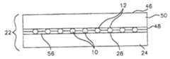
- FIG. 4is a schematic side elevation view of an electronic assembly assembled using a component constructed in accordance with the invention.
- FIG. 5Ais an enlarged cross sectional view equivalent to FIG. 3A of an alternate embodiment polymer support ring reinforcing a contact ball on a semiconductor component;
- FIG. 5Bis a cross sectional view of the polymer support ring taken along section line 5 B— 5 B of FIG. 5 A:
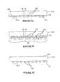
- FIGS. 6A-6Bare schematic cross sectional views illustrating steps in a method for fabricating the semiconductor component with a polymer layer as in FIG. 2A ;
- FIGS. 7A-7Care schematic cross sectional views illustrating steps in a method for fabricating the semiconductor component with polymer rings as in FIG. 5 A.
- semiconductor component 46constructed in accordance with the invention is illustrated.
- semiconductor componentrefers to an element, or an assembly, that includes a semiconductor die.
- the semiconductor component 46can comprise a chip scale package, a BGA device, a bare semiconductor die, a semiconductor wafer containing semiconductor dice, or a panel or wafer containing semiconductor packages.
- the component 46includes a substrate 50 , and a plurality of bonding pads 12 and external contacts 10 formed on a surface 52 of the substrate 50 .
- Representative materials for the component substrate 50include ceramic, silicon, and glass filled plastics such as FR-4.
- Representative materials for the bonding pads 12include molybdenum, copper and nickel.
- the external contacts 10can comprise any of the embodiments shown in FIGS. 1A-1F .
- the external contacts 10are in electrical communication with integrated circuits, and other electrical elements, contained on the component 46 .
- the external contacts 10can be arranged in a dense grid array, such as a ball grid array (BGA), or a fine ball grid array (FBGA).
- BGAball grid array
- FBGAfine ball grid array
- the external contactsare shown in array of four rows and nine columns.
- the arraycan include as many, or as few, rows and columns of external contacts 10 as required, and can include from several to hundreds, or more, external contacts 10 .
- a pitch of the external contacts 10can be selected as required.
- the external contacts 10can have a center to center pitch as small as about 0.004-in (0.100 mm) or smaller.
- the component 46also includes a polymer support member in the form of a polymer layer 48 formed on the surface 52 of the substrate 50 .
- the polymer layer 48is configured to support the external contacts 10 , and to rigidify and strengthen the bonding of the external contacts 10 to the bonding pads 12 on the component 46 .
- the polymer layer 48absorbs forces acting on the external contacts 10 .
- the polymer layer 48transfers forces occurring at the interfaces of the external contacts 10 with the bonding pads 12 and redistributes the forces into the center, or full volume, of the external contacts 10 .
- a component 46 Aincludes a substrate 50 A, bonding pads 12 A on the substrate 50 A, and contact balls 10 A bonded to the bonding pads 12 A using eutectic solder fillets 16 A.
- the contact balls 10 Acan comprise solder balls constructed and bonded to the bonding pads 12 A on the substrate 50 A, substantially as previously described and shown in FIG. 1 A.
- the component 46 Aincludes a polymer layer 48 A configured to strengthen and rigidify the contact balls 46 A.
- the polymer layer 48 Ahas a thickness T that is less than a height H of the contact balls 10 A. This permits tip portions 64 A of the contact balls 10 A to be bonded to mating contact pads 28 ( FIG. 4 ) on a supporting substrate 24 (FIG. 4 ).
- an underfill layer 56FIG. 4 can be placed between the component 46 A and the supporting substrate 24 (FIG. 4 ), if desired.
- a representative range for the height “H” of the contact balls 10 Acan be from about 0.004-in (0.100 mm) to 0.030-in (0.762 mm).
- a representative range for the thickness T of the polymer layer 48 Acan be from about 0.002-in (0.050 mm) to 0.025-in (0.635 mm).
- the polymer layer 48 Acomprises a resilient material that adheres to, and encompasses base portions 66 A of the contact balls 10 A, such that forces can be efficiently absorbed by the polymer layer 48 A, and transmitted away from the interface of the contact balls 10 A with the bonding pads 12 A.
- base portionsrefers to portions of the contact balls 10 A configured for bonding to the bonding pads 12 A.
- tip portionsrefers to exposed portions of the contact balls 10 A configured for bonding to contact pads 28 ( FIG. 4 ) on a supporting substrate 24 (FIG. 4 ).
- the polymer layer 48 Acomprises a curable material, such as polyimide, that can be deposited in viscous form, and then cured to harden.
- the polymer layer 48 Acan also comprise a photoimageable material, such as a thick film resist, to permit blanket deposition, and then removal from selected portions of the surface 52 A of the component substrate 50 A by development of the material.
- an alternate embodiment component 46 Bincludes contact bumps 10 B formed on bonding pads 12 B on a component substrate 50 B, substantially as previously described, and shown in FIG. 1 B.
- the component 46 Bincludes a polymer layer 48 B that adheres to and encompasses base portions 66 B of the contact bumps 10 B.
- the polymer layer 48 Bhas a thickness T 1 that is less than a height H 1 of the contact bumps 10 B such that tip portions of the contact bumps 10 B are left exposed for bonding.
- the thickness T 1is about one half the height H 1 such that a surface of the polymer layer 48 B is coincident to a plane through the centers of the contact bumps 10 B.
- the thickness T 1can be less than one half the height with from one fourth to one half being preferred.
- an alternate embodiment component 46 Cincludes contact columns 10 C formed on bonding pads 12 C on a component substrate 50 C, substantially as previously described, and shown in FIG. 1 C.
- the component 46 Cincludes a polymer layer 48 C that adheres to and encompasses base portions 66 C of the contact columns 10 C.
- the polymer layer 48 Chas a thickness T 2 that is less that a height H 2 of the contact columns 10 C such that tip portions 64 C of the contact columns 10 C are exposed for bonding. In FIG. 3C , the thickness T 2 is about one half the height H 2 .
- the thickness T 2can be substantially less than one half the height H 2 (e.g., one fourth the height H 2 or less) and still perform adequately.
- an alternate embodiment component 46 Dincludes TAB contact bumps 10 D formed on multi layered TAB tape 38 , substantially as previously described and shown in FIG. 1 D.
- the component 46 Dincludes a polymer layer 48 D that adheres to the TAB tape 38 and encompasses base portions 66 D of the contact bumps 10 D on the polymer tape 38 .
- the polymer layer 48 Dhas a thickness T 3 that is less than a height H 3 of the contact bumps 10 D such that tip portions 64 D of the contact bumps 10 D are exposed for bonding.
- the thickness T 3is about one fourth to one half the height H 3 or less.
- an alternate embodiment component 46 Eincludes contact balls 10 E formed on bonding pads 12 E in openings in a solder mask 40 on a component substrate 50 E, substantially as previously described, and shown in FIG. 1 E.
- the component 46 Eincludes a polymer layer 48 E bonded to the solder mask 40 and encompassing base portions 66 E of the contact balls 10 E.
- the polymer layer 48 Ehas a thickness T 4 that is less than a height H 4 of the contact balls 10 E such that tip portions 64 E of the contact balls 10 E are exposed for bonding.
- the thickness T 4is about one fourth to one half the height H 4 .
- an alternate embodiment component 46 Fincludes stud contact bumps 10 F formed on polymer film 44 on a component substrate 50 F, substantially as previously described, and shown in FIG. 1 F.
- the component 46 Fincludes a polymer layer 48 F that adheres to the component substrate 50 F and encompasses base portions 66 F of the stud contact bumps 10 F.
- the polymer layer 48 Fhas a thickness T 5 that is less than a height H 5 of the stud contact bumps 10 F such that tip portions 64 F of the stud contact bumps 10 F are exposed for bonding.
- the thickness T 5is about one fourth to one half the height H 5 .
- the component 46is shown surface mounted to a supporting substrate 24 to form an electronic assembly 22 .
- the external contacts 10 on the component 46are bonded to contact pads 28 on the supporting substrate 24 substantially as previously described.
- an underfill layer 56optionally fills the gap between the component 46 and the supporting substrate 24 .
- the polymer layer 48strengthens and rigidifies the bonding of the external contacts 10 , to the bonding pads 16 on the component substrate 50 . Further, the polymer layer 48 absorbs and resists forces acting on the external contacts 10 , such that separation from the bonding pads 16 is less likely to occur.
- an alternate embodiment semiconductor component 46 Gincludes a substrate 50 G, and a plurality of bonding pads 12 G on the substrate 50 G.
- the component 46 Fincludes a plurality of contact balls 10 G bonded to the bonding pads 12 G.
- the component 46 Galso includes a polymer support member in the form of a plurality of polymer rings 54 configured to support and rigidify the contact balls 10 G.
- the contact balls 10 Gare initially attached to the bonding pads 12 G such that spaces 62 are present between base portions 66 G of the contact balls 10 G and the bonding pads 12 G.
- This configurationcan be achieved by bonding the contact balls 10 G to the bonding pads 12 G using a eutectic solder fillet 16 G.
- This configurationcan also be achieved by forming the contact balls 10 G directly on the bonding pads 12 G using a deposition process such as electroless or electrodeposition, or by using pre-formed eutectic balls substantially as previously described.
- the polymer rings 54substantially fill the spaces 62 between the contact balls 10 G and bonding pads 12 G.
- the polymer ringsfunction substantially as previously described for polymer layer 48 to strengthen and rigidify the bonds to the contact balls 10 G.
- a thickness T 6 of the polymer rings 54is approximately equal to one half a height H 6 of the contact balls 10 G such that tip portions 64 G of the contact balls 10 G remain exposed for bonding.
- the thickness T 6 of the polymer rings 54is from one fourth to one half the height H 6 of the contact balls 10 G.
- the polymer rings 54can be formed with this thickness using a photoimageable polymer, and a developing process to be hereinafter described.
- the component substrate 50can be provided with the external contacts 10 bonded to the bonding pads 16 .
- the external contacts 10 on the component substrate 50can be in one of the configurations shown in FIGS. 3A-3F , or any other conventional configuration.
- any conventional bonding processsuch as solder reflow, laser reflow, welding, brazing, or conductive adhesive bonding, can be used to bond the external contacts 10 to the bonding pads 16 .
- the component substrate 50is provided as a wafer, a panel, a strip, or a leadframe, containing multiple substrates 50 .
- the component 46can be singulated using a suitable process such as cutting, shearing or etching.
- the polymer layer 48can be blanket deposited on the component substrate 50 in a viscous state.
- Suitable materials for the polymer layer 48include curable polymers such as polyimide, silicone, epoxy, and thick film resists.
- a thickness of the polymer layer 48can be selected substantially as previously described. This thickness can be controlled by dispensing a required volume of material onto the substrate 50 , and then spinning if required, using a suitable apparatus, such as a spin coater or meniscus coater.
- the deposition processcan be controlled such that the polymer layer 48 adheres to the base portions 66 of the external contacts 10 , but does not completely cover the tip portions 64 , substantially as previously described.
- a curing stepcan be performed to cure the polymer layer 48 .
- the curing stepcan be performed by heating the polymer layer 48 to a required temperature for a required time period.
- the curing processcan be performed by outgassing of a solvent.
- the polymer layer 48can cure with a curved, or meniscus shape, during adherence to the base portions 66 of the external contacts 10 .
- the component substrate 50 Gcan be provided.
- this fabrication processis preferably performed on multiple substrates 50 G contained on a wafer, a panel, a strip or a leadframe.
- the external contactscomprise contact balls 10 G that are bonded to the bonding pads 12 G, such that spaces 62 are present between the curved base portions 66 G of the contact balls 10 G, and the bonding pads 12 G.
- Such a configurationcan be achieved by bonding the contact balls 10 G using eutectic solder fillets 16 G (FIG. 5 A).
- Such a configurationcan also be achieved by forming the contact balls 10 G directly on the bonding pads 12 G using a deposition process such as electroless or electrodeposition through openings in a mask, or by using eutectic solder balls substantially as previously described.
- a thick film resist 58can be blanket deposited on the component substrate 50 G, on the contact balls 10 G and in the spaces between the contact balls 10 G.
- One suitable thick film resistis a negative tone resist sold by Shell Chemical under the trademark “EPON RESIN SU-8”.
- the resistcan be deposited in layers to a thickness of from about 3-50 mils.
- the resistalso includes an organic solvent (e.g., gamma-butyloracton), and a photoinitiator.
- a conventional resist coating apparatussuch as a spin coater, or a meniscus coater, can be used to deposit the resist in viscous form onto the substrate 50 G.
- the deposited resistcan then be partially hardened by heating to about 95° C. for about 15 minutes or longer.
- the resist 58can be exposed using an exposure energy 60 .
- Exposure of the resist 58can be performed with a conventional UV mask writer using a suitable UV dose.
- a representative UV dose for the previously described resist formulationis about 165 mJ/cm 2 .
- the resist present in the spaces 62is “shadowed” or “protected” by the contact balls 10 G such that this material remains unexposed.
- the resist 58can be developed using a suitable developer.
- a suitable developer for developing the previously described resist formulationis a solution of PGMEA (propyleneglycol-monomethylether-acetate).
- PGMEApropyleneglycol-monomethylether-acetate.
- Developing of the resist 58forms the support rings 54 leaving the tip portions 64 G exposed for bonding.
- the support rings 54can be fully hardened.
- a “full cure”can be performed with a hard bake at about 200° C. for about 30 minutes.
- the inventionprovides an improved semiconductor component and method of fabrication.
- the componentincludes external contacts and a polymer support member designed to strengthen and rigidify the external contacts.
Landscapes
- Engineering & Computer Science (AREA)
- Microelectronics & Electronic Packaging (AREA)
- Computer Hardware Design (AREA)
- Power Engineering (AREA)
- Manufacturing & Machinery (AREA)
- Physics & Mathematics (AREA)
- Condensed Matter Physics & Semiconductors (AREA)
- General Physics & Mathematics (AREA)
- Electric Connection Of Electric Components To Printed Circuits (AREA)
- Wire Bonding (AREA)
Abstract
Description
Claims (18)
Priority Applications (1)
| Application Number | Priority Date | Filing Date | Title |
|---|---|---|---|
| US10/693,380US6909194B2 (en) | 1999-08-27 | 2003-10-24 | Electronic assembly having semiconductor component with polymer support member and method of fabrication |
Applications Claiming Priority (4)
| Application Number | Priority Date | Filing Date | Title |
|---|---|---|---|
| US09/384,783US6118179A (en) | 1999-08-27 | 1999-08-27 | Semiconductor component with external contact polymer support member and method of fabrication |
| US09/440,380US6180504B1 (en) | 1999-08-27 | 1999-11-15 | Method for fabricating a semiconductor component with external polymer support layer |
| US09/653,366US6756253B1 (en) | 1999-08-27 | 2000-09-01 | Method for fabricating a semiconductor component with external contact polymer support layer |
| US10/693,380US6909194B2 (en) | 1999-08-27 | 2003-10-24 | Electronic assembly having semiconductor component with polymer support member and method of fabrication |
Related Parent Applications (1)
| Application Number | Title | Priority Date | Filing Date |
|---|---|---|---|
| US09/653,366ContinuationUS6756253B1 (en) | 1999-08-27 | 2000-09-01 | Method for fabricating a semiconductor component with external contact polymer support layer |
Publications (2)
| Publication Number | Publication Date |
|---|---|
| US20040087077A1 US20040087077A1 (en) | 2004-05-06 |
| US6909194B2true US6909194B2 (en) | 2005-06-21 |
Family
ID=32511128
Family Applications (2)
| Application Number | Title | Priority Date | Filing Date |
|---|---|---|---|
| US09/653,366Expired - LifetimeUS6756253B1 (en) | 1999-08-27 | 2000-09-01 | Method for fabricating a semiconductor component with external contact polymer support layer |
| US10/693,380Expired - LifetimeUS6909194B2 (en) | 1999-08-27 | 2003-10-24 | Electronic assembly having semiconductor component with polymer support member and method of fabrication |
Family Applications Before (1)
| Application Number | Title | Priority Date | Filing Date |
|---|---|---|---|
| US09/653,366Expired - LifetimeUS6756253B1 (en) | 1999-08-27 | 2000-09-01 | Method for fabricating a semiconductor component with external contact polymer support layer |
Country Status (1)
| Country | Link |
|---|---|
| US (2) | US6756253B1 (en) |
Cited By (40)
| Publication number | Priority date | Publication date | Assignee | Title |
|---|---|---|---|---|
| US20050161795A1 (en)* | 2003-02-07 | 2005-07-28 | Ziptronix | Room temperature metal direct bonding |
| US20050236704A1 (en)* | 2004-04-27 | 2005-10-27 | Jeng-Da Wu | Chip package structure and process for fabricating the same |
| US20080081397A1 (en)* | 2006-09-28 | 2008-04-03 | Philips Lumileds Lighting Company, Llc | Process for Preparing a Semiconductor Structure for Mounting |
| US20090230553A1 (en)* | 2008-03-14 | 2009-09-17 | Infineon Technologies Ag | Semiconductor device including adhesive covered element |
| US20130207240A1 (en)* | 2011-06-09 | 2013-08-15 | Xintec Inc. | Chip package structure and manufacturing method thereof |
| US8791556B2 (en) | 2012-03-29 | 2014-07-29 | Stats Chippac Ltd. | Integrated circuit packaging system with routable circuitry and method of manufacture thereof |
| US9716033B2 (en) | 2005-08-11 | 2017-07-25 | Ziptronix, Inc. | 3D IC method and device |
| US9953941B2 (en) | 2015-08-25 | 2018-04-24 | Invensas Bonding Technologies, Inc. | Conductive barrier direct hybrid bonding |
| US10580735B2 (en) | 2016-10-07 | 2020-03-03 | Xcelsis Corporation | Stacked IC structure with system level wiring on multiple sides of the IC die |
| US10580757B2 (en) | 2016-10-07 | 2020-03-03 | Xcelsis Corporation | Face-to-face mounted IC dies with orthogonal top interconnect layers |
| US10586786B2 (en) | 2016-10-07 | 2020-03-10 | Xcelsis Corporation | 3D chip sharing clock interconnect layer |
| US10593667B2 (en) | 2016-10-07 | 2020-03-17 | Xcelsis Corporation | 3D chip with shielded clock lines |
| US10600691B2 (en) | 2016-10-07 | 2020-03-24 | Xcelsis Corporation | 3D chip sharing power interconnect layer |
| US10600735B2 (en) | 2016-10-07 | 2020-03-24 | Xcelsis Corporation | 3D chip sharing data bus |
| US10600780B2 (en) | 2016-10-07 | 2020-03-24 | Xcelsis Corporation | 3D chip sharing data bus circuit |
| US10607136B2 (en) | 2017-08-03 | 2020-03-31 | Xcelsis Corporation | Time borrowing between layers of a three dimensional chip stack |
| US10672744B2 (en) | 2016-10-07 | 2020-06-02 | Xcelsis Corporation | 3D compute circuit with high density Z-axis interconnects |
| US10672663B2 (en) | 2016-10-07 | 2020-06-02 | Xcelsis Corporation | 3D chip sharing power circuit |
| US10672743B2 (en)* | 2016-10-07 | 2020-06-02 | Xcelsis Corporation | 3D Compute circuit with high density z-axis interconnects |
| US10672745B2 (en)* | 2016-10-07 | 2020-06-02 | Xcelsis Corporation | 3D processor |
| US20200294962A1 (en)* | 2018-02-15 | 2020-09-17 | Osram Oled Gmbh | Method for Producing a Connection Between Component Parts, and Component Made of Component Parts |
| US10840205B2 (en) | 2017-09-24 | 2020-11-17 | Invensas Bonding Technologies, Inc. | Chemical mechanical polishing for hybrid bonding |
| US11011494B2 (en) | 2018-08-31 | 2021-05-18 | Invensas Bonding Technologies, Inc. | Layer structures for making direct metal-to-metal bonds at low temperatures in microelectronics |
| US11158573B2 (en) | 2018-10-22 | 2021-10-26 | Invensas Bonding Technologies, Inc. | Interconnect structures |
| US11244920B2 (en) | 2018-12-18 | 2022-02-08 | Invensas Bonding Technologies, Inc. | Method and structures for low temperature device bonding |
| US11289333B2 (en) | 2016-10-07 | 2022-03-29 | Xcelsis Corporation | Direct-bonded native interconnects and active base die |
| US11393779B2 (en) | 2018-06-13 | 2022-07-19 | Invensas Bonding Technologies, Inc. | Large metal pads over TSV |
| US11515279B2 (en) | 2018-04-11 | 2022-11-29 | Adeia Semiconductor Bonding Technologies Inc. | Low temperature bonded structures |
| US11599299B2 (en) | 2019-11-19 | 2023-03-07 | Invensas Llc | 3D memory circuit |
| US11710718B2 (en) | 2015-07-10 | 2023-07-25 | Adeia Semiconductor Technologies Llc | Structures and methods for low temperature bonding using nanoparticles |
| US11728313B2 (en) | 2018-06-13 | 2023-08-15 | Adeia Semiconductor Bonding Technologies Inc. | Offset pads over TSV |
| US11735523B2 (en) | 2020-05-19 | 2023-08-22 | Adeia Semiconductor Bonding Technologies Inc. | Laterally unconfined structure |
| US11804377B2 (en) | 2018-04-05 | 2023-10-31 | Adeia Semiconductor Bonding Technologies, Inc. | Method for preparing a surface for direct-bonding |
| US11894326B2 (en) | 2017-03-17 | 2024-02-06 | Adeia Semiconductor Bonding Technologies Inc. | Multi-metal contact structure |
| US11908739B2 (en) | 2017-06-05 | 2024-02-20 | Adeia Semiconductor Technologies Llc | Flat metal features for microelectronics applications |
| US11929347B2 (en) | 2020-10-20 | 2024-03-12 | Adeia Semiconductor Technologies Llc | Mixed exposure for large die |
| US11973056B2 (en) | 2016-10-27 | 2024-04-30 | Adeia Semiconductor Technologies Llc | Methods for low temperature bonding using nanoparticles |
| US12100676B2 (en) | 2018-04-11 | 2024-09-24 | Adeia Semiconductor Bonding Technologies Inc. | Low temperature bonded structures |
| US12211809B2 (en) | 2020-12-30 | 2025-01-28 | Adeia Semiconductor Bonding Technologies Inc. | Structure with conductive feature and method of forming same |
| US12381128B2 (en) | 2020-12-28 | 2025-08-05 | Adeia Semiconductor Bonding Technologies Inc. | Structures with through-substrate vias and methods for forming the same |
Families Citing this family (11)
| Publication number | Priority date | Publication date | Assignee | Title |
|---|---|---|---|---|
| US7449307B2 (en)* | 2002-10-28 | 2008-11-11 | Transform Pharmaceuticals, Inc. | Raised surface assay plate |
| US7202541B2 (en)* | 2004-04-29 | 2007-04-10 | Hewlett-Packard Development Company, L.P. | Apparatus and method for transverse characterization of materials |
| WO2006063219A2 (en)* | 2004-12-09 | 2006-06-15 | Pro-Health, Inc. | Product and method for oral administration of nutraceuticals |
| US7160798B2 (en)* | 2005-02-24 | 2007-01-09 | Freescale Semiconductor, Inc. | Method of making reinforced semiconductor package |
| US20080308932A1 (en)* | 2007-06-12 | 2008-12-18 | Taiwan Semiconductor Manufacturing Co., Ltd. | Semiconductor package structures |
| KR101680082B1 (en) | 2010-05-07 | 2016-11-29 | 삼성전자 주식회사 | Wafer level package and methods for fabricating the same |
| US8432034B2 (en) | 2011-05-25 | 2013-04-30 | International Business Machines Corporation | Use of a local constraint to enhance attachment of an IC device to a mounting platform |
| US8867223B2 (en) | 2011-08-26 | 2014-10-21 | Dell Products, Lp | System and method for a high retention module interface |
| US8749043B2 (en)* | 2012-03-01 | 2014-06-10 | Taiwan Semiconductor Manufacturing Company, Ltd. | Package on package structure |
| KR102458034B1 (en) | 2015-10-16 | 2022-10-25 | 삼성전자주식회사 | Semiconductor package, Method of fabricating the Semiconductor package, And Semiconductor module |
| CN114515903A (en)* | 2022-03-04 | 2022-05-20 | 中国电子科技集团公司第三十八研究所 | Laser column planting method for CCGA high-lead welded column |
Citations (26)
| Publication number | Priority date | Publication date | Assignee | Title |
|---|---|---|---|---|
| US5385636A (en) | 1993-03-05 | 1995-01-31 | Alcatel N.V. | Method of forming a metal contact on a projection on a semiconductor substrate |
| US5674785A (en) | 1995-11-27 | 1997-10-07 | Micron Technology, Inc. | Method of producing a single piece package for semiconductor die |
| US5677566A (en) | 1995-05-08 | 1997-10-14 | Micron Technology, Inc. | Semiconductor chip package |
| US5763939A (en) | 1994-09-30 | 1998-06-09 | Nec Corporation | Semiconductor device having a perforated base film sheet |
| US5783461A (en) | 1996-10-03 | 1998-07-21 | Micron Technology, Inc. | Temporary semiconductor package having hard-metal, dense-array ball contacts and method of fabrication |
| US5811879A (en) | 1996-06-26 | 1998-09-22 | Micron Technology, Inc. | Stacked leads-over-chip multi-chip module |
| US5817530A (en)* | 1996-05-20 | 1998-10-06 | Micron Technology, Inc. | Use of conductive lines on the back side of wafers and dice for semiconductor interconnects |
| US5834945A (en) | 1996-12-31 | 1998-11-10 | Micron Technology, Inc. | High speed temporary package and interconnect for testing semiconductor dice and method of fabrication |
| US5885849A (en) | 1995-03-28 | 1999-03-23 | Tessera, Inc. | Methods of making microelectronic assemblies |
| WO1999021226A1 (en) | 1997-10-20 | 1999-04-29 | Flip Chip Technologies, L.L.C. | Chip scale package using large ductile solder balls |
| US5925930A (en) | 1996-05-21 | 1999-07-20 | Micron Technology, Inc. | IC contacts with palladium layer and flexible conductive epoxy bumps |
| US5956605A (en) | 1996-09-20 | 1999-09-21 | Micron Technology, Inc. | Use of nitrides for flip-chip encapsulation |
| US6059173A (en) | 1998-03-05 | 2000-05-09 | International Business Machines Corporation | Micro grid array solder interconnection structure for second level packaging joining a module and printed circuit board |
| US6063647A (en) | 1997-12-08 | 2000-05-16 | 3M Innovative Properties Company | Method for making circuit elements for a z-axis interconnect |
| US6118179A (en) | 1999-08-27 | 2000-09-12 | Micron Technology, Inc. | Semiconductor component with external contact polymer support member and method of fabrication |
| US6137164A (en)* | 1998-03-16 | 2000-10-24 | Texas Instruments Incorporated | Thin stacked integrated circuit device |
| US6204080B1 (en) | 1997-10-31 | 2001-03-20 | Daewoo Electronics Co., Ltd. | Method for manufacturing thin film actuated mirror array in an optical projection system |
| US6294837B1 (en)* | 1997-12-18 | 2001-09-25 | Micron Technology, Inc. | Semiconductor interconnect having laser machined contacts |
| US6297560B1 (en) | 1996-10-31 | 2001-10-02 | Miguel Albert Capote | Semiconductor flip-chip assembly with pre-applied encapsulating layers |
| US6339254B1 (en)* | 1998-09-01 | 2002-01-15 | Texas Instruments Incorporated | Stacked flip-chip integrated circuit assemblage |
| US6353420B1 (en)* | 1999-04-28 | 2002-03-05 | Amerasia International Technology, Inc. | Wireless article including a plural-turn loop antenna |
| US6352881B1 (en) | 1999-07-22 | 2002-03-05 | National Semiconductor Corporation | Method and apparatus for forming an underfill adhesive layer |
| US6396136B2 (en)* | 1998-12-31 | 2002-05-28 | Texas Instruments Incorporated | Ball grid package with multiple power/ground planes |
| US6404643B1 (en)* | 1998-10-15 | 2002-06-11 | Amerasia International Technology, Inc. | Article having an embedded electronic device, and method of making same |
| US6524346B1 (en) | 1999-02-26 | 2003-02-25 | Micron Technology, Inc. | Stereolithographic method for applying materials to electronic component substrates and resulting structures |
| US6583354B2 (en) | 1999-04-27 | 2003-06-24 | International Business Machines Corporation | Method of reforming reformable members of an electronic package and the resultant electronic package |
Family Cites Families (1)
| Publication number | Priority date | Publication date | Assignee | Title |
|---|---|---|---|---|
| US6059170A (en)* | 1998-06-24 | 2000-05-09 | International Business Machines Corporation | Method and apparatus for insulating moisture sensitive PBGA's |
- 2000
- 2000-09-01USUS09/653,366patent/US6756253B1/ennot_activeExpired - Lifetime
- 2003
- 2003-10-24USUS10/693,380patent/US6909194B2/ennot_activeExpired - Lifetime
Patent Citations (29)
| Publication number | Priority date | Publication date | Assignee | Title |
|---|---|---|---|---|
| US5385636A (en) | 1993-03-05 | 1995-01-31 | Alcatel N.V. | Method of forming a metal contact on a projection on a semiconductor substrate |
| US5763939A (en) | 1994-09-30 | 1998-06-09 | Nec Corporation | Semiconductor device having a perforated base film sheet |
| US5885849A (en) | 1995-03-28 | 1999-03-23 | Tessera, Inc. | Methods of making microelectronic assemblies |
| US5677566A (en) | 1995-05-08 | 1997-10-14 | Micron Technology, Inc. | Semiconductor chip package |
| US5739585A (en) | 1995-11-27 | 1998-04-14 | Micron Technology, Inc. | Single piece package for semiconductor die |
| US5674785A (en) | 1995-11-27 | 1997-10-07 | Micron Technology, Inc. | Method of producing a single piece package for semiconductor die |
| US5817530A (en)* | 1996-05-20 | 1998-10-06 | Micron Technology, Inc. | Use of conductive lines on the back side of wafers and dice for semiconductor interconnects |
| US5925930A (en) | 1996-05-21 | 1999-07-20 | Micron Technology, Inc. | IC contacts with palladium layer and flexible conductive epoxy bumps |
| US5811879A (en) | 1996-06-26 | 1998-09-22 | Micron Technology, Inc. | Stacked leads-over-chip multi-chip module |
| US5956605A (en) | 1996-09-20 | 1999-09-21 | Micron Technology, Inc. | Use of nitrides for flip-chip encapsulation |
| US5783461A (en) | 1996-10-03 | 1998-07-21 | Micron Technology, Inc. | Temporary semiconductor package having hard-metal, dense-array ball contacts and method of fabrication |
| US6297560B1 (en) | 1996-10-31 | 2001-10-02 | Miguel Albert Capote | Semiconductor flip-chip assembly with pre-applied encapsulating layers |
| US5834945A (en) | 1996-12-31 | 1998-11-10 | Micron Technology, Inc. | High speed temporary package and interconnect for testing semiconductor dice and method of fabrication |
| WO1999021226A1 (en) | 1997-10-20 | 1999-04-29 | Flip Chip Technologies, L.L.C. | Chip scale package using large ductile solder balls |
| US6204080B1 (en) | 1997-10-31 | 2001-03-20 | Daewoo Electronics Co., Ltd. | Method for manufacturing thin film actuated mirror array in an optical projection system |
| US6063647A (en) | 1997-12-08 | 2000-05-16 | 3M Innovative Properties Company | Method for making circuit elements for a z-axis interconnect |
| US6294837B1 (en)* | 1997-12-18 | 2001-09-25 | Micron Technology, Inc. | Semiconductor interconnect having laser machined contacts |
| US6059173A (en) | 1998-03-05 | 2000-05-09 | International Business Machines Corporation | Micro grid array solder interconnection structure for second level packaging joining a module and printed circuit board |
| US6137164A (en)* | 1998-03-16 | 2000-10-24 | Texas Instruments Incorporated | Thin stacked integrated circuit device |
| US6339254B1 (en)* | 1998-09-01 | 2002-01-15 | Texas Instruments Incorporated | Stacked flip-chip integrated circuit assemblage |
| US6404643B1 (en)* | 1998-10-15 | 2002-06-11 | Amerasia International Technology, Inc. | Article having an embedded electronic device, and method of making same |
| US6396136B2 (en)* | 1998-12-31 | 2002-05-28 | Texas Instruments Incorporated | Ball grid package with multiple power/ground planes |
| US6524346B1 (en) | 1999-02-26 | 2003-02-25 | Micron Technology, Inc. | Stereolithographic method for applying materials to electronic component substrates and resulting structures |
| US20030102566A1 (en) | 1999-02-26 | 2003-06-05 | Farnworth Warren M. | Stereolithographic method for applying materials to electronic component substrates and resulting structures |
| US6583354B2 (en) | 1999-04-27 | 2003-06-24 | International Business Machines Corporation | Method of reforming reformable members of an electronic package and the resultant electronic package |
| US6353420B1 (en)* | 1999-04-28 | 2002-03-05 | Amerasia International Technology, Inc. | Wireless article including a plural-turn loop antenna |
| US6352881B1 (en) | 1999-07-22 | 2002-03-05 | National Semiconductor Corporation | Method and apparatus for forming an underfill adhesive layer |
| US6118179A (en) | 1999-08-27 | 2000-09-12 | Micron Technology, Inc. | Semiconductor component with external contact polymer support member and method of fabrication |
| US6180504B1 (en) | 1999-08-27 | 2001-01-30 | Micron Technology, Inc. | Method for fabricating a semiconductor component with external polymer support layer |
Non-Patent Citations (3)
| Title |
|---|
| John Baliga, "Assembly & Packaging Wafer-Level Packages to Include Solder Ball Support", Nov. 27, 2000, pp. 1-2, Technology News. |
| Lau, John H., Ball Grid Array Technology, 1995, pp. 33, 47, 56, 133, 180, 247, 279, 475, 476-480, McGraw-Hill, Inc., United States. |
| Tummala, Rao R., "Chip-to-Package Interconnections", Microelectronics Packaging Handbook, 1989, pp. 366-368, VanNostrand Reinhold (publisher), New York, NY. |
Cited By (97)
| Publication number | Priority date | Publication date | Assignee | Title |
|---|---|---|---|---|
| US7602070B2 (en)* | 2003-02-07 | 2009-10-13 | Ziptronix, Inc. | Room temperature metal direct bonding |
| US20070232023A1 (en)* | 2003-02-07 | 2007-10-04 | Ziptronix, Inc. | Room temperature metal direct bonding |
| US10141218B2 (en) | 2003-02-07 | 2018-11-27 | Invensas Bonding Technologies, Inc. | Room temperature metal direct bonding |
| US8846450B2 (en) | 2003-02-07 | 2014-09-30 | Ziptronix, Inc. | Room temperature metal direct bonding |
| US8524533B2 (en) | 2003-02-07 | 2013-09-03 | Ziptronix, Inc. | Room temperature metal direct bonding |
| US7842540B2 (en) | 2003-02-07 | 2010-11-30 | Ziptronix, Inc. | Room temperature metal direct bonding |
| US20110041329A1 (en)* | 2003-02-07 | 2011-02-24 | Ziptronix, Inc. | Room temperature metal direct bonding |
| US20050161795A1 (en)* | 2003-02-07 | 2005-07-28 | Ziptronix | Room temperature metal direct bonding |
| US9385024B2 (en) | 2003-02-07 | 2016-07-05 | Ziptronix, Inc. | Room temperature metal direct bonding |
| US20050236704A1 (en)* | 2004-04-27 | 2005-10-27 | Jeng-Da Wu | Chip package structure and process for fabricating the same |
| US10147641B2 (en) | 2005-08-11 | 2018-12-04 | Invensas Bonding Technologies, Inc. | 3D IC method and device |
| US11289372B2 (en) | 2005-08-11 | 2022-03-29 | Invensas Bonding Technologies, Inc. | 3D IC method and device |
| US11011418B2 (en) | 2005-08-11 | 2021-05-18 | Invensas Bonding Technologies, Inc. | 3D IC method and device |
| US11515202B2 (en) | 2005-08-11 | 2022-11-29 | Adeia Semiconductor Bonding Technologies Inc. | 3D IC method and device |
| US9716033B2 (en) | 2005-08-11 | 2017-07-25 | Ziptronix, Inc. | 3D IC method and device |
| US9111950B2 (en)* | 2006-09-28 | 2015-08-18 | Philips Lumileds Lighting Company, Llc | Process for preparing a semiconductor structure for mounting |
| US20080081397A1 (en)* | 2006-09-28 | 2008-04-03 | Philips Lumileds Lighting Company, Llc | Process for Preparing a Semiconductor Structure for Mounting |
| US9899578B2 (en) | 2006-09-28 | 2018-02-20 | Lumileds Llc | Process for preparing a semiconductor structure for mounting |
| US8659154B2 (en) | 2008-03-14 | 2014-02-25 | Infineon Technologies Ag | Semiconductor device including adhesive covered element |
| US9984900B2 (en) | 2008-03-14 | 2018-05-29 | Infineon Technologies Ag | Semiconductor device including at least one element |
| US20090230553A1 (en)* | 2008-03-14 | 2009-09-17 | Infineon Technologies Ag | Semiconductor device including adhesive covered element |
| US8779558B2 (en)* | 2011-06-09 | 2014-07-15 | Xintec Inc. | Chip package structure and manufacturing method thereof |
| US20130207240A1 (en)* | 2011-06-09 | 2013-08-15 | Xintec Inc. | Chip package structure and manufacturing method thereof |
| US8791556B2 (en) | 2012-03-29 | 2014-07-29 | Stats Chippac Ltd. | Integrated circuit packaging system with routable circuitry and method of manufacture thereof |
| US11710718B2 (en) | 2015-07-10 | 2023-07-25 | Adeia Semiconductor Technologies Llc | Structures and methods for low temperature bonding using nanoparticles |
| US12381168B2 (en) | 2015-08-25 | 2025-08-05 | Adeia Semiconductor Bonding Technologies Inc. | Conductive barrier direct hybrid bonding |
| US11830838B2 (en) | 2015-08-25 | 2023-11-28 | Adeia Semiconductor Bonding Technologies Inc. | Conductive barrier direct hybrid bonding |
| US10262963B2 (en) | 2015-08-25 | 2019-04-16 | Invensas Bonding Technologies, Inc. | Conductive barrier direct hybrid bonding |
| US11264345B2 (en) | 2015-08-25 | 2022-03-01 | Invensas Bonding Technologies, Inc. | Conductive barrier direct hybrid bonding |
| US9953941B2 (en) | 2015-08-25 | 2018-04-24 | Invensas Bonding Technologies, Inc. | Conductive barrier direct hybrid bonding |
| US10892252B2 (en) | 2016-10-07 | 2021-01-12 | Xcelsis Corporation | Face-to-face mounted IC dies with orthogonal top interconnect layers |
| US10580757B2 (en) | 2016-10-07 | 2020-03-03 | Xcelsis Corporation | Face-to-face mounted IC dies with orthogonal top interconnect layers |
| US10672663B2 (en) | 2016-10-07 | 2020-06-02 | Xcelsis Corporation | 3D chip sharing power circuit |
| US10672743B2 (en)* | 2016-10-07 | 2020-06-02 | Xcelsis Corporation | 3D Compute circuit with high density z-axis interconnects |
| US10672745B2 (en)* | 2016-10-07 | 2020-06-02 | Xcelsis Corporation | 3D processor |
| US11824042B2 (en) | 2016-10-07 | 2023-11-21 | Xcelsis Corporation | 3D chip sharing data bus |
| US12218059B2 (en) | 2016-10-07 | 2025-02-04 | Adeia Semiconductor Inc. | Stacked IC structure with orthogonal interconnect layers |
| US10593667B2 (en) | 2016-10-07 | 2020-03-17 | Xcelsis Corporation | 3D chip with shielded clock lines |
| US10600691B2 (en) | 2016-10-07 | 2020-03-24 | Xcelsis Corporation | 3D chip sharing power interconnect layer |
| US10886177B2 (en) | 2016-10-07 | 2021-01-05 | Xcelsis Corporation | 3D chip with shared clock distribution network |
| US11557516B2 (en) | 2016-10-07 | 2023-01-17 | Adeia Semiconductor Inc. | 3D chip with shared clock distribution network |
| US10950547B2 (en) | 2016-10-07 | 2021-03-16 | Xcelsis Corporation | Stacked IC structure with system level wiring on multiple sides of the IC die |
| US12293993B2 (en) | 2016-10-07 | 2025-05-06 | Adeia Semiconductor Inc. | 3D chip sharing data bus |
| US10978348B2 (en) | 2016-10-07 | 2021-04-13 | Xcelsis Corporation | 3D chip sharing power interconnect layer |
| US12401010B2 (en) | 2016-10-07 | 2025-08-26 | Adeia Semiconductor Inc. | 3D processor having stacked integrated circuit die |
| US10586786B2 (en) | 2016-10-07 | 2020-03-10 | Xcelsis Corporation | 3D chip sharing clock interconnect layer |
| US11152336B2 (en) | 2016-10-07 | 2021-10-19 | Xcelsis Corporation | 3D processor having stacked integrated circuit die |
| US11823906B2 (en) | 2016-10-07 | 2023-11-21 | Xcelsis Corporation | Direct-bonded native interconnects and active base die |
| US10600780B2 (en) | 2016-10-07 | 2020-03-24 | Xcelsis Corporation | 3D chip sharing data bus circuit |
| US10672744B2 (en) | 2016-10-07 | 2020-06-02 | Xcelsis Corporation | 3D compute circuit with high density Z-axis interconnects |
| US10600735B2 (en) | 2016-10-07 | 2020-03-24 | Xcelsis Corporation | 3D chip sharing data bus |
| US11289333B2 (en) | 2016-10-07 | 2022-03-29 | Xcelsis Corporation | Direct-bonded native interconnects and active base die |
| US10580735B2 (en) | 2016-10-07 | 2020-03-03 | Xcelsis Corporation | Stacked IC structure with system level wiring on multiple sides of the IC die |
| US12362182B2 (en) | 2016-10-07 | 2025-07-15 | Adeia Semiconductor Inc. | Direct-bonded native interconnects and active base die |
| US11881454B2 (en) | 2016-10-07 | 2024-01-23 | Adeia Semiconductor Inc. | Stacked IC structure with orthogonal interconnect layers |
| US11973056B2 (en) | 2016-10-27 | 2024-04-30 | Adeia Semiconductor Technologies Llc | Methods for low temperature bonding using nanoparticles |
| US12027487B2 (en) | 2016-10-27 | 2024-07-02 | Adeia Semiconductor Technologies Llc | Structures for low temperature bonding using nanoparticles |
| US11894326B2 (en) | 2017-03-17 | 2024-02-06 | Adeia Semiconductor Bonding Technologies Inc. | Multi-metal contact structure |
| US11908739B2 (en) | 2017-06-05 | 2024-02-20 | Adeia Semiconductor Technologies Llc | Flat metal features for microelectronics applications |
| US11176450B2 (en) | 2017-08-03 | 2021-11-16 | Xcelsis Corporation | Three dimensional circuit implementing machine trained network |
| US10970627B2 (en) | 2017-08-03 | 2021-04-06 | Xcelsis Corporation | Time borrowing between layers of a three dimensional chip stack |
| US12248869B2 (en) | 2017-08-03 | 2025-03-11 | Adeia Semiconductor Inc. | Three dimensional circuit implementing machine trained network |
| US10762420B2 (en) | 2017-08-03 | 2020-09-01 | Xcelsis Corporation | Self repairing neural network |
| US10719762B2 (en) | 2017-08-03 | 2020-07-21 | Xcelsis Corporation | Three dimensional chip structure implementing machine trained network |
| US11790219B2 (en) | 2017-08-03 | 2023-10-17 | Adeia Semiconductor Inc. | Three dimensional circuit implementing machine trained network |
| US10607136B2 (en) | 2017-08-03 | 2020-03-31 | Xcelsis Corporation | Time borrowing between layers of a three dimensional chip stack |
| US10840205B2 (en) | 2017-09-24 | 2020-11-17 | Invensas Bonding Technologies, Inc. | Chemical mechanical polishing for hybrid bonding |
| US11552041B2 (en) | 2017-09-24 | 2023-01-10 | Adeia Semiconductor Bonding Technologies Inc. | Chemical mechanical polishing for hybrid bonding |
| US12381173B2 (en) | 2017-09-24 | 2025-08-05 | Adeia Semiconductor Bonding Technologies Inc. | Direct hybrid bonding of substrates having microelectronic components with different profiles and/or pitches at the bonding interface |
| US11961820B2 (en)* | 2018-02-15 | 2024-04-16 | Osram Oled Gmbh | Method for producing a connection between component parts, and component made of component parts |
| US20200294962A1 (en)* | 2018-02-15 | 2020-09-17 | Osram Oled Gmbh | Method for Producing a Connection Between Component Parts, and Component Made of Component Parts |
| US11804377B2 (en) | 2018-04-05 | 2023-10-31 | Adeia Semiconductor Bonding Technologies, Inc. | Method for preparing a surface for direct-bonding |
| US12341018B2 (en) | 2018-04-05 | 2025-06-24 | Adeia Semiconductor Bonding Technologies Inc. | Method for preparing a surface for direct-bonding |
| US12132020B2 (en) | 2018-04-11 | 2024-10-29 | Adeia Semiconductor Bonding Technologies Inc. | Low temperature bonded structures |
| US11515279B2 (en) | 2018-04-11 | 2022-11-29 | Adeia Semiconductor Bonding Technologies Inc. | Low temperature bonded structures |
| US12100676B2 (en) | 2018-04-11 | 2024-09-24 | Adeia Semiconductor Bonding Technologies Inc. | Low temperature bonded structures |
| US12046571B2 (en) | 2018-04-11 | 2024-07-23 | Adeia Semiconductor Bonding Technologies Inc. | Low temperature bonded structures |
| US11955445B2 (en) | 2018-06-13 | 2024-04-09 | Adeia Semiconductor Bonding Technologies Inc. | Metal pads over TSV |
| US11728313B2 (en) | 2018-06-13 | 2023-08-15 | Adeia Semiconductor Bonding Technologies Inc. | Offset pads over TSV |
| US11393779B2 (en) | 2018-06-13 | 2022-07-19 | Invensas Bonding Technologies, Inc. | Large metal pads over TSV |
| US12243851B2 (en) | 2018-06-13 | 2025-03-04 | Adeia Semiconductor Bonding Technologies Inc. | Offset pads over TSV |
| US11749645B2 (en) | 2018-06-13 | 2023-09-05 | Adeia Semiconductor Bonding Technologies Inc. | TSV as pad |
| US12205926B2 (en) | 2018-06-13 | 2025-01-21 | Adeia Semiconductor Bonding Technologies Inc. | TSV as pad |
| US12136605B2 (en) | 2018-08-31 | 2024-11-05 | Adeia Semiconductor Bonding Technologies Inc. | Layer structures for making direct metal-to-metal bonds at low temperatures in microelectronics and method for forming the same |
| US11011494B2 (en) | 2018-08-31 | 2021-05-18 | Invensas Bonding Technologies, Inc. | Layer structures for making direct metal-to-metal bonds at low temperatures in microelectronics |
| US11756880B2 (en) | 2018-10-22 | 2023-09-12 | Adeia Semiconductor Bonding Technologies Inc. | Interconnect structures |
| US12125784B2 (en) | 2018-10-22 | 2024-10-22 | Adeia Semiconductor Bonding Technologies Inc. | Interconnect structures |
| US11158573B2 (en) | 2018-10-22 | 2021-10-26 | Invensas Bonding Technologies, Inc. | Interconnect structures |
| US11244920B2 (en) | 2018-12-18 | 2022-02-08 | Invensas Bonding Technologies, Inc. | Method and structures for low temperature device bonding |
| US12154880B2 (en) | 2018-12-18 | 2024-11-26 | Adeia Semiconductor Bonding Technologies Inc. | Method and structures for low temperature device bonding |
| US12293108B2 (en) | 2019-11-19 | 2025-05-06 | Adeia Semiconductor Technologies Llc | 3D memory circuit |
| US11599299B2 (en) | 2019-11-19 | 2023-03-07 | Invensas Llc | 3D memory circuit |
| US12033943B2 (en) | 2020-05-19 | 2024-07-09 | Adeia Semiconductor Bonding Technologies Inc. | Laterally unconfined structure |
| US11735523B2 (en) | 2020-05-19 | 2023-08-22 | Adeia Semiconductor Bonding Technologies Inc. | Laterally unconfined structure |
| US11929347B2 (en) | 2020-10-20 | 2024-03-12 | Adeia Semiconductor Technologies Llc | Mixed exposure for large die |
| US12381128B2 (en) | 2020-12-28 | 2025-08-05 | Adeia Semiconductor Bonding Technologies Inc. | Structures with through-substrate vias and methods for forming the same |
| US12211809B2 (en) | 2020-12-30 | 2025-01-28 | Adeia Semiconductor Bonding Technologies Inc. | Structure with conductive feature and method of forming same |
Also Published As
| Publication number | Publication date |
|---|---|
| US20040087077A1 (en) | 2004-05-06 |
| US6756253B1 (en) | 2004-06-29 |
Similar Documents
| Publication | Publication Date | Title |
|---|---|---|
| US6909194B2 (en) | Electronic assembly having semiconductor component with polymer support member and method of fabrication | |
| US6180504B1 (en) | Method for fabricating a semiconductor component with external polymer support layer | |
| JP4698125B2 (en) | Flip chip for substrate assembly without bumps and polymer layers | |
| US6190940B1 (en) | Flip chip assembly of semiconductor IC chips | |
| JP3320979B2 (en) | How to mount a device directly on a device carrier | |
| KR100545008B1 (en) | Semiconductor device, manufacturing method thereof and semiconductor device, manufacturing method thereof | |
| US5633535A (en) | Spacing control in electronic device assemblies | |
| JP3588027B2 (en) | Method of bonding IC chip to substrate | |
| US6008071A (en) | Method of forming solder bumps onto an integrated circuit device | |
| JP3262497B2 (en) | Chip mounted circuit card structure | |
| US6926191B2 (en) | Process for fabricating external contacts on semiconductor components | |
| US6441500B1 (en) | Semiconductor device having resin members provided separately corresponding to externally connecting electrodes | |
| US6319810B1 (en) | Method for forming solder bumps | |
| JP3450236B2 (en) | Semiconductor device and manufacturing method thereof | |
| JP2000100851A (en) | Semiconductor substrate and manufacture thereof and structure and method for mounting semiconductor parts | |
| US7378333B2 (en) | Semiconductor device and manufacturing method thereof | |
| US7216424B2 (en) | Method for fabricating electrical connections of circuit board | |
| US7719853B2 (en) | Electrically connecting terminal structure of circuit board and manufacturing method thereof | |
| EP1316998A2 (en) | Bumpless Chip Scale Device (CSP) and board assembly | |
| US6444561B1 (en) | Method for forming solder bumps for flip-chip bonding by using perpendicularly laid masking strips | |
| JP3180041B2 (en) | Connection terminal and method of forming the same | |
| JP2002083841A (en) | Mounting structure and method of manufacturing the same | |
| Blackwell | Direct Chip Attach | |
| JP2001267368A (en) | Flip-chip packaging structure | |
| JP2004072043A (en) | Semiconductor wafer, semiconductor chip, semiconductor device and method of manufacturing the same |
Legal Events
| Date | Code | Title | Description |
|---|---|---|---|
| FEPP | Fee payment procedure | Free format text:PAYOR NUMBER ASSIGNED (ORIGINAL EVENT CODE: ASPN); ENTITY STATUS OF PATENT OWNER: LARGE ENTITY | |
| STCF | Information on status: patent grant | Free format text:PATENTED CASE | |
| CC | Certificate of correction | ||
| FPAY | Fee payment | Year of fee payment:4 | |
| FPAY | Fee payment | Year of fee payment:8 | |
| AS | Assignment | Owner name:U.S. BANK NATIONAL ASSOCIATION, AS COLLATERAL AGENT, CALIFORNIA Free format text:SECURITY INTEREST;ASSIGNOR:MICRON TECHNOLOGY, INC.;REEL/FRAME:038669/0001 Effective date:20160426 Owner name:U.S. BANK NATIONAL ASSOCIATION, AS COLLATERAL AGEN Free format text:SECURITY INTEREST;ASSIGNOR:MICRON TECHNOLOGY, INC.;REEL/FRAME:038669/0001 Effective date:20160426 | |
| AS | Assignment | Owner name:MORGAN STANLEY SENIOR FUNDING, INC., AS COLLATERAL AGENT, MARYLAND Free format text:PATENT SECURITY AGREEMENT;ASSIGNOR:MICRON TECHNOLOGY, INC.;REEL/FRAME:038954/0001 Effective date:20160426 Owner name:MORGAN STANLEY SENIOR FUNDING, INC., AS COLLATERAL Free format text:PATENT SECURITY AGREEMENT;ASSIGNOR:MICRON TECHNOLOGY, INC.;REEL/FRAME:038954/0001 Effective date:20160426 | |
| FPAY | Fee payment | Year of fee payment:12 | |
| AS | Assignment | Owner name:U.S. BANK NATIONAL ASSOCIATION, AS COLLATERAL AGENT, CALIFORNIA Free format text:CORRECTIVE ASSIGNMENT TO CORRECT THE REPLACE ERRONEOUSLY FILED PATENT #7358718 WITH THE CORRECT PATENT #7358178 PREVIOUSLY RECORDED ON REEL 038669 FRAME 0001. ASSIGNOR(S) HEREBY CONFIRMS THE SECURITY INTEREST;ASSIGNOR:MICRON TECHNOLOGY, INC.;REEL/FRAME:043079/0001 Effective date:20160426 Owner name:U.S. BANK NATIONAL ASSOCIATION, AS COLLATERAL AGEN Free format text:CORRECTIVE ASSIGNMENT TO CORRECT THE REPLACE ERRONEOUSLY FILED PATENT #7358718 WITH THE CORRECT PATENT #7358178 PREVIOUSLY RECORDED ON REEL 038669 FRAME 0001. ASSIGNOR(S) HEREBY CONFIRMS THE SECURITY INTEREST;ASSIGNOR:MICRON TECHNOLOGY, INC.;REEL/FRAME:043079/0001 Effective date:20160426 | |
| AS | Assignment | Owner name:JPMORGAN CHASE BANK, N.A., AS COLLATERAL AGENT, ILLINOIS Free format text:SECURITY INTEREST;ASSIGNORS:MICRON TECHNOLOGY, INC.;MICRON SEMICONDUCTOR PRODUCTS, INC.;REEL/FRAME:047540/0001 Effective date:20180703 Owner name:JPMORGAN CHASE BANK, N.A., AS COLLATERAL AGENT, IL Free format text:SECURITY INTEREST;ASSIGNORS:MICRON TECHNOLOGY, INC.;MICRON SEMICONDUCTOR PRODUCTS, INC.;REEL/FRAME:047540/0001 Effective date:20180703 | |
| AS | Assignment | Owner name:MICRON TECHNOLOGY, INC., IDAHO Free format text:RELEASE BY SECURED PARTY;ASSIGNOR:U.S. BANK NATIONAL ASSOCIATION, AS COLLATERAL AGENT;REEL/FRAME:047243/0001 Effective date:20180629 | |
| AS | Assignment | Owner name:MICRON TECHNOLOGY, INC., IDAHO Free format text:RELEASE BY SECURED PARTY;ASSIGNOR:MORGAN STANLEY SENIOR FUNDING, INC., AS COLLATERAL AGENT;REEL/FRAME:050937/0001 Effective date:20190731 | |
| AS | Assignment | Owner name:MICRON TECHNOLOGY, INC., IDAHO Free format text:RELEASE BY SECURED PARTY;ASSIGNOR:JPMORGAN CHASE BANK, N.A., AS COLLATERAL AGENT;REEL/FRAME:051028/0001 Effective date:20190731 Owner name:MICRON SEMICONDUCTOR PRODUCTS, INC., IDAHO Free format text:RELEASE BY SECURED PARTY;ASSIGNOR:JPMORGAN CHASE BANK, N.A., AS COLLATERAL AGENT;REEL/FRAME:051028/0001 Effective date:20190731 |