US6909147B2 - Multi-height FinFETS - Google Patents
Multi-height FinFETSDownload PDFInfo
- Publication number
- US6909147B2 US6909147B2US10/249,738US24973803AUS6909147B2US 6909147 B2US6909147 B2US 6909147B2US 24973803 AUS24973803 AUS 24973803AUS 6909147 B2US6909147 B2US 6909147B2
- Authority
- US
- United States
- Prior art keywords
- fin
- fins
- silicon layer
- finfet
- integrated circuit
- Prior art date
- Legal status (The legal status is an assumption and is not a legal conclusion. Google has not performed a legal analysis and makes no representation as to the accuracy of the status listed.)
- Expired - Lifetime, expires
Links
Images


Classifications
- H—ELECTRICITY
- H01—ELECTRIC ELEMENTS
- H01L—SEMICONDUCTOR DEVICES NOT COVERED BY CLASS H10
- H01L21/00—Processes or apparatus adapted for the manufacture or treatment of semiconductor or solid state devices or of parts thereof
- H01L21/02—Manufacture or treatment of semiconductor devices or of parts thereof
- H01L21/04—Manufacture or treatment of semiconductor devices or of parts thereof the devices having potential barriers, e.g. a PN junction, depletion layer or carrier concentration layer
- H01L21/18—Manufacture or treatment of semiconductor devices or of parts thereof the devices having potential barriers, e.g. a PN junction, depletion layer or carrier concentration layer the devices having semiconductor bodies comprising elements of Group IV of the Periodic Table or AIIIBV compounds with or without impurities, e.g. doping materials
- H—ELECTRICITY
- H10—SEMICONDUCTOR DEVICES; ELECTRIC SOLID-STATE DEVICES NOT OTHERWISE PROVIDED FOR
- H10D—INORGANIC ELECTRIC SEMICONDUCTOR DEVICES
- H10D30/00—Field-effect transistors [FET]
- H10D30/01—Manufacture or treatment
- H10D30/021—Manufacture or treatment of FETs having insulated gates [IGFET]
- H10D30/024—Manufacture or treatment of FETs having insulated gates [IGFET] of fin field-effect transistors [FinFET]
- H—ELECTRICITY
- H10—SEMICONDUCTOR DEVICES; ELECTRIC SOLID-STATE DEVICES NOT OTHERWISE PROVIDED FOR
- H10D—INORGANIC ELECTRIC SEMICONDUCTOR DEVICES
- H10D30/00—Field-effect transistors [FET]
- H10D30/60—Insulated-gate field-effect transistors [IGFET]
- H10D30/62—Fin field-effect transistors [FinFET]
- H—ELECTRICITY
- H10—SEMICONDUCTOR DEVICES; ELECTRIC SOLID-STATE DEVICES NOT OTHERWISE PROVIDED FOR
- H10D—INORGANIC ELECTRIC SEMICONDUCTOR DEVICES
- H10D86/00—Integrated devices formed in or on insulating or conducting substrates, e.g. formed in silicon-on-insulator [SOI] substrates or on stainless steel or glass substrates
- H10D86/01—Manufacture or treatment
- H—ELECTRICITY
- H10—SEMICONDUCTOR DEVICES; ELECTRIC SOLID-STATE DEVICES NOT OTHERWISE PROVIDED FOR
- H10D—INORGANIC ELECTRIC SEMICONDUCTOR DEVICES
- H10D86/00—Integrated devices formed in or on insulating or conducting substrates, e.g. formed in silicon-on-insulator [SOI] substrates or on stainless steel or glass substrates
- H10D86/201—Integrated devices formed in or on insulating or conducting substrates, e.g. formed in silicon-on-insulator [SOI] substrates or on stainless steel or glass substrates the substrates comprising an insulating layer on a semiconductor body, e.g. SOI
- H—ELECTRICITY
- H10—SEMICONDUCTOR DEVICES; ELECTRIC SOLID-STATE DEVICES NOT OTHERWISE PROVIDED FOR
- H10D—INORGANIC ELECTRIC SEMICONDUCTOR DEVICES
- H10D62/00—Semiconductor bodies, or regions thereof, of devices having potential barriers
- H10D62/40—Crystalline structures
- H10D62/405—Orientations of crystalline planes
Definitions
- the inventionrelates to field effect transistors and more particularly to fin field effect transistors and to such structures that have different height fins.
- the dimensions of the deviceshave dropped significantly.
- the dimensions of gate thicknesses and channel separation of source and drain elementshave continually reduced such that today micrometer and nanometer separations of the source, drain, and gate are required.
- deviceshave been steadily reduced in size, the performance of the devices must be maintained or improved.
- the manufacturing reliability and costare always critical issues.
- the source and drain depletion regionsget closer to each other.
- the depletion regionsmay essentially occupy the entire channel area between the source and drain.
- the channelis in part depleted and the gate charge necessary to alter the source and drain current flow is reduced.
- One method for reducing or eliminating short channel effectsis to reduce the thickness of the gate oxides adjacent to the source and drain. Not only will thin gate oxides reduce short channel effects, but they also allow for higher drive currents. One result is faster devices. As can be expected, however, there are significant problems associated with fabricating thin oxides, including manufacturing reproducibility and the uniformity and control of the oxide growth rate during the fabrication process.
- FIG. 1various insulator layers separate the channel region 24 from the gate 21 .
- FIG. 1also illustrates an oxide layer 20 , and insulating sidewall spacers 12 , 23 formed on the fin structure 4 , 24 and the gate structure 21 .
- the ends of the fin structure 4receive source and drain doping implants that make these regions of the fin structure conductive.
- the channel region 24 of the fin structureis doped so that the silicon comprises a semiconductor, which only becomes conductive when sufficient voltage/current is present in the gate 21 .
- the present inventionprovides a FinFET device that has a first fin and a second fin. Each fin has a channel region and source and drain regions that extend from the channel region. The fins have different heights.
- the inventionhas a gate conductor positioned adjacent the fins. The gate conductor runs perpendicular to the fins and crosses the channel region of each of the first fin and second fin. The fins are parallel to one another.
- the ratio of the height of the first fin to the height of the second fincomprises a ratio of one to 2/3. The ratio is used to tune the performance of the transistor and determines the total channel width of the transistor.
- the inventionalso provides an integrated circuit that has a first FinFET transistor that has a first fin and a second FinFET transistor that has a second fin.
- Each of the finscomprises a channel region and source and drain regions that extend from the channel region.
- the finshave different heights.
- the inventionalso has a plurality of FinFET devices, which each have at least one fin. Each fin comprises a channel region and source and drain regions that extend from the channel region. At least two fins in the integrated circuit have different heights.
- the inventionprovides a method of manufacturing a FinFET device.
- the inventionforms an active silicon layer on a structure.
- the inventionpatterns a mask above the active silicon layer.
- the methodthen performs a thermal oxidation to reduce the height of a region of the active silicon layer not protected by the mask.
- the methodremoves the mask, and patterns the active silicon layer into fins.
- the fins created from the shortened regionshave a smaller height when compared to fins created from other regions of the active silicon layer.
- the methodfirst starts with an SOI wafer, forms an oxide on the active silicon layer and then forms a first masking layer(s) on the oxide.
- the waferis then patterned to expose a region(s) of the active silicon to thermal oxidation of the active silicon not protected by the masking layers.
- the thermal oxidation processis controlled to reduce the height of the unmasked region to 2/3 of the height of the active silicon layer.
- the thermal oxidation processis used to tune the performance of the FinFET device, and determines channel widths of the FinFET device.
- the first masking layer(s)are removed and a second mask layer(s) is patterned.
- the methodetches the oxide not protected by the second mask and then the mask is stripped.
- the processproceeds with the etching of the active silicon selective to the exposed oxide to form fins. Then, the method patterns a gate conductor over the fins such that the gate conductor crosses channel regions of the fins. Final processing is well-known in the art and will not be discussed here.
- the inventionalso provides a method of manufacturing an integrated circuit that has FinFET devices.
- the methodforms an active silicon layer on a structure.
- the methodpatterns a mask above the active silicon layer.
- the methodthen performs a thermal oxidation to reduce the height of shortened regions of the active silicon layer not protected by the mask.
- the methodthe mask and patterns the active silicon layer into fins.
- the fins created from the shortened regionshave a smaller height when compared to fins created from other regions of the active silicon layer.
- the inventionallows FinFET devices to be tuned according to a circuit designer's needs through the use of multiple fins that can have different heights. Further, the invention establishes an optimal height ratio of one to 2/3 to allow high channel width granularity without sacrificing yield and without disturbing the conventional transistor manufacturing processes.
- FIG. 1is a schematic diagram of a conventional FinFET structure
- FIG. 2Ais a schematic diagram of a multi-fin FinFET device in cross-section within an integrated circuit chip
- FIG. 2Bit is a schematic diagram of the device shown in FIG. 2A from a top-view perspective
- FIG. 3is a schematic diagram illustrating a stage in the inventive process of manufacturing FinFET devices
- FIG. 4is a schematic diagram illustrating a stage in the inventive process of manufacturing FinFET devices
- FIG. 5is a schematic diagram illustrating a stage in the inventive process of manufacturing FinFET devices
- FIG. 6is a schematic diagram illustrating a stage in the inventive process of manufacturing FinFET devices
- FIG. 7is a schematic diagram illustrating a stage in the inventive process of manufacturing FinFET devices
- FIG. 8is a schematic diagram illustrating a stage in the inventive process of manufacturing FinFET devices
- FIG. 9is a schematic diagram illustrating a stage in the inventive process of manufacturing FinFET devices.
- FIG. 10is a flow diagram illustrating a preferred method of the invention.
- a class of analog-like circuits, in logic, such as sense-amplifiers, latches, and SRAM cells,are quite sensitive to transistor channel widths, and in particular, to ratios of channel widths of the different FETs contained within the devices. Therefore, the performance of different circuits within a chip can be tuned by altering the channel width of one or more of the FETs within the device. This permits the designer to alter the performance of the different logic circuits where necessary on the chip.
- the channel widthis proportional to the fin height because, in FinFET devices, the channel width is vertical.
- the channel widthis actually twice the area created by the fin height (multiplied by the fin length) because both sides of the fin are exposed to, but insulated from the gate. Therefore, by increasing or decreasing the fin height (for a given fin length) the channel width (channel surface area exposed to, but insulated from the gate) is correspondingly increased or decreased.
- the inventionprovides a methodology to produce FinFETs that have different fin heights (channel widths) to allow the performance of the FinFET devices to be tuned to the designer's requirements.
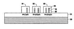
- FIG. 2Ais a schematic diagram illustrating a cross-sectional side-view diagram of a multi-fin FinFET transistor formed within a portion of an integrated circuit chip.
- FIG. 2Bis a schematic diagram of the same structure from a top-view perspective.
- the schematic diagramsillustrate a substrate 30 , an oxide 31 , multiple fins 32 , an insulator material 60 , and a gate conductor 90 formed over the fins 32 and insulator 60 .
- the fins 32 shown in FIG. 2Aextend into and out of the page and include source and drain regions 4 at their ends.
- the gate 90runs perpendicular to the fins 32 and crosses the channel regions 24 of each of the fins 32 .
- the inventioncan use more than one fin per single FinFET.
- all the sources and drains of the different finsare electrically connected to external wiring 25 so that all of the fins 32 act together when gating the conductivity between the sources and drains.
- the circuit designercan increase or decrease the channel area 24 that is exposed to, but insulated from the gate. Therefore, for fins having the same length and height, two fins would double the effective channel width when compared to a single fin, three fins would triple the effective channel width, etc.
- the inventionallows a finer granularity of channel surface area change, thereby allowing finer tuning resolution between the different circuits within a chip.
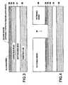
- FIGS. 3-9illustrate one method utilized by the invention by showing various manufacturing stages of the inventive structure. More specifically, FIG. 3 illustrates the use of an SOI wafer having an active (e.g., semiconducting) silicon layer 32 on top of a buried oxide layer 31 .
- Item 33represents a silicon dioxide layer in one embodiment. In another embodiment, item 33 represents a silicon dioxide with an overlying polysilicon layer.
- Item 34represents a silicon nitride layer formed over the layer 33 .
- a photoresist 40is formed and patterned over the silicon nitride layer 34 .
- the structureis then etched to remove the exposed portions 41 of the structure down to the active silicon layer 32 .
- the structureis subjected to a high temperature oxidation process. This oxidation process consumes a portion of the active silicon 32 that is exposed through the opening 41 in the resist.
- the photoresist 40is then removed. As shown in FIG. 5 , this reduces the height of the active silicon 32 in the selected region 41 . While the height of the active silicon region 32 could be reduced by continuing the etching process discussed above with respect to FIG. 4 , the oxidation process produces a much higher level of control over the height reduction in the exposed area 41 .
- the nitride 34is stripped using a selective removal process.
- layer 33included a polysilicon component, the polysilicon could also be selectively removed at this stage.
- a mask material 60is then applied and patterned in locations where the fins are to be formed.
- the oxideis etched in a selective etching process that does not affect the underlying silicon 32 .
- mask material 60is stripped and the areas of the silicon 32 that are not protected by the oxide 33 are selectively etched with respect to the oxide 31 to form the fins 32 .
- Fins 80are formed in region 41 where the height of the silicon 32 was reduced in the oxidation process (discussed above with respect to FIG.
- fins 80have a reduced height when compared to fins 81 .
- the conductive gate material 90is deposited and patterned.
- additional processingoccurs to complete the transistors. For example, the regions of the fins extending beyond the gate material 4 are doped to create source and drain regions; insulator layers are formed, contacts are formed to the gate, source, and drain, etc. In this example, three transistors 91 - 93 are formed.
- the patterned gate conductor 90is shown perpendicular to the fins containing channel regions 24 , it may be advantageous for the gate conductor to cross the fins at an angle other than ninety degrees in order to form channels on specific crystal planes.
- allowing the gate to cross fins at an angle of sixty-seven and one-half degreescan allow access to both ⁇ 110 ⁇ and ⁇ 100 ⁇ planes, to yield highest mobility of holes and electrons, respectively, in silicon.
- FIG. 10is a flow diagram which shows an embodiment of the invention.
- the inventionemploys, but is not limited to, an SOI wafer as the starting point.
- the inventionforms an oxide layer on the active silicon layer.
- the inventionpatterns a mask, or masking layers, above the oxide layer.
- the inventionperforms a thermal oxidation to reduce the height of regions of the active silicon layer not protected by the mask.
- the inventionremoves the mask, or masking layer.
- the inventionpatterns a second mask over the oxide and active silicon layer.
- the inventionpatterns the active silicon layer into fins.
- the inventionthen forms gate oxides over channel regions of the fins in item 114 .
- the inventionpatterns gate conductors over the fins so that the gate conductors cross channel regions of the fins.
- the inventiondopes portions of the fins not covered by the gate conductor to form source and drain regions in the fins.
- the inventionprovides individual control over the height of the fins of different FinFET devices within a given chip to allow tuning of the channel widths to achieve a certain performance goal.
- the inventionprovides the following methodology regarding the selection of different fin heights.
- the forgoing descriptionincludes a single high temperature oxidation process to reduce the height of a selected portion of the active silicon that will be patterned into the fins. This process could be repeated a number of different times using different masks to create three or more different fin heights (as opposed to the two fin heights discussed above). However the invention limits the need to perform a large number of high temperature oxidation processes by utilizing the fin height ratios discussed below.
- This methodologylimits the fin heights (and associated channel widths) to multiples (quanta) of a base fin height to simplify processing and allow designers the broadest range of channel width choices while maintaining reasonable manufacturing process steps.
- the finscan be spaced at a frequency no greater than approximately the lithography scale (e.g., spaced at 70 nm for 70 nm technology) because the fins are formed lithographically (as discussed above).
- Taller finswould give higher current density per unit area because fewer fins would have to be utilized to achieve a desired channel width; however, this would be at the expense of larger channel width steps (coarser granularity). Smaller fins will allow finer granularity of channel widths; however, this would consume an excessive amount of chip real-estate.
- the inventionestablishes a standard that the smaller fins will have a height of 2/3 that of the taller fins. Through experimentation, the inventors have determined that this ratio produces optimal design solution results. This solution allows a single high temperature oxidation process to be utilized (thereby maintaining high yield). Further, by forming the heights of the fins within 1/3 of each other, the processing that forms the remaining structures in the transistors does not have to be modified. To the contrary, if some fins were made dramatically smaller than others, special processes would have to be utilized to form the contacts, source, drain, oxide, etc., for the dramatically shorter fins.
- FIG. 9shows the use of the inventive one to 2/3 ratio (e.g. 1:0.667 ratio) in transistor 91 .
- the channel widthis equal to one (which, as discussed above, it is actually two times the height of the fins).
- the inventionallows FinFET devices to be tuned according to a circuit designer's needs through the use of multiple fins that can have different heights. Further, the invention establishes an optimal height ratio of one to 2/3 to allow high channel width granularity without sacrificing yield and without disturbing the conventional transistor manufacturing processes.
- the finer granularity of channel width enabled by this inventionallows those circuits whose operation is critically dependent on the relative drive strengths, or performance, of the transistors within, to occupy less physical area than would otherwise be possible. Furthermore, narrower total channel width can be achieved in these circuits, thereby resulting in lower power dissipation of the resulting circuits, when compared to conventional structures.
Landscapes
- Engineering & Computer Science (AREA)
- Physics & Mathematics (AREA)
- Condensed Matter Physics & Semiconductors (AREA)
- General Physics & Mathematics (AREA)
- Manufacturing & Machinery (AREA)
- Computer Hardware Design (AREA)
- Microelectronics & Electronic Packaging (AREA)
- Power Engineering (AREA)
- Thin Film Transistor (AREA)
- Insulated Gate Type Field-Effect Transistor (AREA)
- Metal-Oxide And Bipolar Metal-Oxide Semiconductor Integrated Circuits (AREA)
Abstract
Description
Claims (35)
Priority Applications (8)
| Application Number | Priority Date | Filing Date | Title |
|---|---|---|---|
| US10/249,738US6909147B2 (en) | 2003-05-05 | 2003-05-05 | Multi-height FinFETS |
| CNB2004800120281ACN100466229C (en) | 2003-05-05 | 2004-01-30 | Multi-height fin field effect transistor and manufacturing method thereof |
| DE602004015592TDE602004015592D1 (en) | 2003-05-05 | 2004-01-30 | METHOD FOR THE PRODUCTION OF FINFETS OF MULTIPLE HEIGHTS |
| EP04707026AEP1620891B1 (en) | 2003-05-05 | 2004-01-30 | Method of forming multi-height finfets |
| PCT/US2004/002647WO2004100290A2 (en) | 2003-05-05 | 2004-01-30 | Multi-height finfets |
| AT04707026TATE403937T1 (en) | 2003-05-05 | 2004-01-30 | METHOD OF MAKING MULTIPLE HEIGHT FINFETS |
| KR1020057018446AKR100690559B1 (en) | 2003-05-05 | 2004-01-30 | Multi-height フ INFET |
| TW093112418ATWI289354B (en) | 2003-05-05 | 2004-05-03 | Multi-height finFETs |
Applications Claiming Priority (1)
| Application Number | Priority Date | Filing Date | Title |
|---|---|---|---|
| US10/249,738US6909147B2 (en) | 2003-05-05 | 2003-05-05 | Multi-height FinFETS |
Publications (2)
| Publication Number | Publication Date |
|---|---|
| US20040222477A1 US20040222477A1 (en) | 2004-11-11 |
| US6909147B2true US6909147B2 (en) | 2005-06-21 |
Family
ID=33415537
Family Applications (1)
| Application Number | Title | Priority Date | Filing Date |
|---|---|---|---|
| US10/249,738Expired - LifetimeUS6909147B2 (en) | 2003-05-05 | 2003-05-05 | Multi-height FinFETS |
Country Status (8)
| Country | Link |
|---|---|
| US (1) | US6909147B2 (en) |
| EP (1) | EP1620891B1 (en) |
| KR (1) | KR100690559B1 (en) |
| CN (1) | CN100466229C (en) |
| AT (1) | ATE403937T1 (en) |
| DE (1) | DE602004015592D1 (en) |
| TW (1) | TWI289354B (en) |
| WO (1) | WO2004100290A2 (en) |
Cited By (69)
| Publication number | Priority date | Publication date | Assignee | Title |
|---|---|---|---|---|
| US20050215014A1 (en)* | 2004-03-23 | 2005-09-29 | Young-Joon Ahn | Complementary metal oxide semiconductor (CMOS) transistors having three-dimensional channel regions and methods of forming same |
| US20060138476A1 (en)* | 2003-06-13 | 2006-06-29 | Takefumi Nishimuta | Dc amplifier and semiconductor integrated circuit therefor |
| US20060160312A1 (en)* | 2005-01-20 | 2006-07-20 | Nirmal Chaudhary | Gate electrode for finfet device |
| US20060216880A1 (en)* | 2005-03-25 | 2006-09-28 | Hiroyuki Suto | FINFET devices and methods of fabricating FINFET devices |
| US20060281236A1 (en)* | 2003-10-02 | 2006-12-14 | Suman Datta | Method and apparatus for improving stability of a 6T CMOS SRAM cell |
| US20070075342A1 (en)* | 2005-09-30 | 2007-04-05 | Kabushiki Kaisha Toshiba | Semiconductor device with fin structure and method of manufacturing the same |
| US20070096196A1 (en)* | 2004-04-27 | 2007-05-03 | Franz Hofmann | Fin field effect transistor arrangement and method for producing a fin field effect transistor arrangement |
| US20070158764A1 (en)* | 2006-01-10 | 2007-07-12 | Freescale Semiconductor, Inc. | Electronic device including a fin-type transistor structure and a process for forming the electronic device |
| US20070161171A1 (en)* | 2006-01-10 | 2007-07-12 | Freescale Semiconductor, Inc. | Process for forming an electronic device including a fin-type structure |
| US20070158730A1 (en)* | 2006-01-10 | 2007-07-12 | Burnett James D | Integrated circuit using FinFETs and having a static random access memory (SRAM) |
| US20070218707A1 (en)* | 2006-03-15 | 2007-09-20 | Freescale Semiconductor, Inc. | Electronic device including semiconductor islands of different thicknesses over an insulating layer and a process of forming the same |
| US20070281493A1 (en)* | 2006-06-02 | 2007-12-06 | Janos Fucsko | Methods of shaping vertical single crystal silicon walls and resulting structures |
| US20070278183A1 (en)* | 2006-06-02 | 2007-12-06 | Whonchee Lee | Wet etch suitable for creating square cuts in si and resulting structures |
| US20080122013A1 (en)* | 2006-11-06 | 2008-05-29 | International Business Machines Corporation | Semiconductor structure with multiple fins having different channel region heights and method of forming the semiconductor structure |
| US20080230852A1 (en)* | 2007-03-06 | 2008-09-25 | Chen-Hua Yu | Fabrication of FinFETs with multiple fin heights |
| US20080251849A1 (en)* | 2004-03-19 | 2008-10-16 | Shigeharu Yamagami | Semiconductor Device and Method for Manufacturing Same |
| US20080265338A1 (en)* | 2007-04-27 | 2008-10-30 | Chen-Hua Yu | Semiconductor Device Having Multiple Fin Heights |
| US7456055B2 (en) | 2006-03-15 | 2008-11-25 | Freescale Semiconductor, Inc. | Process for forming an electronic device including semiconductor fins |
| US20090001470A1 (en)* | 2007-06-26 | 2009-01-01 | Anderson Brent A | Method for forming acute-angle spacer for non-orthogonal finfet and the resulting structure |
| US20090014798A1 (en)* | 2007-07-11 | 2009-01-15 | International Business Machines Corporation | Finfet sram with asymmetric gate and method of manufacture thereof |
| US20090057780A1 (en)* | 2007-08-27 | 2009-03-05 | International Business Machines Corporation | Finfet structure including multiple semiconductor fin channel heights |
| US20090057846A1 (en)* | 2007-08-30 | 2009-03-05 | Doyle Brian S | Method to fabricate adjacent silicon fins of differing heights |
| US20090209074A1 (en)* | 2008-02-19 | 2009-08-20 | Anderson Brent A | Method of forming a multi-fin multi-gate field effect transistor with tailored drive current |
| US20090206374A1 (en)* | 2008-02-19 | 2009-08-20 | Anderson Brent A | Multi-fin multi-gate field effect transistor with tailored drive current |
| US20090278196A1 (en)* | 2008-05-06 | 2009-11-12 | Cheng-Hung Chang | FinFETs having dielectric punch-through stoppers |
| US7625776B2 (en) | 2006-06-02 | 2009-12-01 | Micron Technology, Inc. | Methods of fabricating intermediate semiconductor structures by selectively etching pockets of implanted silicon |
| US20100112770A1 (en)* | 2008-11-06 | 2010-05-06 | Nec Electronics Corporation | Semiconductor device and method of manufacturing semiconductor device |
| US20100144121A1 (en)* | 2008-12-05 | 2010-06-10 | Cheng-Hung Chang | Germanium FinFETs Having Dielectric Punch-Through Stoppers |
| US7736956B2 (en) | 2005-08-17 | 2010-06-15 | Intel Corporation | Lateral undercut of metal gate in SOI device |
| US20100163971A1 (en)* | 2008-12-31 | 2010-07-01 | Shih-Ting Hung | Dielectric Punch-Through Stoppers for Forming FinFETs Having Dual Fin Heights |
| US20100213548A1 (en)* | 2009-02-24 | 2010-08-26 | Cheng-Hung Chang | Semiconductor Devices with Low Junction Capacitances and Methods of Fabrication Thereof |
| US7855105B1 (en)* | 2009-06-18 | 2010-12-21 | International Business Machines Corporation | Planar and non-planar CMOS devices with multiple tuned threshold voltages |
| US20100327261A1 (en)* | 2007-08-30 | 2010-12-30 | Intel Corporation | High hole mobility p-channel ge transistor structure on si substrate |
| US20110042748A1 (en)* | 2009-08-18 | 2011-02-24 | International Business Machines Corporation | Multi-gate non-planar field effect transistor structure and method of forming the structure using a dopant implant process to tune device drive current |
| US7898041B2 (en) | 2005-06-30 | 2011-03-01 | Intel Corporation | Block contact architectures for nanoscale channel transistors |
| US7915167B2 (en) | 2004-09-29 | 2011-03-29 | Intel Corporation | Fabrication of channel wraparound gate structure for field-effect transistor |
| US20110129978A1 (en)* | 2009-12-01 | 2011-06-02 | Kangguo Cheng | Method and structure for forming finfets with multiple doping regions on a same chip |
| US7960794B2 (en) | 2004-08-10 | 2011-06-14 | Intel Corporation | Non-planar pMOS structure with a strained channel region and an integrated strained CMOS flow |
| US20110147848A1 (en)* | 2009-12-23 | 2011-06-23 | Kuhn Kelin J | Multiple transistor fin heights |
| US8067818B2 (en) | 2004-10-25 | 2011-11-29 | Intel Corporation | Nonplanar device with thinned lower body portion and method of fabrication |
| US8071983B2 (en) | 2005-06-21 | 2011-12-06 | Intel Corporation | Semiconductor device structures and methods of forming semiconductor structures |
| US8084818B2 (en) | 2004-06-30 | 2011-12-27 | Intel Corporation | High mobility tri-gate devices and methods of fabrication |
| US8183646B2 (en) | 2005-02-23 | 2012-05-22 | Intel Corporation | Field effect transistor with narrow bandgap source and drain regions and method of fabrication |
| US8193567B2 (en) | 2005-09-28 | 2012-06-05 | Intel Corporation | Process for integrating planar and non-planar CMOS transistors on a bulk substrate and article made thereby |
| US8268709B2 (en) | 2004-09-29 | 2012-09-18 | Intel Corporation | Independently accessed double-gate and tri-gate transistors in same process flow |
| US8273626B2 (en) | 2003-06-27 | 2012-09-25 | Intel Corporationn | Nonplanar semiconductor device with partially or fully wrapped around gate electrode and methods of fabrication |
| US8294180B2 (en) | 2005-09-28 | 2012-10-23 | Intel Corporation | CMOS devices with a single work function gate electrode and method of fabrication |
| US8362566B2 (en) | 2008-06-23 | 2013-01-29 | Intel Corporation | Stress in trigate devices using complimentary gate fill materials |
| US8405164B2 (en) | 2003-06-27 | 2013-03-26 | Intel Corporation | Tri-gate transistor device with stress incorporation layer and method of fabrication |
| US8524545B2 (en) | 2010-10-22 | 2013-09-03 | International Business Machines Corporation | Simultaneous formation of FinFET and MUGFET |
| US8524546B2 (en) | 2010-10-22 | 2013-09-03 | International Business Machines Corporation | Formation of multi-height MUGFET |
| US8809178B2 (en) | 2012-02-29 | 2014-08-19 | Globalfoundries Inc. | Methods of forming bulk FinFET devices with replacement gates so as to reduce punch through leakage currents |
| US8987100B2 (en) | 2012-03-19 | 2015-03-24 | Samsung Electronics Co., Ltd. | Method of fabricating fin-field effect transistors (finfets) having different fin widths |
| US9082873B2 (en) | 2012-09-20 | 2015-07-14 | International Business Machines Corporation | Method and structure for finFET with finely controlled device width |
| US9093275B2 (en) | 2013-10-22 | 2015-07-28 | International Business Machines Corporation | Multi-height multi-composition semiconductor fins |
| US9105723B2 (en) | 2013-05-31 | 2015-08-11 | International Business Machines Corporation | Multi-height FinFETs with coplanar topography |
| US9159576B2 (en) | 2013-03-05 | 2015-10-13 | Qualcomm Incorporated | Method of forming finFET having fins of different height |
| US9190466B2 (en) | 2013-12-27 | 2015-11-17 | International Business Machines Corporation | Independent gate vertical FinFET structure |
| US9337307B2 (en) | 2005-06-15 | 2016-05-10 | Intel Corporation | Method for fabricating transistor with thinned channel |
| US9564435B2 (en) | 2014-10-13 | 2017-02-07 | Samsung Electronics Co., Ltd. | Semiconductor device including FinFETs having different gate structures and method of manufacturing the semiconductor device |
| US9577066B1 (en) | 2016-02-26 | 2017-02-21 | Globalfoundries Inc. | Methods of forming fins with different fin heights |
| US9691763B2 (en) | 2013-12-27 | 2017-06-27 | International Business Machines Corporation | Multi-gate FinFET semiconductor device with flexible design width |
| US9887196B2 (en) | 2014-04-07 | 2018-02-06 | International Business Machines Corporation | FinFET including tunable fin height and tunable fin width ratio |
| US10068902B1 (en) | 2017-09-26 | 2018-09-04 | Globalfoundries Inc. | Integrated circuit structure incorporating non-planar field effect transistors with different channel region heights and method |
| DE102017125352A1 (en)* | 2017-08-30 | 2019-02-28 | Taiwan Semiconductor Manufacturing Co., Ltd. | RIB STRUCTURE FOR A SEMICONDUCTOR DEVICE |
| US20190131177A1 (en)* | 2017-10-26 | 2019-05-02 | Globalfoundries Inc. | Field-effect transistors with fins having independently-dimensioned sections |
| US10297667B1 (en) | 2017-12-22 | 2019-05-21 | International Business Machines Corporation | Fin field-effect transistor for input/output device integrated with nanosheet field-effect transistor |
| US10541319B2 (en) | 2017-08-30 | 2020-01-21 | Taiwan Semiconductor Manufacturing Co., Ltd. | Fin structures having varied fin heights for semiconductor device |
| US11417531B2 (en)* | 2013-12-23 | 2022-08-16 | Intel Corporation | Advanced etching technologies for straight, tall and uniform fins across multiple fin pitch structures |
Families Citing this family (38)
| Publication number | Priority date | Publication date | Assignee | Title |
|---|---|---|---|---|
| US6992354B2 (en)* | 2003-06-25 | 2006-01-31 | International Business Machines Corporation | FinFET having suppressed parasitic device characteristics |
| US6894326B2 (en)* | 2003-06-25 | 2005-05-17 | International Business Machines Corporation | High-density finFET integration scheme |
| US7095065B2 (en)* | 2003-08-05 | 2006-08-22 | Advanced Micro Devices, Inc. | Varying carrier mobility in semiconductor devices to achieve overall design goals |
| JP2005086024A (en)* | 2003-09-09 | 2005-03-31 | Toshiba Corp | Semiconductor device and method for manufacturing same |
| US7183142B2 (en)* | 2005-01-13 | 2007-02-27 | International Business Machines Corporation | FinFETs with long gate length at high density |
| US7470951B2 (en)* | 2005-01-31 | 2008-12-30 | Freescale Semiconductor, Inc. | Hybrid-FET and its application as SRAM |
| US7452768B2 (en) | 2005-10-25 | 2008-11-18 | Freescale Semiconductor, Inc. | Multiple device types including an inverted-T channel transistor and method therefor |
| US8513066B2 (en)* | 2005-10-25 | 2013-08-20 | Freescale Semiconductor, Inc. | Method of making an inverted-T channel transistor |
| US20070117311A1 (en)* | 2005-11-23 | 2007-05-24 | Advanced Technology Development Facility, Inc. | Three-dimensional single transistor semiconductor memory device and methods for making same |
| US7323373B2 (en)* | 2006-01-25 | 2008-01-29 | Freescale Semiconductor, Inc. | Method of forming a semiconductor device with decreased undercutting of semiconductor material |
| US7655989B2 (en)* | 2006-11-30 | 2010-02-02 | International Business Machines Corporation | Triple gate and double gate finFETs with different vertical dimension fins |
| US7709893B2 (en)* | 2007-01-31 | 2010-05-04 | Infineon Technologies Ag | Circuit layout for different performance and method |
| CN100527442C (en)* | 2007-06-05 | 2009-08-12 | 北京大学 | Double-fin type channel double-grid multifunction field effect transistor and producing method thereof |
| US7859044B2 (en)* | 2007-07-24 | 2010-12-28 | International Business Machines Corporation | Partially gated FINFET with gate dielectric on only one sidewall |
| US7710765B2 (en)* | 2007-09-27 | 2010-05-04 | Micron Technology, Inc. | Back gated SRAM cell |
| US20090321834A1 (en)* | 2008-06-30 | 2009-12-31 | Willy Rachmady | Substrate fins with different heights |
| CN103022038B (en)* | 2011-09-21 | 2015-06-10 | 中国科学院微电子研究所 | Sram unit and manufacturing method thereof |
| US8497198B2 (en)* | 2011-09-23 | 2013-07-30 | United Microelectronics Corp. | Semiconductor process |
| CN103187284B (en)* | 2011-12-29 | 2015-10-14 | 中芯国际集成电路制造(上海)有限公司 | The manufacture method of field-effect transistor |
| US8927432B2 (en)* | 2012-06-14 | 2015-01-06 | International Business Machines Corporation | Continuously scalable width and height semiconductor fins |
| US9583398B2 (en)* | 2012-06-29 | 2017-02-28 | Taiwan Semiconductor Manufacturing Company, Ltd. | Integrated circuit having FinFETS with different fin profiles |
| CN103811340B (en)* | 2012-11-09 | 2017-07-14 | 中国科学院微电子研究所 | Semiconductor device and method for manufacturing the same |
| US9123654B2 (en)* | 2013-02-15 | 2015-09-01 | International Business Machines Corporation | Trilayer SIT process with transfer layer for FINFET patterning |
| TWI570812B (en)* | 2013-03-06 | 2017-02-11 | 聯華電子股份有限公司 | Method for forming fin-shaped structure |
| US9293466B2 (en) | 2013-06-19 | 2016-03-22 | Taiwan Semiconductor Manufacturing Company, Ltd. | Embedded SRAM and methods of forming the same |
| CN104253046B (en)* | 2013-06-26 | 2016-12-28 | 中芯国际集成电路制造(上海)有限公司 | Fin formula field effect transistor and forming method thereof |
| US9704880B2 (en)* | 2013-11-06 | 2017-07-11 | Taiwan Semiconductor Manufacturing Company Limited | Systems and methods for a semiconductor structure having multiple semiconductor-device layers |
| US9318488B2 (en) | 2014-01-06 | 2016-04-19 | Taiwan Semiconductor Manufacturing Company Limited | Semiconductor device and formation thereof |
| US20150287743A1 (en) | 2014-04-02 | 2015-10-08 | International Business Machines Corporation | Multi-height fin field effect transistors |
| US9418903B2 (en) | 2014-05-21 | 2016-08-16 | Globalfoundries Inc. | Structure and method for effective device width adjustment in finFET devices using gate workfunction shift |
| US9793269B2 (en) | 2014-08-07 | 2017-10-17 | Taiwan Semiconductor Manufacturing Company, Ltd. | Semiconductor device and method of manufacture |
| KR102352154B1 (en)* | 2015-03-03 | 2022-01-17 | 삼성전자주식회사 | Integrated circuit device |
| US9515089B1 (en)* | 2015-05-14 | 2016-12-06 | International Business Machines Corporation | Bulk fin formation with vertical fin sidewall profile |
| US10707346B2 (en)* | 2015-09-25 | 2020-07-07 | Intel Corporation | High-voltage transistor with self-aligned isolation |
| US10593598B2 (en)* | 2017-12-23 | 2020-03-17 | International Business Machines Corporation | Vertical FET with various gate lengths by an oxidation process |
| US11257928B2 (en)* | 2018-11-27 | 2022-02-22 | Taiwan Semiconductor Manufacturing Company, Ltd. | Method for epitaxial growth and device |
| US11011517B2 (en) | 2019-01-02 | 2021-05-18 | International Business Machines Corporation | Semiconductor structure including first FinFET devices for low power applications and second FinFET devices for high power applications |
| EP4120333A4 (en)* | 2021-04-28 | 2023-10-25 | Changxin Memory Technologies, Inc. | METHOD FOR PRODUCING A SEMICONDUCTOR STRUCTURE |
Citations (10)
| Publication number | Priority date | Publication date | Assignee | Title |
|---|---|---|---|---|
| US4996574A (en)* | 1988-07-01 | 1991-02-26 | Fujitsu Limited | MIS transistor structure for increasing conductance between source and drain regions |
| US6252284B1 (en) | 1999-12-09 | 2001-06-26 | International Business Machines Corporation | Planarized silicon fin device |
| US6413802B1 (en)* | 2000-10-23 | 2002-07-02 | The Regents Of The University Of California | Finfet transistor structures having a double gate channel extending vertically from a substrate and methods of manufacture |
| US6562665B1 (en)* | 2000-10-16 | 2003-05-13 | Advanced Micro Devices, Inc. | Fabrication of a field effect transistor with a recess in a semiconductor pillar in SOI technology |
| US6645797B1 (en)* | 2002-12-06 | 2003-11-11 | Advanced Micro Devices, Inc. | Method for forming fins in a FinFET device using sacrificial carbon layer |
| US6657259B2 (en)* | 2001-12-04 | 2003-12-02 | International Business Machines Corporation | Multiple-plane FinFET CMOS |
| US6706571B1 (en)* | 2002-10-22 | 2004-03-16 | Advanced Micro Devices, Inc. | Method for forming multiple structures in a semiconductor device |
| US20040099885A1 (en)* | 2002-11-26 | 2004-05-27 | Taiwan Semiconductor Manufacturing Co., Ltd. | CMOS SRAM cell configured using multiple-gate transistors |
| US20040110331A1 (en)* | 2002-12-06 | 2004-06-10 | Yee-Chia Yeo | CMOS inverters configured using multiple-gate transistors |
| US6762448B1 (en)* | 2003-04-03 | 2004-07-13 | Advanced Micro Devices, Inc. | FinFET device with multiple fin structures |
Family Cites Families (4)
| Publication number | Priority date | Publication date | Assignee | Title |
|---|---|---|---|---|
| US6288431B1 (en)* | 1997-04-04 | 2001-09-11 | Nippon Steel Corporation | Semiconductor device and a method of manufacturing the same |
| EP1091413A3 (en)* | 1999-10-06 | 2005-01-12 | Lsi Logic Corporation | Fully-depleted, fully-inverted, short-length and vertical channel, dual-gate, cmos fet |
| US20020011612A1 (en)* | 2000-07-31 | 2002-01-31 | Kabushiki Kaisha Toshiba | Semiconductor device and method for manufacturing the same |
| JP4044276B2 (en)* | 2000-09-28 | 2008-02-06 | 株式会社東芝 | Semiconductor device and manufacturing method thereof |
- 2003
- 2003-05-05USUS10/249,738patent/US6909147B2/ennot_activeExpired - Lifetime
- 2004
- 2004-01-30KRKR1020057018446Apatent/KR100690559B1/ennot_activeExpired - Fee Related
- 2004-01-30DEDE602004015592Tpatent/DE602004015592D1/ennot_activeExpired - Lifetime
- 2004-01-30ATAT04707026Tpatent/ATE403937T1/ennot_activeIP Right Cessation
- 2004-01-30CNCNB2004800120281Apatent/CN100466229C/ennot_activeExpired - Fee Related
- 2004-01-30EPEP04707026Apatent/EP1620891B1/ennot_activeExpired - Lifetime
- 2004-01-30WOPCT/US2004/002647patent/WO2004100290A2/enactiveSearch and Examination
- 2004-05-03TWTW093112418Apatent/TWI289354B/ennot_activeIP Right Cessation
Patent Citations (11)
| Publication number | Priority date | Publication date | Assignee | Title |
|---|---|---|---|---|
| US4996574A (en)* | 1988-07-01 | 1991-02-26 | Fujitsu Limited | MIS transistor structure for increasing conductance between source and drain regions |
| US6252284B1 (en) | 1999-12-09 | 2001-06-26 | International Business Machines Corporation | Planarized silicon fin device |
| US20010036731A1 (en)* | 1999-12-09 | 2001-11-01 | Muller K. Paul L. | Process for making planarized silicon fin device |
| US6562665B1 (en)* | 2000-10-16 | 2003-05-13 | Advanced Micro Devices, Inc. | Fabrication of a field effect transistor with a recess in a semiconductor pillar in SOI technology |
| US6413802B1 (en)* | 2000-10-23 | 2002-07-02 | The Regents Of The University Of California | Finfet transistor structures having a double gate channel extending vertically from a substrate and methods of manufacture |
| US6657259B2 (en)* | 2001-12-04 | 2003-12-02 | International Business Machines Corporation | Multiple-plane FinFET CMOS |
| US6706571B1 (en)* | 2002-10-22 | 2004-03-16 | Advanced Micro Devices, Inc. | Method for forming multiple structures in a semiconductor device |
| US20040099885A1 (en)* | 2002-11-26 | 2004-05-27 | Taiwan Semiconductor Manufacturing Co., Ltd. | CMOS SRAM cell configured using multiple-gate transistors |
| US6645797B1 (en)* | 2002-12-06 | 2003-11-11 | Advanced Micro Devices, Inc. | Method for forming fins in a FinFET device using sacrificial carbon layer |
| US20040110331A1 (en)* | 2002-12-06 | 2004-06-10 | Yee-Chia Yeo | CMOS inverters configured using multiple-gate transistors |
| US6762448B1 (en)* | 2003-04-03 | 2004-07-13 | Advanced Micro Devices, Inc. | FinFET device with multiple fin structures |
Non-Patent Citations (3)
| Title |
|---|
| Huang, Xuejue et al. "Sub-50nm P-Channel FinFET" May 2001. IEEE Transactions on Electron Devices, vol. 48, No. 5. pp 880-886.* |
| Kedzierski, Jakub et al., "High-performance symmetric-gate and CMOS-compatible Vt asymmetric-gate FinFET devices," Dec. 2001. Electron Devices Meeting, 2001, IEDM Technical Digest, pp 19.5.1-19.5.4.* |
| Pei, Gen et al. "FinFET Design Considerations Based on 3-D Simulation and analytical Modeling" Aug. 2002. IEEE Transactions on Electron Devices, vol. 49, No. 8., pp 1411-1419.* |
Cited By (171)
| Publication number | Priority date | Publication date | Assignee | Title |
|---|---|---|---|---|
| US20060138476A1 (en)* | 2003-06-13 | 2006-06-29 | Takefumi Nishimuta | Dc amplifier and semiconductor integrated circuit therefor |
| US8405164B2 (en) | 2003-06-27 | 2013-03-26 | Intel Corporation | Tri-gate transistor device with stress incorporation layer and method of fabrication |
| US8273626B2 (en) | 2003-06-27 | 2012-09-25 | Intel Corporationn | Nonplanar semiconductor device with partially or fully wrapped around gate electrode and methods of fabrication |
| US7445980B2 (en)* | 2003-10-02 | 2008-11-04 | Intel Corporation | Method and apparatus for improving stability of a 6T CMOS SRAM cell |
| US20060281236A1 (en)* | 2003-10-02 | 2006-12-14 | Suman Datta | Method and apparatus for improving stability of a 6T CMOS SRAM cell |
| US20080251849A1 (en)* | 2004-03-19 | 2008-10-16 | Shigeharu Yamagami | Semiconductor Device and Method for Manufacturing Same |
| US7701018B2 (en)* | 2004-03-19 | 2010-04-20 | Nec Corporation | Semiconductor device and method for manufacturing same |
| US20050215014A1 (en)* | 2004-03-23 | 2005-09-29 | Young-Joon Ahn | Complementary metal oxide semiconductor (CMOS) transistors having three-dimensional channel regions and methods of forming same |
| US7384850B2 (en)* | 2004-03-23 | 2008-06-10 | Samsung Electronics Co., Ltd. | Methods of forming complementary metal oxide semiconductor (CMOS) transistors having three-dimensional channel regions therein |
| US7719059B2 (en)* | 2004-04-27 | 2010-05-18 | Infineon Technologies Ag | Fin field effect transistor arrangement and method for producing a fin field effect transistor arrangement |
| US20070096196A1 (en)* | 2004-04-27 | 2007-05-03 | Franz Hofmann | Fin field effect transistor arrangement and method for producing a fin field effect transistor arrangement |
| US8084818B2 (en) | 2004-06-30 | 2011-12-27 | Intel Corporation | High mobility tri-gate devices and methods of fabrication |
| US7960794B2 (en) | 2004-08-10 | 2011-06-14 | Intel Corporation | Non-planar pMOS structure with a strained channel region and an integrated strained CMOS flow |
| US7915167B2 (en) | 2004-09-29 | 2011-03-29 | Intel Corporation | Fabrication of channel wraparound gate structure for field-effect transistor |
| US8399922B2 (en) | 2004-09-29 | 2013-03-19 | Intel Corporation | Independently accessed double-gate and tri-gate transistors |
| US8268709B2 (en) | 2004-09-29 | 2012-09-18 | Intel Corporation | Independently accessed double-gate and tri-gate transistors in same process flow |
| US8502351B2 (en) | 2004-10-25 | 2013-08-06 | Intel Corporation | Nonplanar device with thinned lower body portion and method of fabrication |
| US10236356B2 (en) | 2004-10-25 | 2019-03-19 | Intel Corporation | Nonplanar device with thinned lower body portion and method of fabrication |
| US8067818B2 (en) | 2004-10-25 | 2011-11-29 | Intel Corporation | Nonplanar device with thinned lower body portion and method of fabrication |
| US9741809B2 (en) | 2004-10-25 | 2017-08-22 | Intel Corporation | Nonplanar device with thinned lower body portion and method of fabrication |
| US9190518B2 (en) | 2004-10-25 | 2015-11-17 | Intel Corporation | Nonplanar device with thinned lower body portion and method of fabrication |
| US8749026B2 (en) | 2004-10-25 | 2014-06-10 | Intel Corporation | Nonplanar device with thinned lower body portion and method of fabrication |
| US7094650B2 (en)* | 2005-01-20 | 2006-08-22 | Infineon Technologies Ag | Gate electrode for FinFET device |
| US20060160312A1 (en)* | 2005-01-20 | 2006-07-20 | Nirmal Chaudhary | Gate electrode for finfet device |
| US8816394B2 (en) | 2005-02-23 | 2014-08-26 | Intel Corporation | Field effect transistor with narrow bandgap source and drain regions and method of fabrication |
| US10121897B2 (en) | 2005-02-23 | 2018-11-06 | Intel Corporation | Field effect transistor with narrow bandgap source and drain regions and method of fabrication |
| US9048314B2 (en) | 2005-02-23 | 2015-06-02 | Intel Corporation | Field effect transistor with narrow bandgap source and drain regions and method of fabrication |
| US8664694B2 (en) | 2005-02-23 | 2014-03-04 | Intel Corporation | Field effect transistor with narrow bandgap source and drain regions and method of fabrication |
| US8183646B2 (en) | 2005-02-23 | 2012-05-22 | Intel Corporation | Field effect transistor with narrow bandgap source and drain regions and method of fabrication |
| US9368583B2 (en) | 2005-02-23 | 2016-06-14 | Intel Corporation | Field effect transistor with narrow bandgap source and drain regions and method of fabrication |
| US9614083B2 (en) | 2005-02-23 | 2017-04-04 | Intel Corporation | Field effect transistor with narrow bandgap source and drain regions and method of fabrication |
| US8368135B2 (en) | 2005-02-23 | 2013-02-05 | Intel Corporation | Field effect transistor with narrow bandgap source and drain regions and method of fabrication |
| US9748391B2 (en) | 2005-02-23 | 2017-08-29 | Intel Corporation | Field effect transistor with narrow bandgap source and drain regions and method of fabrication |
| US20060216880A1 (en)* | 2005-03-25 | 2006-09-28 | Hiroyuki Suto | FINFET devices and methods of fabricating FINFET devices |
| US9806195B2 (en) | 2005-06-15 | 2017-10-31 | Intel Corporation | Method for fabricating transistor with thinned channel |
| US9337307B2 (en) | 2005-06-15 | 2016-05-10 | Intel Corporation | Method for fabricating transistor with thinned channel |
| US11978799B2 (en) | 2005-06-15 | 2024-05-07 | Tahoe Research, Ltd. | Method for fabricating transistor with thinned channel |
| US8581258B2 (en) | 2005-06-21 | 2013-11-12 | Intel Corporation | Semiconductor device structures and methods of forming semiconductor structures |
| US8933458B2 (en) | 2005-06-21 | 2015-01-13 | Intel Corporation | Semiconductor device structures and methods of forming semiconductor structures |
| US8071983B2 (en) | 2005-06-21 | 2011-12-06 | Intel Corporation | Semiconductor device structures and methods of forming semiconductor structures |
| US9385180B2 (en) | 2005-06-21 | 2016-07-05 | Intel Corporation | Semiconductor device structures and methods of forming semiconductor structures |
| US9761724B2 (en) | 2005-06-21 | 2017-09-12 | Intel Corporation | Semiconductor device structures and methods of forming semiconductor structures |
| US7898041B2 (en) | 2005-06-30 | 2011-03-01 | Intel Corporation | Block contact architectures for nanoscale channel transistors |
| US7736956B2 (en) | 2005-08-17 | 2010-06-15 | Intel Corporation | Lateral undercut of metal gate in SOI device |
| US8294180B2 (en) | 2005-09-28 | 2012-10-23 | Intel Corporation | CMOS devices with a single work function gate electrode and method of fabrication |
| US8193567B2 (en) | 2005-09-28 | 2012-06-05 | Intel Corporation | Process for integrating planar and non-planar CMOS transistors on a bulk substrate and article made thereby |
| US20070075342A1 (en)* | 2005-09-30 | 2007-04-05 | Kabushiki Kaisha Toshiba | Semiconductor device with fin structure and method of manufacturing the same |
| US7709303B2 (en) | 2006-01-10 | 2010-05-04 | Freescale Semiconductor, Inc. | Process for forming an electronic device including a fin-type structure |
| US8088657B2 (en)* | 2006-01-10 | 2012-01-03 | Freescale Semiconductor, Inc. | Integrated circuit using FinFETs and having a static random access memory (SRAM) |
| US7723805B2 (en) | 2006-01-10 | 2010-05-25 | Freescale Semiconductor, Inc. | Electronic device including a fin-type transistor structure and a process for forming the electronic device |
| TWI397961B (en)* | 2006-01-10 | 2013-06-01 | Freescale Semiconductor Inc | Process for forming an electronic device including a fin structure |
| US20070158764A1 (en)* | 2006-01-10 | 2007-07-12 | Freescale Semiconductor, Inc. | Electronic device including a fin-type transistor structure and a process for forming the electronic device |
| US7754560B2 (en)* | 2006-01-10 | 2010-07-13 | Freescale Semiconductor, Inc. | Integrated circuit using FinFETs and having a static random access memory (SRAM) |
| US20100190308A1 (en)* | 2006-01-10 | 2010-07-29 | Freescale Semiconductor, Inc. | Electronic device including a fin-type transistor structure and a process for forming the electronic device |
| US7939412B2 (en) | 2006-01-10 | 2011-05-10 | Freescale Semiconductor, Inc. | Process for forming an electronic device including a fin-type transistor structure |
| US20070161171A1 (en)* | 2006-01-10 | 2007-07-12 | Freescale Semiconductor, Inc. | Process for forming an electronic device including a fin-type structure |
| US20100230762A1 (en)* | 2006-01-10 | 2010-09-16 | Freescale Semiconductor, Inc. | integrated circuit using finfets and having a static random access memory (sram) |
| WO2007120293A3 (en)* | 2006-01-10 | 2008-11-06 | Freescale Semiconductor Inc | Process for forming an electronic device including a fin-type structure |
| US20070158730A1 (en)* | 2006-01-10 | 2007-07-12 | Burnett James D | Integrated circuit using FinFETs and having a static random access memory (SRAM) |
| US20070218707A1 (en)* | 2006-03-15 | 2007-09-20 | Freescale Semiconductor, Inc. | Electronic device including semiconductor islands of different thicknesses over an insulating layer and a process of forming the same |
| US7456055B2 (en) | 2006-03-15 | 2008-11-25 | Freescale Semiconductor, Inc. | Process for forming an electronic device including semiconductor fins |
| US7419866B2 (en) | 2006-03-15 | 2008-09-02 | Freescale Semiconductor, Inc. | Process of forming an electronic device including a semiconductor island over an insulating layer |
| US7709341B2 (en) | 2006-06-02 | 2010-05-04 | Micron Technology, Inc. | Methods of shaping vertical single crystal silicon walls and resulting structures |
| US9040424B2 (en) | 2006-06-02 | 2015-05-26 | Micron Technology, Inc. | Methods of forming single crystal silicon structures and semiconductor device structures including single crystal silicon structures |
| US7625776B2 (en) | 2006-06-02 | 2009-12-01 | Micron Technology, Inc. | Methods of fabricating intermediate semiconductor structures by selectively etching pockets of implanted silicon |
| US8664742B2 (en) | 2006-06-02 | 2014-03-04 | Micron Technology, Inc. | Semiconductor substrates with undercut structures |
| US8450214B2 (en) | 2006-06-02 | 2013-05-28 | Micron Technology, Inc. | Methods of etching single crystal silicon |
| US20100109120A1 (en)* | 2006-06-02 | 2010-05-06 | Micron Technology, Inc. | Single crystal silicon structures |
| US20070278183A1 (en)* | 2006-06-02 | 2007-12-06 | Whonchee Lee | Wet etch suitable for creating square cuts in si and resulting structures |
| US7628932B2 (en) | 2006-06-02 | 2009-12-08 | Micron Technology, Inc. | Wet etch suitable for creating square cuts in si |
| US8294246B2 (en) | 2006-06-02 | 2012-10-23 | Micron Technology, Inc. | Semiconductor structures including square cuts in single crystal silicon and method of forming same |
| US20100013061A1 (en)* | 2006-06-02 | 2010-01-21 | Micron Technology, Inc. | Semiconductor structures including square cuts in single crystal silicon |
| US7973388B2 (en) | 2006-06-02 | 2011-07-05 | Micron Technology, Inc. | Semiconductor structures including square cuts in single crystal silicon |
| US20070281493A1 (en)* | 2006-06-02 | 2007-12-06 | Janos Fucsko | Methods of shaping vertical single crystal silicon walls and resulting structures |
| US20100065941A1 (en)* | 2006-06-02 | 2010-03-18 | Micron Technology, Inc. | Intermediate semiconductor structures |
| US8159050B2 (en) | 2006-06-02 | 2012-04-17 | Micron Technology, Inc. | Single crystal silicon structures |
| US7544994B2 (en) | 2006-11-06 | 2009-06-09 | International Business Machines Corporation | Semiconductor structure with multiple fins having different channel region heights and method of forming the semiconductor structure |
| US7781273B2 (en) | 2006-11-06 | 2010-08-24 | International Business Machines Corporation | Semiconductor structure with multiple fins having different channel region heights and method of forming the semiconductor structure |
| US20080224258A1 (en)* | 2006-11-06 | 2008-09-18 | International Business Machines Corporation | Semiconductor structue with multiple fins having different channel region heights and method of forming the semiconductor structure |
| US20080122013A1 (en)* | 2006-11-06 | 2008-05-29 | International Business Machines Corporation | Semiconductor structure with multiple fins having different channel region heights and method of forming the semiconductor structure |
| US7612405B2 (en) | 2007-03-06 | 2009-11-03 | Taiwan Semiconductor Manufacturing Company, Ltd. | Fabrication of FinFETs with multiple fin heights |
| US20080230852A1 (en)* | 2007-03-06 | 2008-09-25 | Chen-Hua Yu | Fabrication of FinFETs with multiple fin heights |
| US7560785B2 (en) | 2007-04-27 | 2009-07-14 | Taiwan Semiconductor Manufacturing Company, Ltd. | Semiconductor device having multiple fin heights |
| US8101994B2 (en) | 2007-04-27 | 2012-01-24 | Taiwan Semiconductor Manufacturing Company, Ltd. | Semiconductor device having multiple fin heights |
| US7843000B2 (en) | 2007-04-27 | 2010-11-30 | Taiwan Semiconductor Manufacturing Company, Ltd. | Semiconductor device having multiple fin heights |
| US20080265338A1 (en)* | 2007-04-27 | 2008-10-30 | Chen-Hua Yu | Semiconductor Device Having Multiple Fin Heights |
| US20090250769A1 (en)* | 2007-04-27 | 2009-10-08 | Chen-Hua Yu | Semiconductor Device Having Multiple Fin Heights |
| US20090253266A1 (en)* | 2007-04-27 | 2009-10-08 | Chen-Hua Yu | Semiconductor Device Having Multiple Fin Heights |
| US20110037129A1 (en)* | 2007-04-27 | 2011-02-17 | Taiwan Semiconductor Manufacturing Company, Ltd. | Semiconductor Device Having Multiple Fin Heights |
| US7902035B2 (en) | 2007-04-27 | 2011-03-08 | Taiwan Semiconductor Manufacturing Company, Ltd. | Semiconductor device having multiple fin heights |
| US20090001470A1 (en)* | 2007-06-26 | 2009-01-01 | Anderson Brent A | Method for forming acute-angle spacer for non-orthogonal finfet and the resulting structure |
| US20090014798A1 (en)* | 2007-07-11 | 2009-01-15 | International Business Machines Corporation | Finfet sram with asymmetric gate and method of manufacture thereof |
| US7737501B2 (en) | 2007-07-11 | 2010-06-15 | International Business Machines Corporation | FinFET SRAM with asymmetric gate and method of manufacture thereof |
| US20090057780A1 (en)* | 2007-08-27 | 2009-03-05 | International Business Machines Corporation | Finfet structure including multiple semiconductor fin channel heights |
| WO2009032576A3 (en)* | 2007-08-30 | 2009-05-07 | Intel Corp | Method to fabricate adjacent silicon fins of differing heights |
| KR101248339B1 (en)* | 2007-08-30 | 2013-04-01 | 인텔 코오퍼레이션 | Method to fabricate adjacent silicon fins of differing heights |
| US20100327261A1 (en)* | 2007-08-30 | 2010-12-30 | Intel Corporation | High hole mobility p-channel ge transistor structure on si substrate |
| US20090057846A1 (en)* | 2007-08-30 | 2009-03-05 | Doyle Brian S | Method to fabricate adjacent silicon fins of differing heights |
| US8217383B2 (en) | 2007-08-30 | 2012-07-10 | Intel Corporation | High hole mobility p-channel Ge transistor structure on Si substrate |
| US20090206374A1 (en)* | 2008-02-19 | 2009-08-20 | Anderson Brent A | Multi-fin multi-gate field effect transistor with tailored drive current |
| US20090209074A1 (en)* | 2008-02-19 | 2009-08-20 | Anderson Brent A | Method of forming a multi-fin multi-gate field effect transistor with tailored drive current |
| US7888750B2 (en) | 2008-02-19 | 2011-02-15 | International Business Machines Corporation | Multi-fin multi-gate field effect transistor with tailored drive current |
| US8022478B2 (en) | 2008-02-19 | 2011-09-20 | International Business Machines Corporation | Method of forming a multi-fin multi-gate field effect transistor with tailored drive current |
| US10312327B2 (en) | 2008-05-06 | 2019-06-04 | Taiwan Semiconductor Manufacturing Company, Ltd. | FinFETs having dielectric punch-through stoppers |
| US9722025B2 (en) | 2008-05-06 | 2017-08-01 | Taiwan Semiconductor Manufacturing Company, Ltd. | FinFETs having dielectric punch-through stoppers |
| US9230959B2 (en) | 2008-05-06 | 2016-01-05 | Taiwan Semiconductor Manufacturing Company, Ltd. | FinFETs having dielectric punch-through stoppers |
| US8957477B2 (en) | 2008-05-06 | 2015-02-17 | Taiwan Semiconductor Manufacturing Company, Ltd. | Germanium FinFETs having dielectric punch-through stoppers |
| US20090278196A1 (en)* | 2008-05-06 | 2009-11-12 | Cheng-Hung Chang | FinFETs having dielectric punch-through stoppers |
| US8106459B2 (en)* | 2008-05-06 | 2012-01-31 | Taiwan Semiconductor Manufacturing Company, Ltd. | FinFETs having dielectric punch-through stoppers |
| US11133387B2 (en) | 2008-05-06 | 2021-09-28 | Taiwan Semiconductor Manufacturing Company, Ltd. | FinFETs having dielectric punch-through stoppers |
| US9450092B2 (en) | 2008-06-23 | 2016-09-20 | Intel Corporation | Stress in trigate devices using complimentary gate fill materials |
| US9224754B2 (en) | 2008-06-23 | 2015-12-29 | Intel Corporation | Stress in trigate devices using complimentary gate fill materials |
| US8741733B2 (en) | 2008-06-23 | 2014-06-03 | Intel Corporation | Stress in trigate devices using complimentary gate fill materials |
| US8362566B2 (en) | 2008-06-23 | 2013-01-29 | Intel Corporation | Stress in trigate devices using complimentary gate fill materials |
| US9806193B2 (en) | 2008-06-23 | 2017-10-31 | Intel Corporation | Stress in trigate devices using complimentary gate fill materials |
| US20100112770A1 (en)* | 2008-11-06 | 2010-05-06 | Nec Electronics Corporation | Semiconductor device and method of manufacturing semiconductor device |
| US7842576B2 (en)* | 2008-11-06 | 2010-11-30 | Nec Electronics Corporation | Semiconductor device including first and second sidewalls and method of manufacturing semiconductor device |
| US8048723B2 (en) | 2008-12-05 | 2011-11-01 | Taiwan Semiconductor Manufacturing Company, Ltd. | Germanium FinFETs having dielectric punch-through stoppers |
| US20100144121A1 (en)* | 2008-12-05 | 2010-06-10 | Cheng-Hung Chang | Germanium FinFETs Having Dielectric Punch-Through Stoppers |
| US9048259B2 (en)* | 2008-12-31 | 2015-06-02 | Taiwan Semiconductor Manufacturing Company, Ltd. | Dielectric punch-through stoppers for forming FinFETs having dual fin heights |
| US20100163971A1 (en)* | 2008-12-31 | 2010-07-01 | Shih-Ting Hung | Dielectric Punch-Through Stoppers for Forming FinFETs Having Dual Fin Heights |
| US9735042B2 (en) | 2008-12-31 | 2017-08-15 | Taiwan Semiconductor Manufacturing Company, Ltd. | Dielectric punch-through stoppers for forming FinFETs having dual Fin heights |
| US20120299110A1 (en)* | 2008-12-31 | 2012-11-29 | Taiwan Semiconductor Manufacturing Company, Ltd. | Dielectric Punch-Through Stoppers for Forming FinFETs Having Dual Fin Heights |
| US8263462B2 (en)* | 2008-12-31 | 2012-09-11 | Taiwan Semiconductor Manufacturing Company, Ltd. | Dielectric punch-through stoppers for forming FinFETs having dual fin heights |
| US11114563B2 (en) | 2009-02-24 | 2021-09-07 | Taiwan Semiconductor Manufacturing Company, Ltd. | Semiconductor devices with low junction capacitances and methods of fabrication thereof |
| US9935197B2 (en) | 2009-02-24 | 2018-04-03 | Taiwan Semiconductor Manufacturing Company, Ltd. | Semiconductor devices with low junction capacitances |
| US8293616B2 (en) | 2009-02-24 | 2012-10-23 | Taiwan Semiconductor Manufacturing Company, Ltd. | Methods of fabrication of semiconductor devices with low capacitance |
| US20100213548A1 (en)* | 2009-02-24 | 2010-08-26 | Cheng-Hung Chang | Semiconductor Devices with Low Junction Capacitances and Methods of Fabrication Thereof |
| US20100320545A1 (en)* | 2009-06-18 | 2010-12-23 | International Business Machines Corporation | Planar and non-planar cmos devices with multiple tuned threshold voltages |
| US7855105B1 (en)* | 2009-06-18 | 2010-12-21 | International Business Machines Corporation | Planar and non-planar CMOS devices with multiple tuned threshold voltages |
| US8188546B2 (en) | 2009-08-18 | 2012-05-29 | International Business Machines Corporation | Multi-gate non-planar field effect transistor structure and method of forming the structure using a dopant implant process to tune device drive current |
| US20110042748A1 (en)* | 2009-08-18 | 2011-02-24 | International Business Machines Corporation | Multi-gate non-planar field effect transistor structure and method of forming the structure using a dopant implant process to tune device drive current |
| US8415216B2 (en) | 2009-08-18 | 2013-04-09 | International Business Machines Corporation | Multi-gate non-planar field effect transistor structure and method of forming the structure using a dopant implant process to tune device drive current |
| US20110129978A1 (en)* | 2009-12-01 | 2011-06-02 | Kangguo Cheng | Method and structure for forming finfets with multiple doping regions on a same chip |
| US8021949B2 (en)* | 2009-12-01 | 2011-09-20 | International Business Machines Corporation | Method and structure for forming finFETs with multiple doping regions on a same chip |
| US20110147848A1 (en)* | 2009-12-23 | 2011-06-23 | Kuhn Kelin J | Multiple transistor fin heights |
| US8957479B2 (en) | 2010-10-22 | 2015-02-17 | International Business Machines Corporation | Formation of multi-height MUGFET |
| US8524545B2 (en) | 2010-10-22 | 2013-09-03 | International Business Machines Corporation | Simultaneous formation of FinFET and MUGFET |
| US8963254B2 (en) | 2010-10-22 | 2015-02-24 | International Business Machines Corporation | Simultaneous formation of FinFET and MUGFET |
| US8524546B2 (en) | 2010-10-22 | 2013-09-03 | International Business Machines Corporation | Formation of multi-height MUGFET |
| US8809178B2 (en) | 2012-02-29 | 2014-08-19 | Globalfoundries Inc. | Methods of forming bulk FinFET devices with replacement gates so as to reduce punch through leakage currents |
| US8987100B2 (en) | 2012-03-19 | 2015-03-24 | Samsung Electronics Co., Ltd. | Method of fabricating fin-field effect transistors (finfets) having different fin widths |
| US9443935B2 (en) | 2012-03-19 | 2016-09-13 | Samsung Electronics Co., Ltd. | Method of fabricating fin-field effect transistors (finFETs) having different fin widths |
| US9287402B2 (en) | 2012-03-19 | 2016-03-15 | Samsung Electronics Co., Ltd. | Method of fabricating fin-field effect transistors (finFETs) having different fin widths |
| US9082873B2 (en) | 2012-09-20 | 2015-07-14 | International Business Machines Corporation | Method and structure for finFET with finely controlled device width |
| US9159576B2 (en) | 2013-03-05 | 2015-10-13 | Qualcomm Incorporated | Method of forming finFET having fins of different height |
| US9105723B2 (en) | 2013-05-31 | 2015-08-11 | International Business Machines Corporation | Multi-height FinFETs with coplanar topography |
| US9331201B2 (en) | 2013-05-31 | 2016-05-03 | Globalfoundries Inc. | Multi-height FinFETs with coplanar topography background |
| US9093275B2 (en) | 2013-10-22 | 2015-07-28 | International Business Machines Corporation | Multi-height multi-composition semiconductor fins |
| US20150333087A1 (en)* | 2013-10-22 | 2015-11-19 | International Business Machines Corporation | Multi-height multi-composition semiconductor fins |
| US11875999B2 (en) | 2013-12-23 | 2024-01-16 | Intel Corporation | Advanced etching technologies for straight, tall and uniform fins across multiple fin pitch structures |
| US11417531B2 (en)* | 2013-12-23 | 2022-08-16 | Intel Corporation | Advanced etching technologies for straight, tall and uniform fins across multiple fin pitch structures |
| US12131912B2 (en) | 2013-12-23 | 2024-10-29 | Intel Corporation | Advanced etching technologies for straight, tall and uniform fins across multiple fin pitch structures |
| US9252145B2 (en) | 2013-12-27 | 2016-02-02 | International Business Machines Corporation | Independent gate vertical FinFET structure |
| US9190466B2 (en) | 2013-12-27 | 2015-11-17 | International Business Machines Corporation | Independent gate vertical FinFET structure |
| US9691763B2 (en) | 2013-12-27 | 2017-06-27 | International Business Machines Corporation | Multi-gate FinFET semiconductor device with flexible design width |
| US10622357B2 (en) | 2014-04-07 | 2020-04-14 | International Business Machines Corporation | FinFET including tunable fin height and tunable fin width ratio |
| US9887196B2 (en) | 2014-04-07 | 2018-02-06 | International Business Machines Corporation | FinFET including tunable fin height and tunable fin width ratio |
| US9564435B2 (en) | 2014-10-13 | 2017-02-07 | Samsung Electronics Co., Ltd. | Semiconductor device including FinFETs having different gate structures and method of manufacturing the semiconductor device |
| US9577066B1 (en) | 2016-02-26 | 2017-02-21 | Globalfoundries Inc. | Methods of forming fins with different fin heights |
| US12419092B2 (en) | 2017-08-30 | 2025-09-16 | Taiwan Semiconductor Manufacturing Company, Ltd. | Fin structures having varied fin heights for semiconductor device |
| US10541319B2 (en) | 2017-08-30 | 2020-01-21 | Taiwan Semiconductor Manufacturing Co., Ltd. | Fin structures having varied fin heights for semiconductor device |
| DE102017125352B4 (en)* | 2017-08-30 | 2020-07-09 | Taiwan Semiconductor Manufacturing Co., Ltd. | Process for forming FinFETs |
| US11133401B2 (en) | 2017-08-30 | 2021-09-28 | Taiwan Semiconductor Manufacturing Co., Ltd. | Fin structures having varied fin heights for semiconductor device |
| DE102017125352A1 (en)* | 2017-08-30 | 2019-02-28 | Taiwan Semiconductor Manufacturing Co., Ltd. | RIB STRUCTURE FOR A SEMICONDUCTOR DEVICE |
| US11387347B2 (en) | 2017-08-30 | 2022-07-12 | Taiwan Semiconductor Manufacturing Co., Ltd. | Fin structures having varied fin heights for semiconductor device |
| US10068902B1 (en) | 2017-09-26 | 2018-09-04 | Globalfoundries Inc. | Integrated circuit structure incorporating non-planar field effect transistors with different channel region heights and method |
| US10325811B2 (en)* | 2017-10-26 | 2019-06-18 | Globalfoundries Inc. | Field-effect transistors with fins having independently-dimensioned sections |
| US20190131177A1 (en)* | 2017-10-26 | 2019-05-02 | Globalfoundries Inc. | Field-effect transistors with fins having independently-dimensioned sections |
| US10297667B1 (en) | 2017-12-22 | 2019-05-21 | International Business Machines Corporation | Fin field-effect transistor for input/output device integrated with nanosheet field-effect transistor |
| US10522636B2 (en) | 2017-12-22 | 2019-12-31 | International Business Machines Corporation | Fin field-effect transistor for input/output device integrated with nanosheet field-effect transistor |
Also Published As
| Publication number | Publication date |
|---|---|
| TW200507265A (en) | 2005-02-16 |
| EP1620891B1 (en) | 2008-08-06 |
| ATE403937T1 (en) | 2008-08-15 |
| WO2004100290A3 (en) | 2005-02-24 |
| TWI289354B (en) | 2007-11-01 |
| CN100466229C (en) | 2009-03-04 |
| EP1620891A4 (en) | 2007-03-28 |
| KR100690559B1 (en) | 2007-03-12 |
| US20040222477A1 (en) | 2004-11-11 |
| WO2004100290A2 (en) | 2004-11-18 |
| DE602004015592D1 (en) | 2008-09-18 |
| CN1784782A (en) | 2006-06-07 |
| KR20060004659A (en) | 2006-01-12 |
| EP1620891A2 (en) | 2006-02-01 |
Similar Documents
| Publication | Publication Date | Title |
|---|---|---|
| US6909147B2 (en) | Multi-height FinFETS | |
| US7060553B2 (en) | Formation of capacitor having a Fin structure | |
| US6391782B1 (en) | Process for forming multiple active lines and gate-all-around MOSFET | |
| US7087499B2 (en) | Integrated antifuse structure for FINFET and CMOS devices | |
| KR101313473B1 (en) | Multiple device types including an inverted-t channel transistor and method therefor | |
| US20110033989A1 (en) | Semiconductor device having multi-gate structure and method of manufacturing the same | |
| US11043426B2 (en) | Dummy MOL removal for performance enhancement | |
| KR20080069971A (en) | Inverted-T Channel Transistor Manufacturing Method | |
| KR101042713B1 (en) | Varying carrier mobility on finpet active surfaces to achieve overall design objectives | |
| EP1581968A1 (en) | Integrated antifuse structure for finfet and cmos devices | |
| WO2007045532A1 (en) | Field effect transistors (fets) with inverted source/drain metallic contacts, and method of fabricating same | |
| US7741184B2 (en) | Fin device with capacitor integrated under gate electrode | |
| US20070010059A1 (en) | Fin field effect transistors (FinFETs) and methods for making the same | |
| US20180254340A1 (en) | Tunnel finfet with self-aligned gate | |
| CN114068686B (en) | Devices with staggered body contacts | |
| US11923300B2 (en) | Two-dimensional (2D) metal structure | |
| KR20070035492A (en) | Fin field effect transistor device and pin field effect transistor production method | |
| US20250140692A1 (en) | Buried interconnect traversing trench isolation | |
| US20250056831A1 (en) | Asymmetric junctionless fin field effect transistors |
Legal Events
| Date | Code | Title | Description |
|---|---|---|---|
| AS | Assignment | Owner name:INTERNATIONAL BUSINESS MACHINES CORPORATION, NEW Y Free format text:ASSIGNMENT OF ASSIGNORS INTEREST;ASSIGNORS:ALLER, INGO;KEINERT, JOACHIM;LUDWIG, THOMAS;AND OTHERS;REEL/FRAME:013623/0834;SIGNING DATES FROM 20030430 TO 20030502 | |
| FEPP | Fee payment procedure | Free format text:PAYOR NUMBER ASSIGNED (ORIGINAL EVENT CODE: ASPN); ENTITY STATUS OF PATENT OWNER: LARGE ENTITY | |
| STCF | Information on status: patent grant | Free format text:PATENTED CASE | |
| FPAY | Fee payment | Year of fee payment:4 | |
| REMI | Maintenance fee reminder mailed | ||
| FPAY | Fee payment | Year of fee payment:8 | |
| SULP | Surcharge for late payment | Year of fee payment:7 | |
| AS | Assignment | Owner name:GLOBALFOUNDRIES U.S. 2 LLC, NEW YORK Free format text:ASSIGNMENT OF ASSIGNORS INTEREST;ASSIGNOR:INTERNATIONAL BUSINESS MACHINES CORPORATION;REEL/FRAME:036550/0001 Effective date:20150629 | |
| AS | Assignment | Owner name:GLOBALFOUNDRIES INC., CAYMAN ISLANDS Free format text:ASSIGNMENT OF ASSIGNORS INTEREST;ASSIGNORS:GLOBALFOUNDRIES U.S. 2 LLC;GLOBALFOUNDRIES U.S. INC.;REEL/FRAME:036779/0001 Effective date:20150910 | |
| FPAY | Fee payment | Year of fee payment:12 | |
| AS | Assignment | Owner name:AURIGA INNOVATIONS, INC., CANADA Free format text:ASSIGNMENT OF ASSIGNORS INTEREST;ASSIGNOR:GLOBALFOUNDRIES INC.;REEL/FRAME:041741/0358 Effective date:20161207 |