US6908861B2 - Method for imprint lithography using an electric field - Google Patents
Method for imprint lithography using an electric fieldDownload PDFInfo
- Publication number
- US6908861B2 US6908861B2US10/194,410US19441002AUS6908861B2US 6908861 B2US6908861 B2US 6908861B2US 19441002 AUS19441002 AUS 19441002AUS 6908861 B2US6908861 B2US 6908861B2
- Authority
- US
- United States
- Prior art keywords
- template
- substrate
- liquid
- curable liquid
- activating light
- Prior art date
- Legal status (The legal status is an assumption and is not a legal conclusion. Google has not performed a legal analysis and makes no representation as to the accuracy of the status listed.)
- Expired - Fee Related, expires
Links
Images


Classifications
- B—PERFORMING OPERATIONS; TRANSPORTING
- B81—MICROSTRUCTURAL TECHNOLOGY
- B81C—PROCESSES OR APPARATUS SPECIALLY ADAPTED FOR THE MANUFACTURE OR TREATMENT OF MICROSTRUCTURAL DEVICES OR SYSTEMS
- B81C1/00—Manufacture or treatment of devices or systems in or on a substrate
- B81C1/00436—Shaping materials, i.e. techniques for structuring the substrate or the layers on the substrate
- B81C1/00444—Surface micromachining, i.e. structuring layers on the substrate
- B81C1/0046—Surface micromachining, i.e. structuring layers on the substrate using stamping, e.g. imprinting
- B—PERFORMING OPERATIONS; TRANSPORTING
- B82—NANOTECHNOLOGY
- B82Y—SPECIFIC USES OR APPLICATIONS OF NANOSTRUCTURES; MEASUREMENT OR ANALYSIS OF NANOSTRUCTURES; MANUFACTURE OR TREATMENT OF NANOSTRUCTURES
- B82Y10/00—Nanotechnology for information processing, storage or transmission, e.g. quantum computing or single electron logic
- B—PERFORMING OPERATIONS; TRANSPORTING
- B82—NANOTECHNOLOGY
- B82Y—SPECIFIC USES OR APPLICATIONS OF NANOSTRUCTURES; MEASUREMENT OR ANALYSIS OF NANOSTRUCTURES; MANUFACTURE OR TREATMENT OF NANOSTRUCTURES
- B82Y40/00—Manufacture or treatment of nanostructures
- G—PHYSICS
- G03—PHOTOGRAPHY; CINEMATOGRAPHY; ANALOGOUS TECHNIQUES USING WAVES OTHER THAN OPTICAL WAVES; ELECTROGRAPHY; HOLOGRAPHY
- G03F—PHOTOMECHANICAL PRODUCTION OF TEXTURED OR PATTERNED SURFACES, e.g. FOR PRINTING, FOR PROCESSING OF SEMICONDUCTOR DEVICES; MATERIALS THEREFOR; ORIGINALS THEREFOR; APPARATUS SPECIALLY ADAPTED THEREFOR
- G03F7/00—Photomechanical, e.g. photolithographic, production of textured or patterned surfaces, e.g. printing surfaces; Materials therefor, e.g. comprising photoresists; Apparatus specially adapted therefor
- G03F7/0002—Lithographic processes using patterning methods other than those involving the exposure to radiation, e.g. by stamping
- H—ELECTRICITY
- H01—ELECTRIC ELEMENTS
- H01L—SEMICONDUCTOR DEVICES NOT COVERED BY CLASS H10
- H01L21/00—Processes or apparatus adapted for the manufacture or treatment of semiconductor or solid state devices or of parts thereof
- H01L21/02—Manufacture or treatment of semiconductor devices or of parts thereof
- H01L21/027—Making masks on semiconductor bodies for further photolithographic processing not provided for in group H01L21/18 or H01L21/34
- H01L21/0271—Making masks on semiconductor bodies for further photolithographic processing not provided for in group H01L21/18 or H01L21/34 comprising organic layers
Definitions
- Embodiments presented hereinrelate to methods and systems for imprint lithography. More particularly, embodiments relate to methods and systems for micro- and nano-imprint lithography processes.
- Optical lithography techniquesare currently used to make most microelectronic devices. However, it is believed that these methods are reaching their limits in resolution.
- Sub-micron scale lithographyhas been a critical process in the microelectronics industry. The use of sub-micron scale lithography allows manufacturers to meet the increased demand for smaller and more densely packed electronic circuits on chips. It is expected that the microelectronics industry will pursue structures that are as small or smaller than about 50 nm. Further, there are emerging applications of nanometer scale lithography in the areas of opto-electronics and magnetic storage. For example, photonic crystals and high-density patterned magnetic memory of the order of terabytes per square inch may require sub-100 nanometer scale lithography.
- optical lithography techniquesmay require the use of very short wavelengths of light (e.g., about 13.2 nm). At these short wavelengths, many common materials are not optically transparent and therefore imaging systems typically have to be constructed using complicated reflective optics. Furthermore, obtaining a light source that has sufficient output intensity at these wavelengths is difficult. Such systems lead to extremely complicated equipment and processes that may be prohibitively expensive. It is also believed that high-resolution e-beam lithography techniques, though very precise, are too slow for high-volume commercial applications.
- Imprint lithography techniqueshave been investigated as low cost, high volume manufacturing alternatives to conventional photolithography for high-resolution patterning.
- Imprint lithography techniquesare similar in that they use a template containing topography to replicate a surface relief in a film on the substrate.
- One form of imprint lithographyis known as hot embossing.
- Hot embossing techniquesface several challenges: i) pressure greater than 10 MPa are typically required to imprint relief structures, ii) temperatures must be greater than the T g of the polymer film, iii) patterns (in the substrate film) have been limited to isolation trenches or dense features similar to repeated lines and spaces. Hot embossing is unsuited for printing isolated raised structures such as lines and dots. This is because the highly viscous liquids resulting from increasing the temperature of the substrate films require extremely high pressures and long time durations to move the large volume of liquids needed to create isolated structures. This pattern dependency makes hot embossing unattractive.
- Hot embossing and related inventionsinclude.
- patterned structuresmay be created on a substrate using imprint lithography.
- the processinvolves applying an activating light curable liquid to the substrate.
- a templateis placed above the curable liquid.
- the templateis formed from an electrically conductive material coupled to a non-conductive material.
- the electrically conductive materialis placed on the non conductive material such that the electrically conductive material is positioned between the non-conductive material and the template during use.
- the electrically conductive materialincludes a plurality of recesses that define a plurality of features to be imprinted by the template. Both the electrically conductive material and the non-conductive material may be substantially transparent to light.
- the templatemay be formed of indium tin oxide and fused silica. At least a portion of the structures may have a feature size of less than about 100 nm.
- An electric fieldmay be applied between the template and the substrate.
- the application of the electric fieldmay create a static force that attracts at least a portion of the curable liquid toward the template.
- the portions of the curable liquid that are attracted to the templateare complementary to the pattern of structures imprinted on the template.
- the portions of the curable liquid that are attracted to the templatecome into contact with the template, while the remaining portions do not contact the template.
- neither the attracted portions nor the remaining portions of the curable liquidcome into contact with the template.
- the attracted portionsextend toward the template while the un-attracted portions do not extend to the same extent that the attracted portions extend toward the template.
- the curable liquidis cured by the application of activating light.
- the structuresmay be further defined by etching the cured liquid. Etching may improve the aspect ration of the structures. Any of the commonly used etching techniques may be used, including reactive ion etching.
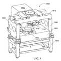
- FIG. 1depicts an embodiment of a system for imprint lithography
- FIG. 2depicts an imprint lithography system enclosure
- FIG. 3depicts an embodiment of an imprint lithography head coupled to an imprint lithography system
- FIG. 4depicts a projection view of an imprint head
- FIG. 5depicts an exploded view of an imprint head
- FIG. 6depicts a projection view of a first flexure member
- FIG. 7depicts a projection view of a second flexure member
- FIG. 8depicts a projection view of first and second flexure members coupled together
- FIG. 9depicts a projection view of a fine orientation system coupled to a pre-calibration system of an imprint head
- FIG. 10depicts a cross-sectional view of a pre-calibration system
- FIG. 11depicts a schematic diagram of a flexure system
- FIG. 12depicts a projection view of a motion stage and an imprint head of an imprint lithography system
- FIG. 13depicts a schematic diagram of a liquid dispense system
- FIG. 14depicts a projection view of an imprint head with a light source and camera optically coupled to the imprint head
- FIGS. 15 and 16depict side views of an interface between a liquid droplet and a portion of a template
- FIG. 17depicts a cross-sectional view a first embodiment of template configured for liquid confinement at the perimeter of the template
- FIG. 18depicts a cross-sectional view a second embodiment of template configured for liquid confinement at the perimeter of the template
- FIGS. 19A-Ddepict cross-sectional views of a sequence of steps of a template contacting a liquid disposed on a substrate.
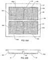
- FIGS. 20A-Bdepict top and cross-sectional views, respectively, of a template having a plurality of patterning areas and borders;
- FIG. 21depicts a projection view of a rigid template support system coupled to a pre-calibration system of an imprint head
- FIG. 22depicts an imprint head coupled to an X-Y motion system
- FIGS. 23A-23Fdepict cross-sectional views of a negative imprint lithography process
- FIGS. 24A-24Ddepict cross-sectional views of a negative imprint lithography process with a transfer layer
- FIGS. 25A-25Ddepict cross-sectional views of a positive imprint lithography process
- FIGS. 26A-26Cdepict cross-sectional views of a positive imprint lithography process with a transfer layer
- FIGS. 27A-27Ddepict cross-sectional views of a combined positive and negative imprint lithography process
- FIG. 28depicts a schematic of an optical alignment measuring device positioned over a template and substrate
- FIG. 29depicts a scheme for determining the alignment of a template with respect to a substrate using alignment marks by sequentially viewing and refocusing
- FIG. 30depicts a scheme for determining the alignment of a template with respect to a substrate using alignment marks and polarized filters
- FIG. 31depicts a top view of an alignment mark that is formed from polarizing lines
- FIGS. 32A-32Cdepict top views of patterns of curable liquid applied to a substrate
- FIGS. 33A-33Cdepict a scheme for removing a template from a substrate after curing
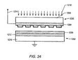
- FIG. 34depicts an embodiment of a template positioned over a substrate for electric field based lithography
- FIGS. 35A-35Ddepict a first embodiment of a process for forming nanoscale structures using contact with a template
- FIGS. 36A-36Cdepict a first embodiment of a process for forming nanoscale structures without contacting a template
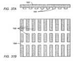
- FIGS. 37A-37Bdepict a template that includes a continuous patterned conductive layer disposed on a non-conductive base
- FIG. 38depicts a motion stage having a substrate tilt module
- FIG. 39depicts a motion stage that includes a fine orientation system.
- FIG. 40depicts a schematic drawing of a substrate support
- FIG. 41depicts a schematic drawing of an imprint lithography system that includes an imprint head disposed below a substrate support.
- Embodiments presented hereingenerally relate to systems, devices, and related processes of manufacturing small devices. More specifically, embodiments presented herein relate to systems, devices, and related processes of imprint lithography. For example, these embodiments may be used for imprinting sub 100 nm features on a substrate, such as a semiconductor wafer. It should be understood that these embodiments may also be used to manufacture other kinds of devices including, but not limited to: patterned magnetic media for data storage, micro-optical devices, micro-electro-mechanical system, biological testing devices, chemical testing and reaction devices, and X-ray optical devices.
- Imprint lithography processeshave demonstrated the ability to replicate high-resolution (sub-50 nm) images on substrates using templates that contain images as topography on their surfaces.
- Imprint lithographymay be used in patterning substrates in the manufacture of microelectronic devices, optical devices, MEMS, opto-electronics, patterned magnetic media for storage applications, etc.
- Imprint lithography techniquesmay be superior to optical lithography for making three-dimensional structures such as micro lenses and T-gate structures.
- Components of an imprint lithography systemincluding the template, substrate, liquid and any other materials that may affect the physical properties of the system, including but not limited to surface energy, interfacial energies, Hamacker constants, Van der Waals' forces, viscosity, density, opacity, etc., are engineered to properly accommodate a repeatable process.
- FIG. 1depicts an embodiment of a system for imprint lithography 3900 .
- System 3900includes an imprint head 3100 .
- Imprint head 3100is mounted to an imprint head support 3910 .
- Imprint head 3100is configured to hold a patterned template 3700 .
- Patterned template 3700includes a plurality of recesses that define a pattern of features to be imprinted into a substrate.
- Imprint head 3100 or motion stage 3600is further configured to move patterned template 3700 toward and away from a substrate to be imprinted during use.
- System 3900also includes a motion stage 3600 .
- Motion stage 3600is mounted to motion stage support 3920 .
- Motion stage 3600is configured to hold a substrate and move the substrate in a generally planar motion about motion stage support 3920 .
- System 3900further includes a curing light system 3500 coupled to imprint head 3100 .
- Activating light system 3500is configured to produce a curing light and direct the produced curing light through patterned template 3700 coupled to imprint head 3100 .
- Curing lightincludes light at an appropriate wavelength to cure a polymerizable liquid. Curing light includes ultraviolet light, visible light, infrared light, x-ray radiation and electron beam radiation.
- Imprint head support 3910is coupled to motion stage support 3920 by bridging supports 3930 . In this manner imprint head 3100 is positioned above motion stage 3600 .
- Imprint head support 3910 , motion stage support 3920 and bridging supports 3930are herein collectively referred to as the system “body.”
- the components of the system bodymay be formed from thermally stable materials. Thermally stable materials have a thermal expansion coefficient of less than about 10 ppm/deg. C. at about room temperature (e.g. 25 deg C.). In some embodiments, the material of construction may have a thermal expansion coefficient of less than about 10 ppm/deg. C., or less than 1 ppm/deg. C.
- Motion stage support 3920 and bridging supports 3930are coupled to a support table 3940 .
- Support table 3940provides a substantially vibration free support for the components of system 3900 .
- Support table 3940isolates system 3900 from ambient vibrations (e.g., due to works, other machinery, etc.).
- Motion stages and vibration isolation support tablesare commercially available from Newport Corporation of Irvine, Calif.
- the “X-axis”refers to the axis that runs between bridging supports 3930 .
- the “Y-axis”refers to the axis that is orthogonal to the X-axis.
- the “X-Y plane”is a plane defined by the X-axis and the Y-axis.
- the “Z-axis”refers to an axis running from motion stage support 3920 to imprint head support 3910 , orthogonal to the X-Y plane.
- an imprint processinvolves moving the substrate, or the imprint head, along an X-Y plane until the proper position of the substrate with respect to the patterned template is achieved. Movement of the template, or motion stage, along the Z-axis, will bring the patterned template to a position that allows contact between the patterned template and a liquid disposed on a surface of the substrate.
- System 3900may be placed in an enclosure 3960 , as depicted in FIG. 2 .
- Enclosure 3960encompasses imprint lithography system 3900 and provides a thermal and air barrier to the lithography components.
- Enclosure 3960includes a movable access panel 3962 that allows access to the imprint head and motion stage when moved to an “open” position, as depicted in FIG. 2 . When in a “closed” position, the components of system 3900 are at least partially isolated from the room atmosphere.
- Access panel 3962also serves as a thermal barrier to reduce the effects of temperature changes within the room on the temperature of the components within enclosure 3960 .
- Enclosure 3960includes a temperature control system. A temperature control system is used to control the temperature of components with enclosure 3960 .
- temperature control systemis configured to inhibit temperature variations of greater than about 1° C. within enclosure 3960 . In some embodiments, a temperature control system inhibits variations of greater than about 0.1° C. In one embodiment, thermostats or other temperature measuring devices in combination with one or more fans may be used to maintain a substantially constant temperature with enclosure 3960 .
- a computer controlled user interface 3964may be coupled to enclosure 3960 .
- User interface 3964may depict the operating parameters, diagnostic information, job progress and other information related to the functioning of the enclosed imprint system 3900 .
- User interface 3964may also be configured to receive operator commands to alter the operating parameters of system 3900 .
- a staging support 3966may also be coupled to enclosure 3960 .
- Staging support 3966is used by an operator to support substrates, templates and other equipment during an imprint lithography process.
- staging support 3966may include one or more indentations 3967 configured to hold a substrate (e.g., a circular indentation for a semiconductor wafer).
- Staging support 3966may also include one or more indentations 3968 for holding a template.
- Additional componentsmay be present depending on the processes that the imprint lithography system is designed to implement.
- semiconductor processing equipmentincluding, but not limited to, an automatic wafer loader, an automatic template loader and an interface to a cassette loader (all not shown) may be coupled to imprint lithography system 3900 .
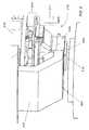
- FIG. 3depicts an embodiment of a portion of an imprint head 3100 .
- Imprint head 3100includes a pre-calibration system 3109 and a fine orientation system 3111 coupled to the pre-calibration system.
- Template support 3130is coupled to fine orientation system 3111 .
- Template support 3130is designed to support and couple a template 3700 to fine orientation system 3111 .
- a disk-shaped flexure ring 3124which makes up a portion of the pre-calibration system 3109 is coupled to imprint head housing 3120 .
- Imprint head housing 3120is coupled to a middle frame 3114 with guide shafts 3112 a , 3112 b .
- three (3) guide shaftsmay be used (the back guide shaft is not visible in FIG. 4 ) to provide a support for housing 3120 .
- Sliders 3116 a and 3116 b coupled to corresponding guide shafts 3112 a , 3112 b about middle frame 3114are used to facilitate the up and down motion of housing 3120 .
- a disk-shaped base plate 3122is coupled to the bottom portion of housing 3120 .
- Base plate 3122may be coupled to flexure ring 3124 .
- Flexure ring 3124supports the fine orientation system components that include first flexure member 3126 and second flexure member 3128 . The operation and configuration of the flexure members 3126 , 3128 are discussed in detail below.
- FIG. 5depicts an exploded view of imprint head 3700 .
- actuators 3134 a , 3134 b , 3134 care fixed within housing 3120 and coupled to base plate 3122 and flexure ring 3124 .
- motion of actuators 3134 a , 3134 b , and 3134 ccontrols the movement of flexure ring 3124 .
- Motion of actuators 3134 a , 3134 b , and 3134 cmay allow for a coarse pre-calibration.
- actuators 3134 a , 3134 b , and 3134 cmay be equally spaced around housing 3120 .
- Actuators 3134 a , 3134 b , 3134 c and flexure ring 3124together form the pre-calibration system. Actuators 3134 a , 3134 b , 3134 c allow translation of flexure ring 3124 along the Z-axis to control the gap accurately.
- Imprint head 3100also include a mechanism that enables fine orientation control of template 3700 so that proper orientation alignment may be achieved and a uniform gap may be maintained by the template with respect to a substrate surface. Alignment and gap control is achieved, in one embodiment, by the use of first and second flexure members, 3126 and 3128 , respectively.
- first flexure member 3126includes a plurality of flexure joints 3160 coupled to corresponding rigid bodies 3164 and 3166 .
- Flexure joints 3160may be notch shaped to provide motion of rigid bodies 3164 and 3166 about pivot axes that are located along the thinnest cross section of the flexure joints.
- Flexure joints 3160 and rigid body 3164together form arm 3172
- additional flexure joints 3160 and rigid body 3166together form arm 3174 .
- Arms 3172 and 3174are coupled to and extend from first flexure frame 3170 .
- First flexure frame 3170has an opening 3182 , which allows curing light (e.g., ultraviolet light) to pass through first flexure member 3126 .
- curing lighte.g., ultraviolet light
- four flexure joints 3160allow motion of first flexure frame 3170 about a first orientation axis 3180 . It should be understood, however, that more or less flexure joints may be used to achieve the desired control.
- First flexure member 3126is coupled to second flexure member 3128 through fist flexure frame 3170 , as depicted in FIG. 8 .
- First flexure member 3126also includes two coupling members 3184 and 3186 .
- Coupling members 3184 and 3186include openings that allow attachment of the coupling members to flexure ring 3124 using any suitable fastening means. Coupling members 3184 and 3186 are coupled to first flexure frame 3170 via arms 3172 and 3174 as depicted.
- Second flexure member 3128includes a pair of arms 3202 and 3204 extending from second flexure frame 3206 , as depicted in FIG. 7 .
- Flexure joints 3162 and rigid body 3208together form arm 3202
- additional flexure joints 3162 and rigid body 3210together form arm 3204 .
- Flexure joints 3162may be notch shaped to provide motion of rigid bodies 3210 and 3204 about pivot axes that are located along the thinnest cross section of the flexure joints.
- Arms 3202 and 3204are coupled to and extend from template support 3130 .
- Template support 3130is configured to hold and retain at least a portion of a patterned template.
- Template support 3130also has an opening 3212 , which allows curing light (e.g., ultraviolet light) to pass through second flexure member 3128 .
- curing lighte.g., ultraviolet light
- four flexure joints 3162allow motion of template support 3130 about a second orientation axis 3200 . It should be understood, however, that more or less flexure joints may be used to achieve the desired control.
- Second flexure member 3128also includes braces 3220 and 3222 . Braces 3220 and 3222 include openings that allow attachment of the braces to portions of first flexure member 3126 .
- first flexure member 3126 and second flexure member 3128are joined as shown in FIG. 8 to form fine orientation section 3111 .
- Braces 3220 and 3222are coupled to first flexure frame 3170 such that the first orientation axis 3180 of first flexure member 3126 and second orientation axis 3200 of second flexure member are substantially orthogonal to each other.
- first orientation axis 3180 and second orientation axis 3200intersect at a pivot point 3252 at approximately the center region of a patterned template 3700 disposed in template support 3130 . This coupling of the first and second flexure member allows fine alignment and gap control of patterned template 3700 during use.
- first and second flexure membersare depicted as discrete elements, it should be understood that the first and second flexure member may be formed from a single machined part where the flexure members are integrated together.
- Flexure members 3126 and 3128are coupled by mating of surfaces such that motion of patterned template 3700 occurs about pivot point 3252 , substantially reducing “swinging” and other motions that may shear imprinted features following imprint lithography.
- Fine orientation sectionimparts negligible lateral motion at the template surface and negligible twisting motion about the normal to the template surface due to selectively constrained high structural stiffness of the flexure joints.
- Another advantage of using the herein described flexure membersis that they do not generate substantial amounts of particles, especially when compared with frictional joints. This is offers an advantage for imprint lithography processes, as particles may be disrupt such processes.
- FIG. 9depicts the assembled fine orientation system coupled to the pre-calibration system.
- Patterned template 3700is positioned within template support 3130 that is part of second flexure member 3128 .
- Second flexure member 3128is coupled to first flexure member 3126 in a substantially orthogonal orientation.
- First flexure member 3124is coupled to flexure ring 3124 via coupling members 3186 and 3184 .
- Flexure ring 3124is coupled to base plate 3122 , as has been described above.
- FIG. 10represents a cross-section of the pre-calibration system looking through cross-section 3260 .
- flexure ring 3124is coupled to base plate 3122 with actuator 3134 .
- Actuator 3134includes an end 3270 coupled to a force detector 3135 that contacts flexure ring 3124 .
- force detector 3135that contacts flexure ring 3124 .
- actuator 3134causes movement of end 3270 toward or away from flexure ring 3124 .
- the movement of end 3270 toward flexure ring 3124induces a deformation of the flexure ring and causes translation of the fine orientation system along the Z-axis toward the substrate.
- Movement of base 3270 away from flexure ringallows the flexure ring to move to its original shape and, in the process, moves the fine orientation stage away from the substrate.
- the templateis disposed in a template holder coupled to the fine orientation system, as depicted in previous figures.
- the templateis brought into contact with a liquid on a surface of a substrate. Compression of the liquid on the substrate as the template is brought closer to the substrate causes a resistive force to be applied by the liquid onto the template.
- This resistive forceis translated through the fine orientation system and to flexure ring 3124 as shown in both FIGS. 9 and 10 .
- the force applied against flexure ring 3124will also be translated as a resistive force to actuators 3134 .
- the resistive force applied to an actuator 3134may be determined using force sensor 3135 . Force sensor 3135 may be coupled to actuator 3134 such that a resistive force applied to actuator 3135 during use may be determined and controlled.
- FIG. 11depicts a flexure model, denoted generally as 3300 , useful in understanding the principles of operation of a fine decoupled orientation stage, such as the fine orientation section described herein.
- Flexure model 3300may include four parallel joints: Joints 1 , 2 , 3 and 4 , that provide a four-bar-linkage system in its nominal and rotated configurations.
- Line 3310denotes an axis of alignment of Joints 1 and 2 .
- Line 3312denotes an axis of alignment of Joints 3 and 4 .
- Angle ⁇ 1represents an angle between a perpendicular axis through the center of template 3700 and line 3310 .
- Angle ⁇ 2represents a perpendicular axis through the center of template 3700 and line 3310 .
- Angles ⁇ 1 and ⁇ 2are selected so that the compliant alignment axis (or orientation axis) lies substantially at the surface of template 3700 .
- rigid body 3314 between Joints 2 and 3may rotate about an axis depicted by Point C.
- Rigid body 3314may be representative of template support 3130 of second flexure member 3128 .
- Fine orientation systemgenerates pure tilting motions with no substantial lateral motions at the surface of a template coupled to the fine orientation system.
- the use of flexure armsmay provide fine orientation system with high stiffness in the directions where side motions or rotations are undesirable and lower stiffness in directions where necessary orientation motions are desirable.
- Fine orientation systemtherefore allows rotations of the template support, and therefore the template, about the pivot point at the surface of template, while providing sufficient resistance in a direction perpendicular to the template and parallel to the template to maintain the proper position with respect to the substrate. In this manner a passive orientation system is used for orientation of the template to a parallel orientation with respect to a template.
- Passiverefers to a motion that occurs without any user or programmable controller intervention, i.e., the system self-corrects to a proper orientation by contact of the template with the liquid.
- Alternate embodiments in which the motion of the flexure arms is controlled by motors to produce an active flexuremay also be implemented.
- Motion of the fine orientation stagemay be activated by direct or indirect contact with the liquid.
- the fine orientation stageis passive, then it is, in one embodiment, designed to have the most dominant compliance about two orientation axes.
- the two orientation axeslie orthogonal to each other and lie on the imprinting surface of an imprinting member disposed on the fine orientation stage.
- the two orthogonal torsional compliance valuesare set to be the same for a symmetrical imprinting member.
- a passive fine orientation stageis designed to alter the orientation of the template when the template is not parallel with respect to a substrate. When the template makes contact with liquid on the substrate, the flexure members compensate for the resulting uneven liquid pressure on the template. Such compensation may be affected with minimal or no overshoot.
- a fine orientation stage as described abovemay hold the substantially parallel orientation between the template and substrate for a sufficiently long period to allow curing of the liquid.
- Imprint head 3100is mounted to imprint head support 3910 as depicted in FIG. 1 .
- imprint head 3910is mounted such that the imprint head remains in a fixed position at all times. During use, all movement along the X-Y plane is performed to the substrate by motion stage 3600 .
- Motion stage 3600is used to support a substrate to be imprinted and move the substrate along an X-Y plane during use.
- Motion stagein some embodiments, is capable of moving a substrate over distances of up to several hundred millimeters with an accuracy of at least ⁇ 30 nm, preferably with an accuracy of about ⁇ 10 nm.
- motion stageincludes a substrate chuck 3610 that is coupled to carriage 3620 , as depicted in FIG. 12 .
- Carriage 3620is moved about a base 3630 on a frictional bearing system or a non-frictional bearing system. In one embodiment, a non-frictional bearing system that includes an air bearing is used.
- Carriage 3620is suspended above base 3630 of motion stage using, in one embodiment, an air layer (i.e., the “air bearing”).
- an air layeri.e., the “air bearing”.
- Magnetic or vacuum systemsmay be used to provide a counter balancing force to the air bearing level. Both magnetic based and vacuum based systems are commercially available from a variety of suppliers and any such systems may be used in an imprint lithography process.
- One example of a motion stage that is applicable to imprint lithography processesis the Dynam YX motion stage commercially available from Newport Corporation, Irvine Calif.
- the motion stagealso may include a tip tilt stage similar to the calibration stage, designed to approximately level the substrate to the X Y motion plane. It also may include one or more theta stages to orient the patterns on the substrate to the X Y motion axes.
- System 3900also includes a liquid dispense system which is used to dispense a curable liquid onto a substrate.
- Liquid dispense systemis coupled to the system body.
- a liquid dispense systemis coupled to imprint head 3100 .
- FIG. 3depicts liquid dispenser head 2507 of a liquid dispense system extending out from cover 3127 of imprint head 3100 .
- Various components of liquid dispense system 3125may be disposed in cover 3127 of imprint head 3100 .
- a liquid dispense systemincludes a liquid container 2501 .
- Liquid container 2501is configured to hold an activating light curable liquid.
- Liquid container 2501is coupled to a pump 2504 via inlet conduit 2502 .
- An inlet valve 2503is positioned between liquid container 2501 and pump 2504 to control flow of through inlet conduit 2502 .
- Pump 2504is coupled to a liquid dispenser head 2507 via outlet conduit 2506 .
- Liquid dispense systemis configured to allow precise volume control of the amount of liquid dispensed onto an underlying substrate.
- liquid controlis achieved using a piezoelectric valve as pump 2504 .
- Piezoelectric valvesare available commercially available from the Lee Company, Westbrook, Conn.
- a curable liquidis drawn into pump 2504 through inlet conduit 2502 .
- pump 2504is activated to force a predetermined volume of liquid through outlet conduit 2506 .
- the liquidis then dispensed through liquid dispenser head 2507 onto the substrate.
- liquid volume controlis achieved by control of pump 2504 . Rapid switching of the pump from an open to closed state allows a controlled amount of liquid to be sent to dispenser head 2507 .
- Pump 2504is configured to dispense liquid in volumes of less than about 1 ⁇ L.
- the operation of pump 2504may allow either droplets of liquid or a continuous pattern of liquid to be dispensed onto the substrate. Droplets of liquid are applied by rapidly cycling the pump from an open to closed state. A stream of liquid is produced on the substrate by leaving the pump in an open state and moving the substrate under the liquid dispenser head.
- liquid volume controlmay be achieved by use of liquid dispenser head 2507 .
- pump 2504is used to supply a curable liquid to liquid dispenser head 2507 .
- Small drops of liquid whose volume may be accurately specifiedare dispensed using a liquid dispensing actuator.
- liquid dispensing actuatorsinclude micro-solenoid valves or piezo-actuated dispensers. Piezo-actuated dispensers are commercially available from MicroFab Technologies, Inc., Plano, Tex.
- Liquid dispensing actuatorsare incorporated into liquid dispenser head to allow control of liquid dispensing. Liquid dispensing actuators are configured to dispense between about 50 pL to about 1000 pL of liquid per drop of liquid dispensed.
- Linear encodersinclude a scale coupled to the moving object and a reader coupled to the body.
- the scalemay be formed from a variety of materials including glass, glass ceramics, and steel.
- the scaleincludes a number of markings that are read by the reader to determine a relative or absolute position of the moving object.
- the scaleis coupled to the motion stage by means that are known in the art.
- a readeris coupled to the body and optically coupled to the scale.
- an exposed linear encodermay be used.
- Encodersmay be configured to determine the position of the motion stage along either a single axis, or in a two-axis plane.
- An example of an exposed two-axis linear encoderis the PP model encoder available from Heidenhain Corporation, Schaumburg, Ill.
- encodersare built into many commercially available X-Y motion stages. For example, the Dynam YX motion stage available from Newport Corp has a two-axis encoder built into the system.
- the coarse position of the template along the Z-axisis also determined using a linear encoder.
- an exposed linear encodermay be used to measure the position of the template.
- a scale of the linear encoderin one embodiment, is coupled to the pre-calibration ring of the imprint head. Alternatively, the scale may be coupled directly to the template support 3130 .
- the readeris coupled to the body and optically coupled to the scale. Position of the template is determined along the Z-axis by use of encoders.
- an air gauge 3135may be coupled to imprint head 3100 , as depicted in FIG. 3 .
- Air gauge 3135is used to determine whether a substrate disposed on a motion stage is substantially parallel to a reference plane.
- an “air gauge”refers to a device that measures the pressure of a stream of air directed toward a surface. When a substrate is disposed under an outlet of air gauge 3135 , the distance the substrate is from the outlet of air gauge 3135 will influence the pressure the air gauge senses. Generally, the further away from the air gauge the substrate is, the lesser the pressure.
- air gauge 3135may be used to determine differences in pressure resulting from changes in the distance between the substrate surface and the air gauge. By moving air gauge 3135 along the surface of the substrate, the air gauge determines the distance between the air gauge and the substrate surface at the various points measured. The degree of planarity of the substrate with respect to the air gauge is determined by comparing the distance between the air gauge and substrate at the various points measured. The distance between at least three points on the substrate and the air gauge is used to determine if a substrate is planar. If the distance is substantially the same, the substrate is considered to be planar. Significant differences in the distances measured between the substrate and the air gauge indicates a non-planar relationship between the substrate and the air gauge.
- This non-planar relationshipmay be caused by the non-planarity of the substrate or a tilt of the substrate.
- a tilt of the substratePrior to use, a tilt of the substrate is corrected to establish a planar relationship between the substrate and the template template using the tip tilt stage attached to the X Y stage.
- Suitable air gaugesmay be obtained from Senex Inc.
- the substrate or templateis placed within the measuring range of the air gauge.
- Motion of the substrate toward the air gaugemay be accomplished by either Z-axis motion of the imprint head or Z-axis motion of the motion stage.
- a light curable liquidis disposed on a surface of the substrate.
- a patterned templateis brought into contact with the light curable liquid and activating light is applied to the light curable liquid.
- activating lightmeans light that may affect a chemical change. Activating light may include ultraviolet light (e.g., light having a wavelength between about 200 nm to about 400 nm), actinic light, visible light or infrared light. Generally, any wavelength of light capable of affecting a chemical change may be classified as activating. Chemical changes may be manifested in a number of forms. A chemical change may include, but is not limited to, any chemical reaction that causes a polymerization or a cross-linking reaction to take place.
- the activating lightin one embodiment, is passed through the template prior to reaching the composition. In this manner the light curable liquid is cured to form structures complementary to the structures formed on the template.
- activating light source 3500is an ultraviolet light source capable of producing light having a wavelength between about 200 nm to about 400 nm.
- Activating light source 3500is optically coupled to the template as depicted in FIG. 1 .
- activating light source 3500is positioned proximate to imprint head 3100 .
- Imprint head 3100includes a mirror 3121 (depicted in FIG. 4 , which reflects light from the activating light source to the patterned template. Light passes through an opening in the body of imprint head 3100 and is reflected by mirror 3121 toward 3700 . In this manner, activating light source irradiates a patterned template without being disposed in imprint head 3100 .
- activating light sourcesproduce a significant amount of heat during use. If activating light source 3500 is too close to imprint system 3500 , heat from the light source will radiate toward the body of the imprint system and may cause the temperature of portions of the body to increase. Since many metals expand when heated, the increase in temperature of a portion of the body of the imprint system may cause an expansion of the body to expand. This expansion may affect the accuracy of the imprint system when sub-100 nm features are being produced.
- activating light sourceis positioned at a sufficient distance from the body such that system body is insulated from heat produced by activating light source 3500 by the intervening air between activating light source 3500 and imprint head 3100 .
- FIG. 14depicts an activating light source 3500 optically coupled to imprint head 3100 .
- Activating light source 3500includes an optical system 3510 that projects light generated by a light source toward imprint head 3100 . Light passes from optical system 3510 into imprint head 3100 via opening 3123 . Light is then reflected toward a template coupled to imprint head 3110 by mirror 3121 disposed within the imprint head (see FIG. 4 ). In this manner, the light source is thermally insulated from the body.
- a suitable light sourcemay be obtained from OAI Inc, Santa Clara Calif.
- One or more optical measuring devicesmay be coupled to imprint head 3910 and/or motion stage 3920 .
- an optical measuring deviceis any device that allows the position and/or orientation of a template with respect to a substrate to be determined.
- a through the template optical imaging system 3800is optically coupled to the imprint head.
- Optical imaging system 3800includes an optical imaging device 3810 and an optical system 3820 .
- Optical imaging device 3810in one embodiment, is a CCD microscope.
- Optical imaging system 3800is optically coupled to the template through imprint head.
- Optical imaging system 3800is also optically coupled to a substrate, when the substrate is disposed under the patterned template.
- Optical imaging system 3800is used to determine the placement error between a patterned template and an underlying substrate as described herein.
- mirror 3121(depicted in FIG. 4 ) is movable within the imprint head. During an alignment or optical inspection process, mirror 3121 is moved out of the optical path of the optical imaging system.
- the substrate or templateis placed within the measuring range (e.g., the filed of view) of the air optical imaging system.
- Motion of the substrate toward the optical imagining systemmay be accomplished by either Z-axis motion of the imprint head or Z-axis motion of the motion stage.
- a light curable liquidis placed on a substrate and a template is brought into contact with the liquid during an imprint lithography process.
- the curable liquidis a low viscosity liquid monomer solution.
- a suitable solutionmay have a viscosity ranging from about 0.01 cps to about 100 cps (measured at 25° C.).
- Low viscositiesare especially desirable for high-resolution (e.g., sub-100 nm) structures. Low viscosities also lead to faster gap closing. Additionally, low viscosities result in faster liquid filling of the gap area at low pressures.
- the viscosity of the solutionshould be at or below about 30 cps, or more preferably below about 5 cps (measured at 25° C.).
- the curable liquidmay be composed of a variety of polymerizable materials. Generally, any photopolymerizable material may be used. Photopolymerizable materials may include a mixture of monomers and a photoinitiator. In some embodiments, the curable liquid may include one or more commercially available negative photoresist materials. The viscosity of the photoresist material may be reduced by diluting the liquid photoresist with a suitable solvent.
- a suitable curable liquidincludes a monomer, a silylated monomer, and an initiator.
- a crosslinking agent and a dimethyl siloxane derivativemay also be included.
- Monomersinclude, but are not limited to, acrylate and methacylate monomers. Examples of monomers include, but are not limited to, butyl acrylate, methyl acrylate, methyl methacrylate, or mixtures thereof.
- the monomermakes up approximately 25 to 50% by weight of the curable liquid. It is believed that the monomer ensures adequate solubility of the photoinitiator in the curable liquid. It is further believed that the monomer provides adhesion to an underlying organic transfer layer, when used.
- the curable liquidmay also include a silylated monomer.
- Silylated monomersin general are polymerizable compounds that include a silicon group. Classes of silylated monomers include, but are not limited to, silane acrylyl and silane methacrylyl derivatives. Specific examples include methacryloxypropyl tris(tri-methylsiloxy)silane and (3-acryloxypropyl)tris(tri-methoxysiloxy)-silane. Silylated monomers may be present in amounts from 25 to 50% by weight.
- the curable liquidmay also include a dimethyl siloxane derivative.
- dimethyl siloxane derivativesinclude, but are not limited to, (acryloxypropyl) methylsiloxane dimethylsiloxane copolymer, acryloxypropyl methylsiloxane homopolymer, and acryloxy terminated polydimethylsiloxane.
- Dimethyl siloxane derivativesare present in amounts from about 0 to 50% by weight. It is believed that the silylated monomers and the dimethyl siloxane derivatives may impart a high oxygen etch resistance to the cured liquid. Additionally, both the silylated monomers and the dimethyl siloxane derivatives are believed to reduce the surface energy of the cured liquid, therefore increasing the ability of the template to release from the surface.
- the silylated monomers and dimethyl siloxane derivatives listed hereinare all commercially available from Gelest, Inc.
- any material that may initiate a free radical reactionmay be used as the initiator.
- the initiatoris a photoinitiator.
- examples of initiatorsinclude, but are not limited to, alpha-hydroxyketones (e.g., 1-hydroxycyclohexyl phenyl ketone, sold by Ciba-Geigy Specialty Chemical Division as Irgacure 184), and acylphosphine oxide initiators (e.g., phenylbis(2,4,6-trimethyl benzoyl) phosphine oxide, sold by Ciba-Geigy Specialty Chemical Division as Irgacure 819).
- alpha-hydroxyketonese.g., 1-hydroxycyclohexyl phenyl ketone, sold by Ciba-Geigy Specialty Chemical Division as Irgacure 184
- acylphosphine oxide initiatorse.g., phenylbis(2,4,6-trimethyl
- the curable liquidmay also include a crosslinking agent.
- Crosslinking agentsare monomers that include two or more polymerizable groups.
- polyfunctional siloxane derivativesmay be used as a crosslinking agent.
- An example of a polyfunctional siloxane derivativeis 1,3-bis(3-methacryloxypropyl)-tetramethyl disiloxane.
- a curable liquidmay include a mixture of 50% by weight of n-butyl acrylate and 50% (3-acryloxypropyl) tris-trimethylsiloxane-silane. To this mixture 3% by weight mixture of a 1:1 Irgacure 819 and Irgacure 184 and 5% of the crosslinker 1,3-bis(3-methacryloxypropyl)-tetramethyl disiloxane may be added. The viscosity of this mixture is less than 30 cps measured at about 25° C.
- the curable liquidmay be formed of a monomer, an acid-generating photo-agent, and a base-generating photo-agent.
- the monomerinclude, but are not limited to, phenolic polymers and epoxy resins.
- the acid-generating photo-agentis a compound that releases acid when treated with activating light. The generated acid catalyzes polymerization of the monomer.
- the acid-generating additiveis selected to be sensitive to radiation at the first wavelength ⁇ 1 , which, in some implementations, is in the visible or near ultraviolet (near UV) range.
- the first wavelength ⁇ 1is selected to be approximately 400 nm or longer.
- a base generating photo-agentis also added to the monomer.
- the base-generating photo-agentmay inhibit curing of the monomer near the interface of the template.
- the base generating photo-agentmay be sensitive to radiation at a second wavelength ⁇ 2 , yet inert or substantially inert to radiation at the first wavelength ⁇ 1 .
- the second wavelength ⁇ 2should be selected so that radiation at the second wavelength is primarily absorbed near the surface of the monomer at the interface with the template and does not penetrate very far into the curable liquid.
- a base generating additivethat is sensitive to radiation having a wavelength ⁇ 2 in the deep UV range, in other words, radiation having a wavelength in the range of about 190-280 nm, may be used.
- a curable liquidthat includes a monomer, an acid-generating photo-agent and a base-generating photo-agent is deposited onto a substrate.
- a templateis brought into contact with the curable liquid.
- the curable liquidis then exposed to radiation at a first wavelength ⁇ 1 and a second wavelength ⁇ 2 of light at substantially the same time.
- the curing liquidmay be exposed to the radiation at the second wavelength ⁇ 2 and subsequently to the radiation at the first wavelength ⁇ 1 . Exposure of the curable liquid to radiation at the second wavelength ⁇ 2 produces an excess of base near the interface with the template.
- the excess baseserves to neutralize the acid that is produced by exposure of the curable liquid to radiation at the first wavelength ⁇ 1 , thereby inhibiting the acid from curing the curable liquid. Since the radiation at the second wavelength ⁇ 2 has a shallow penetration depth into the curable liquid, the base produced by that radiation only inhibits curing of the curable liquid at or near the interface with the template. The remainder of the curable liquid is cured by exposure to the longer wavelength radiation ( ⁇ 1 ) which penetrates throughout the curable liquid.
- U.S. Pat. No. 6,218,316 entitled “Planarization of Non-Planar Surfaces in Device Fabrication”describes additional details concerning this process and is incorporated herein by reference.
- the curable liquidmay include a photosensitive agent which, when exposed, for example, to deep UV radiation, decomposes to produce one or more gases such as hydrogen (H 2 ), nitrogen (N 2 ), nitrous oxide (N 2 O), sulfur tri-oxide (SO 3 ), acetylene (C 2 H 2 ), carbon dioxide (CO 2 ), ammonia (NH 3 ) or methane (CH 4 ).
- a photosensitive agentwhich, when exposed, for example, to deep UV radiation, decomposes to produce one or more gases such as hydrogen (H 2 ), nitrogen (N 2 ), nitrous oxide (N 2 O), sulfur tri-oxide (SO 3 ), acetylene (C 2 H 2 ), carbon dioxide (CO 2 ), ammonia (NH 3 ) or methane (CH 4 ).
- Radiation at a first wavelength ⁇ 1such as visible or near UV, may be used to cure the curable liquid, and the deep UV radiation ( ⁇ 2 ) may be used to produce one or more of the for
- a curable liquidmay be composed of a monomer that cures to form a polymer that may be decomposed by exposure to light.
- a polymer with a doubly substituted carbon backboneis deposited on the substrate.
- the curable liquidis exposed to radiation at a first wavelength ⁇ 1 (e.g., greater than 400 nm) and radiation at the second wavelength ⁇ 2 in the deep UV range. Radiation at the first wavelength serves to cure the curable liquid.
- ⁇ 1e.g., greater than 400 nm
- Radiation at the first wavelengthserves to cure the curable liquid.
- the curable liquidis exposed to the second wavelength ⁇ 2 , scission occurs at the substituted carbon atoms. Since deep UV radiation does not penetrate deeply into the curable liquid, the polymer decomposes only near the interface with the template.
- the decomposed surface of the cured liquidfacilitates separation from the template.
- Other functional groups which facilitate the photo-decomposition of the polymeralso can be used.
- U.S. Pat. No. 6,218,316describes additional details concerning this process and is incorporated herein by reference.
- an imprint lithography templateis manufactured using processes including, but not limited to: optical lithography, electron beam lithography, ion-beam lithography, x-ray lithography, extreme ultraviolet lithography, scanning probe lithography, focused ion beam milling, interferometric lithography, epitaxial growth, thin film deposition, chemical etch, plasma etch, ion milling, reactive ion etch or a combination of the above.
- Methods for making patterned templatesare described in U.S. patent application Ser. No. 10/136,188 filed May 1, 2002 entitled “Methods of Manufacturing a Lithography Template” to Voison which is incorporated herein by reference.
- the imprint lithography templateis substantially transparent to activating light.
- the templateincludes a body having a lower surface.
- the templatefurther includes a plurality of recesses on the lower surface extending toward the top surface of the body.
- the recessesmay be of any suitable size, although typically at least a portion of the recesses has a feature size of less than about 250 nm.
- a templateis formed from quartz.
- Other materialsmay be used to form the template and include, but are not limited to: silicon germanium carbon, gallium nitride, silicon germanium, sapphire, gallium arsinide, epitaxial silicon, poly-silicon, gate oxide, silicon dioxide or combinations thereof.
- Templatesmay also include materials used to form detectable features, such as alignment markings.
- detectable featuresmay be formed of SiO x , where X is less than 2. In some embodiments, X is about 1.5. In another example, detectable features may be formed of a molybdenum silicide.
- Both SiOx and molybdenum silicideare optically transparent to light used to cure the polymerizable liquid. Both materials, however, are substantially opaque to visible light. Use of these materials allows alignment marks to be created on the template that will not interfere with curing of the underlying substrate.
- the templateis treated with a surface treatment material to form a thin layer on the surface of the template.
- a surface treatment processis optimized to yield a low surface energy coating.
- Such a coatingis used in preparing imprint templates for imprint lithography.
- Treated templateshave desirable release characteristics relative to untreated templates.
- Untreated template surfacespossess surface free energies of about 65 dynes/cm or more.
- a treatment procedure disclosed hereinyields a surface treatment layer that exhibits a high level of durability. Durability of the surface treatment layer allows a template to be used for numerous imprints without having to replace the surface treatment layer.
- the surface treatment layerin some embodiments, reduces the surface free energy of the lower surface measured at 25° C. to less than about 40 dynes/cm, or in some cases, to less than about 20 dynes/cm.
- a surface treatment layerin one embodiment, is formed by the reaction product of an alkylsilane, a fluoroalkylsilane, or a fluoroalkyltrichlorosilane with water. This reaction forms a silinated coating layer on the surface of the patterned template.
- a silinated surface treatment layeris formed from a reaction product of tridecafluoro-1,1,2,2-tetrahydrooctyl trichlorosilane with water.
- a surface treatment layermay be formed using either a liquid-phase process or a vapor-phase process. In a liquid-phase process, the substrate is immersed in a solution of precursor and solvent.
- a precursoris delivered via an inert carrier gas. It may be difficult to obtain a purely anhydrous solvent for use in a liquid-phase treatment. Water in the bulk phase during treatment may result in clump deposition, which will adversely affect the final quality or coverage of the coating.
- the templateis placed in a vacuum chamber, after which the chamber is cycle-purged to remove excess water. Some adsorbed water, however, remains on the surface of the template. A small amount of water, however, is believed to be needed to initiate a surface reaction, which forms the coating.
- the reactionmay be described by the formula: R—SiCl 3 +3H 2 O ⁇ R—Si(OH) 3 +3HCl
- the templateis brought to a desired reaction temperature via a temperature-controlled chuck.
- the precursoris then fed into the reaction chamber for a prescribed time.
- Reaction parameterssuch as template temperature, precursor concentration, flow geometries, etc. are tailored to the specific precursor and template substrate combination.
- the thickness of the surface treatment layeris controlled.
- the thickness of the surface treatment layeris kept at a minimal value to minimize the interference of the surface treatment layer with the feature size.
- a monolayer of the surface treatment layeris formed.
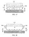
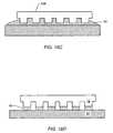
- FIGS. 20A and 20Bdepict top and cross-sectional views, respectively, of a patterned template with recesses having two depths.
- a templateincludes one or more patterning areas 401 .
- a first relatively shallow depthis associated with the recesses in the patterning areas of the template, as depicted in FIG. 20 B.
- the patterning areaincludes the area replicated during patterning of the template.
- the patterning areasare positioned within a region defined by the edges 407 of the template.
- Outer region 409is defined as the region that extends from an outer edge of any of the patterning areas to the edge of the template.
- the outer regionhas a depth that is substantially greater than the depth of the recesses in the patterning areas.
- the perimeter of the templateis herein defined as the patterning areas that are confined by outer region 409 . As depicted in FIG. 20A four patterning areas are positioned within the area defined by the template. The patterning areas are separated from the edges 407 of the template by outer region 409 .
- the “perimeter” of the templateis defined by edges 403 a , 403 b , 403 c , 403 d , 403 e , 403 f , 403 g , and 403 h of the patterning areas.
- the patterning areasmay be separated from each other by border regions 405 .
- Borders regionsare recesses that are positioned between the patterning areas that have a greater depth than the recesses of the pattering areas. As described below, both border regions and outer region inhibits the flow of liquid between the patterning regions or beyond the perimeter of the patterning areas, respectively.
- a template 12is formed such that the depth of one or more structures is relatively large compared to the depth of structures used to form the patterning region, as depicted in FIG. 15 .
- template 12is placed in a desired spaced relationship to substrate 20 .
- the gap (h 1 ) between the lower surface 536 of template 12 and substrate 20is much smaller than the gap (h 2 ) between recessed surface 534 and substrate 20 .
- h 1may be less than about 200 nm, while h 2 may be greater than about 10,000 nm.
- liquid 40leaves the region under recessed surface 534 and fills the gap between lower surface 536 and substrate 20 (as depicted in FIG. 16 ). It is believed that combinations of surface energies and capillary forces draw the liquid from the larger recess into the narrower region. As h 1 is decreased, forces applied to the liquid by template 12 may overcome capillary forces drawing the liquid under lower surface 536 . These forces may cause spreading of the liquid into the area under recessed surface 534 .
- the minimum value of h 1 at which the liquid is inhibited from spreading into a recess 532is referred to herein as the “minimum film thickness.” Additionally, as h 1 increases, the capillary forces are reduced, eventually allowing the liquid to spread into the deeper recessed regions. The maximum value of h 1 at which the capillary forces are sufficient to inhibit flow of liquid into the deeper recessed region is herein known as the “maximum film thickness.”
- template 12is formed such that a curable liquid placed on substrate 20 is inhibited from flowing beyond perimeter 412 of template 12 .
- height h 1is measured from substrate 20 to shallow recessed surface 552 .
- Shallow recessed surface 552extends to the perimeter of template 12 .
- the edge of the templateforms the height h 2 and is effectively infinite in comparison to height h 1 .
- a deep recessis formed at the outer edge of template 12 .
- Height h 2is measured between substrate 20 and deep recessed surface 554 .
- Height h 1is again measured between substrate 20 and shallow recessed surface 552 .
- height h 2is much larger than height h 1 . If h 1 is small enough, the activating light curable liquid remains in the gap between template 12 and substrate 20 while a curing agent is applied. Deeply recessed portions are particularly useful for liquid confinement in step and repeat processes as described herein.
- template 12 and substrate 20each have one or more alignment marks.
- Alignment marksmay be used to align template 12 and substrate 20 .
- one or more optical imaging devicese.g., microscopes, cameras, imaging arrays, etc. are used to determine alignment of the alignment marks.
- an alignment mark on the templatemay be substantially transparent to activating light.
- the alignment markmay be substantially opaque to alignment mark detection light.
- alignment mark detection light and light used for other measurement and analysis purposesis referred to as “analyzing light.”
- analyzing lightincludes, but is not limited to: visible light and/or infrared light.
- the alignment markmay be formed of a material different than the material of the body.
- the alignment markmay be formed from SiO x where x is about 1.5.
- the alignment markmay be formed of molybdenum silicide.
- the alignment markmay include a plurality of lines etched on a surface of the body. The lines are configured to substantially diffuse activating light, but produce an analyzable mark under analyzing light.
- one or more deep recesses as described abovemay project entirely through the body of the template to form openings in the template.
- An advantage of such openingsis that they may effectively ensure that height h 2 is very large with respect to h 1 at each opening.
- pressurized gas or vacuummay be applied to the openings. Pressurized gas or vacuum may also be applied to one or more openings after curing the liquid. For example, pressurized gas may be applied after curing as part of a peel and pull process to assist in separating the template from the cured liquid.
- an imprint headincludes a fine orientation system that allows for a “passive” orientation of the template with respect to the substrate.
- fine orientation systemmay include actuators coupled to the flexure arms. The actuators may allow “active” control of the fine orientation system.
- an operator or a programmable controllermonitors the orientation of the template with respect to the substrate. The operators or a programmable controller then alters the orientation of the template with respect to the substrate by operating the actuators. Movement of the actuators causes motion of the flexure arms to alter the orientation of the template. In this manner an “active” control of fine positioning of the template with respect to the substrate may be achieved.
- An active fine orientation systemis further described in U.S. Ser. No. 09/920,341 filed Aug. 1, 2001 entitled “Methods for High-Precision Gap Orientation Sensing Between a Transparent Template and Substrate for Imprint Lithography” which is incorporated herein by reference.
- imprint headmay include a pre-calibration system, as described above.
- Pre-calibration systemincludes a flexure ring 3124 as depicted in FIG. 21 .
- a template support system 3125is coupled to pre-calibration ring.
- template support system 3125is formed of substantially rigid and non-compliant members 3127 . These members provide a substantially rigid support for a template 3700 disposed in template support 3130 .
- fine orientationmay be achieved using motion stage instead of template support.
- imprint head 3100is coupled to the body in a fixed position.
- imprint head 3100may be mounted to a motion system that allows the imprint head to be moved along the X-Y pane, as depicted in FIG. 22 .
- Imprint head 3100is configured to support a patterned template as described in any of the embodiments herein.
- Imprint head 3100is coupled to a motion system that includes an imprint head chuck 3121 and a imprint motion stage 3123 .
- Imprint head 3100is mounted to imprint head chuck 3121 .
- Imprint head chuckinteracts with imprint motion stage 3123 to move imprint head along an X-Y plane. Mechanical or electromagnetic motion systems may be used.
- Electromagnetic systemsrely on the use of magnets to produce an X-Y planar motion the imprint chuck.
- an electromagnetic systemincorporates permanent and electromagnetic magnets into the imprint motion stage 3123 and the imprint head chuck 3121 .
- the attractive forces of these magnetsis overcome by a cushion of air between imprint head chuck 3121 and imprint head motion stage 3123 such that an “air bearing” is produced.
- Imprint head chuck, and therefore the imprint headis moved along an X-Y plane on a cushion of air.
- Electromagnetic X-Y motion stagesare described in further detail in U.S. Pat. No. 6,389,702, entitled “Method and Apparatus for Motion Control,” which is incorporated herein by reference.
- imprint head chuckis attached to a motion stage.
- the motion stageis then moved by use of various mechanical means to alter the position of the imprint head chuck, and thus the imprint head, along the X-Y plane.
- imprint headmay include a passive compliant fine orientation system, an actuated fine orientation system, or a rigid template support system, as described herein.
- the substratemay be mounted to a stationary support.
- imprint head 3100is coupled to an X-Y axis motion stage as described herein.
- a substrateis mounted to a substantially stationary substrate support.
- a stationary substrate supportis depicted in FIG. 40 .
- Stationary substrate support 3640includes a base 3642 and a substrate chuck 3644 .
- Substrate chuck 3644is configured to support a substrate during imprint lithography processes.
- Substrate chuckmay employ any suitable means to retain a substrate to the substrate chuck.
- substrate chuck 3644may include a vacuum system which applies a vacuum to the substrate to couple the substrate to the substrate chuck.
- Substrate chuck 3644is coupled to a base 3642 .
- Base 3642is coupled to support 3920 of an imprint lithography system (See FIG. 1 ).
- stationary substrate support 3640remains in a fixed position on support 3920 while the imprint head position is varied to access different portions of the substrate.
- Coupling an imprint head to a motion stagecan offer advantages over techniques in which the substrate is on a motion stage.
- Motion stagesgenerally rely on an air bearing to allow substantially frictionless motion of the motion stage.
- motion stagesare not designed to accommodate significant pressure applied along the Z-axis. When pressure is applied to a motion stage chuck along the Z-axis, the motion stage chuck position will change slightly in response to this pressure.
- a templatethat has a smaller area than the area of the substrate is used to form multiple imprinted areas.
- the substrate motion stageis relatively large compared to the template, to accommodate the larger substrates. When a template contacts the substrate motion stage in a position that is off-center, the motion stage will tilt to accommodate the increased pressure.
- This tiltis compensated for by tilting the imprint head to ensure proper alignment. If, however, the imprint head is coupled to the motion stage, all of the forces along the Z-axis will be centers on the template, regardless of where on the substrate the imprinting is taking place. This leads to increased ease in alignment and may also increase the throughput of the system.
- a substrate tilt modulemay be formed in a substrate support as depicted in FIG. 38 .
- Substrate support 3650includes a substrate chuck 3652 , coupled to a substrate tilt module 3654 .
- Substrate tilt module 3654is coupled to a base 3656 .
- Base 3656in one embodiment, is coupled to a motion stage which allows X-Y motion of the substrate support.
- base 3656is coupled to a support (e.g., 3920 ) such that the substrate support is mounted to an imprint system in a fixed position.
- Substrate chuck 3652may employ any suitable means to retain a substrate to the substrate chuck.
- substrate chuck 3654may include a vacuum system which applies a vacuum to the substrate to couple the substrate to the substrate chuck.
- Substrate tilt module 3654includes a flexure ring 3658 coupled to flexure ring support 3660 .
- a plurality of actuators 3662are coupled to flexure ring 3658 and flexure ring support 3660 .
- Actuators 3662are operated to alter the tilt of flexure ring 3658 .
- Actuatorsin one embodiment, use a differential gear mechanism that may be manually or automatically operated. In an alternate embodiment, actuators use an eccentric roller mechanism.
- An eccentric roller mechanismgenerally provides more vertical stiffness to the substrate support than a differential gear system.
- substrate tilt modulehas a stiffness that will inhibit tilt of the substrate when the template applies a force of between about 1 lb. to about 10 lbs. to a liquid disposed on the substrate.
- substrate tilt moduleis configured to allow no more than 5 micro radians of tilt when pressure up to about 10 lbs. are applied to the substrate through the liquid on the template.
- sensors coupled to the substrate chuckmay be used to determine the tilt of the substrate.
- the tilt of the substrateis adjusted by actuators 3662 . In this manner tilt correction of the substrate may be achieved.
- Substrate tilt modulemay also include a fine orientation system.
- a substrate support that includes a fine orientation systemis depicted in FIG. 39 .
- flexure ring 3658includes a central recess in which substrate chuck 3652 is disposed. The depth of the central recess is such that an upper surface of a substrate disposed on substrate chuck 3652 is substantially even with an upper surface of flexure ring 3658 .
- Fine orientationmay be achieved using actuators 3662 . Fine orientation is achieved by the use of actuators capable of controlled motion in the nanometer range. Alternatively, fine orientation may be achieved in a passive manner. Actuators may be substantially compliant.
- the compliance of the actuatorsmay allow the substrate to self-correct for variations in tilt when a template is in contact with a liquid disposed on a substrate surface. By disposing the substrate in a position that is substantially even with the flexure ring, fine orientation may be achieved at the substrate-liquid interface during use. Compliance of actuators is thus transferred to the upper surface of the substrate to allow fine orientation of the substrate.
- FIG. 41depicts a schematic drawing of an embodiment of a system 4100 that is configured such that the template is positioned below a substrate.
- System 4100includes an imprint head 4110 and a substrate support 4120 positioned above imprint head 4110 .
- Imprint headis configured to hold a template 3700 .
- Imprint headmay have a similar in design to any of the herein described imprint heads.
- imprint head 4110may include a fine orientation system as described herein.
- Imprint headis be coupled to imprint head support 4130 .
- Imprint headmay be coupled in a fixed position and remain substantially motionless during use.
- imprint headmay be placed on a motion stage that allows X-Y planar motion of imprint head 4130 during use.
- substrate support 4120The substrate to be imprinted is mounted onto a substrate support 4120 .
- Substrate support 4120has a similar design to any of the herein described substrate supports.
- substrate support 4120may include a fine orientation system as described herein.
- Substrate support 4120may be coupled to a support 4140 in a fixed position and remain substantially motionless during use.
- substrate support 4120may be placed on a motion stage that allows X-Y planar motion of substrate support during use.
- an activating light curable liquidis placed on a template 3700 disposed in imprint head.
- the templatemay be patterned or planar, depending on the type of operation to be performed. Patterned templates may be configured for use in positive, negative, or combinations of positive and negative imprint lithography systems as described herein.
- template 12is positioned in a spaced relation to the substrate 20 such that a gap is formed between template 12 and substrate 20 .
- Template 12may include a surface that defines one or more desired features, which may be transferred to the substrate 20 during patterning.
- a “feature size”generally refers to a width, length and/or depth of one of the desired features.
- the desired featuresmay be defined on the surface of template 12 as recesses and or a conductive pattern formed on a surface of the template.
- Surface 14 of template 12may be treated with a thin layer 13 that lowers the template surface energy and assists in separation of template 12 from substrate 20 . Surface treatment layers for templates are described herein.
- substance 40may be dispensed upon substrate 20 prior to moving template 12 into a desired position relative to substrate 20 .
- Substance 40may be a curable liquid that conforms to the shape of desired features of template 12 .
- substance 40is a low viscosity liquid that at least partially fills the space of gap 31 without the use of high temperatures. Low viscosity liquids may also allow the gap between the template and the substrate to be closed without requiring high pressures.
- the term “low viscosity liquids”refer to liquids having a viscosity of less than about 30 centipoise measured at about 25° C. Further details regarding appropriate selections for substance 40 are discussed below.
- Template 12may interact with curable liquid 40 to conform the liquid into a desire shape.
- curable liquid 40may conform to the shape of template 12 as depicted in FIG. 23 B.
- the position of template 12may be adjusted to create a desired gap distance between the template and substrate 20 .
- the position of template 12may also be adjusted to properly align the template with the substrate.
- substance 40is cured to form a masking layer 42 on the substrate.
- substance 40is cured using activating light 32 to form masking layer 42 .
- Application of activating light through template 12 to cure the liquidis depicted in FIG. 23 C.
- template 12is removed from masking layer 42 , leaving the cured masking layer on the surface of substrate 20 , as depicted in FIG. 23 D.
- Masking layer 42has a pattern that is complementary to the pattern of template 12 .
- Masking layer 42may include a “base layer” (also called a “residual layer”) between one or more desired features. The separation of template 12 from masking layer 42 is done so that desired features remain intact without shearing or tearing from the surface of substrate 20 . Further details regarding separation of template 12 from substrate 20 following imprinting are discussed below.
- Masking layer 42may be used in a variety of ways.
- masking layer 42may be a functional layer.
- curable liquid 40may be curable to form a conductive layer, a semiconductive layer, a dielectric layer and/or a layer having a desired mechanical or optical property.
- masking layer 42may be used to cover portions of substrate 20 during further processing of substrate 20 .
- masking layer 42may be used during a material deposition process to inhibit deposition of the material on certain portions of the substrate.
- masking layer 42may be used as a mask for etching substrate 20 .
- To simplify further discussion of masking layer 42only its use as a mask for an etching process will be discussed in embodiments described below. However, it is recognized that masking layers in embodiments described herein may be used in a variety of processes as previously described.
- masking layer 42may be etched using an etch process until portions of substrate 20 are exposed through masking layer 42 , as depicted in FIG. 23 E. That is, portions of the base layer may be etched away. Portions 44 of masking layer 42 may remain on substrate 20 for use in inhibiting etching of portions of substrate 20 . After etching of masking layer 42 is complete, substrate 20 may be etched using known etching processes. Portions of substrate 20 disposed under portions 44 of masking layer 42 may remain substantially unetched while the exposed portions of substrate 20 are etched. In this manner, a pattern corresponding to the pattern of template 12 may be transferred to substrate 20 . The remaining portions 44 of masking layer 42 may be removed leaving a patterned substrate 20 , depicted in FIG. 23 F.
- FIGS. 24A-24Dillustrate an embodiment of an imprint lithography process using a transfer layer.
- a transfer layer 18may be formed upon an upper surface of substrate 20 .
- Transfer layer 18may be formed from a material that has different etch characteristics than underlying substrate 20 and/or a masking layer formed from a curable liquid 40 . That is, each layer (e.g., transfer layer 18 , masking layer and/or substrate 20 ) may be etched at least somewhat selectively with respect to the other layers.
- a masking layer 44is formed on the surface of transfer layer 18 by depositing a curable liquid on the surface of transfer layer 18 and curing the masking layer as described with reference to FIGS. 23A-23C .
- Masking layer 42may be used as a mask for etching transfer layer 18 .
- Masking layer 42is etched using an etch process until portions of transfer layer 18 are exposed through masking layer 42 , as depicted in FIG. 24 B. Portions 44 of masking layer 42 remain on transfer layer 18 and may be used to inhibit etching of portions of the transfer layer.
- transfer layer 18may be etched using known etching processes. Portions of transfer layer 18 disposed under portions 44 of masking layer 42 may remain substantially unetched while the exposed portions of transfer layer 18 are etched. In this manner, the pattern of masking layer 42 is replicated in transfer layer 18 .
- portions 44 and etched portions of transfer layer 18together form a masking stack 46 that may be used to inhibit etching of portions of the underlying substrate 20 .
- Etching of substrate 20may be performed using a known etch process (e.g., a plasma etching process, a reactive ion etching process, etc.).
- the masking stackmay inhibit etching of the underlying portions of substrate 20 .
- Etching of the exposed portions of substrate 20may be continued until a predetermined depth is reached.
- An advantage of using a masking stack as a mask for etching of substrate 20is that the combined stack of layers may create a high aspect ratio mask (i.e., a mask that has a greater height than width).
- a high aspect ratio masking layermay be desirable during the etching process to inhibit undercutting of the mask portions.
- FIGS. 23A-23F and FIGS. 24A-24Dare examples of negative imprint lithography processes.
- a “negative imprint lithography” processgenerally refers to a process in which the curable liquid is substantially conformed to the shape of the template before curing. That is, a negative image of the template is formed in the cured liquid. As depicted in these figures, the non-recessed portions of the template become the recessed portions of the mask layer.
- the templatetherefore, is designed to have a pattern that represents a negative image of the pattern to be imparted to the mask layer.
- a “positive imprint lithography” processgenerally refers to a process in which the pattern formed in the mask layer is a mirror image of the pattern of the template. As will be further described below, the non-recessed portions of the template become the non-recessed portions of the mask layer.
- FIGS. 25A-25DA typical positive imprint lithography process is shown in FIGS. 25A-25D .
- template 12is positioned in a spaced relation to the substrate 20 such that a gap is formed between template 12 and substrate 20 .
- Surface of template 12may be treated with a thin surface treatment layer 13 that lowers the template surface energy and assists in separation of template 12 from the cured masking layer.
- a curable liquid 40is disposed on the surface of substrate 20 .
- Template 12is brought into contact with curable liquid 40 .
- the curable liquidfills the gap between the lower surface of the template and the substrate.
- curable liquid 40is substantially absent from regions of the substrate approximately below at least a portion of the recesses of the template.
- curable liquid 40is maintained as a discontinuous film on the substrate that is defined by the location of at least a portion of the recesses of template 12 .
- curable liquid 40is cured to form a masking layer 42 on the substrate.
- Template 12is removed from masking layer 42 , leaving the cured masking layer on the surface of substrate 20 , as depicted in FIG. 25 C.
- Masking layer 42has a pattern that is complementary to the pattern of template 12 .
- Masking layer 42may be used to inhibit etching of portions of substrate 20 . After formation of masking layer 42 is complete, substrate 20 may be etched using known etching processes. Portions of substrate 20 disposed under masking layer 42 may remain substantially unetched while the exposed portions of substrate 20 are etched, as depicted in FIG. 25 D. In this manner, the pattern of template 12 may be replicated in substrate 20 . The remaining portions 44 of masking layer 42 may be removed to create a patterned substrate 20 .
- FIGS. 26A-26Cillustrate an embodiment of a positive imprint lithography process using a transfer layer.
- a transfer layer 18may be formed upon an upper surface of a substrate 20 .
- Transfer layer 18is formed from a material that has different etch characteristics than the underlying transfer layer 18 and/or substrate 20 .
- a masking layer 42is formed on the surface of transfer layer 18 by depositing a curable liquid on the surface of transfer layer 18 and curing the masking layer as described with reference to FIGS. 25A-25C .
- Masking layer 42may be used as a mask for etching transfer layer 18 .
- Masking layer 42may inhibit etching of portions of transfer layer 18 .
- Transfer layer 18may be etched using known etching processes. Portions of transfer layer 18 , disposed under masking layer 42 may remain substantially unetched while the exposed portions of transfer layer 18 are etched. In this manner, the pattern of masking layer 42 may be replicated in transfer layer 18 .
- masking layer 42 and etched portions of transfer layer 18together form a masking stack 46 that may be used to inhibit etching of portions of the underlying substrate 20 .
- Etching of substrate 20may be performed using known etching processes (e.g., a plasma etching process, a reactive ion etching process, etc.).
- the masking stackmay inhibit etching of the underlying portions of substrate 20 .
- Etching of the exposed portions of substrate 20may be continued until a predetermined depth is reached.
- a processmay combine positive and negative imprint lithography.
- a template for a combined positive and negative imprint lithography processmay include recesses suitable for positive lithography and recesses suitable for negative lithography.
- FIG. 27 AAn embodiment of a template for combined positive and negative imprint lithography is depicted in FIG. 27 A.
- Template 12as depicted in FIG. 27A , includes a lower surface 566 , at least one first recess 562 , and at least one second recess 564 .
- First recess 562is configured to create a discontinuous portion of curable liquid 40 when the template contacts the curable liquid.
- a height of first recess (h 2 )is substantially greater than a height of second recess (h 1 ).
- FIGS. 27A-27DA typical combined imprint lithography process is shown in FIGS. 27A-27D .
- template 12is positioned in a spaced relation to the substrate 20 such that a gap is formed between template 12 and substrate 20 .
- At least the lower surface 566 of template 12may be treated with a thin surface treatment layer (not shown) that lowers the template surface energy and assists in separation of template 12 from the cured masking layer.
- surfaces of first recesses 562 and/or second recesses 564may be treated with the thin surface treatment layer.
- a curable liquid 40is disposed on the surface of substrate 20 .
- Template 12is brought into contact with curable liquid 40 .
- the curable liquidfills the gap between the lower surface of the template 566 and substrate 20 .
- Curable liquid 40also fills first recesses 562 .
- curable liquid 40is substantially absent from regions of the substrate approximately below second recesses 564 .
- curable liquid 40is maintained as a discontinuous film on the substrate that includes surface topography corresponding to the pattern formed by first recesses 562 .
- curable liquid 40is cured to form a masking layer 42 on the substrate.
- Mask layer 42may include a region 568 that resembles a mask layer formed by negative imprint lithography.
- mask layer 42may include a region 569 that does not include any masking material.
- mask layer 42is composed of a material that has the same or a similar etch rate as the underlying substrate.
- An etch processis be applied to masking layer 42 to remove the masking layer and substrate at substantially the same etch rate. In this manner the multilayer pattern of the template may be transferred to the substrate, as depicted in FIG. 27 D. This process may also be performed using a transfer layer as described in other embodiments.
- a combination of positive and negative lithographyis also useful for patterning multiple regions of a template.
- a substratemay include a plurality of regions that require patterning.
- a template with multiple depth recessesincludes two patterning regions 568 with an intervening “border” region 569 . Border region 569 inhibits flow of a liquid beyond the patterning area of the template.
- a “step and repeat” processrefers to using a template smaller than the substrate to form a plurality of patterned regions on the substrate.
- a step and repeat imprint processincludes depositing a light curable liquid on a portion of a substrate, aligning a pattern in the cured liquid to previous patterns on the substrate, impressing a template into the liquid, curing the liquid, and separating the template from the cured liquid. Separating the template from the substrate may leave an image of the topography of the template in the cured liquid. Since the template is smaller than the total surface area of the substrate, only a portion of the substrate includes the patterned cured liquid.
- the “repeat” portion of the processincludes depositing a light curable liquid on a different portion of the substrate.
- a patterned templateis then aligned with the substrate and contacted with the curable liquid.
- the curable liquidis cured using activating light to forma second area of cured liquid. This process may be continually repeated until most of the substrate is patterned.
- Step and repeat processesmay be used with positive, negative, or positive/negative imprint processes. Step and repeat processes may be performed with any embodiments of equipment described herein.
- Step and repeat imprint lithography processesoffer a number of advantages over other techniques.
- Step and repeat processes described hereinare based on imprint lithography that uses low viscosity light curable liquids and rigid, transparent templates.
- the templatesare transparent to liquid activating light and alignment mark detection light thus offering the potential for layer-to-layer alignment.
- itis advantageous to possess very high-resolution layer-to-layer alignment (e.g., as low as 1 ⁇ 3 rd of the minimum feature size (“MFS”)).
- Step and repeat processesare used so that only a portion of a substrate is processed during a given step.
- the size of the field processed during each stepshould be small enough to possess pattern distortions of less than 1 ⁇ 3 rd the MFS. This necessitates step and repeat patterning in high-resolution imprint lithography. This is also the reason why most optical lithography tools are step and repeat systems. Also, as discussed before, a need for low CD variations and defect inspection/repair also favors processing of small fields.
- lithographyis one of many unit processes used in the production of devices.
- the cost of all these processes, particularly in multi-layer devices,makes it highly desirable to place patterned regions as close as possible to each other without interfering with subsequent patterns. This effectively maximizes the usable area and hence the usage of the substrate.
- imprint lithographymay be used in a “mix-and-match” mode with other kinds of lithography (such as optical lithography) wherein different levels of the same device are made from different lithography technologies. It is advantageous to make the imprint lithography process compatible with other lithography techniques.
- a border regionis the region that separates two adjacent fields on a substrate. In state-of-the-art optical lithography tools this border region may be as small as 50-100 microns.
- the size of the borderis typically limited by the size of the blades used to separate the patterned regions. This small border is expected to get smaller as the dicing blades that dice the individual chips get thinner. In order to accomplish this stringent border size requirement, the location of any excess liquid that is expelled from the patterned area should be well confined and repeatable. As such, the individual components, including the template, substrate, liquid and any other materials that affect the physical properties of the system, including but not limited to surface energy, interfacial energies, Hamacker constants, Van der Waals' forces, viscosity, density, opacity, etc., are engineered as described herein to properly accommodate a repeatable process.
- discontinuous filmsare formed using an appropriately patterned template.
- a template with high aspect ratio recesses that define a border regioncan inhibit the flow of a liquid beyond the border area.
- the inhibition of the liquid within a border areais influenced by a number of factors.
- template designplays a role in the confinement of a liquid. Additionally, the process by which the template is contacted with the liquid also influences the confinement of the liquid.
- FIGS. 19A-Cdepict a cross-sectional view of a process wherein discontinuous films are formed on a surface.
- a curable liquid 40is dispensed onto a substrate 20 as a pattern of lines or droplets, as depicted in FIG. 19 A. Curable liquid 40 , therefore, does not cover an entire area of substrate 20 to be imprinted.
- the force of the template on the liquidcauses the liquid to spread over the surface of substrate 20 , as depicted in FIG. 19 B.
- the more force that is applied by the template to the liquidthe further the liquid will spread over the substrate.
- the liquidmay be forced beyond a perimeter of the template, as depicted in FIG. 19 C.
- the liquidis confined within the predetermined borders of the template, as depicted in FIG. 19 D.
- the amount of force applied to the liquidis related to the amount of liquid dispensed on the substrate and the distance the template is from the substrate during curing.
- the amount of fluid dispensed onto the substrateshould be less than or equal to a volume defined by: the volume of liquid required to substantially fill the recesses of the patterned template, the area of the substrate to be patterned, and the desired thickness of the cured layer. If the amount of cured liquid exceeds this volume, the liquid will be displaced from the perimeter of the template when the template is brought to the appropriate distance from the substrate.
- the amount of liquid dispensed onto the substrateshould be less than the volume defined by: the desired thickness of the cured layer (i.e., the distance between the non-recessed portions of the template and the substrate and the surface area of the portion of the substrate to be patterned.
- the distance between the non-recessed surface of the template and the substrateis set between the minimum film thickness and the maximum film thickness, as previously described. Setting the height between these values allows the appropriate capillary forces to contain the liquid within the border defined areas of the template. Additionally, the thickness of the layer should be approximately comparable to the height of the patterned features. If the cured layer is too thick, the features formed in the cured layer may be eroded before the features can be transferred to the underlying substrate. It is therefore desirable to control the volume as described above to fall to allow the appropriate film thickness to be used.
- the force applied by the template to the liquidis also influenced by the rate at which the template is brought into contact with the liquid. Generally, the faster the template is brought into contact the more force is applied to the liquid. Thus, some measure of control of the spread of liquid on the surface of the substrate may be achieved by controlling the rate at which the template is brought into contact with the liquid.
- Overlay alignment schemesinclude measurement of alignment errors followed by compensation of these errors to achieve accurate alignment of a patterned template and a desired imprint location on a substrate. Correct placement of the template with respect to the substrate is important for achieving proper alignment of the patterned layer with any previously formed layers on the substrate.
- Placement errorgenerally refers to X-Y positioning errors between a template and substrate (that is, translation along the X and/or Y-axis). Placement errors, in one embodiment, are determined and corrected for by using a through the template optical device, as depicted in FIG. 14 .
- FIG. 28illustrates a schematic diagram of an optical system 3820 of through the template optical imaging system 3800 (See also FIG. 14 ).
- Optical system 3820is configured to focus two alignment marks from different planes onto a single focal plane.
- Optical system 3820may use the change of focal length resulting from light with distinct wavelengths to determine the alignment of the template with an underlying substrate.
- Optical system 3820may include an optical imaging device 3810 , an illumination source (not shown), and a focusing device 3805 .
- Light with distinct wavelengthsmay be generated either by using individual light sources or by using a single broad band light source and inserting optical band-pass filters between the imaging plane and the alignment marks.
- different wavelengthsare selected to adjust the focal lengths.
- each overlay markmay produce two images on the imaging plane as depicted in FIG. 29.
- a first image 2601using a specific wavelength of light, is a clearly focused image.
- a second image 2602using the same wavelength of light, is an out-of-focus image. In order to eliminate each out-of-focus image, several methods may be used.
- image 2602corresponds to an overlay alignment mark on the substrate.
- Image 2601corresponds to an overlay alignment mark on the template.
- image 2601is out of focus.
- an image processing techniquemay be used to erase geometric data corresponding to pixels associated with image 2602 . Thus, the out of focus image of the substrate mark may be eliminated, leaving only image 2601 .
- image 2605 and 2606may be formed on optical imaging device 3810 .
- the out of focus image 2606is then eliminated, leaving only image 2605 .
- the two remaining focused images 2601 and 2605are then combined onto a single imaging plane 2603 for making overlay error measurements.
- a second methodmay utilize two coplanar polarizing arrays, as depicted in FIG. 30 , and polarized illumination sources.
- FIG. 30illustrates overlay marks 2701 and orthogonally polarized arrays 2702 .
- Polarizing arrays 2702are formed on the template surface or placed above the surface. Under two polarized illumination sources, only focused images 2703 (each corresponding to a distinct wavelength and polarization) may appear on the imaging plane. Thus, out of focus images are filtered out by polarizing arrays 2702 .
- An advantage of this methodmay be that it may not require an image processing technique to eliminate out-focused images.
- Moire pattern based overlay measurementhas been used for optical lithography processes.
- For imprint lithography processeswhere two layers of Moire patterns are not on the same plane but still overlapped in the imaging array, acquiring two individual focused images may be difficult to achieve.
- carefully controlling the gap between the template and substrate within the depth of focus of the optical measurement tool and without direct contact between the template and substratemay allow two layers of Moire patterns to be simultaneously acquired with minimal focusing problems. It is believed that other standard overlay schemes based on the Moire patterns may be directly implemented to imprint lithography process.
- the template overlay marksare not opaque lines. Rather, the template overlay marks are topographical features of the template surface. In some embodiment, the marks are made of the same material as the template.
- UV curable liquidsmay have a refractive index that is similar to the refractive index of the template materials (e.g., quartz). Therefore, when the UV curable liquid fills the gap between the template and the substrate, template overlay marks may become very difficult to recognize. If the template overlay marks are made with an opaque material (e.g., chromium), the UV curable liquid below the overlay marks may not be properly exposed to the UV light.
- overlay marksare used on the template that are seen by the optical imaging system 3800 but are opaque to the curing light (e.g., UV light).
- the curing lighte.g., UV light
- FIG. 31instead of completely opaque lines, overlay marks 3102 on the template may be formed of fine polarizing lines 3101 .
- suitable fine polarizing lineshave a width about 1 ⁇ 2 to 1 ⁇ 4 of the wavelength of activating light used as the curing agent.
- the line width of polarizing lines 3101should be small enough so that activating light passing between two lines is diffracted sufficiently to cause curing of all the liquid below the lines.
- the activating lightmay be polarized according to the polarization of overlay marks 3102 .
- Polarizing the activating lightprovides a relatively uniform exposure to all the template regions including regions having overlay marks 3102 .
- Light used to locate overlay marks 3102 on the templatemay be broadband light or a specific wavelength that may not cure the liquid material. This light need not be polarized.
- Polarized lines 3101are substantially opaque to the measuring light, thus making the overlay marks visible using established overlay error measuring tools. Fine polarized overlay marks are fabricated on the template using existing techniques, such as electron beam lithography.
- overlay marksare formed of a different material than the template.
- a material selected to form the template overlay marksmay be substantially opaque to visible light, but transparent to activating light used as the curing agent (e.g., UV light).
- the curing agente.g., UV light
- SiOx where X is less than 2may be used as such a material.
- structures formed of SiOx where X is about 1.5are substantially opaque to visible light, but transparent to UV curing light.
- a liquidis dispensed onto a substrate. While the following description is directed to dispensing liquids on substrate, it should be understood that the same liquid dispensing techniques are also used when dispensing liquids onto a template.
- Liquid dispensingis a carefully controlled process. In general, liquid dispensing is controlled such that a predetermined amount of liquid is dispensed in the proper location on the substrate. Additionally, the volume of liquid is also controlled. The combination of the proper volume of liquid and the proper location of the liquid is controlled by using the liquid dispensing systems described herein. Step and repeat processes, in particular, use a combination of liquid volume control and liquid placement to confine patterning to a specified field.
- Patternsmay be in the form a continuous lines or patterns of droplets of liquid.
- relative motion between a displacement based liquid dispenser tip and an imprinting memberis used to form a pattern with substantially continuous lines on a portion of the imprinting member. Balancing rates of dispensing and relative motion is used to control the size of the cross section of the line and the shape of the line.
- the dispenser tipsare fixed near (e.g., on the order of tens of microns) to the substrate.
- Two examples of continuous patternsare depicted in FIGS. 32A and 32B .
- the pattern depicted in FIGS. 32A and 32Bis a sinusoidal pattern; however, other patterns are possible.
- continuous line patternmay be drawn using either a single dispenser tip 2401 or multiple dispenser tips 2402 .
- a pattern of dropletsmay be used, as depicted in FIG. 32 C.
- a pattern of droplets that has a central droplet that has a greater volume than surrounding dropletsis used.
- the width of the initial line patternmay normally depend on the tip size of a dispenser.
- the dispenser tipmay be fixed.
- a liquid dispensing controlleris used to control the volume of liquid dispensed (V d ) and the time taken to dispense the liquid (t d ). If V d and t d are fixed, increasing the length of the line leads to lower height of the cross section of the line patterned. Increasing pattern length may be achieved by increasing the spatial frequency of the periodic patterns. Lower height of the pattern may lead to a decrease in the amount of liquid to be displaced during imprint processes.
- line patterns with long lengthsmay be formed faster as compared to the case of a single dispenser tip.
- a plurality of closely spaced dropsis used to form a line with an accurate volume.
- the templateis separated from the cured liquid. Since the template and substrate are almost perfectly parallel, the assembly of the template, imprinted layer, and substrate leads to a substantially uniform contact between the template and the cured liquid. Such a system may require a large separation force to separate the template from the cured liquid.
- the separationin one embodiment, is performed using a “peeling process.” However, use of a flexible template or substrate may be undesirable for high-resolution overlay alignment. In the case of a quartz template and a silicon substrate, a peeling process may be difficult to implement.
- a “peel and pull” processis performed to separate the template from an imprinted layer. An embodiment of a peel and pull process is illustrated in FIGS. 33A , 33 B, and 33 C.
- FIG. 33Adepicts a template 12 embedded in a cured layer 40 after curing.
- either the template 12 or substrate 20may be tilted to intentionally induce an angle 3604 between the template 12 and substrate 20 , as depicted in FIG. 35B.
- a pre-calibration stageeither coupled to the template or the substrate may be used to induce a tilt between the template and the cured layer 40 .
- the relative lateral motion between the template 12 and substrate 20may be insignificant during the tilting motion if the tilting axis is located close to the template-substrate interface.
- angle 3604 between template 12 and substrate 20is large enough, template 12 may be separated from the substrate 20 using only Z-axis motion (i.e., vertical motion). This peel and pull method may result in desired features 44 being left intact on a transfer layer 18 and substrate 20 without undesirable shearing.
- embodiments described hereininclude forming patterned structures by using electric fields. Cured layers formed using electric fields to induce a pattern in the cured layer may be used for single imprinting or step and repeat processes.
- FIG. 34depicts an embodiment of template 1200 and substrate 1202 .
- Template 1200in one embodiment, is formed from a material that is transparent to activating light to allow curing of the activating light curable liquid by exposure to activating light. Forming template 1200 from a transparent material also allows the use of established optical techniques to measure the gap between template 1200 and substrate 1202 and to measure overlay marks to perform overlay alignment and magnification correction during formation of the structures. Template 1200 is also thermally and mechanically stable to provide nano-resolution patterning capability. Template 1200 includes an electrically conducting material and/or layer 1204 to allow electric fields to be generated at template-substrate interface.
- a blank of fused silica(e.g., quartz) is used as the material for base 1206 of template 1200 .
- Indium Tin Oxide (ITO)is deposited onto base 1206 .
- ITOis transparent to visible and UV light and is a conducting material.
- ITOmay be patterned using high-resolution electron beam lithography.
- a low-surface energy coatingas previously described, may be coated onto the template to improve the release characteristics between the template and the polymerized composition.
- Substrate 1202may include standard wafer materials such as Si, GaAs, SiGeC and InP.
- a UV curable liquid and/or a thermally curable liquidmay be used as activating light curable liquid 1208 .
- activating light curable liquid 1208may be spin coated onto the wafer 1210 .
- a predetermined volume of activating light curable liquid 1208may be dispensed onto the substrate in a predetermined pattern, as described herein.
- transfer layer 1212may be placed between wafer 1210 and activating light curable liquid 1208 . Transfer layer 1212 material properties and thickness may be chosen to allow for the creation of high-aspect ratio structures from low-aspect ratio structures created in the cured liquid material. Connecting ITO to a voltage source 1214 may generate an electric field between template 1200 and substrate 1202 .
- FIGS. 35A-D and FIGS. 36A-Ctwo embodiments of the above-described process are illustrated.
- a desired uniform gapmay be maintained between the template and the substrate.
- An electric field of the desired magnitudemay be applied resulting in the attraction of activating light curable liquid 1208 towards the raised portions 1216 of template 1200 .
- the gap and field magnitudesare such that activating light curable liquid 1208 makes direct contact and adheres to template 1200 .
- a curing agente.g., activating light 1218 and/or heat
- template 1200may be separated from substrate 1202 by methods described herein.
- the gap and field magnitudesmay be chosen such that activating light curable liquid 1208 achieves a topography that is essentially the same as that of template 1200 . This topography may be achieved without making direct contact with the template.
- a curing agente.g. activating light 1218
- a subsequent etch processmay be used to remove the cured material 1220 .
- a further etchmay also be used if transfer layer 1212 is present between cured material 1220 and wafer 1210 as shown in FIGS. 35A-D and FIGS. 36A-C .
- FIG. 37Adepicts an electrically conductive template that includes a continuous layer of electrically conductive portions 1504 coupled to a non-conductive base 1502 .
- the non-conductive portions 1502 of the templateare isolated from each other by the conductive portions 1504 .
- the templatemay be used to in a “positive” imprint process as described above.
- lithographic patterned structuresto be formed, in some instances in a time of less than about 1 second.
- the structuresgenerally have sizes of tens of nanometers.
- curing a activating light curable liquid in the presence of electric fieldscreates a patterned layer on a substrate.
- the patternis created by placing a template with specific nanometer-scale topography at a controlled distance (e.g., within nanometers) from the surface of a thin layer of the curable liquid on a substrate. If all or a portion of the desired structures are regularly repeating patterns (such as an array of dots), the pattern on the template may be considerably larger than the size of the desired repeating structures.
- the replication of the pattern on the templatemay be achieved by applying an electric field between the template and the substrate. Because the liquid and air (or vacuum) have different dielectric constants and the electric field varies locally due to the presence of the topography of the template, an electrostatic force may be generated that attracts regions of the liquid toward the template. Surface tension or capillary pressures tend to stabilize the film. At high electric field strengths, the activating light curable liquid may be made to attach to the template and dewet from the substrate at certain points. However, the attachment of the liquid film will occur provided the ratio of electrostatic forces are comparable to the capillary forces, which is measured by the dimensionless number ⁇ .
- the magnitude of the electrostatic forceis approximately ⁇ E 2 d 2 , where ⁇ is the permittivity of vacuum, E is the magnitude of the electric field, and d is the feature size.
- the magnitude of the capillary forcesis approximately ⁇ d, where ⁇ is the liquid-gas surface tension.
- the electric fieldIn order to deform the interface and cause it to attach to the upper surface, the electric field must be such that L is approximately unity. The precise value depends on the details of the topography of the plates and the ratio of liquid-gas permittivities and heights, but this number will be O(1). Thus, the electric field is approximately given by E ⁇ ( ⁇ / ⁇ d) 1/2 .
- This activating light curable liquidmay be hardened in place by polymerization of the composition.
- the templatemay be treated with a low energy self-assembled monolayer film (e.g., a fluorinated surfactant) to aid in detachment of the template the polymerized composition.
- a low energy self-assembled monolayer filme.g., a fluorinated surfactant
- This techniquemay eliminate the need for mechanical separation of the template from the polymerized composition. This technique may also eliminate a potential source of defects in the pattern. In the absence of contact, however, the liquid may not form sharp, high-resolution structures that are as well defined as in the case of contact. This may be addressed by first creating structures in the activating light curable liquid that are partially defined at a given electric field. Subsequently, the gap may be increased between the template and substrate while simultaneously increasing the magnitude of the electric field to “draw-out” the liquid to form clearly defined structures without requiring contact.
- the activating light curable liquidmay be deposited on top of a transfer layer as previously described.
- a bi-layer processallows low aspect ratio, high-resolution structures formed using electrical fields to be followed by an etch process to yield high-aspect ratio, high-resolution structures.
- Such a bi-layer processmay also be used to perform a “metal lift-off process” to deposit a metal on the substrate such that the metal is left behind after lift-off in the trench areas of the originally created structures.
- pattern formation using electric fieldsmay be fast (e.g., less than about 1 sec.), and the structure may be rapidly cured. Avoiding temperature variations in the substrate and the activating light curable liquid may also avoid undesirable pattern distortion that makes nano-resolution layer-to-layer alignment impractical. In addition, as mentioned above, it is possible to quickly form a pattern without contact with the template, thus eliminating defects associated with imprint methods that require direct contact.
Landscapes
- Engineering & Computer Science (AREA)
- Chemical & Material Sciences (AREA)
- Physics & Mathematics (AREA)
- Nanotechnology (AREA)
- Manufacturing & Machinery (AREA)
- General Physics & Mathematics (AREA)
- Crystallography & Structural Chemistry (AREA)
- Condensed Matter Physics & Semiconductors (AREA)
- Microelectronics & Electronic Packaging (AREA)
- Theoretical Computer Science (AREA)
- Mathematical Physics (AREA)
- Computer Hardware Design (AREA)
- Power Engineering (AREA)
- Exposure Of Semiconductors, Excluding Electron Or Ion Beam Exposure (AREA)
- Shaping Of Tube Ends By Bending Or Straightening (AREA)
Abstract
Description
R—SiCl3+3H2O→R—Si(OH)3+3HCl
To facilitate the reaction, the template is brought to a desired reaction temperature via a temperature-controlled chuck. The precursor is then fed into the reaction chamber for a prescribed time. Reaction parameters such as template temperature, precursor concentration, flow geometries, etc. are tailored to the specific precursor and template substrate combination. By controlling these conditions, the thickness of the surface treatment layer is controlled. The thickness of the surface treatment layer is kept at a minimal value to minimize the interference of the surface treatment layer with the feature size. In one embodiment, a monolayer of the surface treatment layer is formed.
Discontinuous Template
vd=Vd/td(dispensing volume/dispensing period), (1)
vs=L/td(line length/dispensing period), (2)
vd=a L(where,‘a’ is the cross section area of line pattern), (3)
vd=a vs. (4)
Claims (20)
Priority Applications (18)
| Application Number | Priority Date | Filing Date | Title |
|---|---|---|---|
| US10/194,410US6908861B2 (en) | 2002-07-11 | 2002-07-11 | Method for imprint lithography using an electric field |
| MYPI20032540AMY144124A (en) | 2002-07-11 | 2003-07-07 | Step and repeat imprint lithography systems |
| MYPI20032541AMY164487A (en) | 2002-07-11 | 2003-07-07 | Step and repeat imprint lithography processes |
| CNA038164124ACN1668437A (en) | 2002-07-11 | 2003-07-10 | Processes and systems for lithography |
| TW092118873ATW200405138A (en) | 2002-07-11 | 2003-07-10 | Method and system for imprint lithography using an electric field |
| EP11176056.7AEP2388119B1 (en) | 2002-07-11 | 2003-07-10 | An imprint lithography process |
| TW092118862ATWI295227B (en) | 2002-07-11 | 2003-07-10 | Step and repeat imprint lithography process |
| AU2003253862AAU2003253862A1 (en) | 2002-07-11 | 2003-07-10 | Imprint lithography processes and systems |
| CN2009102118115ACN101710228B (en) | 2002-07-11 | 2003-07-10 | Imprint lithography processes and systems |
| PCT/US2003/021556WO2004016406A1 (en) | 2002-07-11 | 2003-07-10 | Imprint lithography processes and systems |
| TW092118883ATWI289731B (en) | 2002-07-11 | 2003-07-10 | A system for forming a pattern on a substrate |
| EP03788242AEP1549475A4 (en) | 2002-07-11 | 2003-07-10 | Imprint lithography processes and systems |
| KR1020047020101AKR100963510B1 (en) | 2002-07-11 | 2003-07-10 | Stamped Lithography Process and System |
| JP2004529089AJP2005533393A (en) | 2002-07-11 | 2003-07-10 | Imprint lithography process and system |
| TW092118881ATWI326797B (en) | 2002-07-11 | 2003-07-10 | Formation of discontinuous films during an imprint lithography process |
| TW094132622ATWI319509B (en) | 2002-07-11 | 2003-07-10 | Formation of discontinuous films employing on template dispense during lithography processes |
| US10/923,629US20100053578A1 (en) | 2002-07-11 | 2004-08-20 | Apparatus for imprint lithography using an electric field |
| JP2010004138AJP2010123985A (en) | 2002-07-11 | 2010-01-12 | Imprint lithography processes and systems |
Applications Claiming Priority (1)
| Application Number | Priority Date | Filing Date | Title |
|---|---|---|---|
| US10/194,410US6908861B2 (en) | 2002-07-11 | 2002-07-11 | Method for imprint lithography using an electric field |
Related Child Applications (1)
| Application Number | Title | Priority Date | Filing Date |
|---|---|---|---|
| US10/923,629DivisionUS20100053578A1 (en) | 2002-07-11 | 2004-08-20 | Apparatus for imprint lithography using an electric field |
Publications (2)
| Publication Number | Publication Date |
|---|---|
| US20040009673A1 US20040009673A1 (en) | 2004-01-15 |
| US6908861B2true US6908861B2 (en) | 2005-06-21 |
Family
ID=30114738
Family Applications (2)
| Application Number | Title | Priority Date | Filing Date |
|---|---|---|---|
| US10/194,410Expired - Fee RelatedUS6908861B2 (en) | 2002-07-11 | 2002-07-11 | Method for imprint lithography using an electric field |
| US10/923,629AbandonedUS20100053578A1 (en) | 2002-07-11 | 2004-08-20 | Apparatus for imprint lithography using an electric field |
Family Applications After (1)
| Application Number | Title | Priority Date | Filing Date |
|---|---|---|---|
| US10/923,629AbandonedUS20100053578A1 (en) | 2002-07-11 | 2004-08-20 | Apparatus for imprint lithography using an electric field |
Country Status (1)
| Country | Link |
|---|---|
| US (2) | US6908861B2 (en) |
Cited By (115)
| Publication number | Priority date | Publication date | Assignee | Title |
|---|---|---|---|---|
| US20040146792A1 (en)* | 2002-12-13 | 2004-07-29 | Molecular Imprints, Inc. | Magnification correction employing out-of-plane distortion of a substrate |
| US20040163563A1 (en)* | 2000-07-16 | 2004-08-26 | The Board Of Regents, The University Of Texas System | Imprint lithography template having a mold to compensate for material changes of an underlying liquid |
| US20040206881A1 (en)* | 1998-06-08 | 2004-10-21 | Avto Tavkhelidze | Artificial band gap |
| US20040211754A1 (en)* | 2003-04-25 | 2004-10-28 | Molecular Imprints, Inc. | Method of forming stepped structures employing imprint lithography |
| US20040241324A1 (en)* | 2002-07-09 | 2004-12-02 | Molecular Imprints, Inc. | System for dispensing liquids |
| US20050006343A1 (en)* | 2003-07-09 | 2005-01-13 | Molecular Imprints, Inc. | Systems for magnification and distortion correction for imprint lithography processes |
| US20050037143A1 (en)* | 2000-07-18 | 2005-02-17 | Chou Stephen Y. | Imprint lithography with improved monitoring and control and apparatus therefor |
| US20050051698A1 (en)* | 2002-07-08 | 2005-03-10 | Molecular Imprints, Inc. | Conforming template for patterning liquids disposed on substrates |
| US20050061773A1 (en)* | 2003-08-21 | 2005-03-24 | Byung-Jin Choi | Capillary imprinting technique |
| US20050064344A1 (en)* | 2003-09-18 | 2005-03-24 | University Of Texas System Board Of Regents | Imprint lithography templates having alignment marks |
| US20050072757A1 (en)* | 2003-10-02 | 2005-04-07 | University Of Texas System Board Of Regents | Method of creating a turbulent flow of fluid between a mold and a substrate |
| US20050082253A1 (en)* | 2003-10-16 | 2005-04-21 | Molecular Imprints, Inc. | Applying imprinting material to substrates employing electromagnetic fields |
| US20050098534A1 (en)* | 2003-11-12 | 2005-05-12 | Molecular Imprints, Inc. | Formation of conductive templates employing indium tin oxide |
| US20050106321A1 (en)* | 2003-11-14 | 2005-05-19 | Molecular Imprints, Inc. | Dispense geometery to achieve high-speed filling and throughput |
| US20050160011A1 (en)* | 2004-01-20 | 2005-07-21 | Molecular Imprints, Inc. | Method for concurrently employing differing materials to form a layer on a substrate |
| US20050156357A1 (en)* | 2002-12-12 | 2005-07-21 | Board Of Regents, The University Of Texas System | Planarization method of patterning a substrate |
| US20050185169A1 (en)* | 2004-02-19 | 2005-08-25 | Molecular Imprints, Inc. | Method and system to measure characteristics of a film disposed on a substrate |
| US20050189676A1 (en)* | 2004-02-27 | 2005-09-01 | Molecular Imprints, Inc. | Full-wafer or large area imprinting with multiple separated sub-fields for high throughput lithography |
| US20050253978A1 (en)* | 2003-12-27 | 2005-11-17 | Lg.Philips Lcd Co., Ltd. | Thin film transistor array substrate and fabricating method thereof |
| US20050260848A1 (en)* | 2004-05-21 | 2005-11-24 | Molecular Imprints, Inc. | Method of forming a recessed structure employing a reverse tone process |
| US20050263077A1 (en)* | 2004-05-28 | 2005-12-01 | Board Of Regents, The University Of Texas System | Adaptive shape substrate support method |
| US20060019183A1 (en)* | 2004-07-20 | 2006-01-26 | Molecular Imprints, Inc. | Imprint alignment method, system, and template |
| US20060032437A1 (en)* | 2004-08-13 | 2006-02-16 | Molecular Imprints, Inc. | Moat system for an imprint lithography template |
| US20060035029A1 (en)* | 2004-08-16 | 2006-02-16 | Molecular Imprints, Inc. | Method to provide a layer with uniform etch characteristics |
| US20060062922A1 (en)* | 2004-09-23 | 2006-03-23 | Molecular Imprints, Inc. | Polymerization technique to attenuate oxygen inhibition of solidification of liquids and composition therefor |
| US20060063112A1 (en)* | 2004-09-21 | 2006-03-23 | Molecular Imprints, Inc. | Pattern reversal employing thick residual layers |
| US20060063359A1 (en)* | 2004-09-21 | 2006-03-23 | Molecular Imprints, Inc. | Patterning substrates employing multi-film layers defining etch differential interfaces |
| US20060081557A1 (en)* | 2004-10-18 | 2006-04-20 | Molecular Imprints, Inc. | Low-k dielectric functional imprinting materials |
| US20060111454A1 (en)* | 2004-11-24 | 2006-05-25 | Molecular Imprints, Inc. | Composition to reduce adhesion between a conformable region and a mold |
| US20060113697A1 (en)* | 2004-12-01 | 2006-06-01 | Molecular Imprints, Inc. | Eliminating printability of sub-resolution defects in imprint lithography |
| US20060115999A1 (en)* | 2004-12-01 | 2006-06-01 | Molecular Imprints, Inc. | Methods of exposure for the purpose of thermal management for imprint lithography processes |
| US20060125154A1 (en)* | 2004-01-15 | 2006-06-15 | Molecular Imprints, Inc. | Method to improve the flow rate of imprinting material employing an absorption layer |
| US20060126058A1 (en)* | 2004-11-30 | 2006-06-15 | Molecular Imprints, Inc. | Interferometric analysis for the manufacture of nano-scale devices |
| US20060172553A1 (en)* | 2005-01-31 | 2006-08-03 | Molecular Imprints, Inc. | Method of retaining a substrate to a wafer chuck |
| US20060177535A1 (en)* | 2005-02-04 | 2006-08-10 | Molecular Imprints, Inc. | Imprint lithography template to facilitate control of liquid movement |
| US7140861B2 (en) | 2004-04-27 | 2006-11-28 | Molecular Imprints, Inc. | Compliant hard template for UV imprinting |
| US20060266916A1 (en)* | 2005-05-25 | 2006-11-30 | Molecular Imprints, Inc. | Imprint lithography template having a coating to reflect and/or absorb actinic energy |
| US7157036B2 (en) | 2003-06-17 | 2007-01-02 | Molecular Imprints, Inc | Method to reduce adhesion between a conformable region and a pattern of a mold |
| US20070017899A1 (en)* | 2005-07-19 | 2007-01-25 | Molecular Imprints, Inc. | Method of controlling the critical dimension of structures formed on a substrate |
| US7179396B2 (en) | 2003-03-25 | 2007-02-20 | Molecular Imprints, Inc. | Positive tone bi-layer imprint lithography method |
| US20070064384A1 (en)* | 2005-08-25 | 2007-03-22 | Molecular Imprints, Inc. | Method to transfer a template transfer body between a motion stage and a docking plate |
| US20070071582A1 (en)* | 2005-08-25 | 2007-03-29 | Molecular Imprints, Inc. | System to transfer a template transfer body between a motion stage and a docking plate |
| US20070074635A1 (en)* | 2005-08-25 | 2007-04-05 | Molecular Imprints, Inc. | System to couple a body and a docking plate |
| US7229273B2 (en) | 2000-10-12 | 2007-06-12 | Board Of Regents, The University Of Texas System | Imprint lithography template having a feature size under 250 nm |
| US20070190200A1 (en)* | 2005-01-31 | 2007-08-16 | Molecular Imprints, Inc. | Chucking system comprising an array of fluid chambers |
| US20070228589A1 (en)* | 2002-11-13 | 2007-10-04 | Molecular Imprints, Inc. | Method for expelling gas positioned between a substrate and a mold |
| US20070231981A1 (en)* | 2006-04-03 | 2007-10-04 | Molecular Imprints, Inc. | Patterning a Plurality of Fields on a Substrate to Compensate for Differing Evaporation Times |
| US20070228593A1 (en)* | 2006-04-03 | 2007-10-04 | Molecular Imprints, Inc. | Residual Layer Thickness Measurement and Correction |
| US20070228608A1 (en)* | 2006-04-03 | 2007-10-04 | Molecular Imprints, Inc. | Preserving Filled Features when Vacuum Wiping |
| US20070246850A1 (en)* | 2006-04-21 | 2007-10-25 | Molecular Imprints, Inc. | Method for Detecting a Particle in a Nanoimprint Lithography System |
| US20080067721A1 (en)* | 2006-09-14 | 2008-03-20 | Zhaoning Yu | Nanoimprint molds and methods of forming the same |
| US7360851B1 (en) | 2006-02-15 | 2008-04-22 | Kla-Tencor Technologies Corporation | Automated pattern recognition of imprint technology |
| US20080213418A1 (en)* | 2000-07-18 | 2008-09-04 | Hua Tan | Align-transfer-imprint system for imprint lithogrphy |
| US7432634B2 (en) | 2000-10-27 | 2008-10-07 | Board Of Regents, University Of Texas System | Remote center compliant flexure device |
| US20080305197A1 (en)* | 2004-03-13 | 2008-12-11 | Colburn Matthew E | Method for fabricating dual damascene structures using photo-imprint lithography, methods for fabricating imprint lithography molds for dual damascene structures, materials for imprintable dielectrics and equipment for photo-imprint lithography used in dual damascene patterning |
| US20090038493A1 (en)* | 2002-09-09 | 2009-02-12 | Alexander Bietsch | Printing in a medium |
| US20090140445A1 (en)* | 2007-12-04 | 2009-06-04 | Molecular Imprints | High Throughput Imprint Based on Contact Line Motion Tracking Control |
| US7547398B2 (en) | 2006-04-18 | 2009-06-16 | Molecular Imprints, Inc. | Self-aligned process for fabricating imprint templates containing variously etched features |
| US20090169662A1 (en)* | 2004-11-30 | 2009-07-02 | Molecular Imprints, Inc. | Enhanced Multi Channel Alignment |
| US7566897B2 (en) | 2006-09-18 | 2009-07-28 | Borealis Technical Limited | Quantum interference device |
| US20090240001A1 (en)* | 2008-03-21 | 2009-09-24 | Jennifer Kahl Regner | Methods of Improving Long Range Order in Self-Assembly of Block Copolymer Films with Ionic Liquids |
| US20090236309A1 (en)* | 2008-03-21 | 2009-09-24 | Millward Dan B | Thermal Anneal of Block Copolymer Films with Top Interface Constrained to Wet Both Blocks with Equal Preference |
| US20090243153A1 (en)* | 2008-04-01 | 2009-10-01 | Molecular Imprints, Inc. | Large Area Roll-To-Roll Imprint Lithography |
| US7615479B1 (en)* | 2004-11-08 | 2009-11-10 | Alien Technology Corporation | Assembly comprising functional block deposited therein |
| US7630067B2 (en) | 2004-11-30 | 2009-12-08 | Molecular Imprints, Inc. | Interferometric analysis method for the manufacture of nano-scale devices |
| US7670534B2 (en) | 2005-09-21 | 2010-03-02 | Molecular Imprints, Inc. | Method to control an atmosphere between a body and a substrate |
| US7670530B2 (en) | 2006-01-20 | 2010-03-02 | Molecular Imprints, Inc. | Patterning substrates employing multiple chucks |
| US7670529B2 (en) | 2005-12-08 | 2010-03-02 | Molecular Imprints, Inc. | Method and system for double-sided patterning of substrates |
| US20100053578A1 (en)* | 2002-07-11 | 2010-03-04 | Molecular Imprints, Inc. | Apparatus for imprint lithography using an electric field |
| US7691313B2 (en) | 2002-11-13 | 2010-04-06 | Molecular Imprints, Inc. | Method for expelling gas positioned between a substrate and a mold |
| US7727453B2 (en) | 2002-07-11 | 2010-06-01 | Molecular Imprints, Inc. | Step and repeat imprint lithography processes |
| US7759407B2 (en) | 2005-07-22 | 2010-07-20 | Molecular Imprints, Inc. | Composition for adhering materials together |
| US7780893B2 (en) | 2006-04-03 | 2010-08-24 | Molecular Imprints, Inc. | Method of concurrently patterning a substrate having a plurality of fields and a plurality of alignment marks |
| US20100237042A1 (en)* | 2009-03-23 | 2010-09-23 | Intevac, Inc. | Process for optimization of island to trench ratio in patterned media |
| US7803308B2 (en) | 2005-12-01 | 2010-09-28 | Molecular Imprints, Inc. | Technique for separating a mold from solidified imprinting material |
| US7802978B2 (en) | 2006-04-03 | 2010-09-28 | Molecular Imprints, Inc. | Imprinting of partial fields at the edge of the wafer |
| US7811505B2 (en) | 2004-12-07 | 2010-10-12 | Molecular Imprints, Inc. | Method for fast filling of templates for imprint lithography using on template dispense |
| US20100264560A1 (en)* | 2007-12-19 | 2010-10-21 | Zhuqing Zhang | Imprint lithography apparatus and method |
| US20100270711A1 (en)* | 2009-04-22 | 2010-10-28 | Masahiro Kanno | Pattern transfer method |
| US20100330807A1 (en)* | 2009-06-29 | 2010-12-30 | Yoshihito Kobayashi | Semiconductor apparatus manufacturing method and imprint template |
| US7906058B2 (en) | 2005-12-01 | 2011-03-15 | Molecular Imprints, Inc. | Bifurcated contact printing technique |
| US8012395B2 (en) | 2006-04-18 | 2011-09-06 | Molecular Imprints, Inc. | Template having alignment marks formed of contrast material |
| US8076386B2 (en) | 2004-02-23 | 2011-12-13 | Molecular Imprints, Inc. | Materials for imprint lithography |
| US8211214B2 (en) | 2003-10-02 | 2012-07-03 | Molecular Imprints, Inc. | Single phase fluid imprint lithography method |
| US8215946B2 (en) | 2006-05-18 | 2012-07-10 | Molecular Imprints, Inc. | Imprint lithography system and method |
| US8372295B2 (en) | 2007-04-20 | 2013-02-12 | Micron Technology, Inc. | Extensions of self-assembled structures to increased dimensions via a “bootstrap” self-templating method |
| US8394483B2 (en) | 2007-01-24 | 2013-03-12 | Micron Technology, Inc. | Two-dimensional arrays of holes with sub-lithographic diameters formed by block copolymer self-assembly |
| US8404124B2 (en) | 2007-06-12 | 2013-03-26 | Micron Technology, Inc. | Alternating self-assembling morphologies of diblock copolymers controlled by variations in surfaces |
| US8409449B2 (en) | 2007-03-06 | 2013-04-02 | Micron Technology, Inc. | Registered structure formation via the application of directed thermal energy to diblock copolymer films |
| US8445592B2 (en) | 2007-06-19 | 2013-05-21 | Micron Technology, Inc. | Crosslinkable graft polymer non-preferentially wetted by polystyrene and polyethylene oxide |
| US8450418B2 (en) | 2010-08-20 | 2013-05-28 | Micron Technology, Inc. | Methods of forming block copolymers, and block copolymer compositions |
| US8455082B2 (en) | 2008-04-21 | 2013-06-04 | Micron Technology, Inc. | Polymer materials for formation of registered arrays of cylindrical pores |
| US8518275B2 (en) | 2008-05-02 | 2013-08-27 | Micron Technology, Inc. | Graphoepitaxial self-assembly of arrays of downward facing half-cylinders |
| US8551808B2 (en) | 2007-06-21 | 2013-10-08 | Micron Technology, Inc. | Methods of patterning a substrate including multilayer antireflection coatings |
| US8557351B2 (en) | 2005-07-22 | 2013-10-15 | Molecular Imprints, Inc. | Method for adhering materials together |
| US8557128B2 (en) | 2007-03-22 | 2013-10-15 | Micron Technology, Inc. | Sub-10 nm line features via rapid graphoepitaxial self-assembly of amphiphilic monolayers |
| US8594803B2 (en) | 2006-09-12 | 2013-11-26 | Borealis Technical Limited | Biothermal power generator |
| US8642157B2 (en) | 2008-02-13 | 2014-02-04 | Micron Technology, Inc. | One-dimensional arrays of block copolymer cylinders and applications thereof |
| US8669645B2 (en) | 2008-10-28 | 2014-03-11 | Micron Technology, Inc. | Semiconductor structures including polymer material permeated with metal oxide |
| US8808808B2 (en) | 2005-07-22 | 2014-08-19 | Molecular Imprints, Inc. | Method for imprint lithography utilizing an adhesion primer layer |
| US8816192B1 (en) | 2007-02-09 | 2014-08-26 | Borealis Technical Limited | Thin film solar cell |
| US8850980B2 (en) | 2006-04-03 | 2014-10-07 | Canon Nanotechnologies, Inc. | Tessellated patterns in imprint lithography |
| US8900963B2 (en) | 2011-11-02 | 2014-12-02 | Micron Technology, Inc. | Methods of forming semiconductor device structures, and related structures |
| US8956713B2 (en) | 2007-04-18 | 2015-02-17 | Micron Technology, Inc. | Methods of forming a stamp and a stamp |
| US8999492B2 (en) | 2008-02-05 | 2015-04-07 | Micron Technology, Inc. | Method to produce nanometer-sized features with directed assembly of block copolymers |
| US9087699B2 (en) | 2012-10-05 | 2015-07-21 | Micron Technology, Inc. | Methods of forming an array of openings in a substrate, and related methods of forming a semiconductor device structure |
| US9177795B2 (en) | 2013-09-27 | 2015-11-03 | Micron Technology, Inc. | Methods of forming nanostructures including metal oxides |
| US20150370161A1 (en)* | 2013-09-26 | 2015-12-24 | Shanghai Integrated Circuit Research And Development Development Center Co., Ltd. | Device and method for nano-imprint lithography |
| US9223202B2 (en) | 2000-07-17 | 2015-12-29 | Board Of Regents, The University Of Texas System | Method of automatic fluid dispensing for imprint lithography processes |
| US9229328B2 (en) | 2013-05-02 | 2016-01-05 | Micron Technology, Inc. | Methods of forming semiconductor device structures, and related semiconductor device structures |
| US9482953B2 (en) | 2013-05-06 | 2016-11-01 | Samsung Electronics Co., Ltd. | Lithography apparatus having effective thermal electron enhancement unit and method of forming pattern using the same |
| US9533445B2 (en) | 2010-01-22 | 2017-01-03 | Nanonex Corporation | Fast nanoimprinting methods using deformable mold |
| US10108086B2 (en) | 2013-03-15 | 2018-10-23 | Nanonex Corporation | System and methods of mold/substrate separation for imprint lithography |
| US10105883B2 (en) | 2013-03-15 | 2018-10-23 | Nanonex Corporation | Imprint lithography system and method for manufacturing |
| US11732378B2 (en)* | 2019-10-02 | 2023-08-22 | Palo Alto Research Center Incorporated | Three dielectric electrohydrodynamic patterning |
Families Citing this family (68)
| Publication number | Priority date | Publication date | Assignee | Title |
|---|---|---|---|---|
| US6334960B1 (en)* | 1999-03-11 | 2002-01-01 | Board Of Regents, The University Of Texas System | Step and flash imprint lithography |
| US6873087B1 (en)* | 1999-10-29 | 2005-03-29 | Board Of Regents, The University Of Texas System | High precision orientation alignment and gap control stages for imprint lithography processes |
| JP2004505273A (en)* | 2000-08-01 | 2004-02-19 | ボード・オブ・リージエンツ,ザ・ユニバーシテイ・オブ・テキサス・システム | Method for highly accurate sensing of gap and orientation between transparent template and substrate for transfer lithography |
| AU2001286573A1 (en)* | 2000-08-21 | 2002-03-04 | Board Of Regents, The University Of Texas System | Flexure based macro motion translation stage |
| US20050274219A1 (en)* | 2004-06-01 | 2005-12-15 | Molecular Imprints, Inc. | Method and system to control movement of a body for nano-scale manufacturing |
| US6964793B2 (en)* | 2002-05-16 | 2005-11-15 | Board Of Regents, The University Of Texas System | Method for fabricating nanoscale patterns in light curable compositions using an electric field |
| JP4092261B2 (en)* | 2002-08-02 | 2008-05-28 | 三星エスディアイ株式会社 | Manufacturing method of substrate and manufacturing method of organic electroluminescence element |
| US8349241B2 (en)* | 2002-10-04 | 2013-01-08 | Molecular Imprints, Inc. | Method to arrange features on a substrate to replicate features having minimal dimensional variability |
| US6929762B2 (en)* | 2002-11-13 | 2005-08-16 | Molecular Imprints, Inc. | Method of reducing pattern distortions during imprint lithography processes |
| US7365103B2 (en)* | 2002-12-12 | 2008-04-29 | Board Of Regents, The University Of Texas System | Compositions for dark-field polymerization and method of using the same for imprint lithography processes |
| US6871558B2 (en)* | 2002-12-12 | 2005-03-29 | Molecular Imprints, Inc. | Method for determining characteristics of substrate employing fluid geometries |
| US7452574B2 (en)* | 2003-02-27 | 2008-11-18 | Molecular Imprints, Inc. | Method to reduce adhesion between a polymerizable layer and a substrate employing a fluorine-containing layer |
| US20040168613A1 (en)* | 2003-02-27 | 2004-09-02 | Molecular Imprints, Inc. | Composition and method to form a release layer |
| JP4340086B2 (en)* | 2003-03-20 | 2009-10-07 | 株式会社日立製作所 | Nanoprinting stamper and fine structure transfer method |
| US7122079B2 (en)* | 2004-02-27 | 2006-10-17 | Molecular Imprints, Inc. | Composition for an etching mask comprising a silicon-containing material |
| US6943117B2 (en)* | 2003-03-27 | 2005-09-13 | Korea Institute Of Machinery & Materials | UV nanoimprint lithography process using elementwise embossed stamp and selectively additive pressurization |
| US20060108710A1 (en)* | 2004-11-24 | 2006-05-25 | Molecular Imprints, Inc. | Method to reduce adhesion between a conformable region and a mold |
| US20050160934A1 (en)* | 2004-01-23 | 2005-07-28 | Molecular Imprints, Inc. | Materials and methods for imprint lithography |
| US7136150B2 (en)* | 2003-09-25 | 2006-11-14 | Molecular Imprints, Inc. | Imprint lithography template having opaque alignment marks |
| US7122482B2 (en) | 2003-10-27 | 2006-10-17 | Molecular Imprints, Inc. | Methods for fabricating patterned features utilizing imprint lithography |
| KR100558754B1 (en)* | 2004-02-24 | 2006-03-10 | 한국기계연구원 | UV nanoimprint lithography process and apparatus performing the process |
| US7730834B2 (en)* | 2004-03-04 | 2010-06-08 | Asml Netherlands B.V. | Printing apparatus and device manufacturing method |
| US20050253307A1 (en)* | 2004-05-11 | 2005-11-17 | Molecualr Imprints, Inc. | Method of patterning a conductive layer on a substrate |
| US20050276919A1 (en)* | 2004-06-01 | 2005-12-15 | Molecular Imprints, Inc. | Method for dispensing a fluid on a substrate |
| US20050275311A1 (en)* | 2004-06-01 | 2005-12-15 | Molecular Imprints, Inc. | Compliant device for nano-scale manufacturing |
| US20060017876A1 (en)* | 2004-07-23 | 2006-01-26 | Molecular Imprints, Inc. | Displays and method for fabricating displays |
| US7105452B2 (en)* | 2004-08-13 | 2006-09-12 | Molecular Imprints, Inc. | Method of planarizing a semiconductor substrate with an etching chemistry |
| US7282550B2 (en)* | 2004-08-16 | 2007-10-16 | Molecular Imprints, Inc. | Composition to provide a layer with uniform etch characteristics |
| US7041604B2 (en)* | 2004-09-21 | 2006-05-09 | Molecular Imprints, Inc. | Method of patterning surfaces while providing greater control of recess anisotropy |
| US7252777B2 (en)* | 2004-09-21 | 2007-08-07 | Molecular Imprints, Inc. | Method of forming an in-situ recessed structure |
| US7241395B2 (en)* | 2004-09-21 | 2007-07-10 | Molecular Imprints, Inc. | Reverse tone patterning on surfaces having planarity perturbations |
| US7244386B2 (en) | 2004-09-27 | 2007-07-17 | Molecular Imprints, Inc. | Method of compensating for a volumetric shrinkage of a material disposed upon a substrate to form a substantially planar structure therefrom |
| US7676088B2 (en)* | 2004-12-23 | 2010-03-09 | Asml Netherlands B.V. | Imprint lithography |
| US20060145398A1 (en)* | 2004-12-30 | 2006-07-06 | Board Of Regents, The University Of Texas System | Release layer comprising diamond-like carbon (DLC) or doped DLC with tunable composition for imprint lithography templates and contact masks |
| US20060144814A1 (en)* | 2004-12-30 | 2006-07-06 | Asml Netherlands B.V. | Imprint lithography |
| US7490547B2 (en)* | 2004-12-30 | 2009-02-17 | Asml Netherlands B.V. | Imprint lithography |
| US7686970B2 (en)* | 2004-12-30 | 2010-03-30 | Asml Netherlands B.V. | Imprint lithography |
| US20060144274A1 (en)* | 2004-12-30 | 2006-07-06 | Asml Netherlands B.V. | Imprint lithography |
| US7354698B2 (en)* | 2005-01-07 | 2008-04-08 | Asml Netherlands B.V. | Imprint lithography |
| US7922474B2 (en)* | 2005-02-17 | 2011-04-12 | Asml Netherlands B.V. | Imprint lithography |
| US7523701B2 (en)* | 2005-03-07 | 2009-04-28 | Asml Netherlands B.V. | Imprint lithography method and apparatus |
| US7611348B2 (en)* | 2005-04-19 | 2009-11-03 | Asml Netherlands B.V. | Imprint lithography |
| US7762186B2 (en)* | 2005-04-19 | 2010-07-27 | Asml Netherlands B.V. | Imprint lithography |
| US7442029B2 (en)* | 2005-05-16 | 2008-10-28 | Asml Netherlands B.V. | Imprint lithography |
| US7692771B2 (en)* | 2005-05-27 | 2010-04-06 | Asml Netherlands B.V. | Imprint lithography |
| US7708924B2 (en)* | 2005-07-21 | 2010-05-04 | Asml Netherlands B.V. | Imprint lithography |
| US20060267231A1 (en)* | 2005-05-27 | 2006-11-30 | Asml Netherlands B.V. | Imprint lithography |
| US7418902B2 (en)* | 2005-05-31 | 2008-09-02 | Asml Netherlands B.V. | Imprint lithography including alignment |
| US7377764B2 (en)* | 2005-06-13 | 2008-05-27 | Asml Netherlands B.V. | Imprint lithography |
| US20070023976A1 (en)* | 2005-07-26 | 2007-02-01 | Asml Netherlands B.V. | Imprint lithography |
| US8011915B2 (en)* | 2005-11-04 | 2011-09-06 | Asml Netherlands B.V. | Imprint lithography |
| US7878791B2 (en)* | 2005-11-04 | 2011-02-01 | Asml Netherlands B.V. | Imprint lithography |
| US7517211B2 (en) | 2005-12-21 | 2009-04-14 | Asml Netherlands B.V. | Imprint lithography |
| US20070138699A1 (en)* | 2005-12-21 | 2007-06-21 | Asml Netherlands B.V. | Imprint lithography |
| US8015939B2 (en)* | 2006-06-30 | 2011-09-13 | Asml Netherlands B.V. | Imprintable medium dispenser |
| US8318253B2 (en)* | 2006-06-30 | 2012-11-27 | Asml Netherlands B.V. | Imprint lithography |
| US20090038636A1 (en)* | 2007-08-09 | 2009-02-12 | Asml Netherlands B.V. | Cleaning method |
| US7854877B2 (en) | 2007-08-14 | 2010-12-21 | Asml Netherlands B.V. | Lithography meandering order |
| US8144309B2 (en) | 2007-09-05 | 2012-03-27 | Asml Netherlands B.V. | Imprint lithography |
| US20090212012A1 (en)* | 2008-02-27 | 2009-08-27 | Molecular Imprints, Inc. | Critical dimension control during template formation |
| JP5173944B2 (en)* | 2009-06-16 | 2013-04-03 | キヤノン株式会社 | Imprint apparatus and article manufacturing method |
| JP5060517B2 (en)* | 2009-06-24 | 2012-10-31 | 東京エレクトロン株式会社 | Imprint system |
| KR101706229B1 (en)* | 2009-12-30 | 2017-02-15 | 엘지디스플레이 주식회사 | Apparatus and method of fabricating thin film pattern |
| KR20130085759A (en)* | 2012-01-20 | 2013-07-30 | 삼성전자주식회사 | Stamp and method of fabricating stamp and imprinting method using the same |
| US9348231B2 (en)* | 2013-07-17 | 2016-05-24 | Palo Alto Research Center Incorporated | Continuously producing digital micro-scale patterns on a thin polymer film |
| JP6508764B2 (en)* | 2014-11-10 | 2019-05-08 | 株式会社ミツトヨ | Non-contact surface shape measuring method and apparatus using white light interferometer optical head |
| TWI858038B (en) | 2019-03-29 | 2024-10-11 | 日商大日本印刷股份有限公司 | Photocurable resin composition for imprinting, method for producing photocurable resin composition for imprinting, and method for producing pattern forming body |
| US11562924B2 (en)* | 2020-01-31 | 2023-01-24 | Canon Kabushiki Kaisha | Planarization apparatus, planarization process, and method of manufacturing an article |
Citations (145)
| Publication number | Priority date | Publication date | Assignee | Title |
|---|---|---|---|---|
| US3783520A (en) | 1970-09-28 | 1974-01-08 | Bell Telephone Labor Inc | High accuracy alignment procedure utilizing moire patterns |
| US4070116A (en) | 1975-06-23 | 1978-01-24 | International Business Machines Corporation | Gap measuring device for defining the distance between two or more surfaces |
| US4119688A (en) | 1975-11-03 | 1978-10-10 | International Business Machines Corporation | Electro-lithography method |
| US4201800A (en) | 1978-04-28 | 1980-05-06 | International Business Machines Corp. | Hardened photoresist master image mask process |
| JPS5588332U (en) | 1978-12-05 | 1980-06-18 | ||
| JPS577931Y2 (en) | 1977-06-03 | 1982-02-16 | ||
| US4426247A (en) | 1982-04-12 | 1984-01-17 | Nippon Telegraph & Telephone Public Corporation | Method for forming micropattern |
| US4507331A (en) | 1983-12-12 | 1985-03-26 | International Business Machines Corporation | Dry process for forming positive tone micro patterns |
| US4512848A (en) | 1984-02-06 | 1985-04-23 | Exxon Research And Engineering Co. | Procedure for fabrication of microstructures over large areas using physical replication |
| US4552833A (en) | 1984-05-14 | 1985-11-12 | International Business Machines Corporation | Radiation sensitive and oxygen plasma developable resist |
| US4600309A (en) | 1982-12-30 | 1986-07-15 | Thomson-Csf | Process and apparatus for theoptical alignment of patterns in two close-up planes in an exposure means incorporating a divergent radiation source |
| US4657845A (en) | 1986-01-14 | 1987-04-14 | International Business Machines Corporation | Positive tone oxygen plasma developable photoresist |
| US4692205A (en) | 1986-01-31 | 1987-09-08 | International Business Machines Corporation | Silicon-containing polyimides as oxygen etch stop and dual dielectric coatings |
| US4707218A (en) | 1986-10-28 | 1987-11-17 | International Business Machines Corporation | Lithographic image size reduction |
| US4731155A (en) | 1987-04-15 | 1988-03-15 | General Electric Company | Process for forming a lithographic mask |
| US4737425A (en) | 1986-06-10 | 1988-04-12 | International Business Machines Corporation | Patterned resist and process |
| JPS63138730U (en) | 1987-03-03 | 1988-09-13 | ||
| US4808511A (en) | 1987-05-19 | 1989-02-28 | International Business Machines Corporation | Vapor phase photoresist silylation process |
| US4826943A (en) | 1986-07-25 | 1989-05-02 | Oki Electric Industry Co., Ltd. | Negative resist material |
| US4848911A (en) | 1986-06-11 | 1989-07-18 | Kabushiki Kaisha Toshiba | Method for aligning first and second objects, relative to each other, and apparatus for practicing this method |
| US4857477A (en) | 1986-09-18 | 1989-08-15 | Oki Electric Industry Co., Ltd. | Process for fabricating a semiconductor device |
| US4891303A (en) | 1988-05-26 | 1990-01-02 | Texas Instruments Incorporated | Trilayer microlithographic process using a silicon-based resist as the middle layer |
| US4908298A (en) | 1985-03-19 | 1990-03-13 | International Business Machines Corporation | Method of creating patterned multilayer films for use in production of semiconductor circuits and systems |
| JPH0292603A (en) | 1988-09-30 | 1990-04-03 | Hoya Corp | Manufacture of data recording board with guide groove |
| US4919748A (en) | 1989-06-30 | 1990-04-24 | At&T Bell Laboratories | Method for tapered etching |
| US4921778A (en) | 1988-07-29 | 1990-05-01 | Shipley Company Inc. | Photoresist pattern fabrication employing chemically amplified metalized material |
| JPH0224848B2 (en) | 1981-11-13 | 1990-05-30 | Nippon Synthetic Chem Ind | |
| US4931351A (en) | 1987-01-12 | 1990-06-05 | Eastman Kodak Company | Bilayer lithographic process |
| US4964945A (en) | 1988-12-09 | 1990-10-23 | Minnesota Mining And Manufacturing Company | Lift off patterning process on a flexible substrate |
| US4976818A (en) | 1987-10-26 | 1990-12-11 | Matsushita Electric Industrial Co., Ltd. | Fine pattern forming method |
| US4980316A (en) | 1988-07-20 | 1990-12-25 | Siemens Aktiengesellschaft | Method for producing a resist structure on a semiconductor |
| US4999280A (en) | 1989-03-17 | 1991-03-12 | International Business Machines Corporation | Spray silylation of photoresist images |
| US5028366A (en) | 1988-01-12 | 1991-07-02 | Air Products And Chemicals, Inc. | Water based mold release compositions for making molded polyurethane foam |
| US5053318A (en) | 1989-05-18 | 1991-10-01 | Shipley Company Inc. | Plasma processing with metal mask integration |
| US5071694A (en) | 1989-02-21 | 1991-12-10 | Kanegafuchi Kagaku Kogyo Kabushiki Kaisha | Multi-layer resist |
| US5074667A (en) | 1988-08-15 | 1991-12-24 | Sumitomo Heavy Industries Co. Ltd. | Position detector employing a sector fresnel zone plate |
| US5108875A (en) | 1988-07-29 | 1992-04-28 | Shipley Company Inc. | Photoresist pattern fabrication employing chemically amplified metalized material |
| US5148036A (en) | 1989-07-18 | 1992-09-15 | Canon Kabushiki Kaisha | Multi-axis wafer position detecting system using a mark having optical power |
| US5148037A (en) | 1988-09-09 | 1992-09-15 | Canon Kabushiki Kaisha | Position detecting method and apparatus |
| US5151754A (en) | 1989-10-06 | 1992-09-29 | Kabushiki Kaisha Toshiba | Method and an apparatus for measuring a displacement between two objects and a method and an apparatus for measuring a gap distance between two objects |
| US5169494A (en) | 1989-03-27 | 1992-12-08 | Matsushita Electric Industrial Co., Ltd. | Fine pattern forming method |
| US5173393A (en) | 1989-04-24 | 1992-12-22 | Siemens Aktiengesellschaft | Etch-resistant deep ultraviolet resist process having an aromatic treating step after development |
| US5179863A (en) | 1990-03-05 | 1993-01-19 | Kabushiki Kaisha Toshiba | Method and apparatus for setting the gap distance between a mask and a wafer at a predetermined distance |
| US5198326A (en) | 1990-05-24 | 1993-03-30 | Matsushita Electric Industrial Co., Ltd. | Process for forming fine pattern |
| US5212147A (en) | 1991-05-15 | 1993-05-18 | Hewlett-Packard Company | Method of forming a patterned in-situ high Tc superconductive film |
| US5234793A (en) | 1989-04-24 | 1993-08-10 | Siemens Aktiengesellschaft | Method for dimensionally accurate structure transfer in bilayer technique wherein a treating step with a bulging agent is employed after development |
| US5240878A (en) | 1991-04-26 | 1993-08-31 | International Business Machines Corporation | Method for forming patterned films on a substrate |
| US5242711A (en) | 1991-08-16 | 1993-09-07 | Rockwell International Corp. | Nucleation control of diamond films by microlithographic patterning |
| US5244818A (en) | 1992-04-08 | 1993-09-14 | Georgia Tech Research Corporation | Processes for lift-off of thin film materials and for the fabrication of three dimensional integrated circuits |
| US5314772A (en) | 1990-10-09 | 1994-05-24 | Arizona Board Of Regents | High resolution, multi-layer resist for microlithography and method therefor |
| US5318870A (en) | 1989-10-18 | 1994-06-07 | Massachusetts Institute Of Technology | Method of patterning a phenolic polymer film without photoactive additive through exposure to high energy radiation below 225 nm with subsequent organometallic treatment and the associated imaged article |
| US5324683A (en) | 1993-06-02 | 1994-06-28 | Motorola, Inc. | Method of forming a semiconductor structure having an air region |
| US5328810A (en) | 1990-05-07 | 1994-07-12 | Micron Technology, Inc. | Method for reducing, by a factor or 2-N, the minimum masking pitch of a photolithographic process |
| US5330881A (en) | 1989-06-02 | 1994-07-19 | Digital Equipment Corp. | Microlithographic method for producing thick, vertically-walled photoresist patterns |
| US5362606A (en) | 1989-10-18 | 1994-11-08 | Massachusetts Institute Of Technology | Positive resist pattern formation through focused ion beam exposure and surface barrier silylation |
| US5366851A (en) | 1991-07-23 | 1994-11-22 | At&T Bell Laboratories | Device fabrication process |
| US5374454A (en) | 1990-09-18 | 1994-12-20 | International Business Machines Incorporated | Method for conditioning halogenated polymeric materials and structures fabricated therewith |
| US5376810A (en) | 1992-06-26 | 1994-12-27 | California Institute Of Technology | Growth of delta-doped layers on silicon CCD/S for enhanced ultraviolet response |
| US5380474A (en) | 1993-05-20 | 1995-01-10 | Sandia Corporation | Methods for patterned deposition on a substrate |
| US5417802A (en) | 1994-03-18 | 1995-05-23 | At&T Corp. | Integrated circuit manufacturing |
| US5422295A (en) | 1992-12-10 | 1995-06-06 | Samsung Electronics Co., Ltd. | Method for forming a semiconductor memory device having a vertical multi-layered storage electrode |
| US5421981A (en) | 1991-06-26 | 1995-06-06 | Ppg Industries, Inc. | Electrochemical sensor storage device |
| US5424549A (en) | 1991-12-20 | 1995-06-13 | Board Of Supervisors Of Louisiana State University And Agricultural And Mechanical College | Scanning systems for high resolution e-beam and X-ray lithography |
| US5425848A (en) | 1993-03-16 | 1995-06-20 | U.S. Philips Corporation | Method of providing a patterned relief of cured photoresist on a flat substrate surface and device for carrying out such a method |
| US5431777A (en) | 1992-09-17 | 1995-07-11 | International Business Machines Corporation | Methods and compositions for the selective etching of silicon |
| US5439766A (en) | 1988-12-30 | 1995-08-08 | International Business Machines Corporation | Composition for photo imaging |
| US5453157A (en) | 1994-05-16 | 1995-09-26 | Texas Instruments Incorporated | Low temperature anisotropic ashing of resist for semiconductor fabrication |
| US5458520A (en) | 1994-12-13 | 1995-10-17 | International Business Machines Corporation | Method for producing planar field emission structure |
| US5468542A (en) | 1985-12-23 | 1995-11-21 | General Electric Company | Method for production of a coated substrate with controlled surface characteristics |
| US5601641A (en) | 1992-07-21 | 1997-02-11 | Tse Industries, Inc. | Mold release composition with polybutadiene and method of coating a mold core |
| US5654238A (en) | 1995-08-03 | 1997-08-05 | International Business Machines Corporation | Method for etching vertical contact holes without substrate damage caused by directional etching |
| US5670415A (en) | 1994-05-24 | 1997-09-23 | Depositech, Inc. | Method and apparatus for vacuum deposition of highly ionized media in an electromagnetic controlled environment |
| US5700626A (en) | 1994-01-12 | 1997-12-23 | Lg Semicon Co., Ltd. | Method for forming multi-layer resist pattern |
| US5723176A (en) | 1994-03-02 | 1998-03-03 | Telecommunications Research Laboratories | Method and apparatus for making optical components by direct dispensing of curable liquid |
| US5736424A (en) | 1987-02-27 | 1998-04-07 | Lucent Technologies Inc. | Device fabrication involving planarization |
| US5743998A (en) | 1995-04-19 | 1998-04-28 | Park Scientific Instruments | Process for transferring microminiature patterns using spin-on glass resist media |
| US5772905A (en) | 1995-11-15 | 1998-06-30 | Regents Of The University Of Minnesota | Nanoimprint lithography |
| US5849222A (en) | 1995-09-29 | 1998-12-15 | Johnson & Johnson Vision Products, Inc. | Method for reducing lens hole defects in production of contact lens blanks |
| US5849209A (en) | 1995-03-31 | 1998-12-15 | Johnson & Johnson Vision Products, Inc. | Mold material made with additives |
| WO1999005724A1 (en) | 1997-07-25 | 1999-02-04 | Regents Of The University Of Minnesota | Single-electron floating-gate mos memory |
| US5895263A (en) | 1996-12-19 | 1999-04-20 | International Business Machines Corporation | Process for manufacture of integrated circuit device |
| US5907782A (en) | 1998-08-15 | 1999-05-25 | Acer Semiconductor Manufacturing Inc. | Method of forming a multiple fin-pillar capacitor for a high density dram cell |
| US5926690A (en) | 1997-05-28 | 1999-07-20 | Advanced Micro Devices, Inc. | Run-to-run control process for controlling critical dimensions |
| US5948219A (en) | 1997-05-07 | 1999-09-07 | Advanced Micro Devices, Inc. | Apparatus for selectively exposing a semiconductor topography to an electric field |
| US5948570A (en) | 1995-05-26 | 1999-09-07 | Lucent Technologies Inc. | Process for dry lithographic etching |
| US6033977A (en) | 1997-06-30 | 2000-03-07 | Siemens Aktiengesellschaft | Dual damascene structure |
| WO2000021689A1 (en) | 1998-10-09 | 2000-04-20 | The Trustees Of Princeton University | Microscale patterning and articles formed thereby |
| US6096655A (en) | 1998-09-02 | 2000-08-01 | International Business Machines, Corporation | Method for forming vias and trenches in an insulation layer for a dual-damascene multilevel interconnection structure |
| US6150680A (en) | 1998-03-05 | 2000-11-21 | Welch Allyn, Inc. | Field effect semiconductor device having dipole barrier |
| US6150231A (en) | 1998-06-15 | 2000-11-21 | Siemens Aktiengesellschaft | Overlay measurement technique using moire patterns |
| US6245581B1 (en) | 2000-04-19 | 2001-06-12 | Advanced Micro Devices, Inc. | Method and apparatus for control of critical dimension using feedback etch control |
| WO2001047003A2 (en) | 1999-12-23 | 2001-06-28 | University Of Massachusetts | Methods and apparatus for forming submicron patterns on films |
| US6274294B1 (en) | 1999-02-03 | 2001-08-14 | Electroformed Stents, Inc. | Cylindrical photolithography exposure process and apparatus |
| US6309580B1 (en) | 1995-11-15 | 2001-10-30 | Regents Of The University Of Minnesota | Release surfaces, particularly for use in nanoimprint lithography |
| US6326627B1 (en) | 2000-08-02 | 2001-12-04 | Archimedes Technology Group, Inc. | Mass filtering sputtered ion source |
| US6329256B1 (en) | 1999-09-24 | 2001-12-11 | Advanced Micro Devices, Inc. | Self-aligned damascene gate formation with low gate resistance |
| US6334960B1 (en) | 1999-03-11 | 2002-01-01 | Board Of Regents, The University Of Texas System | Step and flash imprint lithography |
| WO2002007199A1 (en) | 2000-07-18 | 2002-01-24 | Nanonex Corporation | Fluid pressure imprint lithography |
| US20020042027A1 (en) | 1998-10-09 | 2002-04-11 | Chou Stephen Y. | Microscale patterning and articles formed thereby |
| US6383928B1 (en) | 1999-09-02 | 2002-05-07 | Texas Instruments Incorporated | Post copper CMP clean |
| US6388253B1 (en) | 1999-06-29 | 2002-05-14 | Applied Materials, Inc. | Integrated critical dimension control for semiconductor device manufacturing |
| US6387783B1 (en) | 1999-04-26 | 2002-05-14 | International Business Machines Corporation | Methods of T-gate fabrication using a hybrid resist |
| US6391798B1 (en) | 1987-02-27 | 2002-05-21 | Agere Systems Guardian Corp. | Process for planarization a semiconductor substrate |
| US6455411B1 (en) | 2000-09-11 | 2002-09-24 | Texas Instruments Incorporated | Defect and etch rate control in trench etch for dual damascene patterning of low-k dielectrics |
| US6489068B1 (en) | 2001-02-21 | 2002-12-03 | Advanced Micro Devices, Inc. | Process for observing overlay errors on lithographic masks |
| US20030011368A1 (en) | 2000-02-07 | 2003-01-16 | Takayuki Abe | Magnetic resonance imaging device |
| US6514672B2 (en) | 1999-06-17 | 2003-02-04 | Taiwan Semiconductor Manufacturing Company | Dry development process for a bi-layer resist system |
| US6517977B2 (en)* | 2001-03-28 | 2003-02-11 | Motorola, Inc. | Lithographic template and method of formation and use |
| US6517995B1 (en)* | 1999-09-14 | 2003-02-11 | Massachusetts Institute Of Technology | Fabrication of finely featured devices by liquid embossing |
| US6518189B1 (en)* | 1995-11-15 | 2003-02-11 | Regents Of The University Of Minnesota | Method and apparatus for high density nanostructures |
| US6534418B1 (en) | 2001-04-30 | 2003-03-18 | Advanced Micro Devices, Inc. | Use of silicon containing imaging layer to define sub-resolution gate structures |
| US6541360B1 (en) | 2001-04-30 | 2003-04-01 | Advanced Micro Devices, Inc. | Bi-layer trim etch process to form integrated circuit gate structures |
| US20030080472A1 (en) | 2001-10-29 | 2003-05-01 | Chou Stephen Y. | Lithographic method with bonded release layer for molding small patterns |
| US20030081193A1 (en) | 2001-06-01 | 2003-05-01 | White Donald L. | Holder, system, and process for improving overlay in lithography |
| US6561706B2 (en) | 2001-06-28 | 2003-05-13 | Advanced Micro Devices, Inc. | Critical dimension monitoring from latent image |
| US6565928B2 (en) | 1999-03-08 | 2003-05-20 | Tokyo Electron Limited | Film forming method and film forming apparatus |
| US6580172B2 (en) | 2001-03-02 | 2003-06-17 | Motorola, Inc. | Lithographic template and method of formation and use |
| US20030129542A1 (en) | 2001-10-31 | 2003-07-10 | Brewer Science, Inc. | Contact planarization materials that generate no volatile byproducts or residue during curing |
| WO2003010289A3 (en) | 2001-07-25 | 2003-07-24 | Univ Princeton | Nanochannel arrays and their preparation and use for high throughput macromolecular analysis |
| WO2003079416A1 (en) | 2002-03-15 | 2003-09-25 | Princeton University | Laser assisted direct imprint lithography |
| US6632742B2 (en) | 2001-04-18 | 2003-10-14 | Promos Technologies Inc. | Method for avoiding defects produced in the CMP process |
| US6635581B2 (en) | 2001-06-08 | 2003-10-21 | Au Optronics, Corp. | Method for forming a thin-film transistor |
| US6646662B1 (en) | 1998-05-26 | 2003-11-11 | Seiko Epson Corporation | Patterning method, patterning apparatus, patterning template, and method for manufacturing the patterning template |
| WO2003099536A1 (en) | 2002-05-24 | 2003-12-04 | Chou Stephen Y | Methods and apparatus of field-induced pressure imprint lithography |
| US6677252B2 (en) | 1998-10-22 | 2004-01-13 | Micron Technology, Inc. | Methods for planarization of non-planar surfaces in device fabrication |
| US20040029041A1 (en) | 2002-02-27 | 2004-02-12 | Brewer Science, Inc. | Novel planarization method for multi-layer lithography processing |
| WO2004013693A2 (en) | 2002-08-01 | 2004-02-12 | Molecular Imprints, Inc. | Scatterometry alignment for imprint lithography |
| US6696220B2 (en) | 2000-10-12 | 2004-02-24 | Board Of Regents, The University Of Texas System | Template for room temperature, low pressure micro-and nano-imprint lithography |
| US20040036201A1 (en) | 2000-07-18 | 2004-02-26 | Princeton University | Methods and apparatus of field-induced pressure imprint lithography |
| WO2004016406A1 (en) | 2002-07-11 | 2004-02-26 | Molecular Imprints, Inc. | Imprint lithography processes and systems |
| US6703190B2 (en) | 1999-12-07 | 2004-03-09 | Infineon Technologies Ag | Method for producing resist structures |
| US20040046288A1 (en) | 2000-07-18 | 2004-03-11 | Chou Stephen Y. | Laset assisted direct imprint lithography |
| US6730256B1 (en) | 2000-08-04 | 2004-05-04 | Massachusetts Institute Of Technology | Stereolithographic patterning with interlayer surface modifications |
| US6737202B2 (en) | 2002-02-22 | 2004-05-18 | Motorola, Inc. | Method of fabricating a tiered structure using a multi-layered resist stack and use |
| US6743713B2 (en) | 2002-05-15 | 2004-06-01 | Institute Of Microelectronics | Method of forming dual damascene pattern using dual bottom anti-reflective coatings (BARC) |
| US20040110856A1 (en) | 2002-12-04 | 2004-06-10 | Young Jung Gun | Polymer solution for nanoimprint lithography to reduce imprint temperature and pressure |
| US20040131718A1 (en) | 2000-07-18 | 2004-07-08 | Princeton University | Lithographic apparatus for fluid pressure imprint lithography |
| US20040137734A1 (en) | 1995-11-15 | 2004-07-15 | Princeton University | Compositions and processes for nanoimprinting |
| US6767983B1 (en) | 1999-03-30 | 2004-07-27 | Nippon Steel Chemical Co., Ltd. | Silicone resin and photosensitive resin composition containing the same |
| US6770852B1 (en) | 2003-02-27 | 2004-08-03 | Lam Research Corporation | Critical dimension variation compensation across a wafer by means of local wafer temperature control |
| US20040156108A1 (en) | 2001-10-29 | 2004-08-12 | Chou Stephen Y. | Articles comprising nanoscale patterns with reduced edge roughness and methods of making same |
| US6777170B1 (en) | 2000-08-04 | 2004-08-17 | Massachusetts Institute Of Technology | Stereolithographic patterning by variable dose light delivery |
| US6776094B1 (en) | 1993-10-04 | 2004-08-17 | President & Fellows Of Harvard College | Kit For Microcontact Printing |
| US20040200411A1 (en) | 2002-05-16 | 2004-10-14 | The Board Of Regents, The University Of Texas System | Apparatus for fabricating nanoscale patterns in light curable compositions using an electric field |
| WO2004114016A3 (en) | 2003-06-09 | 2005-05-26 | Princeton University Office Of | Imprint lithography with improved monitoring and control and apparatus therefor |
Family Cites Families (24)
| Publication number | Priority date | Publication date | Assignee | Title |
|---|---|---|---|---|
| US3574485A (en)* | 1958-11-28 | 1971-04-13 | Broido Louis | Method and apparatus for movement of liquids by electromagnetic means |
| US4040116A (en)* | 1975-12-04 | 1977-08-02 | International Telephone And Telegraph Corporation | Power supply employing a short circuit detector |
| US4512386A (en)* | 1982-11-12 | 1985-04-23 | Swiss Aluminium Ltd. | Adjustable mold for electromagnetic casting |
| US4982796A (en)* | 1988-10-18 | 1991-01-08 | Arch Development Corp. | Electromagnetic confinement for vertical casting or containing molten metal |
| US5314722A (en)* | 1989-06-29 | 1994-05-24 | Fanuc Ltd | Method of applying a material to a rotating object by using a robot |
| US6855685B2 (en)* | 1995-10-24 | 2005-02-15 | Toshikazu Nakamura | Anti-cancer agent |
| US5669303A (en)* | 1996-03-04 | 1997-09-23 | Motorola | Apparatus and method for stamping a surface |
| US6569481B1 (en)* | 1999-03-29 | 2003-05-27 | The Quaker Oats Company | Method for making a puffed food starch product |
| US6873087B1 (en)* | 1999-10-29 | 2005-03-29 | Board Of Regents, The University Of Texas System | High precision orientation alignment and gap control stages for imprint lithography processes |
| JP2001277594A (en)* | 2000-03-31 | 2001-10-09 | Nec Corp | Apparatus and method for forming image |
| US20050037143A1 (en)* | 2000-07-18 | 2005-02-17 | Chou Stephen Y. | Imprint lithography with improved monitoring and control and apparatus therefor |
| US20030051193A1 (en)* | 2001-09-10 | 2003-03-13 | Dell Products L.P. | Computer system with improved error detection |
| US6852454B2 (en)* | 2002-06-18 | 2005-02-08 | Freescale Semiconductor, Inc. | Multi-tiered lithographic template and method of formation and use |
| US6932934B2 (en)* | 2002-07-11 | 2005-08-23 | Molecular Imprints, Inc. | Formation of discontinuous films during an imprint lithography process |
| US6908861B2 (en)* | 2002-07-11 | 2005-06-21 | Molecular Imprints, Inc. | Method for imprint lithography using an electric field |
| US7077992B2 (en)* | 2002-07-11 | 2006-07-18 | Molecular Imprints, Inc. | Step and repeat imprint lithography processes |
| US6900881B2 (en)* | 2002-07-11 | 2005-05-31 | Molecular Imprints, Inc. | Step and repeat imprint lithography systems |
| US6916584B2 (en)* | 2002-08-01 | 2005-07-12 | Molecular Imprints, Inc. | Alignment methods for imprint lithography |
| US7027156B2 (en)* | 2002-08-01 | 2006-04-11 | Molecular Imprints, Inc. | Scatterometry alignment for imprint lithography |
| US7070405B2 (en)* | 2002-08-01 | 2006-07-04 | Molecular Imprints, Inc. | Alignment systems for imprint lithography |
| US6943117B2 (en)* | 2003-03-27 | 2005-09-13 | Korea Institute Of Machinery & Materials | UV nanoimprint lithography process using elementwise embossed stamp and selectively additive pressurization |
| TWI228638B (en)* | 2003-06-10 | 2005-03-01 | Ind Tech Res Inst | Method for and apparatus for bonding patterned imprint to a substrate by adhering means |
| US7261830B2 (en)* | 2003-10-16 | 2007-08-28 | Molecular Imprints, Inc. | Applying imprinting material to substrates employing electromagnetic fields |
| US20050151283A1 (en)* | 2004-01-08 | 2005-07-14 | Bajorek Christopher H. | Method and apparatus for making a stamper for patterning CDs and DVDs |
- 2002
- 2002-07-11USUS10/194,410patent/US6908861B2/ennot_activeExpired - Fee Related
- 2004
- 2004-08-20USUS10/923,629patent/US20100053578A1/ennot_activeAbandoned
Patent Citations (161)
| Publication number | Priority date | Publication date | Assignee | Title |
|---|---|---|---|---|
| US3783520A (en) | 1970-09-28 | 1974-01-08 | Bell Telephone Labor Inc | High accuracy alignment procedure utilizing moire patterns |
| US4070116A (en) | 1975-06-23 | 1978-01-24 | International Business Machines Corporation | Gap measuring device for defining the distance between two or more surfaces |
| US4119688A (en) | 1975-11-03 | 1978-10-10 | International Business Machines Corporation | Electro-lithography method |
| JPS577931Y2 (en) | 1977-06-03 | 1982-02-16 | ||
| US4201800A (en) | 1978-04-28 | 1980-05-06 | International Business Machines Corp. | Hardened photoresist master image mask process |
| JPS5588332U (en) | 1978-12-05 | 1980-06-18 | ||
| JPH0224848B2 (en) | 1981-11-13 | 1990-05-30 | Nippon Synthetic Chem Ind | |
| US4426247A (en) | 1982-04-12 | 1984-01-17 | Nippon Telegraph & Telephone Public Corporation | Method for forming micropattern |
| US4600309A (en) | 1982-12-30 | 1986-07-15 | Thomson-Csf | Process and apparatus for theoptical alignment of patterns in two close-up planes in an exposure means incorporating a divergent radiation source |
| US4507331A (en) | 1983-12-12 | 1985-03-26 | International Business Machines Corporation | Dry process for forming positive tone micro patterns |
| US4512848A (en) | 1984-02-06 | 1985-04-23 | Exxon Research And Engineering Co. | Procedure for fabrication of microstructures over large areas using physical replication |
| US4552833A (en) | 1984-05-14 | 1985-11-12 | International Business Machines Corporation | Radiation sensitive and oxygen plasma developable resist |
| US4908298A (en) | 1985-03-19 | 1990-03-13 | International Business Machines Corporation | Method of creating patterned multilayer films for use in production of semiconductor circuits and systems |
| US5468542A (en) | 1985-12-23 | 1995-11-21 | General Electric Company | Method for production of a coated substrate with controlled surface characteristics |
| US4657845A (en) | 1986-01-14 | 1987-04-14 | International Business Machines Corporation | Positive tone oxygen plasma developable photoresist |
| US4692205A (en) | 1986-01-31 | 1987-09-08 | International Business Machines Corporation | Silicon-containing polyimides as oxygen etch stop and dual dielectric coatings |
| US4737425A (en) | 1986-06-10 | 1988-04-12 | International Business Machines Corporation | Patterned resist and process |
| US4848911A (en) | 1986-06-11 | 1989-07-18 | Kabushiki Kaisha Toshiba | Method for aligning first and second objects, relative to each other, and apparatus for practicing this method |
| US4826943A (en) | 1986-07-25 | 1989-05-02 | Oki Electric Industry Co., Ltd. | Negative resist material |
| US4857477A (en) | 1986-09-18 | 1989-08-15 | Oki Electric Industry Co., Ltd. | Process for fabricating a semiconductor device |
| US4707218A (en) | 1986-10-28 | 1987-11-17 | International Business Machines Corporation | Lithographic image size reduction |
| US4931351A (en) | 1987-01-12 | 1990-06-05 | Eastman Kodak Company | Bilayer lithographic process |
| US5736424A (en) | 1987-02-27 | 1998-04-07 | Lucent Technologies Inc. | Device fabrication involving planarization |
| US6391798B1 (en) | 1987-02-27 | 2002-05-21 | Agere Systems Guardian Corp. | Process for planarization a semiconductor substrate |
| JPS63138730U (en) | 1987-03-03 | 1988-09-13 | ||
| US4731155A (en) | 1987-04-15 | 1988-03-15 | General Electric Company | Process for forming a lithographic mask |
| US4808511A (en) | 1987-05-19 | 1989-02-28 | International Business Machines Corporation | Vapor phase photoresist silylation process |
| US4976818A (en) | 1987-10-26 | 1990-12-11 | Matsushita Electric Industrial Co., Ltd. | Fine pattern forming method |
| US5028366A (en) | 1988-01-12 | 1991-07-02 | Air Products And Chemicals, Inc. | Water based mold release compositions for making molded polyurethane foam |
| US4891303A (en) | 1988-05-26 | 1990-01-02 | Texas Instruments Incorporated | Trilayer microlithographic process using a silicon-based resist as the middle layer |
| US4980316A (en) | 1988-07-20 | 1990-12-25 | Siemens Aktiengesellschaft | Method for producing a resist structure on a semiconductor |
| US5108875A (en) | 1988-07-29 | 1992-04-28 | Shipley Company Inc. | Photoresist pattern fabrication employing chemically amplified metalized material |
| US4921778A (en) | 1988-07-29 | 1990-05-01 | Shipley Company Inc. | Photoresist pattern fabrication employing chemically amplified metalized material |
| US5074667A (en) | 1988-08-15 | 1991-12-24 | Sumitomo Heavy Industries Co. Ltd. | Position detector employing a sector fresnel zone plate |
| US5148037A (en) | 1988-09-09 | 1992-09-15 | Canon Kabushiki Kaisha | Position detecting method and apparatus |
| JPH0292603A (en) | 1988-09-30 | 1990-04-03 | Hoya Corp | Manufacture of data recording board with guide groove |
| US4964945A (en) | 1988-12-09 | 1990-10-23 | Minnesota Mining And Manufacturing Company | Lift off patterning process on a flexible substrate |
| US5439766A (en) | 1988-12-30 | 1995-08-08 | International Business Machines Corporation | Composition for photo imaging |
| US5071694A (en) | 1989-02-21 | 1991-12-10 | Kanegafuchi Kagaku Kogyo Kabushiki Kaisha | Multi-layer resist |
| US4999280A (en) | 1989-03-17 | 1991-03-12 | International Business Machines Corporation | Spray silylation of photoresist images |
| US5169494A (en) | 1989-03-27 | 1992-12-08 | Matsushita Electric Industrial Co., Ltd. | Fine pattern forming method |
| US5173393A (en) | 1989-04-24 | 1992-12-22 | Siemens Aktiengesellschaft | Etch-resistant deep ultraviolet resist process having an aromatic treating step after development |
| US5234793A (en) | 1989-04-24 | 1993-08-10 | Siemens Aktiengesellschaft | Method for dimensionally accurate structure transfer in bilayer technique wherein a treating step with a bulging agent is employed after development |
| US5053318A (en) | 1989-05-18 | 1991-10-01 | Shipley Company Inc. | Plasma processing with metal mask integration |
| US5330881A (en) | 1989-06-02 | 1994-07-19 | Digital Equipment Corp. | Microlithographic method for producing thick, vertically-walled photoresist patterns |
| US4919748A (en) | 1989-06-30 | 1990-04-24 | At&T Bell Laboratories | Method for tapered etching |
| US5148036A (en) | 1989-07-18 | 1992-09-15 | Canon Kabushiki Kaisha | Multi-axis wafer position detecting system using a mark having optical power |
| US5151754A (en) | 1989-10-06 | 1992-09-29 | Kabushiki Kaisha Toshiba | Method and an apparatus for measuring a displacement between two objects and a method and an apparatus for measuring a gap distance between two objects |
| US5362606A (en) | 1989-10-18 | 1994-11-08 | Massachusetts Institute Of Technology | Positive resist pattern formation through focused ion beam exposure and surface barrier silylation |
| US5318870A (en) | 1989-10-18 | 1994-06-07 | Massachusetts Institute Of Technology | Method of patterning a phenolic polymer film without photoactive additive through exposure to high energy radiation below 225 nm with subsequent organometallic treatment and the associated imaged article |
| US5179863A (en) | 1990-03-05 | 1993-01-19 | Kabushiki Kaisha Toshiba | Method and apparatus for setting the gap distance between a mask and a wafer at a predetermined distance |
| US5328810A (en) | 1990-05-07 | 1994-07-12 | Micron Technology, Inc. | Method for reducing, by a factor or 2-N, the minimum masking pitch of a photolithographic process |
| US5527662A (en) | 1990-05-24 | 1996-06-18 | Matsushita Electric Industrial Co., Ltd. | Process for forming fine pattern |
| US5198326A (en) | 1990-05-24 | 1993-03-30 | Matsushita Electric Industrial Co., Ltd. | Process for forming fine pattern |
| US5374454A (en) | 1990-09-18 | 1994-12-20 | International Business Machines Incorporated | Method for conditioning halogenated polymeric materials and structures fabricated therewith |
| US5314772A (en) | 1990-10-09 | 1994-05-24 | Arizona Board Of Regents | High resolution, multi-layer resist for microlithography and method therefor |
| US5240878A (en) | 1991-04-26 | 1993-08-31 | International Business Machines Corporation | Method for forming patterned films on a substrate |
| US5212147A (en) | 1991-05-15 | 1993-05-18 | Hewlett-Packard Company | Method of forming a patterned in-situ high Tc superconductive film |
| US5421981A (en) | 1991-06-26 | 1995-06-06 | Ppg Industries, Inc. | Electrochemical sensor storage device |
| US5366851A (en) | 1991-07-23 | 1994-11-22 | At&T Bell Laboratories | Device fabrication process |
| US5242711A (en) | 1991-08-16 | 1993-09-07 | Rockwell International Corp. | Nucleation control of diamond films by microlithographic patterning |
| US5424549A (en) | 1991-12-20 | 1995-06-13 | Board Of Supervisors Of Louisiana State University And Agricultural And Mechanical College | Scanning systems for high resolution e-beam and X-ray lithography |
| US5244818A (en) | 1992-04-08 | 1993-09-14 | Georgia Tech Research Corporation | Processes for lift-off of thin film materials and for the fabrication of three dimensional integrated circuits |
| US5376810A (en) | 1992-06-26 | 1994-12-27 | California Institute Of Technology | Growth of delta-doped layers on silicon CCD/S for enhanced ultraviolet response |
| US5601641A (en) | 1992-07-21 | 1997-02-11 | Tse Industries, Inc. | Mold release composition with polybutadiene and method of coating a mold core |
| US5431777A (en) | 1992-09-17 | 1995-07-11 | International Business Machines Corporation | Methods and compositions for the selective etching of silicon |
| US5422295A (en) | 1992-12-10 | 1995-06-06 | Samsung Electronics Co., Ltd. | Method for forming a semiconductor memory device having a vertical multi-layered storage electrode |
| US5425848A (en) | 1993-03-16 | 1995-06-20 | U.S. Philips Corporation | Method of providing a patterned relief of cured photoresist on a flat substrate surface and device for carrying out such a method |
| US5380474A (en) | 1993-05-20 | 1995-01-10 | Sandia Corporation | Methods for patterned deposition on a substrate |
| US5324683A (en) | 1993-06-02 | 1994-06-28 | Motorola, Inc. | Method of forming a semiconductor structure having an air region |
| US6776094B1 (en) | 1993-10-04 | 2004-08-17 | President & Fellows Of Harvard College | Kit For Microcontact Printing |
| US5700626A (en) | 1994-01-12 | 1997-12-23 | Lg Semicon Co., Ltd. | Method for forming multi-layer resist pattern |
| US5723176A (en) | 1994-03-02 | 1998-03-03 | Telecommunications Research Laboratories | Method and apparatus for making optical components by direct dispensing of curable liquid |
| US5417802A (en) | 1994-03-18 | 1995-05-23 | At&T Corp. | Integrated circuit manufacturing |
| US5453157A (en) | 1994-05-16 | 1995-09-26 | Texas Instruments Incorporated | Low temperature anisotropic ashing of resist for semiconductor fabrication |
| US5670415A (en) | 1994-05-24 | 1997-09-23 | Depositech, Inc. | Method and apparatus for vacuum deposition of highly ionized media in an electromagnetic controlled environment |
| US6035805A (en) | 1994-05-24 | 2000-03-14 | Depositech, Inc. | Method and apparatus for vacuum deposition of highly ionized media in an electromagnetic controlled environment |
| US5855686A (en) | 1994-05-24 | 1999-01-05 | Depositech, Inc. | Method and apparatus for vacuum deposition of highly ionized media in an electromagnetic controlled environment |
| US5458520A (en) | 1994-12-13 | 1995-10-17 | International Business Machines Corporation | Method for producing planar field emission structure |
| US5849209A (en) | 1995-03-31 | 1998-12-15 | Johnson & Johnson Vision Products, Inc. | Mold material made with additives |
| US5743998A (en) | 1995-04-19 | 1998-04-28 | Park Scientific Instruments | Process for transferring microminiature patterns using spin-on glass resist media |
| US5948570A (en) | 1995-05-26 | 1999-09-07 | Lucent Technologies Inc. | Process for dry lithographic etching |
| US5654238A (en) | 1995-08-03 | 1997-08-05 | International Business Machines Corporation | Method for etching vertical contact holes without substrate damage caused by directional etching |
| US5849222A (en) | 1995-09-29 | 1998-12-15 | Johnson & Johnson Vision Products, Inc. | Method for reducing lens hole defects in production of contact lens blanks |
| US20040137734A1 (en) | 1995-11-15 | 2004-07-15 | Princeton University | Compositions and processes for nanoimprinting |
| US6518189B1 (en)* | 1995-11-15 | 2003-02-11 | Regents Of The University Of Minnesota | Method and apparatus for high density nanostructures |
| US5772905A (en) | 1995-11-15 | 1998-06-30 | Regents Of The University Of Minnesota | Nanoimprint lithography |
| US6809356B2 (en) | 1995-11-15 | 2004-10-26 | Regents Of The University Of Minnesota | Method and apparatus for high density nanostructures |
| US6828244B2 (en) | 1995-11-15 | 2004-12-07 | Regents Of The University Of Minnesota | Method and apparatus for high density nanostructures |
| US6309580B1 (en) | 1995-11-15 | 2001-10-30 | Regents Of The University Of Minnesota | Release surfaces, particularly for use in nanoimprint lithography |
| US5895263A (en) | 1996-12-19 | 1999-04-20 | International Business Machines Corporation | Process for manufacture of integrated circuit device |
| US5948219A (en) | 1997-05-07 | 1999-09-07 | Advanced Micro Devices, Inc. | Apparatus for selectively exposing a semiconductor topography to an electric field |
| US5926690A (en) | 1997-05-28 | 1999-07-20 | Advanced Micro Devices, Inc. | Run-to-run control process for controlling critical dimensions |
| US6033977A (en) | 1997-06-30 | 2000-03-07 | Siemens Aktiengesellschaft | Dual damascene structure |
| WO1999005724A1 (en) | 1997-07-25 | 1999-02-04 | Regents Of The University Of Minnesota | Single-electron floating-gate mos memory |
| US6150680A (en) | 1998-03-05 | 2000-11-21 | Welch Allyn, Inc. | Field effect semiconductor device having dipole barrier |
| US6646662B1 (en) | 1998-05-26 | 2003-11-11 | Seiko Epson Corporation | Patterning method, patterning apparatus, patterning template, and method for manufacturing the patterning template |
| US6150231A (en) | 1998-06-15 | 2000-11-21 | Siemens Aktiengesellschaft | Overlay measurement technique using moire patterns |
| US20030034329A1 (en) | 1998-06-30 | 2003-02-20 | Chou Stephen Y. | Lithographic method for molding pattern with nanoscale depth |
| US20020167117A1 (en) | 1998-06-30 | 2002-11-14 | Regents Of The University Of Minnesota | Release surfaces, particularly for use in nanoimprint lithography |
| US5907782A (en) | 1998-08-15 | 1999-05-25 | Acer Semiconductor Manufacturing Inc. | Method of forming a multiple fin-pillar capacitor for a high density dram cell |
| US6096655A (en) | 1998-09-02 | 2000-08-01 | International Business Machines, Corporation | Method for forming vias and trenches in an insulation layer for a dual-damascene multilevel interconnection structure |
| US20020042027A1 (en) | 1998-10-09 | 2002-04-11 | Chou Stephen Y. | Microscale patterning and articles formed thereby |
| WO2000021689A1 (en) | 1998-10-09 | 2000-04-20 | The Trustees Of Princeton University | Microscale patterning and articles formed thereby |
| US20040118809A1 (en) | 1998-10-09 | 2004-06-24 | Chou Stephen Y. | Microscale patterning and articles formed thereby |
| US6713238B1 (en) | 1998-10-09 | 2004-03-30 | Stephen Y. Chou | Microscale patterning and articles formed thereby |
| US6677252B2 (en) | 1998-10-22 | 2004-01-13 | Micron Technology, Inc. | Methods for planarization of non-planar surfaces in device fabrication |
| US6274294B1 (en) | 1999-02-03 | 2001-08-14 | Electroformed Stents, Inc. | Cylindrical photolithography exposure process and apparatus |
| US6565928B2 (en) | 1999-03-08 | 2003-05-20 | Tokyo Electron Limited | Film forming method and film forming apparatus |
| US6334960B1 (en) | 1999-03-11 | 2002-01-01 | Board Of Regents, The University Of Texas System | Step and flash imprint lithography |
| US6767983B1 (en) | 1999-03-30 | 2004-07-27 | Nippon Steel Chemical Co., Ltd. | Silicone resin and photosensitive resin composition containing the same |
| US6387783B1 (en) | 1999-04-26 | 2002-05-14 | International Business Machines Corporation | Methods of T-gate fabrication using a hybrid resist |
| US6514672B2 (en) | 1999-06-17 | 2003-02-04 | Taiwan Semiconductor Manufacturing Company | Dry development process for a bi-layer resist system |
| US6388253B1 (en) | 1999-06-29 | 2002-05-14 | Applied Materials, Inc. | Integrated critical dimension control for semiconductor device manufacturing |
| US6383928B1 (en) | 1999-09-02 | 2002-05-07 | Texas Instruments Incorporated | Post copper CMP clean |
| US6517995B1 (en)* | 1999-09-14 | 2003-02-11 | Massachusetts Institute Of Technology | Fabrication of finely featured devices by liquid embossing |
| US6329256B1 (en) | 1999-09-24 | 2001-12-11 | Advanced Micro Devices, Inc. | Self-aligned damascene gate formation with low gate resistance |
| US6703190B2 (en) | 1999-12-07 | 2004-03-09 | Infineon Technologies Ag | Method for producing resist structures |
| US6391217B2 (en) | 1999-12-23 | 2002-05-21 | University Of Massachusetts | Methods and apparatus for forming submicron patterns on films |
| WO2001047003A2 (en) | 1999-12-23 | 2001-06-28 | University Of Massachusetts | Methods and apparatus for forming submicron patterns on films |
| US20030011368A1 (en) | 2000-02-07 | 2003-01-16 | Takayuki Abe | Magnetic resonance imaging device |
| US6245581B1 (en) | 2000-04-19 | 2001-06-12 | Advanced Micro Devices, Inc. | Method and apparatus for control of critical dimension using feedback etch control |
| US20040046288A1 (en) | 2000-07-18 | 2004-03-11 | Chou Stephen Y. | Laset assisted direct imprint lithography |
| US20020177319A1 (en) | 2000-07-18 | 2002-11-28 | Chou Stephen Y. | Fluid pressure bonding |
| WO2002007199A1 (en) | 2000-07-18 | 2002-01-24 | Nanonex Corporation | Fluid pressure imprint lithography |
| US20040036201A1 (en) | 2000-07-18 | 2004-02-26 | Princeton University | Methods and apparatus of field-induced pressure imprint lithography |
| US20020132482A1 (en) | 2000-07-18 | 2002-09-19 | Chou Stephen Y. | Fluid pressure imprint lithography |
| US6482742B1 (en) | 2000-07-18 | 2002-11-19 | Stephen Y. Chou | Fluid pressure imprint lithography |
| US20040131718A1 (en) | 2000-07-18 | 2004-07-08 | Princeton University | Lithographic apparatus for fluid pressure imprint lithography |
| US6326627B1 (en) | 2000-08-02 | 2001-12-04 | Archimedes Technology Group, Inc. | Mass filtering sputtered ion source |
| US6777170B1 (en) | 2000-08-04 | 2004-08-17 | Massachusetts Institute Of Technology | Stereolithographic patterning by variable dose light delivery |
| US6730256B1 (en) | 2000-08-04 | 2004-05-04 | Massachusetts Institute Of Technology | Stereolithographic patterning with interlayer surface modifications |
| US6455411B1 (en) | 2000-09-11 | 2002-09-24 | Texas Instruments Incorporated | Defect and etch rate control in trench etch for dual damascene patterning of low-k dielectrics |
| US6696220B2 (en) | 2000-10-12 | 2004-02-24 | Board Of Regents, The University Of Texas System | Template for room temperature, low pressure micro-and nano-imprint lithography |
| US6489068B1 (en) | 2001-02-21 | 2002-12-03 | Advanced Micro Devices, Inc. | Process for observing overlay errors on lithographic masks |
| US6580172B2 (en) | 2001-03-02 | 2003-06-17 | Motorola, Inc. | Lithographic template and method of formation and use |
| US6517977B2 (en)* | 2001-03-28 | 2003-02-11 | Motorola, Inc. | Lithographic template and method of formation and use |
| US6632742B2 (en) | 2001-04-18 | 2003-10-14 | Promos Technologies Inc. | Method for avoiding defects produced in the CMP process |
| US6534418B1 (en) | 2001-04-30 | 2003-03-18 | Advanced Micro Devices, Inc. | Use of silicon containing imaging layer to define sub-resolution gate structures |
| US6541360B1 (en) | 2001-04-30 | 2003-04-01 | Advanced Micro Devices, Inc. | Bi-layer trim etch process to form integrated circuit gate structures |
| US20030081193A1 (en) | 2001-06-01 | 2003-05-01 | White Donald L. | Holder, system, and process for improving overlay in lithography |
| US6635581B2 (en) | 2001-06-08 | 2003-10-21 | Au Optronics, Corp. | Method for forming a thin-film transistor |
| US6561706B2 (en) | 2001-06-28 | 2003-05-13 | Advanced Micro Devices, Inc. | Critical dimension monitoring from latent image |
| US20040197843A1 (en) | 2001-07-25 | 2004-10-07 | Chou Stephen Y. | Nanochannel arrays and their preparation and use for high throughput macromolecular analysis |
| WO2003010289A3 (en) | 2001-07-25 | 2003-07-24 | Univ Princeton | Nanochannel arrays and their preparation and use for high throughput macromolecular analysis |
| US20030080472A1 (en) | 2001-10-29 | 2003-05-01 | Chou Stephen Y. | Lithographic method with bonded release layer for molding small patterns |
| US20030080471A1 (en) | 2001-10-29 | 2003-05-01 | Chou Stephen Y. | Lithographic method for molding pattern with nanoscale features |
| US20040156108A1 (en) | 2001-10-29 | 2004-08-12 | Chou Stephen Y. | Articles comprising nanoscale patterns with reduced edge roughness and methods of making same |
| US6716767B2 (en) | 2001-10-31 | 2004-04-06 | Brewer Science, Inc. | Contact planarization materials that generate no volatile byproducts or residue during curing |
| US20030129542A1 (en) | 2001-10-31 | 2003-07-10 | Brewer Science, Inc. | Contact planarization materials that generate no volatile byproducts or residue during curing |
| US6737202B2 (en) | 2002-02-22 | 2004-05-18 | Motorola, Inc. | Method of fabricating a tiered structure using a multi-layered resist stack and use |
| US20040029041A1 (en) | 2002-02-27 | 2004-02-12 | Brewer Science, Inc. | Novel planarization method for multi-layer lithography processing |
| WO2003079416A1 (en) | 2002-03-15 | 2003-09-25 | Princeton University | Laser assisted direct imprint lithography |
| US6743713B2 (en) | 2002-05-15 | 2004-06-01 | Institute Of Microelectronics | Method of forming dual damascene pattern using dual bottom anti-reflective coatings (BARC) |
| US20040200411A1 (en) | 2002-05-16 | 2004-10-14 | The Board Of Regents, The University Of Texas System | Apparatus for fabricating nanoscale patterns in light curable compositions using an electric field |
| WO2003099536A1 (en) | 2002-05-24 | 2003-12-04 | Chou Stephen Y | Methods and apparatus of field-induced pressure imprint lithography |
| WO2004016406A1 (en) | 2002-07-11 | 2004-02-26 | Molecular Imprints, Inc. | Imprint lithography processes and systems |
| WO2004013693A2 (en) | 2002-08-01 | 2004-02-12 | Molecular Imprints, Inc. | Scatterometry alignment for imprint lithography |
| US20040110856A1 (en) | 2002-12-04 | 2004-06-10 | Young Jung Gun | Polymer solution for nanoimprint lithography to reduce imprint temperature and pressure |
| US6770852B1 (en) | 2003-02-27 | 2004-08-03 | Lam Research Corporation | Critical dimension variation compensation across a wafer by means of local wafer temperature control |
| WO2004114016A3 (en) | 2003-06-09 | 2005-05-26 | Princeton University Office Of | Imprint lithography with improved monitoring and control and apparatus therefor |
Non-Patent Citations (50)
| Title |
|---|
| Abstract of Japanese Patent 02-24848. |
| Abstract of Japanese Patent 02-92603. |
| Abstract of Japanese Patent 55-88332. |
| Abstract of Japanese Patent 57-7931. |
| Abstract of Japanese Patent 63-138730. |
| Bailey et al., "Step and Flash Imprint Lithography: Defect Analysis," Journal of Vacuum Science, B 19(6), pp. 2806-2810, Nov. 1, 2001. |
| Bailey et al., "Step and Flash Imprint Lithography: Template Surface Treatment and Defect Analysis," Journal of Vacuum Science, B 18(6), pp. 3572-3577, Nov. 1, 2000. |
| Bailey et al., "Template for Room Temperature Low Pressure Micro -and Nano-Imprint Lithography," U.S. Appl. No. 09/976,681, filed on Oct. 12, 2001. |
| Bailey et al., "Template for Room Temperature Low Pressure Micro -and Nano-Imprint Lithography," U.S. Appl. No. 09/976,681, filed on Oct. 12, 2001. |
| Choi et al., "Design of Orientation Stages for Step and Flash Imprint Lithography", Precision Engineerings, 2001, 25, 192-199. |
| Choi et al., "Flexture Based Macro Motion Translation Stage," U.S. Appl. No. 09/934,248, filed on Auguts 21, 2001. |
| Choi et al., "High Precision Orientation Alignment and Gap Control Stages for Imprint Lithography Processes," U.S. Appl. No. 09/698,317, filed on Oct. 27, 2000. |
| Choi et al., "Method and System of Automatic Fluid Dispensing for Imprint Lithography Processes," U.S. Appl. No. 09/908,455, filed on Jul. 17, 2001. |
| Choi et al., "Methods for High-Precision Gap and Orientation Sensing between a Transparent Template and Substrate for Imprint Lithography," U.S. Appl. No. 09/920,341, filed on Aug. 1, 2001. |
| Chou et al., "Imprint Lithography with 25-Nanometer Resolution", Science, Apr. 5, 1996, pp. 85-87, vol. 272. |
| Chou et al., "Imprint Lithography with Sub-10nm Feature Size and High Throughput", Microelectronic Engineering, 1997, pp. 237-240, vol. 35. |
| Chou et al., "Imprint of Sub-25 nm Vias and Trenches in Polymers", Applied Physics Letters, Nov. 20, 1995, pp. 3114-3116, vol. 67(21). |
| Chou et al., "Lithography-induced Self Assembly of Periodic Polymer Micropillar Arrays", Journal of Vacuum Science and Technology, 1999, 17, 3197-3202. |
| Chou et al., "Nanoimprint Lithography," Journal of Vacuum Science Technolgoy B 14(16), pp. 4129-4133, Nov. 1, 1996. |
| Chou et al., "Ultrafast and Direct Imprint of Nanostructures in Silicon," Nature, Col. 417, (Jun. 2002), pp. 835-837, Jun. 1, 2002. |
| Chou, "Nanoimprint Lithography and Lithographically Induced Self-Assembly", MRS Bulletin, Jul. 2001, pp. 512-517. |
| Colburn et al., "Characterization and Modeling of Volumetric and Mechanical Properties for Step and Flash Imprint Lithography Photopolymers," Journal of Vacuum Science Technology, vol. b. 19(6), Nov. 1, 2001. |
| Colburn et al., "Development and Advantages of Step-and-Flash Lithography," Solid State Technology, Jul. 1, 2001. |
| Colburn et al., "Step and Flash Imprint Lithography for sub-100 nm Patterning," Proceedings of SPIE vol. 3997, pp. 453-457, Jan. 1, 2000. |
| Colburn. et al., "Step and Flash Imprint Lithography: A New Approach to High-Resolution Patterning", Proc. of SPIE, 1999, pp. 379-389, vol. 3676. |
| Communication Relating to the Results of the Partial International Search; International Appl. No. PCT/US2002/015551. |
| Feynman, Richard P., "There's Plenty of Room at the Bottom-An Invitation to Enter a New Field of Physics," 12 pp [online[Retreived Sep. 23, 2004 from URI:http://www.zyvex.com/nanotech/feynman.html. |
| Haisma et al., "Mold-assisted Nanolithography: A Process for Reliable Pattern Replication," J. Vac. Sci. Technol. B, pp 4124-4128, Nov. 1, 1996. |
| Heidari et al., "Nanoimprint Lithography at the 6 in. Wafer Scale," Journal of Vacuum Science Technology, Nov/Dec 2000, pp. 3557-3560, vol. B, No. 18(6)/. |
| Hu et al., "Flourescence Probe Technicques (FPT) for Measuring the Relative Efficiencies of Free-Radical Photoinitiators", s0024-9297(97)01390-9;"Macromolecules" vol. 31, No. 13 , pp. 4107-4113, 1998 American Chemical Society. Published on Web May 29, 1998. |
| Johnson et al., "Advances in Step and Flash Imprint Lithography," SPIE Microlithography Conference, Feb. 23, 2003. |
| Mansky et al., "Large-Area Domain Alignment on Block Copolymer Thin Films Using Electric Fields", Macromolecules, 1998, 31, 4399-4401. |
| Nerac.com Retro Search, "Multi-Layer Resists", Sep. 2, 2004. |
| Nerac.com Retro Search, "Reduction of Dimension of Contact Holes", Aug. 31, 2004. |
| Nerac.com Retro Search, "Trim Etching of Features Formed on an Organic Layer", Sep. 2, 2004. |
| Office Action from U.S. Appl. No. 09/905,718; Dated Dec. 22, 2004. |
| Schneider et al., "Stripes of Paritally Fluorinated Alkyl Chains: Dipolar Langmuir Monolayers." |
| Sreenivasan et al., "High-Resolution Overlay Alignment Methods and Systems for Imprint Lithography," U.S. Appl. No. 09/907,512, filed on Jul. 16, 2001. |
| Sreenivasan et al., "Step and Repeat Imprint Lithography Processes," U.S. Appl. No. 10/194,991, filed on Jul. 11, 2002. |
| Sreenivasan et al., "Step and Repeat Imprint Lithography Systems," U.S. Appl. No. 10/194,414, filed on Jul. 11, 2002. |
| Stix, "Getting More from Moore's", Scientific American, 2001, from www.scientificamerican.com. |
| Translation of Japanese Patent 02-24848. |
| Translation of Japanese Patent 02-92603. |
| U.S. Appl. No. 10/687,662, filed Oct. 16, 2003, entitled: Applying Imprint Material to Substrates Employing Electromagnetic Fields, naming Inventors Cherala et al. |
| U.S. Appl. No. 10/923,629, filed Aug. 20, 2004, entitled: Apparatus for Imprint Lithography Using an Electric Field, naming inventors Sreenivasan et al. |
| Voisin, "Methods of Manufacturing a Lithography Template," U.S. Appl. No. 10/136,188, filed on May 1, 2002. |
| Watts et al., "Low Viscosity High Resolution Patterning Material," U.S. Appl. No. 10/178,947, filed on Jun. 24, 2002. |
| Watts et al., "System and Method for Dispensing Liquids," U.S. Appl. No. 10/191,749, filed Jul. 9, 2002. |
| Willson et al., "Method and System for Fabricating Nanoscale Patterns in Light Curable Compositions Using an Electric Field," U.S. Appl. No. 09/905,718, filed with on May 16, 2002. |
| Wu et al., "Large Area High Density Quantized Magnetic Disks Fabricated Using Nanoimprint Lithography", 1998, Journal of Vacuum Science and Technology, 1998, 16, 3825-3829. |
Cited By (203)
| Publication number | Priority date | Publication date | Assignee | Title |
|---|---|---|---|---|
| US7166786B2 (en)* | 1998-06-08 | 2007-01-23 | Borealis Technical Limited | Artificial band gap |
| US7935954B2 (en) | 1998-06-08 | 2011-05-03 | Borealis Technical Limited | Artificial band gap |
| US20070057245A1 (en)* | 1998-06-08 | 2007-03-15 | Avto Tavkhelidze | Artificial band gap |
| US20040206881A1 (en)* | 1998-06-08 | 2004-10-21 | Avto Tavkhelidze | Artificial band gap |
| US20040163563A1 (en)* | 2000-07-16 | 2004-08-26 | The Board Of Regents, The University Of Texas System | Imprint lithography template having a mold to compensate for material changes of an underlying liquid |
| US7708542B2 (en) | 2000-07-16 | 2010-05-04 | Board Of Regents, The University Of Texas System | Device for holding a template for use in imprint lithography |
| US20040189994A1 (en)* | 2000-07-16 | 2004-09-30 | Board Of Regents, The University Of Texas System | Method of determining alignment of a template and a substrate having a liquid disposed therebetween |
| US20070264588A1 (en)* | 2000-07-16 | 2007-11-15 | Board Of Regents, The University Of Texas System | Imprint lithography system to produce light to impinge upon and polymerize a liquid in superimposition with template overlay marks |
| US7303383B1 (en) | 2000-07-16 | 2007-12-04 | Board Of Regents, The University Of Texas System | Imprint lithography system to produce light to impinge upon and polymerize a liquid in superimposition with template overlay marks |
| US7186483B2 (en) | 2000-07-16 | 2007-03-06 | Board Of Regents, The University Of Texas System | Method of determining alignment of a template and a substrate having a liquid disposed therebetween |
| US9223202B2 (en) | 2000-07-17 | 2015-12-29 | Board Of Regents, The University Of Texas System | Method of automatic fluid dispensing for imprint lithography processes |
| US20050037143A1 (en)* | 2000-07-18 | 2005-02-17 | Chou Stephen Y. | Imprint lithography with improved monitoring and control and apparatus therefor |
| US20080213418A1 (en)* | 2000-07-18 | 2008-09-04 | Hua Tan | Align-transfer-imprint system for imprint lithogrphy |
| US7229273B2 (en) | 2000-10-12 | 2007-06-12 | Board Of Regents, The University Of Texas System | Imprint lithography template having a feature size under 250 nm |
| US7432634B2 (en) | 2000-10-27 | 2008-10-07 | Board Of Regents, University Of Texas System | Remote center compliant flexure device |
| US20070122942A1 (en)* | 2002-07-08 | 2007-05-31 | Molecular Imprints, Inc. | Conforming Template for Patterning Liquids Disposed on Substrates |
| US20050051698A1 (en)* | 2002-07-08 | 2005-03-10 | Molecular Imprints, Inc. | Conforming template for patterning liquids disposed on substrates |
| US7699598B2 (en) | 2002-07-08 | 2010-04-20 | Molecular Imprints, Inc. | Conforming template for patterning liquids disposed on substrates |
| US7179079B2 (en) | 2002-07-08 | 2007-02-20 | Molecular Imprints, Inc. | Conforming template for patterning liquids disposed on substrates |
| US7252715B2 (en) | 2002-07-09 | 2007-08-07 | Molecular Imprints, Inc. | System for dispensing liquids |
| US20040241324A1 (en)* | 2002-07-09 | 2004-12-02 | Molecular Imprints, Inc. | System for dispensing liquids |
| US20080174046A1 (en)* | 2002-07-11 | 2008-07-24 | Molecular Imprints Inc. | Capillary Imprinting Technique |
| US7727453B2 (en) | 2002-07-11 | 2010-06-01 | Molecular Imprints, Inc. | Step and repeat imprint lithography processes |
| US7708926B2 (en) | 2002-07-11 | 2010-05-04 | Molecular Imprints, Inc. | Capillary imprinting technique |
| US20100053578A1 (en)* | 2002-07-11 | 2010-03-04 | Molecular Imprints, Inc. | Apparatus for imprint lithography using an electric field |
| US20090038493A1 (en)* | 2002-09-09 | 2009-02-12 | Alexander Bietsch | Printing in a medium |
| US20110094404A1 (en)* | 2002-09-09 | 2011-04-28 | International Business Machines Corporation | Printing in a Medium |
| US20100180782A1 (en)* | 2002-09-09 | 2010-07-22 | International Business Machines Corporation | Printing in a Medium |
| US8453569B2 (en) | 2002-09-09 | 2013-06-04 | International Business Machines Corporation | Stamp with permeable hydrophylic matrix |
| US7891295B2 (en) | 2002-09-09 | 2011-02-22 | International Business Machines Corporation | Printing in a medium |
| US8336456B2 (en) | 2002-09-09 | 2012-12-25 | International Business Machines Corporation | Printing in a medium |
| US8267011B2 (en) | 2002-09-09 | 2012-09-18 | International Business Machines Corporation | Stamp with drainage channels for transferring a pattern in the presence of a third medium |
| US7641840B2 (en) | 2002-11-13 | 2010-01-05 | Molecular Imprints, Inc. | Method for expelling gas positioned between a substrate and a mold |
| US20070228589A1 (en)* | 2002-11-13 | 2007-10-04 | Molecular Imprints, Inc. | Method for expelling gas positioned between a substrate and a mold |
| US20100143521A1 (en)* | 2002-11-13 | 2010-06-10 | Molecular Imprints, Inc. | Method for Expelling Gas Positioned Between a Substrate and a Mold |
| US8282383B2 (en)* | 2002-11-13 | 2012-10-09 | Molecular Imprints, Inc. | Method for expelling gas positioned between a substrate and a mold |
| US7691313B2 (en) | 2002-11-13 | 2010-04-06 | Molecular Imprints, Inc. | Method for expelling gas positioned between a substrate and a mold |
| US20050156357A1 (en)* | 2002-12-12 | 2005-07-21 | Board Of Regents, The University Of Texas System | Planarization method of patterning a substrate |
| US7323130B2 (en) | 2002-12-13 | 2008-01-29 | Molecular Imprints, Inc. | Magnification correction employing out-of-plane distortion of a substrate |
| US20040146792A1 (en)* | 2002-12-13 | 2004-07-29 | Molecular Imprints, Inc. | Magnification correction employing out-of-plane distortion of a substrate |
| US7179396B2 (en) | 2003-03-25 | 2007-02-20 | Molecular Imprints, Inc. | Positive tone bi-layer imprint lithography method |
| US20040211754A1 (en)* | 2003-04-25 | 2004-10-28 | Molecular Imprints, Inc. | Method of forming stepped structures employing imprint lithography |
| US7396475B2 (en) | 2003-04-25 | 2008-07-08 | Molecular Imprints, Inc. | Method of forming stepped structures employing imprint lithography |
| US7157036B2 (en) | 2003-06-17 | 2007-01-02 | Molecular Imprints, Inc | Method to reduce adhesion between a conformable region and a pattern of a mold |
| US20050006343A1 (en)* | 2003-07-09 | 2005-01-13 | Molecular Imprints, Inc. | Systems for magnification and distortion correction for imprint lithography processes |
| US7150622B2 (en) | 2003-07-09 | 2006-12-19 | Molecular Imprints, Inc. | Systems for magnification and distortion correction for imprint lithography processes |
| US7442336B2 (en) | 2003-08-21 | 2008-10-28 | Molecular Imprints, Inc. | Capillary imprinting technique |
| US20050061773A1 (en)* | 2003-08-21 | 2005-03-24 | Byung-Jin Choi | Capillary imprinting technique |
| US20050064344A1 (en)* | 2003-09-18 | 2005-03-24 | University Of Texas System Board Of Regents | Imprint lithography templates having alignment marks |
| US7270533B2 (en) | 2003-10-02 | 2007-09-18 | University Of Texas System, Board Of Regents | System for creating a turbulent flow of fluid between a mold and a substrate |
| US8211214B2 (en) | 2003-10-02 | 2012-07-03 | Molecular Imprints, Inc. | Single phase fluid imprint lithography method |
| US20050074512A1 (en)* | 2003-10-02 | 2005-04-07 | University Of Texas System Board Of Regents | System for creating a turbulent flow of fluid between a mold and a substrate |
| US20050072757A1 (en)* | 2003-10-02 | 2005-04-07 | University Of Texas System Board Of Regents | Method of creating a turbulent flow of fluid between a mold and a substrate |
| US7531025B2 (en) | 2003-10-02 | 2009-05-12 | Molecular Imprints, Inc. | Method of creating a turbulent flow of fluid between a mold and a substrate |
| US7261830B2 (en)* | 2003-10-16 | 2007-08-28 | Molecular Imprints, Inc. | Applying imprinting material to substrates employing electromagnetic fields |
| US20050082253A1 (en)* | 2003-10-16 | 2005-04-21 | Molecular Imprints, Inc. | Applying imprinting material to substrates employing electromagnetic fields |
| US20050098534A1 (en)* | 2003-11-12 | 2005-05-12 | Molecular Imprints, Inc. | Formation of conductive templates employing indium tin oxide |
| US20050106321A1 (en)* | 2003-11-14 | 2005-05-19 | Molecular Imprints, Inc. | Dispense geometery to achieve high-speed filling and throughput |
| US7368753B2 (en)* | 2003-12-27 | 2008-05-06 | Lg.Philips Lcd Co., Ltd. | Thin film transistor array substrate and fabricating method thereof |
| US20050253978A1 (en)* | 2003-12-27 | 2005-11-17 | Lg.Philips Lcd Co., Ltd. | Thin film transistor array substrate and fabricating method thereof |
| US20060125154A1 (en)* | 2004-01-15 | 2006-06-15 | Molecular Imprints, Inc. | Method to improve the flow rate of imprinting material employing an absorption layer |
| US20050160011A1 (en)* | 2004-01-20 | 2005-07-21 | Molecular Imprints, Inc. | Method for concurrently employing differing materials to form a layer on a substrate |
| US20050185169A1 (en)* | 2004-02-19 | 2005-08-25 | Molecular Imprints, Inc. | Method and system to measure characteristics of a film disposed on a substrate |
| US7019835B2 (en) | 2004-02-19 | 2006-03-28 | Molecular Imprints, Inc. | Method and system to measure characteristics of a film disposed on a substrate |
| US8076386B2 (en) | 2004-02-23 | 2011-12-13 | Molecular Imprints, Inc. | Materials for imprint lithography |
| US20050189676A1 (en)* | 2004-02-27 | 2005-09-01 | Molecular Imprints, Inc. | Full-wafer or large area imprinting with multiple separated sub-fields for high throughput lithography |
| US7837459B2 (en)* | 2004-03-13 | 2010-11-23 | International Business Machines Corporation | Method for fabricating dual damascene structures using photo-imprint lithography, methods for fabricating imprint lithography molds for dual damascene structures, materials for imprintable dielectrics and equipment for photo-imprint lithography used in dual damascene patterning |
| US20080305197A1 (en)* | 2004-03-13 | 2008-12-11 | Colburn Matthew E | Method for fabricating dual damascene structures using photo-imprint lithography, methods for fabricating imprint lithography molds for dual damascene structures, materials for imprintable dielectrics and equipment for photo-imprint lithography used in dual damascene patterning |
| US7140861B2 (en) | 2004-04-27 | 2006-11-28 | Molecular Imprints, Inc. | Compliant hard template for UV imprinting |
| US7186656B2 (en) | 2004-05-21 | 2007-03-06 | Molecular Imprints, Inc. | Method of forming a recessed structure employing a reverse tone process |
| US20050260848A1 (en)* | 2004-05-21 | 2005-11-24 | Molecular Imprints, Inc. | Method of forming a recessed structure employing a reverse tone process |
| US20050263077A1 (en)* | 2004-05-28 | 2005-12-01 | Board Of Regents, The University Of Texas System | Adaptive shape substrate support method |
| US7504268B2 (en) | 2004-05-28 | 2009-03-17 | Board Of Regents, The University Of Texas System | Adaptive shape substrate support method |
| US8647554B2 (en) | 2004-06-15 | 2014-02-11 | Molecular Imprints, Inc. | Residual layer thickness measurement and correction |
| US20100286811A1 (en)* | 2004-06-15 | 2010-11-11 | Molecular Imprints, Inc. | Residual Layer Thickness Measurement and Correction |
| US7785526B2 (en) | 2004-07-20 | 2010-08-31 | Molecular Imprints, Inc. | Imprint alignment method, system, and template |
| US20060019183A1 (en)* | 2004-07-20 | 2006-01-26 | Molecular Imprints, Inc. | Imprint alignment method, system, and template |
| US8366434B2 (en)* | 2004-07-20 | 2013-02-05 | Molecular Imprints, Inc. | Imprint alignment method, system and template |
| US20060032437A1 (en)* | 2004-08-13 | 2006-02-16 | Molecular Imprints, Inc. | Moat system for an imprint lithography template |
| US7309225B2 (en) | 2004-08-13 | 2007-12-18 | Molecular Imprints, Inc. | Moat system for an imprint lithography template |
| US20060035029A1 (en)* | 2004-08-16 | 2006-02-16 | Molecular Imprints, Inc. | Method to provide a layer with uniform etch characteristics |
| US7939131B2 (en) | 2004-08-16 | 2011-05-10 | Molecular Imprints, Inc. | Method to provide a layer with uniform etch characteristics |
| US20060063112A1 (en)* | 2004-09-21 | 2006-03-23 | Molecular Imprints, Inc. | Pattern reversal employing thick residual layers |
| US7205244B2 (en) | 2004-09-21 | 2007-04-17 | Molecular Imprints | Patterning substrates employing multi-film layers defining etch-differential interfaces |
| US20060063359A1 (en)* | 2004-09-21 | 2006-03-23 | Molecular Imprints, Inc. | Patterning substrates employing multi-film layers defining etch differential interfaces |
| US7547504B2 (en) | 2004-09-21 | 2009-06-16 | Molecular Imprints, Inc. | Pattern reversal employing thick residual layers |
| US7981481B2 (en) | 2004-09-23 | 2011-07-19 | Molecular Imprints, Inc. | Method for controlling distribution of fluid components on a body |
| US20060062922A1 (en)* | 2004-09-23 | 2006-03-23 | Molecular Imprints, Inc. | Polymerization technique to attenuate oxygen inhibition of solidification of liquids and composition therefor |
| US20060081557A1 (en)* | 2004-10-18 | 2006-04-20 | Molecular Imprints, Inc. | Low-k dielectric functional imprinting materials |
| US7615479B1 (en)* | 2004-11-08 | 2009-11-10 | Alien Technology Corporation | Assembly comprising functional block deposited therein |
| US20060111454A1 (en)* | 2004-11-24 | 2006-05-25 | Molecular Imprints, Inc. | Composition to reduce adhesion between a conformable region and a mold |
| US7307118B2 (en) | 2004-11-24 | 2007-12-11 | Molecular Imprints, Inc. | Composition to reduce adhesion between a conformable region and a mold |
| US7880872B2 (en) | 2004-11-30 | 2011-02-01 | Molecular Imprints, Inc. | Interferometric analysis method for the manufacture of nano-scale devices |
| US20060126058A1 (en)* | 2004-11-30 | 2006-06-15 | Molecular Imprints, Inc. | Interferometric analysis for the manufacture of nano-scale devices |
| US7292326B2 (en) | 2004-11-30 | 2007-11-06 | Molecular Imprints, Inc. | Interferometric analysis for the manufacture of nano-scale devices |
| US7630067B2 (en) | 2004-11-30 | 2009-12-08 | Molecular Imprints, Inc. | Interferometric analysis method for the manufacture of nano-scale devices |
| US7785096B2 (en) | 2004-11-30 | 2010-08-31 | Molecular Imprints, Inc. | Enhanced multi channel alignment |
| US20090169662A1 (en)* | 2004-11-30 | 2009-07-02 | Molecular Imprints, Inc. | Enhanced Multi Channel Alignment |
| US20060115999A1 (en)* | 2004-12-01 | 2006-06-01 | Molecular Imprints, Inc. | Methods of exposure for the purpose of thermal management for imprint lithography processes |
| US7357876B2 (en) | 2004-12-01 | 2008-04-15 | Molecular Imprints, Inc. | Eliminating printability of sub-resolution defects in imprint lithography |
| US20060113697A1 (en)* | 2004-12-01 | 2006-06-01 | Molecular Imprints, Inc. | Eliminating printability of sub-resolution defects in imprint lithography |
| US7811505B2 (en) | 2004-12-07 | 2010-10-12 | Molecular Imprints, Inc. | Method for fast filling of templates for imprint lithography using on template dispense |
| US20070190200A1 (en)* | 2005-01-31 | 2007-08-16 | Molecular Imprints, Inc. | Chucking system comprising an array of fluid chambers |
| US20060172553A1 (en)* | 2005-01-31 | 2006-08-03 | Molecular Imprints, Inc. | Method of retaining a substrate to a wafer chuck |
| US7635263B2 (en) | 2005-01-31 | 2009-12-22 | Molecular Imprints, Inc. | Chucking system comprising an array of fluid chambers |
| US7636999B2 (en) | 2005-01-31 | 2009-12-29 | Molecular Imprints, Inc. | Method of retaining a substrate to a wafer chuck |
| US20060177535A1 (en)* | 2005-02-04 | 2006-08-10 | Molecular Imprints, Inc. | Imprint lithography template to facilitate control of liquid movement |
| US20060266916A1 (en)* | 2005-05-25 | 2006-11-30 | Molecular Imprints, Inc. | Imprint lithography template having a coating to reflect and/or absorb actinic energy |
| US7256131B2 (en) | 2005-07-19 | 2007-08-14 | Molecular Imprints, Inc. | Method of controlling the critical dimension of structures formed on a substrate |
| US20070017899A1 (en)* | 2005-07-19 | 2007-01-25 | Molecular Imprints, Inc. | Method of controlling the critical dimension of structures formed on a substrate |
| US8808808B2 (en) | 2005-07-22 | 2014-08-19 | Molecular Imprints, Inc. | Method for imprint lithography utilizing an adhesion primer layer |
| US8557351B2 (en) | 2005-07-22 | 2013-10-15 | Molecular Imprints, Inc. | Method for adhering materials together |
| US7759407B2 (en) | 2005-07-22 | 2010-07-20 | Molecular Imprints, Inc. | Composition for adhering materials together |
| US7665981B2 (en) | 2005-08-25 | 2010-02-23 | Molecular Imprints, Inc. | System to transfer a template transfer body between a motion stage and a docking plate |
| US20070074635A1 (en)* | 2005-08-25 | 2007-04-05 | Molecular Imprints, Inc. | System to couple a body and a docking plate |
| US20070071582A1 (en)* | 2005-08-25 | 2007-03-29 | Molecular Imprints, Inc. | System to transfer a template transfer body between a motion stage and a docking plate |
| US20070064384A1 (en)* | 2005-08-25 | 2007-03-22 | Molecular Imprints, Inc. | Method to transfer a template transfer body between a motion stage and a docking plate |
| US7670534B2 (en) | 2005-09-21 | 2010-03-02 | Molecular Imprints, Inc. | Method to control an atmosphere between a body and a substrate |
| US7906058B2 (en) | 2005-12-01 | 2011-03-15 | Molecular Imprints, Inc. | Bifurcated contact printing technique |
| US7803308B2 (en) | 2005-12-01 | 2010-09-28 | Molecular Imprints, Inc. | Technique for separating a mold from solidified imprinting material |
| US7670529B2 (en) | 2005-12-08 | 2010-03-02 | Molecular Imprints, Inc. | Method and system for double-sided patterning of substrates |
| US7670530B2 (en) | 2006-01-20 | 2010-03-02 | Molecular Imprints, Inc. | Patterning substrates employing multiple chucks |
| US7360851B1 (en) | 2006-02-15 | 2008-04-22 | Kla-Tencor Technologies Corporation | Automated pattern recognition of imprint technology |
| US7802978B2 (en) | 2006-04-03 | 2010-09-28 | Molecular Imprints, Inc. | Imprinting of partial fields at the edge of the wafer |
| US8850980B2 (en) | 2006-04-03 | 2014-10-07 | Canon Nanotechnologies, Inc. | Tessellated patterns in imprint lithography |
| US20070231981A1 (en)* | 2006-04-03 | 2007-10-04 | Molecular Imprints, Inc. | Patterning a Plurality of Fields on a Substrate to Compensate for Differing Evaporation Times |
| US8142850B2 (en) | 2006-04-03 | 2012-03-27 | Molecular Imprints, Inc. | Patterning a plurality of fields on a substrate to compensate for differing evaporation times |
| US7780893B2 (en) | 2006-04-03 | 2010-08-24 | Molecular Imprints, Inc. | Method of concurrently patterning a substrate having a plurality of fields and a plurality of alignment marks |
| US20070228608A1 (en)* | 2006-04-03 | 2007-10-04 | Molecular Imprints, Inc. | Preserving Filled Features when Vacuum Wiping |
| US20070228593A1 (en)* | 2006-04-03 | 2007-10-04 | Molecular Imprints, Inc. | Residual Layer Thickness Measurement and Correction |
| US7547398B2 (en) | 2006-04-18 | 2009-06-16 | Molecular Imprints, Inc. | Self-aligned process for fabricating imprint templates containing variously etched features |
| US8012395B2 (en) | 2006-04-18 | 2011-09-06 | Molecular Imprints, Inc. | Template having alignment marks formed of contrast material |
| US20070246850A1 (en)* | 2006-04-21 | 2007-10-25 | Molecular Imprints, Inc. | Method for Detecting a Particle in a Nanoimprint Lithography System |
| US7854867B2 (en) | 2006-04-21 | 2010-12-21 | Molecular Imprints, Inc. | Method for detecting a particle in a nanoimprint lithography system |
| US8215946B2 (en) | 2006-05-18 | 2012-07-10 | Molecular Imprints, Inc. | Imprint lithography system and method |
| US8594803B2 (en) | 2006-09-12 | 2013-11-26 | Borealis Technical Limited | Biothermal power generator |
| US7780431B2 (en)* | 2006-09-14 | 2010-08-24 | Hewlett-Packard Development Company, L.P. | Nanoimprint molds and methods of forming the same |
| US20080067721A1 (en)* | 2006-09-14 | 2008-03-20 | Zhaoning Yu | Nanoimprint molds and methods of forming the same |
| US7566897B2 (en) | 2006-09-18 | 2009-07-28 | Borealis Technical Limited | Quantum interference device |
| US8394483B2 (en) | 2007-01-24 | 2013-03-12 | Micron Technology, Inc. | Two-dimensional arrays of holes with sub-lithographic diameters formed by block copolymer self-assembly |
| US8512846B2 (en) | 2007-01-24 | 2013-08-20 | Micron Technology, Inc. | Two-dimensional arrays of holes with sub-lithographic diameters formed by block copolymer self-assembly |
| US8816192B1 (en) | 2007-02-09 | 2014-08-26 | Borealis Technical Limited | Thin film solar cell |
| US8753738B2 (en) | 2007-03-06 | 2014-06-17 | Micron Technology, Inc. | Registered structure formation via the application of directed thermal energy to diblock copolymer films |
| US8409449B2 (en) | 2007-03-06 | 2013-04-02 | Micron Technology, Inc. | Registered structure formation via the application of directed thermal energy to diblock copolymer films |
| US8784974B2 (en) | 2007-03-22 | 2014-07-22 | Micron Technology, Inc. | Sub-10 NM line features via rapid graphoepitaxial self-assembly of amphiphilic monolayers |
| US8557128B2 (en) | 2007-03-22 | 2013-10-15 | Micron Technology, Inc. | Sub-10 nm line features via rapid graphoepitaxial self-assembly of amphiphilic monolayers |
| US8801894B2 (en) | 2007-03-22 | 2014-08-12 | Micron Technology, Inc. | Sub-10 NM line features via rapid graphoepitaxial self-assembly of amphiphilic monolayers |
| US8956713B2 (en) | 2007-04-18 | 2015-02-17 | Micron Technology, Inc. | Methods of forming a stamp and a stamp |
| US9276059B2 (en) | 2007-04-18 | 2016-03-01 | Micron Technology, Inc. | Semiconductor device structures including metal oxide structures |
| US9768021B2 (en) | 2007-04-18 | 2017-09-19 | Micron Technology, Inc. | Methods of forming semiconductor device structures including metal oxide structures |
| US9142420B2 (en) | 2007-04-20 | 2015-09-22 | Micron Technology, Inc. | Extensions of self-assembled structures to increased dimensions via a “bootstrap” self-templating method |
| US8372295B2 (en) | 2007-04-20 | 2013-02-12 | Micron Technology, Inc. | Extensions of self-assembled structures to increased dimensions via a “bootstrap” self-templating method |
| US8404124B2 (en) | 2007-06-12 | 2013-03-26 | Micron Technology, Inc. | Alternating self-assembling morphologies of diblock copolymers controlled by variations in surfaces |
| US8609221B2 (en) | 2007-06-12 | 2013-12-17 | Micron Technology, Inc. | Alternating self-assembling morphologies of diblock copolymers controlled by variations in surfaces |
| US9257256B2 (en) | 2007-06-12 | 2016-02-09 | Micron Technology, Inc. | Templates including self-assembled block copolymer films |
| US8513359B2 (en) | 2007-06-19 | 2013-08-20 | Micron Technology, Inc. | Crosslinkable graft polymer non preferentially wetted by polystyrene and polyethylene oxide |
| US8445592B2 (en) | 2007-06-19 | 2013-05-21 | Micron Technology, Inc. | Crosslinkable graft polymer non-preferentially wetted by polystyrene and polyethylene oxide |
| US8785559B2 (en) | 2007-06-19 | 2014-07-22 | Micron Technology, Inc. | Crosslinkable graft polymer non-preferentially wetted by polystyrene and polyethylene oxide |
| US8551808B2 (en) | 2007-06-21 | 2013-10-08 | Micron Technology, Inc. | Methods of patterning a substrate including multilayer antireflection coatings |
| US20090140445A1 (en)* | 2007-12-04 | 2009-06-04 | Molecular Imprints | High Throughput Imprint Based on Contact Line Motion Tracking Control |
| US8945444B2 (en)* | 2007-12-04 | 2015-02-03 | Canon Nanotechnologies, Inc. | High throughput imprint based on contact line motion tracking control |
| US20100264560A1 (en)* | 2007-12-19 | 2010-10-21 | Zhuqing Zhang | Imprint lithography apparatus and method |
| US10005308B2 (en) | 2008-02-05 | 2018-06-26 | Micron Technology, Inc. | Stamps and methods of forming a pattern on a substrate |
| US10828924B2 (en) | 2008-02-05 | 2020-11-10 | Micron Technology, Inc. | Methods of forming a self-assembled block copolymer material |
| US11560009B2 (en) | 2008-02-05 | 2023-01-24 | Micron Technology, Inc. | Stamps including a self-assembled block copolymer material, and related methods |
| US8999492B2 (en) | 2008-02-05 | 2015-04-07 | Micron Technology, Inc. | Method to produce nanometer-sized features with directed assembly of block copolymers |
| US8642157B2 (en) | 2008-02-13 | 2014-02-04 | Micron Technology, Inc. | One-dimensional arrays of block copolymer cylinders and applications thereof |
| US8633112B2 (en) | 2008-03-21 | 2014-01-21 | Micron Technology, Inc. | Thermal anneal of block copolymer films with top interface constrained to wet both blocks with equal preference |
| US8426313B2 (en) | 2008-03-21 | 2013-04-23 | Micron Technology, Inc. | Thermal anneal of block copolymer films with top interface constrained to wet both blocks with equal preference |
| US11282741B2 (en) | 2008-03-21 | 2022-03-22 | Micron Technology, Inc. | Methods of forming a semiconductor device using block copolymer materials |
| US8641914B2 (en) | 2008-03-21 | 2014-02-04 | Micron Technology, Inc. | Methods of improving long range order in self-assembly of block copolymer films with ionic liquids |
| US10153200B2 (en) | 2008-03-21 | 2018-12-11 | Micron Technology, Inc. | Methods of forming a nanostructured polymer material including block copolymer materials |
| US20090236309A1 (en)* | 2008-03-21 | 2009-09-24 | Millward Dan B | Thermal Anneal of Block Copolymer Films with Top Interface Constrained to Wet Both Blocks with Equal Preference |
| US9682857B2 (en) | 2008-03-21 | 2017-06-20 | Micron Technology, Inc. | Methods of improving long range order in self-assembly of block copolymer films with ionic liquids and materials produced therefrom |
| US9315609B2 (en) | 2008-03-21 | 2016-04-19 | Micron Technology, Inc. | Thermal anneal of block copolymer films with top interface constrained to wet both blocks with equal preference |
| US20090240001A1 (en)* | 2008-03-21 | 2009-09-24 | Jennifer Kahl Regner | Methods of Improving Long Range Order in Self-Assembly of Block Copolymer Films with Ionic Liquids |
| US8425982B2 (en) | 2008-03-21 | 2013-04-23 | Micron Technology, Inc. | Methods of improving long range order in self-assembly of block copolymer films with ionic liquids |
| US20090243153A1 (en)* | 2008-04-01 | 2009-10-01 | Molecular Imprints, Inc. | Large Area Roll-To-Roll Imprint Lithography |
| US8187515B2 (en) | 2008-04-01 | 2012-05-29 | Molecular Imprints, Inc. | Large area roll-to-roll imprint lithography |
| US8455082B2 (en) | 2008-04-21 | 2013-06-04 | Micron Technology, Inc. | Polymer materials for formation of registered arrays of cylindrical pores |
| US8993088B2 (en) | 2008-05-02 | 2015-03-31 | Micron Technology, Inc. | Polymeric materials in self-assembled arrays and semiconductor structures comprising polymeric materials |
| US8518275B2 (en) | 2008-05-02 | 2013-08-27 | Micron Technology, Inc. | Graphoepitaxial self-assembly of arrays of downward facing half-cylinders |
| US8669645B2 (en) | 2008-10-28 | 2014-03-11 | Micron Technology, Inc. | Semiconductor structures including polymer material permeated with metal oxide |
| US20100237042A1 (en)* | 2009-03-23 | 2010-09-23 | Intevac, Inc. | Process for optimization of island to trench ratio in patterned media |
| US8715515B2 (en) | 2009-03-23 | 2014-05-06 | Intevac, Inc. | Process for optimization of island to trench ratio in patterned media |
| US20100270711A1 (en)* | 2009-04-22 | 2010-10-28 | Masahiro Kanno | Pattern transfer method |
| US8173061B2 (en) | 2009-04-22 | 2012-05-08 | Kabushiki Kaisha Toshiba | Pattern transfer method |
| US20100330807A1 (en)* | 2009-06-29 | 2010-12-30 | Yoshihito Kobayashi | Semiconductor apparatus manufacturing method and imprint template |
| US9533445B2 (en) | 2010-01-22 | 2017-01-03 | Nanonex Corporation | Fast nanoimprinting methods using deformable mold |
| US8450418B2 (en) | 2010-08-20 | 2013-05-28 | Micron Technology, Inc. | Methods of forming block copolymers, and block copolymer compositions |
| US9431605B2 (en) | 2011-11-02 | 2016-08-30 | Micron Technology, Inc. | Methods of forming semiconductor device structures |
| US8900963B2 (en) | 2011-11-02 | 2014-12-02 | Micron Technology, Inc. | Methods of forming semiconductor device structures, and related structures |
| US9087699B2 (en) | 2012-10-05 | 2015-07-21 | Micron Technology, Inc. | Methods of forming an array of openings in a substrate, and related methods of forming a semiconductor device structure |
| US10108086B2 (en) | 2013-03-15 | 2018-10-23 | Nanonex Corporation | System and methods of mold/substrate separation for imprint lithography |
| US10105883B2 (en) | 2013-03-15 | 2018-10-23 | Nanonex Corporation | Imprint lithography system and method for manufacturing |
| US9229328B2 (en) | 2013-05-02 | 2016-01-05 | Micron Technology, Inc. | Methods of forming semiconductor device structures, and related semiconductor device structures |
| US9482953B2 (en) | 2013-05-06 | 2016-11-01 | Samsung Electronics Co., Ltd. | Lithography apparatus having effective thermal electron enhancement unit and method of forming pattern using the same |
| US20150370161A1 (en)* | 2013-09-26 | 2015-12-24 | Shanghai Integrated Circuit Research And Development Development Center Co., Ltd. | Device and method for nano-imprint lithography |
| US10049874B2 (en) | 2013-09-27 | 2018-08-14 | Micron Technology, Inc. | Self-assembled nanostructures including metal oxides and semiconductor structures comprised thereof |
| US9177795B2 (en) | 2013-09-27 | 2015-11-03 | Micron Technology, Inc. | Methods of forming nanostructures including metal oxides |
| US11532477B2 (en) | 2013-09-27 | 2022-12-20 | Micron Technology, Inc. | Self-assembled nanostructures including metal oxides and semiconductor structures comprised thereof |
| US12400856B2 (en) | 2013-09-27 | 2025-08-26 | Micron Technology, Inc. | Methods of forming nanostructures including metal oxides using block copolymer materials |
| US11732378B2 (en)* | 2019-10-02 | 2023-08-22 | Palo Alto Research Center Incorporated | Three dielectric electrohydrodynamic patterning |
Also Published As
| Publication number | Publication date |
|---|---|
| US20040009673A1 (en) | 2004-01-15 |
| US20100053578A1 (en) | 2010-03-04 |
Similar Documents
| Publication | Publication Date | Title |
|---|---|---|
| US6908861B2 (en) | Method for imprint lithography using an electric field | |
| US6932934B2 (en) | Formation of discontinuous films during an imprint lithography process | |
| US6900881B2 (en) | Step and repeat imprint lithography systems | |
| US7727453B2 (en) | Step and repeat imprint lithography processes | |
| EP2388119B1 (en) | An imprint lithography process | |
| US6916584B2 (en) | Alignment methods for imprint lithography | |
| US7281921B2 (en) | Scatterometry alignment for imprint lithography | |
| US7070405B2 (en) | Alignment systems for imprint lithography | |
| EP1573395A2 (en) | Scatterometry alignment for imprint lithography | |
| KR101031528B1 (en) | Templates for room temperature low pressure micro- and nano-imprint lithography | |
| US9223202B2 (en) | Method of automatic fluid dispensing for imprint lithography processes | |
| US7186483B2 (en) | Method of determining alignment of a template and a substrate having a liquid disposed therebetween | |
| KR20050025545A (en) | Method and system for fabricating nanoscale patterns in light curable compositions using an electric field |
Legal Events
| Date | Code | Title | Description |
|---|---|---|---|
| AS | Assignment | Owner name:MOLECULAR IMPRINTS, INC., TEXAS Free format text:ASSIGNMENT OF ASSIGNORS INTEREST;ASSIGNORS:SREENIVASAN, SIDLGATA V.;BONNECAZE, ROGER T.;WILLSON, C. GRANT;REEL/FRAME:013576/0680;SIGNING DATES FROM 20021112 TO 20021202 | |
| AS | Assignment | Owner name:VENTURE LENDING & LEASING III, INC., CALIFORNIA Free format text:SECURITY INTEREST;ASSIGNOR:MOLECULAR IMPRINTS, INC.;REEL/FRAME:013760/0150 Effective date:20030131 | |
| FEPP | Fee payment procedure | Free format text:PAYOR NUMBER ASSIGNED (ORIGINAL EVENT CODE: ASPN); ENTITY STATUS OF PATENT OWNER: LARGE ENTITY | |
| AS | Assignment | Owner name:MOLECULAR IMPRINTS, INC., TEXAS Free format text:CORRECTION OF STATE OF INCORPORATION OF THE ASSIGNEE RECITED ON THE ASSIGNMENT FROM TEXAS TO DELAWARE REEL/FRAME;ASSIGNORS:SREENIVASAN, SIDLGATA V.;BONNECAZE, ROGER T.;WILLSON, GRANT C.;REEL/FRAME:015982/0009;SIGNING DATES FROM 20021112 TO 20021202 | |
| AS | Assignment | Owner name:VENTURE LENDING & LEASING IV, INC., CALIFORNIA Free format text:SECURITY INTEREST;ASSIGNOR:MOLECULAR IMPRINTS, INC.;REEL/FRAME:016133/0369 Effective date:20040928 Owner name:VENTURE LENDING & LEASING IV, INC.,CALIFORNIA Free format text:SECURITY INTEREST;ASSIGNOR:MOLECULAR IMPRINTS, INC.;REEL/FRAME:016133/0369 Effective date:20040928 | |
| AS | Assignment | Owner name:MOLECULAR IMPRINTS, INC.,TEXAS Free format text:RELEASE BY SECURED PARTY;ASSIGNOR:VENTURE LENDING & LEASING IV, INC.;REEL/FRAME:019072/0882 Effective date:20070326 Owner name:MOLECULAR IMPRINTS, INC., TEXAS Free format text:RELEASE BY SECURED PARTY;ASSIGNOR:VENTURE LENDING & LEASING IV, INC.;REEL/FRAME:019072/0882 Effective date:20070326 | |
| FPAY | Fee payment | Year of fee payment:4 | |
| AS | Assignment | Owner name:MOLECULAR IMPRINTS, INC., TEXAS Free format text:RELEASE BY SECURED PARTY;ASSIGNOR:VENTURE LENDING & LEASING III, INC.;REEL/FRAME:026821/0159 Effective date:20110829 | |
| AS | Assignment | Owner name:CANON INC., JAPAN Free format text:ASSIGNMENT OF ASSIGNORS INTEREST;ASSIGNOR:MOLECULAR IMPRINTS, INC.;REEL/FRAME:026842/0929 Effective date:20110901 | |
| REMI | Maintenance fee reminder mailed | ||
| LAPS | Lapse for failure to pay maintenance fees | ||
| STCH | Information on status: patent discontinuation | Free format text:PATENT EXPIRED DUE TO NONPAYMENT OF MAINTENANCE FEES UNDER 37 CFR 1.362 | |
| AS | Assignment | Owner name:CANON INC., JAPAN Free format text:CORRECTIVE ASSIGNMENT TO CORRECT THE NATURE OF CONVEYANCE FROM AN "ASSIGNMENT" TO "SECURITY AGREEMENT" PREVIOUSLY RECORDED ON REEL 026842 FRAME 0929. ASSIGNOR(S) HEREBY CONFIRMS THE THE ORIGINAL DOCUMENT SUBMITTED WAS A "SECURITY AGREEMENT";ASSIGNOR:MOLECULAR IMPRINTS, INC.;REEL/FRAME:031003/0031 Effective date:20110901 | |
| FP | Lapsed due to failure to pay maintenance fee | Effective date:20130621 | |
| AS | Assignment | Owner name:CANON INC., JAPAN Free format text:RELEASE OF SECURITY INTEREST;ASSIGNOR:MOLECULAR IMPRINTS, INC.;REEL/FRAME:033161/0705 Effective date:20140613 | |
| AS | Assignment | Owner name:MOLECULAR IMPRINTS, INC., TEXAS Free format text:CORRECTIVE ASSIGNMENT TO CORRECT THE ASSIGNOR AND ASSIGNEE PREVIOUSLY RECORDED ON REEL 033161 FRAME 0705. ASSIGNOR(S) HEREBY CONFIRMS THE ASSIGNMENT;ASSIGNOR:CANON INC.;REEL/FRAME:033227/0398 Effective date:20140613 |