US6908784B1 - Method for fabricating encapsulated semiconductor components - Google Patents
Method for fabricating encapsulated semiconductor componentsDownload PDFInfo
- Publication number
- US6908784B1 US6908784B1US10/094,161US9416102AUS6908784B1US 6908784 B1US6908784 B1US 6908784B1US 9416102 AUS9416102 AUS 9416102AUS 6908784 B1US6908784 B1US 6908784B1
- Authority
- US
- United States
- Prior art keywords
- forming
- substrate
- dice
- polymer
- die
- Prior art date
- Legal status (The legal status is an assumption and is not a legal conclusion. Google has not performed a legal analysis and makes no representation as to the accuracy of the status listed.)
- Expired - Lifetime, expires
Links
Images


Classifications
- H—ELECTRICITY
- H01—ELECTRIC ELEMENTS
- H01L—SEMICONDUCTOR DEVICES NOT COVERED BY CLASS H10
- H01L21/00—Processes or apparatus adapted for the manufacture or treatment of semiconductor or solid state devices or of parts thereof
- H01L21/02—Manufacture or treatment of semiconductor devices or of parts thereof
- H01L21/04—Manufacture or treatment of semiconductor devices or of parts thereof the devices having potential barriers, e.g. a PN junction, depletion layer or carrier concentration layer
- H01L21/18—Manufacture or treatment of semiconductor devices or of parts thereof the devices having potential barriers, e.g. a PN junction, depletion layer or carrier concentration layer the devices having semiconductor bodies comprising elements of Group IV of the Periodic Table or AIIIBV compounds with or without impurities, e.g. doping materials
- H01L21/30—Treatment of semiconductor bodies using processes or apparatus not provided for in groups H01L21/20 - H01L21/26
- H01L21/302—Treatment of semiconductor bodies using processes or apparatus not provided for in groups H01L21/20 - H01L21/26 to change their surface-physical characteristics or shape, e.g. etching, polishing, cutting
- H01L21/304—Mechanical treatment, e.g. grinding, polishing, cutting
- H01L21/3043—Making grooves, e.g. cutting
- H—ELECTRICITY
- H01—ELECTRIC ELEMENTS
- H01L—SEMICONDUCTOR DEVICES NOT COVERED BY CLASS H10
- H01L23/00—Details of semiconductor or other solid state devices
- H01L23/48—Arrangements for conducting electric current to or from the solid state body in operation, e.g. leads, terminal arrangements ; Selection of materials therefor
- B—PERFORMING OPERATIONS; TRANSPORTING
- B33—ADDITIVE MANUFACTURING TECHNOLOGY
- B33Y—ADDITIVE MANUFACTURING, i.e. MANUFACTURING OF THREE-DIMENSIONAL [3-D] OBJECTS BY ADDITIVE DEPOSITION, ADDITIVE AGGLOMERATION OR ADDITIVE LAYERING, e.g. BY 3-D PRINTING, STEREOLITHOGRAPHY OR SELECTIVE LASER SINTERING
- B33Y70/00—Materials specially adapted for additive manufacturing
- H—ELECTRICITY
- H01—ELECTRIC ELEMENTS
- H01L—SEMICONDUCTOR DEVICES NOT COVERED BY CLASS H10
- H01L21/00—Processes or apparatus adapted for the manufacture or treatment of semiconductor or solid state devices or of parts thereof
- H01L21/02—Manufacture or treatment of semiconductor devices or of parts thereof
- H01L21/04—Manufacture or treatment of semiconductor devices or of parts thereof the devices having potential barriers, e.g. a PN junction, depletion layer or carrier concentration layer
- H01L21/50—Assembly of semiconductor devices using processes or apparatus not provided for in a single one of the groups H01L21/18 - H01L21/326 or H10D48/04 - H10D48/07 e.g. sealing of a cap to a base of a container
- H01L21/56—Encapsulations, e.g. encapsulation layers, coatings
- H01L21/561—Batch processing
- H—ELECTRICITY
- H01—ELECTRIC ELEMENTS
- H01L—SEMICONDUCTOR DEVICES NOT COVERED BY CLASS H10
- H01L21/00—Processes or apparatus adapted for the manufacture or treatment of semiconductor or solid state devices or of parts thereof
- H01L21/02—Manufacture or treatment of semiconductor devices or of parts thereof
- H01L21/04—Manufacture or treatment of semiconductor devices or of parts thereof the devices having potential barriers, e.g. a PN junction, depletion layer or carrier concentration layer
- H01L21/50—Assembly of semiconductor devices using processes or apparatus not provided for in a single one of the groups H01L21/18 - H01L21/326 or H10D48/04 - H10D48/07 e.g. sealing of a cap to a base of a container
- H01L21/56—Encapsulations, e.g. encapsulation layers, coatings
- H01L21/565—Moulds
- H—ELECTRICITY
- H01—ELECTRIC ELEMENTS
- H01L—SEMICONDUCTOR DEVICES NOT COVERED BY CLASS H10
- H01L21/00—Processes or apparatus adapted for the manufacture or treatment of semiconductor or solid state devices or of parts thereof
- H01L21/02—Manufacture or treatment of semiconductor devices or of parts thereof
- H01L21/04—Manufacture or treatment of semiconductor devices or of parts thereof the devices having potential barriers, e.g. a PN junction, depletion layer or carrier concentration layer
- H01L21/50—Assembly of semiconductor devices using processes or apparatus not provided for in a single one of the groups H01L21/18 - H01L21/326 or H10D48/04 - H10D48/07 e.g. sealing of a cap to a base of a container
- H01L21/56—Encapsulations, e.g. encapsulation layers, coatings
- H01L21/568—Temporary substrate used as encapsulation process aid
- H—ELECTRICITY
- H01—ELECTRIC ELEMENTS
- H01L—SEMICONDUCTOR DEVICES NOT COVERED BY CLASS H10
- H01L21/00—Processes or apparatus adapted for the manufacture or treatment of semiconductor or solid state devices or of parts thereof
- H01L21/67—Apparatus specially adapted for handling semiconductor or electric solid state devices during manufacture or treatment thereof; Apparatus specially adapted for handling wafers during manufacture or treatment of semiconductor or electric solid state devices or components ; Apparatus not specifically provided for elsewhere
- H01L21/683—Apparatus specially adapted for handling semiconductor or electric solid state devices during manufacture or treatment thereof; Apparatus specially adapted for handling wafers during manufacture or treatment of semiconductor or electric solid state devices or components ; Apparatus not specifically provided for elsewhere for supporting or gripping
- H01L21/6835—Apparatus specially adapted for handling semiconductor or electric solid state devices during manufacture or treatment thereof; Apparatus specially adapted for handling wafers during manufacture or treatment of semiconductor or electric solid state devices or components ; Apparatus not specifically provided for elsewhere for supporting or gripping using temporarily an auxiliary support
- H01L21/6836—Wafer tapes, e.g. grinding or dicing support tapes
- H—ELECTRICITY
- H01—ELECTRIC ELEMENTS
- H01L—SEMICONDUCTOR DEVICES NOT COVERED BY CLASS H10
- H01L21/00—Processes or apparatus adapted for the manufacture or treatment of semiconductor or solid state devices or of parts thereof
- H01L21/70—Manufacture or treatment of devices consisting of a plurality of solid state components formed in or on a common substrate or of parts thereof; Manufacture of integrated circuit devices or of parts thereof
- H01L21/71—Manufacture of specific parts of devices defined in group H01L21/70
- H01L21/768—Applying interconnections to be used for carrying current between separate components within a device comprising conductors and dielectrics
- H01L21/76801—Applying interconnections to be used for carrying current between separate components within a device comprising conductors and dielectrics characterised by the formation and the after-treatment of the dielectrics, e.g. smoothing
- H01L21/76802—Applying interconnections to be used for carrying current between separate components within a device comprising conductors and dielectrics characterised by the formation and the after-treatment of the dielectrics, e.g. smoothing by forming openings in dielectrics
- H—ELECTRICITY
- H01—ELECTRIC ELEMENTS
- H01L—SEMICONDUCTOR DEVICES NOT COVERED BY CLASS H10
- H01L21/00—Processes or apparatus adapted for the manufacture or treatment of semiconductor or solid state devices or of parts thereof
- H01L21/70—Manufacture or treatment of devices consisting of a plurality of solid state components formed in or on a common substrate or of parts thereof; Manufacture of integrated circuit devices or of parts thereof
- H01L21/71—Manufacture of specific parts of devices defined in group H01L21/70
- H01L21/768—Applying interconnections to be used for carrying current between separate components within a device comprising conductors and dielectrics
- H01L21/76898—Applying interconnections to be used for carrying current between separate components within a device comprising conductors and dielectrics formed through a semiconductor substrate
- H—ELECTRICITY
- H01—ELECTRIC ELEMENTS
- H01L—SEMICONDUCTOR DEVICES NOT COVERED BY CLASS H10
- H01L21/00—Processes or apparatus adapted for the manufacture or treatment of semiconductor or solid state devices or of parts thereof
- H01L21/70—Manufacture or treatment of devices consisting of a plurality of solid state components formed in or on a common substrate or of parts thereof; Manufacture of integrated circuit devices or of parts thereof
- H01L21/77—Manufacture or treatment of devices consisting of a plurality of solid state components or integrated circuits formed in, or on, a common substrate
- H01L21/78—Manufacture or treatment of devices consisting of a plurality of solid state components or integrated circuits formed in, or on, a common substrate with subsequent division of the substrate into plural individual devices
- H—ELECTRICITY
- H01—ELECTRIC ELEMENTS
- H01L—SEMICONDUCTOR DEVICES NOT COVERED BY CLASS H10
- H01L23/00—Details of semiconductor or other solid state devices
- H01L23/16—Fillings or auxiliary members in containers or encapsulations, e.g. centering rings
- H01L23/18—Fillings characterised by the material, its physical or chemical properties, or its arrangement within the complete device
- H01L23/24—Fillings characterised by the material, its physical or chemical properties, or its arrangement within the complete device solid or gel at the normal operating temperature of the device
- H—ELECTRICITY
- H01—ELECTRIC ELEMENTS
- H01L—SEMICONDUCTOR DEVICES NOT COVERED BY CLASS H10
- H01L23/00—Details of semiconductor or other solid state devices
- H01L23/28—Encapsulations, e.g. encapsulating layers, coatings, e.g. for protection
- H01L23/31—Encapsulations, e.g. encapsulating layers, coatings, e.g. for protection characterised by the arrangement or shape
- H01L23/3107—Encapsulations, e.g. encapsulating layers, coatings, e.g. for protection characterised by the arrangement or shape the device being completely enclosed
- H01L23/3114—Encapsulations, e.g. encapsulating layers, coatings, e.g. for protection characterised by the arrangement or shape the device being completely enclosed the device being a chip scale package, e.g. CSP
- H—ELECTRICITY
- H01—ELECTRIC ELEMENTS
- H01L—SEMICONDUCTOR DEVICES NOT COVERED BY CLASS H10
- H01L23/00—Details of semiconductor or other solid state devices
- H01L23/34—Arrangements for cooling, heating, ventilating or temperature compensation ; Temperature sensing arrangements
- H01L23/36—Selection of materials, or shaping, to facilitate cooling or heating, e.g. heatsinks
- H—ELECTRICITY
- H01—ELECTRIC ELEMENTS
- H01L—SEMICONDUCTOR DEVICES NOT COVERED BY CLASS H10
- H01L23/00—Details of semiconductor or other solid state devices
- H01L23/48—Arrangements for conducting electric current to or from the solid state body in operation, e.g. leads, terminal arrangements ; Selection of materials therefor
- H01L23/481—Internal lead connections, e.g. via connections, feedthrough structures
- H—ELECTRICITY
- H01—ELECTRIC ELEMENTS
- H01L—SEMICONDUCTOR DEVICES NOT COVERED BY CLASS H10
- H01L23/00—Details of semiconductor or other solid state devices
- H01L23/48—Arrangements for conducting electric current to or from the solid state body in operation, e.g. leads, terminal arrangements ; Selection of materials therefor
- H01L23/488—Arrangements for conducting electric current to or from the solid state body in operation, e.g. leads, terminal arrangements ; Selection of materials therefor consisting of soldered or bonded constructions
- H01L23/495—Lead-frames or other flat leads
- H01L23/49517—Additional leads
- H01L23/49531—Additional leads the additional leads being a wiring board
- H—ELECTRICITY
- H01—ELECTRIC ELEMENTS
- H01L—SEMICONDUCTOR DEVICES NOT COVERED BY CLASS H10
- H01L24/00—Arrangements for connecting or disconnecting semiconductor or solid-state bodies; Methods or apparatus related thereto
- H01L24/01—Means for bonding being attached to, or being formed on, the surface to be connected, e.g. chip-to-package, die-attach, "first-level" interconnects; Manufacturing methods related thereto
- H01L24/02—Bonding areas ; Manufacturing methods related thereto
- H01L24/04—Structure, shape, material or disposition of the bonding areas prior to the connecting process
- H01L24/05—Structure, shape, material or disposition of the bonding areas prior to the connecting process of an individual bonding area
- H—ELECTRICITY
- H01—ELECTRIC ELEMENTS
- H01L—SEMICONDUCTOR DEVICES NOT COVERED BY CLASS H10
- H01L24/00—Arrangements for connecting or disconnecting semiconductor or solid-state bodies; Methods or apparatus related thereto
- H01L24/01—Means for bonding being attached to, or being formed on, the surface to be connected, e.g. chip-to-package, die-attach, "first-level" interconnects; Manufacturing methods related thereto
- H01L24/10—Bump connectors ; Manufacturing methods related thereto
- H01L24/11—Manufacturing methods
- H—ELECTRICITY
- H01—ELECTRIC ELEMENTS
- H01L—SEMICONDUCTOR DEVICES NOT COVERED BY CLASS H10
- H01L24/00—Arrangements for connecting or disconnecting semiconductor or solid-state bodies; Methods or apparatus related thereto
- H01L24/01—Means for bonding being attached to, or being formed on, the surface to be connected, e.g. chip-to-package, die-attach, "first-level" interconnects; Manufacturing methods related thereto
- H01L24/10—Bump connectors ; Manufacturing methods related thereto
- H01L24/12—Structure, shape, material or disposition of the bump connectors prior to the connecting process
- H—ELECTRICITY
- H01—ELECTRIC ELEMENTS
- H01L—SEMICONDUCTOR DEVICES NOT COVERED BY CLASS H10
- H01L24/00—Arrangements for connecting or disconnecting semiconductor or solid-state bodies; Methods or apparatus related thereto
- H01L24/01—Means for bonding being attached to, or being formed on, the surface to be connected, e.g. chip-to-package, die-attach, "first-level" interconnects; Manufacturing methods related thereto
- H01L24/10—Bump connectors ; Manufacturing methods related thereto
- H01L24/15—Structure, shape, material or disposition of the bump connectors after the connecting process
- H01L24/16—Structure, shape, material or disposition of the bump connectors after the connecting process of an individual bump connector
- H—ELECTRICITY
- H01—ELECTRIC ELEMENTS
- H01L—SEMICONDUCTOR DEVICES NOT COVERED BY CLASS H10
- H01L24/00—Arrangements for connecting or disconnecting semiconductor or solid-state bodies; Methods or apparatus related thereto
- H01L24/01—Means for bonding being attached to, or being formed on, the surface to be connected, e.g. chip-to-package, die-attach, "first-level" interconnects; Manufacturing methods related thereto
- H01L24/26—Layer connectors, e.g. plate connectors, solder or adhesive layers; Manufacturing methods related thereto
- H01L24/27—Manufacturing methods
- H—ELECTRICITY
- H01—ELECTRIC ELEMENTS
- H01L—SEMICONDUCTOR DEVICES NOT COVERED BY CLASS H10
- H01L24/00—Arrangements for connecting or disconnecting semiconductor or solid-state bodies; Methods or apparatus related thereto
- H01L24/93—Batch processes
- H01L24/94—Batch processes at wafer-level, i.e. with connecting carried out on a wafer comprising a plurality of undiced individual devices
- H—ELECTRICITY
- H01—ELECTRIC ELEMENTS
- H01L—SEMICONDUCTOR DEVICES NOT COVERED BY CLASS H10
- H01L24/00—Arrangements for connecting or disconnecting semiconductor or solid-state bodies; Methods or apparatus related thereto
- H01L24/93—Batch processes
- H01L24/95—Batch processes at chip-level, i.e. with connecting carried out on a plurality of singulated devices, i.e. on diced chips
- H01L24/96—Batch processes at chip-level, i.e. with connecting carried out on a plurality of singulated devices, i.e. on diced chips the devices being encapsulated in a common layer, e.g. neo-wafer or pseudo-wafer, said common layer being separable into individual assemblies after connecting
- H—ELECTRICITY
- H01—ELECTRIC ELEMENTS
- H01L—SEMICONDUCTOR DEVICES NOT COVERED BY CLASS H10
- H01L25/00—Assemblies consisting of a plurality of semiconductor or other solid state devices
- H01L25/03—Assemblies consisting of a plurality of semiconductor or other solid state devices all the devices being of a type provided for in a single subclass of subclasses H10B, H10D, H10F, H10H, H10K or H10N, e.g. assemblies of rectifier diodes
- H01L25/10—Assemblies consisting of a plurality of semiconductor or other solid state devices all the devices being of a type provided for in a single subclass of subclasses H10B, H10D, H10F, H10H, H10K or H10N, e.g. assemblies of rectifier diodes the devices having separate containers
- H01L25/105—Assemblies consisting of a plurality of semiconductor or other solid state devices all the devices being of a type provided for in a single subclass of subclasses H10B, H10D, H10F, H10H, H10K or H10N, e.g. assemblies of rectifier diodes the devices having separate containers the devices being integrated devices of class H10
- H—ELECTRICITY
- H01—ELECTRIC ELEMENTS
- H01L—SEMICONDUCTOR DEVICES NOT COVERED BY CLASS H10
- H01L25/00—Assemblies consisting of a plurality of semiconductor or other solid state devices
- H01L25/50—Multistep manufacturing processes of assemblies consisting of devices, the devices being individual devices of subclass H10D or integrated devices of class H10
- B—PERFORMING OPERATIONS; TRANSPORTING
- B33—ADDITIVE MANUFACTURING TECHNOLOGY
- B33Y—ADDITIVE MANUFACTURING, i.e. MANUFACTURING OF THREE-DIMENSIONAL [3-D] OBJECTS BY ADDITIVE DEPOSITION, ADDITIVE AGGLOMERATION OR ADDITIVE LAYERING, e.g. BY 3-D PRINTING, STEREOLITHOGRAPHY OR SELECTIVE LASER SINTERING
- B33Y80/00—Products made by additive manufacturing
- H—ELECTRICITY
- H01—ELECTRIC ELEMENTS
- H01L—SEMICONDUCTOR DEVICES NOT COVERED BY CLASS H10
- H01L21/00—Processes or apparatus adapted for the manufacture or treatment of semiconductor or solid state devices or of parts thereof
- H01L21/02—Manufacture or treatment of semiconductor devices or of parts thereof
- H01L21/04—Manufacture or treatment of semiconductor devices or of parts thereof the devices having potential barriers, e.g. a PN junction, depletion layer or carrier concentration layer
- H01L21/18—Manufacture or treatment of semiconductor devices or of parts thereof the devices having potential barriers, e.g. a PN junction, depletion layer or carrier concentration layer the devices having semiconductor bodies comprising elements of Group IV of the Periodic Table or AIIIBV compounds with or without impurities, e.g. doping materials
- H01L21/30—Treatment of semiconductor bodies using processes or apparatus not provided for in groups H01L21/20 - H01L21/26
- H01L21/302—Treatment of semiconductor bodies using processes or apparatus not provided for in groups H01L21/20 - H01L21/26 to change their surface-physical characteristics or shape, e.g. etching, polishing, cutting
- H01L21/304—Mechanical treatment, e.g. grinding, polishing, cutting
- H—ELECTRICITY
- H01—ELECTRIC ELEMENTS
- H01L—SEMICONDUCTOR DEVICES NOT COVERED BY CLASS H10
- H01L2221/00—Processes or apparatus adapted for the manufacture or treatment of semiconductor or solid state devices or of parts thereof covered by H01L21/00
- H01L2221/67—Apparatus for handling semiconductor or electric solid state devices during manufacture or treatment thereof; Apparatus for handling wafers during manufacture or treatment of semiconductor or electric solid state devices or components; Apparatus not specifically provided for elsewhere
- H01L2221/683—Apparatus for handling semiconductor or electric solid state devices during manufacture or treatment thereof; Apparatus for handling wafers during manufacture or treatment of semiconductor or electric solid state devices or components; Apparatus not specifically provided for elsewhere for supporting or gripping
- H01L2221/68304—Apparatus for handling semiconductor or electric solid state devices during manufacture or treatment thereof; Apparatus for handling wafers during manufacture or treatment of semiconductor or electric solid state devices or components; Apparatus not specifically provided for elsewhere for supporting or gripping using temporarily an auxiliary support
- H01L2221/68327—Apparatus for handling semiconductor or electric solid state devices during manufacture or treatment thereof; Apparatus for handling wafers during manufacture or treatment of semiconductor or electric solid state devices or components; Apparatus not specifically provided for elsewhere for supporting or gripping using temporarily an auxiliary support used during dicing or grinding
- H01L2221/68331—Apparatus for handling semiconductor or electric solid state devices during manufacture or treatment thereof; Apparatus for handling wafers during manufacture or treatment of semiconductor or electric solid state devices or components; Apparatus not specifically provided for elsewhere for supporting or gripping using temporarily an auxiliary support used during dicing or grinding of passive members, e.g. die mounting substrate
- H—ELECTRICITY
- H01—ELECTRIC ELEMENTS
- H01L—SEMICONDUCTOR DEVICES NOT COVERED BY CLASS H10
- H01L2221/00—Processes or apparatus adapted for the manufacture or treatment of semiconductor or solid state devices or of parts thereof covered by H01L21/00
- H01L2221/67—Apparatus for handling semiconductor or electric solid state devices during manufacture or treatment thereof; Apparatus for handling wafers during manufacture or treatment of semiconductor or electric solid state devices or components; Apparatus not specifically provided for elsewhere
- H01L2221/683—Apparatus for handling semiconductor or electric solid state devices during manufacture or treatment thereof; Apparatus for handling wafers during manufacture or treatment of semiconductor or electric solid state devices or components; Apparatus not specifically provided for elsewhere for supporting or gripping
- H01L2221/68304—Apparatus for handling semiconductor or electric solid state devices during manufacture or treatment thereof; Apparatus for handling wafers during manufacture or treatment of semiconductor or electric solid state devices or components; Apparatus not specifically provided for elsewhere for supporting or gripping using temporarily an auxiliary support
- H01L2221/68372—Apparatus for handling semiconductor or electric solid state devices during manufacture or treatment thereof; Apparatus for handling wafers during manufacture or treatment of semiconductor or electric solid state devices or components; Apparatus not specifically provided for elsewhere for supporting or gripping using temporarily an auxiliary support used to support a device or wafer when forming electrical connections thereto
- H—ELECTRICITY
- H01—ELECTRIC ELEMENTS
- H01L—SEMICONDUCTOR DEVICES NOT COVERED BY CLASS H10
- H01L2224/00—Indexing scheme for arrangements for connecting or disconnecting semiconductor or solid-state bodies and methods related thereto as covered by H01L24/00
- H01L2224/01—Means for bonding being attached to, or being formed on, the surface to be connected, e.g. chip-to-package, die-attach, "first-level" interconnects; Manufacturing methods related thereto
- H01L2224/02—Bonding areas; Manufacturing methods related thereto
- H01L2224/023—Redistribution layers [RDL] for bonding areas
- H—ELECTRICITY
- H01—ELECTRIC ELEMENTS
- H01L—SEMICONDUCTOR DEVICES NOT COVERED BY CLASS H10
- H01L2224/00—Indexing scheme for arrangements for connecting or disconnecting semiconductor or solid-state bodies and methods related thereto as covered by H01L24/00
- H01L2224/01—Means for bonding being attached to, or being formed on, the surface to be connected, e.g. chip-to-package, die-attach, "first-level" interconnects; Manufacturing methods related thereto
- H01L2224/02—Bonding areas; Manufacturing methods related thereto
- H01L2224/04—Structure, shape, material or disposition of the bonding areas prior to the connecting process
- H01L2224/0401—Bonding areas specifically adapted for bump connectors, e.g. under bump metallisation [UBM]
- H—ELECTRICITY
- H01—ELECTRIC ELEMENTS
- H01L—SEMICONDUCTOR DEVICES NOT COVERED BY CLASS H10
- H01L2224/00—Indexing scheme for arrangements for connecting or disconnecting semiconductor or solid-state bodies and methods related thereto as covered by H01L24/00
- H01L2224/01—Means for bonding being attached to, or being formed on, the surface to be connected, e.g. chip-to-package, die-attach, "first-level" interconnects; Manufacturing methods related thereto
- H01L2224/02—Bonding areas; Manufacturing methods related thereto
- H01L2224/04—Structure, shape, material or disposition of the bonding areas prior to the connecting process
- H01L2224/04105—Bonding areas formed on an encapsulation of the semiconductor or solid-state body, e.g. bonding areas on chip-scale packages
- H—ELECTRICITY
- H01—ELECTRIC ELEMENTS
- H01L—SEMICONDUCTOR DEVICES NOT COVERED BY CLASS H10
- H01L2224/00—Indexing scheme for arrangements for connecting or disconnecting semiconductor or solid-state bodies and methods related thereto as covered by H01L24/00
- H01L2224/01—Means for bonding being attached to, or being formed on, the surface to be connected, e.g. chip-to-package, die-attach, "first-level" interconnects; Manufacturing methods related thereto
- H01L2224/02—Bonding areas; Manufacturing methods related thereto
- H01L2224/04—Structure, shape, material or disposition of the bonding areas prior to the connecting process
- H01L2224/05—Structure, shape, material or disposition of the bonding areas prior to the connecting process of an individual bonding area
- H01L2224/0554—External layer
- H01L2224/05599—Material
- H—ELECTRICITY
- H01—ELECTRIC ELEMENTS
- H01L—SEMICONDUCTOR DEVICES NOT COVERED BY CLASS H10
- H01L2224/00—Indexing scheme for arrangements for connecting or disconnecting semiconductor or solid-state bodies and methods related thereto as covered by H01L24/00
- H01L2224/01—Means for bonding being attached to, or being formed on, the surface to be connected, e.g. chip-to-package, die-attach, "first-level" interconnects; Manufacturing methods related thereto
- H01L2224/10—Bump connectors; Manufacturing methods related thereto
- H01L2224/11—Manufacturing methods
- H01L2224/118—Post-treatment of the bump connector
- H01L2224/11848—Thermal treatments, e.g. annealing, controlled cooling
- H01L2224/11849—Reflowing
- H—ELECTRICITY
- H01—ELECTRIC ELEMENTS
- H01L—SEMICONDUCTOR DEVICES NOT COVERED BY CLASS H10
- H01L2224/00—Indexing scheme for arrangements for connecting or disconnecting semiconductor or solid-state bodies and methods related thereto as covered by H01L24/00
- H01L2224/01—Means for bonding being attached to, or being formed on, the surface to be connected, e.g. chip-to-package, die-attach, "first-level" interconnects; Manufacturing methods related thereto
- H01L2224/10—Bump connectors; Manufacturing methods related thereto
- H01L2224/11—Manufacturing methods
- H01L2224/119—Methods of manufacturing bump connectors involving a specific sequence of method steps
- H01L2224/11901—Methods of manufacturing bump connectors involving a specific sequence of method steps with repetition of the same manufacturing step
- H—ELECTRICITY
- H01—ELECTRIC ELEMENTS
- H01L—SEMICONDUCTOR DEVICES NOT COVERED BY CLASS H10
- H01L2224/00—Indexing scheme for arrangements for connecting or disconnecting semiconductor or solid-state bodies and methods related thereto as covered by H01L24/00
- H01L2224/01—Means for bonding being attached to, or being formed on, the surface to be connected, e.g. chip-to-package, die-attach, "first-level" interconnects; Manufacturing methods related thereto
- H01L2224/10—Bump connectors; Manufacturing methods related thereto
- H01L2224/12—Structure, shape, material or disposition of the bump connectors prior to the connecting process
- H01L2224/12105—Bump connectors formed on an encapsulation of the semiconductor or solid-state body, e.g. bumps on chip-scale packages
- H—ELECTRICITY
- H01—ELECTRIC ELEMENTS
- H01L—SEMICONDUCTOR DEVICES NOT COVERED BY CLASS H10
- H01L2224/00—Indexing scheme for arrangements for connecting or disconnecting semiconductor or solid-state bodies and methods related thereto as covered by H01L24/00
- H01L2224/01—Means for bonding being attached to, or being formed on, the surface to be connected, e.g. chip-to-package, die-attach, "first-level" interconnects; Manufacturing methods related thereto
- H01L2224/10—Bump connectors; Manufacturing methods related thereto
- H01L2224/12—Structure, shape, material or disposition of the bump connectors prior to the connecting process
- H01L2224/13—Structure, shape, material or disposition of the bump connectors prior to the connecting process of an individual bump connector
- H01L2224/13001—Core members of the bump connector
- H01L2224/13005—Structure
- H01L2224/13009—Bump connector integrally formed with a via connection of the semiconductor or solid-state body
- H—ELECTRICITY
- H01—ELECTRIC ELEMENTS
- H01L—SEMICONDUCTOR DEVICES NOT COVERED BY CLASS H10
- H01L2224/00—Indexing scheme for arrangements for connecting or disconnecting semiconductor or solid-state bodies and methods related thereto as covered by H01L24/00
- H01L2224/01—Means for bonding being attached to, or being formed on, the surface to be connected, e.g. chip-to-package, die-attach, "first-level" interconnects; Manufacturing methods related thereto
- H01L2224/10—Bump connectors; Manufacturing methods related thereto
- H01L2224/12—Structure, shape, material or disposition of the bump connectors prior to the connecting process
- H01L2224/13—Structure, shape, material or disposition of the bump connectors prior to the connecting process of an individual bump connector
- H01L2224/13001—Core members of the bump connector
- H01L2224/1302—Disposition
- H01L2224/13022—Disposition the bump connector being at least partially embedded in the surface
- H—ELECTRICITY
- H01—ELECTRIC ELEMENTS
- H01L—SEMICONDUCTOR DEVICES NOT COVERED BY CLASS H10
- H01L2224/00—Indexing scheme for arrangements for connecting or disconnecting semiconductor or solid-state bodies and methods related thereto as covered by H01L24/00
- H01L2224/01—Means for bonding being attached to, or being formed on, the surface to be connected, e.g. chip-to-package, die-attach, "first-level" interconnects; Manufacturing methods related thereto
- H01L2224/10—Bump connectors; Manufacturing methods related thereto
- H01L2224/12—Structure, shape, material or disposition of the bump connectors prior to the connecting process
- H01L2224/13—Structure, shape, material or disposition of the bump connectors prior to the connecting process of an individual bump connector
- H01L2224/13001—Core members of the bump connector
- H01L2224/1302—Disposition
- H01L2224/13025—Disposition the bump connector being disposed on a via connection of the semiconductor or solid-state body
- H—ELECTRICITY
- H01—ELECTRIC ELEMENTS
- H01L—SEMICONDUCTOR DEVICES NOT COVERED BY CLASS H10
- H01L2224/00—Indexing scheme for arrangements for connecting or disconnecting semiconductor or solid-state bodies and methods related thereto as covered by H01L24/00
- H01L2224/01—Means for bonding being attached to, or being formed on, the surface to be connected, e.g. chip-to-package, die-attach, "first-level" interconnects; Manufacturing methods related thereto
- H01L2224/10—Bump connectors; Manufacturing methods related thereto
- H01L2224/12—Structure, shape, material or disposition of the bump connectors prior to the connecting process
- H01L2224/13—Structure, shape, material or disposition of the bump connectors prior to the connecting process of an individual bump connector
- H01L2224/13001—Core members of the bump connector
- H01L2224/13099—Material
- H—ELECTRICITY
- H01—ELECTRIC ELEMENTS
- H01L—SEMICONDUCTOR DEVICES NOT COVERED BY CLASS H10
- H01L2224/00—Indexing scheme for arrangements for connecting or disconnecting semiconductor or solid-state bodies and methods related thereto as covered by H01L24/00
- H01L2224/01—Means for bonding being attached to, or being formed on, the surface to be connected, e.g. chip-to-package, die-attach, "first-level" interconnects; Manufacturing methods related thereto
- H01L2224/10—Bump connectors; Manufacturing methods related thereto
- H01L2224/15—Structure, shape, material or disposition of the bump connectors after the connecting process
- H01L2224/16—Structure, shape, material or disposition of the bump connectors after the connecting process of an individual bump connector
- H01L2224/161—Disposition
- H01L2224/16151—Disposition the bump connector connecting between a semiconductor or solid-state body and an item not being a semiconductor or solid-state body, e.g. chip-to-substrate, chip-to-passive
- H01L2224/16221—Disposition the bump connector connecting between a semiconductor or solid-state body and an item not being a semiconductor or solid-state body, e.g. chip-to-substrate, chip-to-passive the body and the item being stacked
- H01L2224/16225—Disposition the bump connector connecting between a semiconductor or solid-state body and an item not being a semiconductor or solid-state body, e.g. chip-to-substrate, chip-to-passive the body and the item being stacked the item being non-metallic, e.g. insulating substrate with or without metallisation
- H01L2224/16235—Disposition the bump connector connecting between a semiconductor or solid-state body and an item not being a semiconductor or solid-state body, e.g. chip-to-substrate, chip-to-passive the body and the item being stacked the item being non-metallic, e.g. insulating substrate with or without metallisation the bump connector connecting to a via metallisation of the item
- H—ELECTRICITY
- H01—ELECTRIC ELEMENTS
- H01L—SEMICONDUCTOR DEVICES NOT COVERED BY CLASS H10
- H01L2224/00—Indexing scheme for arrangements for connecting or disconnecting semiconductor or solid-state bodies and methods related thereto as covered by H01L24/00
- H01L2224/01—Means for bonding being attached to, or being formed on, the surface to be connected, e.g. chip-to-package, die-attach, "first-level" interconnects; Manufacturing methods related thereto
- H01L2224/26—Layer connectors, e.g. plate connectors, solder or adhesive layers; Manufacturing methods related thereto
- H01L2224/27—Manufacturing methods
- H01L2224/274—Manufacturing methods by blanket deposition of the material of the layer connector
- H—ELECTRICITY
- H01—ELECTRIC ELEMENTS
- H01L—SEMICONDUCTOR DEVICES NOT COVERED BY CLASS H10
- H01L2224/00—Indexing scheme for arrangements for connecting or disconnecting semiconductor or solid-state bodies and methods related thereto as covered by H01L24/00
- H01L2224/73—Means for bonding being of different types provided for in two or more of groups H01L2224/10, H01L2224/18, H01L2224/26, H01L2224/34, H01L2224/42, H01L2224/50, H01L2224/63, H01L2224/71
- H01L2224/731—Location prior to the connecting process
- H01L2224/73101—Location prior to the connecting process on the same surface
- H01L2224/73103—Bump and layer connectors
- H01L2224/73104—Bump and layer connectors the bump connector being embedded into the layer connector
- H—ELECTRICITY
- H01—ELECTRIC ELEMENTS
- H01L—SEMICONDUCTOR DEVICES NOT COVERED BY CLASS H10
- H01L2224/00—Indexing scheme for arrangements for connecting or disconnecting semiconductor or solid-state bodies and methods related thereto as covered by H01L24/00
- H01L2224/73—Means for bonding being of different types provided for in two or more of groups H01L2224/10, H01L2224/18, H01L2224/26, H01L2224/34, H01L2224/42, H01L2224/50, H01L2224/63, H01L2224/71
- H01L2224/732—Location after the connecting process
- H01L2224/73251—Location after the connecting process on different surfaces
- H01L2224/73253—Bump and layer connectors
- H—ELECTRICITY
- H01—ELECTRIC ELEMENTS
- H01L—SEMICONDUCTOR DEVICES NOT COVERED BY CLASS H10
- H01L2224/00—Indexing scheme for arrangements for connecting or disconnecting semiconductor or solid-state bodies and methods related thereto as covered by H01L24/00
- H01L2224/93—Batch processes
- H01L2224/94—Batch processes at wafer-level, i.e. with connecting carried out on a wafer comprising a plurality of undiced individual devices
- H—ELECTRICITY
- H01—ELECTRIC ELEMENTS
- H01L—SEMICONDUCTOR DEVICES NOT COVERED BY CLASS H10
- H01L2225/00—Details relating to assemblies covered by the group H01L25/00 but not provided for in its subgroups
- H01L2225/03—All the devices being of a type provided for in the same main group of the same subclass of class H10, e.g. assemblies of rectifier diodes
- H01L2225/04—All the devices being of a type provided for in the same main group of the same subclass of class H10, e.g. assemblies of rectifier diodes the devices not having separate containers
- H01L2225/065—All the devices being of a type provided for in the same main group of the same subclass of class H10
- H01L2225/06503—Stacked arrangements of devices
- H01L2225/06541—Conductive via connections through the device, e.g. vertical interconnects, through silicon via [TSV]
- H—ELECTRICITY
- H01—ELECTRIC ELEMENTS
- H01L—SEMICONDUCTOR DEVICES NOT COVERED BY CLASS H10
- H01L2225/00—Details relating to assemblies covered by the group H01L25/00 but not provided for in its subgroups
- H01L2225/03—All the devices being of a type provided for in the same main group of the same subclass of class H10, e.g. assemblies of rectifier diodes
- H01L2225/10—All the devices being of a type provided for in the same main group of the same subclass of class H10, e.g. assemblies of rectifier diodes the devices having separate containers
- H01L2225/1005—All the devices being of a type provided for in the same main group of the same subclass of class H10, e.g. assemblies of rectifier diodes the devices having separate containers the devices being integrated devices of class H10
- H01L2225/1011—All the devices being of a type provided for in the same main group of the same subclass of class H10, e.g. assemblies of rectifier diodes the devices having separate containers the devices being integrated devices of class H10 the containers being in a stacked arrangement
- H01L2225/1017—All the devices being of a type provided for in the same main group of the same subclass of class H10, e.g. assemblies of rectifier diodes the devices having separate containers the devices being integrated devices of class H10 the containers being in a stacked arrangement the lowermost container comprising a device support
- H01L2225/1035—All the devices being of a type provided for in the same main group of the same subclass of class H10, e.g. assemblies of rectifier diodes the devices having separate containers the devices being integrated devices of class H10 the containers being in a stacked arrangement the lowermost container comprising a device support the device being entirely enclosed by the support, e.g. high-density interconnect [HDI]
- H—ELECTRICITY
- H01—ELECTRIC ELEMENTS
- H01L—SEMICONDUCTOR DEVICES NOT COVERED BY CLASS H10
- H01L2225/00—Details relating to assemblies covered by the group H01L25/00 but not provided for in its subgroups
- H01L2225/03—All the devices being of a type provided for in the same main group of the same subclass of class H10, e.g. assemblies of rectifier diodes
- H01L2225/10—All the devices being of a type provided for in the same main group of the same subclass of class H10, e.g. assemblies of rectifier diodes the devices having separate containers
- H01L2225/1005—All the devices being of a type provided for in the same main group of the same subclass of class H10, e.g. assemblies of rectifier diodes the devices having separate containers the devices being integrated devices of class H10
- H01L2225/1011—All the devices being of a type provided for in the same main group of the same subclass of class H10, e.g. assemblies of rectifier diodes the devices having separate containers the devices being integrated devices of class H10 the containers being in a stacked arrangement
- H01L2225/1047—Details of electrical connections between containers
- H01L2225/1058—Bump or bump-like electrical connections, e.g. balls, pillars, posts
- H—ELECTRICITY
- H01—ELECTRIC ELEMENTS
- H01L—SEMICONDUCTOR DEVICES NOT COVERED BY CLASS H10
- H01L2225/00—Details relating to assemblies covered by the group H01L25/00 but not provided for in its subgroups
- H01L2225/03—All the devices being of a type provided for in the same main group of the same subclass of class H10, e.g. assemblies of rectifier diodes
- H01L2225/10—All the devices being of a type provided for in the same main group of the same subclass of class H10, e.g. assemblies of rectifier diodes the devices having separate containers
- H01L2225/1005—All the devices being of a type provided for in the same main group of the same subclass of class H10, e.g. assemblies of rectifier diodes the devices having separate containers the devices being integrated devices of class H10
- H01L2225/1011—All the devices being of a type provided for in the same main group of the same subclass of class H10, e.g. assemblies of rectifier diodes the devices having separate containers the devices being integrated devices of class H10 the containers being in a stacked arrangement
- H01L2225/1047—Details of electrical connections between containers
- H01L2225/107—Indirect electrical connections, e.g. via an interposer, a flexible substrate, using TAB
- H—ELECTRICITY
- H01—ELECTRIC ELEMENTS
- H01L—SEMICONDUCTOR DEVICES NOT COVERED BY CLASS H10
- H01L2225/00—Details relating to assemblies covered by the group H01L25/00 but not provided for in its subgroups
- H01L2225/03—All the devices being of a type provided for in the same main group of the same subclass of class H10, e.g. assemblies of rectifier diodes
- H01L2225/10—All the devices being of a type provided for in the same main group of the same subclass of class H10, e.g. assemblies of rectifier diodes the devices having separate containers
- H01L2225/1005—All the devices being of a type provided for in the same main group of the same subclass of class H10, e.g. assemblies of rectifier diodes the devices having separate containers the devices being integrated devices of class H10
- H01L2225/1011—All the devices being of a type provided for in the same main group of the same subclass of class H10, e.g. assemblies of rectifier diodes the devices having separate containers the devices being integrated devices of class H10 the containers being in a stacked arrangement
- H01L2225/1094—Thermal management, e.g. cooling
- H—ELECTRICITY
- H01—ELECTRIC ELEMENTS
- H01L—SEMICONDUCTOR DEVICES NOT COVERED BY CLASS H10
- H01L23/00—Details of semiconductor or other solid state devices
- H01L23/34—Arrangements for cooling, heating, ventilating or temperature compensation ; Temperature sensing arrangements
- H01L23/36—Selection of materials, or shaping, to facilitate cooling or heating, e.g. heatsinks
- H01L23/367—Cooling facilitated by shape of device
- H01L23/3672—Foil-like cooling fins or heat sinks
- H—ELECTRICITY
- H01—ELECTRIC ELEMENTS
- H01L—SEMICONDUCTOR DEVICES NOT COVERED BY CLASS H10
- H01L23/00—Details of semiconductor or other solid state devices
- H01L23/48—Arrangements for conducting electric current to or from the solid state body in operation, e.g. leads, terminal arrangements ; Selection of materials therefor
- H01L23/488—Arrangements for conducting electric current to or from the solid state body in operation, e.g. leads, terminal arrangements ; Selection of materials therefor consisting of soldered or bonded constructions
- H01L23/495—Lead-frames or other flat leads
- H01L23/49575—Assemblies of semiconductor devices on lead frames
- H—ELECTRICITY
- H01—ELECTRIC ELEMENTS
- H01L—SEMICONDUCTOR DEVICES NOT COVERED BY CLASS H10
- H01L2924/00—Indexing scheme for arrangements or methods for connecting or disconnecting semiconductor or solid-state bodies as covered by H01L24/00
- H01L2924/0001—Technical content checked by a classifier
- H01L2924/00013—Fully indexed content
- H—ELECTRICITY
- H01—ELECTRIC ELEMENTS
- H01L—SEMICONDUCTOR DEVICES NOT COVERED BY CLASS H10
- H01L2924/00—Indexing scheme for arrangements or methods for connecting or disconnecting semiconductor or solid-state bodies as covered by H01L24/00
- H01L2924/0001—Technical content checked by a classifier
- H01L2924/00014—Technical content checked by a classifier the subject-matter covered by the group, the symbol of which is combined with the symbol of this group, being disclosed without further technical details
- H—ELECTRICITY
- H01—ELECTRIC ELEMENTS
- H01L—SEMICONDUCTOR DEVICES NOT COVERED BY CLASS H10
- H01L2924/00—Indexing scheme for arrangements or methods for connecting or disconnecting semiconductor or solid-state bodies as covered by H01L24/00
- H01L2924/01—Chemical elements
- H01L2924/01004—Beryllium [Be]
- H—ELECTRICITY
- H01—ELECTRIC ELEMENTS
- H01L—SEMICONDUCTOR DEVICES NOT COVERED BY CLASS H10
- H01L2924/00—Indexing scheme for arrangements or methods for connecting or disconnecting semiconductor or solid-state bodies as covered by H01L24/00
- H01L2924/01—Chemical elements
- H01L2924/01005—Boron [B]
- H—ELECTRICITY
- H01—ELECTRIC ELEMENTS
- H01L—SEMICONDUCTOR DEVICES NOT COVERED BY CLASS H10
- H01L2924/00—Indexing scheme for arrangements or methods for connecting or disconnecting semiconductor or solid-state bodies as covered by H01L24/00
- H01L2924/01—Chemical elements
- H01L2924/01006—Carbon [C]
- H—ELECTRICITY
- H01—ELECTRIC ELEMENTS
- H01L—SEMICONDUCTOR DEVICES NOT COVERED BY CLASS H10
- H01L2924/00—Indexing scheme for arrangements or methods for connecting or disconnecting semiconductor or solid-state bodies as covered by H01L24/00
- H01L2924/01—Chemical elements
- H01L2924/01013—Aluminum [Al]
- H—ELECTRICITY
- H01—ELECTRIC ELEMENTS
- H01L—SEMICONDUCTOR DEVICES NOT COVERED BY CLASS H10
- H01L2924/00—Indexing scheme for arrangements or methods for connecting or disconnecting semiconductor or solid-state bodies as covered by H01L24/00
- H01L2924/01—Chemical elements
- H01L2924/01014—Silicon [Si]
- H—ELECTRICITY
- H01—ELECTRIC ELEMENTS
- H01L—SEMICONDUCTOR DEVICES NOT COVERED BY CLASS H10
- H01L2924/00—Indexing scheme for arrangements or methods for connecting or disconnecting semiconductor or solid-state bodies as covered by H01L24/00
- H01L2924/01—Chemical elements
- H01L2924/01015—Phosphorus [P]
- H—ELECTRICITY
- H01—ELECTRIC ELEMENTS
- H01L—SEMICONDUCTOR DEVICES NOT COVERED BY CLASS H10
- H01L2924/00—Indexing scheme for arrangements or methods for connecting or disconnecting semiconductor or solid-state bodies as covered by H01L24/00
- H01L2924/01—Chemical elements
- H01L2924/01019—Potassium [K]
- H—ELECTRICITY
- H01—ELECTRIC ELEMENTS
- H01L—SEMICONDUCTOR DEVICES NOT COVERED BY CLASS H10
- H01L2924/00—Indexing scheme for arrangements or methods for connecting or disconnecting semiconductor or solid-state bodies as covered by H01L24/00
- H01L2924/01—Chemical elements
- H01L2924/01022—Titanium [Ti]
- H—ELECTRICITY
- H01—ELECTRIC ELEMENTS
- H01L—SEMICONDUCTOR DEVICES NOT COVERED BY CLASS H10
- H01L2924/00—Indexing scheme for arrangements or methods for connecting or disconnecting semiconductor or solid-state bodies as covered by H01L24/00
- H01L2924/01—Chemical elements
- H01L2924/01028—Nickel [Ni]
- H—ELECTRICITY
- H01—ELECTRIC ELEMENTS
- H01L—SEMICONDUCTOR DEVICES NOT COVERED BY CLASS H10
- H01L2924/00—Indexing scheme for arrangements or methods for connecting or disconnecting semiconductor or solid-state bodies as covered by H01L24/00
- H01L2924/01—Chemical elements
- H01L2924/01029—Copper [Cu]
- H—ELECTRICITY
- H01—ELECTRIC ELEMENTS
- H01L—SEMICONDUCTOR DEVICES NOT COVERED BY CLASS H10
- H01L2924/00—Indexing scheme for arrangements or methods for connecting or disconnecting semiconductor or solid-state bodies as covered by H01L24/00
- H01L2924/01—Chemical elements
- H01L2924/0103—Zinc [Zn]
- H—ELECTRICITY
- H01—ELECTRIC ELEMENTS
- H01L—SEMICONDUCTOR DEVICES NOT COVERED BY CLASS H10
- H01L2924/00—Indexing scheme for arrangements or methods for connecting or disconnecting semiconductor or solid-state bodies as covered by H01L24/00
- H01L2924/01—Chemical elements
- H01L2924/01033—Arsenic [As]
- H—ELECTRICITY
- H01—ELECTRIC ELEMENTS
- H01L—SEMICONDUCTOR DEVICES NOT COVERED BY CLASS H10
- H01L2924/00—Indexing scheme for arrangements or methods for connecting or disconnecting semiconductor or solid-state bodies as covered by H01L24/00
- H01L2924/01—Chemical elements
- H01L2924/01039—Yttrium [Y]
- H—ELECTRICITY
- H01—ELECTRIC ELEMENTS
- H01L—SEMICONDUCTOR DEVICES NOT COVERED BY CLASS H10
- H01L2924/00—Indexing scheme for arrangements or methods for connecting or disconnecting semiconductor or solid-state bodies as covered by H01L24/00
- H01L2924/01—Chemical elements
- H01L2924/01041—Niobium [Nb]
- H—ELECTRICITY
- H01—ELECTRIC ELEMENTS
- H01L—SEMICONDUCTOR DEVICES NOT COVERED BY CLASS H10
- H01L2924/00—Indexing scheme for arrangements or methods for connecting or disconnecting semiconductor or solid-state bodies as covered by H01L24/00
- H01L2924/01—Chemical elements
- H01L2924/01042—Molybdenum [Mo]
- H—ELECTRICITY
- H01—ELECTRIC ELEMENTS
- H01L—SEMICONDUCTOR DEVICES NOT COVERED BY CLASS H10
- H01L2924/00—Indexing scheme for arrangements or methods for connecting or disconnecting semiconductor or solid-state bodies as covered by H01L24/00
- H01L2924/01—Chemical elements
- H01L2924/01046—Palladium [Pd]
- H—ELECTRICITY
- H01—ELECTRIC ELEMENTS
- H01L—SEMICONDUCTOR DEVICES NOT COVERED BY CLASS H10
- H01L2924/00—Indexing scheme for arrangements or methods for connecting or disconnecting semiconductor or solid-state bodies as covered by H01L24/00
- H01L2924/01—Chemical elements
- H01L2924/01047—Silver [Ag]
- H—ELECTRICITY
- H01—ELECTRIC ELEMENTS
- H01L—SEMICONDUCTOR DEVICES NOT COVERED BY CLASS H10
- H01L2924/00—Indexing scheme for arrangements or methods for connecting or disconnecting semiconductor or solid-state bodies as covered by H01L24/00
- H01L2924/01—Chemical elements
- H01L2924/0105—Tin [Sn]
- H—ELECTRICITY
- H01—ELECTRIC ELEMENTS
- H01L—SEMICONDUCTOR DEVICES NOT COVERED BY CLASS H10
- H01L2924/00—Indexing scheme for arrangements or methods for connecting or disconnecting semiconductor or solid-state bodies as covered by H01L24/00
- H01L2924/01—Chemical elements
- H01L2924/01073—Tantalum [Ta]
- H—ELECTRICITY
- H01—ELECTRIC ELEMENTS
- H01L—SEMICONDUCTOR DEVICES NOT COVERED BY CLASS H10
- H01L2924/00—Indexing scheme for arrangements or methods for connecting or disconnecting semiconductor or solid-state bodies as covered by H01L24/00
- H01L2924/01—Chemical elements
- H01L2924/01074—Tungsten [W]
- H—ELECTRICITY
- H01—ELECTRIC ELEMENTS
- H01L—SEMICONDUCTOR DEVICES NOT COVERED BY CLASS H10
- H01L2924/00—Indexing scheme for arrangements or methods for connecting or disconnecting semiconductor or solid-state bodies as covered by H01L24/00
- H01L2924/01—Chemical elements
- H01L2924/01075—Rhenium [Re]
- H—ELECTRICITY
- H01—ELECTRIC ELEMENTS
- H01L—SEMICONDUCTOR DEVICES NOT COVERED BY CLASS H10
- H01L2924/00—Indexing scheme for arrangements or methods for connecting or disconnecting semiconductor or solid-state bodies as covered by H01L24/00
- H01L2924/01—Chemical elements
- H01L2924/01077—Iridium [Ir]
- H—ELECTRICITY
- H01—ELECTRIC ELEMENTS
- H01L—SEMICONDUCTOR DEVICES NOT COVERED BY CLASS H10
- H01L2924/00—Indexing scheme for arrangements or methods for connecting or disconnecting semiconductor or solid-state bodies as covered by H01L24/00
- H01L2924/01—Chemical elements
- H01L2924/01078—Platinum [Pt]
- H—ELECTRICITY
- H01—ELECTRIC ELEMENTS
- H01L—SEMICONDUCTOR DEVICES NOT COVERED BY CLASS H10
- H01L2924/00—Indexing scheme for arrangements or methods for connecting or disconnecting semiconductor or solid-state bodies as covered by H01L24/00
- H01L2924/01—Chemical elements
- H01L2924/01079—Gold [Au]
- H—ELECTRICITY
- H01—ELECTRIC ELEMENTS
- H01L—SEMICONDUCTOR DEVICES NOT COVERED BY CLASS H10
- H01L2924/00—Indexing scheme for arrangements or methods for connecting or disconnecting semiconductor or solid-state bodies as covered by H01L24/00
- H01L2924/013—Alloys
- H01L2924/014—Solder alloys
- H—ELECTRICITY
- H01—ELECTRIC ELEMENTS
- H01L—SEMICONDUCTOR DEVICES NOT COVERED BY CLASS H10
- H01L2924/00—Indexing scheme for arrangements or methods for connecting or disconnecting semiconductor or solid-state bodies as covered by H01L24/00
- H01L2924/049—Nitrides composed of metals from groups of the periodic table
- H01L2924/0504—14th Group
- H01L2924/05042—Si3N4
- H—ELECTRICITY
- H01—ELECTRIC ELEMENTS
- H01L—SEMICONDUCTOR DEVICES NOT COVERED BY CLASS H10
- H01L2924/00—Indexing scheme for arrangements or methods for connecting or disconnecting semiconductor or solid-state bodies as covered by H01L24/00
- H01L2924/10—Details of semiconductor or other solid state devices to be connected
- H01L2924/11—Device type
- H01L2924/12—Passive devices, e.g. 2 terminal devices
- H01L2924/1204—Optical Diode
- H01L2924/12042—LASER
- H—ELECTRICITY
- H01—ELECTRIC ELEMENTS
- H01L—SEMICONDUCTOR DEVICES NOT COVERED BY CLASS H10
- H01L2924/00—Indexing scheme for arrangements or methods for connecting or disconnecting semiconductor or solid-state bodies as covered by H01L24/00
- H01L2924/10—Details of semiconductor or other solid state devices to be connected
- H01L2924/11—Device type
- H01L2924/12—Passive devices, e.g. 2 terminal devices
- H01L2924/1204—Optical Diode
- H01L2924/12044—OLED
- H—ELECTRICITY
- H01—ELECTRIC ELEMENTS
- H01L—SEMICONDUCTOR DEVICES NOT COVERED BY CLASS H10
- H01L2924/00—Indexing scheme for arrangements or methods for connecting or disconnecting semiconductor or solid-state bodies as covered by H01L24/00
- H01L2924/10—Details of semiconductor or other solid state devices to be connected
- H01L2924/11—Device type
- H01L2924/14—Integrated circuits
- H01L2924/143—Digital devices
- H01L2924/1433—Application-specific integrated circuit [ASIC]
- H—ELECTRICITY
- H01—ELECTRIC ELEMENTS
- H01L—SEMICONDUCTOR DEVICES NOT COVERED BY CLASS H10
- H01L2924/00—Indexing scheme for arrangements or methods for connecting or disconnecting semiconductor or solid-state bodies as covered by H01L24/00
- H01L2924/19—Details of hybrid assemblies other than the semiconductor or other solid state devices to be connected
- H01L2924/1901—Structure
- H01L2924/1904—Component type
- H01L2924/19041—Component type being a capacitor
- H—ELECTRICITY
- H01—ELECTRIC ELEMENTS
- H01L—SEMICONDUCTOR DEVICES NOT COVERED BY CLASS H10
- H01L2924/00—Indexing scheme for arrangements or methods for connecting or disconnecting semiconductor or solid-state bodies as covered by H01L24/00
- H01L2924/19—Details of hybrid assemblies other than the semiconductor or other solid state devices to be connected
- H01L2924/1901—Structure
- H01L2924/1904—Component type
- H01L2924/19042—Component type being an inductor
- H—ELECTRICITY
- H10—SEMICONDUCTOR DEVICES; ELECTRIC SOLID-STATE DEVICES NOT OTHERWISE PROVIDED FOR
- H10D—INORGANIC ELECTRIC SEMICONDUCTOR DEVICES
- H10D62/00—Semiconductor bodies, or regions thereof, of devices having potential barriers
- H10D62/10—Shapes, relative sizes or dispositions of the regions of the semiconductor bodies; Shapes of the semiconductor bodies
- H10D62/117—Shapes of semiconductor bodies
Definitions
- This inventionrelates generally to semiconductor manufacture and packaging. More particularly, this invention relates to encapsulated semiconductor components, to methods for fabricating the components, and to systems incorporating the components.
- CSPchip scale package
- a chip scale packagetypically includes a dense area array of solder bumps, such as a standardized grid array as disclosed in U.S. Pat. No. 6,169,329 to Farnworth et al.
- the solder bumpspermit the package to be flip chip mounted to a substrate, such as a package substrate, a module substrate or a circuit board.
- a bumped diecan also include solder bumps in a dense area array. Bumped dice are sometimes considered as the simplest form of a chip scale package.
- Another type of componentreferred to as a BGA device, is also sometimes considered a chip scale package.
- Yet another type of component as disclosed in U.S. Pat. No. 6,150,717 to Wood et al.is referred to as a direct die contact (DDC) package,
- DDCdirect die contact
- a fabrication methodis performed on a substrate, such as a semiconductor wafer, containing multiple components, in a manner similar to the wafer level fabrication of semiconductor dice.
- a wafer level fabrication methodpermits volume manufacture with low costs, such that the components are commercially viable.
- the fabrication methodpreferably produces components that are as free of defects as possible.
- semiconductor diceinclude relatively fragile semiconductor substrates that are susceptible to cracking and chipping. It is preferable for a fabrication method to protect the dice, and prevent damage to the fragile semiconductor substrates of the dice. Similarly, it is preferable for the completed components to have structures which provide as much protection as possible for the dice.
- the present inventionis directed to a novel wafer level fabrication method for fabricating semiconductor components, such as chip scale packages, BGA devices and DDC devices, in large volumes, at low costs, and with minimal defects.
- the fabrication methodproduces components with increased reliability, and with a chip scale outline, but with the dice protected on six surfaces by polymer layers.
- encapsulated semiconductor componentsmethods for fabricating the components, and systems incorporating the components are provided.
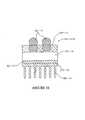
- the componentcomprises a semiconductor package in a chip scale configuration, and containing a single die having a circuit side, a back side and four edges.
- the dieincludes a semiconductor substrate thinned from the back side, and integrated circuits in a required configuration on the circuit side.
- the dieincludes die contacts on the circuit side in electrical communication with the integrated circuits,
- the componentincludes planarized contact bumps on the die contacts, and terminal contacts on the planarized contact bumps.
- the terminal contactscan comprise conductive bumps or balls, in a dense area array, such as a grid array, or alternately planar pads configured as an edge connector.
- the componentalso includes a circuit side polymer layer on the circuit side of the die encapsulating the planarized contact bumps, a back side polymer layer on the thinned back side of the die, and edge polymer layers on the edges of the die.
- a substratewhich contains a plurality of semiconductor dice having the die contacts formed thereon.
- the substratecan comprise a semiconductor wafer, or portion thereof, which contains dice separated by streets.
- conductive bumpsare formed on the die contacts using a suitable process, such as bonding pre-formed balls, electroless deposition, electrolytic deposition, or stenciling and reflowing of conductive bumps.
- Trenchesare then formed in the substrate between the dice to a depth that is less than a thickness of the substrate.
- the trenchescan be formed by scribing, etching or lasering the substrate.
- the circuit side polymer layeris then formed on the bumps and in the trenches, and both the circuit side polymer layer and the bumps can be planarized.
- the circuit side polymer layercan be formed using a nozzle deposition process, a transfer molding process, an injection molding process, a screen printing process, a stenciling process, a spin resist process, a dry film process, a stereo lithographic process, or any other suitable deposition process.
- the circuit side polymer layerprotects the dice during the fabrication process, and also protects the dice in the completed components.
- the substrateis thinned from the back side, such that the polymer filled trenches are exposed.
- the thinning stepcan be performed by mechanically planarizing the substrate or by etching the substrate.
- the back side polymer layeris formed on the thinned back side of the substrate and can also be planarized.
- the back side polymer layercan be formed as described above for the circuit side polymer layer.
- the back side polymer layerprotects the dice during the fabrication process, and also protects the dice in the completed components.
- the terminal contactsare formed on the contact bumps using a suitable deposition or bonding process.
- groovesare formed through the polymer filled trenches to singulate the completed components from one another.
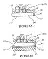
- the grooveshave a width that is less than the width of the polymer filled trenches, such that the edge polymer layers which comprise portions of the polymer filled trenches, remain on the four edges of the dice.
- the singulated componentis encapsulated on six sides (i.e., circuit side, back side, four edges) by the circuit side polymer layer, the back side polymer layer and by edge polymer layers on the four edges.
- the componentsPrior to the singulation step, the components can be tested and burned-in while they remain on the substrate.
- the componentsare electrically isolated on the substrate, which is a particular advantage for burn-in testing.
- a second embodiment componentincludes conductive vias in the thinned substrate, which electrically connect the die contacts to terminal contacts formed on the back side polymer layer.
- the terminal contactscan comprise conductive bumps or balls, or alternately planar pads configured as an edge connector.
- the conductive viascan be used to electrically connect terminal contacts on both sides of the component for stacking multiple components, and for facilitating testing of the components.
- a third embodiment componentis singulated by etching the substrate.
- the componentincludes a circuit side polymer layer, contact bumps embedded in the polymer layer, and terminal contacts on the contact bumps.
- the componentincludes a thin sealing coat, such as vapor deposited parylene, on five surfaces.
- a fourth embodiment componentincludes a circuit side polymer layer, contact bumps embedded in the polymer layer, and terminal contacts on the contact bumps.
- the componentincludes a thinned semiconductor substrate having a back side coat tape for protecting and laser marking the substrate.
- a heat sinkcan be attached directly to the back side of the thinned semiconductor substrate.
- a fifth embodiment componentincludes a circuit side polymer layer, which comprises two separate polymer materials, including an imageable polymer material (e.g., a photopolymer), and a second polymer material having tailored electrical characteristics.
- the imageable polymer materialalso covers the edges of the component, and is formed into dams having a criss-cross pattern configured to retain the tailored polymer material.
- the imageable polymer materialcan be blanket deposited, exposed, and then developed, using a conventional UV photolithography system, or alternately a laser stereo lithography system.
- a sixth embodiment pin grid array componentincludes conductive vias in a thinned die having conductive members in electrical communication with die contacts.
- a semiconductor substrate of the thinned diehas been planarized and etched to expose portions of the conductive members which form terminal contact pins for the component.
- a seventh embodiment componentincludes a thinned die having conductive vias formed by laser machining and etching openings in a thinned semiconductor substrate.
- the thinned substratecan include doped contacts, having a different conductivity type than the bulk of the substrate.
- the thinned substratecan be etched very thin, such that a very thin component is provided.
- An eighth embodiment ball grid array componentincludes conductive vias in a thinned die having conductive members in electrical communication with die contacts.
- a semiconductor substrate of the thinned diehas been planarized and etched to expose portions of the conductive members which are used to form a pattern of redistribution conductors.
- ballsare bonded to the redistribution conductors to form terminal contacts in a ball grid array.
- the componentscan be used to construct systems such as MCM packages, multi chip modules and circuit boards.
- the componentsprior to assembling the systems, the components can be tested at the wafer level, such that each of the components can be certified as a known good component (KGC) prior to incorporation into the system.
- KGCknown good component
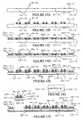
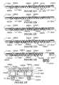
- FIG. 1Ais a schematic cross sectional view taken along section line 1 A— 1 A of FIG. 2A illustrating a step in a first embodiment fabrication method
- FIG. 1Bis a schematic cross sectional view taken along section line 1 B— 1 B of FIG. 2B illustrating a step in the first embodiment fabrication method
- FIG. 1Cis a schematic cross sectional view taken along section line 1 C— 1 C of FIG. 2C illustrating a step in the first embodiment fabrication method
- FIG. 1Dis a schematic cross sectional view taken along section line 1 D— 1 D of FIG. 2D illustrating a step in the first embodiment fabrication method
- FIG. 1Eis a schematic cross sectional view taken along section line 1 E— 1 E of FIG. 2E illustrating a step in the first embodiment fabrication method
- FIG. 1Fis a schematic cross sectional view taken along section line 1 F— 1 F of FIG. 2F illustrating a step in the first embodiment fabrication method
- FIG. 1Gis a schematic cross sectional view taken along section line 1 G— 1 G of FIG. 2G illustrating a step in the first embodiment fabrication method
- FIG. 1His a schematic cross sectional view taken along section line 1 H— 1 H of FIG. 2H illustrating a step in the first embodiment fabrication method
- FIG. 1Iis a schematic cross sectional view taken along section line 1 I— 1 I of FIG. 21 illustrating a step in the first embodiment fabrication method
- FIG. 1Jis a schematic cross sectional view taken along section line 1 J— 1 J of FIG. 2J illustrating a step in the first embodiment fabrication method
- FIG. 1Kis a schematic cross sectional view illustrating a step in the first embodiment fabrication method
- FIGS. 1L-1Nare schematic cross sectional views of an alternate embodiment of the first embodiment fabrication method shown in FIGS. 1A-1K ;
- FIG. 1Ois a schematic cross sectional view of an alternate embodiment of the first embodiment fabrication method shown in FIGS. 1A-1K ;
- FIGS. 1P-1Rare schematic cross sectional views of an alternate embodiment of the first embodiment fabrication method shown in FIGS. 1A-1K ;
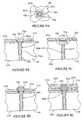
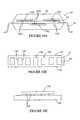
- FIG. 2Ais a cross sectional view taken along section line 2 A— 2 A of FIG. 1A illustrating die contacts on a wafer containing a plurality of semiconductor dice;
- FIG. 2Bis a cross sectional view taken along section line 2 B— 2 B of FIG. 1B illustrating bumps on the die contacts;
- FIG. 2Cis a cross sectional view taken along section line 2 C— 2 C of FIG. 1C illustrating trenches formed in the streets between the dice on the wafer;
- FIG. 2Dis a cross sectional view taken along section line 2 D— 2 D of FIG. 1D illustrating a good die dam on the wafer;
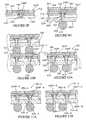
- FIG. 2Eis a cross sectional view taken along section line 2 E— 2 E of FIG. 1E illustrating a support dam on the wafer;
- FIG. 2Fis a cross sectional view taken along section lien 2 F— 2 F of FIG. 1F illustrating deposition of the circuit side polymer layer on the wafer;
- FIG. 2Gis a cross sectional view taken along section line 2 G— 2 G of FIG. 1G illustrating the circuit side polymer layer and the bumps following planarization;
- FIG. 2His a cross sectional view taken along section line 2 H— 2 H of FIG. 1H illustrating the polymer filled trenches on the back side of the wafer following back side thinning of the wafer;
- FIG. 2Iis a cross sectional view taken along section line 2 I— 2 I of FIG. 1I illustrating the back side polymer layer on the wafer following planarization;
- FIG. 2Jis a cross sectional view taken along section line 2 J— 2 J of FIG. 1J illustrating the terminal contacts on the circuit side polymer layer;
- FIG. 2Kis a cross sectional view taken along section line 2 K— 2 K of FIG. 1K illustrating the singulated first embodiment components and the edge polymer layers on the components;
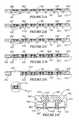
- FIG. 3Ais an enlarged portion of FIG. 2A illustrating a die contact
- FIG. 3Ban enlarged portion of FIG. 2B illustrating a metal bump
- FIG. 3Cis an enlarged portion of FIG. 2C illustrating the trenches in the streets of the wafer
- FIG. 3Dis an enlarged cross sectional view taken along section line 3 D— 3 D of FIG. 2D illustrating a metal bump, a trench and the good die dam;
- FIG. 3Eis an enlarged cross sectional view taken along section line 3 E— 3 E of FIG. 2E illustrating the support dam, the good die dam, a trench and two metal bumps;
- FIG. 3Fis an enlarged cross sectional view taken along section line 3 F— 3 F of FIG. 2F illustrating the circuit side polymer layer in the trenches and on the bumps;
- FIG. 3Gis an enlarged cross sectional view taken along section line 3 G— 3 G of FIG. 2G illustrating the circuit side polymer layer and the bumps following a planarization step;
- FIG. 3His an enlarged portion of FIG. 2H illustrating the polymer filled trenches following a back side thinning step
- FIG. 3Iis a cross sectional view taken along section line 3 I— 3 I of FIG. 2I illustrating the back side polymer layer on the wafer following a planarization step;
- FIG. 3Jis a cross sectional view taken along section line 3 J— 3 J of FIG. 2J illustrating the terminal contacts on the bumps and the circuit side polymer layer;
- FIG. 4Ais a plan view of a first embodiment semiconductor component
- FIG. 4Bis a side elevation view of FIG. 4A ;
- FIG. 4Cis an enlarged cross sectional view of the component taken along section line 4 C— 4 C of FIG. 4A ;
- FIG. 5Ais an enlarged cross sectional view equivalent to FIG. 4C of an alternate embodiment of the first embodiment component having planar terminal contacts configured as an edge connector;
- FIG. 5Bis a view taken along line 5 B— 5 B of FIG. 5A illustrating the edge connector
- FIG. 6Ais an enlarged cross sectional view equivalent to FIG. 4C of an alternate embodiment of the first embodiment component having encapsulation on five surfaces;
- FIG. 6Bis an enlarged cross sectional view equivalent to FIG. 4C of an alternate embodiment of the first embodiment component having a heat sink;
- FIG. 7is a block diagram illustrating steps in the first embodiment fabrication method
- FIGS. 8A-8Fare schematic cross sectional views illustrating steps in a second embodiment fabrication method
- FIGS. 8G-8Iare schematic cross sectional views illustrating steps in an alternate embodiment of the second embodiment fabrication method
- FIG. 9Ais an enlarged view taken along line 9 A— 9 A of FIG. 8A illustrating a conductive via
- FIG. 9Bis an enlarged cross sectional view taken along section line 9 B— 9 B of FIG. 8A illustrating the conductive via;
- FIG. 9Cis an enlarged cross sectional view equivalent to FIG. 9B but illustrating an alternate embodiment conductive via
- FIG. 9Dis an enlarged cross sectional view taken along section line 9 D— 9 D of FIG. 8B illustrating a contact bump on the conductive via;
- FIG. 9Eis an enlarged cross sectional view taken along section line 9 E— 9 E of FIG. 8C illustrating the conductive via, the contact bump, and a circuit side polymer layer prior to planarization;
- FIG. 9Fis an enlarged cross sectional view taken along section line 9 F— 9 F of FIG. 8D illustrating the conductive via, the contact bump, and the circuit side polymer layer following planarization;
- FIG. 9Gis an enlarged cross sectional view taken along section line 9 G— 9 G of FIG. 8E illustrating the conductive via, the contact bump, the circuit side polymer layer, a back side polymer layer, and a terminal contact in electrical communication with the conductive via;
- FIG. 9His an enlarged cross sectional view taken along section line 9 H— 9 H of FIG. 8H illustrating the conductive via, planarized contact bump and terminal contact formed using the fabrication method of FIGS. 8G-8I ;
- FIG. 10Ais an enlarged partial cross-sectional view illustrating a second embodiment component fabricated using the fabrication method of FIGS. 8A-8F ;
- FIG. 10Bis an enlarged partial cross sectional view t; illustrating two second embodiment components in a stacked assembly
- FIG. 11Ais an enlarged partial cross sectional view equivalent to FIG. 10A of an alternate embodiment of the second embodiment component having terminal contacts only on the back side polymer layer;
- FIG. 11Bis an enlarged partial cross sectional view equivalent to FIG. 10A of another alternate embodiment of the second embodiment component having offset terminal contacts;
- FIG. 11Cis an enlarged partial cross sectional view equivalent to FIG. 10A of another alternate embodiment of the second embodiment component having edge connector terminal contacts on the back side polymer layer;
- FIG. 11Dis an enlarged partial cross sectional view equivalent to FIG. 10A of another alternate embodiment of the second embodiment component having edge connector terminal contacts on both the back side polymer layer and the circuit side polymer layer;
- FIG. 11Eis an enlarged partial cross sectional view equivalent to FIG. 10A of another alternate embodiment of the second embodiment component having terminal contacts on the circuit side polymer layer;
- FIG. 11Fis an enlarged partial cross sectional view equivalent to FIG. 10A of another alternate embodiment of the second embodiment component having terminal contacts on both the circuit side polymer layer and the back side polymer layer;
- FIG. 12Ais an enlarged partial cross sectional view equivalent to FIG. 10A of another alternate embodiment of the second embodiment component configured as an interconnect;
- FIG. 12Bis an enlarged partial cross sectional view of a stacked system constructed using the interconnect component of FIG. 12A ;
- FIG. 12Cis an enlarged partial cross sectional view of a module system constructed using an alternate embodiment of the interconnect component of FIG. 12A ;
- FIGS. 13A-13Fare schematic cross sectional views illustrating steps in a method for fabricating a third embodiment semiconductor component using an etching step for singulating the component;
- FIG. 13Gis an enlarged cross sectional view taken along section line 13 G— 13 G of FIG. 13F illustrating a hermetic seal layer on the third embodiment component;
- FIG. 14Ais a cross sectional view taken along section line 14 A— 14 A of FIG. 13B illustrating an etch mask
- FIG. 14Bis a cross sectional view taken along section line 14 B— 14 B of FIG. 13C illustrating a circuit side polymer layer
- FIGS. 15A-15Fare schematic cross sectional views illustrating steps in a method for fabricating a fourth embodiment semiconductor component encapsulated on a single side;
- FIG. 15Gis an enlarged view taken along line 15 G— 15 G of FIG. 15E illustrating a laser marking
- FIG. 16is a schematic cross sectional view of an alternate embodiment of the fourth embodiment semiconductor component having a heat sink
- FIGS. 17A-17Iare schematic cross sectional views illustrating steps in a method for fabricating a fifth embodiment semiconductor component
- FIG. 17Jis an enlarged portion of FIG. 17I illustrating the fifth embodiment component.
- FIG. 18Ais a schematic cross sectional view of a system in a package (SIP) fabricated using components constructed in accordance with the invention
- FIG. 18Bis a plan view of a multi chip module system fabricated using components constructed in accordance with the invention.
- FIG. 18Cis a cross sectional view taken along section line 18 C— 18 C of FIG. 18B ;
- FIGS. 19A-19Fare schematic cross sectional views illustrating steps in a method for fabricating a sixth embodiment semiconductor component
- FIG. 19Gis an enlarged portion of FIG. 19F illustrating the completed sixth embodiment semiconductor component
- FIG. 20Ais a cross sectional view taken along section line 20 A— 20 A of FIG. 19A ;
- FIG. 20Bis a cross sectional view taken along section line 20 B— 20 B of FIG. 19B ;
- FIG. 20Cis a cross sectional view taken along section line 20 C— 20 C of FIG. 19C ;
- FIG. 20Dis a cross sectional view taken along section line 20 D— 20 D of FIG. 19D ;
- FIG. 20Eis a cross sectional view taken along section line 20 E— 20 E of FIG. 19E ;
- FIG. 20Fis a view taken along line 20 F— 20 F of FIG. 19F ;
- FIGS. 21A-21Eare schematic cross sectional views illustrating steps in a method for fabricating a seventh embodiment semiconductor component
- FIG. 21Fis an enlarged portion of FIG. 21E illustrating the completed seventh embodiment semiconductor component
- FIG. 21Gis an enlarged schematic cross section equivalent to FIG. 21F of an alternate embodiment of the seventh embodiment semiconductor component
- FIG. 21His an enlarged schematic cross section equivalent to FIG. 21F of an alternate embodiment of the seventh embodiment semiconductor component
- FIG. 21Iis an enlarged schematic cross section equivalent to FIG. 21F of an alternate embodiment of the seventh embodiment semiconductor component
- FIGS. 22A-22Eare schematic cross sectional views illustrating steps in a method for fabricating an eighth embodiment semiconductor component.
- FIG. 22Fis an enlarged portion of FIG. 22E illustrating the completed eighth embodiment semiconductor component.
- semiconductor componentrefers to an electronic element that includes a semiconductor die.
- Exemplary semiconductor componentsinclude semiconductor packages, semiconductor dice, BGA devices, and DDC devices.
- each completed component 16contains a single die encapsulated by polymer layers on six surfaces.
- the component 16is thus referred to as a “ 6 X component”.
- each die 10can comprise a dynamic random access memory (DRAM), a static random access memory (SRAM), a flash memory, a microprocessor, a digital signal processor (DSP) or an application specific integrated circuit (ASIC).
- DRAMdynamic random access memory
- SRAMstatic random access memory
- flash memorya flash memory
- microprocessordigital signal processor
- DSPdigital signal processor
- ASICapplication specific integrated circuit
- the dice 10 and the components 16can have any polygonal shape. In the illustrative embodiment, the dice 10 and the components 16 are rectangular in shape, but other polygonal shapes, such as square or hexagonal can also be utilized.
- the dice 10can be contained on a semiconductor wafer 12 .
- the methodis performed on an entire semiconductor wafer 12 , it is to be understood that the method can be performed on a portion of a wafer, on a panel, or on any other substrate that contains multiple semiconductor dice.
- the dice 10are formed on the wafer 12 with integrated circuits and semiconductor devices using techniques that are well known in the art. As also shown in FIG. 2A , the dice 10 are separated by streets 13 on the wafer 12 .
- the wafer 12 and each die 10includes a semiconductor substrate 14 wherein the integrated circuits are formed.
- the wafer 12 and each die 10include a circuit side 20 (first side) wherein the integrated circuits are located, and a back side 22 (second side).
- first sidethe integrated circuits
- back side 22second side
- the processes to followare described as being formed on the circuit side 20 or on the back side 22 , it is to be understood that any operation performed on the circuit side 20 can also be formed on the back side 22 , and any operation performed on the back side 22 can be performed on the circuit side 20 .
- Each die 10also includes a pattern of die contacts 18 formed on the circuit side 20 , in a dense area array, in electrical communication with the integrated circuits thereon.
- the die contacts 18are generally circular shaped metal pads having a desired size and spacing.
- the die contacts 18can comprise a solderable metal such as nickel, copper, gold, silver, platinum, palladium, tin, zinc and alloys of these metals.
- the die contacts 18comprise Ni/Au pads having a diameter of about 330 ⁇ m.
- the die contacts 18can be formed on the circuit side 20 of the wafer 12 using known techniques, such as deposition and patterning of one or more redistribution layers in electrical communication with the bond pads (not shown) for the dice 10 .
- known techniquessuch as deposition and patterning of one or more redistribution layers in electrical communication with the bond pads (not shown) for the dice 10 .
- the die contacts 18can comprise the bond pads of the dice 10 .
- the die contacts 18can be electrically insulated from the semiconductor substrate 14 by insulating layers (not shown), formed of suitable materials such as BPSG, SiO 2 or polyimide.
- a bump formation stepis performed in which contact bumps 24 are formed on the die contacts 18 .
- the contact bumps 24can comprise metal bumps deposited on the die contacts 18 using a suitable deposition process, such as stenciling and reflow of a solder alloy onto the die contacts 18 .
- the contact bumps 24can comprise solder, another metal, or a conductive polymer material.
- the contact bumps 24function as interconnects between the die contacts 18 and terminal contacts 42 ( FIG. 1K ) which will be formed on the completed components 16 .
- a dicing tape 26can be attached to the back side 22 of the wafer 12 for performing a scribing step to follow. Suitable dicing tapes 26 are manufactured by Furikawa or Nitto Denko.
- a scribing stepis performed, during which trenches 28 are formed in the streets 13 of the wafer 12 between the dice 10 .
- the scribing stepis illustrated after the bump formation step, it is to be understood that the scribing step can be performed prior to the bump formation step.
- the scribing stepcan be performed using a dicing saw having saw blades set to penetrate only part way through the wafer 12 .
- the scribing stepcan also be performed by etching the trenches 28 using a wet etching process, a dry etching process or a plasma etching process. With an etching process, the dicing tape 26 does not need to be employed. However, an etch mask (not shown) can be formed on the circuit side 20 of the wafer 12 having openings that define the pattern of the trenches 28 .
- the depth of the trenches 28can be controlled using suitable end pointing techniques.
- the trenches 28can be formed in the substrate 14 by laser machining the wafer 12 using a laser machining system.
- a suitable laser system for laser machining the trenches 28is manufactured by Electro Scientific, Inc., of Portland, Oreg. and is designated a Model No. 2700.
- the trenches 28can have a criss-cross pattern as shown, similar to a tic tac toe board, such that each trench is parallel to some trenches and perpendicular to other trenches. As such, the trenches 28 substantially surround each die 10 , defining the four edges 30 of each die 10 , and the rectangular polygonal peripheral shape of each die 10 as well.
- the trenches 28do not extend through the full thickness Tw of the wafer 12 and the semiconductor substrate 14 . Rather, the trenches 28 have a depth d measured from the surface of the circuit side 20 of the wafer 12 , that is less than the thickness Tw of the wafer 12 .
- the depth dcan have any value provided it is less than the value of the full thickness Tw.
- the depth dcan be from about 0.1 to 0.9 of the thickness Tw.
- the depth-dmust be greater than a depth Ts ( FIG. 3I ) of the thinned substrate 14 T ( FIG. 3I )
- the wafer 12has a thickness Tw of about 28 mils (725 ⁇ m), and the trenches 28 have a depth d of about 10 mils (254 ⁇ m). In addition to the depth d, the trenches 28 have a width W, which in the illustrative embodiment is about 4 mils (101.6 ⁇ m).
- the scribing stepcan be performed using a dicing saw having saw blades with the width W, which are configured to penetrate the circuit side 20 of the wafer 12 to the depth d. Alternately, with an etching process for forming the trenches 28 , openings in an etch mask determine the width W, and control of the etch process end points the trenches 28 with the depth d.
- a good die dam 32is formed on the circuit side 20 of the wafer 12 .
- the good die dam 32encircles only the complete, or “good” dice on the wafer. The incomplete or “bad” dice are not encircled by the good die dam 32 .
- the good die dam 32has a height H measured from the surface of the circuit side 20 of the wafer 12 that can be greater than, or alternately less than, a height Hb of the contact bumps 24 .
- the height Hb of the contact bumps 24is about 13.78 mils (350 ⁇ m), and the height H of the good die dam 32 is slightly greater.
- the good die dam 32can comprise a polymer material deposited on the wafer 12 using a suitable deposition process such as deposition through a nozzle, screen printing, stenciling or stereographic lithography.
- the good die dam 32is deposited on the wafer 12 using a nozzle deposition apparatus.
- the nozzle deposition apparatusis under computer control, and is configured to move in x and y directions across the wafer 12 , and in z directions towards and away from the wafer 12 .
- One suitable nozzle deposition apparatusalso known as a material dispensing system, is manufactured by Asymtek of Carlsbad, Calif.
- the good die dam 32can comprise a curable polymer material having a relatively high viscosity, such that the polymer material sticks to the wafer 12 , and stays in a desired location.
- Suitable curable polymers for the good die dam 32include silicones, polyimides and epoxies.
- these polymer materialscan include fillers such as silicates configured to reduce the coefficient of thermal expansion (CTE) and adjust the viscosity of the polymer material.
- CTEcoefficient of thermal expansion
- One suitable curable polymeris manufactured by Dexter Electronic Materials of Rocky Hill, Conn. under the trademark “HYSOL” FP4451.
- the good die dam 32can also comprise a polymer such as parylene, deposited using a vapor deposition process to be hereinafter described.
- a support dam 34is formed on the wafer 12 .
- the support dam 34comprises a serpentine-shaped ribbon of polymer material formed outside of the good die dam 32 proximate to the peripheral edges of the wafer 12 .
- the support dam 34is configured to support peripheral areas of the wafer 12 during the planarization steps to follow. Specifically, these peripheral areas are subject to cracking without the support dam 34 .
- the support dam 34can comprise a curable polymer material deposited using a suitable deposition process such as deposition through a nozzle, screen printing or stenciling.
- the support dam 34comprises a same material as the good die dam 32 , and is deposited using the previously described nozzle deposition apparatus.
- the support dam 34can comprise one or more pre-formed polymer elements attached to the wafer 12 .
- the support dam 32can have a serpentine-shape, a donut shape, or can merely be a segment or ribbon of material, that supports a particular area on the wafer 12 .
- both the good die dam 32 and the support dam 34can be cured to harden the polymer material.
- curingcan be performed by placing the wafer 12 in an oven at a temperature of about 90° to 165° C. for about 30 to 60 minutes.
- a circuit side polymer layer 36is deposited on the circuit side 20 of the wafer 12 within the good die dam 32 .
- the circuit side polymer layer 36can comprise a relatively low viscosity, curable material configured to spread over a relatively large area.
- the circuit side polymer layer 36can be deposited using a suitable deposition process such as deposition through a nozzle, spatuling, screen printing or stenciling.
- the circuit side polymer layer 36is deposited in a spiral pattern 46 ( FIG. 2F ) to completely fill the area enclosed by the good die dam 32 , using the previously described nozzle deposition apparatus.
- the circuit side polymer layer 36is contained by the good die dam 32 .
- the circuit side polymer layer 36encapsulates the contact bumps 24 and covers the surfaces of the dice 10 .
- the circuit side polymer layer 36fills the trenches 28 , forming polymer filled trenches 28 P between the dice 10 .
- the circuit side polymer layer 36can comprise a curable polymer such as a silicone, a polyimide or an epoxy.
- these materialscan include fillers, such as silicates, configured to reduce the coefficient of thermal expansion (CTE) and adjust the viscosity of the polymer material.
- a curable polymer materialis manufactured by Dexter Electronic Materials of Rocky Hill, Conn. under the trademark “HYSOL” FP4450.
- the circuit side polymer layer 36can be cured to harden the polymer material.
- curingcan be performed by placement of the wafer 12 in an oven at a temperature of about 90° to 165° C. for about 30 to 60 minutes.
- a circuit side planarization stepis performed, in which the circuit side polymer layer 36 is planarized to form a planarized circuit side polymer layer 36 P.
- This planarization stepalso planarizes the contact bumps 24 to form planarized contact bumps 24 P.
- this planarization stepplanarizes the good die dam 32 to form a planarized good die dam 32 P, and planarizes the support dam 34 to form a planarized support dam 34 P.
- the circuit side planarization stepcan be performed using a mechanical planarization apparatus (e.g., a grinder).
- a mechanical planarization apparatuse.g., a grinder
- One suitable mechanical planarization apparatusis manufactured by Okamoto, and is designated a model no. VG502.
- the circuit side planarization stepcan also be performed using a chemical mechanical planarization (CMP) apparatus.
- CMPchemical mechanical planarization
- a suitable CMP apparatusis commercially available from a manufacturer such as Westech, SEZ, Plasma Polishing Systems, or TRUSI.
- the circuit side planarization stepcan also be performed using an etch back process, such as a wet etch process, a dry etch process or a plasma etching process.
- the circuit side planarization stepcan be performed such that the thickness of the circuit side polymer layer 36 is reduced by an amount sufficient to expose and planarize the surfaces of the contact bumps 24 .
- the planarized circuit side polymer layer 24 Phas a thickness Tcs of about 12 mils (304.8 ⁇ m).
- the circuit side planarization stepneed not also planarize the contact bumps 24 .
- the contact bumps 24can remain generally concave in shape, and can protrude past the surface of the planarized circuit side polymer layer 36 P.
- the circuit side polymer layer 36can be formed by another suitable deposition process, such as an injection molding process, a transfer molding process, a stenciling process, a screen printing process, a spin resist process, a ft dry film process, or a stereographic lithographic process.
- the circuit side polymer layer 36can comprise a polymer such as parylene, deposited using a vapor deposition process to be hereinafter described.
- the circuit side polymer layer 36can comprise a wafer level underfill material to be hereinafter described.
- a back side thinning stepis performed using the above described mechanical planarization apparatus.
- the back side thinning stepremoves semiconductor material from the semiconductor substrate 14 to form a thinned semiconductor substrate 14 T and thinned dice 10 T.
- enough of the semiconductor materialis removed to expose the polymer filled trenches 28 P.
- the back side thinning stepwould singulate the thinned dice 10 T, but the polymer filled trenches 28 P hold the thinned dice 10 T and the wafer 12 together.
- all of the thinned dice 10 Tare electrically isolated by the polymer filled trenches 28 P.
- the amount of semiconductor material removed by the back side thinning stepis dependent on the thickness Tw of the wafer 12 , and on the depth d of the trenches 28 .
- the thickness Tw of the wafer 12is about 28 mils (725 ⁇ m)
- the depth d of the trenchesis about 10 mils (25.4 ⁇ m)
- at least 18 mils (457.2 ⁇ m) of semiconductor materialmust be removed to expose the polymer filled trenches 28 P.
- about 22 mils (558.8 ⁇ m) of semiconductor materialis removed, such that the thickness Ts ( FIG. 3I ) of the thinned substrate 14 T is about 6 mils (152.4 ⁇ m).
- the thickness Ts of the thinned substrate 14 Tcan vary from about 10 ⁇ m to 720 ⁇ m.
- a chemical polishing stepcan be performed to remove grind damage to the thinned semiconductor substrate 14 T.
- Polishingcan be performed using a commercial CMP apparatus from a manufacturer such as Westech, SEZ, Plasma Polishing Systems or TRUSI.
- an etching stepcan be performed using an etchant such as TMAH, to remove grind damage to the thinned semiconductor substrate 14 T.
- a planarized back side polymer layer 38 Pis formed on the thinned back side 22 T of the thinned wafer 12 T.
- the planarized back side polymer layer 38 Pcan be formed by depositing a polymer material on the thinned back side 22 T, curing the polymer material, and then mechanically planarizing the cured polymer material. All of these steps can be performed substantially as previously described for the planarized circuit side polymer layer 36 P.
- the planarized back side polymer layer 38 Pcan be formed by attaching or laminating a polymer film, such as a polyimide or epoxy tape, having an adhesive surface and a desired thickness to the thinned back side 22 T. In this case the back side planarizing step can be eliminated.
- a polymer filmsuch as a polyimide or epoxy tape
- One suitable polymer filmis a polymer tape manufactured by Lintec, and designated #LE 5950.
- the back side polymer layer 38 Pcan be formed by an injection molding process, a transfer molding process, a spin resist process, a dry film process, a stereo lithographic process, or any other suitable process.
- a thickness T of the component 16is equal to a thickness Tp of the planarized back side polymer layer 38 P, plus the thickness Ts of the thinned fill substrate 14 T.
- the polymer materialis initially deposited to a thickness of about 12 mils, and the thickness Tp of the planarized back side polymer layer 38 P is about 10.5 mils (266.7 ⁇ m). Accordingly, the thickness T of the component 16 is about 28.5 mils (723.9 ⁇ m).
- pin one indicatorscan be laser printed on the back side polymer layer 38 P, and also on the circuit side polymer layer 36 P, as required.
- This printing stepcan be performed using a conventional laser printing apparatus.
- the planarized back side polymer layer 38 Pis opaque to the wavelength of the laser being employed during the printing step.
- a terminal contact forming stepis performed for forming the terminal contacts 42 .
- This stepis performed by bonding, or depositing, the terminal contacts 42 on the planarized surface of the planarized contact bumps 24 P.
- the terminal contacts 42can comprise metal bumps deposited on the planarized contact bumps 24 P using a suitable deposition process, such as stenciling and reflow of a solder alloy. If desired, the same stencil mask that was used to form the contact bumps 24 P can be used to form the terminal contacts 42 .
- the terminal contacts 42can comprise another metal, or a conductive polymer material.
- the terminal contacts 42can also be formed by electrolytic deposition, by electroless deposition, or by bonding pre-fabricated balls to the planarized contact bumps 24 P.
- a ball bumpercan also be employed to bond pre-fabricated balls.
- a suitable ball bumperis manufactured by Pac Tech Packaging Technologies of Falkensee, Germany.
- the terminal contacts 42can also be formed using a conventional wire bonder apparatus adapted to form a ball bond, and then to sever the attached wire.
- the terminal contacts 42are in effect “stacked” on the planarized contact bumps 24 P, a relatively large spacing distance is provided for flip chip mounting, and the reliability of the component 16 is increased.
- the offset, or spacing, provided by the planarized contact bumps 24 P and the terminal contacts 42may allow the component 16 to be flip chip mounted without requiring an underfill for some applications.
- the terminal contacts 42can be rigidified with a polymer support layer as described in U.S. Pat. No. 6,180,504 B1 to Farnworth et al., which is incorporated herein by reference.
- the terminal contacts 42can be formed in a standardized grid array as described in U.S. Pat. No. 6,169,329 to Farnworth et al., which is incorporated herein by reference.
- the terminal contacts 42can be formed as described in U.S. Pat. No. 6,281,131 B1 to Gilton et al., which is incorporated herein by reference.
- a representative diameter Dcan be from about 0.005-in (0.127 mm) to about 0.016-in (0.400 mm) or larger.
- a representative pitch Pcan be from about 0.004-in (0.100 mm) to about 0.039 in (1.0) mm or more.
- the dicing tape 26can be applied to the planarized back side polymer layer 38 P.
- a singulating stepis performed to singulate the components 16 from the wafer 12 and from one another.
- grooves 44are sawn, or otherwise formed, in the polymer filled trenches 28 P.
- the grooves 44extend through the planarized circuit side polymer layer 36 P, through the polymer filled trenches 28 P, through the planarized back side polymer layer 38 P, and into the dicing tape 26 .
- the grooves 44have a width Wg that is less than the width W of the trenches 28 . Accordingly, edge polymer layers 40 remain on the four edges 30 of the thinned die 10 T.
- the edge polymer layers 40comprise portions of the polymer material in the polymer filled trenches 28 P. Further, the edge polymer layers 40 provide rigidity for the edges of the component 16 , and for the terminal contacts 42 proximate to the edges of the component 16 .
- the singulating stepcan be performed using a dicing saw having saw blades with the width Wg. Alternately the singulating step can be performed using another singulation method, such as cutting with a laser or a water jet or be etching the substrate 14 T with a suitable wet or dry etchant.
- the width of the trenches 28is about 4 mils (101.6 ⁇ m)
- the width Wg of the grooves 44is about 2 mils (50.8 ⁇ m)
- the edge polymer layers 40will have a thickness of about 1 mil (25.4 ⁇ m).
- the components 16 on the wafer 12can be tested and burned-in using a wafer level test process.
- Suitable wafer level burn-in test proceduresare described in U.S. Pat. No. 6,233,185 B1 to Beffa et al., which is incorporated herein by reference.
- a wafer level burn-in apparatusis described in U.S. Pat. No. 6,087,845 to Wood et al., which is incorporated herein by reference.
- the components 16 on the wafer 12are electrically isolated by the polymer filled trenches 28 P and the back side planarization step, burn-in testing is improved, as defective components 16 remain electrically isolated, and do not adversely affect the burn-in test procedure.
- the active circuitry on the thinned semiconductor die 10 Tis protected from damage during test and burn-in.
- the components 16have a physical robustness that facilitates testing and handling of the components 16 by the manufacturer and the end user.
- the component 16includes the thinned die 10 T, the thinned substrate 14 T and the die contacts 18 in electrical communication with the integrated circuits thereon.
- the component 16also includes the planarized contact bumps 24 P on the die contacts 18 .
- the component 16includes the planarized circuit side polymer layer 36 P which covers the circuit side 20 of the thinned die 14 T, and encapsulates the planarized contact bumps 24 P.
- the planarized contact bumps 24 Pare thus supported and rigidified by the planarized circuit side polymer layer 36 P.
- the planarized contact bumps 24 Pfunction as interconnects between the die contacts 18 and the terminal contacts 42 .
- the planarized circuit side polymer layer 36 Phas been mechanically planarized to a precise thickness with a planar surface.
- the component 16also includes the terminal contacts 42 bonded to the planarized contact bumps 24 P.
- the terminal contacts 42are arranged in a dense area array such as a ball grid array (BGA), such that a high input/output capability is provided for the component 16 .
- BGAball grid array
- the component 16also includes the planarized back side polymer layer 38 P which covers the thinned back side 22 T of the thinned die 10 T.
- the planarized back side polymer layer 38 Phas been mechanically planarized to a precise thickness with a planar surface.
- the component 16includes four edge polymer layers 40 which cover and rigidify the four edges 30 of the thinned die 10 T.
- the component 16is thus protected on six sides by polymer layers 36 P, 38 P and 40 .
- the planarized circuit side polymer layer 36 P and the edge polymer layers 40are a continuous layer of material, and the planarized back side polymer layer 38 P is a separate layer of material.
- the edge polymer layers 40are formed by portions of the polymer filled trenches 28 P (FIG. 3 F).
- an alternate embodiment component 16 ECis substantially similar to the previously described component 16 ( FIGS. 4A-4C ) but includes terminal contacts 42 EC configured as an edge connector 43 (FIG. 5 B).
- the edge connector 43( FIG. 5B ) can be configured as described in U.S. Pat. No. 5,138,434 to Wood et al., which is incorporated herein by reference.
- the terminal contacts 42 ECcan comprise planar, polygonal pads formed of a relatively hard metal such as copper or nickel.
- conductors 45 on the circuit side 20establish electrical paths between the terminal contacts 42 EC and the die contacts 18 .
- the component 16 ECcan be fabricated substantially as shown in FIGS. 1A-1K , but with the conductors 45 and the terminal contacts 42 EC fabricated in place of the contact bumps 24 .
- the conductors 45 and the terminal contacts 42 ECcan be fabricated by deposition and patterning of one or more metal layers. Alternately electroless plating can provide robustness and lower electrical resistance.
- an alternate embodiment component 16 - 5 Xis substantially similar to the previously described component 16 ( FIGS. 4A-4C ) but is encapsulated on five surfaces rather than on six surfaces.
- the component 16 - 5 Xdoes not include a polymer layer on the thinned backside 22 T of the thinned semiconductor substrate 14 T.
- the thinned backside 22 Tis thus exposed, and can be used to mount a heat sink to the thinned semiconductor substrate 14 T.
- the component 16 - 5 ⁇can be fabricated essentially as shown in FIGS. 1A-1K , but without forming the planarized back side polymer layer 38 P of FIG. 1 I.
- an alternate embodiment component 16 HSis substantially similar to the previously described component 16 - 5 ⁇ (FIG. 4 F), but includes a heat sink 65 attached to the thinned back side 22 T of the thinned semiconductor substrate 14 T.
- a thermally conductive adhesive layer 63such as a nitride filled epoxy, attaches the heat sink 65 to the thinned back side 22 T. Heat transfer between the thinned semiconductor substrate 14 T and the heat sink 65 is facilitated because the thinned back side 22 T exposes the semiconductor material.
- the heat sink 65can comprise a flat metal plate formed of copper or other metal having a high thermal conductivity.
- the heat sink 65can include ribs or fins (not shown) configured to provide an increased surface area for heat transfer.
- FIG. 7summarizes the steps illustrated in FIGS. 1A-1K for fabricating the first embodiment component 16 .
- FIGS. 1L-1Nan alternate embodiment of the first embodiment fabrication method illustrated in FIGS. 1A-1K is illustrated.
- the same stepsare utilized as previously shown in FIGS. 1A-1G and described in the related portions of the specification.
- the thinning stepis performed as shown in FIG. 1L , by mechanical planarization in combination with etching to remove damage caused by the mechanical planarization.
- Thisforms a thinned wafer 12 T-E having thinned dice 10 T-E with thinned substrates 14 T-E, substantially as previously described.
- the polymer filled trenches 28 P-Eextend past the thinned back side 22 T-E because they are not affected by the etching process.
- the thinned semiconductor substrates 14 T-Eare recessed with respect to the back side edges of the polymer filled trenches 28 P-E.
- the etching processcan be performed using a wet etchant, such as KOH or TMAH, that selectively etches the semiconductor substrate 14 .
- the etching processcan be performed using a dry etching process or a plasma etching process.
- the polymer filled trenches 28 P-Ecan be polished back to the level of the thinned back side 22 T-E.
- planarized back side polymer layers 38 P-Eare formed on the thinned substrates 14 T-E, substantially as previously described for planarized back side polymer layer 38 P.
- the planarized back side polymer layers 38 P-Efit into the recesses formed by the polymer filled trenches 28 P-E.
- each singulated component 16 -Eincludes a thinned die 10 T-E that has been etched back from the back side.
- each component 16 -Eincludes the planarized back side polymer layer 38 P-E, and edge polymer layers 40 E which comprise portions of the polymer filled trenches 28 P-E.
- FIG. 10corresponds to FIG. 1N which shows the singulating step. All of the previous fabrication steps as shown in FIGS. 1A-1J are the same. However, in this embodiment the singulating step is performed as shown in FIG. 10 , such that singulated components 16-BE have beveled edges 51 .
- the beveled edges 51can be formed using saw blades configured to make beveled cuts.
- FIGS. 1P-1Ran alternate embodiment of the first embodiment fabrication method illustrated in FIGS. 1A-1K is illustrated.
- this methodthe same steps are utilized as previously shown in FIGS. 1A-1G and described in the related portions of the specification.
- both a circuit side polymer layer 36 UF, and a back side polymer layer 38 UFcomprise a polymer film having specific characteristics.
- the polymer filmcomprises a thermoset polymer film having a Young's modulus of about 4G Pascal, and a coefficient of thermal expansion (CTE) of about 33 parts per million per ° C.
- the polymer filmpreferably cures and planarizes at a temperature and in a time period that are similar to the temperature and time period for a solder reflow process for bonding solder bumps to semiconductor components (e.g., about 200-250° C. for about several minutes).
- the polymer filmpreferably has low alpha emission characteristics.
- thermoset polymer filmis a wafer level underfill film manufactured by 3M corporation.
- this polymer filmis self planarizing, such that a mechanical planarization step as previously described is not necessary.
- the wafer 12 UFhas a back side 22 UF, and includes semiconductor dice 10 UF on a semiconductor substrate 14 UF.
- contact bumps 24 UFhave been formed on die contacts 18 UF substantially as previously described for contact bumps 24 ( FIG. 1B ) and die contacts 18 (FIG. 1 A).
- a circuit side polymer layer 36 UFis formed by depositing and curing the above described thermoset polymer film on the circuit side 20 UF of the wafer 12 UF.
- a piece of the polymer film having a desired thickness, and about the same peripheral shape as the wafer 12 UFis placed on the circuit side 20 UF and on the contact bumps 24 UF.
- the polymer filmis then heated to a temperature of about 200-250° C. for several minutes, such that softening and then curing occurs.
- each contact bump 24 UFis surrounded by a portion of the circuit side polymer layer 36 UF, but with a tip portion of each contact bumps 24 UF exposed.
- the circuit side polymer layer 36 UFhas a thickness Tuf on the circuit side 20 UF that is less than a height Hcb of the contact bumps 24 UF.
- the thickness Tufis about half the height Hcb.
- the thickness Tufcan be from about 0.1 to 0.9 of the height Hcb.
- Polymer filled trenches 28 UFare also formed during formation of the circuit side polymer layer 36 UF, substantially as previously described for polymer filled trenches 28 P (FIG. 1 F). In this case, during the curing step the above described polymer film softens and flows into the trenches 28 (FIG. 1 C).
- a thinning stepis performed substantially as previously described, to form a thinned wafer 12 T-UF having thinned dice 10 T-UF and a thinned substrate 14 T-UF with a thinned back side 22 T-UF.
- a back side polymer layer 38 UFis formed on the thinned back side 22 T-UF by depositing and curing the above described polymer film.
- the back side polymer layer 38 UFcan be formed using the previously described deposition and planarization steps.
- each singulated component 16 UFincludes a thinned die 10 T-UF.
- each singulated component 16 UFincludes a portion of the circuit side polymer layer 36 UF, a portion of the back side polymer layer 38 UF, and edge polymer layers 40 UF which comprise portions of the polymer filled trenches 28 UF.
- each component 16 UFincludes exposed contact bumps 24 UF, which function as the terminal contacts for the component 16 UF.
- the contact bumps 24 UFare rigidified by the circuit side polymer layer 36 UF.
- terminal contactscan be bonded to the exposed contact bumps 24 UF, as previously described for terminal contacts 42 (FIG. 1 K).
- each completed component 16 Aincludes a single semiconductor die encapsulated on six surfaces (6 ⁇ ).
- each dieincludes conductive vias 68 A formed in a semiconducting substrate thereof.
- each die 10 Aincludes a semiconductor substrate 14 A containing integrated circuits.
- the wafer 12 A and each die 10 Aincludes a circuit side 20 A (first side) wherein the integrated circuits are located, and a back side 22 A (second side).
- Each die 10 Aalso includes a pattern of die contacts 18 A in the form of bond pads on the circuit side 20 A, in electrical communication with the integrated circuits thereon.
- the die contacts 18 Aare embedded in an insulating layer 64 A having openings 80 A aligned with the die contacts 18 A.
- the insulating layer 64 Acan comprise a glass such as BPSG, an oxide such as silicon dioxide, or a polymer layer such as polyimide.
- a dielectric layer 71 Aelectrically insulates the die contacts 18 A from the bulk of the substrate 14 A, and from the integrated circuits on the substrate 14 A.
- the dielectric layer 71 Acan comprise an electrically insulating material such as silicon dioxide, or polyimide, formed during fabrication of the wafer 12 A.
- the dielectric layer 71 Arather than being blanket deposited, can be located or can have a shape (e.g., donut shape) that insulates only selected portions of the substrate 14 A.
- each conductive via 68 Aincludes a via 74 A formed in the substrate 14 A, a conductive member 76 A in the via 74 A, and an insulating layer 78 A which electrically insulates the conductive member 76 A from the bulk of the substrate 14 A.
- openings 82 Aare formed in the die contacts 18 A using an etch mask (not shown) and an etching process.
- a wet etchantcan be used to etch the die contacts 18 A.
- one suitable wet etchantis H 3 PO 4 .
- the openings 82 A in the die contacts 18 Aare generally circular, and are smaller in diameter than the width of the die contacts 18 A. The die contacts 18 A thus have metal around their peripheries, but no metal in the center.
- the openings 82 Ahave a diameter that is about one half the width of the die contacts 18 A.
- the openings 82 Asurround a portion of the substrate 14 A, such that the die contacts 18 A and the openings 82 A form targets, or bullseyes, for a subsequent laser drilling step in which a laser beam is directed at the openings 82 A and through the substrate 14 A.
- the laser beaminitially pierces the substrate 14 A on the portions of the substrate 14 A surrounded by the openings 82 A.
- the laser drilling stepforms lasered openings through the substrate 14 A, which do not touch the metal of the die contacts 18 A, as they are located in the middle of the openings 82 A in the die contacts 18 A.
- the lasered openingscan have diameters that are about one half the diameter of the openings 82 A.
- the laser beamthus initially contacts and pierces the substrate 14 A without having to contact and pierce the metal that forms the die contacts 18 A. This helps to prevent shorting between the conductive via and the die contacts 18 A.
- a cleaning stepcan be performed in which the lasered openings are cleaned using a suitable wet or dry etchant to form the vias 74 A for the conductive vias 68 A.
- a suitable wet or dry etchantfor cleaning the lasered openings with the substrate 14 A comprising silicon is tetramethylammoniumhydroxide (TMAH).
- TMAHtetramethylammoniumhydroxide
- the diameters of the vias 74 Acan be from 10 ⁇ m to 2 mils or greater.
- a suitable laser system for performing the laser drilling stepis manufactured by Electro Scientific, Inc., of Portland, Oreg. and is designated a Model No. 2700.
- a representative laser fluence for forming the vias 74 A through a silicon substrate having a thickness of about 28 mils,is from 2 to 10 watts/per opening at a pulse duration of 20-25 ns, and at a repetition rate of up to several thousand per second.
- the wavelength of the laser beamcan be a standard UV wavelength (e.g., 355 nm).
- the insulating layers 78 Acan be formed on the inside surfaces of the vias 74 A.
- the insulating layers 78 Acan be a grown or a deposited material.
- the insulating layers 78 Acan be an oxide, such as SiO 2 , formed by a growth process by exposure of the substrate 14 A to an O 2 atmosphere at an elevated temperature (e.g., 950° C.). In this case the insulating layers 78 A do not completely close the vias 74 A, but form only on the sidewalls of the vias 74 A.
- the insulating layers 78 Acan comprise an electrically insulating material, such as an oxide or a nitride, deposited using a deposition process such as CVD, or a polymer material deposited using a suitable deposition process such as screen printing.
- an electrically insulating materialsuch as an oxide or a nitride
- CVDchemical vapor deposition
- a polymer materialdeposited using a suitable deposition process such as screen printing.
- the conductive members 76 Acan be formed within the vias 74 A.
- the conductive members 76 Acan be plugs that completely fill the vias 74 A, or alternately, can be layers that cover just the inside surfaces or sidewalls of the vias 74 A.
- the conductive members 76 Acan comprise a highly conductive metal, such as aluminum, titanium, nickel, iridium, copper, gold, tungsten, silver, platinum, palladium, tantalum, molybdenum, tin, zinc and alloys of these metals.
- the above metalscan be deposited within the openings 76 A using a deposition process, such as electroless deposition, CVD, or electrolytic deposition.
- a solder metalcan be screen printed in the vias 74 A and drawn into the vias 74 A with capillary action. A solder metal can also be drawn into the vias 74 A using a vacuum system and a hot solder wave.
- the conductive members 76 Acan comprise a conductive polymer, such as a metal filled silicone, or an isotropic epoxy. Suitable conductive polymers are available from A.I. Technology, Trenton, N.J.; Sheldahl, Northfield, Minn.; and 3 M, St. Paul, Minn. A conductive polymer can be deposited within the vias 74 A, as a viscous material, and then cured as required. A suitable deposition process, such as screen printing, or stenciling, can be used to deposit the conductive polymer into the vias 74 A.
- a conductive polymersuch as a metal filled silicone, or an isotropic epoxy.
- Suitable conductive polymersare available from A.I. Technology, Trenton, N.J.; Sheldahl, Northfield, Minn.; and 3 M, St. Paul, Minn.
- a conductive polymercan be deposited within the vias 74 A, as a viscous material, and then cured as required.
- the conductive vias 68 Acan also be formed using the laser machining processes disclosed in U.S. Pat. No. 6,107,109 to Akram et al, U.S. Pat. No. 6,114,240 to Akram et al., and U.S. Pat. No. 6,294,837 B1 to Akram et al., all of which are incorporated herein by reference. Rather than a laser machining processes, the conductive vias 68 A can be formed by etching the vias 74 A using an etch mask and a suitable etchant. As another alternative, the conductive vias 68 A can be formed as described in U.S. Pat. No. 6,313,531 B1 to Geusic et al., which is incorporated herein by reference.
- an alternate embodiment counter bored conductive via 68 A-CBcan be formed in the substrate 14 A.
- the above described laser machining processcan be controlled to form the counter bored conductive via 68 A-CB from the backside 22 A but only part way through the substrate 14 A.
- the substrate 14 Acan be a first conductivity type (e.g., P type silicon).
- the substrate 14 Acan include a conductivity region 114 A for each counterbored via 68 A-CB having a second conductivity type (e.g., N type silicon).
- the conductivity region 114 Acan comprise a portion of the substrate 14 doped to provide a conductivity type that is opposite to that of the substrate 14 A.
- the conductivity region 114 Acan comprise N type silicon, while the bulk of the substrate 14 A can comprise P type silicon.
- the conductivity region 114 Acan be doped with phosphorus or arsenic or any other suitable dopant, while the bulk of the substrate 14 A can be doped with boron or gallium or any other suitable dopant.
- This arrangementallows some latitude in locating the counterbored via 68 A-CB because a reverse bias junction is formed by the conductivity region 114 A, and an additional insulating layer is not required in the area of the conductivity region 114 A.
- the terminal contact 42 A( FIG. 8F ) can be formed directly on the conductivity region 114 A such that a tolerance equal to the height of the conductivity region 114 A is provided for locating the counterbored via 68 A-CB.
- contact bumps 24 Aare formed on the die contacts 18 A in electrical communication with the conductive vias 68 A.
- the contact bumps 24 Acan comprise a solderable metal such as nickel, copper, gold, silver, platinum, palladium or alloys of these metals. These metals can be deposited using an electroless or electrolytic deposition process in a manner similar to deposition of a conventional under bump metalization layer.
- the contact bumps 24 Afill the openings 80 A in the insulating layer 64 A, fill the openings 82 A in the die contacts 18 A, and physically contact the conductive members 76 A.
- the contact bumps 24 Acan be used to stack multiple components 16 A and to provide contact points for testing the components 16 A.
- trenches 28 Aare formed part way through the substrate 14 A using a scribing, etching or lasering process, substantially as previously described.
- a circuit side polymer layer 36 Acan be formed on the circuit side 20 A and on the contact bumps 24 A.
- the circuit side polymer layer 36 Acan be formed substantially as previously described for circuit side polymer layer 36 in FIG. 1 F.
- the circuit side polymer layer 36 A and the contact bumps 24 Acan be mechanically planarized (ground) to form a planarized circuit side polymer layer 36 AP and planarized contact bumps 24 AP.
- This planarization stepcan be performed substantially as previously described for circuit side polymer layer 36 and planarized contact bumps 24 P in FIG. 1 G.
- the metal material of the contact bumps 24 Aprovides a contact surface for end pointing the planarization process.
- a backside thinning stepis performed, as previously described and shown in FIG. 1H to form a thinned substrate 14 AT having a thinned back side 22 AT.
- a planarized back side polymer layer 38 APis formed on the thinned back side 22 AT of the thinned substrate 14 AT.
- This stepcan be formed by depositing a polymer material on the thinned back side 22 AT, curing the polymer material, and then mechanically planarizing the cured polymer material, substantially as previously described and shown in FIG. 1I for planarized back side polymer layer 38 P.
- the planarized back side polymer layer 38 APcan be formed by attaching or laminating a polymer film, such as a polyimide or epoxy tape, having an adhesive surface and a desired thickness to the thinned back side 22 AT.
- planarized back side polymer layer 38 APcan comprise a polymer film that is opaque to radiation at a selected wavelength. Such an opaque material will prevent damage to the integrated circuits on the thinned substrate 14 AT during subsequent processing, such as laser marking with a laser beam at the selected wavelength.
- the planarized back side polymer layer 38 APcan also comprise a photoimageable polymer material, such as a thick film resist.
- a photoimageable polymer materialsuch as a thick film resist.
- One such resistcomprises a negative tone resist, which is blanket deposited to a desired thickness, exposed, developed and then cured.
- a suitable resist formulationis sold by Shell Chemical under the trademark “EPON RESIN SU- 8 ”.
- Such a resistcan be deposited to a thickness of from about 0.5-20 mils and then built up using successive layers.
- a conventional resist coating apparatus, such as a spin coater, or a meniscus coatercan be used to deposit the resist. The deposited resist can then be “prebaked” at about 95° C.
- Developingcan be accomplished with a solution of PGMEA (propylenglycol-monomethylether-acetate) This can be followed by a hard bake at about 200° C. for about 30 minutes.
- PGMEApropylenglycol-monomethylether-acetate
- the planarized back side polymer layer 38 APincludes conductive vias 70 A in electrical communication with the conductive vias 68 A.
- the conductive vias 70 Acan be formed by forming openings in the planarized back side polymer layer 38 AP, and then filling this openings with a conductive material substantially as previously described for conductive vias 68 A.
- the openings for the conductive vias 70 Acan be etched using a photopatterned etch mask and a suitable etchant.
- the openings for the conductive vias 70 Acan be formed by exposure and development of the photoimageable material.
- the conductive vias 70 Aare aligned with, and have a same longitudinal axis as the conductive vias 68 A.
- pads 85 Acan be formed on the conductive vias 70 A and the terminal contacts 42 A can be bonded to the pads 85 A.
- the pads 85 Acan be formed using a suitable deposition process, such as electroless plating, electrolytic plating, CVD or stenciling.
- the padscan be aligned with the conductive vias 70 A using an etch mask, such as a photopatterned resist layer.
- terminal contacts 42 Aare formed on the pads 85 A.
- the terminal contacts 42 Acan be formed substantially as previously described for terminal contacts 42 in FIG. 1 J.
- the terminal contacts 42 Acan comprise metal bumps deposited on the pads 85 A using a suitable deposition process, such as stenciling and reflowing of a solder alloy.
- a dicing tape 26 Acan be applied to the planarized circuit side polymer layer 36 AP.
- a singulating stepis performed to singulate the components 16 A from the wafer 12 A and from one another.
- the singulating stepcan be performed by forming grooves 44 A in the polymer filled trenches 28 AP substantially as previously described and shown in FIG. 1 K. However, in this case the singulating step is performed from the back side 22 AT rather than the circuit side 20 A.
- a singulated component 16 Aincludes the thinned die 14 AT having the die contacts 18 A in electrical communication with the integrated circuits thereon.
- the component 16 Aalso includes the planarized contact bumps 24 AP on the die contacts 18 A, and the conductive vias 68 A and 70 A in electrical communication with the planarized contact bumps 24 AP.
- the component 16 Aincludes the planarized circuit side polymer layer 36 AP, which covers the circuit side 20 A of the thinned die 14 AT, and encapsulates the planarized contact bumps 24 AP.
- the component 16 Aalso includes the terminal contacts 42 A bonded to the pads 85 A in electrical communication with the conductive vias 68 A and 70 A.
- the component 16 Aalso includes the planarized back side polymer layer 38 AP which covers the thinned back side 22 AT of the thinned die 10 AT.
- the component 16 Aincludes four edge polymer layers 40 A which cover the four edges 30 A of the thinned die 10 AT. The component is thus encapsulated on all six surfaces (6 ⁇ ).
- the component 16 Acan be used to construct systems such as systems in a package and module systems to be hereinafter described.
- the component 16 Acan also be used to construct the stacked system 83 shown in FIG. 10 B.
- the terminal contacts 42 A on a first component 16 A- 1are bonded to the planarized contact bumps 24 AP on a second component 16 A- 2 .
- the stacked system 83can be mounted to a supporting substrate such as a circuit board, or the module substrate 58 of FIGS. 18B and 18C , using the terminal contacts 42 A on the second component 16 A- 2 .
- FIGS. 8G-8H and 9 Han alternate embodiment of the fabrication method illustrated in FIGS. 8A-8F is illustrated.
- the conductive vias 70 AFIG. 8E
- planarized back side contact bumps 25 APFIG. 9 H
- the methodis initially identical to the method shown in FIGS. 8A-8D .
- pads 87 Aare formed directly on the thinned back side 22 AT of the thinned substrate 14 AT in electrical communication with the conductive vias 68 A.
- the pads 87 Acan be formed of a solderable metal using a suitable deposition process such as photopatterning and etching a deposited metal layer.
- Back side contact bumps 25 Aare then formed on the pads 87 A substantially as previously described for contact bumps 24 in FIG. 1 E.
- planarized back side polymer layer 38 AP, and planarized back side contact bumps 25 APare formed, using a mechanical planarization step, (grinding) substantially as previously described for planarized front side polymer layer 36 P and planarized contact bumps 24 P in FIG. 1 H.
- terminal contacts 42 Aare bonded to the planarized back side contact bumps 25 AP substantially as previously described for terminal contacts 42 in FIG. 1 J.
- a singulation stepis performed substantially as previously described and shown in FIG. 8 F.
- the completed component 16 Ais identical to the previously described component 16 A (FIG. 8 F), but includes planarized back side contact bumps 25 AP rather than conductive vias 70 A (FIG. 8 F).
- the component 16 Acan also be used to form a stacked system identical to the stacked system 83 of FIG. 10 B.
- FIG. 11Aan alternate embodiment component 16 A-A is illustrated.
- the component 16 A-Acan be constructed substantially as previously described for component 16 A (FIG. 10 A), with conductive vias 68 A-A, 70 AA, in electrical communication with planarized contact bumps 24 AP-A and terminal contacts 42 A-A.
- a planarized circuit side polymer layer 36 AP-Acovers and insulates the planarized contact bumps 24 AP-A.
- FIG. 11Ban alternate embodiment component 16 A-B is illustrated.
- the component 16 A-Bcan be constructed substantially as previously described for component 16 A-A (FIG. 11 A), with conductive vias 68 A-B, 70 A-B, in electrical communication with planarized contact bumps 24 AP- 5 and terminal contacts 42 A-B.
- a planarized circuit side polymer layer 36 AP-Bcovers and insulates the planarized contact bumps 24 AP- 5 .
- the terminal contacts 42 A-Bare offset with respect to a longitudinal axis of the conductive vias 68 A-B, 70 A-B.
- conductors 89 A-B on the planarized back side polymer layer 38 AP-Belectrically connect the terminal contacts 42 A-B to the conductive vias 68 A-B, 70 A-B.
- the conductors 89 A-Bcan have a fan out configuration, and the pitch of the terminal contacts 42 A-B can be different than the pitch of the conductive vias 68 A-B, 70 A-B and the planarized contact bumps 24 AP-B.
- FIG. 11Can alternate embodiment component 16 A-C is illustrated.
- the component 16 A-Ccan be constructed substantially as previously described for component 16 A-B (FIG. 11 B), with conductive vias 68 A-C, 70 A-C, in electrical communication with planarized contact bumps 24 AP-C and conductors 89 A-C.
- planar terminal contacts 42 A-Care formed on the planarized back side polymer layer 38 AP-C in an edge connector configuration, substantially as previously described for terminal contacts 42 EC of FIG. 5 A.
- FIG. 11Dan alternate embodiment component 16 A-D is illustrated.
- the component 16 A-Dcan be constructed substantially as previously described for component 16 A-C ( FIG. 11C ) with planar terminal contacts 42 A-D formed on the planarized back side polymer layer 38 AP-D in an edge connector configuration.
- the planarized contact bumps 24 AP-Dare in electrical communication with planar terminal contacts 42 A-D on the planarized circuit side polymer layer 36 AP-D in an edge connector configuration.
- FIG. 11Ean alternate embodiment component 16 A-E is illustrated.
- the component 16 A-Ecan be constructed substantially as previously described for component 16 A-A (FIG. 11 A), with conductive vias 68 A-E, 70 A-E, in electrical communication with contact bumps 24 AP-E and terminal contacts 42 A-E.
- a planarized circuit side polymer layer 36 AP-Ecovers and insulates the planarized contact bumps 24 AP-E.
- the terminal contacts 42 A-Eare offset with respect to a longitudinal axis of the conductive vias 68 A-E, 70 A-E.
- conductors 87 Eelectrically connect the terminal contacts 42 A-E to the conductive vias 68 A-E, 70 A-E.
- the conductors 87 Eare electrically insulated by the planarized circuit side polymer layer 36 AP-E.
- the conductors 87 Ecan have a fan out configuration, and the pitch of the terminal contacts 42 A-E can be different than the pitch of the conductive vias 6 BA-E, 70 A-E and the planarized contact bumps 24 AP-E.
- the terminal contacts 42 A-Eare bonded to under bump metallization layers 47 E on the conductors 89 A-E. In this case singulation can be from the circuit side as this surface is more planar than the terminal contacts 42 A-E.
- FIG. 11Fan alternate embodiment component 16 A-F is illustrated.
- the component 16 A-Fcan be constructed substantially as previously described for component 16 A-A (FIG. 11 A), with conductive vias 68 A-F, 70 A-F, in electrical communication with planarized contact bumps 24 AP-F.
- a planarized circuit side polymer layer 36 AP-Fcovers and insulates the planarized contact bumps 24 AP-F.
- the component 16 A-Falso includes terminal contacts 42 A-F on opposing sides thereof, including terminal contacts 42 A-F on the circuit side polymer layer 36 AP-F and terminal contacts 42 A-F on the back side polymer layer 38 AP-F.
- Conductors 87 F on the opposing side of the component 16 A-Felectrically connect the terminal contacts 42 A-F to the conductive vias 68 A-F, 70 A-F.
- the terminal contacts 42 A-Fare bonded to under bump metallization layers 47 F on the conductors 89 A-F.
- an additional insulating layer 49 Eelectrically insulates the conductors 87 F on the back side polymer layer 38 AP-F.
- the component 161is configured as an interconnect for constructing systems such as multi chip modules, and does not contain active semiconductor devices.
- the component 16 Ican include capacitors, inductors and other electrical devices.
- the component 16 Iincludes a thinned substrate 141 T, which can comprise a semiconductor material but without active circuitry.
- the component 16 Iincludes conductive vias 68 I and planarized contact bumps 241 P on opposing side.
- the thinned substrate 141 Tis encapsulated on six surfaces by a planarized circuit side polymer layer 361 P, a planarized back side polymer layer 381 P, and four edge polymer layer 40 T.
- the component 16 Ican be constructed substantially as previously described for component 16 A (FIG. 10 A), but with the contact bumps 241 P on opposing sides embedded in the planarized circuit side polymer layer 361 P and in the planarized back side polymer layer 381 P.
- a stacked system 83 Iincludes the component 161 and BGA devices 73 flip chip bonded to the planarized contact bumps 241 P on opposing side of the component 16 I.
- a module system 50 Iincludes a component 16 I-EC constructed as an interconnect substantially as previously described for component 16 I.
- the component 16 I-ECincludes terminal contacts 42 EC on opposing sides configured as edge connectors, and conductors 87 I electrically connecting the terminal contacts 42 EC to the planarized contact bumps 24 IP.
- the module system 50 Ialso includes BGA devices 73 flip chip mounted to the planarized contact bumps 241 P.
- FIGS. 13A-13Gsteps in a method for fabricating a third embodiment component 16 E ( FIG. 13F ) are illustrated.
- the components 16 E ( FIG. 13F )are singulated using an etching process.
- each component 16 E ( FIG. 13F )is hermetically sealed on five sides, such that a “ 15 X component” is provided.
- each die 10 Eincludes a semiconductor substrate 14 E containing integrated circuits.
- the wafer 12 E and each die 10 Eincludes a circuit side 20 E (first side) wherein the integrated circuits are located, and a back side 22 E (second side).
- Each die 10 Ealso includes a pattern of die contacts 18 E on the circuit side 20 E in electrical communication with the integrated circuits thereon.
- the die contacts 18 Ecan be constructed like the previously described die contacts 18 in FIG. 1A , or like the previously described die contacts 18 A in FIG. 8 A.
- a bump formation stepis performed in which contact bumps 24 E are formed on the die contacts 18 E.
- the contact bumps 24 Ecan be formed substantially as previously described for contact bumps 24 in FIG. 1 H.
- an etch mask 84 Eis formed on the back side 22 E of the substrate 14 E.
- the etch mask 84 Ecan comprise a material, such as silicon nitride (Si 3 N 4 ) formed using a suitable deposition process, such as CVD.
- the etch mask 84 Eincludes a criss cross pattern of slots 86 E aligned with selected portions of the back side 22 E of the substrate 14 E.
- the etch mask 84 E and the slots 86 Ewill subsequently be used for etching the substrate 14 E to singulate the dice 10 E.
- the criss cross pattern of the slots 86 Esubstantially matches the criss cross pattern of the streets 13 ( FIG. 2A ) on the circuit side 20 E of the wafer 12 E.
- a circuit side polymer layer 36 Eis formed on the circuit side 20 E.
- the circuit side polymer layer 36 Eincludes a criss cross pattern of slots 88 E that substantially matches the criss cross pattern of the slots 86 E in the etch mask 84 E on the back side 22 E.
- the slots 88 Esubstantially align with the streets 13 ( FIG. 2A ) of the wafer 12 E such that each die 10 E is surrounded on four sides by slots 88 E.
- the circuit side polymer layer 36 Ecan comprise a curable polymer material, such as a silicone, a polyimide or an epoxy, as previously described for the circuit side polymer layer 36 of FIG. 1 F.
- the circuit side polymer layer 36 Ecan be stenciled onto the circuit side 20 E in a pattern that forms the slots 88 E, and then cured as previously described.
- the circuit side polymer layer 36 Ecan comprise a photoimageable material, such as the previously described thick film resist, blanket deposited on the circuit side 20 E, exposed, and then developed with the pattern of slots 88 E.
- the circuit side polymer layer 36 Ecan have a thickness that is greater than the height of the contact bumps 24 E.
- the circuit side polymer layer 36 Ecan have a thickness that is less than the height of the contact bumps 24 E provided it is thick enough to be subsequently planarized.
- a mechanical planarization (grinding) stepcan be performed to form a planarized circuit side polymer layer 36 EP, substantially as previously described for planarized circuit side polymer layer 36 P of FIG. 1 G.
- the contact bumps 24 Eare planarized to form planarized contact bumps 24 EP.
- a dicing tape 26 Eis attached to the wafer 12 E to cover the planarized circuit side polymer layer 36 EP, and the planarized contact bumps 24 EP.
- One suitable dicing tapeis manufactured by 3M and is designated #NPEITSD0190.
- the wafer 12 Eis submerged in a wet etchant, such as a solution of KOH, configured to anisotropically etch the semiconductor substrate 14 E.
- a wet etchantsuch as a solution of KOH
- the etchantcan be contained in a dip tank which circulates the wet etchant around a batch of wafers 12 E held in a boat.
- a dip tankwhich circulates the wet etchant around a batch of wafers 12 E held in a boat.
- the wafer 12 Eis etched from both the back side 22 E and the circuit side 20 E at the same time.
- grooves 92 Eare etched in the back side 22 E of the wafer 12 E in a pattern corresponding to the pattern of the slots 86 E in the etch mask 84 E.
- grooves 94 Eare etched in the front side 20 E of the wafer 12 E in a pattern corresponding to the pattern of the slots 88 E in the planarized circuit side polymer layer 36 EP.
- the grooves 92 E, 94 E in the wafer 12 Eare sloped at an angle of approximately 54° with the horizontal, due to the different etch rates of monocrystalline silicon along the different crystal orientations.
- the etch stepis performed for a time period sufficient to singulate the dice 10 E from the wafer 12 E and from one another.
- the etch stepcan be followed by a second etch step in which a less aggressive etchant, such as TMAH, is used to smooth and round the etched surfaces.
- a less aggressive etchantsuch as TMAH
- the etch mask 84 Ecan be stripped using a suitable stripper. For example, if desired, a solution of H 3 PO 4 can be used to strip a silicon nitride etch mask 84 E.
- a sealing stepis performed.
- the dicing tape 26 Eremains on the circuit side 20 E, holding the separated dice 10 E and covering the planarized contact bumps 24 EP.
- the sealing stepcan be performed by coating the wafer 12 E in with a sealing chemical that coats the exposed surfaces of the dice 10 E, and then hardens to form a sealing layer 90 E (FIG. 13 G). Because the planarized contact bumps 24 EP, and the planarized circuit side polymer layer 36 EP are protected by the dicing tape 26 E, they are not coated by the sealing chemical.
- One suitable chemical for forming the sealing layer 90 Ecomprises parylene.
- Parylene polymerscan be deposited from the vapor phase by a process similar to vacuum metallization at pressures of about 0.1 torr. Suitable polymers include parylene C, parylene N, and parylene D. Parylene is available from Advanced Coating of Tempe, Ariz.
- One suitable deposition apparatus for depositing the parylenecomprises a portable parylene deposition system, designated a model PDS 2010 LABCOATER 2 , manufactured by Specialty Coating Systems, of Indianapolis, Ind.
- the paryleneuniformly coats all exposed surfaces of the wafer 12 E to form the sealing layer 90 E.
- a thickness range for the sealing layer 90 Ecan be from 0.10 to 76 ⁇ m or greater.
- the dicing tape 26 Eis removed, and the terminal contacts 42 E are formed on the planarized contact bumps 24 EP, substantially as previously described for terminal contacts 42 in FIG. 1 J.
- each component 16 Eincludes a die 10 E sealed on five major surfaces by the sealing layer 90 E.
- each die 10 Eincludes a planarized circuit side polymer layer 36 EP, contact bumps 24 EP embedded in the planarized circuit side polymer layer 36 EP, and terminal contacts 42 E on the planarized circuit side polymer layer 36 EP.
- the component 16 Eis illustrated as having terminal contacts 42 E on only the circuit side 20 E, it is to be understood that the component 16 E can be fabricated with conductive vias substantially as previously described for conductive vias 68 A. Accordingly, the component 16 E can be configured substantially similar to the component 16 A of FIG. 10A , the component 16 A-A of FIG. 11A , the component 16 A-B of FIG. 11B , the component 16 A-C of FIG. 12A , or the component 16 A-D of FIG. 12 B. In addition, the component 16 E rather than having terminal contacts 42 E can be formed with an edge connector 43 substantially as shown in FIG. 5 B.
- FIGS. 15A-15Fsteps in a method for fabricating a fourth embodiment semiconductor component 16 - 1 X ( FIG. 15F ) are illustrated.
- the semiconductor component 16 - 1 X( FIG. 15F ) contains a single semiconductor die 10 - 1 X encapsulated on only the circuit side thereof, and is thus referred to as a 1 X component.
- each die 10 - 1 Xincludes a semiconductor substrate 14 - 1 X containing integrated circuits.
- the wafer 12 - 1 X and each die 10 - 1 Xincludes a circuit side 20 - 1 X (first side) wherein the integrated circuits are located, and a back side 22 - 1 X (second side).
- Each die 10 - 1 Xalso includes a pattern of die contacts 18 - 1 X such as redistribution pads or bond pads, on the circuit side 20 - 1 X in electrical communication with the integrated circuits thereon.
- contact bumps 24 - 1 Xare formed on the die contacts 18 - 1 X substantially as previously described and shown in FIG. 1B for contact bumps 24 .
- a planarized support dam 34 P- 1 X, a planarized good die dam 32 P- 1 X and a planarized circuit side polymer layer 36 P- 1 Xare formed substantially as previously described, and shown in FIGS. 1D , 1 E, 1 F and 1 G. However, there are no recesses (28- FIG. 1C ) as the scribing step is not performed.
- a thinning stepis performed using a mechanical planarization process (grinding) substantially as previously described and shown in FIG. 1 H.
- the thinning stepforms thinned dice 10 - 1 X, a thinned substrate 14 T- 1 X and a thinned back side 22 - 1 X.
- a backside coat tape 10 - 1 Xis attached to the thinned back side 22 - 1 X.
- the back side coat tape 100 - 1 Xprovides a surface for laser marking the thinned back side 22 - 1 X.
- One suitable back side coat tape 100 - 1 Xis blue “LINTEC” tape manufactured by Advanced Coating of Tempe, Ariz. This tape is about 3-5 mils thick and provides a blue background for the laser markings.
- the backside coat tape 100 - 1 Xis originally mounted to a backing tape, which is removed.
- the backside coat tape 100 - 1 Xis then cured at a temperature of about 170° C. for about 4 hours. Additionally, the backside coat tape 100 - 1 X can be opaque to the wavelength of the radiation being employed for laser marking such that the integrated circuits on the thinned substrate 14 T- 1 X are protected from radiation damage.
- terminal contacts 42 - 1 Xare formed on the planarized contact bumps 24 P- 1 X substantially as described and shown in FIG. 1J for terminal contacts 42 .
- the thinned dice 10 T- 1 Xcan be burn-in tested while they remain on the thinned wafer 12 T- 1 X.
- the back side coat tape 100 - 1 Xis then marked with a laser mark 102 - 1 X using a suitable laser marking apparatus.
- a singulating stepis performed by attaching a dicing tape 26 - 1 X to the back side coat tape 100 - 1 X, and sawing grooves 44 - 1 X through the planarized circuit side polymer layer 36 P- 1 X, the thinned substrate 14 T- 1 X and the back side coat tape 100 - 1 X.
- the singulating stepcan be performed using a dicing saw, a laser beam or a water jet substantially as previously described and shown in FIG. 1 K.
- each component 16 - 1 Xincludes a thinned die 10 T- 1 X having a thinned semiconductor substrate 14 T- 1 X.
- each component 16 - 1 Xincludes a backside coat tape 100 - 1 X marked with a laser mark 102 - 1 X (FIG. 15 G).
- Each component 16 - 1 Xalso includes planarized contact bumps 24 P- 1 X, a planarized circuit side polymer layer 36 P- 1 X covering the circuit side 20 - 1 X, and terminal contacts 42 - 1 X on the planarized contact bumps 24 P- 1 X.
- the components 16 - 1 Xhave been tested and burned-in they can be used without further testing to construct packages in a system, module systems and other systems as well.
- the components 16 - 1 Xcan also be fabricated without the back side coat tape 100 - 1 X but with a heat sink attached directly to the thinned back side 22 T- 1 X.
- a component 16 - 1 X HSincludes a heat sink 65 - 1 X attached directly to the thinned back side 22 T- 1 X of the thinned substrate 14 T- 1 X using a thermally conductive polymer 63 - 1 X.
- Improved heat transferis provided because the thermally conductive polymer 63 - 1 X are in direct contact with the thinned substrate 14 T- 1 X.
- FIGS. 17A-17Jsteps in a method for fabricating a fifth embodiment component 16 D ( FIG. 17J ) are illustrated.
- a plurality of semiconductor dice 10 Dare provided on a semiconductor wafer 12 D substantially as previously described.
- Each die 10 Dincludes a semiconductor substrate 14 D containing integrated circuits.
- the wafer 12 D and each die 10 Dincludes a circuit side 20 D (first side) wherein the integrated circuits are located, and a back side 22 D (second side).
- Each die 10 Dalso includes a pattern of die contacts 18 D such as redistribution pads or bond pads, on the circuit side 20 D in electrical communication with the integrated circuits thereon.
- contact bumps 24 Dare formed on the die contacts 18 D, substantially as previously described and shown in FIG. 1B for the contacts bumps 24 .
- trenches 28 Dare formed in the substrate 14 D using a scribing process, substantially as previously described and shown in FIG. 1C for trenches 28 .
- an imageable polymer material 106 Dis deposited on the circuit side 20 D, on the contact bumps 24 D, and in the trenches 28 D.
- the imageable polymer material 106 Dcan comprise a thick film resist such as the previously described “EPON RESIN SU- 8 ”.
- the polymer material 106 Dcan be patterned using an exposure energy 104 D such as UV light, and then developed such that it remains on only selected portions of the substrate 14 D.
- the imageable polymer material 106 Dcan comprise a laser imageable material, such as a Cibatool SL 5530 resin manufactured by Ciba Specialty Chemicals Corporation.
- the imageable polymer material 106 Dcan be patterned and developed using a laser beam to provide the exposure energy 104 D.
- a stereo lithography system for performing the processis available from 3D Systems, Inc. of Valencia, Calif.
- a stereographic lithographic process( 3 -D) is described in U.S. application Ser. No. 09/259,142, to Farnworth et al. filed on Feb. 26, 1999, and in U.S. application Ser. No. 09/652,340, to Farnworth et al. filed on Aug. 31, 2000, both of which are incorporated herein by reference.
- development of the imageable material 106 Dforms polymer dams 108 D on the circuit side 20 D and in the trenches 28 D.
- the polymer dams 108 Dare located essentially on the streets 13 ( FIG. 2A ) of the wafer 12 D in a criss cross pattern similar to the pattern of the polymer filled recesses 28 P in FIG. 2 H.
- a polymer material 110 D having characteristics tailored for a particular applicationis deposited on the circuit side 20 D.
- the polymer material 110 Dcan be configured with certain electrical characteristics such as a desired dielectric constant, volume resistivity or surface resistivity.
- the polymer material 110 Dcan be configured with certain physical characteristics such as appearance, color, viscosity, filler content and curing properties.
- the polymer material 110 Dcan comprise a curable polymer such as a silicone, polyimide or epoxy.
- these materialscan include fillers such as silicates configured to adjust the coefficient of thermal expansion (CTE) and the viscosity of the polymer material.
- CTEcoefficient of thermal expansion
- One suitable curable polymer materialis manufactured by Dexter Electronic Materials of Rocky Hill, Conn. under the trademark “HYSOL” FP4450.
- the polymer material 110 D and the contact bumps 24are mechanically planarized to form a planarized circuit side polymer material 36 DP and planarized contact bumps 24 DP.
- This stepcan be performed using a mechanical planarization process (grinding) substantially as previously described and shown in FIG. 1G for layer 36 P.
- the substrate 14 Dcan be thinned to form a thinned substrate 14 DT.
- the thinning stepcan be performed using a back side mechanical planarization step substantially as previously described and shown in FIG. 1H for thinned substrate 14 T.
- terminal contacts 42 Dare formed on the planarized contact bumps 24 DP substantially as previously described and shown in FIG. 1J for terminal contacts 42 .
- a back side polymer layer 38 Dis formed on the thinned back side 22 DT.
- the back side polymer layer 38 Dcan comprise a planarized tape such as the previously identified polymer tape manufactured by Lintec designated #LE 5950.
- the back side polymer layer 38 Dcan be formed by an injection molding, or a transfer molding process.
- the back side polymer layer 38 Dcan comprise a cured and planarized polymer substantially as previously described for back side polymer layer 38 P in FIG. 1 I.
- a singulating stepis performed by attaching the thinned wafer 12 DT to a dicing tape 26 D and sawing grooves 44 D through the polymer dams 108 D, substantially as previously described and shown in FIG. 1K for grooves 44 .
- the completed component 16 Dincludes a thinned die 10 DT encapsulated on six surfaces.
- a back side polymer layer 3 BDencapsulates the thinned back side 22 DT
- a planarized circuit side polymer layer 36 DPencapsulates the planarized contact bumps 24 DP and the circuit side 20 D.
- portions of the polymer dams 108 Dencapsulate the edges 30 D of the thinned die 10 DT.
- a generic component 16 Gcan comprise any one of the previously described components 16 , 16 EC, 16 - 5 X, 16 HS, 16 A, 16 A′, 16 A-A, 16 A-B, 16 A-C, 16 A-D, 16 I, 16 E, 161 -S, 16 - 1 XHS or 16 D.
- the generic component 16 Gcan comprise the stacked system 83 of FIG. 10 B.
- a system in a package (SIP) 48is constructed with one or more components 16 G.
- This type of packageis also referred to as a multi chip module MCM package.
- the system in a package (SIP) 48can be configured to perform a desired function such as micro processing.
- the system in a package (SIP) 48includes a substrate 52 having terminal leads 54 .
- the components 16 Gcan be flip chip mounted, or alternately edge connect mounted, to the substrate 52 , with the terminal contacts 42 G thereon in electrical communication with the terminal leads 54 .
- the system in a package (SIP) 48also includes a package body 56 encapsulating the components 16 G and the substrate 52 .
- the multi chip module system 50constructed with one or more components 16 G is illustrated.
- the multi chip module system 50includes a module substrate 58 having an edge connector 60 , and a plurality of conductors 62 in electrical communication with the edge connector 60 .
- the components 16 Gcan be flip chip mounted, or alternately edge connect mounted, to the module substrate 58 , with the terminal contacts 42 thereon in electrical communication with the conductors 62 .
- One advantage of the system in a package (SIP) 48 , and the multi chip module system 50 ,is that the components 16 G have optionally been tested and burned-in at the wafer level. If wafer level burn-in has been performed, the components have been certified as known good components (KGC).
- KGCknown good components
- the component 16 PGAincludes terminal contacts 42 PGA ( FIG. 19G ) which comprise pins in a micro pin grid array (PGA), and is thus referred to as a pin grid array component.
- PGAmicro pin grid array
- each die 10 PGAincludes a semiconductor substrate 14 PGA containing integrated circuits.
- the wafer 12 PGA and each die 10 PGAincludes a circuit side 20 PGA (first side) wherein the integrated circuits are located, and a back side 22 PGA (second side).
- Each die 10 PGAalso includes a pattern of die contacts 18 PGA in the form of bond pads on the circuit side 20 PGA, in electrical communication with the integrated circuits thereon.
- the die contacts 18 PGAare embedded in an insulating layer 64 PGA having openings 80 PGA aligned with the die contacts 18 PGA.
- the insulating layer 64 PGAcan comprise a glass such as BPSG, an oxide such as silicon dioxide, or a polymer layer such as polyimide.
- a dielectric layer 71 PGAelectrically insulates the die contacts 18 PGA from the bulk of the substrate 14 PGA, and from the integrated circuits on the substrate 14 PGA.
- the dielectric layer 71 PGAcan comprise an electrically insulating material such as silicon dioxide, or polyimide, formed during fabrication of the wafer 12 PGA.
- the dielectric layer 71 PGArather than being blanket deposited, can be located or can have a shape (e.g., donut shape) that insulates only selected portions of the substrate 14 PGA.
- conductive vias 68 PGAare formed through the die contacts 18 PGA, and through the semiconductor substrate 14 PGA, and extend from the circuit side 20 PGA to the back side 22 PGA of the dice 10 PGA.
- each conductive via 68 PGAincludes a via 74 PGA formed in the substrate 14 PGA, a conductive member 76 PGA in the via 74 PGA, and an insulating layer 78 PGA which electrically insulates the conductive member 76 PGA from the bulk of the substrate 14 PGA.
- the conductive vias 68 PGAcan be formed substantially as previously described for conductive vias 68 A of FIG.
- planarized contact bumps 24 PGAare formed on the die contacts 18 PGA in electrical communication with the conductive vias 68 PGA.
- the contact bumps 24 PGAcan be formed substantially as previously described for the contact bumps 24 PGA in FIG. 8 A.
- polymer filled trenches 28 PGAare formed part way through the substrate 14 PGA using a scribing, etching or lasering process, followed by filling with a polymer substantially as previously described for polymer filled trenches 28 AP in FIG. 8 C.
- a circuit side polymer layer 36 PGAcan be formed on the circuit side 20 PGA and on the contact bumps 24 PGA.
- the circuit side polymer layer 36 PGAcan be formed substantially as previously described for circuit side polymer layer 36 AP in FIG. 9 F.
- a backside thinning stepis performed, as previously described and shown in FIG. 1H to form a thinned back side 22 T-PGA, a thinned substrate 14 T-PGA and thinned dice 10 T-PGA.
- an etch back stepis performed to further thin the thinned substrate 14 T-PGA and to expose portions of the conductive members 76 PGA.
- the exposed portions of the conductive members 76 PGAform conductive pins 77 PGA having a pitch that exactly matches the pitch of the die contacts 18 PGA. This pitch can be made as small as about 2 ⁇ m using the above described laser machining processes.
- the conductive pins 77 PGAcan be arranged in a dense grid array to form a micro pin grid array (MPGA).
- the etch back stepcan be performed using a wet etching process, a dry etching process or a plasma etching process such as reactive ion etching.
- the etch back stepcan also remove corresponding portions of the insulating layers 78 PGA of the conductive vias 68 PGA.
- a back side polymer layer 38 PGAis formed on the thinned substrate 14 TPGA.
- the back side polymer layer 38 PGAcan comprise a layer of parylene, which is vapor deposited substantially as previously described for seal layer 90 E in FIG. 13 G.
- the conductive pins 77 PGAcan be protected using tape as previously described.
- the conductive pins 77 PGAcan be coated with parylene which is can be subsequently stripped using a suitable stripper.
- non-oxidizing layers 79 PGAcan be formed on the tips of the conductive pins 77 PGA.
- the non-oxidizing layer 79 PGAcan comprise a non-oxidizing metal or metal alloy such as gold, a gold/nickel alloy or platinum.
- the non-oxidizing layers 79 PGAcan comprise bulbs that just coat the tips of the conductive pins 77 PGA, or alternately can cover all exposed surfaces thereof (not shown).
- the non-oxidizing layers 79 PGAcan be formed using a deposition or plating process, such as electroless deposition, electrolytic deposition or CVD.
- the plated pins 77 PGAform the terminal contacts 42 PGA for the components 16 PGA.
- a singulating stepis performed to singulate the components 16 PGA from the wafer 12 PGA and from one another.
- the singulating stepcan be performed by forming grooves 44 PGA in the polymer filled trenches 28 PGA substantially as previously described and shown in FIG. 1 K.
- a singulated component 16 PGAincludes the thinned die 14 T-PGA having the die contacts 18 PGA in electrical communication with the integrated circuits thereon.
- the component 16 PGAalso includes the planarized contact bumps 24 PGA on the die contacts 18 PGA, and the conductive vias 68 PGA in electrical communication with the planarized contact bumps 24 PGA.
- the component 16 PGAincludes the circuit side polymer layer 36 PGA, which covers the circuit side 20 PGA of the thinned die 14 T-PGA, and encapsulates the planarized contact bumps 24 PGA.
- the component 16 PGAalso includes the terminal contacts 42 PGA in electrical communication with the conductive vias 68 PGA, and configured as pins in a micro pin grid array (MPGA).
- the component 16 PGAalso includes the back side polymer layer 38 PGA which covers the thinned back side 22 T-PGA of the thinned die 10 T-PGA.
- the component 16 PGAincludes four edge polymer layers 40 PGA which cover the four edges 30 PGA of the thinned die 10 T-PGA. The component 16 PGA is thus encapsulated on all six surfaces (6 ⁇ ).
- the component 16 PGAis particularly suited to systems that employ pin type sockets.
- FIGS. 21A-21Fsteps in a method for fabricating a seventh embodiment semiconductor component 16 Z ( FIG. 21F ) are illustrated.
- a plurality of semiconductor dice 10 Zare provided on a semiconductor wafer 12 Z substantially as previously described.
- Each die 10 Zincludes a semiconductor substrate 14 Z containing integrated circuits.
- the wafer 12 Z and each die 10 Zincludes a circuit side 20 Z (first side) wherein the integrated circuits are located, and a back side 22 Z (second side).
- Each die 10 Zalso includes a pattern of die contacts 18 Z in the form of bond pads on the circuit side 20 Z, in electrical communication with the integrated circuits thereon.
- the die contacts 18 Zcan be electrically insulated from the substrate 14 Z by insulating layers, substantially as previously described for die contacts 18 PGA. However, for simplicity these insulating layers are not shown.
- planarized contact bumps 24 Zhave been formed on the die contacts 18 Z, and a planarized circuit side polymer layer 36 Z has been formed on the contact bumps 24 Z.
- the contact bumps 24 Z and the circuit side polymer layer 36 Zcan be formed substantially as previously described and shown in FIG. 11 , for contact bumps 24 P and circuit side polymer layer 36 P.
- the substrate 14 Zincludes conductivity regions 114 Z subjacent to the die contacts 18 Z.
- the conductivity regions 114 Zcan comprise portions of the substrate 14 Z that are doped to provide a conductivity type that is opposite to that of the substrate 14 Z.
- the conductivity regions 114 Zcan comprise N ⁇ type silicon, while the bulk of the substrate 14 Z comprises P+ type silicon.
- the conductivity regions 114 Zcan be doped with phosphorus or arsenic, while the bulk of the substrate 14 Z can be doped with boron or gallium.
- the dice 10 Z and the substrate 14 Zhave been thinned using an etch back process, substantially as previously described for thinned substrate 14 T-E of FIG. 1L , using a wet etch process, a dry etch process or a plasma etch process.
- the etch processcan be selective to the substrate 14 Z, such that the polymer filled trenches 36 Z remain unaffected.
- pockets 112 Zare formed in the substrate 14 Z from the back side 22 Z to the conductivity regions 114 Z.
- the pockets 112can be formed using a laser machining process substantially as previously described. However, the laser machining process is controlled such that the pockets do not completely penetrate the full thickness of the substrate 14 Z.
- vias 74 Zare formed in the substrate 14 Z by etching the pockets 112 with a suitable etchant such as TMAH.
- conductive vias 68 Zare formed in the vias 74 Z substantially as previously described, by forming insulating layers 78 Z in the vias 74 Z, and then forming the conductive members 76 Z in the vias 74 Z.
- the conductive vias 68 Zinclude contact pads 42 Z, which form the terminal contacts for the components 16 Z.
- the polymer filled trenches 28 Zcan be planarized to the back side 22 Z of the wafer 12 Z using a suitable process such as grinding.
- a back side polymer layer 38 Zsuch as vapor deposited parylene can be formed on the back side 22 Z, substantially as previously described.
- a singulating stepis performed to singulate the components 16 Z from the wafer 12 Z and from one another.
- the singulating stepcan be performed by forming grooves 44 Z in the polymer filled trenches 28 Z substantially as previously described and shown in FIG. 1 K.
- a singulated component 16 Zincludes the thinned die 14 Z having the die contacts 18 Z in electrical communication with the integrated circuits thereon.
- the component 16 Zalso includes the planarized contact bumps 24 Z on the die contacts 18 Z, and the conductive vias 68 Z in electrical communication with the planarized contact bumps 24 Z.
- the component 16 Zincludes the circuit side polymer layer 36 Z, which covers the circuit side 20 Z of the thinned die 14 Z, and encapsulates the planarized contact bumps 24 Z.
- the component 16 Zalso includes the terminal contacts 42 Z in electrical communication with the conductive vias 68 Z, and the back side polymer layer 38 Z which covers the thinned back side 22 Z of the thinned die 10 Z.
- the component 16 Zincludes four edge polymer layers 40 Z which cover the four edges 30 Z of the thinned die 10 Z. The component 16 Z is thus encapsulated on all six surfaces ( 6 X).
- an alternate embodiment component 16 Z-VTis constructed substantially as previously described for component 16 Z (FIG. 21 F).
- the substrate 14 Z-VTis etched very thin, on the order of several ⁇ m or less to 250 ⁇ m (e.g., 3 ⁇ m to 250 ⁇ m), and the back side polymer layer can be made or etched very thin, such that a very thin component is provided.
- an alternate embodiment component 16 Z-VT 1is constructed substantially as previously described for component 16 Z-VT (FIG. 21 G). However, edge polymer layers 40 Z-VT 1 extend past the substrate 14 Z-VT 1 , such that the substrate 14 Z-VT 1 is recessed.
- an alternate embodiment component 16 Z-VT 2is constructed substantially as previously described for component 16 Z-VT (FIG. 21 G). However, edge polymer layers 40 Z-VT 2 are recessed with respect to the substrate 14 Z-VT 2 , such that edges of the substrate 14 Z-VT 2 are exposed.
- the component 16 BGAincludes terminal contacts 42 BGA ( FIG. 22E ) which comprise balls in a ball grid array (BGA), and is thus referred to as a ball grid array component.
- planarized contact bumps 24 BGAhave been formed on die contacts 18 BGA, and a planarized circuit side polymer layer 36 BGA has been formed on the contact bumps 24 BGA.
- the contact bumps 24 BGA and the circuit side polymer layer 36 BGAcan be formed substantially as previously described and shown in FIG. 1I , for contact bumps 24 P and circuit side polymer layer 36 P.
- conductive vias 68 BGAare formed substantially as previously described for conductive vias 68 A in FIG. 8 A.
- polymer filled trenches 28 BGAare formed part way through the substrate 14 BGA using a scribing, etching or lasering process, followed by filling with a polymer substantially as previously described for polymer filled trenches 28 AP in FIG. 8 C.
- a backside thinning stepis performed, as previously described and shown in FIG. 1H , to form a thinned back side 22 T-BGA, a thinned substrate 14 T-BGA and thinned dice 10 T-BGA.
- an etch back stepis performed to further thin the thinned substrate 14 T-BGA and to expose tip portions of the conductive members 76 BGA.
- This etching stepcan be performed to remove only a small amount of the thinned substrate 14 TBGA.
- a pattern of conductors 89 BGAis formed on the thinned backside 22 T-BGA using the tip portions of the conductive members 76 BGA as a starting point.
- the conductors 89 BGAcan be in a fan out configuration and have a desired pattern such as a ball grid array (BGA) or fine ball grid array (FBGA).
- BGAball grid array
- FBGAfine ball grid array
- the conductors 89 BGAcan be formed by depositing and etching a redistribution layer or by direct deposition such as a plating, an electrolytic or an electroless process.
- a back side insulating layer 38 BGAcan be formed substantially as previously described for any of the previous embodiment.
- the insulating layer 385 GAcan comprise a very thin layer of parylene deposited using the previously described vapor deposition method.
- terminal contacts 42 BGAare formed in electrical communication with the conductors 89 BGA.
- the terminal contacts 42 BGAcan comprise conductive bumps or balls, such as metal balls formed using a suitable bonding or deposition process.
- a singulating stepcan be performed to form grooves 28 BGA and singulated the components 16 BGA, substantially as previously described.
- a singulated component 16 BGAincludes the thinned die 14 T-BGA having the die contacts 18 BGA in electrical communication with the integrated circuits thereon.
- the component 16 BGAalso includes the planarized contact bumps 24 BGA on the die contacts 18 BGA, and the conductive vias 68 BGA in electrical communication with the planarized contact bumps 24 BGA.
- the component 16 BGAincludes the circuit side polymer layer 36 BGA, which covers the circuit side 20 BGA of the thinned die 14 T-BGA, and encapsulates the planarized contact bumps 24 BGA.
- the component 16 BGAalso includes the terminal contacts 42 BGA in electrical communication with the conductive vias 68 BGA, and configured as a ball grid array (BGA) or a micro pin grid array (MPBGA).
- the component 16 BGAalso includes the back side polymer layer 38 BGA which covers the thinned back side 22 T-BGA of the thinned die 10 T-BGA.
- the component 16 BGAincludes four edge polymer layers 40 BGA which cover the four edges 30 BGA of the thinned die 10 T-BGA. The component 16 BGA is thus encapsulated on all six surfaces ( 6 X).
Landscapes
- Engineering & Computer Science (AREA)
- Microelectronics & Electronic Packaging (AREA)
- Power Engineering (AREA)
- Computer Hardware Design (AREA)
- Condensed Matter Physics & Semiconductors (AREA)
- Physics & Mathematics (AREA)
- General Physics & Mathematics (AREA)
- Manufacturing & Machinery (AREA)
- Chemical & Material Sciences (AREA)
- Materials Engineering (AREA)
- Dispersion Chemistry (AREA)
- Dicing (AREA)
- Encapsulation Of And Coatings For Semiconductor Or Solid State Devices (AREA)
Abstract
Description
Claims (75)
Priority Applications (11)
| Application Number | Priority Date | Filing Date | Title |
|---|---|---|---|
| US10/094,161US6908784B1 (en) | 2002-03-06 | 2002-03-06 | Method for fabricating encapsulated semiconductor components |
| US10/646,897US20050148160A1 (en) | 2002-03-06 | 2003-08-22 | Encapsulated semiconductor components and methods of fabrication |
| US10/719,907US7029949B2 (en) | 2002-03-06 | 2003-11-21 | Method for fabricating encapsulated semiconductor components having conductive vias |
| US10/719,876US6964915B2 (en) | 2002-03-06 | 2003-11-21 | Method of fabricating encapsulated semiconductor components by etching |
| US11/052,279US7382060B2 (en) | 2002-03-06 | 2005-02-07 | Semiconductor component having thinned die, polymer layers, contacts on opposing sides, and conductive vias connecting the contacts |
| US11/052,378US7221059B2 (en) | 2002-03-06 | 2005-02-07 | Wafer level semiconductor component having thinned, encapsulated dice and polymer dam |
| US11/146,397US7157353B2 (en) | 2002-03-06 | 2005-06-07 | Method for fabricating encapsulated semiconductor components |
| US11/204,264US7432604B2 (en) | 2002-03-06 | 2005-08-15 | Semiconductor component and system having thinned, encapsulated dice |
| US11/339,177US7417325B2 (en) | 2002-03-06 | 2006-01-20 | Semiconductor component having thinned die with conductive vias configured as conductive pin terminal contacts |
| US11/390,321US7482702B2 (en) | 2002-03-06 | 2006-03-27 | Semiconductor component sealed on five sides by polymer sealing layer |
| US11/496,180US7776647B2 (en) | 2002-03-06 | 2006-07-31 | Semiconductor components and methods of fabrication with circuit side contacts, conductive vias and backside conductors |
Applications Claiming Priority (1)
| Application Number | Priority Date | Filing Date | Title |
|---|---|---|---|
| US10/094,161US6908784B1 (en) | 2002-03-06 | 2002-03-06 | Method for fabricating encapsulated semiconductor components |
Related Child Applications (3)
| Application Number | Title | Priority Date | Filing Date |
|---|---|---|---|
| US10/646,897DivisionUS20050148160A1 (en) | 2002-03-06 | 2003-08-22 | Encapsulated semiconductor components and methods of fabrication |
| US10/719,876DivisionUS6964915B2 (en) | 2002-03-06 | 2003-11-21 | Method of fabricating encapsulated semiconductor components by etching |
| US10/719,907DivisionUS7029949B2 (en) | 2002-03-06 | 2003-11-21 | Method for fabricating encapsulated semiconductor components having conductive vias |
Publications (1)
| Publication Number | Publication Date |
|---|---|
| US6908784B1true US6908784B1 (en) | 2005-06-21 |
Family
ID=32505381
Family Applications (11)
| Application Number | Title | Priority Date | Filing Date |
|---|---|---|---|
| US10/094,161Expired - LifetimeUS6908784B1 (en) | 2002-03-06 | 2002-03-06 | Method for fabricating encapsulated semiconductor components |
| US10/646,897AbandonedUS20050148160A1 (en) | 2002-03-06 | 2003-08-22 | Encapsulated semiconductor components and methods of fabrication |
| US10/719,907Expired - LifetimeUS7029949B2 (en) | 2002-03-06 | 2003-11-21 | Method for fabricating encapsulated semiconductor components having conductive vias |
| US10/719,876Expired - Fee RelatedUS6964915B2 (en) | 2002-03-06 | 2003-11-21 | Method of fabricating encapsulated semiconductor components by etching |
| US11/052,378Expired - LifetimeUS7221059B2 (en) | 2002-03-06 | 2005-02-07 | Wafer level semiconductor component having thinned, encapsulated dice and polymer dam |
| US11/052,279Expired - LifetimeUS7382060B2 (en) | 2002-03-06 | 2005-02-07 | Semiconductor component having thinned die, polymer layers, contacts on opposing sides, and conductive vias connecting the contacts |
| US11/146,397Expired - LifetimeUS7157353B2 (en) | 2002-03-06 | 2005-06-07 | Method for fabricating encapsulated semiconductor components |
| US11/204,264Expired - Fee RelatedUS7432604B2 (en) | 2002-03-06 | 2005-08-15 | Semiconductor component and system having thinned, encapsulated dice |
| US11/339,177Expired - LifetimeUS7417325B2 (en) | 2002-03-06 | 2006-01-20 | Semiconductor component having thinned die with conductive vias configured as conductive pin terminal contacts |
| US11/390,321Expired - LifetimeUS7482702B2 (en) | 2002-03-06 | 2006-03-27 | Semiconductor component sealed on five sides by polymer sealing layer |
| US11/496,180Expired - LifetimeUS7776647B2 (en) | 2002-03-06 | 2006-07-31 | Semiconductor components and methods of fabrication with circuit side contacts, conductive vias and backside conductors |
Family Applications After (10)
| Application Number | Title | Priority Date | Filing Date |
|---|---|---|---|
| US10/646,897AbandonedUS20050148160A1 (en) | 2002-03-06 | 2003-08-22 | Encapsulated semiconductor components and methods of fabrication |
| US10/719,907Expired - LifetimeUS7029949B2 (en) | 2002-03-06 | 2003-11-21 | Method for fabricating encapsulated semiconductor components having conductive vias |
| US10/719,876Expired - Fee RelatedUS6964915B2 (en) | 2002-03-06 | 2003-11-21 | Method of fabricating encapsulated semiconductor components by etching |
| US11/052,378Expired - LifetimeUS7221059B2 (en) | 2002-03-06 | 2005-02-07 | Wafer level semiconductor component having thinned, encapsulated dice and polymer dam |
| US11/052,279Expired - LifetimeUS7382060B2 (en) | 2002-03-06 | 2005-02-07 | Semiconductor component having thinned die, polymer layers, contacts on opposing sides, and conductive vias connecting the contacts |
| US11/146,397Expired - LifetimeUS7157353B2 (en) | 2002-03-06 | 2005-06-07 | Method for fabricating encapsulated semiconductor components |
| US11/204,264Expired - Fee RelatedUS7432604B2 (en) | 2002-03-06 | 2005-08-15 | Semiconductor component and system having thinned, encapsulated dice |
| US11/339,177Expired - LifetimeUS7417325B2 (en) | 2002-03-06 | 2006-01-20 | Semiconductor component having thinned die with conductive vias configured as conductive pin terminal contacts |
| US11/390,321Expired - LifetimeUS7482702B2 (en) | 2002-03-06 | 2006-03-27 | Semiconductor component sealed on five sides by polymer sealing layer |
| US11/496,180Expired - LifetimeUS7776647B2 (en) | 2002-03-06 | 2006-07-31 | Semiconductor components and methods of fabrication with circuit side contacts, conductive vias and backside conductors |
Country Status (1)
| Country | Link |
|---|---|
| US (11) | US6908784B1 (en) |
Cited By (138)
| Publication number | Priority date | Publication date | Assignee | Title |
|---|---|---|---|---|
| US20030143819A1 (en)* | 2002-01-25 | 2003-07-31 | Infineon Technologies Ag | Method of producing semiconductor chips with a chip edge guard, in particular for wafer level packaging chips |
| US20040009631A1 (en)* | 2002-07-10 | 2004-01-15 | Mike Connell | Semiconductor package with circuit side polymer layer and wafer level fabrication method |
| US20040121563A1 (en)* | 2002-03-06 | 2004-06-24 | Farnworth Warren M. | Method for fabricating encapsulated semiconductor components having conductive vias |
| US20040145051A1 (en)* | 2003-01-27 | 2004-07-29 | Klein Dean A. | Semiconductor components having stacked dice and methods of fabrication |
| US20040188819A1 (en)* | 2003-03-31 | 2004-09-30 | Farnworth Warren M. | Wafer level methods for fabricating multi-dice chip scale semiconductor components |
| US20040207081A1 (en)* | 2002-08-29 | 2004-10-21 | Wood Alan G. | Semiconductor component having thinned substrate, backside pin contacts and circuit side contacts |
| US20040235272A1 (en)* | 2003-05-23 | 2004-11-25 | Howard Gregory E. | Scribe street width reduction by deep trench and shallow saw cut |
| US20040238926A1 (en)* | 2003-03-20 | 2004-12-02 | Seiko Epson Corporation | Semiconductor wafer, semiconductor device and method for manufacturing same, circuit board, and electronic apparatus |
| US20040245616A1 (en)* | 2003-06-06 | 2004-12-09 | Kloster Grant M. | Stacked device underfill and a method of fabrication |
| US20040256736A1 (en)* | 2003-06-20 | 2004-12-23 | Kloster Grant M. | Method of forming a stacked device filler |
| US20050006783A1 (en)* | 2003-05-26 | 2005-01-13 | Sanyo Electric Co., Ltd. | Semiconductor device and manufacturing method thereof |
| US20050064683A1 (en)* | 2003-09-19 | 2005-03-24 | Farnworth Warren M. | Method and apparatus for supporting wafers for die singulation and subsequent handling |
| US20050064695A1 (en)* | 2002-07-11 | 2005-03-24 | Hiatt William M. | System having semiconductor component with encapsulated, bonded, interconnect contacts |
| US20050064681A1 (en)* | 2003-09-19 | 2005-03-24 | Wood Alan G. | Support structure for thinning semiconductor substrates and thinning methods employing the support structure |
| US20050064679A1 (en)* | 2003-09-19 | 2005-03-24 | Farnworth Warren M. | Consolidatable composite materials, articles of manufacture formed therefrom, and fabrication methods |
| US20050085006A1 (en)* | 2003-10-15 | 2005-04-21 | Voelz James L. | Methods for wafer-level packaging of microelectronic devices and microelectronic devices formed by such methods |
| US20050142815A1 (en)* | 2003-12-26 | 2005-06-30 | Chuichi Miyazaki | Fabrication method of semiconductor integrated circuit device |
| US20050181581A1 (en)* | 2000-09-13 | 2005-08-18 | Hamamatsu Photonics K.K. | Laser processing method and laser processing apparatus |
| US20050202596A1 (en)* | 2002-03-12 | 2005-09-15 | Fumitsugu Fukuyo | Laser processing method |
| US20050224952A1 (en)* | 2004-04-13 | 2005-10-13 | Al Vindasius | Three dimensional six surface conformal die coating |
| US20050245051A1 (en)* | 2002-04-01 | 2005-11-03 | Mitsuboshi Diamond Industrial Co., Ltd. | Parting method for fragile material substrate and parting device using the method |
| US20050245005A1 (en)* | 2004-04-29 | 2005-11-03 | Benson Peter A | Wafer edge ring structures and methods of formation |
| US20050272223A1 (en)* | 2002-03-12 | 2005-12-08 | Yoshimaro Fujii | Method for dicing substrate |
| US20050277231A1 (en)* | 2004-06-14 | 2005-12-15 | Hembree David R | Underfill and encapsulation of semicondcutor assemblies with materials having differing properties and methods of fabrication using stereolithography |
| US20050282359A1 (en)* | 2004-06-22 | 2005-12-22 | Disco Corporation | Wafer processing method |
| US20060012037A1 (en)* | 2004-07-01 | 2006-01-19 | Raedt Walter D | Methods for bonding and devices according to such methods |
| US20060065976A1 (en)* | 2004-09-24 | 2006-03-30 | Min-Chih Hsuan | Method for manufacturing wafer level chip scale package structure |
| US20060068567A1 (en)* | 2004-09-24 | 2006-03-30 | Eric Beyne | Method for chip singulation |
| US20060079024A1 (en)* | 2004-03-10 | 2006-04-13 | Salman Akram | Methods relating to singulating semiconductor wafers and wafer scale assemblies |
| US20060081966A1 (en)* | 2003-10-20 | 2006-04-20 | Farnworth Warren M | Chip-scale packages |
| US20060128063A1 (en)* | 2004-05-28 | 2006-06-15 | Takaharu Yamano | Method of manufacturing semiconductor device and support structure for semiconductor substrate |
| US20060148212A1 (en)* | 2002-12-03 | 2006-07-06 | Fumitsugu Fukuyo | Method for cutting semiconductor substrate |
| US20060197209A1 (en)* | 2005-02-10 | 2006-09-07 | Stats Chippac Ltd. | Stacked integrated circuits package system with dense routability and high thermal conductivity |
| US20060225919A1 (en)* | 2004-06-04 | 2006-10-12 | Johnson Mark S | Plating buss and a method of use thereof |
| US20060228825A1 (en)* | 2005-04-08 | 2006-10-12 | Micron Technology, Inc. | Method and system for fabricating semiconductor components with through wire interconnects |
| US20060229097A1 (en)* | 2005-04-11 | 2006-10-12 | Microsoft Corporation | Computer-readable medium, method, and device for associating information with a contact |
| US20060255024A1 (en)* | 2003-03-11 | 2006-11-16 | Fumitsufu Fukuyo | Laser beam machining method |
| US20060278971A1 (en)* | 2005-06-10 | 2006-12-14 | Honeywell International Inc. | Method and apparatus for applying external coating to grid array packages for increased reliability and performance |
| US20060292824A1 (en)* | 2005-06-08 | 2006-12-28 | Eric Beyne | Methods for bonding and micro-electronic devices produced according to such methods |
| US20070026568A1 (en)* | 2004-07-01 | 2007-02-01 | Eric Beyne | Methods for bonding and devices according to such methods |
| US20070026662A1 (en)* | 2005-07-26 | 2007-02-01 | Nec Electronics Corporation | Semiconductor device and method of manufacturing the same |
| US20070029666A1 (en)* | 2004-01-13 | 2007-02-08 | Koh Hoo Goh | Chip-Sized Flip-Chip Semiconductor Package and Method for Making the Same |
| US20070033547A1 (en)* | 2005-08-05 | 2007-02-08 | Chen Peter H | Input capacitance characterization method in IP library |
| US20070040273A1 (en)* | 2002-08-29 | 2007-02-22 | Micron Technology, Inc. | Methods for wafer-level packaging of microelectronic devices and microelectronic devices formed by such methods |
| US20070048901A1 (en)* | 2005-08-30 | 2007-03-01 | Lu-Chen Hwan | Wafer-level package and IC module assembly method for the wafer-level package |
| US20070045875A1 (en)* | 2005-08-30 | 2007-03-01 | Micron Technology, Inc. | Methods for wafer-level packaging of microfeature devices and microfeature devices formed using such methods |
| US20070057378A1 (en)* | 2005-09-13 | 2007-03-15 | Disco Corporation | Electronic device and manufacturing method therefor |
| US7198988B1 (en)* | 2005-11-16 | 2007-04-03 | Emcore Corporation | Method for eliminating backside metal peeling during die separation |
| US20070087532A1 (en)* | 2005-10-18 | 2007-04-19 | Michael Bauer | Method for applying a structure of joining material to the back surfaces of semiconductor chips |
| US20070087512A1 (en)* | 2005-10-17 | 2007-04-19 | Samsung Electro-Mechanics Co., Ltd | Substrate embedded with passive device |
| US20070125757A1 (en)* | 2003-03-12 | 2007-06-07 | Fumitsugu Fukuyo | Laser beam machining method |
| US20070126091A1 (en)* | 2005-12-07 | 2007-06-07 | Wood Alan G | Semiconductor components having through wire interconnects (TWI) |
| US20070155049A1 (en)* | 2005-12-30 | 2007-07-05 | Advanced Semiconductor Engineering Inc. | Method for Manufacturing Chip Package Structures |
| US20070158314A1 (en)* | 2003-03-12 | 2007-07-12 | Kenshi Fukumitsu | Laser processing method |
| US7271029B1 (en)* | 2000-05-12 | 2007-09-18 | National Semiconductor Corporation | Method of forming a package-ready light-sensitive integrated circuit |
| US20070218651A1 (en)* | 2006-03-14 | 2007-09-20 | Renesas Technology Corp. | Manufacturing method of a semiconductor device |
| US20070246819A1 (en)* | 2006-04-24 | 2007-10-25 | Micron Technology, Inc. | Semiconductor components and systems having encapsulated through wire interconnects (TWI) and wafer level methods of fabrication |
| US20070259515A1 (en)* | 2006-05-04 | 2007-11-08 | Korea Advanced Institute Of Science And Technology | Method for manufacturing wafer-level packages for flip chips capable of preventing adhesives from absorbing water |
| US20070268105A1 (en)* | 2006-05-19 | 2007-11-22 | Freescale Semiconductor, Inc. | Electrical component having an inductor and a method of formation |
| US20070284716A1 (en)* | 2004-04-13 | 2007-12-13 | Vertical Circuits, Inc. | Assembly Having Stacked Die Mounted On Substrate |
| US20080006900A1 (en)* | 2004-10-21 | 2008-01-10 | Infineon Technologies Ag | Semiconductor Package and Method for Producing the Same |
| US20080014677A1 (en)* | 2006-07-10 | 2008-01-17 | Tan Xiaochun | Chip scale package (CSP) assembly apparatus and method |
| US20080014679A1 (en)* | 2006-07-12 | 2008-01-17 | Industrial Technology Research Institute | Packaging structure with protective layers and packaging method thereof |
| US20080017968A1 (en)* | 2006-07-18 | 2008-01-24 | Samsung Electronics Co., Ltd. | Stack type semiconductor package and method of fabricating the same |
| US20080064137A1 (en)* | 2006-09-07 | 2008-03-13 | Analog Devices, Inc. | Method of protecting integrated circuits |
| US20080081397A1 (en)* | 2006-09-28 | 2008-04-03 | Philips Lumileds Lighting Company, Llc | Process for Preparing a Semiconductor Structure for Mounting |
| US20080132035A1 (en)* | 2006-11-30 | 2008-06-05 | Disco Corporation | Method of processing wafer |
| US20080128883A1 (en)* | 2006-12-05 | 2008-06-05 | Samsung Electronics Co., Ltd. | High i/o semiconductor chip package and method of manufacturing the same |
| US20080138975A1 (en)* | 2006-12-08 | 2008-06-12 | Micron Technology, Inc. | Method and system for fabricating semiconductor components with through interconnects and back side redistribution conductors |
| US20080157361A1 (en)* | 2006-12-28 | 2008-07-03 | Micron Technology, Inc. | Semiconductor components having through interconnects and methods of fabrication |
| US20080173988A1 (en)* | 2007-01-23 | 2008-07-24 | Infineon Technologies Ag | Gas phase precipitated polymers as highly insulating chip backside layer |
| US20080173992A1 (en)* | 2007-01-23 | 2008-07-24 | Infineon Technologies Ag | Semiconductor device including isolation layer |
| US20080179730A1 (en)* | 2007-01-25 | 2008-07-31 | Analog Devices, Inc. | Wafer Level CSP Packaging Concept |
| US20080191344A1 (en)* | 2007-02-13 | 2008-08-14 | Louis Vervoot | Integrated circuit packaging |
| US20080206990A1 (en)* | 2005-05-19 | 2008-08-28 | Wood Alan G | Methods For Fabricating Semiconductor Components With Conductive Interconnects |
| US20080233711A1 (en)* | 2007-03-19 | 2008-09-25 | Disco Corporation | Manufacturing method for devices |
| US7442643B2 (en) | 2004-09-02 | 2008-10-28 | Micron Technology, Inc. | Methods of forming conductive elements using organometallic layers and flowable, curable conductive materials |
| US20080303131A1 (en)* | 2007-06-11 | 2008-12-11 | Vertical Circuits, Inc. | Electrically interconnected stacked die assemblies |
| US20080308946A1 (en)* | 2007-06-15 | 2008-12-18 | Micron Technology, Inc. | Semiconductor assemblies, stacked semiconductor devices, and methods of manufacturing semiconductor assemblies and stacked semiconductor devices |
| US20080315434A1 (en)* | 2007-06-19 | 2008-12-25 | Vertical Circuits, Inc. | Wafer level surface passivation of stackable integrated circuit chips |
| US20080315407A1 (en)* | 2007-06-20 | 2008-12-25 | Vertical Circuits, Inc. | Three-dimensional circuitry formed on integrated circuit device using two-dimensional fabrication |
| US20090011543A1 (en)* | 2007-07-03 | 2009-01-08 | Tjandra Winata Karta | Enhanced Reliability of Wafer-Level Chip-Scale Packaging (WLCSP) Die Separation Using Dry Etching |
| US20090045511A1 (en)* | 2007-08-15 | 2009-02-19 | Thorsten Meyer | Integrated circuit including parylene material layer |
| US20090096085A1 (en)* | 2007-10-12 | 2009-04-16 | Hsin-Hui Lee | Thermally Enhanced Wafer Level Package |
| US20090186425A1 (en)* | 2002-12-27 | 2009-07-23 | Fujitsu Limited | Method for forming bumps, semiconductor device and method for manufacturing same, substrate processing apparatus, and semiconductor manufacturing apparatus |
| US20090189258A1 (en)* | 2008-01-29 | 2009-07-30 | Infineon Technologies Ag | Method of integrated circuit fabrication |
| US20090209063A1 (en)* | 2003-08-26 | 2009-08-20 | Samsung Electronics Co., Ltd. | Chipstack package and manufacturing method thereof |
| US20090315174A1 (en)* | 2008-06-19 | 2009-12-24 | Vertical Circuits, Inc. | Semiconductor Die Separation Method |
| US20100009518A1 (en)* | 2008-07-10 | 2010-01-14 | Weng-Jin Wu | Particle Free Wafer Separation |
| US20100055875A1 (en)* | 2006-08-24 | 2010-03-04 | Panasonic Corporation | Method for manufacturing semiconductor chip and method for processing semiconductor wafer |
| US20100089631A1 (en)* | 2008-10-09 | 2010-04-15 | Shinko Electric Industries Co., Ltd. | Wiring board and manufacturing method of the same |
| US20100102433A1 (en)* | 2004-01-29 | 2010-04-29 | Micron Technology, Inc. | Apparatus for use in semiconductor wafer processing for laterally displacing individual semiconductor devices away from one another |
| US20100267204A1 (en)* | 2007-05-08 | 2010-10-21 | Mutual-Pak Technology Co., Ltd. | Package structure for integrated circuit device and method of the same |
| JP2010283367A (en)* | 2008-03-31 | 2010-12-16 | Casio Computer Co Ltd | Manufacturing method of semiconductor device |
| US20110006423A1 (en)* | 2009-07-10 | 2011-01-13 | Stmicroelectronics (Tours) Sas | Surface-mounted silicon chip |
| US20110042764A1 (en)* | 2007-03-15 | 2011-02-24 | Klaus-Guenter Oppermann | Apparatus comprising a device and method for producing same |
| US7923298B2 (en) | 2007-09-07 | 2011-04-12 | Micron Technology, Inc. | Imager die package and methods of packaging an imager die on a temporary carrier |
| US20110115084A1 (en)* | 2008-03-05 | 2011-05-19 | Minoru Ueshima | Lead-free solder connection structure and solder ball |
| US20110115070A1 (en)* | 2009-11-13 | 2011-05-19 | Stats Chippac, Ltd. | Semiconductor Device and Method of Forming Protective Material Between Semiconductor Die Stacked on Semiconductor Wafer to Reduce Defects During Singulation |
| US20110221053A1 (en)* | 2010-03-11 | 2011-09-15 | Qualcomm Incorporated | Pre-processing to reduce wafer level warpage |
| US8021965B1 (en)* | 2003-09-04 | 2011-09-20 | University Of Norte Dame Du Lac | Inter-chip communication |
| US20110229991A1 (en)* | 2009-07-24 | 2011-09-22 | Harvatek Corporation | Semiconductor chip package structure for achieving flip-chip type electrical connection without using wire-bonding process and method for making the same |
| US20110266674A1 (en)* | 2010-04-28 | 2011-11-03 | Taiwan Semiconductor Manufacturing Company, Ltd. | Laser Etch Via Formation |
| US20120032323A1 (en)* | 2009-04-30 | 2012-02-09 | Masahiro Matsumoto | Semiconductor device and method of manufacturing the same |
| US20130005210A1 (en)* | 2011-06-30 | 2013-01-03 | Toyoda Gosei Co., Ltd. | Manufacturing method of light emitting devices |
| US20130032947A1 (en)* | 2011-08-05 | 2013-02-07 | Park Sang-Sick | Semiconductor package and method of manufacturing the same |
| TWI402953B (en)* | 2008-03-31 | 2013-07-21 | Teramikros Inc | Semiconductor device and manufacturing method thereof |
| US20130344658A1 (en)* | 2012-06-22 | 2013-12-26 | Elpida Memory, Inc. | Method for manufacturing semiconductor device |
| US8680687B2 (en) | 2009-06-26 | 2014-03-25 | Invensas Corporation | Electrical interconnect for die stacked in zig-zag configuration |
| US8704379B2 (en) | 2007-09-10 | 2014-04-22 | Invensas Corporation | Semiconductor die mount by conformal die coating |
| US20140252563A1 (en)* | 2012-08-10 | 2014-09-11 | Infineon Technologies Ag | Semiconductor Device with Trench Structure and Methods of Manufacturing |
| US8912661B2 (en) | 2009-11-04 | 2014-12-16 | Invensas Corporation | Stacked die assembly having reduced stress electrical interconnects |
| US20150061162A1 (en)* | 2013-08-29 | 2015-03-05 | Taiwan Semiconductor Manufacturing Company Ltd. | Semiconductor structure and manufacturing method thereof |
| US9147583B2 (en) | 2009-10-27 | 2015-09-29 | Invensas Corporation | Selective die electrical insulation by additive process |
| US9153517B2 (en) | 2008-05-20 | 2015-10-06 | Invensas Corporation | Electrical connector between die pad and z-interconnect for stacked die assemblies |
| US20160035689A1 (en)* | 2014-07-29 | 2016-02-04 | Huawei Technologies Co., Ltd. | Chip integration module, chip package structure, and chip integration method |
| US9305862B2 (en) | 2008-03-12 | 2016-04-05 | Invensas Corporation | Support mounted electrically interconnected die assembly |
| US9336542B2 (en) | 2004-06-29 | 2016-05-10 | Textura Corporation | Construction payment management system and method with automatic notification workflow features |
| CN106024729A (en)* | 2015-03-31 | 2016-10-12 | 英飞凌科技股份有限公司 | Printed circuit board including lead frame with embedded packaged semiconductor chips |
| US9490195B1 (en) | 2015-07-17 | 2016-11-08 | Invensas Corporation | Wafer-level flipped die stacks with leadframes or metal foil interconnects |
| US9508691B1 (en) | 2015-12-16 | 2016-11-29 | Invensas Corporation | Flipped die stacks with multiple rows of leadframe interconnects |
| US9595511B1 (en) | 2016-05-12 | 2017-03-14 | Invensas Corporation | Microelectronic packages and assemblies with improved flyby signaling operation |
| US9728524B1 (en) | 2016-06-30 | 2017-08-08 | Invensas Corporation | Enhanced density assembly having microelectronic packages mounted at substantial angle to board |
| CN107068628A (en)* | 2017-03-02 | 2017-08-18 | 上海长园维安微电子有限公司 | A kind of structure and technique for realizing the dough models of TVS chips Ws LCSP six envelope |
| US9825002B2 (en) | 2015-07-17 | 2017-11-21 | Invensas Corporation | Flipped die stack |
| US9852949B2 (en)* | 2015-09-08 | 2017-12-26 | Disco Corporation | Wafer processing method |
| US9871019B2 (en) | 2015-07-17 | 2018-01-16 | Invensas Corporation | Flipped die stack assemblies with leadframe interconnects |
| US9911683B2 (en)* | 2010-04-19 | 2018-03-06 | Nitto Denko Corporation | Film for back surface of flip-chip semiconductor |
| CN107785339A (en)* | 2017-10-13 | 2018-03-09 | 中芯长电半导体(江阴)有限公司 | 3D chip-packaging structures and preparation method thereof |
| KR20190037184A (en)* | 2017-09-28 | 2019-04-05 | 인피니언 테크놀로지스 아게 | Semiconductor chip including self-aligned back side conductive layer and method for making the same |
| US10286391B2 (en) | 2012-02-17 | 2019-05-14 | Inaeris Technologies, Llc | Catalyst system having meso and macro hierarchical pore structure |
| KR20190066986A (en)* | 2017-12-06 | 2019-06-14 | 엘비세미콘 주식회사 | Methods of fabricating semiconductor package using side molding |
| US10475676B2 (en)* | 2017-05-23 | 2019-11-12 | Disco Corporation | Workpiece processing method |
| US10566310B2 (en) | 2016-04-11 | 2020-02-18 | Invensas Corporation | Microelectronic packages having stacked die and wire bond interconnects |
| CN111799219A (en)* | 2019-04-02 | 2020-10-20 | 半导体元件工业有限责任公司 | Wet chemical die singulation system and associated methods |
| US11037904B2 (en) | 2015-11-24 | 2021-06-15 | Taiwan Semiconductor Manufacturing Company, Ltd. | Singulation and bonding methods and structures formed thereby |
| CN113782497A (en)* | 2020-06-10 | 2021-12-10 | 美光科技公司 | Separation method and assembly for chip processing on wafer |
| US11213877B2 (en)* | 2019-05-24 | 2022-01-04 | Trusval Technology Co., Ltd. | Manufacturing method for a finished product of a heat sink composite having heat dissipation function |
Families Citing this family (324)
| Publication number | Priority date | Publication date | Assignee | Title |
|---|---|---|---|---|
| JP3973340B2 (en) | 1999-10-05 | 2007-09-12 | Necエレクトロニクス株式会社 | Semiconductor device, wiring board, and manufacturing method thereof |
| JP3610887B2 (en)* | 2000-07-03 | 2005-01-19 | 富士通株式会社 | Wafer level semiconductor device manufacturing method and semiconductor device |
| US7273769B1 (en)* | 2000-08-16 | 2007-09-25 | Micron Technology, Inc. | Method and apparatus for removing encapsulating material from a packaged microelectronic device |
| US7242099B2 (en)* | 2001-03-05 | 2007-07-10 | Megica Corporation | Chip package with multiple chips connected by bumps |
| JP2002353369A (en)* | 2001-05-28 | 2002-12-06 | Sharp Corp | Semiconductor package and manufacturing method thereof |
| TWI232560B (en)* | 2002-04-23 | 2005-05-11 | Sanyo Electric Co | Semiconductor device and its manufacture |
| TWI229435B (en) | 2002-06-18 | 2005-03-11 | Sanyo Electric Co | Manufacture of semiconductor device |
| TW556957U (en)* | 2002-08-13 | 2003-10-01 | Advanced Semiconductor Eng | Semiconductor wafer and semiconductor device |
| CN1682368A (en)* | 2002-09-17 | 2005-10-12 | 皇家飞利浦电子股份有限公司 | Method for manufacturing semiconductor device and semiconductor device obtained by the method |
| TWI227550B (en)* | 2002-10-30 | 2005-02-01 | Sanyo Electric Co | Semiconductor device manufacturing method |
| JP3595323B2 (en)* | 2002-11-22 | 2004-12-02 | 沖電気工業株式会社 | Semiconductor device and manufacturing method thereof |
| EP1447844A3 (en)* | 2003-02-11 | 2004-10-06 | Axalto S.A. | Reinforced semiconductor wafer |
| JP3574450B1 (en)* | 2003-05-16 | 2004-10-06 | 沖電気工業株式会社 | Semiconductor device and method of manufacturing semiconductor device |
| US7118933B2 (en)* | 2003-06-11 | 2006-10-10 | Hitachi Maxell, Ltd. | Method for manufacturing optical bench, optical bench, optical module, silicon wafer substrate in which wiring and groove are formed, and wafer |
| JP4401181B2 (en) | 2003-08-06 | 2010-01-20 | 三洋電機株式会社 | Semiconductor device and manufacturing method thereof |
| US7960209B2 (en)* | 2004-01-29 | 2011-06-14 | Diodes, Inc. | Semiconductor device assembly process |
| TWI230426B (en)* | 2004-04-07 | 2005-04-01 | Optimum Care Int Tech Inc | Packaging method of integrated circuit |
| TWI309456B (en)* | 2004-04-27 | 2009-05-01 | Advanced Semiconductor Eng | Chip package structure and process for fabricating the same |
| TWI230989B (en)* | 2004-05-05 | 2005-04-11 | Megic Corp | Chip bonding method |
| US7271034B2 (en)* | 2004-06-15 | 2007-09-18 | International Business Machines Corporation | Semiconductor device with a high thermal dissipation efficiency |
| KR100574983B1 (en)* | 2004-07-06 | 2006-05-02 | 삼성전자주식회사 | Semiconductor Wafer Processing Method for Semiconductor Device Manufacturing |
| US20060009038A1 (en) | 2004-07-12 | 2006-01-12 | International Business Machines Corporation | Processing for overcoming extreme topography |
| FR2874127B1 (en)* | 2004-08-03 | 2006-12-08 | United Monolithic Semiconduct | MINIATURE MICROFREQUENCY CASE FOR SURFACE MOUNTING AND METHOD FOR MANUFACTURING THE HOUSING |
| US7662661B2 (en)* | 2004-08-16 | 2010-02-16 | Harvatek Corporation | Method of manufacturing a substrate structure for increasing cutting precision and strength thereof |
| TWI234261B (en)* | 2004-09-10 | 2005-06-11 | Touch Micro System Tech | Method of forming wafer backside interconnects |
| CN100334699C (en)* | 2004-09-22 | 2007-08-29 | 探微科技股份有限公司 | Method for making connecting wires in backside of chip |
| US7208326B2 (en)* | 2004-10-18 | 2007-04-24 | Infineon Technologies Richmond | Edge protection process for semiconductor device fabrication |
| JP4016984B2 (en)* | 2004-12-21 | 2007-12-05 | セイコーエプソン株式会社 | Semiconductor device, semiconductor device manufacturing method, circuit board, and electronic device |
| US7358119B2 (en)* | 2005-01-12 | 2008-04-15 | Asat Ltd. | Thin array plastic package without die attach pad and process for fabricating the same |
| US7390688B2 (en)* | 2005-02-21 | 2008-06-24 | Casio Computer Co.,Ltd. | Semiconductor device and manufacturing method thereof |
| US20060213632A1 (en)* | 2005-03-11 | 2006-09-28 | Howmet Corporation | Glass-forming die and method |
| US7364945B2 (en)* | 2005-03-31 | 2008-04-29 | Stats Chippac Ltd. | Method of mounting an integrated circuit package in an encapsulant cavity |
| US7329951B2 (en) | 2005-04-27 | 2008-02-12 | International Business Machines Corporation | Solder bumps in flip-chip technologies |
| US7354800B2 (en)* | 2005-04-29 | 2008-04-08 | Stats Chippac Ltd. | Method of fabricating a stacked integrated circuit package system |
| DE102005022017B3 (en)* | 2005-05-12 | 2006-10-26 | Infineon Technologies Ag | Semiconductor chip stack manufacturing method, involves holding stabilization layer at chemical mechanical polishing- or etched stop layer while thinning wafer of isolated semiconductor chips |
| JP2006339189A (en)* | 2005-05-31 | 2006-12-14 | Oki Electric Ind Co Ltd | Semiconductor wafer and semiconductor device using the same |
| TWI254390B (en)* | 2005-06-08 | 2006-05-01 | Advanced Semiconductor Eng | Packaging method and structure thereof |
| US20060289966A1 (en)* | 2005-06-22 | 2006-12-28 | Dani Ashay A | Silicon wafer with non-soluble protective coating |
| US7589406B2 (en)* | 2005-06-27 | 2009-09-15 | Micron Technology, Inc. | Stacked semiconductor component |
| CN101847611B (en)* | 2005-06-29 | 2012-05-23 | 罗姆股份有限公司 | Semiconductor device with a plurality of semiconductor chips |
| JP4844045B2 (en)* | 2005-08-18 | 2011-12-21 | Tdk株式会社 | Electronic component and manufacturing method thereof |
| KR100817050B1 (en)* | 2005-08-26 | 2008-03-26 | 삼성전자주식회사 | Manufacturing method of semiconductor chip package at wafer level |
| US8153464B2 (en)* | 2005-10-18 | 2012-04-10 | International Rectifier Corporation | Wafer singulation process |
| US7594845B2 (en)* | 2005-10-20 | 2009-09-29 | 3M Innovative Properties Company | Abrasive article and method of modifying the surface of a workpiece |
| US20070116423A1 (en)* | 2005-11-22 | 2007-05-24 | 3M Innovative Properties Company | Arrays of optical elements and method of manufacturing same |
| US7342296B2 (en)* | 2005-12-05 | 2008-03-11 | Advanced Chip Engineering Technology Inc. | Wafer street buffer layer |
| TWI324800B (en) | 2005-12-28 | 2010-05-11 | Sanyo Electric Co | Method for manufacturing semiconductor device |
| US7768125B2 (en)* | 2006-01-04 | 2010-08-03 | Stats Chippac Ltd. | Multi-chip package system |
| US7456088B2 (en) | 2006-01-04 | 2008-11-25 | Stats Chippac Ltd. | Integrated circuit package system including stacked die |
| US7675157B2 (en) | 2006-01-30 | 2010-03-09 | Marvell World Trade Ltd. | Thermal enhanced package |
| US8810018B2 (en)* | 2006-02-03 | 2014-08-19 | Stats Chippac Ltd. | Stacked integrated circuit package system with face to face stack configuration |
| US7750482B2 (en) | 2006-02-09 | 2010-07-06 | Stats Chippac Ltd. | Integrated circuit package system including zero fillet resin |
| US8704349B2 (en) | 2006-02-14 | 2014-04-22 | Stats Chippac Ltd. | Integrated circuit package system with exposed interconnects |
| US7385299B2 (en)* | 2006-02-25 | 2008-06-10 | Stats Chippac Ltd. | Stackable integrated circuit package system with multiple interconnect interface |
| US20070202680A1 (en)* | 2006-02-28 | 2007-08-30 | Aminuddin Ismail | Semiconductor packaging method |
| US7939368B2 (en)* | 2006-03-07 | 2011-05-10 | Stats Chippac Ltd. | Wafer level chip scale package system with a thermal dissipation structure |
| US7968379B2 (en)* | 2006-03-09 | 2011-06-28 | SemiLEDs Optoelectronics Co., Ltd. | Method of separating semiconductor dies |
| US7452739B2 (en)* | 2006-03-09 | 2008-11-18 | Semi-Photonics Co., Ltd. | Method of separating semiconductor dies |
| US7829986B2 (en) | 2006-04-01 | 2010-11-09 | Stats Chippac Ltd. | Integrated circuit package system with net spacer |
| US7710735B2 (en)* | 2006-04-01 | 2010-05-04 | Stats Chippac Ltd. | Multichip package system |
| TWI294168B (en)* | 2006-04-18 | 2008-03-01 | Siliconware Precision Industries Co Ltd | Semiconductor package and substrate with array arrangement thereof and method for fabricating the same |
| TWI299888B (en)* | 2006-05-03 | 2008-08-11 | Touch Micro System Tech | Method of fabricating micro connectors |
| US7474005B2 (en)* | 2006-05-31 | 2009-01-06 | Alcatel-Lucent Usa Inc. | Microelectronic element chips |
| KR100762423B1 (en)* | 2006-06-27 | 2007-10-02 | 박영진 | Semiconductor package and manufacturing method thereof |
| JP5275553B2 (en)* | 2006-06-27 | 2013-08-28 | スリーエム イノベイティブ プロパティズ カンパニー | Method for manufacturing divided chips |
| US8063482B2 (en)* | 2006-06-30 | 2011-11-22 | Intel Corporation | Heat spreader as mechanical reinforcement for ultra-thin die |
| US7435664B2 (en)* | 2006-06-30 | 2008-10-14 | Intel Corporation | Wafer-level bonding for mechanically reinforced ultra-thin die |
| US7626269B2 (en)* | 2006-07-06 | 2009-12-01 | Micron Technology, Inc. | Semiconductor constructions and assemblies, and electronic systems |
| KR100771874B1 (en)* | 2006-07-06 | 2007-11-01 | 삼성전자주식회사 | Semiconductor tab package and manufacturing method thereof |
| US7482251B1 (en)* | 2006-08-10 | 2009-01-27 | Impinj, Inc. | Etch before grind for semiconductor die singulation |
| US7569422B2 (en)* | 2006-08-11 | 2009-08-04 | Megica Corporation | Chip package and method for fabricating the same |
| US7749882B2 (en)* | 2006-08-23 | 2010-07-06 | Micron Technology, Inc. | Packaged microelectronic devices and methods for manufacturing packaged microelectronic devices |
| US7560371B2 (en)* | 2006-08-29 | 2009-07-14 | Micron Technology, Inc. | Methods for selectively filling apertures in a substrate to form conductive vias with a liquid using a vacuum |
| US7709292B2 (en)* | 2006-09-29 | 2010-05-04 | Sadwick Laurence P | Processes and packaging for high voltage integrated circuits, electronic devices, and circuits |
| KR100784388B1 (en)* | 2006-11-14 | 2007-12-11 | 삼성전자주식회사 | Semiconductor Package and Manufacturing Method |
| US7476555B2 (en)* | 2006-11-15 | 2009-01-13 | Airdio Wireless Inc. | Method of chip manufacturing |
| US7791199B2 (en)* | 2006-11-22 | 2010-09-07 | Tessera, Inc. | Packaged semiconductor chips |
| US8569876B2 (en) | 2006-11-22 | 2013-10-29 | Tessera, Inc. | Packaged semiconductor chips with array |
| JP4343943B2 (en) | 2006-11-24 | 2009-10-14 | 日東電工株式会社 | Heat-resistant adhesive tape for semiconductor device manufacturing |
| US20080157300A1 (en)* | 2006-12-27 | 2008-07-03 | Shih-Fang Chuang | Thermally Enhanced IC Package and Method |
| DE102007004284B4 (en)* | 2007-01-23 | 2012-04-12 | Infineon Technologies Ag | Semiconductor power module |
| JP2008178886A (en)* | 2007-01-23 | 2008-08-07 | Disco Abrasive Syst Ltd | Product information marking method |
| US7741196B2 (en)* | 2007-01-29 | 2010-06-22 | Freescale Semiconductor, Inc. | Semiconductor wafer with improved crack protection |
| US7833881B2 (en)* | 2007-03-02 | 2010-11-16 | Micron Technology, Inc. | Methods for fabricating semiconductor components and packaged semiconductor components |
| US7919410B2 (en)* | 2007-03-14 | 2011-04-05 | Aptina Imaging Corporation | Packaging methods for imager devices |
| JP4503046B2 (en)* | 2007-05-30 | 2010-07-14 | 株式会社東芝 | Manufacturing method of semiconductor device |
| US7700410B2 (en)* | 2007-06-07 | 2010-04-20 | International Business Machines Corporation | Chip-in-slot interconnect for 3D chip stacks |
| US7727875B2 (en)* | 2007-06-21 | 2010-06-01 | Stats Chippac, Ltd. | Grooving bumped wafer pre-underfill system |
| JP5032231B2 (en)* | 2007-07-23 | 2012-09-26 | リンテック株式会社 | Manufacturing method of semiconductor device |
| JP2009032417A (en)* | 2007-07-24 | 2009-02-12 | Nissha Printing Co Ltd | Protection panel with touch input function and its manufacturing method |
| US7932179B2 (en)* | 2007-07-27 | 2011-04-26 | Micron Technology, Inc. | Method for fabricating semiconductor device having backside redistribution layers |
| WO2009017835A2 (en) | 2007-07-31 | 2009-02-05 | Tessera, Inc. | Semiconductor packaging process using through silicon vias |
| US7911045B2 (en)* | 2007-08-17 | 2011-03-22 | Kabushiki Kaisha Toshiba | Semiconductor element and semiconductor device |
| SG150404A1 (en)* | 2007-08-28 | 2009-03-30 | Micron Technology Inc | Semiconductor assemblies and methods of manufacturing such assemblies |
| US7595226B2 (en)* | 2007-08-29 | 2009-09-29 | Freescale Semiconductor, Inc. | Method of packaging an integrated circuit die |
| US9330945B2 (en)* | 2007-09-18 | 2016-05-03 | Stats Chippac Ltd. | Integrated circuit package system with multi-chip module |
| US7951728B2 (en) | 2007-09-24 | 2011-05-31 | Applied Materials, Inc. | Method of improving oxide growth rate of selective oxidation processes |
| US8129845B2 (en)* | 2007-09-25 | 2012-03-06 | Stats Chippac, Ltd. | Semiconductor device and method of forming interconnect structure in non-active area of wafer |
| DE102007050433B4 (en)* | 2007-10-22 | 2014-01-02 | Qimonda Ag | Semiconductor module, method for manufacturing a semiconductor module and board with a semiconductor module |
| US20090108472A1 (en)* | 2007-10-29 | 2009-04-30 | International Business Machines Corporation | Wafer-level underfill process using over-bump-applied resin |
| JP2009117450A (en)* | 2007-11-02 | 2009-05-28 | Rohm Co Ltd | Module and its manufacturing method |
| EP2075840B1 (en)* | 2007-12-28 | 2014-08-27 | Semiconductor Energy Laboratory Co., Ltd. | Method for dicing a wafer with semiconductor elements formed thereon and corresponding device |
| JP5317712B2 (en)* | 2008-01-22 | 2013-10-16 | 株式会社半導体エネルギー研究所 | Semiconductor device and manufacturing method of semiconductor device |
| JP5376961B2 (en)* | 2008-02-01 | 2013-12-25 | 株式会社半導体エネルギー研究所 | Semiconductor device |
| JP5203744B2 (en)* | 2008-02-21 | 2013-06-05 | 株式会社ディスコ | Breaking method of adhesive film mounted on backside of wafer |
| US8609471B2 (en)* | 2008-02-29 | 2013-12-17 | Freescale Semiconductor, Inc. | Packaging an integrated circuit die using compression molding |
| EP2633823B1 (en) | 2008-04-21 | 2016-06-01 | Covidien LP | Braid-ball embolic devices and delivery systems |
| US20090261469A1 (en)* | 2008-04-21 | 2009-10-22 | Qwan Ho Chung | Semiconductor package and method for manufacturing the same |
| WO2009140437A1 (en) | 2008-05-13 | 2009-11-19 | Nfocus Neuromedical, Inc. | Braid implant delivery systems |
| KR100969441B1 (en)* | 2008-06-05 | 2010-07-14 | 삼성전기주식회사 | Printed circuit board mounted with semiconductor chip and manufacturing method |
| TW200952059A (en)* | 2008-06-10 | 2009-12-16 | Henkel Corp | Methods for coating the backside of semiconductor wafers |
| US7932180B2 (en) | 2008-07-07 | 2011-04-26 | Infineon Technologies Ag | Manufacturing a semiconductor device via etching a semiconductor chip to a first layer |
| US7989950B2 (en)* | 2008-08-14 | 2011-08-02 | Stats Chippac Ltd. | Integrated circuit packaging system having a cavity |
| US7923350B2 (en)* | 2008-09-09 | 2011-04-12 | Infineon Technologies Ag | Method of manufacturing a semiconductor device including etching to etch stop regions |
| US20100078811A1 (en)* | 2008-09-30 | 2010-04-01 | Infineon Technologies Ag | Method of producing semiconductor devices |
| US7863722B2 (en) | 2008-10-20 | 2011-01-04 | Micron Technology, Inc. | Stackable semiconductor assemblies and methods of manufacturing such assemblies |
| JP5259336B2 (en)* | 2008-10-23 | 2013-08-07 | ルネサスエレクトロニクス株式会社 | Semiconductor device and manufacturing method of semiconductor device |
| US8129847B2 (en)* | 2008-11-20 | 2012-03-06 | Farnworth Warren M | Interconnect and method for mounting an electronic device to a substrate |
| US8916452B2 (en)* | 2008-11-23 | 2014-12-23 | Stats Chippac, Ltd. | Semiconductor device and method of forming WLCSP using wafer sections containing multiple die |
| US7915080B2 (en)* | 2008-12-19 | 2011-03-29 | Texas Instruments Incorporated | Bonding IC die to TSV wafers |
| US20100167471A1 (en) | 2008-12-30 | 2010-07-01 | Stmicroelectronics Asia Pacific Pte. Ltd. | Reducing warpage for fan-out wafer level packaging |
| US20100207227A1 (en)* | 2009-02-16 | 2010-08-19 | Georg Meyer-Berg | Electronic Device and Method of Manufacturing Same |
| US7977802B2 (en)* | 2009-03-05 | 2011-07-12 | Stats Chippac Ltd. | Integrated circuit packaging system with stacked die and method of manufacture thereof |
| US7998860B2 (en)* | 2009-03-12 | 2011-08-16 | Micron Technology, Inc. | Method for fabricating semiconductor components using maskless back side alignment to conductive vias |
| US9117828B2 (en)* | 2009-03-27 | 2015-08-25 | Taiwan Semiconductor Manufacturing Company, Ltd. | Method of handling a thin wafer |
| JP5297859B2 (en)* | 2009-03-27 | 2013-09-25 | ルネサスエレクトロニクス株式会社 | Semiconductor device |
| CN101847588B (en)* | 2009-03-27 | 2012-05-09 | 台湾积体电路制造股份有限公司 | Semiconductor process |
| JP5147779B2 (en) | 2009-04-16 | 2013-02-20 | 新光電気工業株式会社 | Wiring board manufacturing method and semiconductor package manufacturing method |
| US7790492B1 (en)* | 2009-06-13 | 2010-09-07 | Mwm Acoustics, Llc | Method for fabricating a transducer package with the transducer die unsupported by a substrate |
| CN101924039B (en)* | 2009-06-15 | 2016-05-18 | 日月光半导体制造股份有限公司 | Semiconductor package and manufacturing method thereof |
| CN101924041B (en)* | 2009-06-16 | 2015-05-13 | 飞思卡尔半导体公司 | Method for assembling stackable semiconductor packaging |
| US8518749B2 (en) | 2009-06-22 | 2013-08-27 | Stats Chippac, Ltd. | Semiconductor device and method of forming prefabricated heat spreader frame with embedded semiconductor die |
| US8647963B2 (en)* | 2009-07-08 | 2014-02-11 | Taiwan Semiconductor Manufacturing Company, Ltd. | Structure and method of wafer level chip molded packaging |
| TWI560784B (en)* | 2009-11-05 | 2016-12-01 | Stats Chippac Ltd | Semiconductor device and method of forming wlcsp using wafer sections containing multiple die |
| US8327532B2 (en)* | 2009-11-23 | 2012-12-11 | Freescale Semiconductor, Inc. | Method for releasing a microelectronic assembly from a carrier substrate |
| US20110156239A1 (en)* | 2009-12-29 | 2011-06-30 | Stmicroelectronics Asia Pacific Pte Ltd. | Method for manufacturing a fan-out embedded panel level package |
| US8138014B2 (en)* | 2010-01-29 | 2012-03-20 | Stats Chippac, Ltd. | Method of forming thin profile WLCSP with vertical interconnect over package footprint |
| US8604600B2 (en)* | 2011-12-30 | 2013-12-10 | Deca Technologies Inc. | Fully molded fan-out |
| US9576919B2 (en) | 2011-12-30 | 2017-02-21 | Deca Technologies Inc. | Semiconductor device and method comprising redistribution layers |
| US8922021B2 (en) | 2011-12-30 | 2014-12-30 | Deca Technologies Inc. | Die up fully molded fan-out wafer level packaging |
| US9177926B2 (en) | 2011-12-30 | 2015-11-03 | Deca Technologies Inc | Semiconductor device and method comprising thickened redistribution layers |
| US10373870B2 (en) | 2010-02-16 | 2019-08-06 | Deca Technologies Inc. | Semiconductor device and method of packaging |
| US8368232B2 (en)* | 2010-03-25 | 2013-02-05 | Qualcomm Incorporated | Sacrificial material to facilitate thin die attach |
| US8399300B2 (en)* | 2010-04-27 | 2013-03-19 | Stats Chippac, Ltd. | Semiconductor device and method of forming adjacent channel and DAM material around die attach area of substrate to control outward flow of underfill material |
| US9431316B2 (en)* | 2010-05-04 | 2016-08-30 | STATS ChipPAC Pte. Ltd. | Semiconductor device and method of forming channels in back surface of FO-WLCSP for heat dissipation |
| US8450770B2 (en)* | 2010-05-11 | 2013-05-28 | Advanced Semiconductor Engineering, Inc. | Light emitting package structure |
| WO2012030421A1 (en)* | 2010-05-25 | 2012-03-08 | Qd Vision, Inc. | Devices and methods |
| US8987878B2 (en)* | 2010-10-29 | 2015-03-24 | Alpha And Omega Semiconductor Incorporated | Substrateless power device packages |
| KR101617600B1 (en) | 2010-06-08 | 2016-05-02 | 헨켈 아이피 앤드 홀딩 게엠베하 | Coating adhesives onto dicing before grinding and micro-fabricated wafers |
| US8796137B2 (en) | 2010-06-24 | 2014-08-05 | Stats Chippac, Ltd. | Semiconductor device and method of forming RDL along sloped side surface of semiconductor die for z-direction interconnect |
| JP5600035B2 (en)* | 2010-06-30 | 2014-10-01 | 株式会社ディスコ | Wafer division method |
| US9640437B2 (en) | 2010-07-23 | 2017-05-02 | Tessera, Inc. | Methods of forming semiconductor elements using micro-abrasive particle stream |
| US8796135B2 (en) | 2010-07-23 | 2014-08-05 | Tessera, Inc. | Microelectronic elements with rear contacts connected with via first or via middle structures |
| US9627281B2 (en)* | 2010-08-20 | 2017-04-18 | Advanced Micro Device, Inc. | Semiconductor chip with thermal interface tape |
| US8080445B1 (en)* | 2010-09-07 | 2011-12-20 | Stats Chippac, Ltd. | Semiconductor device and method of forming WLP with semiconductor die embedded within penetrable encapsulant between TSV interposers |
| US8847380B2 (en) | 2010-09-17 | 2014-09-30 | Tessera, Inc. | Staged via formation from both sides of chip |
| US8610259B2 (en) | 2010-09-17 | 2013-12-17 | Tessera, Inc. | Multi-function and shielded 3D interconnects |
| US9224647B2 (en) | 2010-09-24 | 2015-12-29 | Stats Chippac, Ltd. | Semiconductor device and method of forming TSV interposer with semiconductor die and build-up interconnect structure on opposing surfaces of the interposer |
| US8993377B2 (en) | 2010-09-29 | 2015-03-31 | Stats Chippac, Ltd. | Semiconductor device and method of bonding different size semiconductor die at the wafer level |
| US8502367B2 (en) | 2010-09-29 | 2013-08-06 | Stmicroelectronics Pte Ltd. | Wafer-level packaging method using composite material as a base |
| US20120112336A1 (en)* | 2010-11-05 | 2012-05-10 | Guzek John S | Encapsulated die, microelectronic package containing same, and method of manufacturing said microelectronic package |
| KR101059490B1 (en)* | 2010-11-15 | 2011-08-25 | 테세라 리써치 엘엘씨 | Conductive pads constructed by embedded traces |
| US8736066B2 (en) | 2010-12-02 | 2014-05-27 | Tessera, Inc. | Stacked microelectronic assemby with TSVS formed in stages and carrier above chip |
| US8587126B2 (en) | 2010-12-02 | 2013-11-19 | Tessera, Inc. | Stacked microelectronic assembly with TSVs formed in stages with plural active chips |
| US8610264B2 (en) | 2010-12-08 | 2013-12-17 | Tessera, Inc. | Compliant interconnects in wafers |
| US8652935B2 (en) | 2010-12-16 | 2014-02-18 | Tessera, Inc. | Void-free wafer bonding using channels |
| JP5584146B2 (en)* | 2011-01-20 | 2014-09-03 | 株式会社東芝 | Semiconductor device and manufacturing method thereof |
| WO2012106191A2 (en) | 2011-02-01 | 2012-08-09 | Henkel Corporation | Pre- cut wafer applied underfill film |
| WO2012106223A2 (en) | 2011-02-01 | 2012-08-09 | Henkel Corporation | Pre-cut wafer applied underfill film on dicing tape |
| TW201246350A (en)* | 2011-03-28 | 2012-11-16 | Henkel Corp | Pre-grooving for wafer applied underfill film |
| DE102011100255B3 (en)* | 2011-05-03 | 2012-04-26 | Danfoss Silicon Power Gmbh | Method for producing a semiconductor component |
| JP5890977B2 (en)* | 2011-07-20 | 2016-03-22 | 株式会社ディスコ | Processing method |
| US9121237B2 (en) | 2011-07-28 | 2015-09-01 | Baker Hughes Incorporated | Methods of coating wellbore tools and components having such coatings |
| EP2737522A4 (en) | 2011-07-29 | 2015-03-18 | Henkel IP & Holding GmbH | Dicing before grinding after coating |
| US8563361B2 (en)* | 2012-02-14 | 2013-10-22 | Alpha & Omega Semiconductor, Inc. | Packaging method of molded wafer level chip scale package (WLCSP) |
| US8557684B2 (en)* | 2011-08-23 | 2013-10-15 | Taiwan Semiconductor Manufacturing Company, Ltd. | Three-dimensional integrated circuit (3DIC) formation process |
| US9064883B2 (en) | 2011-08-25 | 2015-06-23 | Intel Mobile Communications GmbH | Chip with encapsulated sides and exposed surface |
| US8617935B2 (en) | 2011-08-30 | 2013-12-31 | Freescale Semiconductor, Inc. | Back side alignment structure and manufacturing method for three-dimensional semiconductor device packages |
| US8324082B1 (en) | 2011-09-15 | 2012-12-04 | SemiLEDs Optoelectronics Co., Ltd. | Method for fabricating conductive substrates for electronic and optoelectronic devices |
| US8409927B1 (en)* | 2011-09-23 | 2013-04-02 | GlobalFoundries, Inc. | Methods for fabricating integrated circuit systems including high reliability die under-fill |
| US8994174B2 (en)* | 2011-09-30 | 2015-03-31 | Intel Corporation | Structure having a planar bonding surface |
| US9099547B2 (en)* | 2011-10-04 | 2015-08-04 | Infineon Technologies Ag | Testing process for semiconductor devices |
| US8772929B2 (en)* | 2011-11-16 | 2014-07-08 | Taiwan Semiconductor Manufacturing Company, Ltd. | Package for three dimensional integrated circuit |
| US8450151B1 (en)* | 2011-11-22 | 2013-05-28 | Texas Instruments Incorporated | Micro surface mount device packaging |
| US10050004B2 (en) | 2015-11-20 | 2018-08-14 | Deca Technologies Inc. | Fully molded peripheral package on package device |
| US9613830B2 (en) | 2011-12-30 | 2017-04-04 | Deca Technologies Inc. | Fully molded peripheral package on package device |
| US9831170B2 (en) | 2011-12-30 | 2017-11-28 | Deca Technologies, Inc. | Fully molded miniaturized semiconductor module |
| US10672624B2 (en) | 2011-12-30 | 2020-06-02 | Deca Technologies Inc. | Method of making fully molded peripheral package on package device |
| WO2013102146A1 (en) | 2011-12-30 | 2013-07-04 | Deca Technologies, Inc. | Die up fully molded fan-out wafer level packaging |
| US8815706B2 (en) | 2012-01-20 | 2014-08-26 | Infineon Technologies Ag | Methods of forming semiconductor devices |
| US9620430B2 (en) | 2012-01-23 | 2017-04-11 | Taiwan Semiconductor Manufacturing Company, Ltd. | Sawing underfill in packaging processes |
| US9418947B2 (en) | 2012-02-27 | 2016-08-16 | Taiwan Semiconductor Manufacturing Company, Ltd. | Mechanisms for forming connectors with a molding compound for package on package |
| US8587340B2 (en) | 2012-03-27 | 2013-11-19 | Micron Technology, Inc. | Apparatuses including scalable drivers and methods |
| JP6021386B2 (en)* | 2012-03-30 | 2016-11-09 | オリンパス株式会社 | Wiring substrate manufacturing method and semiconductor device manufacturing method |
| US8748297B2 (en)* | 2012-04-20 | 2014-06-10 | Infineon Technologies Ag | Methods of forming semiconductor devices by singulating a substrate by removing a dummy fill material |
| US9202714B2 (en)* | 2012-04-24 | 2015-12-01 | Micron Technology, Inc. | Methods for forming semiconductor device packages |
| US9362143B2 (en) | 2012-05-14 | 2016-06-07 | Micron Technology, Inc. | Methods for forming semiconductor device packages with photoimageable dielectric adhesive material, and related semiconductor device packages |
| US9349698B2 (en)* | 2012-06-27 | 2016-05-24 | Intel Corporation | Integrated WLUF and SOD process |
| US10186458B2 (en)* | 2012-07-05 | 2019-01-22 | Infineon Technologies Ag | Component and method of manufacturing a component using an ultrathin carrier |
| KR101931115B1 (en) | 2012-07-05 | 2018-12-20 | 삼성전자주식회사 | Semiconductor device and method of forming the same |
| TWI497671B (en)* | 2012-07-18 | 2015-08-21 | 萬國半導體開曼股份有限公司 | Fan out semiconductor package with wafer level substrate and the fabrication method thereof |
| US8941208B2 (en) | 2012-07-30 | 2015-01-27 | General Electric Company | Reliable surface mount integrated power module |
| CN103579020B (en)* | 2012-08-07 | 2016-06-08 | 万国半导体股份有限公司 | The method for packing of a kind of wafer stage chip |
| US9275924B2 (en)* | 2012-08-14 | 2016-03-01 | Taiwan Semiconductor Manufacturing Company, Ltd. | Semiconductor package having a recess filled with a molding compound |
| US9406632B2 (en) | 2012-08-14 | 2016-08-02 | Taiwan Semiconductor Manufacturing Company, Ltd. | Semiconductor package including a substrate with a stepped sidewall structure |
| TWI491014B (en)* | 2012-08-31 | 2015-07-01 | 矽品精密工業股份有限公司 | Method of forming semiconductor stack unit and semiconductor package |
| US8778735B1 (en)* | 2013-06-29 | 2014-07-15 | Alpha & Omega Semiconductor, Inc. | Packaging method of molded wafer level chip scale package (WLCSP) |
| US9245861B2 (en)* | 2012-09-01 | 2016-01-26 | Alpha And Omega Semiconductor Incorporated | Wafer process for molded chip scale package (MCSP) with thick backside metallization |
| US9385102B2 (en)* | 2012-09-28 | 2016-07-05 | STATS ChipPAC Pte. Ltd. | Semiconductor device and method of forming supporting layer over semiconductor die in thin fan-out wafer level chip scale package |
| US9620413B2 (en) | 2012-10-02 | 2017-04-11 | STATS ChipPAC Pte. Ltd. | Semiconductor device and method of using a standardized carrier in semiconductor packaging |
| US9496195B2 (en) | 2012-10-02 | 2016-11-15 | STATS ChipPAC Pte. Ltd. | Semiconductor device and method of depositing encapsulant along sides and surface edge of semiconductor die in embedded WLCSP |
| DE102012223904A1 (en)* | 2012-10-05 | 2014-04-10 | Continental Automotive Gmbh | Method for producing a high current electronic circuit by means of gas spraying technology and sealing with insulating polymer |
| US9040389B2 (en) | 2012-10-09 | 2015-05-26 | Infineon Technologies Ag | Singulation processes |
| US10327781B2 (en) | 2012-11-13 | 2019-06-25 | Covidien Lp | Occlusive devices |
| US9704824B2 (en) | 2013-01-03 | 2017-07-11 | STATS ChipPAC Pte. Ltd. | Semiconductor device and method of forming embedded wafer level chip scale packages |
| US9721862B2 (en)* | 2013-01-03 | 2017-08-01 | STATS ChipPAC Pte. Ltd. | Semiconductor device and method of using a standardized carrier to form embedded wafer level chip scale packages |
| KR102029646B1 (en)* | 2013-01-31 | 2019-11-08 | 삼성전자 주식회사 | Method for fabricating semiconductor device |
| US20140217577A1 (en)* | 2013-02-04 | 2014-08-07 | Infineon Technologies Ag | Semiconductor Device and Method for Manufacturing a Semiconductor Device |
| CN103151317B (en)* | 2013-02-21 | 2015-12-23 | 日月光半导体制造股份有限公司 | Semiconductor package structure and manufacturing method thereof |
| US9196534B2 (en)* | 2013-02-24 | 2015-11-24 | Alpha And Omega Semiconductor Incorporated | Method for preparing semiconductor devices applied in flip chip technology |
| US10269688B2 (en) | 2013-03-14 | 2019-04-23 | General Electric Company | Power overlay structure and method of making same |
| US9016552B2 (en)* | 2013-03-15 | 2015-04-28 | Sanmina Corporation | Method for forming interposers and stacked memory devices |
| CN104124176B (en)* | 2013-04-24 | 2018-05-04 | 万国半导体股份有限公司 | Application and preparation is in the method for being flip-chip mounted technologic semiconductor devices |
| US9627229B2 (en)* | 2013-06-27 | 2017-04-18 | STATS ChipPAC Pte. Ltd. | Semiconductor device and method of forming trench and disposing semiconductor die over substrate to control outward flow of underfill material |
| JP6044473B2 (en)* | 2013-06-28 | 2016-12-14 | 株式会社デンソー | Electronic device and method for manufacturing the same |
| KR20150004005A (en)* | 2013-07-02 | 2015-01-12 | 에스케이하이닉스 주식회사 | Stacked semiconductor package and manufacturing method of the same |
| US9105710B2 (en) | 2013-08-30 | 2015-08-11 | Applied Materials, Inc. | Wafer dicing method for improving die packaging quality |
| US9627287B2 (en)* | 2013-10-18 | 2017-04-18 | Infineon Technologies Ag | Thinning in package using separation structure as stop |
| US9041198B2 (en)* | 2013-10-22 | 2015-05-26 | Applied Materials, Inc. | Maskless hybrid laser scribing and plasma etching wafer dicing process |
| US9875913B2 (en)* | 2013-10-30 | 2018-01-23 | Taiwan Semiconductor Manufacturing Company, Ltd. | Method for singulating packaged integrated circuits and resulting structures |
| US10163828B2 (en)* | 2013-11-18 | 2018-12-25 | Taiwan Semiconductor Manufacturing Company Ltd. | Semiconductor device and fabricating method thereof |
| CN103730429B (en)* | 2013-12-05 | 2017-06-20 | 通富微电子股份有限公司 | Encapsulating structure |
| US8993412B1 (en)* | 2013-12-05 | 2015-03-31 | Texas Instruments Incorporated | Method for reducing backside die damage during die separation process |
| US9576872B2 (en)* | 2013-12-18 | 2017-02-21 | Infineon Technologies Ag | Semiconductor devices and methods for manufacturing semiconductor devices |
| DE102014200051A1 (en)* | 2014-01-07 | 2015-07-09 | Siemens Aktiengesellschaft | Method for coating a semiconductor chip |
| CN103811357A (en)* | 2014-01-24 | 2014-05-21 | 南通富士通微电子股份有限公司 | Ultra-thin wafer level package manufacturing method |
| US9412662B2 (en)* | 2014-01-28 | 2016-08-09 | Taiwan Semiconductor Manufacturing Company, Ltd. | Structure and approach to prevent thin wafer crack |
| US8912078B1 (en) | 2014-04-16 | 2014-12-16 | Applied Materials, Inc. | Dicing wafers having solder bumps on wafer backside |
| CN103928417A (en)* | 2014-04-18 | 2014-07-16 | 江阴长电先进封装有限公司 | Low-cost wafer-level CSP method and structure |
| CN103904045A (en)* | 2014-04-18 | 2014-07-02 | 江阴长电先进封装有限公司 | Wafer-level CSP structure with insulated side wall and packaging method thereof |
| EP2950338B1 (en)* | 2014-05-28 | 2019-04-24 | ams AG | Dicing method for wafer-level packaging |
| US9508623B2 (en) | 2014-06-08 | 2016-11-29 | UTAC Headquarters Pte. Ltd. | Semiconductor packages and methods of packaging semiconductor devices |
| US9093518B1 (en)* | 2014-06-30 | 2015-07-28 | Applied Materials, Inc. | Singulation of wafers having wafer-level underfill |
| US9390993B2 (en)* | 2014-08-15 | 2016-07-12 | Broadcom Corporation | Semiconductor border protection sealant |
| CN105448854A (en)* | 2014-08-29 | 2016-03-30 | 万国半导体股份有限公司 | Wafer manufacturing method for thickly-back-metalized molded chip-scale package |
| TWI566339B (en) | 2014-11-11 | 2017-01-11 | 矽品精密工業股份有限公司 | Electronic package and method of manufacture |
| CN104599985B (en)* | 2014-12-11 | 2018-01-16 | 通富微电子股份有限公司 | The preparation method of total incapsulation semiconductor chip |
| US9466585B1 (en)* | 2015-03-21 | 2016-10-11 | Nxp B.V. | Reducing defects in wafer level chip scale package (WLCSP) devices |
| US10128207B2 (en)* | 2015-03-31 | 2018-11-13 | Stmicroelectronics Pte Ltd | Semiconductor packages with pillar and bump structures |
| SG11201709671YA (en)* | 2015-05-25 | 2017-12-28 | Lintec Corp | Semiconductor device manufacturing method |
| US9484227B1 (en) | 2015-06-22 | 2016-11-01 | Taiwan Semiconductor Manufacturing Company, Ltd. | Dicing in wafer level package |
| US9741620B2 (en)* | 2015-06-24 | 2017-08-22 | Invensas Corporation | Structures and methods for reliable packages |
| DE102015122294B4 (en)* | 2015-07-06 | 2021-04-22 | Infineon Technologies Ag | Isolated Die |
| US9899285B2 (en)* | 2015-07-30 | 2018-02-20 | Semtech Corporation | Semiconductor device and method of forming small Z semiconductor package |
| US9391028B1 (en)* | 2015-07-31 | 2016-07-12 | Taiwan Semiconductor Manufacturing Company, Ltd. | Integrated circuit dies having alignment marks and methods of forming same |
| DE102015112649B4 (en) | 2015-07-31 | 2021-02-04 | Infineon Technologies Ag | METHOD OF FORMING A SEMICONDUCTOR COMPONENT AND A SEMICONDUCTOR COMPONENT |
| JP6486240B2 (en)* | 2015-08-18 | 2019-03-20 | 株式会社ディスコ | Wafer processing method |
| JP2017041574A (en)* | 2015-08-21 | 2017-02-23 | 株式会社ディスコ | Wafer processing method |
| US9793239B2 (en) | 2015-09-25 | 2017-10-17 | Advanced Micro Devices, Inc. | Semiconductor workpiece with selective backside metallization |
| JP2017092125A (en) | 2015-11-05 | 2017-05-25 | 株式会社ディスコ | Processing method for wafer |
| JP2017112269A (en)* | 2015-12-17 | 2017-06-22 | 株式会社ディスコ | Wafer processing method |
| US10672664B2 (en)* | 2016-03-01 | 2020-06-02 | Infineon Technologies Ag | Composite wafer, semiconductor device, electronic component and method of manufacturing a semiconductor device |
| JP2017168736A (en) | 2016-03-17 | 2017-09-21 | 株式会社ディスコ | Wafer processing method |
| DE102016109165B4 (en) | 2016-05-18 | 2023-10-12 | Infineon Technologies Ag | A SEMICONDUCTOR COMPONENT AND METHOD FOR FORMING A PLURALITY OF SEMICONDUCTOR COMPONENTS |
| DE102016109720B4 (en) | 2016-05-25 | 2023-06-22 | Infineon Technologies Ag | Method of forming a semiconductor device and semiconductor device |
| US10283466B2 (en) | 2016-05-31 | 2019-05-07 | Semiconductor Components Industries, Llc | Polymer resin and compression mold chip scale package |
| CN106024646A (en)* | 2016-06-01 | 2016-10-12 | 南通富士通微电子股份有限公司 | Full-coating wafer-level packaging method for semiconductor device |
| US9905466B2 (en)* | 2016-06-28 | 2018-02-27 | Taiwan Semiconductor Manufacturing Company, Ltd. | Wafer partitioning method and device formed |
| US10242926B2 (en)* | 2016-06-29 | 2019-03-26 | Alpha And Omega Semiconductor (Cayman) Ltd. | Wafer level chip scale package structure and manufacturing method thereof |
| US10815121B2 (en)* | 2016-07-12 | 2020-10-27 | Hewlett-Packard Development Company, L.P. | Composite wafers |
| JP6738687B2 (en)* | 2016-08-25 | 2020-08-12 | 株式会社ディスコ | Processing method of package wafer |
| US10576099B2 (en) | 2016-10-21 | 2020-03-03 | Covidien Lp | Injectable scaffold for treatment of intracranial aneurysms and related technology |
| US10529671B2 (en) | 2016-12-13 | 2020-01-07 | Taiwan Semiconductor Manufacturing Co., Ltd. | Package structure and method for forming the same |
| KR20180090494A (en) | 2017-02-03 | 2018-08-13 | 삼성전자주식회사 | Method for fabricating substrate structure |
| JP2018125479A (en)* | 2017-02-03 | 2018-08-09 | 株式会社ディスコ | Wafer processing method |
| US10522505B2 (en)* | 2017-04-06 | 2019-12-31 | Advanced Semiconductor Engineering, Inc. | Semiconductor device package and method for manufacturing the same |
| US10163848B2 (en)* | 2017-04-28 | 2018-12-25 | Taiwan Semiconductor Manufacturing Co., Ltd. | Semiconductor package |
| JP6925714B2 (en)* | 2017-05-11 | 2021-08-25 | 株式会社ディスコ | Wafer processing method |
| CN107256847A (en)* | 2017-05-27 | 2017-10-17 | 华天科技(昆山)电子有限公司 | Increase chip-packaging structure of bonding pad area and preparation method thereof |
| US10636729B2 (en)* | 2017-06-19 | 2020-04-28 | Texas Instruments Incorporated | Integrated circuit package with pre-wetted contact sidewall surfaces |
| CN109300794B (en)* | 2017-07-25 | 2021-02-02 | 中芯国际集成电路制造(上海)有限公司 | Package structure and method for forming the same |
| US10522440B2 (en)* | 2017-11-07 | 2019-12-31 | Taiwan Semiconductor Manufacturing Co., Ltd. | Package structure and method of manufacturing the same |
| US10763131B2 (en) | 2017-11-17 | 2020-09-01 | Micron Technology, Inc. | Semiconductor device with a multi-layered encapsulant and associated systems, devices, and methods |
| DE102018100958B3 (en)* | 2018-01-17 | 2019-03-14 | Infineon Technologies Ag | PROCESS FOR MAKING A CHIP ASSEMBLY, CHIP ASSEMBLY, METHOD FOR FORMING A CHIP COMPONENT AND CHIP COMPONENT |
| EP3531446B1 (en) | 2018-02-23 | 2024-04-03 | Infineon Technologies Austria AG | Semiconductor module, electronic component and method of manufacturing a semiconductor module |
| US20200312732A1 (en) | 2018-09-14 | 2020-10-01 | Mediatek Inc. | Chip scale package structure and method of forming the same |
| US11450606B2 (en) | 2018-09-14 | 2022-09-20 | Mediatek Inc. | Chip scale package structure and method of forming the same |
| TWI668771B (en)* | 2018-09-28 | 2019-08-11 | 典琦科技股份有限公司 | Method for manufacturing chip package |
| US20210057323A1 (en)* | 2018-09-28 | 2021-02-25 | Intel Corporation | Groove design to facilitate flow of a material between two substrates |
| FR3088109A1 (en)* | 2018-11-07 | 2020-05-08 | Commissariat A L'energie Atomique Et Aux Energies Alternatives | METHOD FOR MANUFACTURING A COOLING CIRCUIT |
| US11145782B2 (en)* | 2018-12-27 | 2021-10-12 | Texas Instruments Incorporated | Processing an optical device |
| CN110277345B (en)* | 2019-05-15 | 2021-11-19 | 福建省福联集成电路有限公司 | Sensor manufacturing method and sensor |
| US11056453B2 (en) | 2019-06-18 | 2021-07-06 | Deca Technologies Usa, Inc. | Stackable fully molded semiconductor structure with vertical interconnects |
| CN110310923B (en)* | 2019-07-01 | 2022-02-15 | 李怡慧 | Manufacturing method and structure of power element |
| US11367657B2 (en)* | 2019-08-01 | 2022-06-21 | Semiconductor Components Industries, Llc | Process of forming an electronic device including a polymer support layer |
| JP7397598B2 (en)* | 2019-08-13 | 2023-12-13 | 株式会社ディスコ | Package manufacturing method |
| EP3799112B1 (en)* | 2019-09-30 | 2024-02-21 | IMEC vzw | Method for dicing a semiconductor substrate into a plurality of dies |
| WO2021092618A1 (en) | 2019-11-04 | 2021-05-14 | Covidien Lp | Devices, systems, and methods for treatment of intracranial aneurysms |
| US11869823B2 (en)* | 2019-11-08 | 2024-01-09 | Octavo Systems Llc | System in a package modifications |
| EP3823016A1 (en)* | 2019-11-12 | 2021-05-19 | Infineon Technologies AG | Semiconductor package with a semiconductor die |
| KR102689648B1 (en) | 2020-02-03 | 2024-07-30 | 삼성전자주식회사 | Semiconductor packages having dam structure |
| JP7062147B2 (en)* | 2020-02-21 | 2022-05-02 | ヌヴォトンテクノロジージャパン株式会社 | Individualization method |
| CN111312598B (en)* | 2020-02-26 | 2022-10-28 | 南通通富微电子有限公司 | Fan-out type packaging method, fan-out type packaging device and fan-out type packaging body |
| US11929334B2 (en)* | 2020-03-17 | 2024-03-12 | STATS ChipPAC Pte. Ltd. | Die-beam alignment for laser-assisted bonding |
| DE102020115990B3 (en)* | 2020-06-17 | 2021-10-07 | Infineon Technologies Ag | METHOD OF MANUFACTURING A SUBSTRATE |
| JPWO2021260833A1 (en)* | 2020-06-24 | 2021-12-30 | ||
| US11764096B2 (en)* | 2020-07-08 | 2023-09-19 | Micron Technology, Inc. | Method for semiconductor die edge protection and semiconductor die separation |
| KR102805365B1 (en) | 2020-07-15 | 2025-05-12 | 삼성전자주식회사 | Semiconductor package-and-package on package having the same |
| US20220020705A1 (en)* | 2020-07-20 | 2022-01-20 | Western Digital Technologies, Inc. | Semiconductor wafer thinned by stealth lasing |
| CN111653528A (en)* | 2020-07-22 | 2020-09-11 | 江苏长晶科技有限公司 | Chip packaging structure, method and semiconductor device |
| US11804416B2 (en)* | 2020-09-08 | 2023-10-31 | UTAC Headquarters Pte. Ltd. | Semiconductor device and method of forming protective layer around cavity of semiconductor die |
| KR20220045830A (en) | 2020-10-06 | 2022-04-13 | 삼성전자주식회사 | Nonvolatile memory device |
| CN114695282B (en)* | 2020-12-28 | 2025-09-02 | 欣兴电子股份有限公司 | Chip packaging structure and manufacturing method thereof |
| TWI730933B (en)* | 2020-12-28 | 2021-06-11 | 欣興電子股份有限公司 | Chip package structure and manufacturing method thereof |
| US11854927B2 (en) | 2021-03-24 | 2023-12-26 | Taiwan Semiconductor Manufacturing Co., Ltd. | Semiconductor package and method of forming same |
| US20220375892A1 (en)* | 2021-05-21 | 2022-11-24 | Institute of semiconductors, Guangdong Academy of Sciences | Chip packaging method and chip packaging structure |
| US11728248B2 (en) | 2021-07-01 | 2023-08-15 | Deca Technologies Usa, Inc. | Fully molded semiconductor structure with through silicon via (TSV) vertical interconnects |
| US20230059848A1 (en) | 2021-08-19 | 2023-02-23 | Texas Instruments Incorporated | Through wafer trench isolation |
| US12009226B2 (en) | 2021-08-27 | 2024-06-11 | Taiwan Semiconductor Manufacturing Co., Ltd. | Semiconductor device and method of forming same |
| US20230163042A1 (en)* | 2021-11-23 | 2023-05-25 | Richtek Technology Corporation | Package structure and packaging method |
| TWI859583B (en)* | 2021-11-30 | 2024-10-21 | 群創光電股份有限公司 | Manufacturing method of electronic device |
| TWI808835B (en)* | 2022-07-20 | 2023-07-11 | 強茂股份有限公司 | Wafer level chip scale package and method |
| CN116153774A (en)* | 2022-09-09 | 2023-05-23 | 北京时代民芯科技有限公司 | Preparation method of silicon adapter plate for chip stack packaging |
| CN117672841B (en)* | 2023-12-04 | 2024-11-26 | 广东工业大学 | Manufacturing method of device connection structure of silicon pillar array and device connection structure |
Citations (34)
| Publication number | Priority date | Publication date | Assignee | Title |
|---|---|---|---|---|
| US5138434A (en) | 1991-01-22 | 1992-08-11 | Micron Technology, Inc. | Packaging for semiconductor logic devices |
| US5686317A (en) | 1991-06-04 | 1997-11-11 | Micron Technology, Inc. | Method for forming an interconnect having a penetration limited contact structure for establishing a temporary electrical connection with a semiconductor die |
| JPH1079362A (en) | 1996-07-12 | 1998-03-24 | Fujitsu Ltd | Semiconductor device manufacturing method, semiconductor device manufacturing mold, semiconductor device, and mounting method thereof |
| US5851911A (en) | 1996-03-07 | 1998-12-22 | Micron Technology, Inc. | Mask repattern process |
| US5863813A (en) | 1997-08-20 | 1999-01-26 | Micron Communications, Inc. | Method of processing semiconductive material wafers and method of forming flip chips and semiconductor chips |
| US5888883A (en) | 1997-07-23 | 1999-03-30 | Kabushiki Kaisha Toshiba | Method of dividing a wafer and method of manufacturing a semiconductor device |
| US5897337A (en) | 1994-09-30 | 1999-04-27 | Nec Corporation | Process for adhesively bonding a semiconductor chip to a carrier film |
| US5904546A (en) | 1996-02-12 | 1999-05-18 | Micron Technology, Inc. | Method and apparatus for dicing semiconductor wafers |
| US6013948A (en) | 1995-11-27 | 2000-01-11 | Micron Technology, Inc. | Stackable chip scale semiconductor package with mating contacts on opposed surfaces |
| JP2000031185A (en) | 1998-07-10 | 2000-01-28 | Citizen Watch Co Ltd | Manufacture of semiconductor device |
| US6080602A (en) | 1997-12-25 | 2000-06-27 | Sanyo Electric Co., Ltd. | Method of producing a semiconductor device using a reduced mounting area |
| US6087845A (en) | 1990-08-29 | 2000-07-11 | Micron Technology, Inc. | Universal wafer carrier for wafer level die burn-in |
| US6107109A (en) | 1997-12-18 | 2000-08-22 | Micron Technology, Inc. | Method for fabricating a semiconductor interconnect with laser machined electrical paths through substrate |
| US6107164A (en)* | 1998-08-18 | 2000-08-22 | Oki Electric Industry Co., Ltd. | Using grooves as alignment marks when dicing an encapsulated semiconductor wafer |
| US6114240A (en) | 1997-12-18 | 2000-09-05 | Micron Technology, Inc. | Method for fabricating semiconductor components using focused laser beam |
| US6130111A (en) | 1996-07-18 | 2000-10-10 | Nec Corporation | Packaged semiconductor device and method of manufacturing the same |
| US6136137A (en) | 1998-07-06 | 2000-10-24 | Micron Technology, Inc. | System and method for dicing semiconductor components |
| US6150717A (en) | 1997-08-04 | 2000-11-21 | Micron Technology, Inc. | Direct die contact (DDC) semiconductor package |
| US6153448A (en) | 1997-05-14 | 2000-11-28 | Kabushiki Kaisha Toshiba | Semiconductor device manufacturing method |
| US6169329B1 (en) | 1996-04-02 | 2001-01-02 | Micron Technology, Inc. | Semiconductor devices having interconnections using standardized bonding locations and methods of designing |
| US6177295B1 (en) | 1998-03-16 | 2001-01-23 | U.S. Philips Corporation | Method of manufacturing semiconductor devices with “chip size package” |
| US6180504B1 (en) | 1999-08-27 | 2001-01-30 | Micron Technology, Inc. | Method for fabricating a semiconductor component with external polymer support layer |
| US6221751B1 (en) | 1997-01-24 | 2001-04-24 | Chipscale, Inc. | Wafer fabrication of die-bottom contacts for electronic devices |
| US6233185B1 (en) | 1997-08-21 | 2001-05-15 | Micron Technology, Inc. | Wafer level burn-in of memory integrated circuits |
| US6281131B1 (en) | 1998-02-27 | 2001-08-28 | Micron Technology, Inc. | Methods of forming electrical contacts |
| US6313531B1 (en) | 1997-08-22 | 2001-11-06 | Micron Technology, Inc. | Coaxial integrated circuitry interconnect lines, and integrated circuitry |
| US6338980B1 (en) | 1999-08-13 | 2002-01-15 | Citizen Watch Co., Ltd. | Method for manufacturing chip-scale package and manufacturing IC chip |
| US6350664B1 (en)* | 1999-09-02 | 2002-02-26 | Matsushita Electric Industrial Co., Ltd. | Semiconductor device and method of manufacturing the same |
| US6353267B1 (en)* | 1999-09-22 | 2002-03-05 | Oki Electric Industry Co., Ltd. | Semiconductor device having first and second sealing resins |
| US6524890B2 (en)* | 1999-11-17 | 2003-02-25 | Denso Corporation | Method for manufacturing semiconductor device having element isolation structure |
| US6534387B1 (en)* | 1999-12-21 | 2003-03-18 | Sanyo Electric Co., Ltd. | Semiconductor device and method of manufacturing the same |
| US6579748B1 (en)* | 1999-05-18 | 2003-06-17 | Sanyu Rec Co., Ltd. | Fabrication method of an electronic component |
| US6607970B1 (en)* | 1999-11-11 | 2003-08-19 | Casio Computer Co., Ltd. | Semiconductor device and method of manufacturing the same |
| US6649445B1 (en)* | 2002-09-11 | 2003-11-18 | Motorola, Inc. | Wafer coating and singulation method |
Family Cites Families (59)
| Publication number | Priority date | Publication date | Assignee | Title |
|---|---|---|---|---|
| US5138435A (en)* | 1989-03-17 | 1992-08-11 | Sony Corporation | Crt-matrix display with indexing and stair step vertical deflection waveform. |
| US5071792A (en) | 1990-11-05 | 1991-12-10 | Harris Corporation | Process for forming extremely thin integrated circuit dice |
| US5229647A (en) | 1991-03-27 | 1993-07-20 | Micron Technology, Inc. | High density data storage using stacked wafers |
| US5270261A (en)* | 1991-09-13 | 1993-12-14 | International Business Machines Corporation | Three dimensional multichip package methods of fabrication |
| JPH05183019A (en) | 1991-12-27 | 1993-07-23 | Hitachi Ltd | Semiconductor device and manufacturing method thereof |
| US5496775A (en)* | 1992-07-15 | 1996-03-05 | Micron Semiconductor, Inc. | Semiconductor device having ball-bonded pads |
| US5266912A (en) | 1992-08-19 | 1993-11-30 | Micron Technology, Inc. | Inherently impedance matched multiple integrated circuit module |
| JPH07326663A (en)* | 1994-05-31 | 1995-12-12 | Fuji Electric Co Ltd | Wafer dielectric isolation method |
| US5436203A (en)* | 1994-07-05 | 1995-07-25 | Motorola, Inc. | Shielded liquid encapsulated semiconductor device and method for making the same |
| US6169328B1 (en) | 1994-09-20 | 2001-01-02 | Tessera, Inc | Semiconductor chip assembly |
| US6029949A (en) | 1995-04-17 | 2000-02-29 | Flowserve Corporation | High performance butterfly valve |
| US5618752A (en)* | 1995-06-05 | 1997-04-08 | Harris Corporation | Method of fabrication of surface mountable integrated circuits |
| US6342434B1 (en) | 1995-12-04 | 2002-01-29 | Hitachi, Ltd. | Methods of processing semiconductor wafer, and producing IC card, and carrier |
| DE19604405C2 (en)* | 1996-02-07 | 2002-10-10 | Micronas Gmbh | Method for separating electronic elements contained in a body |
| JP3376203B2 (en)* | 1996-02-28 | 2003-02-10 | 株式会社東芝 | Semiconductor device, method of manufacturing the same, mounting structure using the semiconductor device, and method of manufacturing the same |
| JP2843315B1 (en)* | 1997-07-11 | 1999-01-06 | 株式会社日立製作所 | Semiconductor device and manufacturing method thereof |
| US5757071A (en) | 1996-06-24 | 1998-05-26 | Intel Corporation | C4 substrate contact pad which has a layer of Ni-B plating |
| US6809421B1 (en)* | 1996-12-02 | 2004-10-26 | Kabushiki Kaisha Toshiba | Multichip semiconductor device, chip therefor and method of formation thereof |
| EP0860876A3 (en)* | 1997-02-21 | 1999-09-22 | DaimlerChrysler AG | Arrangement and method for manufacturing CSP-packages for electrical components |
| US5952716A (en)* | 1997-04-16 | 1999-09-14 | International Business Machines Corporation | Pin attach structure for an electronic package |
| US6040702A (en)* | 1997-07-03 | 2000-03-21 | Micron Technology, Inc. | Carrier and system for testing bumped semiconductor components |
| US6013534A (en)* | 1997-07-25 | 2000-01-11 | The United States Of America As Represented By The National Security Agency | Method of thinning integrated circuits received in die form |
| US6097087A (en)* | 1997-10-31 | 2000-08-01 | Micron Technology, Inc. | Semiconductor package including flex circuit, interconnects and dense array external contacts |
| US6740960B1 (en) | 1997-10-31 | 2004-05-25 | Micron Technology, Inc. | Semiconductor package including flex circuit, interconnects and dense array external contacts |
| DE19751542A1 (en)* | 1997-11-20 | 1999-07-29 | Siemens Ag | Plastics material with spherical silicon dioxide filler of specific particle size and having negative coefficient of thermal expansion |
| US6833613B1 (en) | 1997-12-18 | 2004-12-21 | Micron Technology, Inc. | Stacked semiconductor package having laser machined contacts |
| US6620731B1 (en)* | 1997-12-18 | 2003-09-16 | Micron Technology, Inc. | Method for fabricating semiconductor components and interconnects with contacts on opposing sides |
| JPH11264887A (en)* | 1998-03-17 | 1999-09-28 | Toshiba Corp | Reactor nuclear instrumentation system, reactor power distribution monitoring system provided with this system, and reactor power distribution monitoring method |
| US5933713A (en)* | 1998-04-06 | 1999-08-03 | Micron Technology, Inc. | Method of forming overmolded chip scale package and resulting product |
| US6228678B1 (en)* | 1998-04-27 | 2001-05-08 | Fry's Metals, Inc. | Flip chip with integrated mask and underfill |
| US6054772A (en)* | 1998-04-29 | 2000-04-25 | National Semiconductor Corporation | Chip sized package |
| US6350952B1 (en)* | 1998-05-12 | 2002-02-26 | Mitsubishi Gas Chemical Company, Inc. | Semiconductor package including heat diffusion portion |
| US6451624B1 (en)* | 1998-06-05 | 2002-09-17 | Micron Technology, Inc. | Stackable semiconductor package having conductive layer and insulating layers and method of fabrication |
| MY144573A (en)* | 1998-09-14 | 2011-10-14 | Ibiden Co Ltd | Printed circuit board and method for its production |
| US6544902B1 (en)* | 1999-02-26 | 2003-04-08 | Micron Technology, Inc. | Energy beam patterning of protective layers for semiconductor devices |
| US6549821B1 (en)* | 1999-02-26 | 2003-04-15 | Micron Technology, Inc. | Stereolithographic method and apparatus for packaging electronic components and resulting structures |
| JP3911585B2 (en)* | 1999-05-18 | 2007-05-09 | 富士通株式会社 | Semiconductor device and manufacturing method thereof |
| JP3619395B2 (en)* | 1999-07-30 | 2005-02-09 | 京セラ株式会社 | Semiconductor device built-in wiring board and manufacturing method thereof |
| JP2001085361A (en) | 1999-09-10 | 2001-03-30 | Oki Electric Ind Co Ltd | Semiconductor device and manufacturing method |
| US6332536B2 (en)* | 1999-11-03 | 2001-12-25 | Solectron Corporation | Component tape including a printed component count |
| DE19956625C2 (en)* | 1999-11-25 | 2002-08-14 | Daimler Chrysler Ag | Real-time data sorting and reduction |
| TW445558B (en)* | 2000-04-14 | 2001-07-11 | Via Tech Inc | Manufacturing method for cavity-down plastic ball grid array package substrate |
| US6717245B1 (en)* | 2000-06-02 | 2004-04-06 | Micron Technology, Inc. | Chip scale packages performed by wafer level processing |
| US6326698B1 (en)* | 2000-06-08 | 2001-12-04 | Micron Technology, Inc. | Semiconductor devices having protective layers thereon through which contact pads are exposed and stereolithographic methods of fabricating such semiconductor devices |
| JP3951091B2 (en)* | 2000-08-04 | 2007-08-01 | セイコーエプソン株式会社 | Manufacturing method of semiconductor device |
| US6432752B1 (en) | 2000-08-17 | 2002-08-13 | Micron Technology, Inc. | Stereolithographic methods for fabricating hermetic semiconductor device packages and semiconductor devices including stereolithographically fabricated hermetic packages |
| US6506681B2 (en)* | 2000-12-06 | 2003-01-14 | Micron Technology, Inc. | Thin flip—chip method |
| US6419346B1 (en)* | 2001-01-25 | 2002-07-16 | Hewlett-Packard Company | Two-step trench etch for a fully integrated thermal inkjet printhead |
| US6534854B1 (en)* | 2001-11-08 | 2003-03-18 | Conexant Systems, Inc. | Pin grid array package with controlled impedance pins |
| US6734532B2 (en)* | 2001-12-06 | 2004-05-11 | Texas Instruments Incorporated | Back side coating of semiconductor wafers |
| US6573156B1 (en)* | 2001-12-13 | 2003-06-03 | Omm, Inc. | Low defect method for die singulation and for structural support for handling thin film devices |
| US6841413B2 (en)* | 2002-01-07 | 2005-01-11 | Intel Corporation | Thinned die integrated circuit package |
| US6891276B1 (en)* | 2002-01-09 | 2005-05-10 | Bridge Semiconductor Corporation | Semiconductor package device |
| US6908784B1 (en)* | 2002-03-06 | 2005-06-21 | Micron Technology, Inc. | Method for fabricating encapsulated semiconductor components |
| US6803303B1 (en) | 2002-07-11 | 2004-10-12 | Micron Technology, Inc. | Method of fabricating semiconductor component having encapsulated, bonded, interconnect contacts |
| US6903442B2 (en) | 2002-08-29 | 2005-06-07 | Micron Technology, Inc. | Semiconductor component having backside pin contacts |
| JP3829935B2 (en)* | 2002-12-27 | 2006-10-04 | 信越化学工業株式会社 | High voltage resistance member |
| FR2850129B1 (en)* | 2003-01-22 | 2007-01-12 | CONTROL INSTALLATION FOR AUTOMATED WELL BASE TOOLS. | |
| US20040182733A1 (en)* | 2003-03-17 | 2004-09-23 | Dunlap David L. | Toothbrush package with sequentially dated toothbrushes |
- 2002
- 2002-03-06USUS10/094,161patent/US6908784B1/ennot_activeExpired - Lifetime
- 2003
- 2003-08-22USUS10/646,897patent/US20050148160A1/ennot_activeAbandoned
- 2003-11-21USUS10/719,907patent/US7029949B2/ennot_activeExpired - Lifetime
- 2003-11-21USUS10/719,876patent/US6964915B2/ennot_activeExpired - Fee Related
- 2005
- 2005-02-07USUS11/052,378patent/US7221059B2/ennot_activeExpired - Lifetime
- 2005-02-07USUS11/052,279patent/US7382060B2/ennot_activeExpired - Lifetime
- 2005-06-07USUS11/146,397patent/US7157353B2/ennot_activeExpired - Lifetime
- 2005-08-15USUS11/204,264patent/US7432604B2/ennot_activeExpired - Fee Related
- 2006
- 2006-01-20USUS11/339,177patent/US7417325B2/ennot_activeExpired - Lifetime
- 2006-03-27USUS11/390,321patent/US7482702B2/ennot_activeExpired - Lifetime
- 2006-07-31USUS11/496,180patent/US7776647B2/ennot_activeExpired - Lifetime
Patent Citations (38)
| Publication number | Priority date | Publication date | Assignee | Title |
|---|---|---|---|---|
| US6087845A (en) | 1990-08-29 | 2000-07-11 | Micron Technology, Inc. | Universal wafer carrier for wafer level die burn-in |
| US5138434A (en) | 1991-01-22 | 1992-08-11 | Micron Technology, Inc. | Packaging for semiconductor logic devices |
| US5686317A (en) | 1991-06-04 | 1997-11-11 | Micron Technology, Inc. | Method for forming an interconnect having a penetration limited contact structure for establishing a temporary electrical connection with a semiconductor die |
| US5897337A (en) | 1994-09-30 | 1999-04-27 | Nec Corporation | Process for adhesively bonding a semiconductor chip to a carrier film |
| US6013948A (en) | 1995-11-27 | 2000-01-11 | Micron Technology, Inc. | Stackable chip scale semiconductor package with mating contacts on opposed surfaces |
| US5904546A (en) | 1996-02-12 | 1999-05-18 | Micron Technology, Inc. | Method and apparatus for dicing semiconductor wafers |
| US5851911A (en) | 1996-03-07 | 1998-12-22 | Micron Technology, Inc. | Mask repattern process |
| US6169329B1 (en) | 1996-04-02 | 2001-01-02 | Micron Technology, Inc. | Semiconductor devices having interconnections using standardized bonding locations and methods of designing |
| JPH1079362A (en) | 1996-07-12 | 1998-03-24 | Fujitsu Ltd | Semiconductor device manufacturing method, semiconductor device manufacturing mold, semiconductor device, and mounting method thereof |
| US6130111A (en) | 1996-07-18 | 2000-10-10 | Nec Corporation | Packaged semiconductor device and method of manufacturing the same |
| US6221751B1 (en) | 1997-01-24 | 2001-04-24 | Chipscale, Inc. | Wafer fabrication of die-bottom contacts for electronic devices |
| US6153448A (en) | 1997-05-14 | 2000-11-28 | Kabushiki Kaisha Toshiba | Semiconductor device manufacturing method |
| US5888883A (en) | 1997-07-23 | 1999-03-30 | Kabushiki Kaisha Toshiba | Method of dividing a wafer and method of manufacturing a semiconductor device |
| US6150717A (en) | 1997-08-04 | 2000-11-21 | Micron Technology, Inc. | Direct die contact (DDC) semiconductor package |
| US6051875A (en) | 1997-08-20 | 2000-04-18 | Micron Technology, Inc. | Semiconductor chip |
| US6074896A (en) | 1997-08-20 | 2000-06-13 | Micron Technology, Inc. | Method of processing semiconductor material wafers and method of forming flip chips and semiconductor chips |
| US5863813A (en) | 1997-08-20 | 1999-01-26 | Micron Communications, Inc. | Method of processing semiconductive material wafers and method of forming flip chips and semiconductor chips |
| US6233185B1 (en) | 1997-08-21 | 2001-05-15 | Micron Technology, Inc. | Wafer level burn-in of memory integrated circuits |
| US6313531B1 (en) | 1997-08-22 | 2001-11-06 | Micron Technology, Inc. | Coaxial integrated circuitry interconnect lines, and integrated circuitry |
| US6107109A (en) | 1997-12-18 | 2000-08-22 | Micron Technology, Inc. | Method for fabricating a semiconductor interconnect with laser machined electrical paths through substrate |
| US6114240A (en) | 1997-12-18 | 2000-09-05 | Micron Technology, Inc. | Method for fabricating semiconductor components using focused laser beam |
| US6294837B1 (en) | 1997-12-18 | 2001-09-25 | Micron Technology, Inc. | Semiconductor interconnect having laser machined contacts |
| US6080602A (en) | 1997-12-25 | 2000-06-27 | Sanyo Electric Co., Ltd. | Method of producing a semiconductor device using a reduced mounting area |
| US6281131B1 (en) | 1998-02-27 | 2001-08-28 | Micron Technology, Inc. | Methods of forming electrical contacts |
| US6177295B1 (en) | 1998-03-16 | 2001-01-23 | U.S. Philips Corporation | Method of manufacturing semiconductor devices with “chip size package” |
| US6136137A (en) | 1998-07-06 | 2000-10-24 | Micron Technology, Inc. | System and method for dicing semiconductor components |
| US6060373A (en) | 1998-07-10 | 2000-05-09 | Citizen Watch Co., Ltd. | Method for manufacturing a flip chip semiconductor device |
| JP2000031185A (en) | 1998-07-10 | 2000-01-28 | Citizen Watch Co Ltd | Manufacture of semiconductor device |
| US6107164A (en)* | 1998-08-18 | 2000-08-22 | Oki Electric Industry Co., Ltd. | Using grooves as alignment marks when dicing an encapsulated semiconductor wafer |
| US6579748B1 (en)* | 1999-05-18 | 2003-06-17 | Sanyu Rec Co., Ltd. | Fabrication method of an electronic component |
| US6338980B1 (en) | 1999-08-13 | 2002-01-15 | Citizen Watch Co., Ltd. | Method for manufacturing chip-scale package and manufacturing IC chip |
| US6180504B1 (en) | 1999-08-27 | 2001-01-30 | Micron Technology, Inc. | Method for fabricating a semiconductor component with external polymer support layer |
| US6350664B1 (en)* | 1999-09-02 | 2002-02-26 | Matsushita Electric Industrial Co., Ltd. | Semiconductor device and method of manufacturing the same |
| US6353267B1 (en)* | 1999-09-22 | 2002-03-05 | Oki Electric Industry Co., Ltd. | Semiconductor device having first and second sealing resins |
| US6607970B1 (en)* | 1999-11-11 | 2003-08-19 | Casio Computer Co., Ltd. | Semiconductor device and method of manufacturing the same |
| US6524890B2 (en)* | 1999-11-17 | 2003-02-25 | Denso Corporation | Method for manufacturing semiconductor device having element isolation structure |
| US6534387B1 (en)* | 1999-12-21 | 2003-03-18 | Sanyo Electric Co., Ltd. | Semiconductor device and method of manufacturing the same |
| US6649445B1 (en)* | 2002-09-11 | 2003-11-18 | Motorola, Inc. | Wafer coating and singulation method |
Non-Patent Citations (9)
| Title |
|---|
| Advanced Coating Parylene Conformal Coating Specialists, advertising material, pp. 1-7, 1998, month unknown. |
| David Francis & Linda Jardine, "Thin, Wafer-Level Package Is Made Without Damaging Die", Chip Scale Review, May/Jun. 2002, p. 70. |
| Dexter Electronic Materials, Hysol FP4450 Material Properties, spec sheet, pp. 1-2, Aug. 20, 1999. |
| Dexter Electronic Materials, Hysol FP4451 Material Properties, spec sheet, pp. 1-2, Aug. 20, 1999. |
| Jeffrey C. Demmin, "More Wafer Thinning at ICAPS", media news analysis, Mar. 13, 2002. |
| Parylene Coating, advertising for Specialty Coating Systems, pp. 1-2, date unknown. |
| U.S. patent application Ser. No. 09/259,142, Farnworth et al. |
| U.S. patent application Ser. No. 09/652,340, Farnworth. |
| Wafer Size CSP Packaging by VPES, Japan Rec Co., Ltd., advertising material, pp. 1-4, 1998. |
Cited By (417)
| Publication number | Priority date | Publication date | Assignee | Title |
|---|---|---|---|---|
| US7271029B1 (en)* | 2000-05-12 | 2007-09-18 | National Semiconductor Corporation | Method of forming a package-ready light-sensitive integrated circuit |
| US20050189330A1 (en)* | 2000-09-13 | 2005-09-01 | Hamamatsu Photonics K.K. | Laser processing method and laser processing apparatus |
| US20110027972A1 (en)* | 2000-09-13 | 2011-02-03 | Hamamatsu Photonics K.K. | Method of cutting a substrate and method of manufacturing a semiconductor device |
| US7615721B2 (en) | 2000-09-13 | 2009-11-10 | Hamamatsu Photonics K.K. | Laser processing method and laser processing apparatus |
| US20060160331A1 (en)* | 2000-09-13 | 2006-07-20 | Hamamatsu Photonics K.K. | Laser processing method and laser processing apparatus |
| US7626137B2 (en) | 2000-09-13 | 2009-12-01 | Hamamatsu Photonics K.K. | Laser cutting by forming a modified region within an object and generating fractures |
| US20100055876A1 (en)* | 2000-09-13 | 2010-03-04 | Hamamatsu Photonics K.K. | Laser processing method and laser processing apparatus |
| US7396742B2 (en) | 2000-09-13 | 2008-07-08 | Hamamatsu Photonics K.K. | Laser processing method for cutting a wafer-like object by using a laser to form modified regions within the object |
| US7732730B2 (en) | 2000-09-13 | 2010-06-08 | Hamamatsu Photonics K.K. | Laser processing method and laser processing apparatus |
| US20100176100A1 (en)* | 2000-09-13 | 2010-07-15 | Hamamatsu Photonics K.K. | Laser processing method and laser processing apparatus |
| US8969761B2 (en) | 2000-09-13 | 2015-03-03 | Hamamatsu Photonics K.K. | Method of cutting a wafer-like object and semiconductor chip |
| US7825350B2 (en) | 2000-09-13 | 2010-11-02 | Hamamatsu Photonics K.K. | Laser processing method and laser processing apparatus |
| US20110021004A1 (en)* | 2000-09-13 | 2011-01-27 | Hamamatsu Photonics K.K. | Method of cutting a substrate, method of cutting a wafer-like object, and method of manufacturing a semiconductor device |
| US20060040473A1 (en)* | 2000-09-13 | 2006-02-23 | Hamamatsu Photonics K.K. | Laser processing method and laser processing apparatus |
| US8946589B2 (en) | 2000-09-13 | 2015-02-03 | Hamamatsu Photonics K.K. | Method of cutting a substrate, method of cutting a wafer-like object, and method of manufacturing a semiconductor device |
| US20110027971A1 (en)* | 2000-09-13 | 2011-02-03 | Hamamatsu Photonics K.K. | Method of cutting a substrate, method of processing a wafer-like object, and method of manufacturing a semiconductor device |
| US20110037149A1 (en)* | 2000-09-13 | 2011-02-17 | Hamamatsu Photonics K.K. | Method of cutting a wafer-like object and semiconductor chip |
| US8227724B2 (en) | 2000-09-13 | 2012-07-24 | Hamamatsu Photonics K.K. | Laser processing method and laser processing apparatus |
| US7592238B2 (en) | 2000-09-13 | 2009-09-22 | Hamamatsu Photonics K.K. | Laser processing method and laser processing apparatus |
| US10796959B2 (en) | 2000-09-13 | 2020-10-06 | Hamamatsu Photonics K.K. | Laser processing method and laser processing apparatus |
| US8946591B2 (en) | 2000-09-13 | 2015-02-03 | Hamamatsu Photonics K.K. | Method of manufacturing a semiconductor device formed using a substrate cutting method |
| US8937264B2 (en) | 2000-09-13 | 2015-01-20 | Hamamatsu Photonics K.K. | Laser processing method and laser processing apparatus |
| US20050181581A1 (en)* | 2000-09-13 | 2005-08-18 | Hamamatsu Photonics K.K. | Laser processing method and laser processing apparatus |
| US8933369B2 (en) | 2000-09-13 | 2015-01-13 | Hamamatsu Photonics K.K. | Method of cutting a substrate and method of manufacturing a semiconductor device |
| US20050184037A1 (en)* | 2000-09-13 | 2005-08-25 | Hamamatsu Photonics K.K. | Laser processing method and laser processing apparatus |
| US8716110B2 (en) | 2000-09-13 | 2014-05-06 | Hamamatsu Photonics K.K. | Laser processing method and laser processing apparatus |
| US9837315B2 (en) | 2000-09-13 | 2017-12-05 | Hamamatsu Photonics K.K. | Laser processing method and laser processing apparatus |
| US8283595B2 (en) | 2000-09-13 | 2012-10-09 | Hamamatsu Photonics K.K. | Laser processing method and laser processing apparatus |
| US8946592B2 (en) | 2000-09-13 | 2015-02-03 | Hamamatsu Photonics K.K. | Laser processing method and laser processing apparatus |
| US8927900B2 (en) | 2000-09-13 | 2015-01-06 | Hamamatsu Photonics K.K. | Method of cutting a substrate, method of processing a wafer-like object, and method of manufacturing a semiconductor device |
| US7547613B2 (en) | 2000-09-13 | 2009-06-16 | Hamamatsu Photonics K.K. | Laser processing method and laser processing apparatus |
| US20050194364A1 (en)* | 2000-09-13 | 2005-09-08 | Hamamatsu Photonics K.K. | Laser processing method and laser processing apparatus |
| US20030143819A1 (en)* | 2002-01-25 | 2003-07-31 | Infineon Technologies Ag | Method of producing semiconductor chips with a chip edge guard, in particular for wafer level packaging chips |
| US7417325B2 (en) | 2002-03-06 | 2008-08-26 | Micron Technology, Inc. | Semiconductor component having thinned die with conductive vias configured as conductive pin terminal contacts |
| US7157353B2 (en) | 2002-03-06 | 2007-01-02 | Micron Technology, Inc. | Method for fabricating encapsulated semiconductor components |
| US20050269700A1 (en)* | 2002-03-06 | 2005-12-08 | Farnworth Warren M | Semiconductor component and system having thinned, encapsulated dice |
| US20050200028A1 (en)* | 2002-03-06 | 2005-09-15 | Farnworth Warren M. | Encapsulated semiconductor component having thinned die with conductive vias |
| US20040121563A1 (en)* | 2002-03-06 | 2004-06-24 | Farnworth Warren M. | Method for fabricating encapsulated semiconductor components having conductive vias |
| US7482702B2 (en) | 2002-03-06 | 2009-01-27 | Micron Technology, Inc. | Semiconductor component sealed on five sides by polymer sealing layer |
| US20050227415A1 (en)* | 2002-03-06 | 2005-10-13 | Farnworth Warren M | Method for fabricating encapsulated semiconductor components |
| US20050181540A1 (en)* | 2002-03-06 | 2005-08-18 | Farnworth Warren M. | Semiconductor component and system having thinned, encapsulated dice |
| US7221059B2 (en) | 2002-03-06 | 2007-05-22 | Micron Technology, Inc. | Wafer level semiconductor component having thinned, encapsulated dice and polymer dam |
| US7432604B2 (en) | 2002-03-06 | 2008-10-07 | Micron Technology, Inc. | Semiconductor component and system having thinned, encapsulated dice |
| US20050148160A1 (en)* | 2002-03-06 | 2005-07-07 | Farnworth Warren M. | Encapsulated semiconductor components and methods of fabrication |
| US7776647B2 (en) | 2002-03-06 | 2010-08-17 | Micron Technology, Inc. | Semiconductor components and methods of fabrication with circuit side contacts, conductive vias and backside conductors |
| US7382060B2 (en) | 2002-03-06 | 2008-06-03 | Micron Technology, Inc. | Semiconductor component having thinned die, polymer layers, contacts on opposing sides, and conductive vias connecting the contacts |
| US20060118953A1 (en)* | 2002-03-06 | 2006-06-08 | Farnworth Warren M | Semiconductor component having thinned die with conductive vias |
| US7029949B2 (en) | 2002-03-06 | 2006-04-18 | Micron Technology, Inc. | Method for fabricating encapsulated semiconductor components having conductive vias |
| US8314013B2 (en) | 2002-03-12 | 2012-11-20 | Hamamatsu Photonics K.K. | Semiconductor chip manufacturing method |
| US20050202596A1 (en)* | 2002-03-12 | 2005-09-15 | Fumitsugu Fukuyo | Laser processing method |
| US9543207B2 (en) | 2002-03-12 | 2017-01-10 | Hamamatsu Photonics K.K. | Substrate dividing method |
| US9543256B2 (en) | 2002-03-12 | 2017-01-10 | Hamamatsu Photonics K.K. | Substrate dividing method |
| US8551865B2 (en) | 2002-03-12 | 2013-10-08 | Hamamatsu Photonics K.K. | Method of cutting an object to be processed |
| US9287177B2 (en) | 2002-03-12 | 2016-03-15 | Hamamatsu Photonics K.K. | Substrate dividing method |
| US20080090382A1 (en)* | 2002-03-12 | 2008-04-17 | Hamamatsu Photonics K.K. | Substrate dividing method |
| US8598015B2 (en) | 2002-03-12 | 2013-12-03 | Hamamatsu Photonics K.K. | Laser processing method |
| US20060121697A1 (en)* | 2002-03-12 | 2006-06-08 | Hamamatsu Photonics K.K. | Substrate dividing method |
| US7749867B2 (en) | 2002-03-12 | 2010-07-06 | Hamamatsu Photonics K.K. | Method of cutting processed object |
| US9142458B2 (en) | 2002-03-12 | 2015-09-22 | Hamamatsu Photonics K.K. | Substrate dividing method |
| US20100203707A1 (en)* | 2002-03-12 | 2010-08-12 | Hamamatsu Photonics K.K. | Substrate dividing method |
| US8673745B2 (en) | 2002-03-12 | 2014-03-18 | Hamamatsu Photonics K.K. | Method of cutting object to be processed |
| US8518800B2 (en) | 2002-03-12 | 2013-08-27 | Hamamatsu Photonics K.K. | Substrate dividing method |
| US8518801B2 (en) | 2002-03-12 | 2013-08-27 | Hamamatsu Photonics K.K. | Substrate dividing method |
| US7566635B2 (en)* | 2002-03-12 | 2009-07-28 | Hamamatsu Photonics K.K. | Substrate dividing method |
| US8183131B2 (en) | 2002-03-12 | 2012-05-22 | Hamamatsu Photonics K. K. | Method of cutting an object to be processed |
| US20060011593A1 (en)* | 2002-03-12 | 2006-01-19 | Fumitsugu Fukuyo | Method of cutting processed object |
| US11424162B2 (en) | 2002-03-12 | 2022-08-23 | Hamamatsu Photonics K.K. | Substrate dividing method |
| US8268704B2 (en) | 2002-03-12 | 2012-09-18 | Hamamatsu Photonics K.K. | Method for dicing substrate |
| US9553023B2 (en) | 2002-03-12 | 2017-01-24 | Hamamatsu Photonics K.K. | Substrate dividing method |
| US8519511B2 (en) | 2002-03-12 | 2013-08-27 | Hamamatsu Photonics K.K. | Substrate dividing method |
| US10068801B2 (en) | 2002-03-12 | 2018-09-04 | Hamamatsu Photonics K.K. | Substrate dividing method |
| US9548246B2 (en) | 2002-03-12 | 2017-01-17 | Hamamatsu Photonics K.K. | Substrate dividing method |
| US8304325B2 (en) | 2002-03-12 | 2012-11-06 | Hamamatsu-Photonics K.K. | Substrate dividing method |
| US10622255B2 (en) | 2002-03-12 | 2020-04-14 | Hamamatsu Photonics K.K. | Substrate dividing method |
| US8802543B2 (en) | 2002-03-12 | 2014-08-12 | Hamamatsu Photonics K.K. | Laser processing method |
| US8361883B2 (en) | 2002-03-12 | 2013-01-29 | Hamamatsu Photonics K.K. | Laser processing method |
| US8889525B2 (en) | 2002-03-12 | 2014-11-18 | Hamamatsu Photonics K.K. | Substrate dividing method |
| US9711405B2 (en) | 2002-03-12 | 2017-07-18 | Hamamatsu Photonics K.K. | Substrate dividing method |
| US20050272223A1 (en)* | 2002-03-12 | 2005-12-08 | Yoshimaro Fujii | Method for dicing substrate |
| US20050245051A1 (en)* | 2002-04-01 | 2005-11-03 | Mitsuboshi Diamond Industrial Co., Ltd. | Parting method for fragile material substrate and parting device using the method |
| US7851241B2 (en)* | 2002-04-01 | 2010-12-14 | Mitsuboshi Diamond Industrial Co., Ltd. | Method for severing brittle material substrate and severing apparatus using the method |
| US7479413B2 (en)* | 2002-07-10 | 2009-01-20 | Micron Technology, Inc. | Method for fabricating semiconductor package with circuit side polymer layer |
| US20060292752A1 (en)* | 2002-07-10 | 2006-12-28 | Mike Connell | Method for fabricating board on chip (BOC) semiconductor package with circuit side polymer layer |
| US7537966B2 (en)* | 2002-07-10 | 2009-05-26 | Micron Technology, Inc. | Method for fabricating board on chip (BOC) semiconductor package with circuit side polymer layer |
| US6995041B2 (en)* | 2002-07-10 | 2006-02-07 | Micron Technology, Inc. | Semiconductor package with circuit side polymer layer and wafer level fabrication method |
| US20060030081A1 (en)* | 2002-07-10 | 2006-02-09 | Mike Connell | Method for fabricating semiconductor package with circuit side polymer layer |
| US20040009631A1 (en)* | 2002-07-10 | 2004-01-15 | Mike Connell | Semiconductor package with circuit side polymer layer and wafer level fabrication method |
| US7256116B2 (en) | 2002-07-11 | 2007-08-14 | Micron Technology, Inc. | Method for fabricating semiconductor components having encapsulated, bonded, interconnect contacts on redistribution contacts |
| US7129573B2 (en) | 2002-07-11 | 2006-10-31 | Micron Technology, Inc. | System having semiconductor component with encapsulated, bonded, interconnect contacts |
| US20050064695A1 (en)* | 2002-07-11 | 2005-03-24 | Hiatt William M. | System having semiconductor component with encapsulated, bonded, interconnect contacts |
| US20070048998A1 (en)* | 2002-07-11 | 2007-03-01 | Hiatt William M | Method for fabricating semiconductor components encapsulated, bonded, interconnect contacts on redistribution contacts |
| US7132731B2 (en) | 2002-08-29 | 2006-11-07 | Micron Technology, Inc. | Semiconductor component and assembly having female conductive members |
| US7081665B2 (en) | 2002-08-29 | 2006-07-25 | Micron Technology, Inc. | Semiconductor component having thinned substrate, backside pin contacts and circuit side contacts |
| US7572725B2 (en) | 2002-08-29 | 2009-08-11 | Micron Technology, Inc. | Methods for wafer-level packaging of microelectronic devices and microelectronic devices formed by such methods |
| US20060006520A1 (en)* | 2002-08-29 | 2006-01-12 | Wood Alan G | Semiconductor component and system having back side and circuit side contacts |
| US20040207081A1 (en)* | 2002-08-29 | 2004-10-21 | Wood Alan G. | Semiconductor component having thinned substrate, backside pin contacts and circuit side contacts |
| US7473582B2 (en) | 2002-08-29 | 2009-01-06 | Micron Technology, Inc. | Method for fabricating semiconductor component with thinned substrate having pin contacts |
| US20060154446A1 (en)* | 2002-08-29 | 2006-07-13 | Wood Alan G | Method for fabricating semiconductor component with thnned substrate having pin contacts |
| US20070040273A1 (en)* | 2002-08-29 | 2007-02-22 | Micron Technology, Inc. | Methods for wafer-level packaging of microelectronic devices and microelectronic devices formed by such methods |
| US20050029650A1 (en)* | 2002-08-29 | 2005-02-10 | Wood Alan G. | Method for fabricating semiconductor components with thinned substrate, back side contacts and circuit side contacts |
| US7078266B2 (en) | 2002-08-29 | 2006-07-18 | Micron Technology, Inc. | Method for fabricating semiconductor components with thinned substrate, back side contacts and circuit side contacts |
| US8263479B2 (en) | 2002-12-03 | 2012-09-11 | Hamamatsu Photonics K.K. | Method for cutting semiconductor substrate |
| US8865566B2 (en) | 2002-12-03 | 2014-10-21 | Hamamatsu Photonics K.K. | Method of cutting semiconductor substrate |
| US8409968B2 (en) | 2002-12-03 | 2013-04-02 | Hamamatsu Photonics K.K. | Method of cutting semiconductor substrate via modified region formation and subsequent sheet expansion |
| US20060148212A1 (en)* | 2002-12-03 | 2006-07-06 | Fumitsugu Fukuyo | Method for cutting semiconductor substrate |
| US8450187B2 (en) | 2002-12-03 | 2013-05-28 | Hamamatsu Photonics K.K. | Method of cutting semiconductor substrate |
| US20090186425A1 (en)* | 2002-12-27 | 2009-07-23 | Fujitsu Limited | Method for forming bumps, semiconductor device and method for manufacturing same, substrate processing apparatus, and semiconductor manufacturing apparatus |
| US8962470B2 (en)* | 2002-12-27 | 2015-02-24 | Fujitsu Limited | Method for forming bumps, semiconductor device and method for manufacturing same, substrate processing apparatus, and semiconductor manufacturing apparatus |
| US7432600B2 (en) | 2003-01-27 | 2008-10-07 | Micron Technology, Inc. | System having semiconductor component with multiple stacked dice |
| US20040145051A1 (en)* | 2003-01-27 | 2004-07-29 | Klein Dean A. | Semiconductor components having stacked dice and methods of fabrication |
| US20060237833A1 (en)* | 2003-01-27 | 2006-10-26 | Klein Dean A | System having semiconductor component with multiple stacked dice |
| US7335994B2 (en) | 2003-01-27 | 2008-02-26 | Micron Technology, Inc. | Semiconductor component having multiple stacked dice |
| US7388294B2 (en) | 2003-01-27 | 2008-06-17 | Micron Technology, Inc. | Semiconductor components having stacked dice |
| US20040212099A1 (en)* | 2003-01-27 | 2004-10-28 | Klein Dean A. | Semiconductor components having stacked dice and methods of fabrication |
| US20050242422A1 (en)* | 2003-01-27 | 2005-11-03 | Klein Dean A | Semiconductor component having multiple stacked dice |
| US20060255024A1 (en)* | 2003-03-11 | 2006-11-16 | Fumitsufu Fukuyo | Laser beam machining method |
| US8247734B2 (en) | 2003-03-11 | 2012-08-21 | Hamamatsu Photonics K.K. | Laser beam machining method |
| US8969752B2 (en) | 2003-03-12 | 2015-03-03 | Hamamatsu Photonics K.K. | Laser processing method |
| US20070158314A1 (en)* | 2003-03-12 | 2007-07-12 | Kenshi Fukumitsu | Laser processing method |
| US8685838B2 (en) | 2003-03-12 | 2014-04-01 | Hamamatsu Photonics K.K. | Laser beam machining method |
| US20070125757A1 (en)* | 2003-03-12 | 2007-06-07 | Fumitsugu Fukuyo | Laser beam machining method |
| US20040238926A1 (en)* | 2003-03-20 | 2004-12-02 | Seiko Epson Corporation | Semiconductor wafer, semiconductor device and method for manufacturing same, circuit board, and electronic apparatus |
| US20060113682A1 (en)* | 2003-03-31 | 2006-06-01 | Farnworth Warren M | Semiconductor component having plate and stacked dice |
| US20060270108A1 (en)* | 2003-03-31 | 2006-11-30 | Farnworth Warren M | Method for fabricating semiconductor components with thinned substrate, circuit side contacts, conductive vias and backside contacts |
| US6998717B2 (en) | 2003-03-31 | 2006-02-14 | Micron Technology, Inc. | Multi-dice chip scale semiconductor components |
| US7224051B2 (en) | 2003-03-31 | 2007-05-29 | Micron Technology, Inc. | Semiconductor component having plate and stacked dice |
| US20040188819A1 (en)* | 2003-03-31 | 2004-09-30 | Farnworth Warren M. | Wafer level methods for fabricating multi-dice chip scale semiconductor components |
| US7498675B2 (en) | 2003-03-31 | 2009-03-03 | Micron Technology, Inc. | Semiconductor component having plate, stacked dice and conductive vias |
| US7060526B2 (en) | 2003-03-31 | 2006-06-13 | Micron Technology, Inc. | Wafer level methods for fabricating multi-dice chip scale semiconductor components |
| US20070132104A1 (en)* | 2003-03-31 | 2007-06-14 | Farnworth Warren M | Semiconductor component having plate, stacked dice and conductive vias |
| US7459393B2 (en) | 2003-03-31 | 2008-12-02 | Micron Technology, Inc. | Method for fabricating semiconductor components with thinned substrate, circuit side contacts, conductive vias and backside contacts |
| US20050046038A1 (en)* | 2003-03-31 | 2005-03-03 | Farnworth Warren M. | Multi-dice chip scale semiconductor components |
| US20040235272A1 (en)* | 2003-05-23 | 2004-11-25 | Howard Gregory E. | Scribe street width reduction by deep trench and shallow saw cut |
| US20050006783A1 (en)* | 2003-05-26 | 2005-01-13 | Sanyo Electric Co., Ltd. | Semiconductor device and manufacturing method thereof |
| US7579671B2 (en)* | 2003-05-26 | 2009-08-25 | Sanyo Electric Co., Ltd. | Semiconductor device and manufacturing method thereof |
| US20040245616A1 (en)* | 2003-06-06 | 2004-12-09 | Kloster Grant M. | Stacked device underfill and a method of fabrication |
| US7180180B2 (en)* | 2003-06-06 | 2007-02-20 | Intel Corporation | Stacked device underfill and a method of fabrication |
| US7320928B2 (en) | 2003-06-20 | 2008-01-22 | Intel Corporation | Method of forming a stacked device filler |
| US20040256736A1 (en)* | 2003-06-20 | 2004-12-23 | Kloster Grant M. | Method of forming a stacked device filler |
| US7977156B2 (en)* | 2003-08-26 | 2011-07-12 | Samsung Electronics Co., Ltd. | Chipstack package and manufacturing method thereof |
| US20090209063A1 (en)* | 2003-08-26 | 2009-08-20 | Samsung Electronics Co., Ltd. | Chipstack package and manufacturing method thereof |
| US8368231B2 (en) | 2003-08-26 | 2013-02-05 | Samsung Electronics Co., Ltd. | Chipstack package and manufacturing method thereof |
| US8021965B1 (en)* | 2003-09-04 | 2011-09-20 | University Of Norte Dame Du Lac | Inter-chip communication |
| US20060003549A1 (en)* | 2003-09-19 | 2006-01-05 | Wood Alan G | Assemblies including semiconductor substrates of reduced thickness and support structures therefor |
| US7960829B2 (en) | 2003-09-19 | 2011-06-14 | Micron Technology, Inc. | Support structure for use in thinning semiconductor substrates and for supporting thinned semiconductor substrates |
| US20060008739A1 (en)* | 2003-09-19 | 2006-01-12 | Wood Alan G | Materials for use in programmed material consolidation processes |
| US7713841B2 (en) | 2003-09-19 | 2010-05-11 | Micron Technology, Inc. | Methods for thinning semiconductor substrates that employ support structures formed on the substrates |
| US20060003255A1 (en)* | 2003-09-19 | 2006-01-05 | Wood Alan G | Methods for optimizing physical characteristics of selectively consolidatable materials |
| US20060001139A1 (en)* | 2003-09-19 | 2006-01-05 | Wood Alan G | Support structure for use in thinning semiconductor substrates and for supporting thinned semiconductor substrates |
| US20050255675A1 (en)* | 2003-09-19 | 2005-11-17 | Farnworth Warren M | Apparatus for supporting wafers for die singulation and subsequent handling and in-process wafer structure |
| US20050064679A1 (en)* | 2003-09-19 | 2005-03-24 | Farnworth Warren M. | Consolidatable composite materials, articles of manufacture formed therefrom, and fabrication methods |
| US20050064681A1 (en)* | 2003-09-19 | 2005-03-24 | Wood Alan G. | Support structure for thinning semiconductor substrates and thinning methods employing the support structure |
| US20050064683A1 (en)* | 2003-09-19 | 2005-03-24 | Farnworth Warren M. | Method and apparatus for supporting wafers for die singulation and subsequent handling |
| US7256074B2 (en)* | 2003-10-15 | 2007-08-14 | Micron Technology, Inc. | Methods for wafer-level packaging of microelectronic devices and microelectronic devices formed by such methods |
| US20050085006A1 (en)* | 2003-10-15 | 2005-04-21 | Voelz James L. | Methods for wafer-level packaging of microelectronic devices and microelectronic devices formed by such methods |
| US7772707B2 (en) | 2003-10-15 | 2010-08-10 | Round Rock Research, Llc | Methods for wafer-level packaging of microelectronic devices and microelectronic devices formed by such methods |
| US20110163443A1 (en)* | 2003-10-15 | 2011-07-07 | Round Rock Research, Llc | Methods for wafer-level packaging of microelectronic devices and microelectronic devices formed by such methods |
| US8154126B2 (en) | 2003-10-15 | 2012-04-10 | Round Rock Research, Llc | Methods for wafer-level packaging of microelectronic devices and microelectronic devices formed by such methods |
| US20060081966A1 (en)* | 2003-10-20 | 2006-04-20 | Farnworth Warren M | Chip-scale packages |
| US7759224B2 (en) | 2003-12-26 | 2010-07-20 | Renesas Technology Corp. | Fabrication method of semiconductor integrated circuit device |
| US20080286948A1 (en)* | 2003-12-26 | 2008-11-20 | Chuichi Miyazaki | Fabrication Method of Semiconductor Integrated Circuit Device |
| US20050142815A1 (en)* | 2003-12-26 | 2005-06-30 | Chuichi Miyazaki | Fabrication method of semiconductor integrated circuit device |
| US7452787B2 (en)* | 2003-12-26 | 2008-11-18 | Renesas Technology Corp. | Fabrication method of semiconductor integrated circuit device |
| US20070029666A1 (en)* | 2004-01-13 | 2007-02-08 | Koh Hoo Goh | Chip-Sized Flip-Chip Semiconductor Package and Method for Making the Same |
| US7615410B2 (en)* | 2004-01-13 | 2009-11-10 | Infineon Technologies Ag | Chip-sized flip-chip semiconductor package and method for making the same |
| US20100102433A1 (en)* | 2004-01-29 | 2010-04-29 | Micron Technology, Inc. | Apparatus for use in semiconductor wafer processing for laterally displacing individual semiconductor devices away from one another |
| US20060079024A1 (en)* | 2004-03-10 | 2006-04-13 | Salman Akram | Methods relating to singulating semiconductor wafers and wafer scale assemblies |
| US7514291B2 (en)* | 2004-03-10 | 2009-04-07 | Micron Technology, Inc. | Methods relating to singulating semiconductor wafers and wafer scale assemblies |
| US8357999B2 (en) | 2004-04-13 | 2013-01-22 | Vertical Circuits (Assignment For The Benefit Of Creditors), Llc | Assembly having stacked die mounted on substrate |
| US8729690B2 (en) | 2004-04-13 | 2014-05-20 | Invensas Corporation | Assembly having stacked die mounted on substrate |
| US20050224952A1 (en)* | 2004-04-13 | 2005-10-13 | Al Vindasius | Three dimensional six surface conformal die coating |
| US20070284716A1 (en)* | 2004-04-13 | 2007-12-13 | Vertical Circuits, Inc. | Assembly Having Stacked Die Mounted On Substrate |
| US7705432B2 (en)* | 2004-04-13 | 2010-04-27 | Vertical Circuits, Inc. | Three dimensional six surface conformal die coating |
| US20050245005A1 (en)* | 2004-04-29 | 2005-11-03 | Benson Peter A | Wafer edge ring structures and methods of formation |
| US7615119B2 (en) | 2004-04-29 | 2009-11-10 | Micron Technology, Inc. | Apparatus for spin coating semiconductor substrates |
| US7244665B2 (en) | 2004-04-29 | 2007-07-17 | Micron Technology, Inc. | Wafer edge ring structures and methods of formation |
| US7489020B2 (en) | 2004-04-29 | 2009-02-10 | Micron Technology, Inc. | Semiconductor wafer assemblies |
| US20060191475A1 (en)* | 2004-04-29 | 2006-08-31 | Benson Peter A | Apparatus for spin coating semiconductor substrates |
| US20060128063A1 (en)* | 2004-05-28 | 2006-06-15 | Takaharu Yamano | Method of manufacturing semiconductor device and support structure for semiconductor substrate |
| US7459343B2 (en)* | 2004-05-28 | 2008-12-02 | Shinko Electric Industries Co., Ltd. | Method of manufacturing semiconductor device and support structure for semiconductor substrate |
| US7296346B2 (en) | 2004-06-04 | 2007-11-20 | Micron Technology, Inc. | Plating buss and a method of use thereof |
| US20080023220A1 (en)* | 2004-06-04 | 2008-01-31 | Johnson Mark S | Plating buss and a method of use thereof |
| US7608788B2 (en) | 2004-06-04 | 2009-10-27 | Micron Technology, Inc. | Plating buss and a method of use thereof |
| US20060225919A1 (en)* | 2004-06-04 | 2006-10-12 | Johnson Mark S | Plating buss and a method of use thereof |
| US7439450B2 (en) | 2004-06-04 | 2008-10-21 | Micron Technology, Inc. | Plating buss and a method of use thereof |
| US20060254813A1 (en)* | 2004-06-04 | 2006-11-16 | Johnson Mark S | Plating buss and a method of use thereof |
| US7282806B2 (en) | 2004-06-14 | 2007-10-16 | Micron Technology, Inc. | Semiconductor devices at least partially covered by a composite coating including particles dispersed through photopolymer material |
| US20070001321A1 (en)* | 2004-06-14 | 2007-01-04 | Hembree David R | Semiconductor devices at least partially covered by a composite coating including particles dispersed through photopolymer material |
| US20050277231A1 (en)* | 2004-06-14 | 2005-12-15 | Hembree David R | Underfill and encapsulation of semicondcutor assemblies with materials having differing properties and methods of fabrication using stereolithography |
| US7547978B2 (en)* | 2004-06-14 | 2009-06-16 | Micron Technology, Inc. | Underfill and encapsulation of semiconductor assemblies with materials having differing properties |
| US7682858B2 (en)* | 2004-06-22 | 2010-03-23 | Disco Corporation | Wafer processing method including formation of a deteriorated layer |
| US20050282359A1 (en)* | 2004-06-22 | 2005-12-22 | Disco Corporation | Wafer processing method |
| US10621566B2 (en) | 2004-06-29 | 2020-04-14 | Textura Corporation | Construction payment management system and method with automatic notification workflow features |
| US9336542B2 (en) | 2004-06-29 | 2016-05-10 | Textura Corporation | Construction payment management system and method with automatic notification workflow features |
| US20070026568A1 (en)* | 2004-07-01 | 2007-02-01 | Eric Beyne | Methods for bonding and devices according to such methods |
| US7205177B2 (en)* | 2004-07-01 | 2007-04-17 | Interuniversitair Microelektronica Centrum (Imec) | Methods of bonding two semiconductor devices |
| US20080224312A1 (en)* | 2004-07-01 | 2008-09-18 | Interuniversitair Microelektronica Centrum (Imec) | Device having a bonding structure for two elements |
| US7687904B2 (en) | 2004-07-01 | 2010-03-30 | Imec | Plurality of devices attached by solder bumps |
| US20060012037A1 (en)* | 2004-07-01 | 2006-01-19 | Raedt Walter D | Methods for bonding and devices according to such methods |
| US7378297B2 (en) | 2004-07-01 | 2008-05-27 | Interuniversitair Microelektronica Centrum (Imec) | Methods of bonding two semiconductor devices |
| US7737552B2 (en)* | 2004-07-01 | 2010-06-15 | Imec | Device having a bonding structure for two elements |
| US7442643B2 (en) | 2004-09-02 | 2008-10-28 | Micron Technology, Inc. | Methods of forming conductive elements using organometallic layers and flowable, curable conductive materials |
| US7521296B2 (en) | 2004-09-02 | 2009-04-21 | Micron Technology, Inc. | Methods of fabricating a microlens including selectively curing flowable, uncured optically trasmissive material |
| US7488618B2 (en) | 2004-09-02 | 2009-02-10 | Micron Technology, Inc. | Microlenses including a plurality of mutually adhered layers of optically transmissive material and systems including the same |
| US7566634B2 (en)* | 2004-09-24 | 2009-07-28 | Interuniversitair Microelektronica Centrum (Imec) | Method for chip singulation |
| US20060065976A1 (en)* | 2004-09-24 | 2006-03-30 | Min-Chih Hsuan | Method for manufacturing wafer level chip scale package structure |
| US7170167B2 (en)* | 2004-09-24 | 2007-01-30 | United Microelectronics Corp. | Method for manufacturing wafer level chip scale package structure |
| US20060068567A1 (en)* | 2004-09-24 | 2006-03-30 | Eric Beyne | Method for chip singulation |
| US20080006900A1 (en)* | 2004-10-21 | 2008-01-10 | Infineon Technologies Ag | Semiconductor Package and Method for Producing the Same |
| US20100314721A1 (en)* | 2004-10-21 | 2010-12-16 | Infineon Technologies Ag | Semiconductor Package and Method for Producing the Same |
| US7816235B2 (en)* | 2004-10-21 | 2010-10-19 | Infineon Technologies Ag | Semiconductor package and method for producing the same |
| US8003448B2 (en) | 2004-10-21 | 2011-08-23 | Infineon Technologies, Ag | Semiconductor package and method for producing the same |
| US20060197209A1 (en)* | 2005-02-10 | 2006-09-07 | Stats Chippac Ltd. | Stacked integrated circuits package system with dense routability and high thermal conductivity |
| US7445962B2 (en) | 2005-02-10 | 2008-11-04 | Stats Chippac Ltd. | Stacked integrated circuits package system with dense routability and high thermal conductivity |
| US20110108959A1 (en)* | 2005-04-08 | 2011-05-12 | Hembree David R | Semiconductor Component Having Through Wire Interconnect With Compressed Bump |
| US7919846B2 (en) | 2005-04-08 | 2011-04-05 | Micron Technology, Inc. | Stacked semiconductor component having through wire interconnect |
| US8053909B2 (en) | 2005-04-08 | 2011-11-08 | Micron Technology, Inc. | Semiconductor component having through wire interconnect with compressed bump |
| US20060228825A1 (en)* | 2005-04-08 | 2006-10-12 | Micron Technology, Inc. | Method and system for fabricating semiconductor components with through wire interconnects |
| US7728443B2 (en) | 2005-04-08 | 2010-06-01 | Micron Technology, Inc. | Semiconductor components with through wire interconnects |
| US20070222054A1 (en)* | 2005-04-08 | 2007-09-27 | Hembree David R | Semiconductor components with through wire interconnects |
| US20070202617A1 (en)* | 2005-04-08 | 2007-08-30 | Hembree David R | Method for fabricating stacked semiconductor components with through wire interconnects |
| US7371676B2 (en) | 2005-04-08 | 2008-05-13 | Micron Technology, Inc. | Method for fabricating semiconductor components with through wire interconnects |
| US20070200255A1 (en)* | 2005-04-08 | 2007-08-30 | Hembree David R | System for fabricating semiconductor components with through wire interconnects |
| US20060229097A1 (en)* | 2005-04-11 | 2006-10-12 | Microsoft Corporation | Computer-readable medium, method, and device for associating information with a contact |
| US20100144139A1 (en)* | 2005-05-19 | 2010-06-10 | Wood Alan G | Methods For Fabricating Semiconductor Components With Conductive Interconnects Having Planar Surfaces |
| US7768096B2 (en) | 2005-05-19 | 2010-08-03 | Micron Technology, Inc. | System for fabricating semiconductor components with conductive interconnects |
| US7951702B2 (en) | 2005-05-19 | 2011-05-31 | Micron Technology, Inc. | Methods for fabricating semiconductor components with conductive interconnects having planar surfaces |
| US20080229573A1 (en)* | 2005-05-19 | 2008-09-25 | Wood Alan G | System For Fabricating Semiconductor Components With Conductive Interconnects |
| US20080206990A1 (en)* | 2005-05-19 | 2008-08-28 | Wood Alan G | Methods For Fabricating Semiconductor Components With Conductive Interconnects |
| US8546931B2 (en) | 2005-05-19 | 2013-10-01 | Micron Technology, Inc. | Stacked semiconductor components having conductive interconnects |
| US7935991B2 (en) | 2005-05-19 | 2011-05-03 | Micron Technology, Inc. | Semiconductor components with conductive interconnects |
| US20110175223A1 (en)* | 2005-05-19 | 2011-07-21 | Wood Alan G | Stacked Semiconductor Components Having Conductive Interconnects |
| US7727872B2 (en) | 2005-05-19 | 2010-06-01 | Micron Technology, Inc. | Methods for fabricating semiconductor components with conductive interconnects |
| US7547625B2 (en) | 2005-06-08 | 2009-06-16 | Interuniversitair Microelektronica Centrum Vzw (Imec) | Methods for bonding and micro-electronic devices produced according to such methods |
| US20090218702A1 (en)* | 2005-06-08 | 2009-09-03 | Interuniversitair Microelektronica Centrum Vzw (Imec) | Methods for bonding and micro-electronic devices produced according to such methods |
| US7880315B2 (en) | 2005-06-08 | 2011-02-01 | Imec | Methods for bonding and micro-electronic devices produced according to such methods |
| US20060292824A1 (en)* | 2005-06-08 | 2006-12-28 | Eric Beyne | Methods for bonding and micro-electronic devices produced according to such methods |
| US7351657B2 (en)* | 2005-06-10 | 2008-04-01 | Honeywell International Inc. | Method and apparatus for applying external coating to grid array packages for increased reliability and performance |
| US20080132004A1 (en)* | 2005-06-10 | 2008-06-05 | Honeywell International Inc. | Method and apparatus for applying external coating to grid array packages for increased reliability and performance |
| US20060278971A1 (en)* | 2005-06-10 | 2006-12-14 | Honeywell International Inc. | Method and apparatus for applying external coating to grid array packages for increased reliability and performance |
| US7645633B2 (en) | 2005-06-10 | 2010-01-12 | Honeywell International Inc. | Method and apparatus for applying external coating to grid array packages for increased reliability and performance |
| US7800233B2 (en)* | 2005-07-26 | 2010-09-21 | Nec Electronics Corporation | Semiconductor device and method of manufacturing the same |
| US8058165B2 (en) | 2005-07-26 | 2011-11-15 | Renesas Electronics Corporation | Semiconductor device and method of manufacturing the same |
| US20070026662A1 (en)* | 2005-07-26 | 2007-02-01 | Nec Electronics Corporation | Semiconductor device and method of manufacturing the same |
| US20100297811A1 (en)* | 2005-07-26 | 2010-11-25 | Nec Electronics Corporation | Semiconductor device and method of manufacturing the same |
| US20070033547A1 (en)* | 2005-08-05 | 2007-02-08 | Chen Peter H | Input capacitance characterization method in IP library |
| US8704380B2 (en) | 2005-08-30 | 2014-04-22 | Micron Technology, Inc. | Methods for wafer-level packaging of microfeature devices and microfeature devices formed using such methods |
| US7807505B2 (en)* | 2005-08-30 | 2010-10-05 | Micron Technology, Inc. | Methods for wafer-level packaging of microfeature devices and microfeature devices formed using such methods |
| US20070045875A1 (en)* | 2005-08-30 | 2007-03-01 | Micron Technology, Inc. | Methods for wafer-level packaging of microfeature devices and microfeature devices formed using such methods |
| US20100327462A1 (en)* | 2005-08-30 | 2010-12-30 | Micron Technology, Inc. | Methods for wafer-level packaging of microfeature devices and microfeature devices formed using such methods |
| US20070048901A1 (en)* | 2005-08-30 | 2007-03-01 | Lu-Chen Hwan | Wafer-level package and IC module assembly method for the wafer-level package |
| US7273768B2 (en)* | 2005-08-30 | 2007-09-25 | Mutual-Pak Technology Co. Ltd. | Wafer-level package and IC module assembly method for the wafer-level package |
| US20070057378A1 (en)* | 2005-09-13 | 2007-03-15 | Disco Corporation | Electronic device and manufacturing method therefor |
| US20100163291A1 (en)* | 2005-10-17 | 2010-07-01 | Samsung Electro-Mechanics Co., Ltd. | Substrate embedded with passive device |
| US20070087512A1 (en)* | 2005-10-17 | 2007-04-19 | Samsung Electro-Mechanics Co., Ltd | Substrate embedded with passive device |
| US7704846B2 (en)* | 2005-10-17 | 2010-04-27 | Samsung Electro-Mechanics Co., Ltd. | Substrate embedded with passive device |
| US20070087532A1 (en)* | 2005-10-18 | 2007-04-19 | Michael Bauer | Method for applying a structure of joining material to the back surfaces of semiconductor chips |
| US7592236B2 (en)* | 2005-10-18 | 2009-09-22 | Infineon Technologies Ag | Method for applying a structure of joining material to the back surfaces of semiconductor chips |
| US7198988B1 (en)* | 2005-11-16 | 2007-04-03 | Emcore Corporation | Method for eliminating backside metal peeling during die separation |
| US7518240B2 (en)* | 2005-11-16 | 2009-04-14 | Emcore Corporation | Deposition pattern for eliminating backside metal peeling during die separation in semiconductor device fabrication |
| US20070202665A1 (en)* | 2005-11-16 | 2007-08-30 | Douglas Collins | Deposition pattern for eliminating backside metal peeling during die separation in semiconductor device fabrication |
| US8513797B2 (en) | 2005-12-07 | 2013-08-20 | Micron Technology, Inc. | Stacked semiconductor component having through wire interconnect (TWI) with compressed wire |
| US20100264521A1 (en)* | 2005-12-07 | 2010-10-21 | Wood Alan G | Semiconductor Component Having Through Wire Interconnect (TWI) With Compressed Wire |
| US20070126091A1 (en)* | 2005-12-07 | 2007-06-07 | Wood Alan G | Semiconductor components having through wire interconnects (TWI) |
| US7786605B2 (en) | 2005-12-07 | 2010-08-31 | Micron Technology, Inc. | Stacked semiconductor components with through wire interconnects (TWI) |
| US20070167000A1 (en)* | 2005-12-07 | 2007-07-19 | Wood Alan G | Methods and systems for fabricating semiconductor components with through wire interconnects (TWI) |
| US7579267B2 (en) | 2005-12-07 | 2009-08-25 | Micron Technology, Inc. | Methods and systems for fabricating semiconductor components with through wire interconnects (TWI) |
| US8193646B2 (en) | 2005-12-07 | 2012-06-05 | Micron Technology, Inc. | Semiconductor component having through wire interconnect (TWI) with compressed wire |
| US20080042247A1 (en)* | 2005-12-07 | 2008-02-21 | Wood Alan G | Stacked Semiconductor Components With Through Wire Interconnects (TWI) |
| US7307348B2 (en) | 2005-12-07 | 2007-12-11 | Micron Technology, Inc. | Semiconductor components having through wire interconnects (TWI) |
| US9013044B2 (en) | 2005-12-07 | 2015-04-21 | Micron Technology, Inc. | Through wire interconnect (TWI) for semiconductor components having wire in via and bonded connection with substrate contact |
| US20070155049A1 (en)* | 2005-12-30 | 2007-07-05 | Advanced Semiconductor Engineering Inc. | Method for Manufacturing Chip Package Structures |
| US7563642B2 (en)* | 2006-03-14 | 2009-07-21 | Renesas Technology Corp. | Manufacturing method of a semiconductor device |
| US20070218651A1 (en)* | 2006-03-14 | 2007-09-20 | Renesas Technology Corp. | Manufacturing method of a semiconductor device |
| US7883908B2 (en) | 2006-04-24 | 2011-02-08 | Micron Technology, Inc. | Method for fabricating semiconductor component having encapsulated through wire interconnect (TWI) |
| US7659612B2 (en) | 2006-04-24 | 2010-02-09 | Micron Technology, Inc. | Semiconductor components having encapsulated through wire interconnects (TWI) |
| US8120167B2 (en) | 2006-04-24 | 2012-02-21 | Micron Technology, Inc. | System with semiconductor components having encapsulated through wire interconnects (TWI) |
| US8404523B2 (en) | 2006-04-24 | 2013-03-26 | Micron Technoloy, Inc. | Method for fabricating stacked semiconductor system with encapsulated through wire interconnects (TWI) |
| US20100047934A1 (en)* | 2006-04-24 | 2010-02-25 | Hembree David R | Method For Fabricating Semiconductor Component Having Encapsulated Through Wire Interconnect (TWI) |
| US20070246819A1 (en)* | 2006-04-24 | 2007-10-25 | Micron Technology, Inc. | Semiconductor components and systems having encapsulated through wire interconnects (TWI) and wafer level methods of fabrication |
| US8217510B2 (en) | 2006-04-24 | 2012-07-10 | Micron Technology, Inc. | Semiconductor module system having stacked components with encapsulated through wire interconnects (TWI) |
| US8581387B1 (en) | 2006-04-24 | 2013-11-12 | Micron Technology, Inc. | Through wire interconnect (TWI) having bonded connection and encapsulating polymer layer |
| US9018751B2 (en) | 2006-04-24 | 2015-04-28 | Micron Technology, Inc. | Semiconductor module system having encapsulated through wire interconnect (TWI) |
| US8741667B2 (en) | 2006-04-24 | 2014-06-03 | Micron Technology, Inc. | Method for fabricating a through wire interconnect (TWI) on a semiconductor substrate having a bonded connection and an encapsulating polymer layer |
| US20070259515A1 (en)* | 2006-05-04 | 2007-11-08 | Korea Advanced Institute Of Science And Technology | Method for manufacturing wafer-level packages for flip chips capable of preventing adhesives from absorbing water |
| US20070268105A1 (en)* | 2006-05-19 | 2007-11-22 | Freescale Semiconductor, Inc. | Electrical component having an inductor and a method of formation |
| US7924131B2 (en)* | 2006-05-19 | 2011-04-12 | Freescale Semiconductor, Inc. | Electrical component having an inductor and a method of formation |
| US20080014677A1 (en)* | 2006-07-10 | 2008-01-17 | Tan Xiaochun | Chip scale package (CSP) assembly apparatus and method |
| US7682874B2 (en)* | 2006-07-10 | 2010-03-23 | Shanghai Kaihong Technology Co., Ltd. | Chip scale package (CSP) assembly apparatus and method |
| US20080014679A1 (en)* | 2006-07-12 | 2008-01-17 | Industrial Technology Research Institute | Packaging structure with protective layers and packaging method thereof |
| US20080017968A1 (en)* | 2006-07-18 | 2008-01-24 | Samsung Electronics Co., Ltd. | Stack type semiconductor package and method of fabricating the same |
| US7964449B2 (en)* | 2006-08-24 | 2011-06-21 | Panasonic Corporation | Method for manufacturing semiconductor chip and method for processing semiconductor wafer |
| US20100055875A1 (en)* | 2006-08-24 | 2010-03-04 | Panasonic Corporation | Method for manufacturing semiconductor chip and method for processing semiconductor wafer |
| US8026599B2 (en)* | 2006-09-07 | 2011-09-27 | Analog Devices, Inc. | Method of protecting integrated circuits |
| US20080064137A1 (en)* | 2006-09-07 | 2008-03-13 | Analog Devices, Inc. | Method of protecting integrated circuits |
| US20080081397A1 (en)* | 2006-09-28 | 2008-04-03 | Philips Lumileds Lighting Company, Llc | Process for Preparing a Semiconductor Structure for Mounting |
| US9111950B2 (en)* | 2006-09-28 | 2015-08-18 | Philips Lumileds Lighting Company, Llc | Process for preparing a semiconductor structure for mounting |
| US9899578B2 (en) | 2006-09-28 | 2018-02-20 | Lumileds Llc | Process for preparing a semiconductor structure for mounting |
| US7662666B2 (en)* | 2006-11-30 | 2010-02-16 | Disco Corporation | Method of processing wafer |
| US20080132035A1 (en)* | 2006-11-30 | 2008-06-05 | Disco Corporation | Method of processing wafer |
| US20080128883A1 (en)* | 2006-12-05 | 2008-06-05 | Samsung Electronics Co., Ltd. | High i/o semiconductor chip package and method of manufacturing the same |
| US8319324B2 (en) | 2006-12-05 | 2012-11-27 | Samsung Electronics Co., Ltd. | High I/O semiconductor chip package and method of manufacturing the same |
| US20080138975A1 (en)* | 2006-12-08 | 2008-06-12 | Micron Technology, Inc. | Method and system for fabricating semiconductor components with through interconnects and back side redistribution conductors |
| US20100284139A1 (en)* | 2006-12-08 | 2010-11-11 | Pratt David S | System Including Semiconductor Components Having Through Interconnects And Back Side Redistribution Conductors |
| US20090152703A1 (en)* | 2006-12-08 | 2009-06-18 | Pratt David S | Semiconductor Components Having Through Interconnects And Backside Redistribution Conductors |
| US7531443B2 (en) | 2006-12-08 | 2009-05-12 | Micron Technology, Inc. | Method and system for fabricating semiconductor components with through interconnects and back side redistribution conductors |
| US7952170B2 (en) | 2006-12-08 | 2011-05-31 | Micron Technology, Inc. | System including semiconductor components having through interconnects and back side redistribution conductors |
| US7781868B2 (en) | 2006-12-08 | 2010-08-24 | Micron Technology, Inc. | Semiconductor components having through interconnects and backside redistribution conductors |
| US20080157361A1 (en)* | 2006-12-28 | 2008-07-03 | Micron Technology, Inc. | Semiconductor components having through interconnects and methods of fabrication |
| US7538413B2 (en) | 2006-12-28 | 2009-05-26 | Micron Technology, Inc. | Semiconductor components having through interconnects |
| US7833832B2 (en) | 2006-12-28 | 2010-11-16 | Micron Technology, Inc. | Method of fabricating semiconductor components with through interconnects |
| US20080173988A1 (en)* | 2007-01-23 | 2008-07-24 | Infineon Technologies Ag | Gas phase precipitated polymers as highly insulating chip backside layer |
| US8110906B2 (en)* | 2007-01-23 | 2012-02-07 | Infineon Technologies Ag | Semiconductor device including isolation layer |
| US20080173992A1 (en)* | 2007-01-23 | 2008-07-24 | Infineon Technologies Ag | Semiconductor device including isolation layer |
| US7923823B2 (en)* | 2007-01-23 | 2011-04-12 | Infineon Technologies Ag | Semiconductor device with parylene coating |
| US7939916B2 (en)* | 2007-01-25 | 2011-05-10 | Analog Devices, Inc. | Wafer level CSP packaging concept |
| US20080179730A1 (en)* | 2007-01-25 | 2008-07-31 | Analog Devices, Inc. | Wafer Level CSP Packaging Concept |
| US7982309B2 (en) | 2007-02-13 | 2011-07-19 | Infineon Technologies Ag | Integrated circuit including gas phase deposited packaging material |
| US20080191344A1 (en)* | 2007-02-13 | 2008-08-14 | Louis Vervoot | Integrated circuit packaging |
| US8618621B2 (en)* | 2007-03-15 | 2013-12-31 | Infineon Technologies Ag | Semiconductor device layer structure and method of fabrication |
| US20110042764A1 (en)* | 2007-03-15 | 2011-02-24 | Klaus-Guenter Oppermann | Apparatus comprising a device and method for producing same |
| US20080233711A1 (en)* | 2007-03-19 | 2008-09-25 | Disco Corporation | Manufacturing method for devices |
| US7825009B2 (en)* | 2007-03-19 | 2010-11-02 | Disco Corporation | Manufacturing method for devices |
| US20100267204A1 (en)* | 2007-05-08 | 2010-10-21 | Mutual-Pak Technology Co., Ltd. | Package structure for integrated circuit device and method of the same |
| US8723332B2 (en) | 2007-06-11 | 2014-05-13 | Invensas Corporation | Electrically interconnected stacked die assemblies |
| US8629543B2 (en) | 2007-06-11 | 2014-01-14 | Invensas Corporation | Electrically interconnected stacked die assemblies |
| US20080303131A1 (en)* | 2007-06-11 | 2008-12-11 | Vertical Circuits, Inc. | Electrically interconnected stacked die assemblies |
| US8367471B2 (en)* | 2007-06-15 | 2013-02-05 | Micron Technology, Inc. | Semiconductor assemblies, stacked semiconductor devices, and methods of manufacturing semiconductor assemblies and stacked semiconductor devices |
| US8994163B2 (en) | 2007-06-15 | 2015-03-31 | Micron Technology, Inc. | Semiconductor assemblies, stacked semiconductor devices, and methods of manufacturing semiconductor assemblies and stacked semiconductor devices |
| US9209166B2 (en) | 2007-06-15 | 2015-12-08 | Micron Technology, Inc. | Semiconductor assemblies, stacked semiconductor devices, and methods of manufacturing semiconductor assemblies and stacked semiconductor devices |
| US20080308946A1 (en)* | 2007-06-15 | 2008-12-18 | Micron Technology, Inc. | Semiconductor assemblies, stacked semiconductor devices, and methods of manufacturing semiconductor assemblies and stacked semiconductor devices |
| US7923349B2 (en) | 2007-06-19 | 2011-04-12 | Vertical Circuits, Inc. | Wafer level surface passivation of stackable integrated circuit chips |
| US20080315434A1 (en)* | 2007-06-19 | 2008-12-25 | Vertical Circuits, Inc. | Wafer level surface passivation of stackable integrated circuit chips |
| US20080315407A1 (en)* | 2007-06-20 | 2008-12-25 | Vertical Circuits, Inc. | Three-dimensional circuitry formed on integrated circuit device using two-dimensional fabrication |
| US7838424B2 (en)* | 2007-07-03 | 2010-11-23 | Taiwan Semiconductor Manufacturing Company, Ltd. | Enhanced reliability of wafer-level chip-scale packaging (WLCSP) die separation using dry etching |
| US20090011543A1 (en)* | 2007-07-03 | 2009-01-08 | Tjandra Winata Karta | Enhanced Reliability of Wafer-Level Chip-Scale Packaging (WLCSP) Die Separation Using Dry Etching |
| US7759792B2 (en) | 2007-08-15 | 2010-07-20 | Infineon Technologies Ag | Integrated circuit including parylene material layer |
| US20090045511A1 (en)* | 2007-08-15 | 2009-02-19 | Thorsten Meyer | Integrated circuit including parylene material layer |
| US7923298B2 (en) | 2007-09-07 | 2011-04-12 | Micron Technology, Inc. | Imager die package and methods of packaging an imager die on a temporary carrier |
| US9824999B2 (en) | 2007-09-10 | 2017-11-21 | Invensas Corporation | Semiconductor die mount by conformal die coating |
| US8704379B2 (en) | 2007-09-10 | 2014-04-22 | Invensas Corporation | Semiconductor die mount by conformal die coating |
| US9252116B2 (en) | 2007-09-10 | 2016-02-02 | Invensas Corporation | Semiconductor die mount by conformal die coating |
| US7772691B2 (en)* | 2007-10-12 | 2010-08-10 | Taiwan Semiconductor Manufacturing Company, Ltd. | Thermally enhanced wafer level package |
| US8039315B2 (en) | 2007-10-12 | 2011-10-18 | Taiwan Semiconductor Manufacturing Company, Ltd. | Thermally enhanced wafer level package |
| US20100273296A1 (en)* | 2007-10-12 | 2010-10-28 | Taiwan Semiconductor Manufacturing Company, Ltd. | Thermally Enhanced Wafer Level Package |
| US20090096085A1 (en)* | 2007-10-12 | 2009-04-16 | Hsin-Hui Lee | Thermally Enhanced Wafer Level Package |
| US7824962B2 (en) | 2008-01-29 | 2010-11-02 | Infineon Technologies Ag | Method of integrated circuit fabrication |
| US20090189258A1 (en)* | 2008-01-29 | 2009-07-30 | Infineon Technologies Ag | Method of integrated circuit fabrication |
| US8975757B2 (en)* | 2008-03-05 | 2015-03-10 | Senju Metal Industry Co., Ltd. | Lead-free solder connection structure and solder ball |
| US20110115084A1 (en)* | 2008-03-05 | 2011-05-19 | Minoru Ueshima | Lead-free solder connection structure and solder ball |
| US9305862B2 (en) | 2008-03-12 | 2016-04-05 | Invensas Corporation | Support mounted electrically interconnected die assembly |
| TWI402953B (en)* | 2008-03-31 | 2013-07-21 | Teramikros Inc | Semiconductor device and manufacturing method thereof |
| JP2010283367A (en)* | 2008-03-31 | 2010-12-16 | Casio Computer Co Ltd | Manufacturing method of semiconductor device |
| US9508689B2 (en) | 2008-05-20 | 2016-11-29 | Invensas Corporation | Electrical connector between die pad and z-interconnect for stacked die assemblies |
| US9153517B2 (en) | 2008-05-20 | 2015-10-06 | Invensas Corporation | Electrical connector between die pad and z-interconnect for stacked die assemblies |
| US7863159B2 (en) | 2008-06-19 | 2011-01-04 | Vertical Circuits, Inc. | Semiconductor die separation method |
| TWI479553B (en)* | 2008-06-19 | 2015-04-01 | Invensas Corp | Semiconductor die separation method and an array of blocks or rows of semiconductor die |
| US20090315174A1 (en)* | 2008-06-19 | 2009-12-24 | Vertical Circuits, Inc. | Semiconductor Die Separation Method |
| US8884403B2 (en) | 2008-06-19 | 2014-11-11 | Iinvensas Corporation | Semiconductor die array structure |
| US20100009518A1 (en)* | 2008-07-10 | 2010-01-14 | Weng-Jin Wu | Particle Free Wafer Separation |
| US8058150B2 (en)* | 2008-07-10 | 2011-11-15 | Taiwan Semiconductor Manufacturing Company, Ltd. | Particle free wafer separation |
| US8314344B2 (en)* | 2008-10-09 | 2012-11-20 | Shinko Electric Industries Co., Ltd. | Wiring board and manufacturing method of the same |
| US20100089631A1 (en)* | 2008-10-09 | 2010-04-15 | Shinko Electric Industries Co., Ltd. | Wiring board and manufacturing method of the same |
| US20120032323A1 (en)* | 2009-04-30 | 2012-02-09 | Masahiro Matsumoto | Semiconductor device and method of manufacturing the same |
| US8680687B2 (en) | 2009-06-26 | 2014-03-25 | Invensas Corporation | Electrical interconnect for die stacked in zig-zag configuration |
| US8319339B2 (en)* | 2009-07-10 | 2012-11-27 | Stmicroelectronics (Tours) Sas | Surface-mounted silicon chip |
| US20110006423A1 (en)* | 2009-07-10 | 2011-01-13 | Stmicroelectronics (Tours) Sas | Surface-mounted silicon chip |
| US20110229991A1 (en)* | 2009-07-24 | 2011-09-22 | Harvatek Corporation | Semiconductor chip package structure for achieving flip-chip type electrical connection without using wire-bonding process and method for making the same |
| US8748209B2 (en)* | 2009-07-24 | 2014-06-10 | Harvatek Corporation | Semiconductor chip package structure for achieving flip-chip type electrical connection without using wire-bonding process and method for making the same |
| US9490230B2 (en) | 2009-10-27 | 2016-11-08 | Invensas Corporation | Selective die electrical insulation by additive process |
| US9147583B2 (en) | 2009-10-27 | 2015-09-29 | Invensas Corporation | Selective die electrical insulation by additive process |
| US8912661B2 (en) | 2009-11-04 | 2014-12-16 | Invensas Corporation | Stacked die assembly having reduced stress electrical interconnects |
| US9136144B2 (en)* | 2009-11-13 | 2015-09-15 | Stats Chippac, Ltd. | Method of forming protective material between semiconductor die stacked on semiconductor wafer to reduce defects during singulation |
| CN102136457B (en)* | 2009-11-13 | 2016-03-23 | 新科金朋有限公司 | The method of protective material is formed between semiconductor element |
| CN102136457A (en)* | 2009-11-13 | 2011-07-27 | 新科金朋有限公司 | Semiconductor device and method of forming protective material between semiconductor die stacked on semiconductor wafer to reduce defects during singulation |
| US20110115070A1 (en)* | 2009-11-13 | 2011-05-19 | Stats Chippac, Ltd. | Semiconductor Device and Method of Forming Protective Material Between Semiconductor Die Stacked on Semiconductor Wafer to Reduce Defects During Singulation |
| US20110221053A1 (en)* | 2010-03-11 | 2011-09-15 | Qualcomm Incorporated | Pre-processing to reduce wafer level warpage |
| US9911683B2 (en)* | 2010-04-19 | 2018-03-06 | Nitto Denko Corporation | Film for back surface of flip-chip semiconductor |
| US20110266674A1 (en)* | 2010-04-28 | 2011-11-03 | Taiwan Semiconductor Manufacturing Company, Ltd. | Laser Etch Via Formation |
| US8519538B2 (en)* | 2010-04-28 | 2013-08-27 | Taiwan Semiconductor Manufacturing Company, Ltd. | Laser etch via formation |
| US9039475B2 (en)* | 2011-06-30 | 2015-05-26 | Toyoda Gosei Co., Ltd. | Manufacturing method of light emitting devices |
| US20130005210A1 (en)* | 2011-06-30 | 2013-01-03 | Toyoda Gosei Co., Ltd. | Manufacturing method of light emitting devices |
| US20130032947A1 (en)* | 2011-08-05 | 2013-02-07 | Park Sang-Sick | Semiconductor package and method of manufacturing the same |
| US10286391B2 (en) | 2012-02-17 | 2019-05-14 | Inaeris Technologies, Llc | Catalyst system having meso and macro hierarchical pore structure |
| US20130344658A1 (en)* | 2012-06-22 | 2013-12-26 | Elpida Memory, Inc. | Method for manufacturing semiconductor device |
| US9029199B2 (en)* | 2012-06-22 | 2015-05-12 | Ps4 Luxco S.A.R.L. | Method for manufacturing semiconductor device |
| US9595577B2 (en)* | 2012-08-10 | 2017-03-14 | Infineon Technologies Ag | Semiconductor device with trench structure and methods of manufacturing |
| US20140252563A1 (en)* | 2012-08-10 | 2014-09-11 | Infineon Technologies Ag | Semiconductor Device with Trench Structure and Methods of Manufacturing |
| US8987915B1 (en)* | 2013-08-29 | 2015-03-24 | Taiwan Semiconductor Manufacturing Company Ltd. | Semiconductor structure and manufacturing method thereof |
| US20150061162A1 (en)* | 2013-08-29 | 2015-03-05 | Taiwan Semiconductor Manufacturing Company Ltd. | Semiconductor structure and manufacturing method thereof |
| US11462520B2 (en) | 2014-07-29 | 2022-10-04 | Huawei Technologies Co., Ltd. | Chip integration module, chip package structure, and chip integration method |
| US20160035689A1 (en)* | 2014-07-29 | 2016-02-04 | Huawei Technologies Co., Ltd. | Chip integration module, chip package structure, and chip integration method |
| CN106024729A (en)* | 2015-03-31 | 2016-10-12 | 英飞凌科技股份有限公司 | Printed circuit board including lead frame with embedded packaged semiconductor chips |
| US9666513B2 (en) | 2015-07-17 | 2017-05-30 | Invensas Corporation | Wafer-level flipped die stacks with leadframes or metal foil interconnects |
| US9490195B1 (en) | 2015-07-17 | 2016-11-08 | Invensas Corporation | Wafer-level flipped die stacks with leadframes or metal foil interconnects |
| US9825002B2 (en) | 2015-07-17 | 2017-11-21 | Invensas Corporation | Flipped die stack |
| US9871019B2 (en) | 2015-07-17 | 2018-01-16 | Invensas Corporation | Flipped die stack assemblies with leadframe interconnects |
| US9852949B2 (en)* | 2015-09-08 | 2017-12-26 | Disco Corporation | Wafer processing method |
| US12159860B2 (en) | 2015-11-24 | 2024-12-03 | Taiwan Semiconductor Manufacturing Company, Ltd. | Singulation and bonding methods and structures formed thereby |
| US11355475B2 (en) | 2015-11-24 | 2022-06-07 | Taiwan Semiconductor Manufacturing Company, Ltd. | Singulation and bonding methods and structures formed thereby |
| US11037904B2 (en) | 2015-11-24 | 2021-06-15 | Taiwan Semiconductor Manufacturing Company, Ltd. | Singulation and bonding methods and structures formed thereby |
| US9859257B2 (en) | 2015-12-16 | 2018-01-02 | Invensas Corporation | Flipped die stacks with multiple rows of leadframe interconnects |
| US9508691B1 (en) | 2015-12-16 | 2016-11-29 | Invensas Corporation | Flipped die stacks with multiple rows of leadframe interconnects |
| US10566310B2 (en) | 2016-04-11 | 2020-02-18 | Invensas Corporation | Microelectronic packages having stacked die and wire bond interconnects |
| US9595511B1 (en) | 2016-05-12 | 2017-03-14 | Invensas Corporation | Microelectronic packages and assemblies with improved flyby signaling operation |
| US9728524B1 (en) | 2016-06-30 | 2017-08-08 | Invensas Corporation | Enhanced density assembly having microelectronic packages mounted at substantial angle to board |
| CN107068628A (en)* | 2017-03-02 | 2017-08-18 | 上海长园维安微电子有限公司 | A kind of structure and technique for realizing the dough models of TVS chips Ws LCSP six envelope |
| US10475676B2 (en)* | 2017-05-23 | 2019-11-12 | Disco Corporation | Workpiece processing method |
| KR20190037184A (en)* | 2017-09-28 | 2019-04-05 | 인피니언 테크놀로지스 아게 | Semiconductor chip including self-aligned back side conductive layer and method for making the same |
| CN107785339A (en)* | 2017-10-13 | 2018-03-09 | 中芯长电半导体(江阴)有限公司 | 3D chip-packaging structures and preparation method thereof |
| KR102072994B1 (en) | 2017-12-06 | 2020-02-04 | 엘비세미콘 주식회사 | Methods of fabricating semiconductor package using side molding |
| KR20190066986A (en)* | 2017-12-06 | 2019-06-14 | 엘비세미콘 주식회사 | Methods of fabricating semiconductor package using side molding |
| CN111799219A (en)* | 2019-04-02 | 2020-10-20 | 半导体元件工业有限责任公司 | Wet chemical die singulation system and associated methods |
| US11213877B2 (en)* | 2019-05-24 | 2022-01-04 | Trusval Technology Co., Ltd. | Manufacturing method for a finished product of a heat sink composite having heat dissipation function |
| CN113782497A (en)* | 2020-06-10 | 2021-12-10 | 美光科技公司 | Separation method and assembly for chip processing on wafer |
| US11676955B2 (en)* | 2020-06-10 | 2023-06-13 | Micron Technology, Inc. | Separation method and assembly for chip-on-wafer processing |
| CN113782497B (en)* | 2020-06-10 | 2025-01-14 | 美光科技公司 | Separation method and assembly for chip-on-wafer processing |
Also Published As
| Publication number | Publication date |
|---|---|
| US7417325B2 (en) | 2008-08-26 |
| US20060183349A1 (en) | 2006-08-17 |
| US7221059B2 (en) | 2007-05-22 |
| US7382060B2 (en) | 2008-06-03 |
| US7432604B2 (en) | 2008-10-07 |
| US7029949B2 (en) | 2006-04-18 |
| US20060275949A1 (en) | 2006-12-07 |
| US20040113283A1 (en) | 2004-06-17 |
| US20050227415A1 (en) | 2005-10-13 |
| US20060118953A1 (en) | 2006-06-08 |
| US20040121563A1 (en) | 2004-06-24 |
| US7157353B2 (en) | 2007-01-02 |
| US20050269700A1 (en) | 2005-12-08 |
| US20050148160A1 (en) | 2005-07-07 |
| US7482702B2 (en) | 2009-01-27 |
| US6964915B2 (en) | 2005-11-15 |
| US7776647B2 (en) | 2010-08-17 |
| US20050200028A1 (en) | 2005-09-15 |
| US20050181540A1 (en) | 2005-08-18 |
Similar Documents
| Publication | Publication Date | Title |
|---|---|---|
| US6908784B1 (en) | Method for fabricating encapsulated semiconductor components | |
| US6998717B2 (en) | Multi-dice chip scale semiconductor components | |
| US7432600B2 (en) | System having semiconductor component with multiple stacked dice | |
| CN110137151B (en) | Semiconductor device and method of manufacture | |
| US7129573B2 (en) | System having semiconductor component with encapsulated, bonded, interconnect contacts | |
| US12009281B2 (en) | Package structure and method of manufacturing the same | |
| KR101822236B1 (en) | Semiconductor device and method of manufactures | |
| US6417685B1 (en) | Test system having alignment member for aligning semiconductor components |
Legal Events
| Date | Code | Title | Description |
|---|---|---|---|
| AS | Assignment | Owner name:MICRON TECHNOLOGY, INC., IDAHO Free format text:ASSIGNMENT OF ASSIGNORS INTEREST;ASSIGNORS:FARNWORTH, WARREN M.;WOOD, ALAN G.;DOAN, TRUNG TRI;REEL/FRAME:012686/0322;SIGNING DATES FROM 20020305 TO 20020306 | |
| FEPP | Fee payment procedure | Free format text:PAYOR NUMBER ASSIGNED (ORIGINAL EVENT CODE: ASPN); ENTITY STATUS OF PATENT OWNER: LARGE ENTITY | |
| STCF | Information on status: patent grant | Free format text:PATENTED CASE | |
| FPAY | Fee payment | Year of fee payment:4 | |
| FPAY | Fee payment | Year of fee payment:8 | |
| AS | Assignment | Owner name:U.S. BANK NATIONAL ASSOCIATION, AS COLLATERAL AGENT, CALIFORNIA Free format text:SECURITY INTEREST;ASSIGNOR:MICRON TECHNOLOGY, INC.;REEL/FRAME:038669/0001 Effective date:20160426 Owner name:U.S. BANK NATIONAL ASSOCIATION, AS COLLATERAL AGEN Free format text:SECURITY INTEREST;ASSIGNOR:MICRON TECHNOLOGY, INC.;REEL/FRAME:038669/0001 Effective date:20160426 | |
| AS | Assignment | Owner name:MORGAN STANLEY SENIOR FUNDING, INC., AS COLLATERAL AGENT, MARYLAND Free format text:PATENT SECURITY AGREEMENT;ASSIGNOR:MICRON TECHNOLOGY, INC.;REEL/FRAME:038954/0001 Effective date:20160426 Owner name:MORGAN STANLEY SENIOR FUNDING, INC., AS COLLATERAL Free format text:PATENT SECURITY AGREEMENT;ASSIGNOR:MICRON TECHNOLOGY, INC.;REEL/FRAME:038954/0001 Effective date:20160426 | |
| FPAY | Fee payment | Year of fee payment:12 | |
| AS | Assignment | Owner name:U.S. BANK NATIONAL ASSOCIATION, AS COLLATERAL AGENT, CALIFORNIA Free format text:CORRECTIVE ASSIGNMENT TO CORRECT THE REPLACE ERRONEOUSLY FILED PATENT #7358718 WITH THE CORRECT PATENT #7358178 PREVIOUSLY RECORDED ON REEL 038669 FRAME 0001. ASSIGNOR(S) HEREBY CONFIRMS THE SECURITY INTEREST;ASSIGNOR:MICRON TECHNOLOGY, INC.;REEL/FRAME:043079/0001 Effective date:20160426 Owner name:U.S. BANK NATIONAL ASSOCIATION, AS COLLATERAL AGEN Free format text:CORRECTIVE ASSIGNMENT TO CORRECT THE REPLACE ERRONEOUSLY FILED PATENT #7358718 WITH THE CORRECT PATENT #7358178 PREVIOUSLY RECORDED ON REEL 038669 FRAME 0001. ASSIGNOR(S) HEREBY CONFIRMS THE SECURITY INTEREST;ASSIGNOR:MICRON TECHNOLOGY, INC.;REEL/FRAME:043079/0001 Effective date:20160426 | |
| AS | Assignment | Owner name:JPMORGAN CHASE BANK, N.A., AS COLLATERAL AGENT, ILLINOIS Free format text:SECURITY INTEREST;ASSIGNORS:MICRON TECHNOLOGY, INC.;MICRON SEMICONDUCTOR PRODUCTS, INC.;REEL/FRAME:047540/0001 Effective date:20180703 Owner name:JPMORGAN CHASE BANK, N.A., AS COLLATERAL AGENT, IL Free format text:SECURITY INTEREST;ASSIGNORS:MICRON TECHNOLOGY, INC.;MICRON SEMICONDUCTOR PRODUCTS, INC.;REEL/FRAME:047540/0001 Effective date:20180703 | |
| AS | Assignment | Owner name:MICRON TECHNOLOGY, INC., IDAHO Free format text:RELEASE BY SECURED PARTY;ASSIGNOR:U.S. BANK NATIONAL ASSOCIATION, AS COLLATERAL AGENT;REEL/FRAME:047243/0001 Effective date:20180629 | |
| AS | Assignment | Owner name:MICRON TECHNOLOGY, INC., IDAHO Free format text:RELEASE BY SECURED PARTY;ASSIGNOR:MORGAN STANLEY SENIOR FUNDING, INC., AS COLLATERAL AGENT;REEL/FRAME:050937/0001 Effective date:20190731 | |
| AS | Assignment | Owner name:MICRON TECHNOLOGY, INC., IDAHO Free format text:RELEASE BY SECURED PARTY;ASSIGNOR:JPMORGAN CHASE BANK, N.A., AS COLLATERAL AGENT;REEL/FRAME:051028/0001 Effective date:20190731 Owner name:MICRON SEMICONDUCTOR PRODUCTS, INC., IDAHO Free format text:RELEASE BY SECURED PARTY;ASSIGNOR:JPMORGAN CHASE BANK, N.A., AS COLLATERAL AGENT;REEL/FRAME:051028/0001 Effective date:20190731 |