US6906797B1 - Side light activated microfluid channels - Google Patents
Side light activated microfluid channelsDownload PDFInfo
- Publication number
- US6906797B1 US6906797B1US09/660,992US66099200AUS6906797B1US 6906797 B1US6906797 B1US 6906797B1US 66099200 AUS66099200 AUS 66099200AUS 6906797 B1US6906797 B1US 6906797B1
- Authority
- US
- United States
- Prior art keywords
- streambed
- streams
- light
- reflecting
- irradiation device
- Prior art date
- Legal status (The legal status is an assumption and is not a legal conclusion. Google has not performed a legal analysis and makes no representation as to the accuracy of the status listed.)
- Expired - Lifetime, expires
Links
- 230000003287optical effectEffects0.000claimsdescription53
- 239000007788liquidSubstances0.000claimsdescription33
- 239000000758substrateSubstances0.000claimsdescription21
- 239000012530fluidSubstances0.000claimsdescription10
- 229920003023plasticPolymers0.000claimsdescription7
- 230000001678irradiating effectEffects0.000claimsdescription6
- 239000004033plasticSubstances0.000claimsdescription6
- 238000000576coating methodMethods0.000claimsdescription5
- 239000011248coating agentSubstances0.000claimsdescription4
- 238000000926separation methodMethods0.000claimsdescription3
- 238000012546transferMethods0.000claimsdescription2
- 238000000034methodMethods0.000abstractdescription26
- 238000004519manufacturing processMethods0.000abstractdescription8
- VYPSYNLAJGMNEJ-UHFFFAOYSA-NSilicium dioxideChemical compoundO=[Si]=OVYPSYNLAJGMNEJ-UHFFFAOYSA-N0.000description50
- 235000012431wafersNutrition0.000description41
- 239000010410layerSubstances0.000description35
- XUIMIQQOPSSXEZ-UHFFFAOYSA-NSiliconChemical group[Si]XUIMIQQOPSSXEZ-UHFFFAOYSA-N0.000description29
- 229910052710siliconInorganic materials0.000description26
- 239000010703siliconSubstances0.000description26
- HQVNEWCFYHHQES-UHFFFAOYSA-Nsilicon nitrideChemical compoundN12[Si]34N5[Si]62N3[Si]51N64HQVNEWCFYHHQES-UHFFFAOYSA-N0.000description25
- 238000005530etchingMethods0.000description22
- 239000000377silicon dioxideSubstances0.000description19
- 235000012239silicon dioxideNutrition0.000description19
- 229910052581Si3N4Inorganic materials0.000description18
- 238000001514detection methodMethods0.000description17
- 229920002120photoresistant polymerPolymers0.000description15
- 230000008569processEffects0.000description13
- 230000005284excitationEffects0.000description8
- KWYUFKZDYYNOTN-UHFFFAOYSA-MPotassium hydroxideChemical compound[OH-].[K+]KWYUFKZDYYNOTN-UHFFFAOYSA-M0.000description7
- 239000007787solidSubstances0.000description6
- 230000000873masking effectEffects0.000description5
- 239000011253protective coatingSubstances0.000description5
- 239000000243solutionSubstances0.000description5
- 239000002699waste materialSubstances0.000description5
- KRHYYFGTRYWZRS-UHFFFAOYSA-NFluoraneChemical compoundFKRHYYFGTRYWZRS-UHFFFAOYSA-N0.000description4
- 238000004528spin coatingMethods0.000description4
- XAGFODPZIPBFFR-UHFFFAOYSA-NaluminiumChemical compound[Al]XAGFODPZIPBFFR-UHFFFAOYSA-N0.000description3
- 229910052782aluminiumInorganic materials0.000description3
- 238000013459approachMethods0.000description3
- 230000037361pathwayEffects0.000description3
- 238000000059patterningMethods0.000description3
- 238000001020plasma etchingMethods0.000description3
- 229910052814silicon oxideInorganic materials0.000description3
- ABZLKHKQJHEPAX-UHFFFAOYSA-NtetramethylrhodamineChemical compoundC=12C=CC(N(C)C)=CC2=[O+]C2=CC(N(C)C)=CC=C2C=1C1=CC=CC=C1C([O-])=OABZLKHKQJHEPAX-UHFFFAOYSA-N0.000description3
- DDFHBQSCUXNBSA-UHFFFAOYSA-N5-(5-carboxythiophen-2-yl)thiophene-2-carboxylic acidChemical compoundS1C(C(=O)O)=CC=C1C1=CC=C(C(O)=O)S1DDFHBQSCUXNBSA-UHFFFAOYSA-N0.000description2
- 238000003556assayMethods0.000description2
- 230000008901benefitEffects0.000description2
- 230000015572biosynthetic processEffects0.000description2
- 238000000708deep reactive-ion etchingMethods0.000description2
- 230000005684electric fieldEffects0.000description2
- 238000005370electroosmosisMethods0.000description2
- 239000012467final productSubstances0.000description2
- 238000002347injectionMethods0.000description2
- 239000007924injectionSubstances0.000description2
- 238000004518low pressure chemical vapour depositionMethods0.000description2
- 239000000463materialSubstances0.000description2
- 239000000203mixtureSubstances0.000description2
- 238000000465mouldingMethods0.000description2
- 238000012545processingMethods0.000description2
- 230000000644propagated effectEffects0.000description2
- 230000009467reductionEffects0.000description2
- 239000004065semiconductorSubstances0.000description2
- WGTYBPLFGIVFAS-UHFFFAOYSA-Mtetramethylammonium hydroxideChemical compound[OH-].C[N+](C)(C)CWGTYBPLFGIVFAS-UHFFFAOYSA-M0.000description2
- 238000001712DNA sequencingMethods0.000description1
- PIICEJLVQHRZGT-UHFFFAOYSA-NEthylenediamineChemical compoundNCCNPIICEJLVQHRZGT-UHFFFAOYSA-N0.000description1
- 108010043121Green Fluorescent ProteinsProteins0.000description1
- 102000004144Green Fluorescent ProteinsHuman genes0.000description1
- 230000004913activationEffects0.000description1
- 238000004458analytical methodMethods0.000description1
- 238000000347anisotropic wet etchingMethods0.000description1
- 239000012062aqueous bufferSubstances0.000description1
- 239000003153chemical reaction reagentSubstances0.000description1
- 238000005229chemical vapour depositionMethods0.000description1
- 230000001419dependent effectEffects0.000description1
- 238000000151depositionMethods0.000description1
- 238000013461designMethods0.000description1
- 230000023077detection of light stimulusEffects0.000description1
- 229910003460diamondInorganic materials0.000description1
- 239000010432diamondSubstances0.000description1
- 238000009792diffusion processMethods0.000description1
- 230000003292diminished effectEffects0.000description1
- 239000000975dyeSubstances0.000description1
- 238000001962electrophoresisMethods0.000description1
- 238000005516engineering processMethods0.000description1
- 239000000835fiberSubstances0.000description1
- 239000010408filmSubstances0.000description1
- 239000007850fluorescent dyeSubstances0.000description1
- 239000005090green fluorescent proteinSubstances0.000description1
- XLYOFNOQVPJJNP-UHFFFAOYSA-MhydroxideChemical compound[OH-]XLYOFNOQVPJJNP-UHFFFAOYSA-M0.000description1
- 238000003018immunoassayMethods0.000description1
- 238000012986modificationMethods0.000description1
- 230000004048modificationEffects0.000description1
- 238000010137moulding (plastic)Methods0.000description1
- 238000007254oxidation reactionMethods0.000description1
- 239000002245particleSubstances0.000description1
- 239000002985plastic filmSubstances0.000description1
- 230000001681protective effectEffects0.000description1
- 239000011241protective layerSubstances0.000description1
- 230000005855radiationEffects0.000description1
- 230000035945sensitivityEffects0.000description1
- 229910052709silverInorganic materials0.000description1
- 239000004332silverSubstances0.000description1
- 125000006850spacer groupChemical group0.000description1
- 238000012360testing methodMethods0.000description1
- 238000000427thin-film depositionMethods0.000description1
- 238000001039wet etchingMethods0.000description1
Images


Classifications
- B—PERFORMING OPERATIONS; TRANSPORTING
- B01—PHYSICAL OR CHEMICAL PROCESSES OR APPARATUS IN GENERAL
- B01L—CHEMICAL OR PHYSICAL LABORATORY APPARATUS FOR GENERAL USE
- B01L3/00—Containers or dishes for laboratory use, e.g. laboratory glassware; Droppers
- B01L3/50—Containers for the purpose of retaining a material to be analysed, e.g. test tubes
- B01L3/502—Containers for the purpose of retaining a material to be analysed, e.g. test tubes with fluid transport, e.g. in multi-compartment structures
- B01L3/5025—Containers for the purpose of retaining a material to be analysed, e.g. test tubes with fluid transport, e.g. in multi-compartment structures for parallel transport of multiple samples
- B—PERFORMING OPERATIONS; TRANSPORTING
- B01—PHYSICAL OR CHEMICAL PROCESSES OR APPARATUS IN GENERAL
- B01L—CHEMICAL OR PHYSICAL LABORATORY APPARATUS FOR GENERAL USE
- B01L3/00—Containers or dishes for laboratory use, e.g. laboratory glassware; Droppers
- B01L3/50—Containers for the purpose of retaining a material to be analysed, e.g. test tubes
- B01L3/502—Containers for the purpose of retaining a material to be analysed, e.g. test tubes with fluid transport, e.g. in multi-compartment structures
- B01L3/5027—Containers for the purpose of retaining a material to be analysed, e.g. test tubes with fluid transport, e.g. in multi-compartment structures by integrated microfluidic structures, i.e. dimensions of channels and chambers are such that surface tension forces are important, e.g. lab-on-a-chip
- B01L3/502715—Containers for the purpose of retaining a material to be analysed, e.g. test tubes with fluid transport, e.g. in multi-compartment structures by integrated microfluidic structures, i.e. dimensions of channels and chambers are such that surface tension forces are important, e.g. lab-on-a-chip characterised by interfacing components, e.g. fluidic, electrical, optical or mechanical interfaces
- B—PERFORMING OPERATIONS; TRANSPORTING
- B81—MICROSTRUCTURAL TECHNOLOGY
- B81C—PROCESSES OR APPARATUS SPECIALLY ADAPTED FOR THE MANUFACTURE OR TREATMENT OF MICROSTRUCTURAL DEVICES OR SYSTEMS
- B81C99/00—Subject matter not provided for in other groups of this subclass
- B81C99/0075—Manufacture of substrate-free structures
- B81C99/009—Manufacturing the stamps or the moulds
- G—PHYSICS
- G01—MEASURING; TESTING
- G01N—INVESTIGATING OR ANALYSING MATERIALS BY DETERMINING THEIR CHEMICAL OR PHYSICAL PROPERTIES
- G01N21/00—Investigating or analysing materials by the use of optical means, i.e. using sub-millimetre waves, infrared, visible or ultraviolet light
- G01N21/62—Systems in which the material investigated is excited whereby it emits light or causes a change in wavelength of the incident light
- G01N21/63—Systems in which the material investigated is excited whereby it emits light or causes a change in wavelength of the incident light optically excited
- G01N21/64—Fluorescence; Phosphorescence
- G01N21/6428—Measuring fluorescence of fluorescent products of reactions or of fluorochrome labelled reactive substances, e.g. measuring quenching effects, using measuring "optrodes"
- B—PERFORMING OPERATIONS; TRANSPORTING
- B01—PHYSICAL OR CHEMICAL PROCESSES OR APPARATUS IN GENERAL
- B01L—CHEMICAL OR PHYSICAL LABORATORY APPARATUS FOR GENERAL USE
- B01L2200/00—Solutions for specific problems relating to chemical or physical laboratory apparatus
- B01L2200/12—Specific details about manufacturing devices
- B—PERFORMING OPERATIONS; TRANSPORTING
- B01—PHYSICAL OR CHEMICAL PROCESSES OR APPARATUS IN GENERAL
- B01L—CHEMICAL OR PHYSICAL LABORATORY APPARATUS FOR GENERAL USE
- B01L2300/00—Additional constructional details
- B01L2300/06—Auxiliary integrated devices, integrated components
- B01L2300/0627—Sensor or part of a sensor is integrated
- B01L2300/0654—Lenses; Optical fibres
- B—PERFORMING OPERATIONS; TRANSPORTING
- B01—PHYSICAL OR CHEMICAL PROCESSES OR APPARATUS IN GENERAL
- B01L—CHEMICAL OR PHYSICAL LABORATORY APPARATUS FOR GENERAL USE
- B01L2300/00—Additional constructional details
- B01L2300/08—Geometry, shape and general structure
- B01L2300/0809—Geometry, shape and general structure rectangular shaped
- B01L2300/0816—Cards, e.g. flat sample carriers usually with flow in two horizontal directions
- B—PERFORMING OPERATIONS; TRANSPORTING
- B01—PHYSICAL OR CHEMICAL PROCESSES OR APPARATUS IN GENERAL
- B01L—CHEMICAL OR PHYSICAL LABORATORY APPARATUS FOR GENERAL USE
- B01L2400/00—Moving or stopping fluids
- B01L2400/04—Moving fluids with specific forces or mechanical means
- B01L2400/0403—Moving fluids with specific forces or mechanical means specific forces
- B01L2400/0415—Moving fluids with specific forces or mechanical means specific forces electrical forces, e.g. electrokinetic
- B—PERFORMING OPERATIONS; TRANSPORTING
- B01—PHYSICAL OR CHEMICAL PROCESSES OR APPARATUS IN GENERAL
- B01L—CHEMICAL OR PHYSICAL LABORATORY APPARATUS FOR GENERAL USE
- B01L3/00—Containers or dishes for laboratory use, e.g. laboratory glassware; Droppers
- B01L3/50—Containers for the purpose of retaining a material to be analysed, e.g. test tubes
- B01L3/502—Containers for the purpose of retaining a material to be analysed, e.g. test tubes with fluid transport, e.g. in multi-compartment structures
- B01L3/5027—Containers for the purpose of retaining a material to be analysed, e.g. test tubes with fluid transport, e.g. in multi-compartment structures by integrated microfluidic structures, i.e. dimensions of channels and chambers are such that surface tension forces are important, e.g. lab-on-a-chip
- B01L3/502707—Containers for the purpose of retaining a material to be analysed, e.g. test tubes with fluid transport, e.g. in multi-compartment structures by integrated microfluidic structures, i.e. dimensions of channels and chambers are such that surface tension forces are important, e.g. lab-on-a-chip characterised by the manufacture of the container or its components
- G—PHYSICS
- G01—MEASURING; TESTING
- G01N—INVESTIGATING OR ANALYSING MATERIALS BY DETERMINING THEIR CHEMICAL OR PHYSICAL PROPERTIES
- G01N21/00—Investigating or analysing materials by the use of optical means, i.e. using sub-millimetre waves, infrared, visible or ultraviolet light
- G01N21/62—Systems in which the material investigated is excited whereby it emits light or causes a change in wavelength of the incident light
- G01N21/63—Systems in which the material investigated is excited whereby it emits light or causes a change in wavelength of the incident light optically excited
- G01N21/64—Fluorescence; Phosphorescence
- G01N21/645—Specially adapted constructive features of fluorimeters
- G01N2021/6463—Optics
- G—PHYSICS
- G01—MEASURING; TESTING
- G01N—INVESTIGATING OR ANALYSING MATERIALS BY DETERMINING THEIR CHEMICAL OR PHYSICAL PROPERTIES
- G01N21/00—Investigating or analysing materials by the use of optical means, i.e. using sub-millimetre waves, infrared, visible or ultraviolet light
- G01N21/62—Systems in which the material investigated is excited whereby it emits light or causes a change in wavelength of the incident light
- G01N21/63—Systems in which the material investigated is excited whereby it emits light or causes a change in wavelength of the incident light optically excited
- G01N21/64—Fluorescence; Phosphorescence
- G01N21/645—Specially adapted constructive features of fluorimeters
- G01N2021/6482—Sample cells, cuvettes
Definitions
- the field of this inventionis irradiation and detection of light emitting entities in microchannels and the fabrication of devices for this purpose.
- Microfluidicsemploys small capillary channels or microchannels in a solid substrate to perform a wide variety of operations. By employing electrical fields with conductive fluids in the microchannels, very small volumes may be accurately moved, reagents mixed, and the presence of an entity of interest determined. In many applications, the determination is fluorescence. Fluorescence can provide for high sensitivity, allows for multiplexing, by detecting photons at different wavelengths; by appropriate use of combinations of fluorophores one can employ a single light source for excitation. In addition, there are a large number of different commercially available detection devices. In addition, many assays have been developed which depend upon the use of fluorescence, such as DNA sequencing, receptor assays dependent upon expression of green fluorescent protein, immunoassays employing a fluorescent label, etc.
- plasticsIn the case of microfluidics, the use of plastics as the substrate has found application. While plastics have the advantage of ease of fabrication, cost and ready availability, they tend to be fluorescent. In addition, when irradiating a sample with excitation light, light scatter results in a significant background signal, particularly when the excitation pathway and emission pathway are the same. While some systems provide for an obtuse angle between the excitation and emission optical pathways, in the case of microfluidics there are the problems of directing the excitation light to the center of the microchannel, the small amount of sample that will be exposed to the irradiation and the substantially diminished fluorescent signal that one observes at an angle from the microchannel. Also, since the excitation light will encounter the device substrate, there is the further fluorescence of the substrate added to the fluorescent signal.
- U.S. Patents of interestinclude U.S. Pat. No. 4,863,560, “Fabrication of Silicon Structures by Single Side, Multiple Step Etching Process”; U.S. Pat. No. 5,006,202, “Fabrication Method for Silicon Devices Using a Two Step Silicon Etching Process”; and U.S. Pat. No. 5,738,757, “Planar Masking for Multi-Depth Silicon Etching.” Publications of interest include Backlund and Rosengren, “New shapes in (100) Si using KOH and EDP etches,” J. Micromach. Microeng.
- a masteris formed for plastic molding of a microfluidic device, where the device has parallel fluid streams, optionally separated with at least substantially perpendicular side walls, and on each side of said streams is a microfabricated optic, having reflecting walls for directing a light beam through the streams and then into a waste light dump.
- the masteris formed by separately etching different microstructures, with appropriate masking and different protective coatings, which are individually removed prior to final etching to provide deep microstructures.
- Microfabrication techniquesare provided for molding microfluidic devices employing the optical system for use in fluorescent based operations.
- FIG. 1is a diagrammatic side view of an etched silicon wafer
- FIGS. 2 a-pare diagrammatic views of a silicon wafer during the stages of the processing of the wafer;
- FIG. 3is a diagrammatic view of a group of electrokinetic capillary channels with two optical elements
- FIG. 4is a diagrammatic view of a device with a plurality of sample channels interspersed with sheath flow channels;
- FIG. 5is a diagrammatic plan view of an exemplary capillary channel and optical channel layout.
- FIG. 6shows diagrammatically a microfluidic device having several intergrated microlenses.
- the subject inventionprovides microfluidic devices comprising optical systems, methods of making the microfluidic devices and methods of using the microfluidic devices.
- the microfluidic devicescomprise a fluid streambed with at least one stream, usually at least two streams.
- the individual streamsmay be divided by at least substantially 90° walls parallel to each other and desirably perpendicular to the base or floor of the microchannel, or individual streams separated by liquid separators, creating a plurality of microchannels having parallel regions.
- Disposed on each side of the fluid stream bedare optical elements comprising a first reflective wall for receiving a light beam and directing the light beam through the fluid stream bed and a second reflective wall for receiving the light beam from the fluid stream bed and directing the light beam to a light waste dump.
- a positive form(same structure as the final product) is fabricated, which form is used to make a mold for molding microfluidic devices from plastics.
- the positive formis fabricated by initially providing differential protective coatings over sites of different microstructures using appropriate masking and protective coatings, followed by deep etching the different microstructures independently after differential removal of the protective coatings.
- the resulting devicesmay be used in microfluidic operations, where the fluid streambed of parallel streams is used to detect fluorescence from a fluorophore present in the streambed region.
- a light sourcedirects light through the fluid streambed by means of the optical elements and the fluorescent light is detected normal to the direction of the light beam. In this way, the signal-to-noise ratio is greatly enhanced, interference from fluorescence of the substrate used to produce the device is minimized and simple optical excitation and emission detection systems may be employed.
- a formis fabricated from which a mold can be produced.
- the formis conveniently made from a silicon wafer using microfabrication techniques.
- the subject method for preparing the formemploys a planar masking process for etching deep silicon structures with different cross-sectional profiles that allows patterning of multiple structures before etching while the wafer surface is still planar.
- the processalso provides protection for the previously etched structures during the later etching steps using selective thin-film deposition/growth and, therefore eliminates photoresist spin coating on deep etched structures.
- the channelsare produced at one stage and the optical elements at another stage, by employing appropriate masking, protective coatings and etching.
- the methodologyuses semiconductor lithographic technology.
- the processinvolves forming and partially removing layers of silicon dioxide and silicon nitride, enlisting the use of photoresist layers as masks and etching portions of the underlying substrate and/or protective silicon oxide/nitride coatings unprotected by the photoresist.
- Chemical vapor depositionis employed for providing protective layers of silicon nitride, where layers of silicon oxide and silicon nitride may be differentially removed.
- the methodis described in greater detail in reference to FIG. 2 , where the device has walls for separating the different streams in the fluid streambed.
- the processis used to produce silicon chips having microstructures in said silicon chip of different cross-sections and depths of greater than about 5 ⁇ m, usually greater than about 10 ⁇ m and may be 100 ⁇ m or more, where depths of 5 ⁇ m create problems of having a uniform photoresist coated using spin coating.
- the methodcomprises the steps of: growing silicon dioxide on both sides of a silicon wafer; spin-coating both sides of said wafer with photoresist; photolithographically patterning a first side of said wafer to define sites for at least one of a first set of microstructures;
- the device substratewill usually be of a thickness in the range of about 0.2 mm to 1 cm, more usually 1 mm to 5 mm.
- the substratewill usually be enclosed with a transparent plastic film of from about 5 to 100 ⁇ m thickness.
- the plurality of liquid streamsmay be separated by walls constructed in the device or by sheath flow, where the device provides a liquid stream to separate the liquid streams comprising the fluorophore to be measured.
- Each of the deviceswill have two optical elements on opposite sides of the liquid streams to be irradiated.
- the optical elementswill be separated by at least about 0.1 mm, more usually at least about 1 mm, and not more than about 25 mm, usually not more than about 10 mm.
- the spacing between the optical elementswill depend upon the number of liquid streams to be irradiated, whether the streams are separated by liquid or solid spacers, the width of the streams, the nature of the light source, the diffusion of the light beam, and the like.
- each optical elementmay have two reflective sides, one side may be used for irradiation of the streams and the other side may be used to direct the light from a different optical element, which light has passed through the streams, to a waste light dump.
- the optical element for directing light to a waste light dumpis not required where the light will be dispersed within the substrate of the device.
- the optical elementis a channel, which may or may not be the length of the liquid stream.
- the optical elementwill have a wall, which reflects the light beam.
- the depth and length of the optical elementneed only be sufficient to fulfill its function of directing a light beam.
- the length of the optical elementwill usually be at least about 1 mm and not more than the length of the stream.
- the depthwill usually be at least about 10% of the depth of the streambed and up to and including the depth of the streambed, although it may be extended further, if desired.
- Reflectionmay be as a result of a difference in refractive index between the substrate and the contents of the optical element channel, a reflecting surface inside the channel, e.g. aluminum, silver, etc., or other means for light transfer.
- the optical element channelis between two groups of streams, it will have two reflecting walls, one normally for directing the light beam into the streams and the other for reflecting the light received from the streams into a light dump. While it is not necessary to have the walls at a 45° angle to the planar surface of the device, this angle is the most convenient, since the light source can be directed normal to the surface of the device and will be reflected at a 90° angle to the light beam from the light source. Otherwise, the light source will be placed at an angle to the optical element channel wall, which provides that the light be reflected in a line or plane parallel to the surface of the device. The angle of the wall will usually be in the range of about 45 ⁇ 15°.
- the subject devicesfind particular use with multiplexed devices, which produce a plurality of streams having a fluorescent entity for detection.
- These devicesare exemplified by electrokinetic devices, where the electrokinetic devices have a plurality of units, each unit producing an independent stream for analysis.
- the subject devicemay be part of an electrokinetic device, so as to be integrated with the substrate used for forming the electrokinetic units.
- the electrokinetic devicesare characterized by having a channel, which will feed the stream into the detection device of the subject invention.
- the walls of the electrokinetic devicemay have the same orientation as the walls of the electrokinetic device or the electrokinetic wall channels be tapered to join with the detection device walls.
- the electrokinetic device capillary channelswill generally have a width in the range of about 10 to 500 ⁇ m, where the walls or spacing between the channels will usually be in the range of about 10 to 1000 ⁇ , more usually in the range of about 100 to 500 ⁇ m.
- the tapering areawill generally reduce the cross-section of the capillary channels and walls by at least about 30%, preferably at least about 50% and may result in a reduction of 75% or more.
- the tapering areawill have angled sides, where the angle may vary in the range of about 5 to 65°, usually about 45° ⁇ 15°.
- the distance between the outlets from the capillary channels and the detection region in the streambedwill generally be at least about 0.1 mm, more usually at least about 1 mm and not more than about 10 mm, generally being from about 1 to 5 mm, being controlled by the angle of narrowing, the width of the detection region, the width of the channel area feeding the detection region, the depth of the stream bed and the volume of liquid exiting from the capillary channels into the streambed.
- the width of the detection regionwill be in the range of about 0.2 to 50 mm, more usually about 0.5 to 20 mm.
- the irradiation regionwill normally be only a small portion of the stream bed channel, which stream bed channel may be straight or tortuous and of the same or different dimensions from the region of the channels in the irradiation region.
- the streams emanating from the capillary channelswill generally have a stream width in the range of about 0.1 to 50 ⁇ , more usually about 1 to 20 ⁇ .
- the number of streamswill be controlled by the effectiveness of the radiation beam and its ability to remain sharp while passing through the streams to ensure a predetermined area of exposure of a desired level of intensity.
- a devicethere will be at least one group and there may be two or more, where the groups may be in a single line or be distributed throughout a wafer having a plurality of capillary electrokinetic units.
- Each of the capillary electrokinetic unitswill usually have at least three reservoirs and two intersecting channels, where the intersections may be a cross-intersection or a T-intersection.
- the unitsmay be much more sophisticated, where a greater number of chambers and channels may be involved, including mixing chambers, additional reservoirs, separation channels, injection channels, etc.
- EEFelectroosmotic force or flow
- the subject devicesmay be prepared as follows.
- a silicon wafer cut about 9.74° off the ⁇ 100> orientationis employed to form the (opposite configuration from the final product), which may then be used to produce a negative mold for forming the devices in plastic.
- the first stepis growing a silicon dioxide layer on at least one surface of said silicon wafer. This is followed by photolithographically etching one side of said wafer to remove said silicon dioxide at predetermined sites for channel formation.
- the silicon waferis then coated on at least the side in which the channels are to be formed with silicon nitride.
- the channel sideis photolithographically etched to expose the silicon at an optical channel site, followed by etching the optical channel site with anisotropic silicon etchant, e.g.
- the wafer substratemay be aluminum or some other appropriate composition where microfeatures are cut into the substrate through diamond ruling or turning.
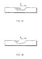
- FIGS. 1 a and 1 bare side diagrammatic views of a wafer indicating the angles resulting from etching, where the wall angle varies with the manner in which the wafer is etched.
- the angle formed between ⁇ 100> and ⁇ 111>is 54.74° as shown in FIG. 1 ( a ).
- FIG. 1 ( a )To make a 45° angle, the approach of using wafers that were cut 9.74° off the ⁇ 100> orientation was used. Such wafers were purchased from Virginia Semiconductors.
- FIG. 2shows the fabrication process.
- a 0.2-3 ⁇ m (2 ⁇ m; the actual exemplification will be indicated in parentheses) thick silicon dioxide layer 202(FIG. 2 ( a )) is thermally grown on both sides of a silicon wafer 201 .
- 0.1-4 ⁇ m (2 ⁇ m) thick Shipley S1818 photoresist 203is spin-coated on both sides of the wafer, as shown in FIG. 2 ( b ).
- the photoresist layer 203 on the wafer front sideis photolithographically patterned (FIG. 2 ( c )).
- the silicon dioxide layer 202then is etched (FIG.
- photoresist layer 203in a hydrofluoric acid solution buffered with ammonium fluoride, using photoresist layer 203 as the mask.
- the photoresist layer 203 at the back side of the waferprotects the silicon dioxide layer 202 from being etched.
- the wafer 201is left with the silicon dioxide layer 202 shown in FIG. 2 ( e ).
- 0.2-2 ⁇ m (0.5 ⁇ m) thick silicon nitride layer 204is deposited on both sides of the silicon wafer 201 using low pressure chemical vapor deposition (LPCVD).
- LPCVDlow pressure chemical vapor deposition
- Another layer of photoresist 205is spun on both sides of the wafer (FIG.
- FIG. 2 ( g )The silicon nitride layer 204 is etched using SF 6 /O 2 plasma etching process with photoresist layer 205 as the mask shown in FIG. 2 ( i ).
- FIG. 2 ( j )the underlying silicon dioxide layer 202 is etched in hydrofluoric acid solution buffered with ammonium fluoride.
- the photoresist layer 205is stripped (FIG. 2 ( k )).
- the wafer 201is then etched in 5-40% (20%) potassium hydroxide solution at 40-100° C. (60° C.) (FIG.
- the silicon nitride layer 204is etched using SF 6 /O 2 plasma etching without using a mask layer.
- the SF 6 /O 2 plasma etching processhas relatively high etching selectivity of silicon nitride 204 over silicon dioxide 202 and 206 . Because of this, the silicon nitride layer 204 is completely removed while the silicon dioxide layer 202 and 206 is not etched significantly.
- the silicon wafer 201is then etched (FIG. 2 ( o )) using a deep reactive ion etching (DRIE) process to form 50 ⁇ m deep channels with vertical sidewalls. Finally, the silicon dioxide layer 202 and 206 is stripped (FIG. 2 ( p )).
- DRIEdeep reactive ion etching
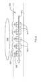
- FIG. 3is a diagrammatic view of a group of channels with two optical elements.
- the device 300has several light beams 301 from light sources (not shown).
- the light beams 301are conveniently a laser beam.
- the device 300has microfabricated capillary channels 302 and microfabricated optical channels 303 , having walls 304 , which are shown at a 45° angle.
- the microfabricated optic 303is a microfluidic channel, where reflection may be accomplished by coating the surface of the channel with a reflective layer, e.g. aluminum, or the channeled may be filled with air or other material of a different refractive index from the wall material, such that total internal reflection occurs when the laser beam strikes the wall 304 surface.
- the wall 304should be optically flat.
- the channel surfaces or walls 305should also be substantially optically flat and at a 90° angle to the planar surface of device 300 and, therefore, normal to the laser beam propagation 301 .
- fluorophores in the channels 302fluorescence emission is detected perpendicular to the device 300 by an optical system 306 .
- Any convenient optical detection systemmay be employed, e.g. a CCD, photocells, photodiode, photomultiplier tubes etc.
- the autofluorescence from the walls 307 separating the channels 302will provide a very small contribution to the fluorescence emitted from the channel 302 .
- the device 400comprises a plurality of sample channels 401 interspersed with sheath flow channels 402 .
- the sample channels 401have outlets 403 and the sheath flow channels 402 have outlets 404 for directing the flow of liquid into streambed 405 .
- the liquid in sample channels 401will be an aqueous electrically conductive liquid, having a component to be measured.
- the liquid carrierwill be an aqueous buffer.
- the sheath flow liquidmay be the same liquid as the carrier or a different liquid, having the same or different composition and viscosity. The rate of flow of the streams of sample liquid and sheath flow liquid will be adjusted to provide the desired width of the sample liquid in the detection region 406 and the desired spacing between sample streams.
- Optical elements 407 and 408are positioned on opposite sides of the detection region 406 , whereby light reflected from optical element 407 is propagated through the detection region 406 and the sample streams and reflected into a light dump by optical element 408 . Fluorescence emitted from detection region 406 is detected by an appropriate fluorimetric detection system, not shown.
- the devicemay be modified by having microlenses integrated into the top plate.
- the microfabricated devicemay have several inegrated microlenses 601 incorporated into the top plate to substantially capture more fluorescence 602 excited within the microfluidic channels 603 .
- the walls 604 of channels 602may or may not be substantially optically flat and may or may not be precisely at a 90° angle, usually deviating at most by about 10° from the planar surface of the device 600 .
- the light beam 605 used to excite the fluorescence within the microfluidic channelsmay propagated through the channels at an angle substantially parallel to the planar surface of the device or deviate from such angle, usually by not more than about 10°.
- further focussing of the light from the individual channels onto a detector array or fiber optic array leading to a detector arraymay be implemented by a focussing lens system 606 .
- FIG. 5is a diagrammatic plan view of the layout of the chip as employed in the subject invention and as depicted in cross-section in FIG. 3 .
- the microfluidic device 500has a plurality of capillary channels with differing lengths. Two of the microfluidic channels 504 and 506 have injection cross-channels 508 and 510 , respectively. Each of the channels has reservoirs 512 at opposite ends of the channel, in which electrodes, not shown, are placed. By appropriate activation of the electrodes, either electroosmotic flow or electrophoretic flow occurs in the channels 502 .
- Optical channels 514 and 516are placed on opposite sides of channels 502 , where laser light from a laser source, not shown, may be directed from the wall of optical channel 514 through the channels 512 and reflected to a waste dump by optical channel 516 .
- a fluorescent detectornot shown, detects fluorescence in the region of the light path between optical channels 514 and 516 .
- the two etching steps to create the V grooves and the vertical sidewall channelscan be swapped without changing any other processing steps. Also, other techniques such as aligning wafers to different orientations can be used to create the 45° angle channels.
- the chip designis as depicted in FIG. 5 , where the chip dimensions are 4 in square; the cast chips were enclosed with Mitsubishi films UN6.53.91 and UN6.53.92.
- the subject inventionprovides for an efficient method for irradiating fluorophores in microchannels or capillary channels, or it parallel streams lacking physical dividers.
- the irradiation lightcan be efficiently directed across a number of streams without causing significant autofluorescence and provides for sharp bands in the detection region.
- the devicescan be readily manufactured to provide the desired channels and then be used for performing a variety of operations in a channel where the outcome is a fluorescent signal.
Landscapes
- Chemical & Material Sciences (AREA)
- Health & Medical Sciences (AREA)
- Analytical Chemistry (AREA)
- General Health & Medical Sciences (AREA)
- Chemical Kinetics & Catalysis (AREA)
- Engineering & Computer Science (AREA)
- Hematology (AREA)
- Clinical Laboratory Science (AREA)
- Physics & Mathematics (AREA)
- Immunology (AREA)
- Optics & Photonics (AREA)
- Nuclear Medicine, Radiotherapy & Molecular Imaging (AREA)
- Life Sciences & Earth Sciences (AREA)
- Biochemistry (AREA)
- General Physics & Mathematics (AREA)
- Pathology (AREA)
- Dispersion Chemistry (AREA)
- Manufacturing & Machinery (AREA)
- Microelectronics & Electronic Packaging (AREA)
- Investigating, Analyzing Materials By Fluorescence Or Luminescence (AREA)
Abstract
Description
This application claims the benefit of the filing date of U.S. provisional application 60/153,644 filed Sep. 13, 1999, which disclosure is hereby incorporated by reference.
The field of this invention is irradiation and detection of light emitting entities in microchannels and the fabrication of devices for this purpose.
Microfluidics employs small capillary channels or microchannels in a solid substrate to perform a wide variety of operations. By employing electrical fields with conductive fluids in the microchannels, very small volumes may be accurately moved, reagents mixed, and the presence of an entity of interest determined. In many applications, the determination is fluorescence. Fluorescence can provide for high sensitivity, allows for multiplexing, by detecting photons at different wavelengths; by appropriate use of combinations of fluorophores one can employ a single light source for excitation. In addition, there are a large number of different commercially available detection devices. In addition, many assays have been developed which depend upon the use of fluorescence, such as DNA sequencing, receptor assays dependent upon expression of green fluorescent protein, immunoassays employing a fluorescent label, etc.
In the case of microfluidics, the use of plastics as the substrate has found application. While plastics have the advantage of ease of fabrication, cost and ready availability, they tend to be fluorescent. In addition, when irradiating a sample with excitation light, light scatter results in a significant background signal, particularly when the excitation pathway and emission pathway are the same. While some systems provide for an obtuse angle between the excitation and emission optical pathways, in the case of microfluidics there are the problems of directing the excitation light to the center of the microchannel, the small amount of sample that will be exposed to the irradiation and the substantially diminished fluorescent signal that one observes at an angle from the microchannel. Also, since the excitation light will encounter the device substrate, there is the further fluorescence of the substrate added to the fluorescent signal.
There is, therefore, an interest in designing new approaches to excitation of fluorophores in microchannels and detecting the fluorescent emission efficiently.
U.S. Patents of interest include U.S. Pat. No. 4,863,560, “Fabrication of Silicon Structures by Single Side, Multiple Step Etching Process”; U.S. Pat. No. 5,006,202, “Fabrication Method for Silicon Devices Using a Two Step Silicon Etching Process”; and U.S. Pat. No. 5,738,757, “Planar Masking for Multi-Depth Silicon Etching.” Publications of interest include Backlund and Rosengren, “New shapes in (100) Si using KOH and EDP etches,” J. Micromach. Microeng. 1992, 2:75-79; Sekimura and Naruse, Fabrication of 45° optical mirrors on (100) silicon using surfactant-added TMAH solution,” International Conference on Solid State Sensors and Actuators, pp. 550-551, Sendai, Japan, Jun. 7-10, 1999; Strandman, et al., “Fabrication of 45° Mirrors Together with Well-Defined V-grooves Using Wet Anisotropic Etching of Silicon, J. of Microelectromechanical Systems (MEMS) and Chang and Hicks, “Mesa structure formation using potassium hydroxide and ethylene diamine based etchants.” IEEE Workshop on Solid State Sensors and Actuators, pp. 102-103, Hilton Head, S.C., June 1988.
Methods and devices are provided for an optical system for emission detection from microchannels in plastic substrates. A master is formed for plastic molding of a microfluidic device, where the device has parallel fluid streams, optionally separated with at least substantially perpendicular side walls, and on each side of said streams is a microfabricated optic, having reflecting walls for directing a light beam through the streams and then into a waste light dump. The master is formed by separately etching different microstructures, with appropriate masking and different protective coatings, which are individually removed prior to final etching to provide deep microstructures. Microfabrication techniques are provided for molding microfluidic devices employing the optical system for use in fluorescent based operations.
The subject invention provides microfluidic devices comprising optical systems, methods of making the microfluidic devices and methods of using the microfluidic devices. The microfluidic devices comprise a fluid streambed with at least one stream, usually at least two streams. The individual streams may be divided by at least substantially 90° walls parallel to each other and desirably perpendicular to the base or floor of the microchannel, or individual streams separated by liquid separators, creating a plurality of microchannels having parallel regions. Disposed on each side of the fluid stream bed are optical elements comprising a first reflective wall for receiving a light beam and directing the light beam through the fluid stream bed and a second reflective wall for receiving the light beam from the fluid stream bed and directing the light beam to a light waste dump.
To produce the microfluidic devices, a positive form (same structure as the final product) is fabricated, which form is used to make a mold for molding microfluidic devices from plastics. The positive form is fabricated by initially providing differential protective coatings over sites of different microstructures using appropriate masking and protective coatings, followed by deep etching the different microstructures independently after differential removal of the protective coatings. The resulting devices may be used in microfluidic operations, where the fluid streambed of parallel streams is used to detect fluorescence from a fluorophore present in the streambed region. A light source directs light through the fluid streambed by means of the optical elements and the fluorescent light is detected normal to the direction of the light beam. In this way, the signal-to-noise ratio is greatly enhanced, interference from fluorescence of the substrate used to produce the device is minimized and simple optical excitation and emission detection systems may be employed.
In producing the microfluidic devices, a form is fabricated from which a mold can be produced. The form is conveniently made from a silicon wafer using microfabrication techniques. The subject method for preparing the form employs a planar masking process for etching deep silicon structures with different cross-sectional profiles that allows patterning of multiple structures before etching while the wafer surface is still planar. The process also provides protection for the previously etched structures during the later etching steps using selective thin-film deposition/growth and, therefore eliminates photoresist spin coating on deep etched structures. In carrying out the process, the channels are produced at one stage and the optical elements at another stage, by employing appropriate masking, protective coatings and etching.
The methodology uses semiconductor lithographic technology. The process involves forming and partially removing layers of silicon dioxide and silicon nitride, enlisting the use of photoresist layers as masks and etching portions of the underlying substrate and/or protective silicon oxide/nitride coatings unprotected by the photoresist. Chemical vapor deposition is employed for providing protective layers of silicon nitride, where layers of silicon oxide and silicon nitride may be differentially removed. The method is described in greater detail in reference toFIG. 2 , where the device has walls for separating the different streams in the fluid streambed.
The process is used to produce silicon chips having microstructures in said silicon chip of different cross-sections and depths of greater than about 5 μm, usually greater than about 10 μm and may be 100 μm or more, where depths of 5 μm create problems of having a uniform photoresist coated using spin coating. The method comprises the steps of: growing silicon dioxide on both sides of a silicon wafer; spin-coating both sides of said wafer with photoresist; photolithographically patterning a first side of said wafer to define sites for at least one of a first set of microstructures;
- etching said silicon dioxide layer at sites above areas to be etched to form at least one of a first set of microstructures; stripping said photoresist from said wafer; depositing a silicon nitride layer on both sides of said silicon wafer; spin-coating on both sides of said wafer with photoresist; photolithographically patterning said first side of said wafer to define sites for at least one of a second set of microstructures having a different cross-section from said first set of microstructures; etching said silicon nitride layer at sites above areas to be etched to form said second set of microstructures and silicon dioxide underneath said silicon nitride layer to expose said silicon wafer;
- etching said silicon wafer to form at least one of said second microstructures; coating exposed portions of said wafer with silicon dioxide; removing remaining portions of said silicon nitride layer and exposing said wafer at said sites of said at least one of a first set of microstructures; and etching said silicon wafer to form said first microstructures.
By using the process described above, one may prepare devices, where a plurality of liquid streams are irradiated orthogonally to their direction of flow. The device substrate will usually be of a thickness in the range of about 0.2 mm to 1 cm, more usually 1 mm to 5 mm. The substrate will usually be enclosed with a transparent plastic film of from about 5 to 100 μm thickness. The plurality of liquid streams may be separated by walls constructed in the device or by sheath flow, where the device provides a liquid stream to separate the liquid streams comprising the fluorophore to be measured. Each of the devices will have two optical elements on opposite sides of the liquid streams to be irradiated. Generally, the optical elements will be separated by at least about 0.1 mm, more usually at least about 1 mm, and not more than about 25 mm, usually not more than about 10 mm. The spacing between the optical elements will depend upon the number of liquid streams to be irradiated, whether the streams are separated by liquid or solid spacers, the width of the streams, the nature of the light source, the diffusion of the light beam, and the like. There will generally be at least 2 streams between optical elements, more usually at least about 3 streams, and not more than about 12 streams, usually not more than about 10 streams. By using a multiplicity of optical elements on each side of a group of streams, one can provide for as many streams as one wishes to have irradiated. Since each optical element may have two reflective sides, one side may be used for irradiation of the streams and the other side may be used to direct the light from a different optical element, which light has passed through the streams, to a waste light dump. In an alternative embodiment, the optical element for directing light to a waste light dump is not required where the light will be dispersed within the substrate of the device.
The optical element is a channel, which may or may not be the length of the liquid stream. The optical element will have a wall, which reflects the light beam. The depth and length of the optical element need only be sufficient to fulfill its function of directing a light beam. The length of the optical element will usually be at least about 1 mm and not more than the length of the stream. The depth will usually be at least about 10% of the depth of the streambed and up to and including the depth of the streambed, although it may be extended further, if desired. Reflection may be as a result of a difference in refractive index between the substrate and the contents of the optical element channel, a reflecting surface inside the channel, e.g. aluminum, silver, etc., or other means for light transfer. Where the optical element channel is between two groups of streams, it will have two reflecting walls, one normally for directing the light beam into the streams and the other for reflecting the light received from the streams into a light dump. While it is not necessary to have the walls at a 45° angle to the planar surface of the device, this angle is the most convenient, since the light source can be directed normal to the surface of the device and will be reflected at a 90° angle to the light beam from the light source. Otherwise, the light source will be placed at an angle to the optical element channel wall, which provides that the light be reflected in a line or plane parallel to the surface of the device. The angle of the wall will usually be in the range of about 45±15°.
When solid walls are present in the streambed, they will have a width of about 0.1 to 100 μm, more usually about 1 to 50 μm. The height of the wall will generally be about 2 to 500 μm, more usually about 5 to 100 μm, while the spacing between the walls forming the channels will usually be in the range of about 5 to 500 μm, more usually about 10 to 200 μm. When solid walls are not present in the streambed, namely the streams are separated by liquid walls or streams using sheath flow, separation between streams will be at least about 10 μm, more usually at least about 20 μm, and not more than about 100 μm, usually not more than about 50 μm.
The subject devices find particular use with multiplexed devices, which produce a plurality of streams having a fluorescent entity for detection. These devices are exemplified by electrokinetic devices, where the electrokinetic devices have a plurality of units, each unit producing an independent stream for analysis. The subject device may be part of an electrokinetic device, so as to be integrated with the substrate used for forming the electrokinetic units. The electrokinetic devices are characterized by having a channel, which will feed the stream into the detection device of the subject invention. In this instance, the walls of the electrokinetic device may have the same orientation as the walls of the electrokinetic device or the electrokinetic wall channels be tapered to join with the detection device walls.
In the situation with the liquid walls or streams, the streams from the electrokinetic units will generally be tapered down to reduce the length of the irradiation beam through the streams. The electrokinetic device capillary channels will generally have a width in the range of about 10 to 500 μm, where the walls or spacing between the channels will usually be in the range of about 10 to 1000μ, more usually in the range of about 100 to 500 μm. The tapering area will generally reduce the cross-section of the capillary channels and walls by at least about 30%, preferably at least about 50% and may result in a reduction of 75% or more. The tapering area will have angled sides, where the angle may vary in the range of about 5 to 65°, usually about 45°±15°. The distance between the outlets from the capillary channels and the detection region in the streambed will generally be at least about 0.1 mm, more usually at least about 1 mm and not more than about 10 mm, generally being from about 1 to 5 mm, being controlled by the angle of narrowing, the width of the detection region, the width of the channel area feeding the detection region, the depth of the stream bed and the volume of liquid exiting from the capillary channels into the streambed. The width of the detection region will be in the range of about 0.2 to 50 mm, more usually about 0.5 to 20 mm.
The irradiation region will normally be only a small portion of the stream bed channel, which stream bed channel may be straight or tortuous and of the same or different dimensions from the region of the channels in the irradiation region. Where the stream bed does not have dividing walls, the streams emanating from the capillary channels will generally have a stream width in the range of about 0.1 to 50μ, more usually about 1 to 20μ. There will be at least one stream between optical elements and not more than about 100, usually not more than about 50, generally in the range of about 5 to 50. As discussed previously, the number of streams will be controlled by the effectiveness of the radiation beam and its ability to remain sharp while passing through the streams to ensure a predetermined area of exposure of a desired level of intensity.
There may be one or a plurality of groups of streams bordered by optical elements. For a device, there will be at least one group and there may be two or more, where the groups may be in a single line or be distributed throughout a wafer having a plurality of capillary electrokinetic units. Each of the capillary electrokinetic units will usually have at least three reservoirs and two intersecting channels, where the intersections may be a cross-intersection or a T-intersection. Of course, the units may be much more sophisticated, where a greater number of chambers and channels may be involved, including mixing chambers, additional reservoirs, separation channels, injection channels, etc. Also, there will usually be at least three, usually at least four electrodes, where the electrodes are used to create electrical fields in the channels to move particles by electrokinesis, which includes electrophoresis and electroosmotic force or flow (“EOF”).
The subject devices may be prepared as follows. A silicon wafer cut about 9.74° off the <100> orientation is employed to form the (opposite configuration from the final product), which may then be used to produce a negative mold for forming the devices in plastic. The first step is growing a silicon dioxide layer on at least one surface of said silicon wafer. This is followed by photolithographically etching one side of said wafer to remove said silicon dioxide at predetermined sites for channel formation. The silicon wafer is then coated on at least the side in which the channels are to be formed with silicon nitride. To form an optical channel, the channel side is photolithographically etched to expose the silicon at an optical channel site, followed by etching the optical channel site with anisotropic silicon etchant, e.g. hydroxide (5 to 40%) at an elevated temperature (40 to 100° C.) to produce a V-shaped groove at a 45° angle. The exposed silicon in the optical channel is oxidized to silicon oxide, followed by removing remaining silicon nitride and etching the silicon wafer through said silicon dioxide layer to form channels with 90° separating walls. The resulting positive mold may then be used to produce a negative mold to be used for fabricating the subject devices. In an alternative approach, the wafer substrate may be aluminum or some other appropriate composition where microfeatures are cut into the substrate through diamond ruling or turning.
To demonstrate the subject invention a chip was prepared as follows:
InFIGS. 1 aand1bare side diagrammatic views of a wafer indicating the angles resulting from etching, where the wall angle varies with the manner in which the wafer is etched. In the common wet etching of <100> silicon wafers, the angle formed between <100> and <111> is 54.74° as shown in FIG.1(a). To make a 45° angle, the approach of using wafers that were cut 9.74° off the <100> orientation was used. Such wafers were purchased from Virginia Semiconductors.
InFIG. 3 is a diagrammatic view of a group of channels with two optical elements. Thedevice 300 has severallight beams 301 from light sources (not shown). The light beams301 are conveniently a laser beam. Thedevice 300 has microfabricatedcapillary channels 302 and microfabricatedoptical channels 303, havingwalls 304, which are shown at a 45° angle. Themicrofabricated optic 303 is a microfluidic channel, where reflection may be accomplished by coating the surface of the channel with a reflective layer, e.g. aluminum, or the channeled may be filled with air or other material of a different refractive index from the wall material, such that total internal reflection occurs when the laser beam strikes thewall 304 surface. Thewall 304 should be optically flat. The channel surfaces orwalls 305 should also be substantially optically flat and at a 90° angle to the planar surface ofdevice 300 and, therefore, normal to thelaser beam propagation 301. With fluorophores in thechannels 302, fluorescence emission is detected perpendicular to thedevice 300 by anoptical system 306. Any convenient optical detection system may be employed, e.g. a CCD, photocells, photodiode, photomultiplier tubes etc. The autofluorescence from thewalls 307 separating thechannels 302 will provide a very small contribution to the fluorescence emitted from thechannel 302.
InFIG. 4 , thedevice 400 comprises a plurality ofsample channels 401 interspersed withsheath flow channels 402. Thesample channels 401 haveoutlets 403 and thesheath flow channels 402 haveoutlets 404 for directing the flow of liquid intostreambed 405. For the most part, the liquid insample channels 401 will be an aqueous electrically conductive liquid, having a component to be measured. Frequently, the liquid carrier will be an aqueous buffer. The sheath flow liquid may be the same liquid as the carrier or a different liquid, having the same or different composition and viscosity. The rate of flow of the streams of sample liquid and sheath flow liquid will be adjusted to provide the desired width of the sample liquid in thedetection region 406 and the desired spacing between sample streams.Optical elements detection region 406, whereby light reflected fromoptical element 407 is propagated through thedetection region 406 and the sample streams and reflected into a light dump byoptical element 408. Fluorescence emitted fromdetection region 406 is detected by an appropriate fluorimetric detection system, not shown.
The device may be modified by having microlenses integrated into the top plate. As seen inFIG. 6 , the microfabricated device may have severalinegrated microlenses 601 incorporated into the top plate to substantially capturemore fluorescence 602 excited within themicrofluidic channels 603. Thewalls 604 ofchannels 602 may or may not be substantially optically flat and may or may not be precisely at a 90° angle, usually deviating at most by about 10° from the planar surface of thedevice 600. Thelight beam 605 used to excite the fluorescence within the microfluidic channels may propagated through the channels at an angle substantially parallel to the planar surface of the device or deviate from such angle, usually by not more than about 10°. In addition to themicrolenses 601, further focussing of the light from the individual channels onto a detector array or fiber optic array leading to a detector array may be implemented by a focussinglens system 606.
InFIG. 5 is a diagrammatic plan view of the layout of the chip as employed in the subject invention and as depicted in cross-section in FIG.3. Themicrofluidic device 500 has a plurality of capillary channels with differing lengths. Two of themicrofluidic channels reservoirs 512 at opposite ends of the channel, in which electrodes, not shown, are placed. By appropriate activation of the electrodes, either electroosmotic flow or electrophoretic flow occurs in thechannels 502.Optical channels 514 and516 are placed on opposite sides ofchannels 502, where laser light from a laser source, not shown, may be directed from the wall ofoptical channel 514 through thechannels 512 and reflected to a waste dump by optical channel516. A fluorescent detector, not shown, detects fluorescence in the region of the light path betweenoptical channels 514 and516.
In the above process, the two etching steps to create the V grooves and the vertical sidewall channels can be swapped without changing any other processing steps. Also, other techniques such as aligning wafers to different orientations can be used to create the 45° angle channels. The chip design is as depicted inFIG. 5 , where the chip dimensions are 4 in square; the cast chips were enclosed with Mitsubishi films UN6.53.91 and UN6.53.92.
To test the effectiveness of the devices for irradiation of fluorophores and reduction of autofluorescence of the chips, a video was taken of the events using a camera attached to an inverted epifluorescence microscope with 488 nm laser at 6 mW and viewing through an OG bandpass filter. A 100 μM TAMRA solution in TBE was employed and diluted in TBE to the final concentration. All images were viewed through a 10×10.45 objective, except the phase contrast image, which used a 20×10.45/Ph 1 objective.
Clear bands were observed with both 1 μM and 10 nM TAMRA. Little, if any, autofluorescence was observed. With dye in the channels, a sharp band of fluorescence is observed at the sight where the light beam passes through the TAMRA containing solution, with the fluorescence intensity related to the concentration of the fluorophore. Above the chip, a scatter pattern is observed, probably resulting from multiple reflections in the chip.
It is evident from the above results that the subject invention provides for an efficient method for irradiating fluorophores in microchannels or capillary channels, or it parallel streams lacking physical dividers. The irradiation light can be efficiently directed across a number of streams without causing significant autofluorescence and provides for sharp bands in the detection region. The devices can be readily manufactured to provide the desired channels and then be used for performing a variety of operations in a channel where the outcome is a fluorescent signal.
Although the foregoing invention has been described in some detail by way of illustration and example for purposes of clarity of understanding, it will be readily apparent to those of ordinary skill in the art in light of the teachings of this invention that certain changes and modifications may be made thereto without departing from the spirit or scope of the appended claims.
Claims (17)
1. An irradiation device for irradiating a plurality of streams of capillary dimensions, said device comprising:
a substrate comprising a streambed for receiving a plurality of liquid streams of capillary dimensions;
capillaries in liquid transferring relationship with said streambed for forming said streams;
optical channels on opposite sides of said stream bed having reflecting walls confronting said streambed and parallel to the direction of said streams, one of said reflecting walls positioned for receiving light from light source and directing said light orthogonally through said streambed, and the other of said optical channels for reflecting said light to a light dump.
2. An irradiation device according toclaim 1 , further comprising a laser light source positioned at an angle to said reflecting wall to direct light orthogonally from said reflecting wall.
3. An irradiation device according toclaim 2 , wherein said reflecting walls are at 45° to the base of said device.
4. An irradiation device according toclaim 1 , wherein said reflecting walls are at 45° to the base of said device.
5. An irradiation device according toclaim 1 , wherein said streambed further comprises separating walls for physically separating said streams in said streambed, said separating walls at a 90° to said streambed.
6. An irradiation device according toclaim 1 , further comprising sheath flow capillaries interspersed between said stream capillaries to provide liquid separation between said streams.
7. An irradiation device for irradiating a plurality of streams of capillary dimensions, said device comprising:
a substrate comprising a streambed for receiving a plurality of liquid streams of capillary dimensions, said streambed divided into a plurality of capillary-sized zones by perpendicular walls;
capillaries in liquid transferring relationship with said streambed for forming and directing individual streams into said zones;
electrokinetic means for moving said streams from said capillaries into said streambed; and
optical channels on opposite sides of said stream bed having reflecting walls confronting said streambed and parallel to the direction of said streams, one of said reflecting walls positioned for receiving light from light source and directing said light orthogonally through said streambed, and the other of said optical channels for reflecting said light to a light dump.
8. An irradiation device according toclaim 7 , wherein said reflecting walls are coated with a reflecting coating.
9. An irradiation device according toclaim 7 , wherein said optical channels are filled with air.
10. An irradiation device according toclaim 7 , wherein said substrate is plastic and said stream bed is enclosed.
11. An irradiation device for irradiating a plurality of streams of capillary dimensions, said device comprising:
a substrate comprising a streambed for receiving a plurality of liquid streams of capillary dimensions;
a cover enclosing said streambed;
capillaries in liquid transferring relationship with said streambed for forming said streams;
electrokinetic means for moving said streams from said capillaries into said streambed;
sheath flow capillaries interspersed between said capillaries;
a reservoir in fluid transfer relationship with said sheath flow capillaries; and
optical channels on opposite sides of said stream bed having reflecting walls confronting said streambed and parallel to the direction of said streams, one of said reflecting walls positioned for receiving light from light source and directing said light orthogonally through said streambed, and the other of said optical charnels for reflecting said light to a light dump.
12. An irradiation device according toclaim 11 , wherein said reflecting walls are have a reflecting coating.
13. An irradiation device according toclaim 11 , wherein said optical channels are filled with air.
14. An irradiation device for irradiating a stream of capillary dimensions, said device comprising:
a substrate comprising a streambed for receiving a liquid stream of capillary dimensions;
one or more capillaries in liquid transferring relationship with said streambed for forming said stream;
an optical channel on one side of said stream bed having reflecting walls confronting said streambed and parallel to the direction of said stream, one of said reflecting walls positioned for receiving light from light source and directing said light orthogonally through said streambed.
15. An irradiation device according toclaim 14 further comprising an optical channel on the other side of said stream bed having reflecting walls confronting said streambed and parallel to the direction of said stream, one of said reflecting walls positioned for reflecting light from said streambed to a light dump.
16. An irradiation device according toclaim 14 wherein said substrate comprises a streambed for receiving a plurality of liquid streams of capillary dimensions for irradiation.
17. An irradiation device according toclaim 15 wherein said substrate comprises a streambed for receiving a plurality of liquid streams of capillary dimensions for irradiation.
Priority Applications (1)
| Application Number | Priority Date | Filing Date | Title |
|---|---|---|---|
| US09/660,992US6906797B1 (en) | 1999-09-13 | 2000-09-13 | Side light activated microfluid channels |
Applications Claiming Priority (2)
| Application Number | Priority Date | Filing Date | Title |
|---|---|---|---|
| US15364499P | 1999-09-13 | 1999-09-13 | |
| US09/660,992US6906797B1 (en) | 1999-09-13 | 2000-09-13 | Side light activated microfluid channels |
Publications (1)
| Publication Number | Publication Date |
|---|---|
| US6906797B1true US6906797B1 (en) | 2005-06-14 |
Family
ID=34635992
Family Applications (1)
| Application Number | Title | Priority Date | Filing Date |
|---|---|---|---|
| US09/660,992Expired - LifetimeUS6906797B1 (en) | 1999-09-13 | 2000-09-13 | Side light activated microfluid channels |
Country Status (1)
| Country | Link |
|---|---|
| US (1) | US6906797B1 (en) |
Cited By (54)
| Publication number | Priority date | Publication date | Assignee | Title |
|---|---|---|---|---|
| US20040053404A1 (en)* | 2001-08-24 | 2004-03-18 | Grossman Paul D. | Separation device substrate including non-fluorescent quencher dye |
| US20050000812A1 (en)* | 2001-07-25 | 2005-01-06 | Francois Couderc | Apparatus for electrophoresis separation on microchannels and for laser-induced fluorescence detection |
| US20050030541A1 (en)* | 2003-06-30 | 2005-02-10 | Andreas Erlbacher | Device and method for analyzing samples |
| WO2007074038A1 (en)* | 2005-12-23 | 2007-07-05 | INSTITUT FüR MIKROTECHNIK MAINZ GMBH | Measurement chip |
| US20070206186A1 (en)* | 2006-03-06 | 2007-09-06 | Manish Sharma | Capillary based optical measurement system |
| US20090051901A1 (en)* | 2007-08-24 | 2009-02-26 | Pao-Lin Shen | Integrated microfluidic optical device for sub-micro liter liquid sample microspectroscopy |
| WO2009029177A1 (en)* | 2007-08-24 | 2009-03-05 | Dynamic Throughput Inc. | Integrated microfluidic optical device for sub-micro liter liquid sample microspectroscopy |
| US20090097022A1 (en)* | 2007-08-24 | 2009-04-16 | Dynamic Throughput Inc. | Discovery tool with integrated microfluidic biomarker optical detection array device and methods for use |
| US20100158756A1 (en)* | 2008-12-18 | 2010-06-24 | Claros Diagnostics, Inc. | Reagent storage in microfluidic systems and related articles and methods |
| US20100196207A1 (en)* | 2009-02-02 | 2010-08-05 | David Steinmiller | Structures for controlling light interaction with microfluidic devices |
| CN102023146A (en)* | 2010-09-28 | 2011-04-20 | 上海理工大学 | Electrophoretic chip for optical detection and electrophoretic device thereof |
| US8133671B2 (en) | 2007-07-13 | 2012-03-13 | Handylab, Inc. | Integrated apparatus for performing nucleic acid extraction and diagnostic testing on multiple biological samples |
| US8182763B2 (en) | 2007-07-13 | 2012-05-22 | Handylab, Inc. | Rack for sample tubes and reagent holders |
| US8216530B2 (en) | 2007-07-13 | 2012-07-10 | Handylab, Inc. | Reagent tube |
| USD665095S1 (en) | 2008-07-11 | 2012-08-07 | Handylab, Inc. | Reagent holder |
| US8273308B2 (en) | 2001-03-28 | 2012-09-25 | Handylab, Inc. | Moving microdroplets in a microfluidic device |
| US8287820B2 (en) | 2007-07-13 | 2012-10-16 | Handylab, Inc. | Automated pipetting apparatus having a combined liquid pump and pipette head system |
| USD669191S1 (en) | 2008-07-14 | 2012-10-16 | Handylab, Inc. | Microfluidic cartridge |
| US8323900B2 (en) | 2006-03-24 | 2012-12-04 | Handylab, Inc. | Microfluidic system for amplifying and detecting polynucleotides in parallel |
| US8323584B2 (en) | 2001-09-12 | 2012-12-04 | Handylab, Inc. | Method of controlling a microfluidic device having a reduced number of input and output connections |
| US8324372B2 (en) | 2007-07-13 | 2012-12-04 | Handylab, Inc. | Polynucleotide capture materials, and methods of using same |
| US8415103B2 (en) | 2007-07-13 | 2013-04-09 | Handylab, Inc. | Microfluidic cartridge |
| US8420015B2 (en) | 2001-03-28 | 2013-04-16 | Handylab, Inc. | Systems and methods for thermal actuation of microfluidic devices |
| US8440149B2 (en) | 2001-02-14 | 2013-05-14 | Handylab, Inc. | Heat-reduction methods and systems related to microfluidic devices |
| US8473104B2 (en) | 2001-03-28 | 2013-06-25 | Handylab, Inc. | Methods and systems for control of microfluidic devices |
| US8470586B2 (en) | 2004-05-03 | 2013-06-25 | Handylab, Inc. | Processing polynucleotide-containing samples |
| WO2013114333A1 (en)* | 2012-02-04 | 2013-08-08 | Centre For Cellular And Molecular Platforms (C-Camp) | Microfluidic flow analyzer for pathological detection and method thereof |
| USD692162S1 (en) | 2011-09-30 | 2013-10-22 | Becton, Dickinson And Company | Single piece reagent holder |
| US8617905B2 (en) | 1995-09-15 | 2013-12-31 | The Regents Of The University Of Michigan | Thermal microvalves |
| US8665071B2 (en) | 2004-03-19 | 2014-03-04 | Applied Biosystems, Llc | Methods and systems for using RFID in biological field |
| US8679831B2 (en) | 2003-07-31 | 2014-03-25 | Handylab, Inc. | Processing particle-containing samples |
| US8709787B2 (en) | 2006-11-14 | 2014-04-29 | Handylab, Inc. | Microfluidic cartridge and method of using same |
| US8765062B2 (en) | 2010-04-16 | 2014-07-01 | Opko Diagnostics, Llc | Systems and devices for analysis of samples |
| US8802445B2 (en) | 2007-05-04 | 2014-08-12 | Opko Diagnostics, Llc | Fluidic connectors and microfluidic systems |
| JP2014153265A (en)* | 2013-02-12 | 2014-08-25 | Shinko Electric Ind Co Ltd | Micro flow passage, manufacturing method thereof, and optical analyzer |
| US8852862B2 (en) | 2004-05-03 | 2014-10-07 | Handylab, Inc. | Method for processing polynucleotide-containing samples |
| US8883490B2 (en) | 2006-03-24 | 2014-11-11 | Handylab, Inc. | Fluorescence detector for microfluidic diagnostic system |
| US8895311B1 (en) | 2001-03-28 | 2014-11-25 | Handylab, Inc. | Methods and systems for control of general purpose microfluidic devices |
| US20150118738A1 (en)* | 2009-05-14 | 2015-04-30 | Canon U.S. Life Sciences, Inc. | Microfluidic chip features for optical and thermal isolation |
| US9040288B2 (en) | 2006-03-24 | 2015-05-26 | Handylab, Inc. | Integrated system for processing microfluidic samples, and method of using the same |
| US9075051B2 (en) | 2009-11-24 | 2015-07-07 | Opko Diagnostics, Llc | Fluid mixing and delivery in microfluidic systems |
| US9186677B2 (en) | 2007-07-13 | 2015-11-17 | Handylab, Inc. | Integrated apparatus for performing nucleic acid extraction and diagnostic testing on multiple biological samples |
| US9222954B2 (en) | 2011-09-30 | 2015-12-29 | Becton, Dickinson And Company | Unitized reagent strip |
| US9618139B2 (en) | 2007-07-13 | 2017-04-11 | Handylab, Inc. | Integrated heater and magnetic separator |
| USD787087S1 (en) | 2008-07-14 | 2017-05-16 | Handylab, Inc. | Housing |
| US9765389B2 (en) | 2011-04-15 | 2017-09-19 | Becton, Dickinson And Company | Scanning real-time microfluidic thermocycler and methods for synchronized thermocycling and scanning optical detection |
| US10672503B2 (en) | 2012-03-05 | 2020-06-02 | Opko Diagnostics, Llc | Methods and apparatuses for conducting analyses |
| US10822644B2 (en) | 2012-02-03 | 2020-11-03 | Becton, Dickinson And Company | External files for distribution of molecular diagnostic tests and determination of compatibility between tests |
| US10900066B2 (en) | 2006-03-24 | 2021-01-26 | Handylab, Inc. | Microfluidic system for amplifying and detecting polynucleotides in parallel |
| US11002752B2 (en) | 2009-09-21 | 2021-05-11 | Pocared Diagnostics Ltd. | System for conducting the identification of bacteria in biological samples |
| US11112416B2 (en) | 2018-01-30 | 2021-09-07 | Life Technologies Corporation | Instruments, devices and consumables for use in a workflow of a smart molecular analysis system |
| EP2245467B1 (en)* | 2008-02-05 | 2022-04-06 | Pocared Diagnostics Ltd. | System for conducting the identification of bacteria in biological samples |
| US11453906B2 (en) | 2011-11-04 | 2022-09-27 | Handylab, Inc. | Multiplexed diagnostic detection apparatus and methods |
| US11806718B2 (en) | 2006-03-24 | 2023-11-07 | Handylab, Inc. | Fluorescence detector for microfluidic diagnostic system |
Citations (14)
| Publication number | Priority date | Publication date | Assignee | Title |
|---|---|---|---|---|
| US4863560A (en) | 1988-08-22 | 1989-09-05 | Xerox Corp | Fabrication of silicon structures by single side, multiple step etching process |
| US5006202A (en) | 1990-06-04 | 1991-04-09 | Xerox Corporation | Fabricating method for silicon devices using a two step silicon etching process |
| US5637458A (en)* | 1994-07-20 | 1997-06-10 | Sios, Inc. | Apparatus and method for the detection and assay of organic molecules |
| US5738757A (en) | 1995-11-22 | 1998-04-14 | Northrop Grumman Corporation | Planar masking for multi-depth silicon etching |
| US5741411A (en)* | 1995-05-19 | 1998-04-21 | Iowa State University Research Foundation | Multiplexed capillary electrophoresis system |
| US5846708A (en)* | 1991-11-19 | 1998-12-08 | Massachusetts Institiute Of Technology | Optical and electrical methods and apparatus for molecule detection |
| US5858187A (en)* | 1996-09-26 | 1999-01-12 | Lockheed Martin Energy Systems, Inc. | Apparatus and method for performing electrodynamic focusing on a microchip |
| US5948227A (en)* | 1997-12-17 | 1999-09-07 | Caliper Technologies Corp. | Methods and systems for performing electrophoretic molecular separations |
| US5948684A (en)* | 1997-03-31 | 1999-09-07 | University Of Washington | Simultaneous analyte determination and reference balancing in reference T-sensor devices |
| US6156273A (en)* | 1997-05-27 | 2000-12-05 | Purdue Research Corporation | Separation columns and methods for manufacturing the improved separation columns |
| US6558945B1 (en)* | 1999-03-08 | 2003-05-06 | Aclara Biosciences, Inc. | Method and device for rapid color detection |
| US6660149B1 (en)* | 1997-10-24 | 2003-12-09 | Beckman Coulter, Inc. | Multichannel microscale system for high throughput preparative separation with comprehensive collection and analysis |
| US6676819B1 (en)* | 1999-09-14 | 2004-01-13 | Yaoqing Diana Liu | Methods and apparatus for automatic on-line multi-dimensional electrophoresis |
| US6759662B1 (en)* | 1998-07-28 | 2004-07-06 | Ce Resources Pte. Ltd. | Optical detection system |
- 2000
- 2000-09-13USUS09/660,992patent/US6906797B1/ennot_activeExpired - Lifetime
Patent Citations (14)
| Publication number | Priority date | Publication date | Assignee | Title |
|---|---|---|---|---|
| US4863560A (en) | 1988-08-22 | 1989-09-05 | Xerox Corp | Fabrication of silicon structures by single side, multiple step etching process |
| US5006202A (en) | 1990-06-04 | 1991-04-09 | Xerox Corporation | Fabricating method for silicon devices using a two step silicon etching process |
| US5846708A (en)* | 1991-11-19 | 1998-12-08 | Massachusetts Institiute Of Technology | Optical and electrical methods and apparatus for molecule detection |
| US5637458A (en)* | 1994-07-20 | 1997-06-10 | Sios, Inc. | Apparatus and method for the detection and assay of organic molecules |
| US5741411A (en)* | 1995-05-19 | 1998-04-21 | Iowa State University Research Foundation | Multiplexed capillary electrophoresis system |
| US5738757A (en) | 1995-11-22 | 1998-04-14 | Northrop Grumman Corporation | Planar masking for multi-depth silicon etching |
| US5858187A (en)* | 1996-09-26 | 1999-01-12 | Lockheed Martin Energy Systems, Inc. | Apparatus and method for performing electrodynamic focusing on a microchip |
| US5948684A (en)* | 1997-03-31 | 1999-09-07 | University Of Washington | Simultaneous analyte determination and reference balancing in reference T-sensor devices |
| US6156273A (en)* | 1997-05-27 | 2000-12-05 | Purdue Research Corporation | Separation columns and methods for manufacturing the improved separation columns |
| US6660149B1 (en)* | 1997-10-24 | 2003-12-09 | Beckman Coulter, Inc. | Multichannel microscale system for high throughput preparative separation with comprehensive collection and analysis |
| US5948227A (en)* | 1997-12-17 | 1999-09-07 | Caliper Technologies Corp. | Methods and systems for performing electrophoretic molecular separations |
| US6759662B1 (en)* | 1998-07-28 | 2004-07-06 | Ce Resources Pte. Ltd. | Optical detection system |
| US6558945B1 (en)* | 1999-03-08 | 2003-05-06 | Aclara Biosciences, Inc. | Method and device for rapid color detection |
| US6676819B1 (en)* | 1999-09-14 | 2004-01-13 | Yaoqing Diana Liu | Methods and apparatus for automatic on-line multi-dimensional electrophoresis |
Non-Patent Citations (4)
| Title |
|---|
| Backlund et al., "New shapes in (100) Si using KOH and EDP etches", J. Micromech. Microeng. 2:75-79,1992. |
| Chang et al., "Mesa Structure Formation Using Potassium Hydroxide and Ethylene Diamine Based Etchants", IEEE Workshop on Solid State Sensors and Actuators, pp. 102-103, Hilton Head, SC, Jun. 1988. |
| Sekimura et al., "Fabrication of 45° Optical Mirrors on (100) Silicon Using Surfactant-Added TMAH Solution", International Conference on Solid State Sensors and Actuators, pp. 550-551, Jun. 7-10, 1999. |
| Strandman et al., "Fabrication of 45° optical mirrors on (100) Si using wet anisotropic etching", Proceedings of the Workshop on Micro Electrical Mechanical Systems (MEMS), vol. Workshop 8, pp. 244-249, Jan. 29, 1995. |
Cited By (172)
| Publication number | Priority date | Publication date | Assignee | Title |
|---|---|---|---|---|
| US8617905B2 (en) | 1995-09-15 | 2013-12-31 | The Regents Of The University Of Michigan | Thermal microvalves |
| US9528142B2 (en) | 2001-02-14 | 2016-12-27 | Handylab, Inc. | Heat-reduction methods and systems related to microfluidic devices |
| US8734733B2 (en) | 2001-02-14 | 2014-05-27 | Handylab, Inc. | Heat-reduction methods and systems related to microfluidic devices |
| US8440149B2 (en) | 2001-02-14 | 2013-05-14 | Handylab, Inc. | Heat-reduction methods and systems related to microfluidic devices |
| US9051604B2 (en) | 2001-02-14 | 2015-06-09 | Handylab, Inc. | Heat-reduction methods and systems related to microfluidic devices |
| US8895311B1 (en) | 2001-03-28 | 2014-11-25 | Handylab, Inc. | Methods and systems for control of general purpose microfluidic devices |
| US8768517B2 (en) | 2001-03-28 | 2014-07-01 | Handylab, Inc. | Methods and systems for control of microfluidic devices |
| US9677121B2 (en) | 2001-03-28 | 2017-06-13 | Handylab, Inc. | Systems and methods for thermal actuation of microfluidic devices |
| US8420015B2 (en) | 2001-03-28 | 2013-04-16 | Handylab, Inc. | Systems and methods for thermal actuation of microfluidic devices |
| US10351901B2 (en) | 2001-03-28 | 2019-07-16 | Handylab, Inc. | Systems and methods for thermal actuation of microfluidic devices |
| US8473104B2 (en) | 2001-03-28 | 2013-06-25 | Handylab, Inc. | Methods and systems for control of microfluidic devices |
| US9259735B2 (en) | 2001-03-28 | 2016-02-16 | Handylab, Inc. | Methods and systems for control of microfluidic devices |
| US10571935B2 (en) | 2001-03-28 | 2020-02-25 | Handylab, Inc. | Methods and systems for control of general purpose microfluidic devices |
| US8894947B2 (en) | 2001-03-28 | 2014-11-25 | Handylab, Inc. | Systems and methods for thermal actuation of microfluidic devices |
| US8703069B2 (en) | 2001-03-28 | 2014-04-22 | Handylab, Inc. | Moving microdroplets in a microfluidic device |
| US10619191B2 (en) | 2001-03-28 | 2020-04-14 | Handylab, Inc. | Systems and methods for thermal actuation of microfluidic devices |
| US8273308B2 (en) | 2001-03-28 | 2012-09-25 | Handylab, Inc. | Moving microdroplets in a microfluidic device |
| US20050000812A1 (en)* | 2001-07-25 | 2005-01-06 | Francois Couderc | Apparatus for electrophoresis separation on microchannels and for laser-induced fluorescence detection |
| US20040053404A1 (en)* | 2001-08-24 | 2004-03-18 | Grossman Paul D. | Separation device substrate including non-fluorescent quencher dye |
| US7019831B2 (en)* | 2001-08-24 | 2006-03-28 | Applera Corporation | Separation device substrate including non-fluorescent quencher dye |
| US8323584B2 (en) | 2001-09-12 | 2012-12-04 | Handylab, Inc. | Method of controlling a microfluidic device having a reduced number of input and output connections |
| US8685341B2 (en) | 2001-09-12 | 2014-04-01 | Handylab, Inc. | Microfluidic devices having a reduced number of input and output connections |
| US9028773B2 (en) | 2001-09-12 | 2015-05-12 | Handylab, Inc. | Microfluidic devices having a reduced number of input and output connections |
| US20050030541A1 (en)* | 2003-06-30 | 2005-02-10 | Andreas Erlbacher | Device and method for analyzing samples |
| US7202945B2 (en)* | 2003-06-30 | 2007-04-10 | Tecan Trading Ag | Device and method for analyzing samples |
| US8679831B2 (en) | 2003-07-31 | 2014-03-25 | Handylab, Inc. | Processing particle-containing samples |
| US11078523B2 (en) | 2003-07-31 | 2021-08-03 | Handylab, Inc. | Processing particle-containing samples |
| US9670528B2 (en) | 2003-07-31 | 2017-06-06 | Handylab, Inc. | Processing particle-containing samples |
| US10731201B2 (en) | 2003-07-31 | 2020-08-04 | Handylab, Inc. | Processing particle-containing samples |
| US10865437B2 (en) | 2003-07-31 | 2020-12-15 | Handylab, Inc. | Processing particle-containing samples |
| US12139745B2 (en) | 2003-07-31 | 2024-11-12 | Handylab, Inc. | Processing particle-containing samples |
| US8665071B2 (en) | 2004-03-19 | 2014-03-04 | Applied Biosystems, Llc | Methods and systems for using RFID in biological field |
| US8669849B2 (en) | 2004-03-19 | 2014-03-11 | Applied Biosystems, Llc | Methods and systems for using RFID in biological field |
| US9530035B2 (en) | 2004-03-19 | 2016-12-27 | Applied Biosystems, Llc | Methods and systems for using RFID in biological field |
| US10369573B2 (en) | 2004-03-19 | 2019-08-06 | Applied Biosystems, Llc | Methods and systems for using RFID in biological field |
| US9019079B2 (en) | 2004-03-19 | 2015-04-28 | Applied Biosystems, Llc | Methods and systems for using RFID in biological field |
| US8669848B2 (en) | 2004-03-19 | 2014-03-11 | Applied Biosystems, Llc | Methods and systems for using RFID in biological field |
| US10443088B1 (en) | 2004-05-03 | 2019-10-15 | Handylab, Inc. | Method for processing polynucleotide-containing samples |
| US8470586B2 (en) | 2004-05-03 | 2013-06-25 | Handylab, Inc. | Processing polynucleotide-containing samples |
| US10364456B2 (en) | 2004-05-03 | 2019-07-30 | Handylab, Inc. | Method for processing polynucleotide-containing samples |
| US10494663B1 (en) | 2004-05-03 | 2019-12-03 | Handylab, Inc. | Method for processing polynucleotide-containing samples |
| US11441171B2 (en) | 2004-05-03 | 2022-09-13 | Handylab, Inc. | Method for processing polynucleotide-containing samples |
| US10604788B2 (en) | 2004-05-03 | 2020-03-31 | Handylab, Inc. | System for processing polynucleotide-containing samples |
| US8852862B2 (en) | 2004-05-03 | 2014-10-07 | Handylab, Inc. | Method for processing polynucleotide-containing samples |
| US7894071B2 (en)* | 2005-12-23 | 2011-02-22 | Institut Fuer Mikrotechnik Mainz Gmbh | Measurement chip |
| WO2007074038A1 (en)* | 2005-12-23 | 2007-07-05 | INSTITUT FüR MIKROTECHNIK MAINZ GMBH | Measurement chip |
| US20090161108A1 (en)* | 2005-12-23 | 2009-06-25 | Institut Fuer Mikrotechnik Mainz Gmbh | Measurement Chip |
| DE102005062174C5 (en)* | 2005-12-23 | 2010-05-06 | INSTITUT FüR MIKROTECHNIK MAINZ GMBH | measuring chip |
| US20070206186A1 (en)* | 2006-03-06 | 2007-09-06 | Manish Sharma | Capillary based optical measurement system |
| US7515261B2 (en)* | 2006-03-06 | 2009-04-07 | Hewlett-Packard Development Company, L.P. | Capillary based optical measurement system |
| US8883490B2 (en) | 2006-03-24 | 2014-11-11 | Handylab, Inc. | Fluorescence detector for microfluidic diagnostic system |
| US9040288B2 (en) | 2006-03-24 | 2015-05-26 | Handylab, Inc. | Integrated system for processing microfluidic samples, and method of using the same |
| US10695764B2 (en) | 2006-03-24 | 2020-06-30 | Handylab, Inc. | Fluorescence detector for microfluidic diagnostic system |
| US11806718B2 (en) | 2006-03-24 | 2023-11-07 | Handylab, Inc. | Fluorescence detector for microfluidic diagnostic system |
| US11666903B2 (en) | 2006-03-24 | 2023-06-06 | Handylab, Inc. | Integrated system for processing microfluidic samples, and method of using same |
| US10900066B2 (en) | 2006-03-24 | 2021-01-26 | Handylab, Inc. | Microfluidic system for amplifying and detecting polynucleotides in parallel |
| US8323900B2 (en) | 2006-03-24 | 2012-12-04 | Handylab, Inc. | Microfluidic system for amplifying and detecting polynucleotides in parallel |
| US11959126B2 (en) | 2006-03-24 | 2024-04-16 | Handylab, Inc. | Microfluidic system for amplifying and detecting polynucleotides in parallel |
| US10799862B2 (en) | 2006-03-24 | 2020-10-13 | Handylab, Inc. | Integrated system for processing microfluidic samples, and method of using same |
| US11141734B2 (en) | 2006-03-24 | 2021-10-12 | Handylab, Inc. | Fluorescence detector for microfluidic diagnostic system |
| US10821446B1 (en) | 2006-03-24 | 2020-11-03 | Handylab, Inc. | Fluorescence detector for microfluidic diagnostic system |
| US10821436B2 (en) | 2006-03-24 | 2020-11-03 | Handylab, Inc. | Integrated system for processing microfluidic samples, and method of using the same |
| US11142785B2 (en) | 2006-03-24 | 2021-10-12 | Handylab, Inc. | Microfluidic system for amplifying and detecting polynucleotides in parallel |
| US12162007B2 (en) | 2006-03-24 | 2024-12-10 | Handylab, Inc. | Integrated system for processing microfluidic samples, and method of using same |
| US9802199B2 (en) | 2006-03-24 | 2017-10-31 | Handylab, Inc. | Fluorescence detector for microfluidic diagnostic system |
| US10857535B2 (en) | 2006-03-24 | 2020-12-08 | Handylab, Inc. | Integrated system for processing microfluidic samples, and method of using same |
| US10843188B2 (en) | 2006-03-24 | 2020-11-24 | Handylab, Inc. | Integrated system for processing microfluidic samples, and method of using the same |
| US9080207B2 (en) | 2006-03-24 | 2015-07-14 | Handylab, Inc. | Microfluidic system for amplifying and detecting polynucleotides in parallel |
| US11085069B2 (en) | 2006-03-24 | 2021-08-10 | Handylab, Inc. | Microfluidic system for amplifying and detecting polynucleotides in parallel |
| US10913061B2 (en) | 2006-03-24 | 2021-02-09 | Handylab, Inc. | Integrated system for processing microfluidic samples, and method of using the same |
| US9815057B2 (en) | 2006-11-14 | 2017-11-14 | Handylab, Inc. | Microfluidic cartridge and method of making same |
| US12128405B2 (en) | 2006-11-14 | 2024-10-29 | Handylab, Inc. | Microfluidic valve and method of making same |
| US10710069B2 (en) | 2006-11-14 | 2020-07-14 | Handylab, Inc. | Microfluidic valve and method of making same |
| US8709787B2 (en) | 2006-11-14 | 2014-04-29 | Handylab, Inc. | Microfluidic cartridge and method of using same |
| US12030050B2 (en) | 2006-11-14 | 2024-07-09 | Handylab, Inc. | Microfluidic cartridge and method of making same |
| US8765076B2 (en) | 2006-11-14 | 2014-07-01 | Handylab, Inc. | Microfluidic valve and method of making same |
| US10775369B2 (en) | 2007-05-04 | 2020-09-15 | Opko Diagnostics, Llc | Fluidic systems for analyses |
| US9234888B2 (en) | 2007-05-04 | 2016-01-12 | Opko Diagnostics, Llc | Fluidic connectors and microfluidic systems |
| US8802445B2 (en) | 2007-05-04 | 2014-08-12 | Opko Diagnostics, Llc | Fluidic connectors and microfluidic systems |
| US10408824B2 (en) | 2007-05-04 | 2019-09-10 | Opko Diagnostics, Llc | Fluidic connectors and microfluidic systems |
| US9075047B2 (en) | 2007-05-04 | 2015-07-07 | Opko Diagnostics, Llc | Fluidic connectors and microfluidic systems |
| US8324372B2 (en) | 2007-07-13 | 2012-12-04 | Handylab, Inc. | Polynucleotide capture materials, and methods of using same |
| US9186677B2 (en) | 2007-07-13 | 2015-11-17 | Handylab, Inc. | Integrated apparatus for performing nucleic acid extraction and diagnostic testing on multiple biological samples |
| US10625261B2 (en) | 2007-07-13 | 2020-04-21 | Handylab, Inc. | Integrated apparatus for performing nucleic acid extraction and diagnostic testing on multiple biological samples |
| US9618139B2 (en) | 2007-07-13 | 2017-04-11 | Handylab, Inc. | Integrated heater and magnetic separator |
| US12128402B2 (en) | 2007-07-13 | 2024-10-29 | Handylab, Inc. | Microfluidic cartridge |
| US10632466B1 (en) | 2007-07-13 | 2020-04-28 | Handylab, Inc. | Integrated apparatus for performing nucleic acid extraction and diagnostic testing on multiple biological samples |
| US11845081B2 (en) | 2007-07-13 | 2023-12-19 | Handylab, Inc. | Integrated apparatus for performing nucleic acid extraction and diagnostic testing on multiple biological samples |
| US10590410B2 (en) | 2007-07-13 | 2020-03-17 | Handylab, Inc. | Polynucleotide capture materials, and methods of using same |
| US11549959B2 (en) | 2007-07-13 | 2023-01-10 | Handylab, Inc. | Automated pipetting apparatus having a combined liquid pump and pipette head system |
| US9701957B2 (en) | 2007-07-13 | 2017-07-11 | Handylab, Inc. | Reagent holder, and kits containing same |
| US11466263B2 (en) | 2007-07-13 | 2022-10-11 | Handylab, Inc. | Diagnostic apparatus to extract nucleic acids including a magnetic assembly and a heater assembly |
| US8133671B2 (en) | 2007-07-13 | 2012-03-13 | Handylab, Inc. | Integrated apparatus for performing nucleic acid extraction and diagnostic testing on multiple biological samples |
| US12397295B2 (en) | 2007-07-13 | 2025-08-26 | Handylab, Inc. | Integrated apparatus for performing nucleic acid extraction and diagnostic testing on multiple biological samples |
| US9217143B2 (en) | 2007-07-13 | 2015-12-22 | Handylab, Inc. | Polynucleotide capture materials, and methods of using same |
| US9259734B2 (en) | 2007-07-13 | 2016-02-16 | Handylab, Inc. | Integrated apparatus for performing nucleic acid extraction and diagnostic testing on multiple biological samples |
| US11266987B2 (en) | 2007-07-13 | 2022-03-08 | Handylab, Inc. | Microfluidic cartridge |
| US11254927B2 (en) | 2007-07-13 | 2022-02-22 | Handylab, Inc. | Polynucleotide capture materials, and systems using same |
| US8182763B2 (en) | 2007-07-13 | 2012-05-22 | Handylab, Inc. | Rack for sample tubes and reagent holders |
| US9238223B2 (en) | 2007-07-13 | 2016-01-19 | Handylab, Inc. | Microfluidic cartridge |
| US8216530B2 (en) | 2007-07-13 | 2012-07-10 | Handylab, Inc. | Reagent tube |
| US10139012B2 (en) | 2007-07-13 | 2018-11-27 | Handylab, Inc. | Integrated heater and magnetic separator |
| US10071376B2 (en) | 2007-07-13 | 2018-09-11 | Handylab, Inc. | Integrated apparatus for performing nucleic acid extraction and diagnostic testing on multiple biological samples |
| US11060082B2 (en) | 2007-07-13 | 2021-07-13 | Handy Lab, Inc. | Polynucleotide capture materials, and systems using same |
| US10100302B2 (en) | 2007-07-13 | 2018-10-16 | Handylab, Inc. | Polynucleotide capture materials, and methods of using same |
| US8287820B2 (en) | 2007-07-13 | 2012-10-16 | Handylab, Inc. | Automated pipetting apparatus having a combined liquid pump and pipette head system |
| US10065185B2 (en) | 2007-07-13 | 2018-09-04 | Handylab, Inc. | Microfluidic cartridge |
| US10179910B2 (en) | 2007-07-13 | 2019-01-15 | Handylab, Inc. | Rack for sample tubes and reagent holders |
| US10234474B2 (en) | 2007-07-13 | 2019-03-19 | Handylab, Inc. | Automated pipetting apparatus having a combined liquid pump and pipette head system |
| US10875022B2 (en) | 2007-07-13 | 2020-12-29 | Handylab, Inc. | Integrated apparatus for performing nucleic acid extraction and diagnostic testing on multiple biological samples |
| US10625262B2 (en) | 2007-07-13 | 2020-04-21 | Handylab, Inc. | Integrated apparatus for performing nucleic acid extraction and diagnostic testing on multiple biological samples |
| US10717085B2 (en) | 2007-07-13 | 2020-07-21 | Handylab, Inc. | Integrated apparatus for performing nucleic acid extraction and diagnostic testing on multiple biological samples |
| US9347586B2 (en) | 2007-07-13 | 2016-05-24 | Handylab, Inc. | Automated pipetting apparatus having a combined liquid pump and pipette head system |
| US8415103B2 (en) | 2007-07-13 | 2013-04-09 | Handylab, Inc. | Microfluidic cartridge |
| US10844368B2 (en) | 2007-07-13 | 2020-11-24 | Handylab, Inc. | Diagnostic apparatus to extract nucleic acids including a magnetic assembly and a heater assembly |
| US8710211B2 (en) | 2007-07-13 | 2014-04-29 | Handylab, Inc. | Polynucleotide capture materials, and methods of using same |
| US20090051901A1 (en)* | 2007-08-24 | 2009-02-26 | Pao-Lin Shen | Integrated microfluidic optical device for sub-micro liter liquid sample microspectroscopy |
| US7952705B2 (en) | 2007-08-24 | 2011-05-31 | Dynamic Throughput Inc. | Integrated microfluidic optical device for sub-micro liter liquid sample microspectroscopy |
| US20090097022A1 (en)* | 2007-08-24 | 2009-04-16 | Dynamic Throughput Inc. | Discovery tool with integrated microfluidic biomarker optical detection array device and methods for use |
| WO2009029177A1 (en)* | 2007-08-24 | 2009-03-05 | Dynamic Throughput Inc. | Integrated microfluidic optical device for sub-micro liter liquid sample microspectroscopy |
| EP2245467B1 (en)* | 2008-02-05 | 2022-04-06 | Pocared Diagnostics Ltd. | System for conducting the identification of bacteria in biological samples |
| USD665095S1 (en) | 2008-07-11 | 2012-08-07 | Handylab, Inc. | Reagent holder |
| USD787087S1 (en) | 2008-07-14 | 2017-05-16 | Handylab, Inc. | Housing |
| USD669191S1 (en) | 2008-07-14 | 2012-10-16 | Handylab, Inc. | Microfluidic cartridge |
| US8591829B2 (en)* | 2008-12-18 | 2013-11-26 | Opko Diagnostics, Llc | Reagent storage in microfluidic systems and related articles and methods |
| US9561506B2 (en) | 2008-12-18 | 2017-02-07 | Opko Diagnostics, Llc | Reagent storage in microfluidic systems and related articles and methods |
| US9878324B2 (en) | 2008-12-18 | 2018-01-30 | Opko Diagnostics, Llc | Reagent storage in microfluidic systems and related articles and methods |
| US20100158756A1 (en)* | 2008-12-18 | 2010-06-24 | Claros Diagnostics, Inc. | Reagent storage in microfluidic systems and related articles and methods |
| US10589265B2 (en) | 2008-12-18 | 2020-03-17 | Opko Diagnostics, Llc | Reagent storage in microfluidic systems and related articles and methods |
| US9770715B2 (en) | 2009-02-02 | 2017-09-26 | Opko Diagnostics, Llc | Structures for controlling light interaction with microfluidic devices |
| US20100196207A1 (en)* | 2009-02-02 | 2010-08-05 | David Steinmiller | Structures for controlling light interaction with microfluidic devices |
| US9827564B2 (en) | 2009-02-02 | 2017-11-28 | Opko Diagnostics, Llc | Fluidic systems and methods for analyses |
| US9827563B2 (en) | 2009-02-02 | 2017-11-28 | Opko Diagnostics, Llc | Fluidic systems and methods for analyses |
| US8480975B2 (en) | 2009-02-02 | 2013-07-09 | Opko Diagnostics, Llc | Structures for controlling light interaction with microfluidic devices |
| US8802029B2 (en) | 2009-02-02 | 2014-08-12 | Opko Diagnostics, Llc | Structures for controlling light interaction with microfluidic devices |
| US8221700B2 (en) | 2009-02-02 | 2012-07-17 | Opko Diagnostics, Llc | Structures for controlling light interaction with microfluidic devices |
| US9234236B2 (en)* | 2009-05-14 | 2016-01-12 | Canon U.S. Life Sciences, Inc. | Microfluidic chip features for optical and thermal isolation |
| US20150118738A1 (en)* | 2009-05-14 | 2015-04-30 | Canon U.S. Life Sciences, Inc. | Microfluidic chip features for optical and thermal isolation |
| US11002752B2 (en) | 2009-09-21 | 2021-05-11 | Pocared Diagnostics Ltd. | System for conducting the identification of bacteria in biological samples |
| US9731291B2 (en) | 2009-11-24 | 2017-08-15 | Opko Diagnostics, Llc | Fluid mixing and delivery in microfluidic systems |
| US9075051B2 (en) | 2009-11-24 | 2015-07-07 | Opko Diagnostics, Llc | Fluid mixing and delivery in microfluidic systems |
| US10413899B2 (en) | 2009-11-24 | 2019-09-17 | Opko Diagnostics, Llc | Fluid mixing and delivery in microfluidic systems |
| US9682376B2 (en) | 2010-04-16 | 2017-06-20 | Opko Diagnostics, Llc | Systems and devices for analysis of samples |
| US9643182B2 (en) | 2010-04-16 | 2017-05-09 | Opko Diagnostics, Llc | Systems and devices for analysis of samples |
| US8932523B2 (en) | 2010-04-16 | 2015-01-13 | Opko Diagnostics, Llc | Systems and devices for analysis of samples |
| US9981266B2 (en) | 2010-04-16 | 2018-05-29 | Opko Diagnostics, Llc | Feedback control in microfluidic systems |
| US9116124B2 (en) | 2010-04-16 | 2015-08-25 | Opko Diagnostics, Llc | Feedback control in microfluidic systems |
| US8765062B2 (en) | 2010-04-16 | 2014-07-01 | Opko Diagnostics, Llc | Systems and devices for analysis of samples |
| US10456784B2 (en) | 2010-04-16 | 2019-10-29 | Opko Diagnostics, Llc | Systems and devices for analysis of samples |
| US11458473B2 (en) | 2010-04-16 | 2022-10-04 | Opko Diagnostics, Llc | Systems and devices for analysis of samples |
| CN102023146A (en)* | 2010-09-28 | 2011-04-20 | 上海理工大学 | Electrophoretic chip for optical detection and electrophoretic device thereof |
| US9765389B2 (en) | 2011-04-15 | 2017-09-19 | Becton, Dickinson And Company | Scanning real-time microfluidic thermocycler and methods for synchronized thermocycling and scanning optical detection |
| US11788127B2 (en) | 2011-04-15 | 2023-10-17 | Becton, Dickinson And Company | Scanning real-time microfluidic thermocycler and methods for synchronized thermocycling and scanning optical detection |
| US10781482B2 (en) | 2011-04-15 | 2020-09-22 | Becton, Dickinson And Company | Scanning real-time microfluidic thermocycler and methods for synchronized thermocycling and scanning optical detection |
| USD905269S1 (en) | 2011-09-30 | 2020-12-15 | Becton, Dickinson And Company | Single piece reagent holder |
| USD742027S1 (en) | 2011-09-30 | 2015-10-27 | Becton, Dickinson And Company | Single piece reagent holder |
| USD692162S1 (en) | 2011-09-30 | 2013-10-22 | Becton, Dickinson And Company | Single piece reagent holder |
| US9480983B2 (en) | 2011-09-30 | 2016-11-01 | Becton, Dickinson And Company | Unitized reagent strip |
| US10076754B2 (en) | 2011-09-30 | 2018-09-18 | Becton, Dickinson And Company | Unitized reagent strip |
| US9222954B2 (en) | 2011-09-30 | 2015-12-29 | Becton, Dickinson And Company | Unitized reagent strip |
| USD1029291S1 (en) | 2011-09-30 | 2024-05-28 | Becton, Dickinson And Company | Single piece reagent holder |
| USD831843S1 (en) | 2011-09-30 | 2018-10-23 | Becton, Dickinson And Company | Single piece reagent holder |
| US11453906B2 (en) | 2011-11-04 | 2022-09-27 | Handylab, Inc. | Multiplexed diagnostic detection apparatus and methods |
| US10822644B2 (en) | 2012-02-03 | 2020-11-03 | Becton, Dickinson And Company | External files for distribution of molecular diagnostic tests and determination of compatibility between tests |
| EA029557B1 (en)* | 2012-02-04 | 2018-04-30 | Сентр Фор Сельюлар Энд Молекьюлар Плэтформз (С-Кэмп) | Microfluidic flow analyzer for pathological detection and method thereof |
| WO2013114333A1 (en)* | 2012-02-04 | 2013-08-08 | Centre For Cellular And Molecular Platforms (C-Camp) | Microfluidic flow analyzer for pathological detection and method thereof |
| CN104136922A (en)* | 2012-02-04 | 2014-11-05 | 细胞和分子平台中心(C-Camp) | A microfluidic analyzer and method thereof |
| US9304122B2 (en) | 2012-02-04 | 2016-04-05 | Centre For Cellular And Molecular Platforms (C-Camp) | Microfluidic-based flow analyzer |
| US10672503B2 (en) | 2012-03-05 | 2020-06-02 | Opko Diagnostics, Llc | Methods and apparatuses for conducting analyses |
| JP2014153265A (en)* | 2013-02-12 | 2014-08-25 | Shinko Electric Ind Co Ltd | Micro flow passage, manufacturing method thereof, and optical analyzer |
| US11112416B2 (en) | 2018-01-30 | 2021-09-07 | Life Technologies Corporation | Instruments, devices and consumables for use in a workflow of a smart molecular analysis system |
| US12411148B2 (en) | 2018-01-30 | 2025-09-09 | Life Technologies Corporation | Instruments, devices and consumables for use in a workflow of a smart molecular analysis system |
Similar Documents
| Publication | Publication Date | Title |
|---|---|---|
| US6906797B1 (en) | Side light activated microfluid channels | |
| US12071340B2 (en) | Integrated analysis devices and related fabrication methods and analysis techniques | |
| US6815360B1 (en) | Silicon micro-machined projection with duct | |
| US6753200B2 (en) | Monolithic nanofluid sieving structures for DNA manipulation | |
| US6100541A (en) | Microfluidic devices and systems incorporating integrated optical elements | |
| US7087444B2 (en) | Method for integration of microelectronic components with microfluidic devices | |
| US8270781B2 (en) | Apparatus and method for improved optical detection of particles in fluid | |
| US20070102362A1 (en) | Chip | |
| EP3516369B1 (en) | Particle detection using thin lenses | |
| US20060073599A1 (en) | Microfabricated diffusion-based chemical sensor | |
| US20250237811A1 (en) | Optofluidic devices | |
| WO2001020309A1 (en) | Side light activated microfluid channels | |
| US20040251171A1 (en) | Separation apparatus, method of separation, and process for producing separation apparatus | |
| JP2023522692A (en) | Waveguide structure with aperture array | |
| US20020048809A1 (en) | Capillary array-based sample screening | |
| AU2015205826B2 (en) | Integrated nanofluidic analysis devices, fabrication methods and analysis techniques | |
| CN117642514A (en) | Array of integrated analytical devices with reduced scale cell wells |
Legal Events
| Date | Code | Title | Description |
|---|---|---|---|
| AS | Assignment | Owner name:ACLARA BIOSCIENCES, INC., CALIFORNIA Free format text:ASSIGNMENT OF ASSIGNORS INTEREST;ASSIGNORS:KAO, HUNG PIN;YANG, XING;REEL/FRAME:011206/0938;SIGNING DATES FROM 20001009 TO 20001013 | |
| STCF | Information on status: patent grant | Free format text:PATENTED CASE | |
| FPAY | Fee payment | Year of fee payment:4 | |
| AS | Assignment | Owner name:VIROLOGIC, INC., CALIFORNIA Free format text:MERGER;ASSIGNOR:APOLLO MERGER SUBSIDIARY, LLC;REEL/FRAME:028270/0008 Effective date:20050321 Owner name:MONOGRAM BIOSCIENCES, INC., CALIFORNIA Free format text:MERGER;ASSIGNOR:VIROLOGIC, INC.;REEL/FRAME:028270/0113 Effective date:20050906 Owner name:APOLLO MERGER SUBSIDIARY, LLC, CALIFORNIA Free format text:MERGER;ASSIGNOR:ACLARA BIOSCIENCES, INC.;REEL/FRAME:028269/0898 Effective date:20041210 | |
| FPAY | Fee payment | Year of fee payment:8 | |
| FPAY | Fee payment | Year of fee payment:12 |