US6906499B2 - Current mode bang-bang controller in a switching voltage regulator - Google Patents
Current mode bang-bang controller in a switching voltage regulatorDownload PDFInfo
- Publication number
- US6906499B2 US6906499B2US10/715,092US71509203AUS6906499B2US 6906499 B2US6906499 B2US 6906499B2US 71509203 AUS71509203 AUS 71509203AUS 6906499 B2US6906499 B2US 6906499B2
- Authority
- US
- United States
- Prior art keywords
- output
- regulator
- power driver
- voltage
- comparator
- Prior art date
- Legal status (The legal status is an assumption and is not a legal conclusion. Google has not performed a legal analysis and makes no representation as to the accuracy of the status listed.)
- Expired - Lifetime, expires
Links
Images


Classifications
- H—ELECTRICITY
- H02—GENERATION; CONVERSION OR DISTRIBUTION OF ELECTRIC POWER
- H02M—APPARATUS FOR CONVERSION BETWEEN AC AND AC, BETWEEN AC AND DC, OR BETWEEN DC AND DC, AND FOR USE WITH MAINS OR SIMILAR POWER SUPPLY SYSTEMS; CONVERSION OF DC OR AC INPUT POWER INTO SURGE OUTPUT POWER; CONTROL OR REGULATION THEREOF
- H02M3/00—Conversion of DC power input into DC power output
- H02M3/02—Conversion of DC power input into DC power output without intermediate conversion into AC
- H02M3/04—Conversion of DC power input into DC power output without intermediate conversion into AC by static converters
- H02M3/10—Conversion of DC power input into DC power output without intermediate conversion into AC by static converters using discharge tubes with control electrode or semiconductor devices with control electrode
- H02M3/145—Conversion of DC power input into DC power output without intermediate conversion into AC by static converters using discharge tubes with control electrode or semiconductor devices with control electrode using devices of a triode or transistor type requiring continuous application of a control signal
- H02M3/155—Conversion of DC power input into DC power output without intermediate conversion into AC by static converters using discharge tubes with control electrode or semiconductor devices with control electrode using devices of a triode or transistor type requiring continuous application of a control signal using semiconductor devices only
- H02M3/156—Conversion of DC power input into DC power output without intermediate conversion into AC by static converters using discharge tubes with control electrode or semiconductor devices with control electrode using devices of a triode or transistor type requiring continuous application of a control signal using semiconductor devices only with automatic control of output voltage or current, e.g. switching regulators
- H02M3/1563—Conversion of DC power input into DC power output without intermediate conversion into AC by static converters using discharge tubes with control electrode or semiconductor devices with control electrode using devices of a triode or transistor type requiring continuous application of a control signal using semiconductor devices only with automatic control of output voltage or current, e.g. switching regulators without using an external clock
Definitions
- the present inventionrelates generally to switching voltage regulators and in particular controllers in switching voltage regulators.
- Switching voltage regulatorsprovide regulated power supply voltages with high energy efficiency. These switching voltage regulators, however, either tend to respond poorly to rapid changes in load current or tend to have large steady state ripple. During transient intervals while the switching regulator is adjusting for the load, there tends to be undesirable amounts of overshoot and ripple in the output voltage.
- Embodiments of the present inventionprovide solutions to these and other problems, and offer other advantages over the prior art.
- the regulatorincludes a power driver having a feedback input and a power driver voltage.
- the regulatorincludes a comparator having a comparator output related to a combination of the load voltage and a power driver current.
- the regulatorincludes a pulse generator controlled by the comparator output and having output pulses with fixed pulse widths.
- the regulatorincludes a time limit circuit controlled by the output pulses. The time limit circuit provides the output pulses to the feedback input subject to a time limit between the output pulses.
- FIG. 1illustrates an oblique view of a disc drive.
- FIG. 2illustrates a power driver output waveform
- FIG. 3illustrates a first embodiment of a regulator.
- FIG. 4illustrates a second embodiment of a regulator.
- FIG. 5illustrates a third embodiment of a regulator with variable OFF time and an OFF time limit.
- FIG. 6illustrates a fourth embodiment of the a regulator with variable ON time and an ON time limit.
- FIG. 7illustrates a simulation timing diagram for the regulator illustrated in FIG. 5 .
- FIG. 8illustrates a first zoomed portion of the simulation timing diagram illustrated in FIG. 7 .
- FIG. 9illustrates a second zoomed portion of the simulation timing diagram illustrated in FIG. 7 .
- FIG. 10illustrates a third zoomed portion of the simulation timing diagram illustrated in FIG. 7 .
- FIGS. 11A , 11 Bschematically illustrate timing diagrams that show synchronization of various signals in FIGS. 5 , 6 .
- FIG. 12schematically illustrates an embodiment of a reference controlled by a current limit circuit to provide a soft start.
- a regulatorincludes a controller circuit that senses a combination of a load voltage and a power driver current of a power driver.
- the controller circuitprovides a controller output that is fed back to a feedback input of the power driver in order to control the load voltage.
- the controller outputcontrols a driver output to have a duty cycle that changes to adjust for load changes.
- an off time between fixed width ON pulsesis variable, but is also limited to a minimum value in order to minimize switching noise.
- an ON time between fixed width OFF timesis variable, but limited to a minimum value in order to minimize switching noise. The time limits avoid a problem with extremely short time pulses that can result in high frequency noise.
- the controller circuitcan be realized as a compact, low cost integrated circuit that is predominantly digital with a minimal amount of integrated analog circuits.
- the controllercan have the capability of fast response; minimum ripple on the regulated output voltage; low component count, stable control without the use of linear feedback, and small controller die size.
- the duty cycle and frequencyare constant during steady state, and variable during transient load. This constant duty cycle and frequency during steady state load condition results in lower noise in the system.
- the fixed minimum time featurereduces high frequency noise.
- the regulatoris especially useful in disc drive applications as described below in connection with FIG. 1 , but can also be used in many other voltage regulator applications.
- FIG. 1illustrates an oblique view of a disc drive 100 in which embodiments of the present invention are useful.
- Disc drive 100includes a housing with a base 102 and a top cover (not shown).
- Disc drive 100further includes a disc pack 106 , which is mounted on a spindle motor (not shown) by a disc clamp 108 .
- Disc pack 106includes a plurality of individual discs, which are mounted for co-rotation in a direction indicated by arrow 107 about central axis 109 .
- Each disc surfacehas an associated disc read/write head slider 110 which is mounted to disc drive 100 for communication with the disc surface.
- FIG. 1illustrates an oblique view of a disc drive 100 in which embodiments of the present invention are useful.
- Disc drive 100includes a housing with a base 102 and a top cover (not shown).
- Disc drive 100further includes a disc pack 106 , which is mounted on a spindle motor (not shown) by a disc
- sliders 110are supported by suspensions 112 which are in turn attached to track accessing arms 114 of an actuator 116 .
- the actuator shown in FIG. 1is of the type known as a rotary moving coil actuator and includes a voice coil motor (VCM), shown generally at 118 .
- VCMvoice coil motor
- Voice coil motor 118rotates actuator 116 with its attached read/write heads 110 about a pivot shaft 120 to position read/write heads 110 over a desired data track along an arcuate path 122 between a disc inner diameter 124 and a disc outer diameter 126 .
- Voice coil motor 118is driven by electronics 130 based on signals generated by read/write heads 110 and a host computer (not shown).
- Various functional blocks of electronics 130 and associated transducers in the disc drive 100can be energized by voltages that are regulated by voltage regulators such as those described below in connection with FIGS. 3-10 .
- FIG. 2illustrates an idealized power driver output waveform in a switching regulator.
- a vertical axis 140represents power driver output voltage and a horizontal axis 142 represents time.
- the power driverincludes switches that alternately connects the driver output to voltage VDD at 144 or voltage VSS at 146 , with transitional or switching intervals separating the conduction times of the switches to ensure that both switches are not conducting at the same time.
- the driver outputalternates between ON pulses 150 , 152 , 154 and OFF pulses 156 , 158 as illustrated.
- the ON pulse 150has an on time TON.
- the OFF time interval 156has an OFF time TOFF.
- a complete cycle of the power driver outputcan be seen as running from a start of ON pulse 150 to a start of ON PULSE 152 .
- the complete cyclehas a time duration TON+TOFF.
- a frequency of the power driver outputis defined as 1/(TON+TOFF) as illustrated in FIG. 2 .
- Voltage mode regulatorshave a frequency at the power driver output that can be either constant or variable.
- the voltage mode regulatorshave a slow response and relatively large ripple during transient load conditions, but have relatively low steady state ripple.
- the voltage mode regulatorsare relatively large and costly.
- Current mode regulatorshave a frequency at the power driver output that can be either constant or variable.
- the current mode regulatorshave slow response and relatively large ripple during transient load conditions, but have a relatively low steady state ripple.
- the current mode switching regulatorsare relatively large and costly.
- Hysteretic mode regulatorshave a frequency at the power driver output that is either variable or unpredictable.
- the hysteretic mode regulatorshave a fast response and relatively small ripple during transient load conditions, but have a relatively large steady state ripple.
- the hysteretic mode regulatorsare relatively low cost and small in size.
- the regulators described below in connection with FIGS. 3-10do not have any of the disadvantages described above of the voltage mode, current mode and hysteretic mode regulators.
- the regulators described below in connection with FIGS. 3-10do not regulate based solely on load voltage, but instead regulate based on a combination of the load voltage and the current provided by the power driver output.
- the regulators described belowhave power drive outputs that alternates between a pulse of one polarity with a fixed pulse width, and a pulse of the opposite polarity that has a variable pulse width that is limited to minimum pulse width.
- CMBBcurrent mode bang-bang regulators
- CMBB regulatorsprovide desirable regulator characteristics such as fast response and low ripple during transient load conditions, and low ripple during steady state conditions.
- the CMBB regulatorshave a variable but predictable frequency.
- the CMBB regulators described belowcombine desirable characteristics in a single design.
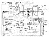
- FIG. 3illustrates a first embodiment of a regulator 201 that includes a controller circuit 200 .
- the controller circuit 200couples a controller output 202 to a feedback input 204 of a power driver 206 .
- the power driver 206provides a power driver output 208 .
- the power driver output 208couples a power driver current I (at 210 ) to a load 212 , and maintains a load voltage VOUT at 232 .
- the power driver 206serves to energize the electrical load 212 with a relatively constant voltage.
- the power driver current Ipasses through an impedance Z (at 295 ) that is connected to load voltage output VOUT at 232 .
- the arrangement of the impedance Z connected to VOUTgenerates a voltage on line 293 that is a combination of the load voltage VOUT and the power driver current I that is approximately VOUT+ZI.
- the impedance Zserves as a weighting factor so that the voltage on line 293 is a weighted sum of the load voltage and the power driver current.
- the controller output 202has a duty cycle that varies as a function of a voltage that the controller circuit 200 senses on line 293 .
- the controller circuit 200provides closed loop control of the power driver output 208 .
- the duty cycle at controller output 202is constant when the output current 210 is a fixed current.
- the duty cycleis variable when the output current 210 is a variable current.
- the electrical load 212is constant, the average output current 210 is a fixed current, the duty cycle is constant and the constant duty cycle tends to ensure a reduced level of noise at the power driver output 208 .
- the controller circuit 200comprises a comparator circuit 214 that couples to and senses the voltage on line 293 , which voltage is a combination of the load voltage at 232 and the power driver current I.
- the comparator circuit 214provides a comparator output 216 that indicates whether the voltage on line 293 is above or below a desired voltage level.
- the controller circuit 200also comprises a pulse generator 220 coupled to the comparator output 216 .
- the comparator output 216controls or triggers the pulse generator 220 .
- the pulse generator 220provides output pulses 221 at a pulse output 222 .
- the pulse output 222provides the output pulses 221 with a fixed time (pulse width) when the comparator circuit 214 indicates that the voltage sensed on line 293 is equal to the desired voltage level.
- the fixed pulse widthenergizes the output voltage back up again in the fixed on time case (see FIG. 11 A), but it discharges the output voltage during the fixed off time case (see FIG. 11 B).
- the fixed pulse widthcan be either an ON pulse width ( FIGS. 4-5 ) or, alternatively, an OFF pulse width (FIG. 6 ).
- the controller circuit 200also comprises a time limit circuit 225 coupled to the pulse output 222 .
- the pulses 221 at output 222control or trigger the time limit circuit 225 .
- the time limit circuit 225provides the controller output 202 that couples to the feedback input 204 .
- the time limit circuit 225passes on or replicates some of the pulses at the pulse output 222 .
- the time limit circuit 225generally passes on most of the pulses at the pulse output 222 . However, when pulses at the pulse output 222 are so closely spaced that the time of the variable portion of pulse output 222 becomes too short, then the time limit circuit 225 blanks, or does not pass on some of closely spaced fixed width pulses to the controller output 202 .
- This arrangementlimits a variable time of a pulse from the controller output 202 to an minimum time value.
- the time limit circuit 225limits an OFF time to a minimum off time value as described in more detail below in connection with FIGS. 4-5 .
- the time limit circuit 225limits an ON time to a minimum on time value as described in more detail below in connection with FIG. 6 .
- the minimum time valuelimits a frequency of a noise at the power driver output 208 to a maximum frequency. This arrangement reduces high frequency noise in the power driver current 210 associated with short spikes with widths shorter than the minimum time value. The quality of energization delivered to the electrical load 212 is improved.
- the time limit circuit 225can comprise an OFF time limit circuit 226 , and as described below in connection with FIG. 6 , the time limit circuit 225 can alternatively comprise an ON time limit circuit 227 .
- the controller circuit 200preferably also comprises a low pass filter 230 coupled to the power driver output 208 .
- the low pass filter 230provides a filtered regulator output 232 (load voltage) to the electrical load 212 .
- the use of the low pass filter 230further reduces high frequency noise that reaches the electrical load 212 .
- FIG. 4illustrates a second embodiment of a regulator 239 that includes a controller circuit 240 .
- Reference numbers used in FIG. 4 that are the same as reference numbers used in FIG. 3identify the same or similar features.
- An off time limit circuit 226comprises a first one shot circuit 242 and an AND gate 244 .
- a first input of the AND gate 244is coupled to an output 246 of the first one shot circuit 242 .
- the pulse output 222couples to a second input of the AND gate 244 and to an input of the first one shot circuit 242 .
- the first one shot 242has a one shot pulse width that sets an off time limit.
- the one shot output 246goes to a low level and provides blanking so that subsequent pulses from the pulse output 222 that are too closely spaced are blanked at the AND gate 244 and do not pass through to the output of the AND gate 244 .
- the pulse generator 220comprises a second one shot circuit 250 and an OR gate 252 .
- One input of the OR gate 252is coupled to an output 254 of the second one shot circuit 250 .
- the arrangementprovides a pulse output 222 that has pulses that are triggered by rising edges of pulses from the comparator output 216 , but are stretched in length by a pulse width of the second one shot 250 .
- the pulse width of the second one shot 250is a fixed pulse width.
- the OR gate 252provides an OR function.
- NOR gatesalso provide an OR function, and it will be understood by those skilled in the art that a NOR gate can be used in place of OR gate 252 if corresponding polarity inversions are made at inputs connected to the NOR gate output.
- the controller 240further comprises a reference circuit 260 that is included in the comparator circuit 214 .
- the comparator circuit 216also comprises a comparator 262 and a resistive voltage divider 264 that couples to the comparator 262 and a voltage VOUT+IR on line 293 .
- an impedance that carries the power driver current 210comprises a resistance R at 297 .
- the comparator 262provides a pulse on the comparator output 216 .
- the proportionis set by a resistance ratio in the resistive voltage divider 264 .
- the use of the voltage divider 264allows for use of a reference 260 that is conveniently within the range of power supply voltage rails.
- controller circuit 240 illustrated in FIG. 4is similar to the controller circuit 200 illustrated in FIG. 3 .
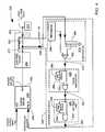
- FIG. 5illustrates a third embodiment of a regulator 279 that includes a controller circuit 280 with variable OFF time and an OFF time limit.
- Reference numbers used in FIG. 5 that are the same as reference numbers used in FIG. 4identify the same or similar features.
- the controller circuit 280is preferably formed as an integrated circuit 282 indicated by a dotted line surrounding portions of circuitry that are included in the integrated circuit. Other functional blocks (not illustrated) can also be included in the integrated circuit 282 .
- the integrated circuit 282can also include synchronous driver logic 284 and drivers 286 , 288 that are part of the power driver 206 .
- the components of integrated circuit 282are preferably all produced on a single silicon chip for low cost production.
- the integrated circuit 282can be a predominantly digital integrated circuit, limiting the use of complex linear amplifier circuitry that uses large areas of silicon real estate.
- the regulator 279comprises a current mode bang-bang switching regulator and the control output 202 has a duty cycle that controls the power driver 206 .
- the current mode bang-bang switching regulatorpreferably includes MOSFETs 290 , 292 .
- the transistor 290is turned on to connect a positive (VDD) rail to the power driver output 208 .
- the transistor 292is turned on to connect DC common (VSS) to the power driver output 208 .
- the synchronous driver logic 284ensures that only one of the transistors 290 , 292 is turned on at any particular instant, thereby avoiding a short circuit between the VDD and VSS rails. It will be understood by those skilled in the art that various types of solid state switches (BJTs, FETS) can be used in place of the MOSFETS 290 , 292 with the provision of free wheeling diodes across the transistor outputs, as needed.
- BJTs, FETSsolid state switches
- the low pass filter 230comprises an inductor 294 and one or more capacitances 298 , 301 coupled to the resistance 296 .
- Ceramic capacitor with low equivalent series resistance (ESR)can be used because the regulator does not rely on the presence of a large ESR in order to function.
- the use of tantalum capacitances in the low pass filter 230can be avoided.
- the controller circuit 280further comprises a current limit circuit 310 coupled to the voltage on line 293 and the load voltage at output 232 .
- the current limit circuit 310has a current limit control output 312 that controls the reference 260 as a function of the voltage on line 293 and the load voltage at output 232 during a start up time to provide a soft start.
- the soft startprevents large inrush currents from occurring during the start up time
- the current limit circuit 310includes a comparator 314 and a solid state series voltage reference 316 .
- the voltage reference 316effectively sets a fixed limit on a voltage difference between line 293 and the load voltage at output 232 during start up.
- reference 260is a fixed accurate voltage source.
- controller circuit 280 illustrated in FIG. 5is similar to the controller circuit 240 illustrated in FIG. 4 .
- Voltages in FIG. 5are marked CONTR_OUT, HG, VPWM, FB, VOUT, COMP_OUT, BEFORE_TOFF. Exemplary simulation timing diagrams of these voltages are described below in connection with FIGS. 7-10 .
- FIG. 6illustrates a fourth embodiment of a regulator 299 that includes a controller circuit 300 with variable ON time and an ON time limit.
- Reference numbers used in FIG. 6 that are the same as reference numbers used in FIG. 5identify the same or similar features.
- the input connections of the comparator 262are reversed in comparison to the input connections in FIG. 5 .
- the reference 260connects to an inverting ( ⁇ ) input, but in FIG. 5 , the reference connects to a non-inverting (+) input.
- the resistive voltage divider 264connects to a non-inverting (+) input of the comparator 262 , but in FIG. 5 , the voltage divider 264 connects to the inverting ( ⁇ ) input.
- an ON time limit circuit 227includes a NAND gate 245 , but in FIG. 5 , the off time limit circuit 226 includes an AND gate 244 . Both the AND gate 244 and the NAND gate 245 comprise AND functions, however, the output of the NAND gate 245 is inverted in polarity.
- the polarity of the connection to the comparators 262 and the polarity of the AND functions of time limit circuits 226 , 227 in FIGS. 5 and 6determine which level (VDD or VSS in FIG. 2 ) of the power driver output 208 has a fixed time interval and which level has a variable, but limited, time interval.
- the VDD (ON) levelhas a time TON that is fixed or constant
- the VSS (OFF) levelhas a time TOFF that is variable, but limited.
- TOFFis varied in a predictable manner to control duty cycle.
- the VSS (OFF) levelhas a time TOFF that is fixed or constant
- the VDD (ON) levelhas a time TON that is variable, but limited.
- TONis varied in a predictable manner to control duty cycle.
- the controller circuit 300 illustrated in FIG. 6is similar to the controller circuit 280 illustrated in FIG. 5 .
- the pulse generator 220includes a one shot 250 that sets a fixed pulse width for a first polarity
- the off time limit circuit 226includes a one shot 242 that provides a time limit for a variable pulse width for a second opposite polarity. It will be understood by those skilled in the art that there are numerous other combinations polarities of equivalent logic can be used to achieve the same control over the pulse widths that are described in FIGS. 2-6 .
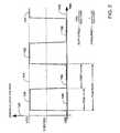
- FIG. 7illustrates a simulation timing diagram for the circuit illustrated in FIG. 5 .
- voltage FBline 293 in FIG. 5
- ramp generatorsuch as ramp generator 552 in FIG. 12
- the load voltage VOUTalso ramps ups slowly during startup at 404 .
- pulses at voltages COMP_OUT, BEFORE_TOFF and CONTROL_OUTare limited in repetition rate by a ramp generator (see FIG. 12 ) as shown at 406 , and after startup, the pulses are produced at a higher repetition rate shown at 408 that depends on a fixed time (fixed ON or fixed OFF time). Corresponding pulses appear at HG and VPWM in FIG. 5 .
- the loaddraws a power driver current of 0.2 amperes.
- the load currentabruptly changes and the power driver current increases to 1.2 amperes.
- the load currentabruptly changes again, and the power driver current decreases back to 0.2 amperes.
- Small portions of the timing diagram in FIG. 7are shown in more detail below on an expanded (zoomed) time scale in FIGS. 8-10 .
- FIG. 8illustrates a first zoomed portion of the simulation timing diagram illustrated in FIG. 7 in which the power driver current increases from 0.2 amperes to 1.2 amperes and then drops back to 0.2 amperes.
- the voltages illustrated in FIG. 8are the same voltages that are illustrated in FIG. 7 .
- a 350 microsecond time intervalis illustrated.
- a 60 microsecond zoomed intervalis illustrated.
- power driver currentchanges abruptly from 0.2 amperes to 1.2 amperes as illustrated by an abrupt drop in VOUT at 420 .
- VOUTdrops in response to the increased power driver current to a lower voltage level as illustrated at 422 , however, the ripple level remains substantially the same.
- FIG. 8illustrates a first zoomed portion of the simulation timing diagram illustrated in FIG. 7 in which the power driver current increases from 0.2 amperes to 1.2 amperes and then drops back to 0.2 amperes.
- the voltages illustrated in FIG. 8are the same voltages that are illustrated in FIG
- VOUTrises in response to the decreased power driver current to a higher voltage level as illustrated at 424 , however, the ripple level remains substantially the same, and there is very little overshoot.
- FIG. 9illustrates a further zoomed portion of the zoomed simulation timing diagram illustrated in FIG. 8 .
- the voltages and conditions illustrated in FIG. 9are the same as the voltages and conditions illustrated in FIG. 8 , however, FIG. 9 illustrates an 8 microsecond interval around the time that the power driver current changes abruptly from 0.2 to 1.2 amperes.
- a minimum off timeis maintained between pulses 430 , 432 , and pulses 430 , 432 have a fixed pulse width.
- FIG. 10illustrates a further zoomed portion of the simulation timing diagram illustrated in FIG. 8 .
- a 10 microsecond interval around the point 424 at which power driver current decreases from 1.2 to 0.2 amperesis illustrated.
- FIGS. 11A , 11 Bschematically illustrate timing diagrams that show synchronization of various signals in FIGS. 5 , 6 .
- FIG. 11Aillustrates idealized waveforms for the circuit shown in FIG. 5 .
- the comparator outputCOMP OUT
- the pulse generator outputBEFORE TOFF
- the power driverturns on and begins charging the capacitors 298 , 301 resulting in an rise, starting at 505 , in the voltage applied to the inverting input of comparator 262 .
- FIG. 12schematically illustrates an embodiment of a reference controlled by a current limit circuit to provide a soft start.
- the arrangement shown in FIG. 12is applicable to FIG. 5 , and reference numbers used in FIG. 12 that are the same as reference numbers used in FIG. 5 identify the same or similar features.
- Reference 260includes a bandgap reference 550 and a ramp generator 552 .
- the ramp generator 552can comprise an up counter 560 controlling a DAC 562 as shown.
- the ramp generator 552can also comprise alternate circuit arrangements that are known to generate a ramp output.
- a switch 554connects the bandgap reference to the non-inverting input of comparator 262 .
- a switch 556connects the ramp generator 552 to the non-inverting input of the comparator 262 .
- the switches 554 , 556are controlled using inverter 558 so that only one switch conducts at a time.
- the comparator 314triggers the logic circuit 570 to open switch 554 and close switch 556 such that the ramp generator 552 is connected to the non-inverting input of comparator 262 .
- the logic circuittriggers the ramp generator 552 to provide a ramp voltage output as a reference output during the turn-on time interval. This provides a soft start for the regulator.
- the comparator 314triggers the logic 570 to open switch 556 and close switch 554 so that the stable bandgap reference 550 is connected to the non-inverting input of the comparator 262 .
- a regulator(such as 201 ) provides a load voltage (such as 232 ).
- the regulatorincludes a power driver (such as 206 ) having a feedback input (such as 204 ) and a power driver voltage (such as at 208 ).
- the regulatorincludes a comparator (such as 214 ) having a comparator output (such as 216 ) related to a combination (such as on line 293 ) of the load voltage and the power driver current.
- the regulatorincludes a pulse generator (such as 220 ) controlled by the comparator output and having output pulses (such as 221 ) with fixed pulse widths.
- the regulatorincludes a time limit circuit (such as 225 ) controlled by the output pulses. The time limit circuit provides the output pulses to the feedback input subject to a time limit between the output pulses.
Landscapes
- Engineering & Computer Science (AREA)
- Power Engineering (AREA)
- Dc-Dc Converters (AREA)
Abstract
Description
Claims (26)
Priority Applications (1)
| Application Number | Priority Date | Filing Date | Title |
|---|---|---|---|
| US10/715,092US6906499B2 (en) | 2003-06-27 | 2003-11-17 | Current mode bang-bang controller in a switching voltage regulator |
Applications Claiming Priority (2)
| Application Number | Priority Date | Filing Date | Title |
|---|---|---|---|
| US48305203P | 2003-06-27 | 2003-06-27 | |
| US10/715,092US6906499B2 (en) | 2003-06-27 | 2003-11-17 | Current mode bang-bang controller in a switching voltage regulator |
Publications (2)
| Publication Number | Publication Date |
|---|---|
| US20040263134A1 US20040263134A1 (en) | 2004-12-30 |
| US6906499B2true US6906499B2 (en) | 2005-06-14 |
Family
ID=33544622
Family Applications (1)
| Application Number | Title | Priority Date | Filing Date |
|---|---|---|---|
| US10/715,092Expired - LifetimeUS6906499B2 (en) | 2003-06-27 | 2003-11-17 | Current mode bang-bang controller in a switching voltage regulator |
Country Status (1)
| Country | Link |
|---|---|
| US (1) | US6906499B2 (en) |
Cited By (16)
| Publication number | Priority date | Publication date | Assignee | Title |
|---|---|---|---|---|
| US20050248894A1 (en)* | 2004-05-06 | 2005-11-10 | Bliley Paul D | Voltage regulator |
| US20050269883A1 (en)* | 2004-06-02 | 2005-12-08 | Drader Marc A | Universal serial bus current limit |
| US20060091872A1 (en)* | 2004-10-28 | 2006-05-04 | Tdk Corporation | Switching power supply control device and switching power supply |
| US7157892B1 (en)* | 2005-11-28 | 2007-01-02 | Micrel, Incorporated | Robust ramp controlled enable for voltage regulator |
| US20070170884A1 (en)* | 2006-01-25 | 2007-07-26 | Jay Goetz | Switch array for use in motor control |
| US20070253229A1 (en)* | 2006-04-27 | 2007-11-01 | Dowlatabadi Ahmad B | Startup for DC/DC converters |
| US20070262826A1 (en)* | 2006-04-26 | 2007-11-15 | Dowlatabadi Ahmad B | Clock with regulated duty cycle and frequency |
| US20080018312A1 (en)* | 2005-10-24 | 2008-01-24 | Ahmad Dowlatabadi | Control Loop for Switching Power Converters |
| US20080205087A1 (en)* | 2007-02-27 | 2008-08-28 | Arlaindo Vitug Asuncion | Power supply feedback control using sensed duty cycle |
| US20090027019A1 (en)* | 2003-04-22 | 2009-01-29 | Dowlatabadi Ahmad B | Control loop for switching power converters |
| US20110163730A1 (en)* | 2010-01-06 | 2011-07-07 | Seagate Technology Llc | Current mode bang-bang regulator amplifier |
| US20110169468A1 (en)* | 2010-01-13 | 2011-07-14 | Jean-Shin Wu | Power Conversion System and Power Control Method for Reducing Cross Regulation Effect |
| US9143033B2 (en) | 2010-11-30 | 2015-09-22 | Taiwan Semiconductor Manufacturing Company, Ltd. | Hysteretic power converter with calibration circuit |
| US9838000B1 (en)* | 2016-12-22 | 2017-12-05 | Silanna Asia Pte Ltd | Minimum pulse-width assurance |
| US10033366B2 (en) | 2016-12-22 | 2018-07-24 | Silanna Asia Pte Ltd | Minimum pulse-width assurance |
| US10637351B2 (en) | 2016-07-25 | 2020-04-28 | Taiwan Semiconductor Manufacturing Co., Ltd. | Regulated voltage systems and methods using intrinsically varied process characteristics |
Families Citing this family (2)
| Publication number | Priority date | Publication date | Assignee | Title |
|---|---|---|---|---|
| JP2006067730A (en)* | 2004-08-27 | 2006-03-09 | Sanken Electric Co Ltd | Power factor improving circuit |
| IT202200000017A1 (en) | 2022-01-03 | 2023-07-03 | St Microelectronics Srl | Voltage regulator device |
Citations (15)
| Publication number | Priority date | Publication date | Assignee | Title |
|---|---|---|---|---|
| US4455526A (en) | 1982-06-29 | 1984-06-19 | The United States Of America As Represented By The Secretary Of The Air Force | FET Switching regulator |
| US5481178A (en)* | 1993-03-23 | 1996-01-02 | Linear Technology Corporation | Control circuit and method for maintaining high efficiency over broad current ranges in a switching regulator circuit |
| US5729448A (en) | 1996-10-31 | 1998-03-17 | Hewlett-Packard Company | Low cost highly manufacturable DC-to-DC power converter |
| US6057675A (en)* | 1998-05-11 | 2000-05-02 | Kabushiki Kaisha Toyoda Jidoshokki Seisakusho | DC/DC converter |
| US6057607A (en)* | 1999-07-16 | 2000-05-02 | Semtech Corporation | Method and apparatus for voltage regulation in multi-output switched mode power supplies |
| US6147478A (en) | 1999-09-17 | 2000-11-14 | Texas Instruments Incorporated | Hysteretic regulator and control method having switching frequency independent from output filter |
| US6163142A (en)* | 1998-07-08 | 2000-12-19 | Kabushiki Kaisha Toyoda Jidoshokki Seisakusho | Current-mode controller for switching DC/DC converter having a reduced output ripple current |
| US6222709B1 (en)* | 1999-02-14 | 2001-04-24 | Yazaki Corporation | Device and method for supplying electric power to a load |
| US6441681B1 (en) | 2001-06-07 | 2002-08-27 | Texas Instruments Incorporated | Method for preserving charges on a cap at the output of a regulator |
| US6456050B1 (en)* | 2001-11-05 | 2002-09-24 | Dan Agiman | Virtual frequency-controlled switching voltage regulator |
| US6476589B2 (en)* | 2001-04-06 | 2002-11-05 | Linear Technology Corporation | Circuits and methods for synchronizing non-constant frequency switching regulators with a phase locked loop |
| US20020180410A1 (en) | 2000-11-07 | 2002-12-05 | Brooks Steven W. | Switching regulator with transient recovery circuit |
| US20030090253A1 (en) | 2001-11-13 | 2003-05-15 | Balu Balakrishnan | Method and apparatus for a switch mode power supply that generates a high pulse width modulation while maintaining low noise sensitivity |
| US20030142519A1 (en) | 2002-01-29 | 2003-07-31 | Intersil Americas Inc. | Synthetic ripple regulator |
| US20030151929A1 (en) | 2002-01-28 | 2003-08-14 | Salvador Figueroa | Power converter with input-side resonance and pulse-position demodulation feedback control |
Family Cites Families (1)
| Publication number | Priority date | Publication date | Assignee | Title |
|---|---|---|---|---|
| US4541288A (en)* | 1983-10-27 | 1985-09-17 | General Electric Company | Operating circuit for magnetoelastic force/pressure sensors |
- 2003
- 2003-11-17USUS10/715,092patent/US6906499B2/ennot_activeExpired - Lifetime
Patent Citations (17)
| Publication number | Priority date | Publication date | Assignee | Title |
|---|---|---|---|---|
| US4455526A (en) | 1982-06-29 | 1984-06-19 | The United States Of America As Represented By The Secretary Of The Air Force | FET Switching regulator |
| US5481178A (en)* | 1993-03-23 | 1996-01-02 | Linear Technology Corporation | Control circuit and method for maintaining high efficiency over broad current ranges in a switching regulator circuit |
| US6304066B1 (en)* | 1993-03-23 | 2001-10-16 | Linear Technology Corporation | Control circuit and method for maintaining high efficiency over broad current ranges in a switching regular circuit |
| US5729448A (en) | 1996-10-31 | 1998-03-17 | Hewlett-Packard Company | Low cost highly manufacturable DC-to-DC power converter |
| US6057675A (en)* | 1998-05-11 | 2000-05-02 | Kabushiki Kaisha Toyoda Jidoshokki Seisakusho | DC/DC converter |
| US6163142A (en)* | 1998-07-08 | 2000-12-19 | Kabushiki Kaisha Toyoda Jidoshokki Seisakusho | Current-mode controller for switching DC/DC converter having a reduced output ripple current |
| US6222709B1 (en)* | 1999-02-14 | 2001-04-24 | Yazaki Corporation | Device and method for supplying electric power to a load |
| US6057607A (en)* | 1999-07-16 | 2000-05-02 | Semtech Corporation | Method and apparatus for voltage regulation in multi-output switched mode power supplies |
| US6147478A (en) | 1999-09-17 | 2000-11-14 | Texas Instruments Incorporated | Hysteretic regulator and control method having switching frequency independent from output filter |
| US20020180410A1 (en) | 2000-11-07 | 2002-12-05 | Brooks Steven W. | Switching regulator with transient recovery circuit |
| US6476589B2 (en)* | 2001-04-06 | 2002-11-05 | Linear Technology Corporation | Circuits and methods for synchronizing non-constant frequency switching regulators with a phase locked loop |
| US6774611B2 (en)* | 2001-04-06 | 2004-08-10 | Linear Technology Corporation | Circuits and methods for synchronizing non-constant frequency switching regulators with a phase locked loop |
| US6441681B1 (en) | 2001-06-07 | 2002-08-27 | Texas Instruments Incorporated | Method for preserving charges on a cap at the output of a regulator |
| US6456050B1 (en)* | 2001-11-05 | 2002-09-24 | Dan Agiman | Virtual frequency-controlled switching voltage regulator |
| US20030090253A1 (en) | 2001-11-13 | 2003-05-15 | Balu Balakrishnan | Method and apparatus for a switch mode power supply that generates a high pulse width modulation while maintaining low noise sensitivity |
| US20030151929A1 (en) | 2002-01-28 | 2003-08-14 | Salvador Figueroa | Power converter with input-side resonance and pulse-position demodulation feedback control |
| US20030142519A1 (en) | 2002-01-29 | 2003-07-31 | Intersil Americas Inc. | Synthetic ripple regulator |
Cited By (33)
| Publication number | Priority date | Publication date | Assignee | Title |
|---|---|---|---|---|
| US8604768B2 (en) | 2003-04-22 | 2013-12-10 | Aivaka, Inc | Control loop for switching power converters |
| US20090027019A1 (en)* | 2003-04-22 | 2009-01-29 | Dowlatabadi Ahmad B | Control loop for switching power converters |
| US8427127B2 (en) | 2003-04-22 | 2013-04-23 | Aivaka, Inc. | Control loop for switching power converters |
| US20050248894A1 (en)* | 2004-05-06 | 2005-11-10 | Bliley Paul D | Voltage regulator |
| US7515393B2 (en)* | 2004-05-06 | 2009-04-07 | Hewlett-Packard Development Company, L.P. | Voltage regulator |
| US20050269883A1 (en)* | 2004-06-02 | 2005-12-08 | Drader Marc A | Universal serial bus current limit |
| US8378527B2 (en)* | 2004-06-02 | 2013-02-19 | Research In Motion Limited | Universal serial bus current limit |
| US7132818B2 (en)* | 2004-10-28 | 2006-11-07 | Tdk Corporation | Switching power supply control device and switching power supply |
| US20060091872A1 (en)* | 2004-10-28 | 2006-05-04 | Tdk Corporation | Switching power supply control device and switching power supply |
| US20080018312A1 (en)* | 2005-10-24 | 2008-01-24 | Ahmad Dowlatabadi | Control Loop for Switching Power Converters |
| US7157892B1 (en)* | 2005-11-28 | 2007-01-02 | Micrel, Incorporated | Robust ramp controlled enable for voltage regulator |
| US8796969B2 (en)* | 2006-01-25 | 2014-08-05 | International Rectifier Corporation | Switch array for use in motor control |
| US20070170884A1 (en)* | 2006-01-25 | 2007-07-26 | Jay Goetz | Switch array for use in motor control |
| US8264266B2 (en) | 2006-04-26 | 2012-09-11 | Aivaka, Inc. | Clock with regulated duty cycle and frequency |
| US20070262826A1 (en)* | 2006-04-26 | 2007-11-15 | Dowlatabadi Ahmad B | Clock with regulated duty cycle and frequency |
| US20070253229A1 (en)* | 2006-04-27 | 2007-11-01 | Dowlatabadi Ahmad B | Startup for DC/DC converters |
| US8797010B2 (en)* | 2006-04-27 | 2014-08-05 | Aivaka, Inc. | Startup for DC/DC converters |
| US20080205087A1 (en)* | 2007-02-27 | 2008-08-28 | Arlaindo Vitug Asuncion | Power supply feedback control using sensed duty cycle |
| US20110163730A1 (en)* | 2010-01-06 | 2011-07-07 | Seagate Technology Llc | Current mode bang-bang regulator amplifier |
| US8222873B2 (en) | 2010-01-06 | 2012-07-17 | Seagate Technology Llc | Current mode bang-bang regulator amplifier |
| US20110169468A1 (en)* | 2010-01-13 | 2011-07-14 | Jean-Shin Wu | Power Conversion System and Power Control Method for Reducing Cross Regulation Effect |
| US8258767B2 (en)* | 2010-01-13 | 2012-09-04 | Alpha & Omega Semiconductor, Inc. | Power conversion system and power control method for reducing cross regulation effect |
| US8502509B2 (en)* | 2010-04-30 | 2013-08-06 | Alpha & Omega Semiconductor, Inc. | Power conversion system and power control method for reducing cross regulation effect |
| US20120299567A1 (en)* | 2010-04-30 | 2012-11-29 | Jean-Shin Wu | Power Conversion System and Power Control Method for Reducing Cross Regulation Effect |
| US9143033B2 (en) | 2010-11-30 | 2015-09-22 | Taiwan Semiconductor Manufacturing Company, Ltd. | Hysteretic power converter with calibration circuit |
| US10082811B2 (en) | 2010-11-30 | 2018-09-25 | Taiwan Semiconductor Manufacturing Company, Ltd. | Hysteretic power converter with calibration circuit |
| US11239749B2 (en) | 2016-07-25 | 2022-02-01 | Taiwan Semiconductor Manufacturing Co., Ltd. | Regulated voltage systems and methods using intrinsically varied process characteristics |
| US11909312B2 (en) | 2016-07-25 | 2024-02-20 | Taiwan Semiconductor Manufacturing Co., Ltd. | Regulated voltage systems and methods using intrinsically varied process characteristics |
| US11606027B2 (en) | 2016-07-25 | 2023-03-14 | Taiwan Semiconductor Manufacturing Co., Ltd. | Regulated voltage systems and methods using intrinsically varied process characteristics |
| US10637351B2 (en) | 2016-07-25 | 2020-04-28 | Taiwan Semiconductor Manufacturing Co., Ltd. | Regulated voltage systems and methods using intrinsically varied process characteristics |
| US9838000B1 (en)* | 2016-12-22 | 2017-12-05 | Silanna Asia Pte Ltd | Minimum pulse-width assurance |
| US10250244B2 (en) | 2016-12-22 | 2019-04-02 | Silanna Asia Pte Ltd | Minimum pulse-width assurance |
| US10033366B2 (en) | 2016-12-22 | 2018-07-24 | Silanna Asia Pte Ltd | Minimum pulse-width assurance |
Also Published As
| Publication number | Publication date |
|---|---|
| US20040263134A1 (en) | 2004-12-30 |
Similar Documents
| Publication | Publication Date | Title |
|---|---|---|
| US6906499B2 (en) | Current mode bang-bang controller in a switching voltage regulator | |
| US8232790B2 (en) | Architecture for controlling a dual polarity, single inductor boost regulator used as a dual polarity supply in a hard disk drive dual stage actuator (DSA) device | |
| US6757129B2 (en) | Magnetic disk storage apparatus | |
| US7863841B2 (en) | Class H drive | |
| US8115563B2 (en) | Pulse width modulation circuit and voltage-feedback class-D amplifier circuit | |
| US7262588B2 (en) | Method and apparatus for power supply controlling capable of effectively controlling switching operations | |
| US7453287B2 (en) | Switching power-supply circuit and semiconductor integrated circuit | |
| US7453251B1 (en) | Voltage tracking reference for a power regulator | |
| US9667142B2 (en) | Power supply device with shared inductive elements under switch control | |
| US20020145413A1 (en) | DC-DC converter and storage apparatus | |
| US7294993B2 (en) | Method and apparatus for customizing of a power supply based on load characteristic data | |
| US7615982B1 (en) | Power converter able to rapidly respond to fast changes in load current | |
| TWI364156B (en) | ||
| US20080265822A1 (en) | Class G motor drive | |
| US8159202B2 (en) | Quasi-continuous voltage regulator with dual polarity outputs | |
| CN101034848A (en) | Voltage regulating systems responsive to feed-forward information from deterministic loads | |
| JP2006006004A (en) | Buck-boost DC-DC converter | |
| US20110057635A1 (en) | Switching regulator | |
| US11037596B2 (en) | Motor driver device and semiconductor device | |
| US8791657B2 (en) | Disk drive | |
| US8232788B2 (en) | Quasi-continuous voltage regulator and controller | |
| EP1759383B1 (en) | Rejection of power supply variations for gain error cancellation in pulse-width-modulated motor controllers | |
| US6643087B1 (en) | Disk drive with improved retract circuit and method | |
| US6771480B2 (en) | Circuit to sample and compare the BEMF on an actuator into a constant velocity control | |
| US20100067140A1 (en) | Disk-Drive Read/Write Head Retraction Velocity Control |
Legal Events
| Date | Code | Title | Description |
|---|---|---|---|
| AS | Assignment | Owner name:SEAGATE TECHNOLOGY LLC, CALIFORNIA Free format text:ASSIGNMENT OF ASSIGNORS INTEREST;ASSIGNORS:HUSSEIN, HAKAM D.;ZHANG, WENDONG;REEL/FRAME:014713/0164 Effective date:20031107 | |
| STCF | Information on status: patent grant | Free format text:PATENTED CASE | |
| FPAY | Fee payment | Year of fee payment:4 | |
| AS | Assignment | Owner name:WELLS FARGO BANK, NATIONAL ASSOCIATION, AS COLLATERAL AGENT AND SECOND PRIORITY REPRESENTATIVE, CALIFORNIA Free format text:SECURITY AGREEMENT;ASSIGNORS:MAXTOR CORPORATION;SEAGATE TECHNOLOGY LLC;SEAGATE TECHNOLOGY INTERNATIONAL;REEL/FRAME:022757/0017 Effective date:20090507 Owner name:JPMORGAN CHASE BANK, N.A., AS ADMINISTRATIVE AGENT AND FIRST PRIORITY REPRESENTATIVE, NEW YORK Free format text:SECURITY AGREEMENT;ASSIGNORS:MAXTOR CORPORATION;SEAGATE TECHNOLOGY LLC;SEAGATE TECHNOLOGY INTERNATIONAL;REEL/FRAME:022757/0017 Effective date:20090507 Owner name:JPMORGAN CHASE BANK, N.A., AS ADMINISTRATIVE AGENT Free format text:SECURITY AGREEMENT;ASSIGNORS:MAXTOR CORPORATION;SEAGATE TECHNOLOGY LLC;SEAGATE TECHNOLOGY INTERNATIONAL;REEL/FRAME:022757/0017 Effective date:20090507 Owner name:WELLS FARGO BANK, NATIONAL ASSOCIATION, AS COLLATE Free format text:SECURITY AGREEMENT;ASSIGNORS:MAXTOR CORPORATION;SEAGATE TECHNOLOGY LLC;SEAGATE TECHNOLOGY INTERNATIONAL;REEL/FRAME:022757/0017 Effective date:20090507 | |
| AS | Assignment | Owner name:SEAGATE TECHNOLOGY HDD HOLDINGS, CALIFORNIA Free format text:RELEASE;ASSIGNOR:JPMORGAN CHASE BANK, N.A., AS ADMINISTRATIVE AGENT;REEL/FRAME:025662/0001 Effective date:20110114 Owner name:SEAGATE TECHNOLOGY LLC, CALIFORNIA Free format text:RELEASE;ASSIGNOR:JPMORGAN CHASE BANK, N.A., AS ADMINISTRATIVE AGENT;REEL/FRAME:025662/0001 Effective date:20110114 Owner name:SEAGATE TECHNOLOGY INTERNATIONAL, CALIFORNIA Free format text:RELEASE;ASSIGNOR:JPMORGAN CHASE BANK, N.A., AS ADMINISTRATIVE AGENT;REEL/FRAME:025662/0001 Effective date:20110114 Owner name:MAXTOR CORPORATION, CALIFORNIA Free format text:RELEASE;ASSIGNOR:JPMORGAN CHASE BANK, N.A., AS ADMINISTRATIVE AGENT;REEL/FRAME:025662/0001 Effective date:20110114 | |
| AS | Assignment | Owner name:THE BANK OF NOVA SCOTIA, AS ADMINISTRATIVE AGENT, CANADA Free format text:SECURITY AGREEMENT;ASSIGNOR:SEAGATE TECHNOLOGY LLC;REEL/FRAME:026010/0350 Effective date:20110118 Owner name:THE BANK OF NOVA SCOTIA, AS ADMINISTRATIVE AGENT, Free format text:SECURITY AGREEMENT;ASSIGNOR:SEAGATE TECHNOLOGY LLC;REEL/FRAME:026010/0350 Effective date:20110118 | |
| FPAY | Fee payment | Year of fee payment:8 | |
| AS | Assignment | Owner name:SEAGATE TECHNOLOGY INTERNATIONAL, CAYMAN ISLANDS Free format text:TERMINATION AND RELEASE OF SECURITY INTEREST IN PATENT RIGHTS;ASSIGNOR:WELLS FARGO BANK, NATIONAL ASSOCIATION, AS COLLATERAL AGENT AND SECOND PRIORITY REPRESENTATIVE;REEL/FRAME:030833/0001 Effective date:20130312 Owner name:SEAGATE TECHNOLOGY LLC, CALIFORNIA Free format text:TERMINATION AND RELEASE OF SECURITY INTEREST IN PATENT RIGHTS;ASSIGNOR:WELLS FARGO BANK, NATIONAL ASSOCIATION, AS COLLATERAL AGENT AND SECOND PRIORITY REPRESENTATIVE;REEL/FRAME:030833/0001 Effective date:20130312 Owner name:EVAULT INC. (F/K/A I365 INC.), CALIFORNIA Free format text:TERMINATION AND RELEASE OF SECURITY INTEREST IN PATENT RIGHTS;ASSIGNOR:WELLS FARGO BANK, NATIONAL ASSOCIATION, AS COLLATERAL AGENT AND SECOND PRIORITY REPRESENTATIVE;REEL/FRAME:030833/0001 Effective date:20130312 Owner name:SEAGATE TECHNOLOGY US HOLDINGS, INC., CALIFORNIA Free format text:TERMINATION AND RELEASE OF SECURITY INTEREST IN PATENT RIGHTS;ASSIGNOR:WELLS FARGO BANK, NATIONAL ASSOCIATION, AS COLLATERAL AGENT AND SECOND PRIORITY REPRESENTATIVE;REEL/FRAME:030833/0001 Effective date:20130312 | |
| FPAY | Fee payment | Year of fee payment:12 | |
| AS | Assignment | Owner name:SEAGATE TECHNOLOGY PUBLIC LIMITED COMPANY, CALIFORNIA Free format text:RELEASE BY SECURED PARTY;ASSIGNOR:THE BANK OF NOVA SCOTIA;REEL/FRAME:072193/0001 Effective date:20250303 Owner name:SEAGATE TECHNOLOGY, CALIFORNIA Free format text:RELEASE BY SECURED PARTY;ASSIGNOR:THE BANK OF NOVA SCOTIA;REEL/FRAME:072193/0001 Effective date:20250303 Owner name:SEAGATE TECHNOLOGY HDD HOLDINGS, CALIFORNIA Free format text:RELEASE BY SECURED PARTY;ASSIGNOR:THE BANK OF NOVA SCOTIA;REEL/FRAME:072193/0001 Effective date:20250303 Owner name:I365 INC., CALIFORNIA Free format text:RELEASE BY SECURED PARTY;ASSIGNOR:THE BANK OF NOVA SCOTIA;REEL/FRAME:072193/0001 Effective date:20250303 Owner name:SEAGATE TECHNOLOGY LLC, CALIFORNIA Free format text:RELEASE BY SECURED PARTY;ASSIGNOR:THE BANK OF NOVA SCOTIA;REEL/FRAME:072193/0001 Effective date:20250303 Owner name:SEAGATE TECHNOLOGY INTERNATIONAL, CAYMAN ISLANDS Free format text:RELEASE BY SECURED PARTY;ASSIGNOR:THE BANK OF NOVA SCOTIA;REEL/FRAME:072193/0001 Effective date:20250303 Owner name:SEAGATE HDD CAYMAN, CAYMAN ISLANDS Free format text:RELEASE BY SECURED PARTY;ASSIGNOR:THE BANK OF NOVA SCOTIA;REEL/FRAME:072193/0001 Effective date:20250303 Owner name:SEAGATE TECHNOLOGY (US) HOLDINGS, INC., CALIFORNIA Free format text:RELEASE BY SECURED PARTY;ASSIGNOR:THE BANK OF NOVA SCOTIA;REEL/FRAME:072193/0001 Effective date:20250303 |