US6906408B2 - Assemblies and packages including die-to-die connections - Google Patents
Assemblies and packages including die-to-die connectionsDownload PDFInfo
- Publication number
- US6906408B2 US6906408B2US10/382,025US38202503AUS6906408B2US 6906408 B2US6906408 B2US 6906408B2US 38202503 AUS38202503 AUS 38202503AUS 6906408 B2US6906408 B2US 6906408B2
- Authority
- US
- United States
- Prior art keywords
- semiconductor die
- semiconductor
- bond pads
- assembly
- device package
- Prior art date
- Legal status (The legal status is an assumption and is not a legal conclusion. Google has not performed a legal analysis and makes no representation as to the accuracy of the status listed.)
- Expired - Lifetime
Links
Images


Classifications
- H—ELECTRICITY
- H01—ELECTRIC ELEMENTS
- H01L—SEMICONDUCTOR DEVICES NOT COVERED BY CLASS H10
- H01L25/00—Assemblies consisting of a plurality of semiconductor or other solid state devices
- H01L25/50—Multistep manufacturing processes of assemblies consisting of devices, the devices being individual devices of subclass H10D or integrated devices of class H10
- H—ELECTRICITY
- H01—ELECTRIC ELEMENTS
- H01L—SEMICONDUCTOR DEVICES NOT COVERED BY CLASS H10
- H01L25/00—Assemblies consisting of a plurality of semiconductor or other solid state devices
- H01L25/03—Assemblies consisting of a plurality of semiconductor or other solid state devices all the devices being of a type provided for in a single subclass of subclasses H10B, H10D, H10F, H10H, H10K or H10N, e.g. assemblies of rectifier diodes
- H01L25/04—Assemblies consisting of a plurality of semiconductor or other solid state devices all the devices being of a type provided for in a single subclass of subclasses H10B, H10D, H10F, H10H, H10K or H10N, e.g. assemblies of rectifier diodes the devices not having separate containers
- H01L25/065—Assemblies consisting of a plurality of semiconductor or other solid state devices all the devices being of a type provided for in a single subclass of subclasses H10B, H10D, H10F, H10H, H10K or H10N, e.g. assemblies of rectifier diodes the devices not having separate containers the devices being of a type provided for in group H10D89/00
- H01L25/0652—Assemblies consisting of a plurality of semiconductor or other solid state devices all the devices being of a type provided for in a single subclass of subclasses H10B, H10D, H10F, H10H, H10K or H10N, e.g. assemblies of rectifier diodes the devices not having separate containers the devices being of a type provided for in group H10D89/00 the devices being arranged next and on each other, i.e. mixed assemblies
- B—PERFORMING OPERATIONS; TRANSPORTING
- B33—ADDITIVE MANUFACTURING TECHNOLOGY
- B33Y—ADDITIVE MANUFACTURING, i.e. MANUFACTURING OF THREE-DIMENSIONAL [3-D] OBJECTS BY ADDITIVE DEPOSITION, ADDITIVE AGGLOMERATION OR ADDITIVE LAYERING, e.g. BY 3-D PRINTING, STEREOLITHOGRAPHY OR SELECTIVE LASER SINTERING
- B33Y80/00—Products made by additive manufacturing
- H—ELECTRICITY
- H01—ELECTRIC ELEMENTS
- H01L—SEMICONDUCTOR DEVICES NOT COVERED BY CLASS H10
- H01L2224/00—Indexing scheme for arrangements for connecting or disconnecting semiconductor or solid-state bodies and methods related thereto as covered by H01L24/00
- H01L2224/01—Means for bonding being attached to, or being formed on, the surface to be connected, e.g. chip-to-package, die-attach, "first-level" interconnects; Manufacturing methods related thereto
- H01L2224/02—Bonding areas; Manufacturing methods related thereto
- H01L2224/04—Structure, shape, material or disposition of the bonding areas prior to the connecting process
- H01L2224/05—Structure, shape, material or disposition of the bonding areas prior to the connecting process of an individual bonding area
- H01L2224/05001—Internal layers
- H01L2224/0502—Disposition
- H01L2224/05026—Disposition the internal layer being disposed in a recess of the surface
- H—ELECTRICITY
- H01—ELECTRIC ELEMENTS
- H01L—SEMICONDUCTOR DEVICES NOT COVERED BY CLASS H10
- H01L2224/00—Indexing scheme for arrangements for connecting or disconnecting semiconductor or solid-state bodies and methods related thereto as covered by H01L24/00
- H01L2224/01—Means for bonding being attached to, or being formed on, the surface to be connected, e.g. chip-to-package, die-attach, "first-level" interconnects; Manufacturing methods related thereto
- H01L2224/02—Bonding areas; Manufacturing methods related thereto
- H01L2224/04—Structure, shape, material or disposition of the bonding areas prior to the connecting process
- H01L2224/05—Structure, shape, material or disposition of the bonding areas prior to the connecting process of an individual bonding area
- H01L2224/05001—Internal layers
- H01L2224/05075—Plural internal layers
- H01L2224/0508—Plural internal layers being stacked
- H—ELECTRICITY
- H01—ELECTRIC ELEMENTS
- H01L—SEMICONDUCTOR DEVICES NOT COVERED BY CLASS H10
- H01L2224/00—Indexing scheme for arrangements for connecting or disconnecting semiconductor or solid-state bodies and methods related thereto as covered by H01L24/00
- H01L2224/01—Means for bonding being attached to, or being formed on, the surface to be connected, e.g. chip-to-package, die-attach, "first-level" interconnects; Manufacturing methods related thereto
- H01L2224/02—Bonding areas; Manufacturing methods related thereto
- H01L2224/04—Structure, shape, material or disposition of the bonding areas prior to the connecting process
- H01L2224/05—Structure, shape, material or disposition of the bonding areas prior to the connecting process of an individual bonding area
- H01L2224/0554—External layer
- H01L2224/0556—Disposition
- H01L2224/05571—Disposition the external layer being disposed in a recess of the surface
- H—ELECTRICITY
- H01—ELECTRIC ELEMENTS
- H01L—SEMICONDUCTOR DEVICES NOT COVERED BY CLASS H10
- H01L2224/00—Indexing scheme for arrangements for connecting or disconnecting semiconductor or solid-state bodies and methods related thereto as covered by H01L24/00
- H01L2224/01—Means for bonding being attached to, or being formed on, the surface to be connected, e.g. chip-to-package, die-attach, "first-level" interconnects; Manufacturing methods related thereto
- H01L2224/02—Bonding areas; Manufacturing methods related thereto
- H01L2224/04—Structure, shape, material or disposition of the bonding areas prior to the connecting process
- H01L2224/05—Structure, shape, material or disposition of the bonding areas prior to the connecting process of an individual bonding area
- H01L2224/0554—External layer
- H01L2224/05573—Single external layer
- H—ELECTRICITY
- H01—ELECTRIC ELEMENTS
- H01L—SEMICONDUCTOR DEVICES NOT COVERED BY CLASS H10
- H01L2224/00—Indexing scheme for arrangements for connecting or disconnecting semiconductor or solid-state bodies and methods related thereto as covered by H01L24/00
- H01L2224/01—Means for bonding being attached to, or being formed on, the surface to be connected, e.g. chip-to-package, die-attach, "first-level" interconnects; Manufacturing methods related thereto
- H01L2224/02—Bonding areas; Manufacturing methods related thereto
- H01L2224/04—Structure, shape, material or disposition of the bonding areas prior to the connecting process
- H01L2224/06—Structure, shape, material or disposition of the bonding areas prior to the connecting process of a plurality of bonding areas
- H01L2224/061—Disposition
- H01L2224/0612—Layout
- H01L2224/0613—Square or rectangular array
- H01L2224/06131—Square or rectangular array being uniform, i.e. having a uniform pitch across the array
- H—ELECTRICITY
- H01—ELECTRIC ELEMENTS
- H01L—SEMICONDUCTOR DEVICES NOT COVERED BY CLASS H10
- H01L2224/00—Indexing scheme for arrangements for connecting or disconnecting semiconductor or solid-state bodies and methods related thereto as covered by H01L24/00
- H01L2224/01—Means for bonding being attached to, or being formed on, the surface to be connected, e.g. chip-to-package, die-attach, "first-level" interconnects; Manufacturing methods related thereto
- H01L2224/10—Bump connectors; Manufacturing methods related thereto
- H01L2224/15—Structure, shape, material or disposition of the bump connectors after the connecting process
- H01L2224/16—Structure, shape, material or disposition of the bump connectors after the connecting process of an individual bump connector
- H01L2224/161—Disposition
- H01L2224/16135—Disposition the bump connector connecting between different semiconductor or solid-state bodies, i.e. chip-to-chip
- H01L2224/16145—Disposition the bump connector connecting between different semiconductor or solid-state bodies, i.e. chip-to-chip the bodies being stacked
- H—ELECTRICITY
- H01—ELECTRIC ELEMENTS
- H01L—SEMICONDUCTOR DEVICES NOT COVERED BY CLASS H10
- H01L2224/00—Indexing scheme for arrangements for connecting or disconnecting semiconductor or solid-state bodies and methods related thereto as covered by H01L24/00
- H01L2224/01—Means for bonding being attached to, or being formed on, the surface to be connected, e.g. chip-to-package, die-attach, "first-level" interconnects; Manufacturing methods related thereto
- H01L2224/10—Bump connectors; Manufacturing methods related thereto
- H01L2224/15—Structure, shape, material or disposition of the bump connectors after the connecting process
- H01L2224/16—Structure, shape, material or disposition of the bump connectors after the connecting process of an individual bump connector
- H01L2224/161—Disposition
- H01L2224/16151—Disposition the bump connector connecting between a semiconductor or solid-state body and an item not being a semiconductor or solid-state body, e.g. chip-to-substrate, chip-to-passive
- H01L2224/16221—Disposition the bump connector connecting between a semiconductor or solid-state body and an item not being a semiconductor or solid-state body, e.g. chip-to-substrate, chip-to-passive the body and the item being stacked
- H01L2224/16225—Disposition the bump connector connecting between a semiconductor or solid-state body and an item not being a semiconductor or solid-state body, e.g. chip-to-substrate, chip-to-passive the body and the item being stacked the item being non-metallic, e.g. insulating substrate with or without metallisation
- H01L2224/16227—Disposition the bump connector connecting between a semiconductor or solid-state body and an item not being a semiconductor or solid-state body, e.g. chip-to-substrate, chip-to-passive the body and the item being stacked the item being non-metallic, e.g. insulating substrate with or without metallisation the bump connector connecting to a bond pad of the item
- H—ELECTRICITY
- H01—ELECTRIC ELEMENTS
- H01L—SEMICONDUCTOR DEVICES NOT COVERED BY CLASS H10
- H01L2224/00—Indexing scheme for arrangements for connecting or disconnecting semiconductor or solid-state bodies and methods related thereto as covered by H01L24/00
- H01L2224/01—Means for bonding being attached to, or being formed on, the surface to be connected, e.g. chip-to-package, die-attach, "first-level" interconnects; Manufacturing methods related thereto
- H01L2224/10—Bump connectors; Manufacturing methods related thereto
- H01L2224/15—Structure, shape, material or disposition of the bump connectors after the connecting process
- H01L2224/16—Structure, shape, material or disposition of the bump connectors after the connecting process of an individual bump connector
- H01L2224/161—Disposition
- H01L2224/16151—Disposition the bump connector connecting between a semiconductor or solid-state body and an item not being a semiconductor or solid-state body, e.g. chip-to-substrate, chip-to-passive
- H01L2224/16221—Disposition the bump connector connecting between a semiconductor or solid-state body and an item not being a semiconductor or solid-state body, e.g. chip-to-substrate, chip-to-passive the body and the item being stacked
- H01L2224/16225—Disposition the bump connector connecting between a semiconductor or solid-state body and an item not being a semiconductor or solid-state body, e.g. chip-to-substrate, chip-to-passive the body and the item being stacked the item being non-metallic, e.g. insulating substrate with or without metallisation
- H01L2224/16237—Disposition the bump connector connecting between a semiconductor or solid-state body and an item not being a semiconductor or solid-state body, e.g. chip-to-substrate, chip-to-passive the body and the item being stacked the item being non-metallic, e.g. insulating substrate with or without metallisation the bump connector connecting to a bonding area disposed in a recess of the surface of the item
- H—ELECTRICITY
- H01—ELECTRIC ELEMENTS
- H01L—SEMICONDUCTOR DEVICES NOT COVERED BY CLASS H10
- H01L2224/00—Indexing scheme for arrangements for connecting or disconnecting semiconductor or solid-state bodies and methods related thereto as covered by H01L24/00
- H01L2224/01—Means for bonding being attached to, or being formed on, the surface to be connected, e.g. chip-to-package, die-attach, "first-level" interconnects; Manufacturing methods related thereto
- H01L2224/10—Bump connectors; Manufacturing methods related thereto
- H01L2224/15—Structure, shape, material or disposition of the bump connectors after the connecting process
- H01L2224/16—Structure, shape, material or disposition of the bump connectors after the connecting process of an individual bump connector
- H01L2224/161—Disposition
- H01L2224/16151—Disposition the bump connector connecting between a semiconductor or solid-state body and an item not being a semiconductor or solid-state body, e.g. chip-to-substrate, chip-to-passive
- H01L2224/16221—Disposition the bump connector connecting between a semiconductor or solid-state body and an item not being a semiconductor or solid-state body, e.g. chip-to-substrate, chip-to-passive the body and the item being stacked
- H01L2224/16245—Disposition the bump connector connecting between a semiconductor or solid-state body and an item not being a semiconductor or solid-state body, e.g. chip-to-substrate, chip-to-passive the body and the item being stacked the item being metallic
- H—ELECTRICITY
- H01—ELECTRIC ELEMENTS
- H01L—SEMICONDUCTOR DEVICES NOT COVERED BY CLASS H10
- H01L2224/00—Indexing scheme for arrangements for connecting or disconnecting semiconductor or solid-state bodies and methods related thereto as covered by H01L24/00
- H01L2224/01—Means for bonding being attached to, or being formed on, the surface to be connected, e.g. chip-to-package, die-attach, "first-level" interconnects; Manufacturing methods related thereto
- H01L2224/10—Bump connectors; Manufacturing methods related thereto
- H01L2224/15—Structure, shape, material or disposition of the bump connectors after the connecting process
- H01L2224/17—Structure, shape, material or disposition of the bump connectors after the connecting process of a plurality of bump connectors
- H01L2224/1701—Structure
- H01L2224/1703—Bump connectors having different sizes, e.g. different diameters, heights or widths
- H—ELECTRICITY
- H01—ELECTRIC ELEMENTS
- H01L—SEMICONDUCTOR DEVICES NOT COVERED BY CLASS H10
- H01L2224/00—Indexing scheme for arrangements for connecting or disconnecting semiconductor or solid-state bodies and methods related thereto as covered by H01L24/00
- H01L2224/73—Means for bonding being of different types provided for in two or more of groups H01L2224/10, H01L2224/18, H01L2224/26, H01L2224/34, H01L2224/42, H01L2224/50, H01L2224/63, H01L2224/71
- H01L2224/732—Location after the connecting process
- H01L2224/73251—Location after the connecting process on different surfaces
- H01L2224/73253—Bump and layer connectors
- H—ELECTRICITY
- H01—ELECTRIC ELEMENTS
- H01L—SEMICONDUCTOR DEVICES NOT COVERED BY CLASS H10
- H01L2224/00—Indexing scheme for arrangements for connecting or disconnecting semiconductor or solid-state bodies and methods related thereto as covered by H01L24/00
- H01L2224/80—Methods for connecting semiconductor or other solid state bodies using means for bonding being attached to, or being formed on, the surface to be connected
- H01L2224/81—Methods for connecting semiconductor or other solid state bodies using means for bonding being attached to, or being formed on, the surface to be connected using a bump connector
- H01L2224/8112—Aligning
- H01L2224/81136—Aligning involving guiding structures, e.g. spacers or supporting members
- H—ELECTRICITY
- H01—ELECTRIC ELEMENTS
- H01L—SEMICONDUCTOR DEVICES NOT COVERED BY CLASS H10
- H01L2224/00—Indexing scheme for arrangements for connecting or disconnecting semiconductor or solid-state bodies and methods related thereto as covered by H01L24/00
- H01L2224/80—Methods for connecting semiconductor or other solid state bodies using means for bonding being attached to, or being formed on, the surface to be connected
- H01L2224/81—Methods for connecting semiconductor or other solid state bodies using means for bonding being attached to, or being formed on, the surface to be connected using a bump connector
- H01L2224/8119—Arrangement of the bump connectors prior to mounting
- H01L2224/81191—Arrangement of the bump connectors prior to mounting wherein the bump connectors are disposed only on the semiconductor or solid-state body
- H—ELECTRICITY
- H01—ELECTRIC ELEMENTS
- H01L—SEMICONDUCTOR DEVICES NOT COVERED BY CLASS H10
- H01L2224/00—Indexing scheme for arrangements for connecting or disconnecting semiconductor or solid-state bodies and methods related thereto as covered by H01L24/00
- H01L2224/80—Methods for connecting semiconductor or other solid state bodies using means for bonding being attached to, or being formed on, the surface to be connected
- H01L2224/81—Methods for connecting semiconductor or other solid state bodies using means for bonding being attached to, or being formed on, the surface to be connected using a bump connector
- H01L2224/8119—Arrangement of the bump connectors prior to mounting
- H01L2224/81193—Arrangement of the bump connectors prior to mounting wherein the bump connectors are disposed on both the semiconductor or solid-state body and another item or body to be connected to the semiconductor or solid-state body
- H—ELECTRICITY
- H01—ELECTRIC ELEMENTS
- H01L—SEMICONDUCTOR DEVICES NOT COVERED BY CLASS H10
- H01L24/00—Arrangements for connecting or disconnecting semiconductor or solid-state bodies; Methods or apparatus related thereto
- H01L24/01—Means for bonding being attached to, or being formed on, the surface to be connected, e.g. chip-to-package, die-attach, "first-level" interconnects; Manufacturing methods related thereto
- H01L24/02—Bonding areas ; Manufacturing methods related thereto
- H01L24/04—Structure, shape, material or disposition of the bonding areas prior to the connecting process
- H01L24/05—Structure, shape, material or disposition of the bonding areas prior to the connecting process of an individual bonding area
- H—ELECTRICITY
- H01—ELECTRIC ELEMENTS
- H01L—SEMICONDUCTOR DEVICES NOT COVERED BY CLASS H10
- H01L2924/00—Indexing scheme for arrangements or methods for connecting or disconnecting semiconductor or solid-state bodies as covered by H01L24/00
- H01L2924/0001—Technical content checked by a classifier
- H01L2924/00014—Technical content checked by a classifier the subject-matter covered by the group, the symbol of which is combined with the symbol of this group, being disclosed without further technical details
- H—ELECTRICITY
- H01—ELECTRIC ELEMENTS
- H01L—SEMICONDUCTOR DEVICES NOT COVERED BY CLASS H10
- H01L2924/00—Indexing scheme for arrangements or methods for connecting or disconnecting semiconductor or solid-state bodies as covered by H01L24/00
- H01L2924/15—Details of package parts other than the semiconductor or other solid state devices to be connected
- H01L2924/151—Die mounting substrate
- H01L2924/1515—Shape
- H01L2924/15153—Shape the die mounting substrate comprising a recess for hosting the device
Definitions
- the present inventionrelates generally to multi-chip modules and, particularly, to multi-chip modules including a first semiconductor die with one or more other semiconductor dice connected directly thereto in a flip-chip fashion.
- the present inventionalso relates to methods for assembling these multi-chip modules.
- the present inventionrelates to semiconductor device packages including the inventive multi-chip modules and to methods for forming such packages.
- Multi-chip modulesare one example of an approach that has been taken in the semiconductor device industry to increase the feature density of semiconductor devices.
- Known multi-chip modulestypically include a plurality of semiconductor dice that may be electrically connected to one another indirectly by way of carrier substrates to which each of the dice are electrically connected.
- U.S. Pat. No. 5,914,535(hereinafter “the '535 Patent”), issued to Brandenburg on Jun. 22, 1999, discloses a multi-chip module including a daughter board with several semiconductor dice flip-chip bonded thereto.
- the daughter boardincludes contact pads located outside of a periphery of an area where the semiconductor dice are flip-chip bonded to facilitate flip-chip connection of the multi-chip module to a mother board with the dice of the multi-chip module being located between the daughter board and the mother board.
- the '436 Patentdiscloses packaged multi-chip modules that include a plurality of semiconductor dice.
- Each packageincludes a substrate bearing conductive traces, to which each of the semiconductor dice are electrically connected.
- the semiconductor dicemay be electrically connected to the substrate by way of wire bonding or flip-chip bonding.
- the substratewhich may comprise a flex circuit, wraps around and is supported by both surfaces of a die paddle.
- the conductive traces of the substrateare electrically connected to leads by bond wires. Bond pads of the semiconductor dice may also be directly electrically connected to the leads of the package.
- U.S. Pat. No. RE36,613issued to Ball on Mar. 14, 2000, discloses a multi-chip module including stacked semiconductor dice. While the dice are stacked one on top of another, they are not directly connected to one another, but rather to leads of a package including the multi-chip module.
- multi-chip modulesthat include one or more semiconductor dice that are flip-chip bonded to a carrier are also known. None of these multi-chip modules, however, includes semiconductor dice that are directly flip-chip bonded to one another with the subsequent assembly then being flip-chip mounted to a substrate.
- SOCsystem-on-a-chip
- the present inventionincludes an assembly of a first semiconductor die and at least one second semiconductor die. Each second semiconductor die of the assembly is flip-chip bonded to the first semiconductor die thereof.
- the assemblymay also include a carrier substrate configured to have the first semiconductor die connected thereto in a flip-chip fashion.
- the first semiconductor dieincludes bond pads arranged in an array over an active surface thereof. While some of the bond pads of the first semiconductor die are arranged on the active surface thereof so as to correspond to a footprint of bond pads of each second semiconductor die, others of the bond pads of the first semiconductor die are positioned so as to be exposed laterally beyond outer peripheries of one or more second semiconductor dice upon assembly thereof with the first semiconductor die. Each of the bond pads of the first semiconductor die that corresponds to a bond pad of a second semiconductor die may be recessed relative to the active surface so as to facilitate alignment and electrical connection with conductive structures protruding from the bond pads of the second semiconductor die.
- Each of the other, outer bond pads of the first semiconductor diemay have protruding therefrom a conductive structure.
- Exemplary conductive structuresinclude, but are not limited to, balls, bumps, columns, and pillars of conductive material, such as a solder, another metal or metal alloy, a conductive epoxy, a conductor-filled epoxy, or a z-axis conductive elastomer. These conductive structures facilitate electrical connection of an assembly including the first semiconductor die to a carrier for such an assembly.
- the first semiconductor diemay be a microprocessor die or a die of any other known semiconductor device type.
- Each second semiconductor dieincludes an active surface with a plurality of bond pads thereon.
- the bond pads of each second semiconductor diemay be arranged on the active surface thereof in any manner known in the art, but are preferably disposed across the surface of each second semiconductor die in an array.
- the bond pads of each second semiconductor dieare positioned so as to align with corresponding bond pads of the first semiconductor die upon orienting the second semiconductor die with the active surface thereof facing the active surface of the first semiconductor die.
- the bond pads of each second semiconductor diemay be recessed relative to the active surface thereof so as to at least partially receive and align conductive structures with the bond pads.
- Each bond pad of each second semiconductor diemay have a conductive structure secured thereto and protruding therefrom so as to facilitate electrical communication between first and second semiconductor dice upon assembly and electrical connection thereof.
- Semiconductor devices that may be used as a second semiconductor dieinclude, without limitation, dynamic random access memories (DRAMs), static random access memories (SRAMs), other types of memory devices, ancillary or logic devices, and other known
- the assemblymay also include an alignment structure on the active surface of the first semiconductor die.
- the alignment structurepreferably protrudes from the active surface of the first semiconductor die and includes at least one member configured to guide at least two adjoined peripheral edges of a second semiconductor die so as to facilitate the alignment of bond pads of the second semiconductor die with corresponding bond pads of the first semiconductor die upon orientation of the first and second semiconductor dice with the active surfaces thereof facing each other.
- the alignment structurethereby facilitates the formation of short, reliable electrical connections between corresponding bond pads of the first and second semiconductor dice.
- Each member of the alignment structureis preferably formed from an electrically insulative material and may be fabricated by known processes, such as by use of a photoresist, other photoimageable polymers, stereolithographic techniques, or by forming and patterning a layer of material on the active surface of the first semiconductor die.
- One or more alignment structuresmay also, or in the alternative, be disposed on a surface of a carrier, such as a carrier substrate, to facilitate the alignment of outer bond pads of the first semiconductor die with contact pads on the surface of the carrier upon orientation of the first semiconductor die with the active surface thereof facing the surface of the carrier.
- the contact pads of the carrierare arranged on a surface thereof so as to correspond with a footprint of other, outer bond pads of the first semiconductor die that are to be located laterally beyond an outer periphery of a second semiconductor die upon assembly of the second semiconductor die with the first semiconductor die. Accordingly, the contact pads of the carrier are so located as to facilitate the flip-chip type connection of the first semiconductor die to the carrier.
- the carriermay also include, formed in the surface thereof, at least one recess configured and located to at least partially receive a corresponding second semiconductor die. The first semiconductor die and each second semiconductor die to be electrically connected therewith may be assembled by orienting each second semiconductor die with the bond pads thereof in alignment with corresponding bond pads of the first semiconductor die.
- the active surfaces of the first and second semiconductor diceare facing one another.
- Bumps or other conductive structures on bond pads of one of the first and second semiconductor dicemay be received by recesses of the other of the first and second semiconductor dice to facilitate alignment and electrical connection of the corresponding bond pads of the first and second semiconductor dice.
- the orientation of each second semiconductor die relative to the first semiconductor diemay be effected by way of an alignment structure protruding from the active surface of the first semiconductor die. Once each second semiconductor die has been properly oriented relative to the first semiconductor die, corresponding bond pads of the first and second semiconductor dice may be electrically connected by way of forming flip-chip type connections utilizing the conductive structures.
- the assembly of semiconductor dice flip-chip bonded to one anothermay then be assembled with a carrier by orienting the active surface of the first semiconductor die over the surface of the carrier, with the outer bond pads of the first semiconductor die and the corresponding contact pads of the carrier in substantial alignment.
- Each recess formed in the surface of the carriermay also receive the corresponding second semiconductor die during orientation of the first semiconductor die over the carrier.
- orientation of the first semiconductor die over the carriermay be facilitated by alignment structures protruding from the surface of the carrier.
- the first semiconductor die, at least one second semiconductor die, and the carrier substratemay be assembled by disposing each second semiconductor die in a corresponding recess of the carrier substrate and orienting the first semiconductor die over each second semiconductor die and the carrier substrate so as to align the bond pads thereof with corresponding bond pads of each second semiconductor die and with corresponding contact pads of the carrier. Electrical connections between bond pads of the first semiconductor die and the corresponding bond pads of each second semiconductor die may be formed substantially simultaneously with the electrical connections between the outer bond pads of the first semiconductor die and the corresponding contact pads of the carrier.
- the electrical connections between the first semiconductor die and each second semiconductor die connected thereto, as well as the connections between the first semiconductor die and the carriermay be protected with an encapsulant material.
- an underfill materialmay be introduced between the first semiconductor die and the carrier.
- known encapsulation techniquessuch as transfer molding or the use of glob-top encapsulant materials, may be used to substantially cover and encapsulate the first and second semiconductor dice.
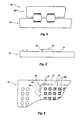
- FIG. 1is a cross-sectional representation of a first semiconductor die that may be used in assemblies and packages incorporating teachings of the present invention
- FIG. 2is a cross-sectional representation of a second semiconductor die useful in assemblies and packages incorporating teachings of the present invention
- FIG. 3is a cross-sectional representation of an assembly including the first semiconductor die shown in FIG. 1 and the second semiconductor die shown in FIG. 2 prior to the formation of electrical connections between the corresponding bond pads of the first and second semiconductor dice;
- FIG. 4is a cross-sectional representation of the assembly shown in FIG. 3 with corresponding bond pads of the first and second semiconductor dice being electrically connected to each other;
- FIG. 5is a side view of a first semiconductor die, such as that shown in FIG. 1 , with an alignment structure protruding from an active surface thereof;
- FIG. 6is a top view of the first semiconductor die and a variation of an alignment structure on an active surface of the first semiconductor die, showing use of the alignment structure to align a second semiconductor die, depicted in phantom, with the first semiconductor die;
- FIG. 7is a cross-sectional representation of a package including the assembly shown in FIG. 4 , a package body to which the assembly is electrically connected, and a package lid;
- FIG. 8is a cross-sectional representation of another embodiment of a package incorporating teachings of the present invention and including the assembly depicted in FIG. 4 , a carrier substrate to which the assembly is electrically connected, and an underfill material between at least a portion of the first semiconductor die and the adjacent portion of the carrier substrate;
- FIG. 9is a cross-sectional representation of another embodiment of a package according to the present invention, including the assembly depicted in FIG. 4 , a carrier substrate to which the assembly is electrically connected, and a glob-top type encapsulant disposed over the first semiconductor die;
- FIG. 10is a cross-sectional representation of another embodiment of a package of the present invention, which includes the assembly depicted in FIG. 4 , leads to which the assembly is electrically connected, and a molded package covering the assembly;
- FIG. 11is a cross-sectional representation of an assembly including a first semiconductor die with two second semiconductor dice flip-chip connected thereto, the first semiconductor die being flip-chip connected to a carrier substrate with conductive structures that each include a single member;
- FIG. 12is a cross-sectional representation of an assembly including a first semiconductor die with two second semiconductor dice flip-chip connected thereto, the first semiconductor die being flip-chip connected to a carrier substrate with conductive structures that each include two members;
- FIG. 13is a cross-sectional representation of an assembly including a first semiconductor die with two second semiconductor dice flip-chip connected thereto, the first semiconductor die being flip-chip connected to a carrier substrate with conductive structures that each include three members;
- FIGS. 14-16illustrate an exemplary method for fabricating a conductive mating structure to facilitate fabrication of the assembly shown in FIG. 13 ;
- FIG. 17is a cross-sectional representation of the use of the conductive mating structure depicted in FIG. 16 to form the assembly depicted in FIG. 13 .
- First semiconductor die 10that is useful in an assembly 30 (see FIG. 4 ) incorporating teachings of the present invention is illustrated.
- First semiconductor die 10includes an active surface 12 to which bond pads 14 a and 14 b (collectively referred to herein as bond pads 14 ) are exposed.
- bond pads 14are recessed relative to active surface 12 and are each laterally surrounded by an upwardly extending alignment wall 16 .
- Alignment wall 16is preferably configured to receive a conductive structure, such as a ball, bump, column, or pillar of conductive material, such as a metal, a metal alloy, a conductive epoxy, a conductor-filled epoxy, or a z-axis conductive elastomer.
- alignment walls 16are depicted as being substantially flat and extending at an angle relative to a plane of first semiconductor die 10 , shaped (i.e., curved or stepped) or textured alignment walls, as well as vertically extending alignment walls, are also within the scope of the present invention.
- bond pads 14may be substantially flush with or protrude somewhat from active surface 12 of first semiconductor die 10 .
- Outer bond pads 14 b of first semiconductor die 10may have conductive structures 17 secured thereto and protruding therefrom. Conductive structures 17 facilitate communication between first semiconductor die 10 and a carrier to which first semiconductor die 10 or an assembly including first semiconductor die 10 is electrically connected.
- Second semiconductor die 20includes bond pads 24 arranged on an active surface 22 thereof. Bond pads 24 are positioned upon active surface 22 so as to align with corresponding bond pads 14 a of first semiconductor die 10 upon orientation of second semiconductor die 20 over first semiconductor die 10 , with active surface 22 facing active surface 12 . Bond pads 24 of second semiconductor die 20 may be recessed relative to active surface 22 similarly to bond pads 14 of first semiconductor die 10 . Accordingly, bond pads 24 of second semiconductor die 20 may each be laterally surrounded by a generally upwardly extending alignment wall 26 , similar to alignment walls 16 of first semiconductor die 10 . As shown in FIG.
- each bond pad 24 of second semiconductor die 20has a conductive structure 28 secured thereto.
- the illustrated conductive structures 28are solder bumps.
- Other known types of conductive structures 28are also within the scope of the present invention, including, without limitation, balls, bumps, columns, or pillars of conductive materials such as metals, metal alloys, conductive epoxies, conductor-filled epoxies, or z-axis conductive elastomers.
- conductive structures 28may be secured to corresponding bond pads 14 a of first semiconductor die 10 .
- a second semiconductor die 20is oriented over first semiconductor die 10 with active surface 22 of second semiconductor die 20 facing active surface 12 of first semiconductor die 10 .
- bond pads 24 of second semiconductor die 20are aligned with corresponding bond pads 14 of first semiconductor die 10 , these corresponding bond pads 24 and 14 may be electrically connected to one another.
- Such alignmentmay be facilitated as alignment walls 16 of first semiconductor die 10 receive conductive structures 28 protruding from second semiconductor die 20 .
- Conductive structures 28may be electrically connected to corresponding bond pads 14 of first semiconductor die 10 as known in the art, such as by reflowing the conductive material thereof, to provide an electrically connected assembly 30 of first semiconductor die 10 and at least one second semiconductor die 20 , such as that depicted in FIG. 4 .
- first semiconductor die 10may communicate with connected semiconductor dice, such as second semiconductor die 20 , at much faster rates than are possible with conventional multi-chip modules.
- first semiconductor die 10may have an alignment structure 18 secured to active surface 12 thereof.
- Alignment structure 18is preferably configured to guide at least two adjoined peripheral edges of another semiconductor die during orientation thereof upon active surface 12 of first semiconductor die 10 .
- FIG. 6illustrates the use of alignment structure 18 to properly align bond pads 24 of a second semiconductor die 20 ( FIG. 2 ) relative to corresponding bond pads 14 a of first semiconductor die 10 upon orientation of second semiconductor die 20 over first semiconductor die 10 with active surface 22 facing active surface 12 .
- alignment structure 18includes two members 19 . Alignment structures 18 , however, with other numbers or configurations of members 19 that are configured to guide two or more adjoining peripheral edges 21 of second semiconductor die 20 are also within the scope of the present invention.
- Each member 19 of alignment structure 18may be fabricated by known processes.
- members 19 of alignment structure 18may be fabricated directly upon active surface 12 of first semiconductor die 10 by forming a material layer, such as a layer of glass, silicon dioxide, or silicon nitride by known processes, on active surface 12 and patterning the material layer, also by known processes.
- a photoimageable materialsuch as a photoresist or a polyimide, may be disposed on active surface 12 of first semiconductor die 10 and patterned by known photoimaging processes.
- members 19 thereofmay be formed by known stereolithography techniques, such as that disclosed in U.S. patent application Ser. No. 09/259,142, filed on Feb.
- one or more layers of substantially unconsolidated materialsuch as a photoimageable polymer, or “photopolymer,” may be formed and at least partially selectively consolidated. If member 19 includes a plurality of layers, the layers are at least partially superimposed over one another, contiguous with one another, and mutually adhered to each other.
- stereolithographymay be used to fabricate alignment structures 18 directly on active surface 12 or separately from first semiconductor die 10 , in which case each member 19 of alignment structure 18 may subsequently be secured to active surface 12 as known in the art, such as by use of an appropriate adhesive material.
- FIGS. 7-10illustrate exemplary packages that include an assembly 30 of a first semiconductor die 10 and a second semiconductor die 20 .
- a package 40includes assembly 30 , a package body 41 , which is also referred to herein as a carrier substrate, configured to receive assembly 30 and to be electrically connected thereto, and a package lid 50 configured to be assembled with package body 41 so as to enclose assembly 30 within package 40 .
- package body 41includes a recessed surface 42 laterally bounded by upwardly extending peripheral walls 43 .
- Peripheral walls 43define a receptacle 44 configured to receive assembly 30 .
- Surface 42carries contact pads 45 that are arranged thereon so as to align with corresponding outer bond pads 14 b of first semiconductor die 10 upon introduction of assembly 30 into receptacle 44 with active surface 12 of first semiconductor die 10 facing surface 42 of package body 41 .
- Contact pads 45are electrically connected to conductive traces 46 that are carried by package body 41 and, in turn, electrically connected to terminals or other connective elements (not shown) that facilitate communication between semiconductor dice 10 , 20 of package 40 and external components (not shown).
- conductive structures 17may be secured to corresponding contact pads 45 of package body 41 , rather than to outer bond pads 14 b of first semiconductor die 10 .
- package body 41also includes a die receptacle 47 recessed in surface 42 .
- Die receptacle 47is located and configured to at least partially receive a second semiconductor die 20 of assembly 30 .
- Each die receptacle 47may include therein a quantity of thermal grease 48 of a known type to facilitate the transfer of heat away from second semiconductor die 20 during operation thereof.
- Thermal grease 48may also be used to secure second semiconductor die 20 or assembly 30 to a carrier, such as package body 41 , prior to the bonding of outer bond pads 14 b to their corresponding contact pads 45 with conductive structures 17 .
- conductive structures 28may protrude from active surface 22 of second semiconductor die 20 substantially the same distance that conductive structures 17 protrude from active surface 12 of first semiconductor die 10 .
- the distance that conductive structures 17 protrude from active surface 12 of first semiconductor die 10is preferably sufficient to permit conductive structures 17 to contact corresponding contact pads 45 upon orientation of first semiconductor die 10 invertedly over package body 41 or another carrier.
- assembly 30may be electrically connected to package body 41 by reflowing conductive structures 17 protruding from outer bond pads 14 b to secure conductive structures to contact pads 45 corresponding to outer bond pads 14 b , or as otherwise known in the art.
- lid 50may be disposed over receptacle 44 so as to enclose assembly 30 within package 40 .
- Lid 50may be secured to package body 41 as known in the art, such as by use of adhesives or mechanically.
- An alternative method for electrically connecting assembly 30 to package body 41includes orienting a second semiconductor die 20 in each die receptacle 47 of package body 41 with active surface 22 facing into receptacle 44 .
- a first semiconductor die 10is invertedly oriented within receptacle 44 with active surface 12 thereof facing surface 42 of package body 41 and active surface 22 of second semiconductor die 20 .
- bond pads 24 and corresponding bond pads 14 aare aligned.
- Conductive structures 17 and 28may then be connected between bond pads 24 and corresponding bond pads 14 a and between outer bond pads 14 b and corresponding contact pads 45 as known in the art, such as by reflowing the conductive materials of conductive structures 17 and 28 . In this manner, electrical connections between first and second semiconductor dice 10 and 20 , as well as between assembly 30 and package body 41 , may be substantially simultaneously formed.
- Package 40 ′includes a substantially planar carrier substrate 60 .
- Carrier substrate 60includes a surface 62 upon which contact pads 64 are carried.
- Conductive traces 66 that communicate with corresponding contact pads 64are also carried by carrier substrate 60 and lead to external conductive elements (not shown) to facilitate communication between an assembly 30 electrically connected to carrier substrate 60 and external components (not shown).
- Carrier substrate 60may also include at least one receptacle 70 recessed in surface 62 .
- Each receptacle 70is preferably located and configured so as to at least partially receive a second semiconductor die 20 of an assembly 30 upon orientation of assembly 30 over carrier substrate 60 with active surface 12 of first semiconductor die 10 facing surface 62 of carrier substrate 60 .
- Assembly 30may be electrically connected and secured to carrier substrate 60 by known processes, such as those disclosed with reference to the connection of assembly 30 to package body 41 illustrated in FIG. 7 .
- Package 40 ′also includes a quantity of underfill material 72 of a known type between active surface 12 of first semiconductor die 10 and surface 62 of carrier substrate 60 .
- FIG. 9illustrates another embodiment of package 40 ′′, which includes a substantially planar carrier substrate 60 with an assembly 30 of a first semiconductor die 10 and second semiconductor die 20 electrically connected and secured thereto.
- Package 40 ′′also includes a quantity of encapsulant material 74 disposed over first semiconductor die 10 and in contact with surface 62 of carrier substrate 60 so as to encapsulate and seal assembly 30 .
- encapsulant material 74is a conventional “glob-top” type encapsulant, such as silicone or an epoxy.
- FIG. 10Yet another embodiment of a package 40 ′ 41 according to the present invention is illustrated in FIG. 10 .
- Package 40 ′ 41includes assembly 30 electrically connected to a carrier comprising leads 80 , such as in the illustrated leads-over-chip (LOC) arrangement.
- Package 40 ′′′includes a molded encapsulant 82 substantially covering and encapsulating assembly 30 .
- Molded encapsulant 82may be fabricated from known materials, such as thermoset resins (including particle-filled resins), and by known techniques, such as transfer molding processes.
- conductive structures 17 , 28are preferably formed from a conductive material that will survive the transfer molding process, such as a conductive epoxy or a conductor-filled epoxy.
- FIGS. 11-13depict alternative types of conductive structures that may be used in accordance with teachings of the present invention.
- FIG. 11illustrates an assembly 130 that includes one first semiconductor die 110 and two second semiconductor dice 120 flip-chip connected thereto by way of conductive structures 128 , such as solder balls.
- Assembly 130also includes a carrier substrate 160 upon which second semiconductor dice 120 rest and to which first semiconductor die 110 is electrically connected.
- each second semiconductor die 120rests upon a layer of thermal grease 163 of thickness L disposed on a surface 162 of carrier substrate 160 .
- Each second semiconductor die 120has a thickness T.
- Each conductive structure 128extends a distance D between a plane of active surface 122 of second semiconductor die 120 and a plane of active surface 112 of first semiconductor die 110 .
- active surface 112 of first semiconductor die 110is separated from surface 162 of carrier substrate 160 by a distance of about L+T+D.
- conductive structures 117 extending between corresponding outer bond pads 114 b and contact pads 164preferably have a height of about L+T+D.
- a variation of an assembly 130 ′ incorporating teachings of the present invention, shown in FIG. 12includes the same elements as assembly 130 , shown in FIG. 11 , except for conductive structures 117 . Rather, assembly 130 ′ includes conductive structures 117 ′ that include two members 117 a′ and 117 b′ . Members 117 a′ may be predisposed on outer bond pads 114 b of first semiconductor die 110 , while members 117 b′ may be predisposed on contact pads 164 of carrier substrate 160 . The collective distances that members 117 a′ and 117 b′ protrude from active surface 112 and surface 162 , respectively, are about equal to L+T+D.
- first semiconductor die 110is invertedly oriented and aligned over carrier substrate 160 , members 117 a ′ and 117 b′ of each conductive structure 117 ′ are aligned and abut one another.
- integral conductive structures 117 ′that electrically connect corresponding outer bond pads 114 b and contact pads 164 to each other are formed.
- FIG. 13depicts another variation of an assembly 130 ′′ according to the present invention, which again includes the same elements as assembly 130 , shown in FIG. 11 , with the exception of conductive structures 117 .
- assembly 130 ′′includes conductive structures 117 ′′ with more than two members, 117 a′′ , 117 b′′ , 117 c′′ , etc.
- Members 117 a′′ and 117 c′′may comprise conductive structures that are predisposed on outer bond pads 114 b and their corresponding contact pads 164 , respectively.
- Members 117 b′′may be formed by the process illustrated in FIGS. 14-17 , or as otherwise known in the art.
- a layer 214 of an electrically insulative support materialsuch as a polymer (e.g., a polyimide), is applied to a surface 213 of a substantially planar conductive layer 212 including a conductive material that will adhere to the conductive materials of members 117 a′′ and 117 c′′ ( FIG. 13 ) during reflow of the conductive materials or otherwise, as known in the art.
- Polymeric layer 214may be applied to conductive layer 212 by known processes, such as by spray-on techniques, spin-on techniques, or by other techniques for forming layers from polymeric materials.
- Conductive layer 212may include a single layer of conductive material or more than one sublayer of conductive material.
- conductive layer 212is patterned to form members 117 b′′ in desired locations on polymeric layer 214 .
- Members 117 b′′are each preferably sized and positioned so as to facilitate alignment thereof with corresponding members 117 a′′ and 117 c′′ (FIG. 13 ).
- Conductive layer 212may be patterned as known in the art, such as by use of photomask and etch processes.
- a layer 216 of an electrically insulative support materialsuch as a polymer (e.g., polyimide or polyester, such as the polyester film marketed by E. I. du Pont De Nemours and Company of Wilmington, Del. as MYLAR®) or other material that may be removed without damaging conductive structures 117 ′′ ( FIG.
- each member 117 b′′may then be disposed laterally adjacent at least a portion of each member 117 b′′ so as to support same upon removal of polymeric layer 214 therefrom.
- Members 117 b′′ and layers 214 and 216collectively form a conductive mating structure 210 .
- the structure 210 shown in FIG. 15may also be fabricated by disposing preformed members 117 b′′ on a layer 214 of an electrically nonconductive polymeric material, with members 117 b′′ being secured to polymeric layer 214 by adhesion of the material thereof or with a separate adhesive material. Layer 216 may then be formed as described above.
- polymeric layer 214is at least partially removed so as to at least partially expose ends 118 of members 117 b′′ . Ends 218 of layers 214 and 216 that are alignable with second semiconductor dice 120 upon assembly are also removed so as to form through structure 210 slots 220 configured to receive second semiconductor dice 120 (FIG. 17 ).
- carrier substrate 160 and the assembly of first and second semiconductor dice 110 , 120are assembled with structure 210 disposed therebetween.
- corresponding members 117 a′′ , 117 b′′ , and 117 c′′ of each conductive structure 117 ′′are in substantial alignment and second semiconductor dice 120 are received by corresponding slots 220 .
- Corresponding members 117 a′′ , 117 b′′ , and 117 c′′may be secured so as to electrically communicate with one another by known processes, such as by reflowing the conductive material or materials thereof.
- the remainders of layers 214 ( FIG. 16 ) and 216may then be removed from assembly 130 ′′ or remain therein.
Landscapes
- Engineering & Computer Science (AREA)
- Microelectronics & Electronic Packaging (AREA)
- Power Engineering (AREA)
- Physics & Mathematics (AREA)
- Condensed Matter Physics & Semiconductors (AREA)
- General Physics & Mathematics (AREA)
- Computer Hardware Design (AREA)
- Manufacturing & Machinery (AREA)
- Wire Bonding (AREA)
Abstract
Description
Claims (46)
Priority Applications (1)
| Application Number | Priority Date | Filing Date | Title |
|---|---|---|---|
| US10/382,025US6906408B2 (en) | 2000-07-12 | 2003-03-05 | Assemblies and packages including die-to-die connections |
Applications Claiming Priority (3)
| Application Number | Priority Date | Filing Date | Title |
|---|---|---|---|
| US09/615,009US6525413B1 (en) | 2000-07-12 | 2000-07-12 | Die to die connection method and assemblies and packages including dice so connected |
| US09/944,487US6984544B2 (en) | 2000-07-12 | 2001-08-30 | Die to die connection method and assemblies and packages including dice so connected |
| US10/382,025US6906408B2 (en) | 2000-07-12 | 2003-03-05 | Assemblies and packages including die-to-die connections |
Related Parent Applications (1)
| Application Number | Title | Priority Date | Filing Date |
|---|---|---|---|
| US09/944,487ContinuationUS6984544B2 (en) | 2000-07-12 | 2001-08-30 | Die to die connection method and assemblies and packages including dice so connected |
Publications (2)
| Publication Number | Publication Date |
|---|---|
| US20030160321A1 US20030160321A1 (en) | 2003-08-28 |
| US6906408B2true US6906408B2 (en) | 2005-06-14 |
Family
ID=24463622
Family Applications (4)
| Application Number | Title | Priority Date | Filing Date |
|---|---|---|---|
| US09/615,009Expired - LifetimeUS6525413B1 (en) | 2000-07-12 | 2000-07-12 | Die to die connection method and assemblies and packages including dice so connected |
| US09/944,487Expired - Fee RelatedUS6984544B2 (en) | 2000-07-12 | 2001-08-30 | Die to die connection method and assemblies and packages including dice so connected |
| US10/382,025Expired - LifetimeUS6906408B2 (en) | 2000-07-12 | 2003-03-05 | Assemblies and packages including die-to-die connections |
| US11/325,294AbandonedUS20060115929A1 (en) | 2000-07-12 | 2006-01-04 | Die-to-die connection method and assemblies and packages including dice so connected |
Family Applications Before (2)
| Application Number | Title | Priority Date | Filing Date |
|---|---|---|---|
| US09/615,009Expired - LifetimeUS6525413B1 (en) | 2000-07-12 | 2000-07-12 | Die to die connection method and assemblies and packages including dice so connected |
| US09/944,487Expired - Fee RelatedUS6984544B2 (en) | 2000-07-12 | 2001-08-30 | Die to die connection method and assemblies and packages including dice so connected |
Family Applications After (1)
| Application Number | Title | Priority Date | Filing Date |
|---|---|---|---|
| US11/325,294AbandonedUS20060115929A1 (en) | 2000-07-12 | 2006-01-04 | Die-to-die connection method and assemblies and packages including dice so connected |
Country Status (1)
| Country | Link |
|---|---|
| US (4) | US6525413B1 (en) |
Cited By (34)
| Publication number | Priority date | Publication date | Assignee | Title |
|---|---|---|---|---|
| US20030148597A1 (en)* | 2002-01-09 | 2003-08-07 | Tan Hock Chuan | Stacked die in die BGA package |
| US20040227240A1 (en)* | 2003-05-12 | 2004-11-18 | Bolken Todd O. | Semiconductor component having encapsulated die stack |
| US20060038272A1 (en)* | 2004-08-17 | 2006-02-23 | Texas Instruments Incorporated | Stacked wafer scale package |
| US20060163722A1 (en)* | 2005-01-21 | 2006-07-27 | Phoenix Precision Technology Corporation | Semiconductor chip electrical connection structure |
| US20090014860A1 (en)* | 2007-07-13 | 2009-01-15 | Siliconware Precision Industries Co., Ltd. | Multi-chip stack structure and fabricating method thereof |
| CN100505196C (en)* | 2005-11-25 | 2009-06-24 | 全懋精密科技股份有限公司 | Chip electrical connection structure and manufacturing method thereof |
| US20100244276A1 (en)* | 2009-03-25 | 2010-09-30 | Lsi Corporation | Three-dimensional electronics package |
| US8084297B1 (en)* | 2006-01-27 | 2011-12-27 | Xilinx, Inc. | Method of implementing a capacitor in an integrated circuit |
| US20170103968A1 (en)* | 2015-10-12 | 2017-04-13 | Invensas Corporation | Embedded wire bond wires |
| US20170170105A1 (en)* | 2015-12-15 | 2017-06-15 | Intel Corporation | Integrated circuit package structures |
| US9812402B2 (en) | 2015-10-12 | 2017-11-07 | Invensas Corporation | Wire bond wires for interference shielding |
| US9842745B2 (en) | 2012-02-17 | 2017-12-12 | Invensas Corporation | Heat spreading substrate with embedded interconnects |
| US9852969B2 (en) | 2013-11-22 | 2017-12-26 | Invensas Corporation | Die stacks with one or more bond via arrays of wire bond wires and with one or more arrays of bump interconnects |
| US9888579B2 (en) | 2015-03-05 | 2018-02-06 | Invensas Corporation | Pressing of wire bond wire tips to provide bent-over tips |
| US9911718B2 (en) | 2015-11-17 | 2018-03-06 | Invensas Corporation | ‘RDL-First’ packaged microelectronic device for a package-on-package device |
| US9935075B2 (en) | 2016-07-29 | 2018-04-03 | Invensas Corporation | Wire bonding method and apparatus for electromagnetic interference shielding |
| US9953914B2 (en) | 2012-05-22 | 2018-04-24 | Invensas Corporation | Substrate-less stackable package with wire-bond interconnect |
| US9984992B2 (en) | 2015-12-30 | 2018-05-29 | Invensas Corporation | Embedded wire bond wires for vertical integration with separate surface mount and wire bond mounting surfaces |
| US10008477B2 (en) | 2013-09-16 | 2018-06-26 | Invensas Corporation | Microelectronic element with bond elements to encapsulation surface |
| US10008469B2 (en) | 2015-04-30 | 2018-06-26 | Invensas Corporation | Wafer-level packaging using wire bond wires in place of a redistribution layer |
| US10026717B2 (en) | 2013-11-22 | 2018-07-17 | Invensas Corporation | Multiple bond via arrays of different wire heights on a same substrate |
| US10062661B2 (en) | 2011-05-03 | 2018-08-28 | Tessera, Inc. | Package-on-package assembly with wire bonds to encapsulation surface |
| US10121768B2 (en) | 2015-05-27 | 2018-11-06 | Bridge Semiconductor Corporation | Thermally enhanced face-to-face semiconductor assembly with built-in heat spreader and method of making the same |
| US10128216B2 (en) | 2010-07-19 | 2018-11-13 | Tessera, Inc. | Stackable molded microelectronic packages |
| US10181457B2 (en) | 2015-10-26 | 2019-01-15 | Invensas Corporation | Microelectronic package for wafer-level chip scale packaging with fan-out |
| US10297582B2 (en) | 2012-08-03 | 2019-05-21 | Invensas Corporation | BVA interposer |
| US10299368B2 (en) | 2016-12-21 | 2019-05-21 | Invensas Corporation | Surface integrated waveguides and circuit structures therefor |
| US10332854B2 (en) | 2015-10-23 | 2019-06-25 | Invensas Corporation | Anchoring structure of fine pitch bva |
| US10354984B2 (en) | 2015-05-27 | 2019-07-16 | Bridge Semiconductor Corporation | Semiconductor assembly with electromagnetic shielding and thermally enhanced characteristics and method of making the same |
| US10381326B2 (en) | 2014-05-28 | 2019-08-13 | Invensas Corporation | Structure and method for integrated circuits packaging with increased density |
| US10460958B2 (en) | 2013-08-07 | 2019-10-29 | Invensas Corporation | Method of manufacturing embedded packaging with preformed vias |
| US10529636B2 (en) | 2014-01-17 | 2020-01-07 | Invensas Corporation | Fine pitch BVA using reconstituted wafer with area array accessible for testing |
| US10756049B2 (en) | 2011-10-17 | 2020-08-25 | Invensas Corporation | Package-on-package assembly with wire bond vias |
| US11291146B2 (en) | 2014-03-07 | 2022-03-29 | Bridge Semiconductor Corp. | Leadframe substrate having modulator and crack inhibiting structure and flip chip assembly using the same |
Families Citing this family (95)
| Publication number | Priority date | Publication date | Assignee | Title |
|---|---|---|---|---|
| KR100246366B1 (en)* | 1997-12-04 | 2000-03-15 | 김영환 | Area array type semiconductor package and fabrication method of the same |
| US6524346B1 (en)* | 1999-02-26 | 2003-02-25 | Micron Technology, Inc. | Stereolithographic method for applying materials to electronic component substrates and resulting structures |
| EP1189280A4 (en)* | 2000-03-29 | 2005-03-02 | Rohm Co Ltd | Semiconductor device |
| US7774219B1 (en) | 2000-04-28 | 2010-08-10 | Microsoft Corporation | Long running transaction integration with selective dehydration and selective compensation |
| US6525413B1 (en)* | 2000-07-12 | 2003-02-25 | Micron Technology, Inc. | Die to die connection method and assemblies and packages including dice so connected |
| JP2002270762A (en)* | 2001-03-09 | 2002-09-20 | Sony Corp | Semiconductor device |
| WO2002082540A1 (en)* | 2001-03-30 | 2002-10-17 | Fujitsu Limited | Semiconductor device, method of manufacture thereof, and semiconductor substrate |
| DE10120917C1 (en)* | 2001-04-27 | 2002-11-28 | Infineon Technologies Ag | Arrangement with at least two centered stacked semiconductor chips |
| US20030048624A1 (en)* | 2001-08-22 | 2003-03-13 | Tessera, Inc. | Low-height multi-component assemblies |
| US6674647B2 (en)* | 2002-01-07 | 2004-01-06 | International Business Machines Corporation | Low or no-force bump flattening structure and method |
| US6867500B2 (en)* | 2002-04-08 | 2005-03-15 | Micron Technology, Inc. | Multi-chip module and methods |
| SG127684A1 (en)* | 2002-08-19 | 2006-12-29 | Micron Technology Inc | Packaged microelectronic component assemblies |
| US7253510B2 (en) | 2003-01-16 | 2007-08-07 | International Business Machines Corporation | Ball grid array package construction with raised solder ball pads |
| US20040262368A1 (en)* | 2003-06-26 | 2004-12-30 | Haw Tan Tzyy | Ball grid array solder joint reliability |
| KR20050001159A (en)* | 2003-06-27 | 2005-01-06 | 삼성전자주식회사 | Multi-chip package having a plurality of flip chips and fabrication method thereof |
| WO2005001933A2 (en)* | 2003-06-28 | 2005-01-06 | Infineon Technologies Ag | Multichip semi-conductor component and method for the production thereof |
| TWI313048B (en)* | 2003-07-24 | 2009-08-01 | Via Tech Inc | Multi-chip package |
| US8269329B2 (en)* | 2003-07-24 | 2012-09-18 | Via Technologies, Inc. | Multi-chip package |
| US7203387B2 (en)* | 2003-09-10 | 2007-04-10 | Agency For Science, Technology And Research | VLSI-photonic heterogeneous integration by wafer bonding |
| US20050104171A1 (en)* | 2003-11-13 | 2005-05-19 | Benson Peter A. | Microelectronic devices having conductive complementary structures and methods of manufacturing microelectronic devices having conductive complementary structures |
| US7525199B1 (en)* | 2004-05-21 | 2009-04-28 | Sun Microsystems, Inc | Packaging for proximity communication positioned integrated circuits |
| US20060027899A1 (en)* | 2004-06-25 | 2006-02-09 | Tessera, Inc. | Structure with spherical contact pins |
| US7553680B2 (en)* | 2004-08-09 | 2009-06-30 | Delphi Technologies, Inc. | Methods to provide and expose a diagnostic connector on overmolded electronic packages |
| US7454105B2 (en)* | 2004-11-22 | 2008-11-18 | Avago Technologies Fiber Ip (Singapore) Pte. Ltd. | Passive alignment using elastic averaging in optoelectronics applications |
| KR100650732B1 (en) | 2004-12-28 | 2006-11-27 | 주식회사 하이닉스반도체 | stacked chip package |
| US7230333B2 (en) | 2005-04-21 | 2007-06-12 | International Rectifier Corporation | Semiconductor package |
| US20060261498A1 (en)* | 2005-05-17 | 2006-11-23 | Micron Technology, Inc. | Methods and apparatuses for encapsulating microelectronic devices |
| US7671478B2 (en)* | 2005-09-02 | 2010-03-02 | Honeywell International Inc. | Low height vertical sensor packaging |
| US7576995B2 (en)* | 2005-11-04 | 2009-08-18 | Entorian Technologies, Lp | Flex circuit apparatus and method for adding capacitance while conserving circuit board surface area |
| US8067267B2 (en)* | 2005-12-23 | 2011-11-29 | Tessera, Inc. | Microelectronic assemblies having very fine pitch stacking |
| US7508058B2 (en)* | 2006-01-11 | 2009-03-24 | Entorian Technologies, Lp | Stacked integrated circuit module |
| US7304382B2 (en) | 2006-01-11 | 2007-12-04 | Staktek Group L.P. | Managed memory component |
| US7605454B2 (en) | 2006-01-11 | 2009-10-20 | Entorian Technologies, Lp | Memory card and method for devising |
| US7608920B2 (en)* | 2006-01-11 | 2009-10-27 | Entorian Technologies, Lp | Memory card and method for devising |
| US7508069B2 (en) | 2006-01-11 | 2009-03-24 | Entorian Technologies, Lp | Managed memory component |
| US20070158821A1 (en)* | 2006-01-11 | 2007-07-12 | Leland Szewerenko | Managed memory component |
| US20070164416A1 (en)* | 2006-01-17 | 2007-07-19 | James Douglas Wehrly | Managed memory component |
| US7663232B2 (en)* | 2006-03-07 | 2010-02-16 | Micron Technology, Inc. | Elongated fasteners for securing together electronic components and substrates, semiconductor device assemblies including such fasteners, and accompanying systems |
| US7682869B2 (en)* | 2006-03-23 | 2010-03-23 | Micron Technology, Inc. | Method of packaging integrated circuit devices using preformed carrier |
| US20070262429A1 (en)* | 2006-05-15 | 2007-11-15 | Staktek Group, L.P. | Perimeter stacking system and method |
| US9299634B2 (en)* | 2006-05-16 | 2016-03-29 | Broadcom Corporation | Method and apparatus for cooling semiconductor device hot blocks and large scale integrated circuit (IC) using integrated interposer for IC packages |
| US9013035B2 (en)* | 2006-06-20 | 2015-04-21 | Broadcom Corporation | Thermal improvement for hotspots on dies in integrated circuit packages |
| US7468553B2 (en)* | 2006-10-20 | 2008-12-23 | Entorian Technologies, Lp | Stackable micropackages and stacked modules |
| US20080164605A1 (en)* | 2007-01-08 | 2008-07-10 | United Microelectronics Corp. | Multi-chip package |
| US7833456B2 (en)* | 2007-02-23 | 2010-11-16 | Micron Technology, Inc. | Systems and methods for compressing an encapsulant adjacent a semiconductor workpiece |
| SG147330A1 (en) | 2007-04-19 | 2008-11-28 | Micron Technology Inc | Semiconductor workpiece carriers and methods for processing semiconductor workpieces |
| US8723332B2 (en)* | 2007-06-11 | 2014-05-13 | Invensas Corporation | Electrically interconnected stacked die assemblies |
| US8367471B2 (en) | 2007-06-15 | 2013-02-05 | Micron Technology, Inc. | Semiconductor assemblies, stacked semiconductor devices, and methods of manufacturing semiconductor assemblies and stacked semiconductor devices |
| TW200917391A (en)* | 2007-06-20 | 2009-04-16 | Vertical Circuits Inc | Three-dimensional circuitry formed on integrated circuit device using two-dimensional fabrication |
| US7799608B2 (en)* | 2007-08-01 | 2010-09-21 | Advanced Micro Devices, Inc. | Die stacking apparatus and method |
| WO2009035849A2 (en) | 2007-09-10 | 2009-03-19 | Vertical Circuits, Inc. | Semiconductor die mount by conformal die coating |
| US8487428B2 (en)* | 2007-11-20 | 2013-07-16 | Fujitsu Limited | Method and system for providing a reliable semiconductor assembly |
| JP5425404B2 (en)* | 2008-01-18 | 2014-02-26 | 東京エレクトロン株式会社 | Method for processing amorphous carbon film and method for manufacturing semiconductor device using the same |
| US20090184416A1 (en)* | 2008-01-22 | 2009-07-23 | Yinon Degani | MCM packages |
| CN101999167B (en)* | 2008-03-12 | 2013-07-17 | 伊文萨思公司 | Support mounted electrically interconnected die assembly |
| US7863159B2 (en)* | 2008-06-19 | 2011-01-04 | Vertical Circuits, Inc. | Semiconductor die separation method |
| US9153517B2 (en) | 2008-05-20 | 2015-10-06 | Invensas Corporation | Electrical connector between die pad and z-interconnect for stacked die assemblies |
| US8420722B2 (en)* | 2008-07-10 | 2013-04-16 | Electronics And Telecommunications Research Institute | Composition and methods of forming solder bump and flip chip using the same |
| US20100102457A1 (en)* | 2008-10-28 | 2010-04-29 | Topacio Roden R | Hybrid Semiconductor Chip Package |
| US7979813B2 (en)* | 2009-01-15 | 2011-07-12 | Micrel, Inc. | Chip-scale package conversion technique for dies |
| WO2010151578A2 (en)* | 2009-06-26 | 2010-12-29 | Vertical Circuits, Inc. | Electrical interconnect for die stacked in zig-zag configuration |
| WO2011056668A2 (en) | 2009-10-27 | 2011-05-12 | Vertical Circuits, Inc. | Selective die electrical insulation additive process |
| TWI544604B (en) | 2009-11-04 | 2016-08-01 | 英維瑟斯公司 | Stacked die assembly having reduced stress electrical interconnects |
| US8198131B2 (en)* | 2009-11-18 | 2012-06-12 | Advanced Semiconductor Engineering, Inc. | Stackable semiconductor device packages |
| US8299633B2 (en) | 2009-12-21 | 2012-10-30 | Advanced Micro Devices, Inc. | Semiconductor chip device with solder diffusion protection |
| TWI408785B (en)* | 2009-12-31 | 2013-09-11 | Advanced Semiconductor Eng | Semiconductor package |
| US8569894B2 (en) | 2010-01-13 | 2013-10-29 | Advanced Semiconductor Engineering, Inc. | Semiconductor package with single sided substrate design and manufacturing methods thereof |
| US20110175218A1 (en)* | 2010-01-18 | 2011-07-21 | Shiann-Ming Liou | Package assembly having a semiconductor substrate |
| US20130026609A1 (en)* | 2010-01-18 | 2013-01-31 | Marvell World Trade Ltd. | Package assembly including a semiconductor substrate with stress relief structure |
| US20110186960A1 (en) | 2010-02-03 | 2011-08-04 | Albert Wu | Techniques and configurations for recessed semiconductor substrates |
| TWI419283B (en) | 2010-02-10 | 2013-12-11 | Advanced Semiconductor Eng | Package structure |
| TWI411075B (en) | 2010-03-22 | 2013-10-01 | Advanced Semiconductor Eng | Semiconductor package and manufacturing method thereof |
| US8278746B2 (en) | 2010-04-02 | 2012-10-02 | Advanced Semiconductor Engineering, Inc. | Semiconductor device packages including connecting elements |
| US8624374B2 (en) | 2010-04-02 | 2014-01-07 | Advanced Semiconductor Engineering, Inc. | Semiconductor device packages with fan-out and with connecting elements for stacking and manufacturing methods thereof |
| TWI451546B (en) | 2010-10-29 | 2014-09-01 | Advanced Semiconductor Eng | Stacked semiconductor package, semiconductor package thereof and method for making a semiconductor package |
| US20120193788A1 (en) | 2011-01-31 | 2012-08-02 | Advanced Micro Devices, Inc. | Stacked semiconductor chips packaging |
| US9171792B2 (en) | 2011-02-28 | 2015-10-27 | Advanced Semiconductor Engineering, Inc. | Semiconductor device packages having a side-by-side device arrangement and stacking functionality |
| US8580594B2 (en) | 2011-08-09 | 2013-11-12 | Taiwan Semiconductor Manufacturing Company, Ltd. | Method of fabricating a semiconductor device having recessed bonding site |
| WO2013095546A1 (en)* | 2011-12-22 | 2013-06-27 | Intel Corporation | 3d integrated circuit package with through-mold first level interconnects |
| US20150380392A1 (en)* | 2014-06-27 | 2015-12-31 | Apple Inc. | Package with memory die and logic die interconnected in a face-to-face configuration |
| US9356001B2 (en) | 2014-10-02 | 2016-05-31 | HGST Netherlands B.V. | Semiconductor device with at least one voltage-guided conductive filament |
| US10515884B2 (en)* | 2015-02-17 | 2019-12-24 | Advanced Semiconductor Engineering, Inc. | Substrate having a conductive structure within photo-sensitive resin |
| US20160240457A1 (en)* | 2015-02-18 | 2016-08-18 | Altera Corporation | Integrated circuit packages with dual-sided stacking structure |
| US9490195B1 (en) | 2015-07-17 | 2016-11-08 | Invensas Corporation | Wafer-level flipped die stacks with leadframes or metal foil interconnects |
| US9825002B2 (en) | 2015-07-17 | 2017-11-21 | Invensas Corporation | Flipped die stack |
| US9871019B2 (en) | 2015-07-17 | 2018-01-16 | Invensas Corporation | Flipped die stack assemblies with leadframe interconnects |
| US9508691B1 (en) | 2015-12-16 | 2016-11-29 | Invensas Corporation | Flipped die stacks with multiple rows of leadframe interconnects |
| US10566310B2 (en) | 2016-04-11 | 2020-02-18 | Invensas Corporation | Microelectronic packages having stacked die and wire bond interconnects |
| KR102609714B1 (en)* | 2016-04-27 | 2023-12-05 | 엘지전자 주식회사 | Sensor |
| US9595511B1 (en) | 2016-05-12 | 2017-03-14 | Invensas Corporation | Microelectronic packages and assemblies with improved flyby signaling operation |
| US9728524B1 (en) | 2016-06-30 | 2017-08-08 | Invensas Corporation | Enhanced density assembly having microelectronic packages mounted at substantial angle to board |
| US10510721B2 (en) | 2017-08-11 | 2019-12-17 | Advanced Micro Devices, Inc. | Molded chip combination |
| US10593628B2 (en) | 2018-04-24 | 2020-03-17 | Advanced Micro Devices, Inc. | Molded die last chip combination |
| US10672712B2 (en) | 2018-07-30 | 2020-06-02 | Advanced Micro Devices, Inc. | Multi-RDL structure packages and methods of fabricating the same |
| US10923430B2 (en) | 2019-06-30 | 2021-02-16 | Advanced Micro Devices, Inc. | High density cross link die with polymer routing layer |
Citations (44)
| Publication number | Priority date | Publication date | Assignee | Title |
|---|---|---|---|---|
| US3777221A (en) | 1972-12-18 | 1973-12-04 | Ibm | Multi-layer circuit package |
| US5014161A (en) | 1985-07-22 | 1991-05-07 | Digital Equipment Corporation | System for detachably mounting semiconductors on conductor substrate |
| JPH04243173A (en) | 1991-01-17 | 1992-08-31 | Nec Corp | electrostrictive effect element |
| JPH05151617A (en) | 1991-11-29 | 1993-06-18 | Matsushita Electric Ind Co Ltd | Optical information recording medium and manufacture thereof |
| US5291061A (en) | 1993-04-06 | 1994-03-01 | Micron Semiconductor, Inc. | Multi-chip stacked devices |
| US5302778A (en) | 1992-08-28 | 1994-04-12 | Eastman Kodak Company | Semiconductor insulation for optical devices |
| US5435734A (en) | 1991-10-09 | 1995-07-25 | Chow; Vincent | Direct integrated circuit interconnector system |
| USRE35119E (en) | 1988-07-21 | 1995-12-12 | At&T Corp. | Textured metallic compression bonding |
| US5477082A (en) | 1994-01-11 | 1995-12-19 | Exponential Technology, Inc. | Bi-planar multi-chip module |
| US5477086A (en) | 1993-04-30 | 1995-12-19 | Lsi Logic Corporation | Shaped, self-aligning micro-bump structures |
| US5532519A (en) | 1994-09-14 | 1996-07-02 | International Business Machines Corporation | Cube wireability enhancement with chip-to-chip alignment and thickness control |
| US5535101A (en)* | 1992-11-03 | 1996-07-09 | Motorola, Inc. | Leadless integrated circuit package |
| US5559444A (en) | 1991-06-04 | 1996-09-24 | Micron Technology, Inc. | Method and apparatus for testing unpackaged semiconductor dice |
| US5561328A (en) | 1991-06-24 | 1996-10-01 | Digital Equipment Corporation | Photo-definable template for semiconductor chip alignment |
| US5719436A (en) | 1995-03-13 | 1998-02-17 | Intel Corporation | Package housing multiple semiconductor dies |
| US5767580A (en) | 1993-04-30 | 1998-06-16 | Lsi Logic Corporation | Systems having shaped, self-aligning micro-bump structures |
| US5773320A (en) | 1995-11-13 | 1998-06-30 | Asea Brown Boveri Ag | Method for producing a power semiconductor module |
| US5777345A (en) | 1996-01-03 | 1998-07-07 | Intel Corporation | Multi-chip integrated circuit package |
| US5790839A (en) | 1996-12-20 | 1998-08-04 | International Business Machines Corporation | System integration of DRAM macros and logic cores in a single chip architecture |
| US5883814A (en) | 1997-03-13 | 1999-03-16 | International Business Machines Corporation | System-on-chip layout compilation |
| US5900676A (en) | 1996-08-19 | 1999-05-04 | Samsung Electronics Co., Ltd. | Semiconductor device package structure having column leads and a method for production thereof |
| US5914535A (en) | 1997-02-10 | 1999-06-22 | Delco Electronics Corporation | Flip chip-on-flip chip multi-chip module |
| US5973924A (en) | 1996-09-09 | 1999-10-26 | Intel Corporation | Symmetric multi-processor-package design |
| US5977640A (en)* | 1998-06-26 | 1999-11-02 | International Business Machines Corporation | Highly integrated chip-on-chip packaging |
| US6064120A (en) | 1997-08-21 | 2000-05-16 | Micron Technology, Inc. | Apparatus and method for face-to-face connection of a die face to a substrate with polymer electrodes |
| US6100593A (en) | 1998-02-27 | 2000-08-08 | Advanced Micro Devices, Inc. | Multiple chip hybrid package using bump technology |
| US6150724A (en) | 1998-03-02 | 2000-11-21 | Motorola, Inc. | Multi-chip semiconductor device and method for making the device by using multiple flip chip interfaces |
| US6222246B1 (en) | 1999-01-08 | 2001-04-24 | Intel Corporation | Flip-chip having an on-chip decoupling capacitor |
| US6232667B1 (en) | 1999-06-29 | 2001-05-15 | International Business Machines Corporation | Technique for underfilling stacked chips on a cavity MLC module |
| US6238949B1 (en)* | 1999-06-18 | 2001-05-29 | National Semiconductor Corporation | Method and apparatus for forming a plastic chip on chip package module |
| US6239366B1 (en) | 1999-01-28 | 2001-05-29 | United Microelectronics Corp. | Face-to-face multi-chip package |
| US6251488B1 (en) | 1999-05-05 | 2001-06-26 | Optomec Design Company | Precision spray processes for direct write electronic components |
| US6259962B1 (en) | 1999-03-01 | 2001-07-10 | Objet Geometries Ltd. | Apparatus and method for three dimensional model printing |
| US6268584B1 (en) | 1998-01-22 | 2001-07-31 | Optomec Design Company | Multiple beams and nozzles to increase deposition rate |
| US6310403B1 (en) | 2000-08-31 | 2001-10-30 | Motorola, Inc. | Method of manufacturing components and component thereof |
| US6317333B1 (en) | 1997-08-28 | 2001-11-13 | Mitsubishi Denki Kabushiki Kaisha | Package construction of semiconductor device |
| US6376915B1 (en) | 1999-02-26 | 2002-04-23 | Rohm Co., Ltd | Semiconductor device and semiconductor chip |
| US6391251B1 (en) | 1999-07-07 | 2002-05-21 | Optomec Design Company | Forming structures from CAD solid models |
| US6392309B1 (en)* | 1995-08-25 | 2002-05-21 | Sony Corporation | Semiconductor device including solid state imaging device |
| US6403882B1 (en) | 1997-06-30 | 2002-06-11 | International Business Machines Corporation | Protective cover plate for flip chip assembly backside |
| US6524346B1 (en) | 1999-02-26 | 2003-02-25 | Micron Technology, Inc. | Stereolithographic method for applying materials to electronic component substrates and resulting structures |
| US6525413B1 (en)* | 2000-07-12 | 2003-02-25 | Micron Technology, Inc. | Die to die connection method and assemblies and packages including dice so connected |
| US6549821B1 (en) | 1999-02-26 | 2003-04-15 | Micron Technology, Inc. | Stereolithographic method and apparatus for packaging electronic components and resulting structures |
| US20030111727A1 (en) | 2001-12-18 | 2003-06-19 | Mitsubishi Denki Kabushiki Kaisha | Semiconductor integrated circuit device and printed wired board for mounting the same |
Family Cites Families (6)
| Publication number | Priority date | Publication date | Assignee | Title |
|---|---|---|---|---|
| US3524346A (en)* | 1968-07-15 | 1970-08-18 | Pan American Petroleum Corp | Geochemical prospecting method |
| JPH06151617A (en) | 1992-11-02 | 1994-05-31 | Hitachi Ltd | Semiconductor device assembling method and semiconductor device |
| US5573320A (en)* | 1995-03-15 | 1996-11-12 | Shearer; Brian R. | Enclosed seat for video game play |
| JP4618465B2 (en)* | 2000-04-04 | 2011-01-26 | ソニー株式会社 | P-type nitride III-V compound semiconductor manufacturing method and semiconductor device manufacturing method |
| US20020171177A1 (en)* | 2001-03-21 | 2002-11-21 | Kritchman Elisha M. | System and method for printing and supporting three dimensional objects |
| US20030151167A1 (en)* | 2002-01-03 | 2003-08-14 | Kritchman Eliahu M. | Device, system and method for accurate printing of three dimensional objects |
- 2000
- 2000-07-12USUS09/615,009patent/US6525413B1/ennot_activeExpired - Lifetime
- 2001
- 2001-08-30USUS09/944,487patent/US6984544B2/ennot_activeExpired - Fee Related
- 2003
- 2003-03-05USUS10/382,025patent/US6906408B2/ennot_activeExpired - Lifetime
- 2006
- 2006-01-04USUS11/325,294patent/US20060115929A1/ennot_activeAbandoned
Patent Citations (47)
| Publication number | Priority date | Publication date | Assignee | Title |
|---|---|---|---|---|
| US3777221A (en) | 1972-12-18 | 1973-12-04 | Ibm | Multi-layer circuit package |
| US5014161A (en) | 1985-07-22 | 1991-05-07 | Digital Equipment Corporation | System for detachably mounting semiconductors on conductor substrate |
| USRE35119E (en) | 1988-07-21 | 1995-12-12 | At&T Corp. | Textured metallic compression bonding |
| JPH04243173A (en) | 1991-01-17 | 1992-08-31 | Nec Corp | electrostrictive effect element |
| US5559444A (en) | 1991-06-04 | 1996-09-24 | Micron Technology, Inc. | Method and apparatus for testing unpackaged semiconductor dice |
| US5561328A (en) | 1991-06-24 | 1996-10-01 | Digital Equipment Corporation | Photo-definable template for semiconductor chip alignment |
| US5435734A (en) | 1991-10-09 | 1995-07-25 | Chow; Vincent | Direct integrated circuit interconnector system |
| JPH05151617A (en) | 1991-11-29 | 1993-06-18 | Matsushita Electric Ind Co Ltd | Optical information recording medium and manufacture thereof |
| US5302778A (en) | 1992-08-28 | 1994-04-12 | Eastman Kodak Company | Semiconductor insulation for optical devices |
| US5535101A (en)* | 1992-11-03 | 1996-07-09 | Motorola, Inc. | Leadless integrated circuit package |
| US5291061A (en) | 1993-04-06 | 1994-03-01 | Micron Semiconductor, Inc. | Multi-chip stacked devices |
| USRE36613E (en) | 1993-04-06 | 2000-03-14 | Micron Technology, Inc. | Multi-chip stacked devices |
| US5477086A (en) | 1993-04-30 | 1995-12-19 | Lsi Logic Corporation | Shaped, self-aligning micro-bump structures |
| US5558271A (en) | 1993-04-30 | 1996-09-24 | Lsi Logic Corporation | Shaped, self-aligning micro-bump structures |
| US5767580A (en) | 1993-04-30 | 1998-06-16 | Lsi Logic Corporation | Systems having shaped, self-aligning micro-bump structures |
| US5477082A (en) | 1994-01-11 | 1995-12-19 | Exponential Technology, Inc. | Bi-planar multi-chip module |
| US5532519A (en) | 1994-09-14 | 1996-07-02 | International Business Machines Corporation | Cube wireability enhancement with chip-to-chip alignment and thickness control |
| US5793101A (en) | 1995-03-13 | 1998-08-11 | Intel Corporation | Package housing multiple semiconductor dies |
| US5719436A (en) | 1995-03-13 | 1998-02-17 | Intel Corporation | Package housing multiple semiconductor dies |
| US6392309B1 (en)* | 1995-08-25 | 2002-05-21 | Sony Corporation | Semiconductor device including solid state imaging device |
| US5773320A (en) | 1995-11-13 | 1998-06-30 | Asea Brown Boveri Ag | Method for producing a power semiconductor module |
| US5777345A (en) | 1996-01-03 | 1998-07-07 | Intel Corporation | Multi-chip integrated circuit package |
| US5900676A (en) | 1996-08-19 | 1999-05-04 | Samsung Electronics Co., Ltd. | Semiconductor device package structure having column leads and a method for production thereof |
| US5973924A (en) | 1996-09-09 | 1999-10-26 | Intel Corporation | Symmetric multi-processor-package design |
| US5790839A (en) | 1996-12-20 | 1998-08-04 | International Business Machines Corporation | System integration of DRAM macros and logic cores in a single chip architecture |
| US5914535A (en) | 1997-02-10 | 1999-06-22 | Delco Electronics Corporation | Flip chip-on-flip chip multi-chip module |
| US5883814A (en) | 1997-03-13 | 1999-03-16 | International Business Machines Corporation | System-on-chip layout compilation |
| US6403882B1 (en) | 1997-06-30 | 2002-06-11 | International Business Machines Corporation | Protective cover plate for flip chip assembly backside |
| US6064120A (en) | 1997-08-21 | 2000-05-16 | Micron Technology, Inc. | Apparatus and method for face-to-face connection of a die face to a substrate with polymer electrodes |
| US6317333B1 (en) | 1997-08-28 | 2001-11-13 | Mitsubishi Denki Kabushiki Kaisha | Package construction of semiconductor device |
| US6268584B1 (en) | 1998-01-22 | 2001-07-31 | Optomec Design Company | Multiple beams and nozzles to increase deposition rate |
| US6100593A (en) | 1998-02-27 | 2000-08-08 | Advanced Micro Devices, Inc. | Multiple chip hybrid package using bump technology |
| US6150724A (en) | 1998-03-02 | 2000-11-21 | Motorola, Inc. | Multi-chip semiconductor device and method for making the device by using multiple flip chip interfaces |
| US5977640A (en)* | 1998-06-26 | 1999-11-02 | International Business Machines Corporation | Highly integrated chip-on-chip packaging |
| US6222246B1 (en) | 1999-01-08 | 2001-04-24 | Intel Corporation | Flip-chip having an on-chip decoupling capacitor |
| US6239366B1 (en) | 1999-01-28 | 2001-05-29 | United Microelectronics Corp. | Face-to-face multi-chip package |
| US6376915B1 (en) | 1999-02-26 | 2002-04-23 | Rohm Co., Ltd | Semiconductor device and semiconductor chip |
| US6524346B1 (en) | 1999-02-26 | 2003-02-25 | Micron Technology, Inc. | Stereolithographic method for applying materials to electronic component substrates and resulting structures |
| US6549821B1 (en) | 1999-02-26 | 2003-04-15 | Micron Technology, Inc. | Stereolithographic method and apparatus for packaging electronic components and resulting structures |
| US6259962B1 (en) | 1999-03-01 | 2001-07-10 | Objet Geometries Ltd. | Apparatus and method for three dimensional model printing |
| US6251488B1 (en) | 1999-05-05 | 2001-06-26 | Optomec Design Company | Precision spray processes for direct write electronic components |
| US6238949B1 (en)* | 1999-06-18 | 2001-05-29 | National Semiconductor Corporation | Method and apparatus for forming a plastic chip on chip package module |
| US6232667B1 (en) | 1999-06-29 | 2001-05-15 | International Business Machines Corporation | Technique for underfilling stacked chips on a cavity MLC module |
| US6391251B1 (en) | 1999-07-07 | 2002-05-21 | Optomec Design Company | Forming structures from CAD solid models |
| US6525413B1 (en)* | 2000-07-12 | 2003-02-25 | Micron Technology, Inc. | Die to die connection method and assemblies and packages including dice so connected |
| US6310403B1 (en) | 2000-08-31 | 2001-10-30 | Motorola, Inc. | Method of manufacturing components and component thereof |
| US20030111727A1 (en) | 2001-12-18 | 2003-06-19 | Mitsubishi Denki Kabushiki Kaisha | Semiconductor integrated circuit device and printed wired board for mounting the same |
Cited By (80)
| Publication number | Priority date | Publication date | Assignee | Title |
|---|---|---|---|---|
| US7358117B2 (en) | 2002-01-09 | 2008-04-15 | Micron Technology, Inc. | Stacked die in die BGA package |
| US7309623B2 (en) | 2002-01-09 | 2007-12-18 | Micron Technology, Inc. | Method of fabricating a stacked die in die BGA package |
| US20030207515A1 (en)* | 2002-01-09 | 2003-11-06 | Micron Technology, Inc., Boise, Id | Stacked die in die BGA package |
| US20030207516A1 (en)* | 2002-01-09 | 2003-11-06 | Micron Technology, Inc. | Stacked die in die BGA package |
| US7799610B2 (en) | 2002-01-09 | 2010-09-21 | Micron Technology, Inc. | Method of fabricating a stacked die having a recess in a die BGA package |
| US7575953B2 (en) | 2002-01-09 | 2009-08-18 | Micron Technology, Inc. | Stacked die with a recess in a die BGA package |
| US8373277B2 (en) | 2002-01-09 | 2013-02-12 | Micron Technology, Inc. | Stacked die in die BGA package |
| US20080136045A1 (en)* | 2002-01-09 | 2008-06-12 | Micron Technology, Inc. | Stacked die in die BGA package |
| US7371608B2 (en) | 2002-01-09 | 2008-05-13 | Micron Technology, Inc. | Method of fabricating a stacked die having a recess in a die BGA package |
| US20060216864A1 (en)* | 2002-01-09 | 2006-09-28 | Micron Technology, Inc. | Stacked die in die BGA package |
| US20060292743A1 (en)* | 2002-01-09 | 2006-12-28 | Micron Technolgoy, Inc. | Stacked die in die BGA package |
| US20060292746A1 (en)* | 2002-01-09 | 2006-12-28 | Micron Technology, Inc. | Stacked die in die BGA package |
| US20060292745A1 (en)* | 2002-01-09 | 2006-12-28 | Micron Technology, Inc. | Stacked die in die BGA package |
| US7282392B2 (en) | 2002-01-09 | 2007-10-16 | Micron Technology, Inc. | Method of fabricating a stacked die in die BGA package |
| US20030162325A1 (en)* | 2002-01-09 | 2003-08-28 | Micron Technology, Inc. | Stacked die in die BGA package |
| US7344969B2 (en)* | 2002-01-09 | 2008-03-18 | Micron Technology, Inc. | Stacked die in die BGA package |
| US20080096316A1 (en)* | 2002-01-09 | 2008-04-24 | Micron Technology, Inc. | Stacked Die in Die BGA Package |
| US20080032449A1 (en)* | 2002-01-09 | 2008-02-07 | Micron Technology, Inc. | Stacked Die in Die BGA Package |
| US7332820B2 (en) | 2002-01-09 | 2008-02-19 | Micron Technology, Inc. | Stacked die in die BGA package |
| US7332819B2 (en)* | 2002-01-09 | 2008-02-19 | Micron Technology, Inc. | Stacked die in die BGA package |
| US7282390B2 (en) | 2002-01-09 | 2007-10-16 | Micron Technology, Inc. | Stacked die-in-die BGA package with die having a recess |
| US20030148597A1 (en)* | 2002-01-09 | 2003-08-07 | Tan Hock Chuan | Stacked die in die BGA package |
| US7227252B2 (en) | 2003-05-12 | 2007-06-05 | Micron Technology, Inc. | Semiconductor component having stacked, encapsulated dice and method of fabrication |
| US7109576B2 (en)* | 2003-05-12 | 2006-09-19 | Micron Technology, Inc. | Semiconductor component having encapsulated die stack |
| US20060006518A1 (en)* | 2003-05-12 | 2006-01-12 | Bolken Todd O | Semiconductor component having stacked, encapsulated dice and method of fabrication |
| US20040227240A1 (en)* | 2003-05-12 | 2004-11-18 | Bolken Todd O. | Semiconductor component having encapsulated die stack |
| US20060038272A1 (en)* | 2004-08-17 | 2006-02-23 | Texas Instruments Incorporated | Stacked wafer scale package |
| US20060163722A1 (en)* | 2005-01-21 | 2006-07-27 | Phoenix Precision Technology Corporation | Semiconductor chip electrical connection structure |
| US7514786B2 (en)* | 2005-01-21 | 2009-04-07 | Phoenix Precision Technology Corporation | Semiconductor chip electrical connection structure |
| CN100505196C (en)* | 2005-11-25 | 2009-06-24 | 全懋精密科技股份有限公司 | Chip electrical connection structure and manufacturing method thereof |
| US8084297B1 (en)* | 2006-01-27 | 2011-12-27 | Xilinx, Inc. | Method of implementing a capacitor in an integrated circuit |
| US20090014860A1 (en)* | 2007-07-13 | 2009-01-15 | Siliconware Precision Industries Co., Ltd. | Multi-chip stack structure and fabricating method thereof |
| US20100244276A1 (en)* | 2009-03-25 | 2010-09-30 | Lsi Corporation | Three-dimensional electronics package |
| US10128216B2 (en) | 2010-07-19 | 2018-11-13 | Tessera, Inc. | Stackable molded microelectronic packages |
| US10062661B2 (en) | 2011-05-03 | 2018-08-28 | Tessera, Inc. | Package-on-package assembly with wire bonds to encapsulation surface |
| US10593643B2 (en) | 2011-05-03 | 2020-03-17 | Tessera, Inc. | Package-on-package assembly with wire bonds to encapsulation surface |
| US11424211B2 (en) | 2011-05-03 | 2022-08-23 | Tessera Llc | Package-on-package assembly with wire bonds to encapsulation surface |
| US11189595B2 (en) | 2011-10-17 | 2021-11-30 | Invensas Corporation | Package-on-package assembly with wire bond vias |
| US11735563B2 (en) | 2011-10-17 | 2023-08-22 | Invensas Llc | Package-on-package assembly with wire bond vias |
| US10756049B2 (en) | 2011-10-17 | 2020-08-25 | Invensas Corporation | Package-on-package assembly with wire bond vias |
| US9842745B2 (en) | 2012-02-17 | 2017-12-12 | Invensas Corporation | Heat spreading substrate with embedded interconnects |
| US10170412B2 (en) | 2012-05-22 | 2019-01-01 | Invensas Corporation | Substrate-less stackable package with wire-bond interconnect |
| US9953914B2 (en) | 2012-05-22 | 2018-04-24 | Invensas Corporation | Substrate-less stackable package with wire-bond interconnect |
| US10510659B2 (en) | 2012-05-22 | 2019-12-17 | Invensas Corporation | Substrate-less stackable package with wire-bond interconnect |
| US10297582B2 (en) | 2012-08-03 | 2019-05-21 | Invensas Corporation | BVA interposer |
| US10460958B2 (en) | 2013-08-07 | 2019-10-29 | Invensas Corporation | Method of manufacturing embedded packaging with preformed vias |
| US10008477B2 (en) | 2013-09-16 | 2018-06-26 | Invensas Corporation | Microelectronic element with bond elements to encapsulation surface |
| US9852969B2 (en) | 2013-11-22 | 2017-12-26 | Invensas Corporation | Die stacks with one or more bond via arrays of wire bond wires and with one or more arrays of bump interconnects |
| US10026717B2 (en) | 2013-11-22 | 2018-07-17 | Invensas Corporation | Multiple bond via arrays of different wire heights on a same substrate |
| US10629567B2 (en) | 2013-11-22 | 2020-04-21 | Invensas Corporation | Multiple plated via arrays of different wire heights on same substrate |
| US10290613B2 (en) | 2013-11-22 | 2019-05-14 | Invensas Corporation | Multiple bond via arrays of different wire heights on a same substrate |
| USRE49987E1 (en) | 2013-11-22 | 2024-05-28 | Invensas Llc | Multiple plated via arrays of different wire heights on a same substrate |
| US11404338B2 (en) | 2014-01-17 | 2022-08-02 | Invensas Corporation | Fine pitch bva using reconstituted wafer with area array accessible for testing |
| US10529636B2 (en) | 2014-01-17 | 2020-01-07 | Invensas Corporation | Fine pitch BVA using reconstituted wafer with area array accessible for testing |
| US11990382B2 (en) | 2014-01-17 | 2024-05-21 | Adeia Semiconductor Technologies Llc | Fine pitch BVA using reconstituted wafer with area array accessible for testing |
| US11291146B2 (en) | 2014-03-07 | 2022-03-29 | Bridge Semiconductor Corp. | Leadframe substrate having modulator and crack inhibiting structure and flip chip assembly using the same |
| US10381326B2 (en) | 2014-05-28 | 2019-08-13 | Invensas Corporation | Structure and method for integrated circuits packaging with increased density |
| US10806036B2 (en) | 2015-03-05 | 2020-10-13 | Invensas Corporation | Pressing of wire bond wire tips to provide bent-over tips |
| US9888579B2 (en) | 2015-03-05 | 2018-02-06 | Invensas Corporation | Pressing of wire bond wire tips to provide bent-over tips |
| US10008469B2 (en) | 2015-04-30 | 2018-06-26 | Invensas Corporation | Wafer-level packaging using wire bond wires in place of a redistribution layer |
| US10354984B2 (en) | 2015-05-27 | 2019-07-16 | Bridge Semiconductor Corporation | Semiconductor assembly with electromagnetic shielding and thermally enhanced characteristics and method of making the same |
| US10134711B2 (en) | 2015-05-27 | 2018-11-20 | Bridge Semiconductor Corporation | Thermally enhanced semiconductor assembly with three dimensional integration and method of making the same |
| US10121768B2 (en) | 2015-05-27 | 2018-11-06 | Bridge Semiconductor Corporation | Thermally enhanced face-to-face semiconductor assembly with built-in heat spreader and method of making the same |
| US10115678B2 (en) | 2015-10-12 | 2018-10-30 | Invensas Corporation | Wire bond wires for interference shielding |
| US11462483B2 (en) | 2015-10-12 | 2022-10-04 | Invensas Llc | Wire bond wires for interference shielding |
| US10490528B2 (en)* | 2015-10-12 | 2019-11-26 | Invensas Corporation | Embedded wire bond wires |
| US20170103968A1 (en)* | 2015-10-12 | 2017-04-13 | Invensas Corporation | Embedded wire bond wires |
| US9812402B2 (en) | 2015-10-12 | 2017-11-07 | Invensas Corporation | Wire bond wires for interference shielding |
| US10559537B2 (en) | 2015-10-12 | 2020-02-11 | Invensas Corporation | Wire bond wires for interference shielding |
| US10332854B2 (en) | 2015-10-23 | 2019-06-25 | Invensas Corporation | Anchoring structure of fine pitch bva |
| US10181457B2 (en) | 2015-10-26 | 2019-01-15 | Invensas Corporation | Microelectronic package for wafer-level chip scale packaging with fan-out |
| US10043779B2 (en) | 2015-11-17 | 2018-08-07 | Invensas Corporation | Packaged microelectronic device for a package-on-package device |
| US9911718B2 (en) | 2015-11-17 | 2018-03-06 | Invensas Corporation | ‘RDL-First’ packaged microelectronic device for a package-on-package device |
| US20170170105A1 (en)* | 2015-12-15 | 2017-06-15 | Intel Corporation | Integrated circuit package structures |
| US9721880B2 (en)* | 2015-12-15 | 2017-08-01 | Intel Corporation | Integrated circuit package structures |
| US9984992B2 (en) | 2015-12-30 | 2018-05-29 | Invensas Corporation | Embedded wire bond wires for vertical integration with separate surface mount and wire bond mounting surfaces |
| US10325877B2 (en) | 2015-12-30 | 2019-06-18 | Invensas Corporation | Embedded wire bond wires for vertical integration with separate surface mount and wire bond mounting surfaces |
| US10658302B2 (en) | 2016-07-29 | 2020-05-19 | Invensas Corporation | Wire bonding method and apparatus for electromagnetic interference shielding |
| US9935075B2 (en) | 2016-07-29 | 2018-04-03 | Invensas Corporation | Wire bonding method and apparatus for electromagnetic interference shielding |
| US10299368B2 (en) | 2016-12-21 | 2019-05-21 | Invensas Corporation | Surface integrated waveguides and circuit structures therefor |
Also Published As
| Publication number | Publication date |
|---|---|
| US6984544B2 (en) | 2006-01-10 |
| US20020006686A1 (en) | 2002-01-17 |
| US20060115929A1 (en) | 2006-06-01 |
| US6525413B1 (en) | 2003-02-25 |
| US20030160321A1 (en) | 2003-08-28 |
Similar Documents
| Publication | Publication Date | Title |
|---|---|---|
| US6906408B2 (en) | Assemblies and packages including die-to-die connections | |
| US7846768B2 (en) | Stacked die package for peripheral and center device pad layout device | |
| US7619313B2 (en) | Multi-chip module and methods | |
| KR100493063B1 (en) | BGA package with stacked semiconductor chips and manufacturing method thereof | |
| US8076770B2 (en) | Semiconductor device including a first land on the wiring substrate and a second land on the sealing portion | |
| US6818980B1 (en) | Stacked semiconductor package and method of manufacturing the same | |
| US6555917B1 (en) | Semiconductor package having stacked semiconductor chips and method of making the same | |
| US6620648B2 (en) | Multi-chip module with extension | |
| US7679178B2 (en) | Semiconductor package on which a semiconductor device can be stacked and fabrication method thereof | |
| US20030230801A1 (en) | Semiconductor device assemblies and packages including multiple semiconductor devices and methods | |
| US20060035408A1 (en) | Methods for designing spacers for use in stacking semiconductor devices or semiconductor device components | |
| US8164189B2 (en) | Multi-chip semiconductor device | |
| US20060073635A1 (en) | Three dimensional package type stacking for thinner package application | |
| US20080237833A1 (en) | Multi-chip semiconductor package structure | |
| US20080237831A1 (en) | Multi-chip semiconductor package structure | |
| US7154171B1 (en) | Stacking structure for semiconductor devices using a folded over flexible substrate and method therefor | |
| KR20010063236A (en) | Stack package and manufacturing method thereof | |
| KR100351922B1 (en) | Semiconductor package amd method of manufacturing the same | |
| US20080237832A1 (en) | Multi-chip semiconductor package structure | |
| KR20030055834A (en) | Ball grid array type semiconductor chip package using leadframe and stack package | |
| WO2003050851A2 (en) | A semiconductor device | |
| JP2002083924A (en) | Semiconductor device and its manufacturing method |
Legal Events
| Date | Code | Title | Description |
|---|---|---|---|
| FEPP | Fee payment procedure | Free format text:PAYOR NUMBER ASSIGNED (ORIGINAL EVENT CODE: ASPN); ENTITY STATUS OF PATENT OWNER: LARGE ENTITY | |
| STCF | Information on status: patent grant | Free format text:PATENTED CASE | |
| CC | Certificate of correction | ||
| FPAY | Fee payment | Year of fee payment:4 | |
| FPAY | Fee payment | Year of fee payment:8 | |
| AS | Assignment | Owner name:U.S. BANK NATIONAL ASSOCIATION, AS COLLATERAL AGENT, CALIFORNIA Free format text:SECURITY INTEREST;ASSIGNOR:MICRON TECHNOLOGY, INC.;REEL/FRAME:038669/0001 Effective date:20160426 Owner name:U.S. BANK NATIONAL ASSOCIATION, AS COLLATERAL AGEN Free format text:SECURITY INTEREST;ASSIGNOR:MICRON TECHNOLOGY, INC.;REEL/FRAME:038669/0001 Effective date:20160426 | |
| AS | Assignment | Owner name:MORGAN STANLEY SENIOR FUNDING, INC., AS COLLATERAL AGENT, MARYLAND Free format text:PATENT SECURITY AGREEMENT;ASSIGNOR:MICRON TECHNOLOGY, INC.;REEL/FRAME:038954/0001 Effective date:20160426 Owner name:MORGAN STANLEY SENIOR FUNDING, INC., AS COLLATERAL Free format text:PATENT SECURITY AGREEMENT;ASSIGNOR:MICRON TECHNOLOGY, INC.;REEL/FRAME:038954/0001 Effective date:20160426 | |
| FPAY | Fee payment | Year of fee payment:12 | |
| AS | Assignment | Owner name:U.S. BANK NATIONAL ASSOCIATION, AS COLLATERAL AGENT, CALIFORNIA Free format text:CORRECTIVE ASSIGNMENT TO CORRECT THE REPLACE ERRONEOUSLY FILED PATENT #7358718 WITH THE CORRECT PATENT #7358178 PREVIOUSLY RECORDED ON REEL 038669 FRAME 0001. ASSIGNOR(S) HEREBY CONFIRMS THE SECURITY INTEREST;ASSIGNOR:MICRON TECHNOLOGY, INC.;REEL/FRAME:043079/0001 Effective date:20160426 Owner name:U.S. BANK NATIONAL ASSOCIATION, AS COLLATERAL AGEN Free format text:CORRECTIVE ASSIGNMENT TO CORRECT THE REPLACE ERRONEOUSLY FILED PATENT #7358718 WITH THE CORRECT PATENT #7358178 PREVIOUSLY RECORDED ON REEL 038669 FRAME 0001. ASSIGNOR(S) HEREBY CONFIRMS THE SECURITY INTEREST;ASSIGNOR:MICRON TECHNOLOGY, INC.;REEL/FRAME:043079/0001 Effective date:20160426 | |
| AS | Assignment | Owner name:JPMORGAN CHASE BANK, N.A., AS COLLATERAL AGENT, ILLINOIS Free format text:SECURITY INTEREST;ASSIGNORS:MICRON TECHNOLOGY, INC.;MICRON SEMICONDUCTOR PRODUCTS, INC.;REEL/FRAME:047540/0001 Effective date:20180703 Owner name:JPMORGAN CHASE BANK, N.A., AS COLLATERAL AGENT, IL Free format text:SECURITY INTEREST;ASSIGNORS:MICRON TECHNOLOGY, INC.;MICRON SEMICONDUCTOR PRODUCTS, INC.;REEL/FRAME:047540/0001 Effective date:20180703 | |
| AS | Assignment | Owner name:MICRON TECHNOLOGY, INC., IDAHO Free format text:RELEASE BY SECURED PARTY;ASSIGNOR:U.S. BANK NATIONAL ASSOCIATION, AS COLLATERAL AGENT;REEL/FRAME:047243/0001 Effective date:20180629 | |
| AS | Assignment | Owner name:MICRON TECHNOLOGY, INC., IDAHO Free format text:RELEASE BY SECURED PARTY;ASSIGNOR:MORGAN STANLEY SENIOR FUNDING, INC., AS COLLATERAL AGENT;REEL/FRAME:050937/0001 Effective date:20190731 | |
| AS | Assignment | Owner name:MICRON SEMICONDUCTOR PRODUCTS, INC., IDAHO Free format text:RELEASE BY SECURED PARTY;ASSIGNOR:JPMORGAN CHASE BANK, N.A., AS COLLATERAL AGENT;REEL/FRAME:051028/0001 Effective date:20190731 Owner name:MICRON TECHNOLOGY, INC., IDAHO Free format text:RELEASE BY SECURED PARTY;ASSIGNOR:JPMORGAN CHASE BANK, N.A., AS COLLATERAL AGENT;REEL/FRAME:051028/0001 Effective date:20190731 |