US6905889B2 - Inductor device with patterned ground shield and ribbing - Google Patents
Inductor device with patterned ground shield and ribbingDownload PDFInfo
- Publication number
- US6905889B2 US6905889B2US10/740,548US74054803AUS6905889B2US 6905889 B2US6905889 B2US 6905889B2US 74054803 AUS74054803 AUS 74054803AUS 6905889 B2US6905889 B2US 6905889B2
- Authority
- US
- United States
- Prior art keywords
- shield
- conductive
- layer
- rib
- ribs
- Prior art date
- Legal status (The legal status is an assumption and is not a legal conclusion. Google has not performed a legal analysis and makes no representation as to the accuracy of the status listed.)
- Expired - Lifetime
Links
- 239000000758substrateSubstances0.000claimsdescription31
- 238000000034methodMethods0.000claimsdescription27
- 239000002184metalSubstances0.000claimsdescription22
- 239000004065semiconductorSubstances0.000claimsdescription15
- 238000000059patterningMethods0.000claimsdescription9
- 229910021332silicideInorganic materials0.000claimsdescription9
- FVBUAEGBCNSCDD-UHFFFAOYSA-Nsilicide(4-)Chemical compound[Si-4]FVBUAEGBCNSCDD-UHFFFAOYSA-N0.000claimsdescription9
- 229910021420polycrystalline siliconInorganic materials0.000claimsdescription8
- 229920005591polysiliconPolymers0.000claimsdescription8
- 230000001939inductive effectEffects0.000claimsdescription5
- 239000004020conductorSubstances0.000claimsdescription4
- 238000000151depositionMethods0.000claimsdescription3
- 230000008878couplingEffects0.000claimsdescription2
- 238000010168coupling processMethods0.000claimsdescription2
- 238000005859coupling reactionMethods0.000claimsdescription2
- 206010010144Completed suicideDiseases0.000claims3
- 239000010410layerSubstances0.000description81
- 230000003071parasitic effectEffects0.000description10
- 239000000463materialSubstances0.000description9
- 230000001681protective effectEffects0.000description3
- 230000006978adaptationEffects0.000description1
- 230000015572biosynthetic processEffects0.000description1
- 239000011248coating agentSubstances0.000description1
- 238000000576coating methodMethods0.000description1
- 239000003989dielectric materialSubstances0.000description1
- 238000009792diffusion processMethods0.000description1
- 239000002019doping agentSubstances0.000description1
- 238000002513implantationMethods0.000description1
- 239000012535impuritySubstances0.000description1
- 239000011810insulating materialSubstances0.000description1
- 238000004519manufacturing processMethods0.000description1
- 229910052710siliconInorganic materials0.000description1
- 239000010703siliconSubstances0.000description1
- 238000004088simulationMethods0.000description1
- 239000002356single layerSubstances0.000description1
Images


Classifications
- H—ELECTRICITY
- H10—SEMICONDUCTOR DEVICES; ELECTRIC SOLID-STATE DEVICES NOT OTHERWISE PROVIDED FOR
- H10D—INORGANIC ELECTRIC SEMICONDUCTOR DEVICES
- H10D1/00—Resistors, capacitors or inductors
- H10D1/20—Inductors
- H—ELECTRICITY
- H10—SEMICONDUCTOR DEVICES; ELECTRIC SOLID-STATE DEVICES NOT OTHERWISE PROVIDED FOR
- H10D—INORGANIC ELECTRIC SEMICONDUCTOR DEVICES
- H10D84/00—Integrated devices formed in or on semiconductor substrates that comprise only semiconducting layers, e.g. on Si wafers or on GaAs-on-Si wafers
Definitions
- the present inventionrelates generally to inducting devices incorporated in integrated circuits and in particular the present invention relates to inducting devices having a patterned ground shield with ribbing in an integrated circuit.
- Integrated circuitsincorporate complex electrical components formed in semiconductor material into a single circuit.
- an integrated circuitcomprises a substrate upon which a variety of circuit components are formed.
- Integrated circuitsare made in and/or on semiconductor material. Conduction in semiconductor material takes place by means of hole and electron flow. The resistance of semiconductor material can vary by many orders-of-magnitude depending on the concentration of impurities or dopants. Semiconductor material is used to make electrical devices that exploit its unique properties.
- An inducting deviceis an electrical component that can be formed in an integrated circuit. Examples of inducting devices are simple inductors, symmetric inductors with or without center taps, transformers, baluns and the like.
- An inducting devicehas one or more conductive paths (or conductive turns) formed in a spiral or loop shape. In particular, the conductive turns are typically formed in a circular or polygonal shape. Moreover, the conductive turns may be formed in a single layer or in multiple layers.
- the conventional measure of an inductor's performance in an integrated circuitis called the Quality Factor or “Q.” Q is defined herein as generally the ratio of the maximum magnetic energy stored in the inductor divided by the energy dissipated by the inductor on each cycle.
- parasiticsdegrade Q in inductor devices formed in integrated circuits. They are parasitic capacitances and parasitic resistances. Accordingly, it is desired to reduce the parasitic capacitances and resistances to obtain a high Q spiral inductor.
- One method of reducing parasitic resistanceis by introducing a patterned ground shield.
- the semiconductor materialis highly resistive it is not considered a lossy medium and a shield layer is not needed.
- a common semiconductor substrateis doped to have a resistance around 10-20 ohm-cm. A semiconductor substrate doped at this level tends to be very lossy.
- the use of a patterned ground shield in an inducting device having a substrate of this resistancereduces this loss.
- a shield region for an inducting device in an integrated circuitcomprises a plurality of conductive shield sections, one or more shield taps and one or more conductive ribs for each shield section.
- Each shield tapis electrically coupled to associated shield sections to provide a current path for shield current in the shield sections.
- the one or more conductive ribs for each shield sectionprovide a less resistive path to the one or more shield taps.
- Each conductive ribis electrically coupled to its associated shield section and associated shield tap.
- each conductive ribis more conductive than its associated shield section.
- the one or more conductive ribsare formed from a conductive layer that is located between the shield sections and conductive turns of the inducting device.
- each conductive ribhas a relatively thin lateral width with respect to a lateral width of its associated shield section.
- an inducting device for an integrated circuitcomprises conductive turns to conduct current, a shield layer and a plurality of ribs.
- the shield layeris formed a select distance from the conductive turns.
- the shield layeris patterned into sections of shield to prevent eddy currents.
- the plurality of ribsare formed from a conductive layer that is positioned between the conductive turns and shield layer.
- Each ribis electrically coupled to a single associated section of shield.
- each ribis more conductive than its associated section of shield to provide a less resistive current path than its associated section of shield.
- a method of forming conductive ribs in an inductive device having patterned shield sectionscomprises forming contacts to the patterned shield sections. Depositing a metal layer overlaying the contacts and patterning the metal layer into ribs, wherein each rib is electrically coupled to an associated shield section via associated contacts.
- a method of forming conductive ribs in an inductive device having patterned shield sectionscomprises siliciding a conductive layer overlaying the patterned shield sections and patterning the silicided conductive layer into ribs.
- Each ribis formed to have a lateral width that is relatively thin with respect to an associated shield segment.
- each ribis further electrically coupled to its associated shield section to provide a less resistive current path for shield current in the associated shield section.
- a method of forming an inducting devicecomprises forming a conductive shield layer. Patterning the shield layer into shield sections. Forming a conductive rib layer, wherein the conductive rib layer is more conductive than the conductive shield layer. Patterning the conductive rib layer into a plurality of ribs, wherein each rib is electrically coupled to an associated shield section and forming conductive turns, wherein the ribs are positioned between the shield sections and the conductive turns.
- FIG. 1Ais a cross-sectional view of a portion of a spiral inductor formed in an integrated circuit of the prior art
- FIG. 1Bis a cross-sectional view of a portion of another spiral inductor formed in an integrated circuit of the prior art
- FIG. 1Cis a plan view of an inducting device of the prior art
- FIG. 2is a plan view of a spiral inductor of one embodiment of the present invention.
- FIG. 2Ais a cross-sectional view along line AB of the spiral inductor of FIG. 2 of the present invention
- FIG. 2Bis a cross-sectional view along line CD of the spiral inductor of FIG. 2 of the present invention.
- FIG. 2Cis a cross-sectional view along line EF of the spiral inductor of FIG. 2 of the present invention.
- FIGS. 3A through 3Eare cross-sectional views illustrating the formation of one embodiment of the present invention.
- FIG. 3Fis a partial cross-sectional view of a spiral inductor of one embodiment of the present invention.
- FIG. 4is a plan view of an embodiment of a shield region for a spiral inductor of the present invention.
- FIG. 5is a plan view of another embodiment of a shield region for a spiral inductor of the present invention.
- FIG. 6is a plan view of further another embodiment of a shield region for a spiral inductor of the present invention.
- Embodiments of the present inventionuse conductive ribs that are coupled to a shield section and positioned between the conductive turns and the shield layer to provide a less resistive path for shield current.
- substrateis used to refer generally to any structure on which integrated circuits are formed, and also to such structures during various stages of integrated circuit fabrication. This term includes doped and undoped semiconductors, epitaxial layers of a semiconductor on a supporting semiconductor or insulating material, combinations of such layers, as well as other such structures that are known in the art. Terms of relative position as used in this application are defined based on a plane parallel to the conventional plane or working surface of a wafer or substrate, regardless of the orientation of the wafer or substrate.
- horizontal or lateralas used in this application is defined as a plane parallel to the conventional plane or working surface of a wafer or substrate, regardless of the orientation of the wafer or substrate.
- verticalrefers to a direction perpendicular to the horizontal. Terms, such as “on”, “right”, “left”, “higher”, “lower”, “over,” “top”, “below” and “under” are defined with respect to the conventional plane or working surface being on the top surface of the wafer or substrate, regardless of the orientation of the wafer or substrate.
- FIG. 1Aa cross-sectional view of an inducting device 50 in an integrated circuit of the prior art is disclosed.
- the inducting deviceincludes substrate 52 , shield sections 56 A and 56 B and conductive turns 60 .
- dielectric layer 54is formed between the substrate 52 and shield sections 56 A and 56 B.
- dielectric layer 58is formed between the shield sections 56 A and 56 B and the conductive turns 60 .
- FIG. 1Aalso illustrates protective dielectric layer 62 and the working surface 51 of the substrate 52 . Gap 66 between the shield sections 56 A and 56 B is used to prevent eddy (or image) currents in the shield 56 caused by inductive coupling to the conducting turns 60 .
- gapsform patterned shield sections (including shield sections 56 A and 56 B) from a shield layer that is more conductive than adjacent regions (dielectric layer 54 and dielectric layer 58 ).
- the gaps 66are filled with a dielectric.
- the gaps 66are trenches or junctions.
- the conductive turns 60are made from a continuous metal strip having one or more turns. As previously mentioned, the conductive turns 60 may be in any polygonal or circular spiral or loop shape.
- FIG. 1Banother example of an inducting device 70 of the prior art is illustrated.
- This prior art embodimentincludes substrate 72 , shield sections 74 A and 74 B, conductive turns 80 , dielectric layer 76 and protective dielectric layer 78 .
- the shield sections 74 A and 74 Bare formed from a doped and or silicided shield layer that is in turn formed in and or on the substrate adjacent a working surface 73 of the substrate 72 .
- gaps formed in the shield layer(which include gap 77 ) form patterned shield sections (which include shield sections 74 A and 74 B).
- shield sections 74 A and 74 Bare more conductive than the adjacent regions (substrate 72 and dielectric layer 76 in this prior art embodiment).
- the position of the respective shield layer which the shield sections 74 A and 74 B are formed fromcan generally be described as being located between the conductive turns 80 and a non-device layer region 75 of the semiconductor substrate. As illustrated in FIG. 1B , the non-device layer region 75 is below shield sections 74 A and 74 B.
- FIG. 1 CA plan view of another inducting device 85 of the prior art is illustrated in FIG. 1 C.
- the inducting device 85 of FIG. 1Cincludes turns 86 , shield sections 88 and gaps 90 . Also illustrated is shield tap 92 and shield tap terminal 94 .
- the shield tap 92is at least as conductive as the shield layer and is coupled to each patterned shield section 88 to provide an electrical path to the shield tap terminal 94 .
- the shield tap terminal 94further provides a current path away from the inducting device 85 .
- the electric pathis typically to an AC ground.
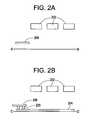
- FIG. 2A plan view of one embodiment of an inducting device 200 of the present invention is illustrated in FIG. 2 .
- the inducting device 200includes conductive turns 202 , patterned shield sections 204 , gaps 203 and shield tap 208 .
- Shield tap 208is coupled to shield tap terminal 210 .
- Shield tap terminal 210is typically coupled to AC ground but may be coupled to other locations depending on the requirements of a circuit the inducting device 200 is associated with.
- the present inventionincludes ribs 206 . Each rib 206 is coupled to an associated section of shield 204 and to shield tap 208 .
- the location of the various elements of the inducting device in vertical relation to each otheris illustrated in FIGS. 2A through 2C .
- FIG. 2Aa cross-sectional view along line AB of FIG. 2 is illustrated.
- the conductive turns 202 and shield tap 208are illustrated in FIG. 2 A. In between the conductive turns 202 and shield tap 208 is dielectric material.
- FIG. 2Ba cross-sectional view along line CD of FIG. 2 is illustrated. Besides the conductive turns 202 and the shield tap 208 , this view also illustrates a section of shield 204 and contacts 220 . Contacts 220 electrically couple the shield tap 208 to the section of shield 204 .
- FIG. 2Ca cross-sectional view along line EF of FIG. 2 is illustrated.
- FIG. 2Cillustrates the conductive turns 202 and a section of shield 204 .
- FIG. 2Cfurther illustrates rib 206 . Rib 206 is electrically coupled to shield section 204 via contacts 230 .
- the shield sections 204are conductive. In the embodiment of FIG. 2 , each shield section 204 conducts shield current primarily radially from below the conductive turns 202 to shield tap 208 . As illustrated, the shield tap 208 is an incomplete conductive ring. That is, a conductive ring that has at least one gap to prevent countercurrent. By providing an alternative low-resistance path to a shield terminal 210 and then typically to ground, the shield sections 240 and shield tap 208 significantly reduce losses caused by capacitively induced current through the semiconductor substrate.
- the plurality of conducting ribs 206 or (conducting strips 206 )are used to lower the parasitic resistance.
- the ribs 206are made from a material that is more conductive than the patterned shield sections 204 .
- Each rib 206is made from a layer of conductive material that is positioned between the conductive turns 202 and an associated section of shield 204 .
- each rib 206is electrically coupled to an associated section of shield 204 . That is, each rib 206 is only coupled to its associated shield section 204 .
- Each rib 206is further coupled to the shield tap 208 .
- the shield tap 208extends around and is coupled to an outer perimeter of the ribs 206 .
- the ribs 206greatly reduce the overall shield resistance by giving the shield current in each associated section of shield 204 a less resistive path to the shield tap 208 .
- the addition of the ribbing 206 closer to the conductive turns 208will introduce additional capacitance from the metal spiral layer to the shield structure (shield sections 204 , ribs 206 , and shield taps 208 ), this additional capacitance can be minimized by making each rib 206 relatively thin with respect to its associated shield section 204 . That is, each rib 206 is patterned or formed to have less of a lateral width than a lateral width of its associated shield section 204 . Further stated another way, the additional capacitance is reduced by forming each rib 206 to take up less lateral area than its associated shield section 204 .
- the shield layerhas many times the resistivity of metal. Shields of this resistivity have been very useful with overall shield resistances on the order of 1 ohm. Simulations varying the shield resistance show that Q can be improved by a further reduction in resistance. In fact, the shield resistance can be reduced by a factor of 3 or more with the addition of the ribs 206 of the present invention.
- the ribsare formed from a layer that is separated from the shield layer by a layer of dielectric.
- contactsare formed through the dielectric layer to provide electrical current paths between the ribs and the shield.
- FIGS. 3A through 3Fpartial cross-sectional views illustrating methods of forming ribs of the present invention of this embodiment is illustrated.
- a shield layer 304is formed over a lossy substrate 302 .
- the shield layer 304is formed by a silicide process.
- the shield layer 304is formed by implantation and yet in another embodiment the shield layer 304 is formed by diffusion.
- the shield layer 302is then patterned into sections of shield by gaps 306 or trenches 306 as illustrated in FIG. 3 B.
- shield sections 304 A and 304 Bare shown in FIG. 3 B.
- the trenches 306are formed by first removing material (portions of shield layer 304 and substrate 302 ) to form holes where the trenches 306 are to be positioned by some type of etch or similar technique. A thin coating film of oxide is then formed in the holes. The holes are then filled with silicon to form the trenches 306 .
- a dielectric layer 308is then formed overlaying the shield sections 304 A and 304 B as illustrated in FIG. 3 B.
- Contacts 310are formed though dielectric layer 308 .
- portions of dielectric layer 308are removed where the contacts 310 are to be positioned and then filled with a conductive material.
- the holes where the contacts 310 are to be formedare filled with conductive material when a subsequent conductive layer is formed overlaying the dielectric layer 308 .
- the ribsare then formed overlaying dielectric layer 308 .
- FIG. 3Cillustrates ribs 312 A and 312 B.
- ribs 312 A and 312 Bare formed by patterning one or more metal layers.
- ribs 312 A and 312 Bare formed in a conductive layer that is more conductive than the shield sections 304 A and 304 B.
- Contacts 310electrically couple each rib to an associated shield section 304 A or 304 B.
- rib 312 Ais electrically coupled to shield section 304 A and rib 312 B is electrically coupled to shield section 304 B.
- Dielectric layer 314is then formed over ribs 312 A and 312 B as illustrated in FIG. 3 E.
- the conductive turns 316are then formed.
- the turns 316are patterned from a main metal layer that is deposited over dielectric layer 314 .
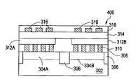
- FIG. 3Fa cross sectional view of one embodiment of a spiral inductor device 300 of the present invention is illustrated.
- a protective dielectric layer 318is formed overlaying the conductive turns 316 thereby forming one embodiment of an inducting device 400 of the present invention.
- the shield sections 304 A and 304 Bare vertically positioned between the conductive turns 316 and the lossy substrate 302 .
- the ribs 312 A and 312 Bare vertically positioned between the conductive turns 316 and the shield sections 304 A and 304 B.
- the ribs 206are formed from a layer directly overlaying a shield layer (not shown).
- the shieldis formed from a polysilicon layer that overlays a working surface of a substrate.
- the ribsare composed of a metal silicide (silicide) at the surface of the polysilicon shield layer.
- the shield layeris formed with a doped layer a semiconductor substrate and the ribs are formed from a silicide layer overlaying the working surface of the substrate.
- the shield sectionsare formed from a silicide layer over a doped polysilicon layer and the ribs are formed from a metal layer. In yet another embodiment, the shield sections are formed from a metal silicide layer overlaying a doped layer in a substrate and the ribs are formed from a metal layer. In another embodiment, the shield sections are formed from a doped layer in a substrate and the ribs are formed from a doped polysilicon and metal silicide layer. In addition, in further embodiments, shield taps and ribs are formed from the same metal layer. In further yet another embodiment, shield taps are formed in a different metal layer than the ribs.
- FIG. 4a plan view of one embodiment of a shielding region 700 having ribs 702 of the present invention is illustrated.
- FIG. 4does not illustrate conductive turns for clarity purposes. The conductive turns would extend over the shield sections 706 .
- two shield taps 704 A and 704 Bare used.
- the shield taps 704 A and 704 Aeach have a shield tap terminal 708 A and 708 B respectfully.
- Respective shield sections 706 and ribs 702are coupled to a respective shield tap 704 A or 704 B.
- FIG. 5Another example of a shielding region 800 having ribs 802 of one embodiment of the present invention is illustrated in the plan view of FIG. 5 .
- shield tap 806is coupled to shield sections 804 and 802 at an interior location.
- shield currentis directed radially inward to the shield tap 806 and then out through shield tap terminal 808 .
- the conductive turnsare not illustrated in FIG. 5 for clarifying purposes.
- the ribsextend inward beyond their associated shield sections in connecting to a shield tap.
- the ribsdo not extend across the entire length of their associated shield sections.
- each rib 902is coupled to an associated shield section 904 .
- the shield tap 906 of this embodimentforms an X shape and is coupled to each rib 902 and each section of shield.
- the conductive turns that form the inducting device 900are not shown for illustration purposes.
Landscapes
- Semiconductor Integrated Circuits (AREA)
- Internal Circuitry In Semiconductor Integrated Circuit Devices (AREA)
Abstract
Description
Claims (13)
Priority Applications (1)
| Application Number | Priority Date | Filing Date | Title |
|---|---|---|---|
| US10/740,548US6905889B2 (en) | 2002-07-11 | 2003-12-22 | Inductor device with patterned ground shield and ribbing |
Applications Claiming Priority (2)
| Application Number | Priority Date | Filing Date | Title |
|---|---|---|---|
| US10/194,496US6756656B2 (en) | 2002-07-11 | 2002-07-11 | Inductor device with patterned ground shield and ribbing |
| US10/740,548US6905889B2 (en) | 2002-07-11 | 2003-12-22 | Inductor device with patterned ground shield and ribbing |
Related Parent Applications (1)
| Application Number | Title | Priority Date | Filing Date |
|---|---|---|---|
| US10/194,496DivisionUS6756656B2 (en) | 2002-07-11 | 2002-07-11 | Inductor device with patterned ground shield and ribbing |
Publications (2)
| Publication Number | Publication Date |
|---|---|
| US20040183156A1 US20040183156A1 (en) | 2004-09-23 |
| US6905889B2true US6905889B2 (en) | 2005-06-14 |
Family
ID=30114758
Family Applications (2)
| Application Number | Title | Priority Date | Filing Date |
|---|---|---|---|
| US10/194,496Expired - LifetimeUS6756656B2 (en) | 2002-07-11 | 2002-07-11 | Inductor device with patterned ground shield and ribbing |
| US10/740,548Expired - LifetimeUS6905889B2 (en) | 2002-07-11 | 2003-12-22 | Inductor device with patterned ground shield and ribbing |
Family Applications Before (1)
| Application Number | Title | Priority Date | Filing Date |
|---|---|---|---|
| US10/194,496Expired - LifetimeUS6756656B2 (en) | 2002-07-11 | 2002-07-11 | Inductor device with patterned ground shield and ribbing |
Country Status (1)
| Country | Link |
|---|---|
| US (2) | US6756656B2 (en) |
Cited By (32)
| Publication number | Priority date | Publication date | Assignee | Title |
|---|---|---|---|---|
| US20050021972A1 (en)* | 1999-04-15 | 2005-01-27 | Gilian Technologies Ltd. | Data quality assurance |
| US20070268093A1 (en)* | 2007-08-01 | 2007-11-22 | Chartered Semiconductor Manufacturing, Ltd. | Integrated circuit shield structure and method of fabrication thereof |
| US20080029854A1 (en)* | 2006-08-03 | 2008-02-07 | United Microelectronics Corp. | Conductive shielding pattern and semiconductor structure with inductor device |
| US20090020877A1 (en)* | 2007-07-16 | 2009-01-22 | Via Technologies, Inc. | Transmission line structure and signal transmission structure |
| US20090090995A1 (en)* | 2007-10-05 | 2009-04-09 | Taiwan Semiconductor Manufacturing Co., Ltd. | On-chip inductors with through-silicon-via fence for Q improvement |
| US20090250262A1 (en)* | 2008-04-03 | 2009-10-08 | Qualcomm Incorporated | Inductor with patterned ground plane |
| US20100019300A1 (en)* | 2008-06-25 | 2010-01-28 | The Trustees Of Columbia University In The City Of New York | Multilayer integrated circuit having an inductor in stacked arrangement with a distributed capacitor |
| US20110116208A1 (en)* | 2009-11-17 | 2011-05-19 | Signoff David M | Ground Shield Capacitor |
| US8395455B1 (en) | 2011-10-14 | 2013-03-12 | United Microelectronics Corp. | Ring oscillator |
| US8421509B1 (en) | 2011-10-25 | 2013-04-16 | United Microelectronics Corp. | Charge pump circuit with low clock feed-through |
| US8493806B1 (en) | 2012-01-03 | 2013-07-23 | United Microelectronics Corporation | Sense-amplifier circuit of memory and calibrating method thereof |
| US8588020B2 (en) | 2011-11-16 | 2013-11-19 | United Microelectronics Corporation | Sense amplifier and method for determining values of voltages on bit-line pair |
| US8643521B1 (en) | 2012-11-28 | 2014-02-04 | United Microelectronics Corp. | Digital-to-analog converter with greater output resistance |
| US8669897B1 (en) | 2012-11-05 | 2014-03-11 | United Microelectronics Corp. | Asynchronous successive approximation register analog-to-digital converter and operating method thereof |
| US8692608B2 (en) | 2011-09-19 | 2014-04-08 | United Microelectronics Corp. | Charge pump system capable of stabilizing an output voltage |
| US8711598B1 (en) | 2012-11-21 | 2014-04-29 | United Microelectronics Corp. | Memory cell and memory cell array using the same |
| US8724404B2 (en) | 2012-10-15 | 2014-05-13 | United Microelectronics Corp. | Memory, supply voltage generation circuit, and operation method of a supply voltage generation circuit used for a memory array |
| US8866536B1 (en) | 2013-11-14 | 2014-10-21 | United Microelectronics Corp. | Process monitoring circuit and method |
| US8873295B2 (en) | 2012-11-27 | 2014-10-28 | United Microelectronics Corporation | Memory and operation method thereof |
| US8917109B2 (en) | 2013-04-03 | 2014-12-23 | United Microelectronics Corporation | Method and device for pulse width estimation |
| US8947911B1 (en) | 2013-11-07 | 2015-02-03 | United Microelectronics Corp. | Method and circuit for optimizing bit line power consumption |
| US8953401B2 (en) | 2012-12-07 | 2015-02-10 | United Microelectronics Corp. | Memory device and method for driving memory array thereof |
| US8970197B2 (en) | 2012-08-03 | 2015-03-03 | United Microelectronics Corporation | Voltage regulating circuit configured to have output voltage thereof modulated digitally |
| US9030221B2 (en) | 2011-09-20 | 2015-05-12 | United Microelectronics Corporation | Circuit structure of test-key and test method thereof |
| US9030886B2 (en) | 2012-12-07 | 2015-05-12 | United Microelectronics Corp. | Memory device and driving method thereof |
| US9105355B2 (en) | 2013-07-04 | 2015-08-11 | United Microelectronics Corporation | Memory cell array operated with multiple operation voltage |
| US9143143B2 (en) | 2014-01-13 | 2015-09-22 | United Microelectronics Corp. | VCO restart up circuit and method thereof |
| US9583554B1 (en) | 2014-12-23 | 2017-02-28 | Altera Corporation | Adjustable ground shielding circuitry |
| US9691720B2 (en) | 2015-07-27 | 2017-06-27 | Qualcomm Incorporated | Multi-layer ground shield structure of interconnected elements |
| US10672704B2 (en)* | 2017-11-30 | 2020-06-02 | Taiwan Semiconductor Manufacturing Company Ltd. | Semiconductor device with polygonal inductive device |
| US11004589B2 (en) | 2018-04-27 | 2021-05-11 | Realtek Semiconductor Corp. | High-Q integrated inductor and method thereof |
| US11152150B2 (en) | 2018-05-09 | 2021-10-19 | Realtek Semiconductor Corp. | LC tank circuit having improved resonant frequency stability and fabrication method thereof |
Families Citing this family (20)
| Publication number | Priority date | Publication date | Assignee | Title |
|---|---|---|---|---|
| US20050104158A1 (en)* | 2003-11-19 | 2005-05-19 | Scintera Networks, Inc. | Compact, high q inductor for integrated circuit |
| US7084728B2 (en)* | 2003-12-15 | 2006-08-01 | Nokia Corporation | Electrically decoupled integrated transformer having at least one grounded electric shield |
| US7243321B2 (en)* | 2004-04-07 | 2007-07-10 | Cadence Design Systems, Inc. | IC layout physical verification method |
| US7663205B2 (en)* | 2004-08-03 | 2010-02-16 | Samsung Electronics Co., Ltd. | Integrated circuit devices including a dummy gate structure below a passive electronic element |
| US11201500B2 (en) | 2006-01-31 | 2021-12-14 | Mojo Mobility, Inc. | Efficiencies and flexibilities in inductive (wireless) charging |
| TWI349362B (en)* | 2007-12-07 | 2011-09-21 | Realtek Semiconductor Corp | Integrated inductor |
| US20110050164A1 (en) | 2008-05-07 | 2011-03-03 | Afshin Partovi | System and methods for inductive charging, and improvements and uses thereof |
| US9142342B2 (en)* | 2010-05-17 | 2015-09-22 | Ronald Lambert Haner | Compact-area capacitive plates for use with spiral inductors having more than one turn |
| WO2011156768A2 (en) | 2010-06-11 | 2011-12-15 | Mojo Mobility, Inc. | System for wireless power transfer that supports interoperability, and multi-pole magnets for use therewith |
| US11342777B2 (en) | 2011-01-18 | 2022-05-24 | Mojo Mobility, Inc. | Powering and/or charging with more than one protocol |
| US8791732B2 (en) | 2011-05-09 | 2014-07-29 | Mediatek Inc. | Phase locked loop |
| US20120286391A1 (en)* | 2011-05-09 | 2012-11-15 | Mediatek Inc. | Semiconductor circuit |
| US9318432B2 (en)* | 2012-10-31 | 2016-04-19 | Qualcomm Technologies International, Ltd. | Shielded system |
| CN104241242B (en)* | 2013-06-09 | 2017-12-29 | 中芯国际集成电路制造(上海)有限公司 | Earth shield structure and semiconductor devices |
| US9646759B1 (en) | 2014-04-11 | 2017-05-09 | Altera Corporation | LC tank circuitry with shielding structures |
| US10109584B2 (en)* | 2014-09-02 | 2018-10-23 | Qualcomm Incorporated | Patterned grounds and methods of forming the same |
| US11444485B2 (en) | 2019-02-05 | 2022-09-13 | Mojo Mobility, Inc. | Inductive charging system with charging electronics physically separated from charging coil |
| TWI713188B (en)* | 2019-09-24 | 2020-12-11 | 瑞昱半導體股份有限公司 | Patterned shielding structure |
| CN112582379B (en)* | 2019-09-30 | 2024-12-24 | 瑞昱半导体股份有限公司 | Patterned shielding structure |
| CN114974845A (en)* | 2021-02-26 | 2022-08-30 | 瑞昱半导体股份有限公司 | Shielding structure and inductor device |
Citations (7)
| Publication number | Priority date | Publication date | Assignee | Title |
|---|---|---|---|---|
| US5717243A (en)* | 1996-04-24 | 1998-02-10 | Harris Corporation | Integrated circuit with an improved inductor structure and method of fabrication |
| US20020093414A1 (en)* | 2001-01-17 | 2002-07-18 | Winbond Electronics Corporation | Patterned ground shield for mirror current elimination |
| US6437409B2 (en) | 2000-02-14 | 2002-08-20 | Nec Corporation | Semiconductor device |
| US6486529B2 (en)* | 2001-03-05 | 2002-11-26 | Taiwan Semiconductor Manufacturing Company | Structure of merged vertical capacitor inside spiral conductor for RF and mixed-signal applications |
| US6593838B2 (en) | 2000-12-19 | 2003-07-15 | Atheros Communications Inc. | Planar inductor with segmented conductive plane |
| US6635949B2 (en)* | 2002-01-04 | 2003-10-21 | Intersil Americas Inc. | Symmetric inducting device for an integrated circuit having a ground shield |
| US6815220B2 (en)* | 1999-11-23 | 2004-11-09 | Intel Corporation | Magnetic layer processing |
- 2002
- 2002-07-11USUS10/194,496patent/US6756656B2/ennot_activeExpired - Lifetime
- 2003
- 2003-12-22USUS10/740,548patent/US6905889B2/ennot_activeExpired - Lifetime
Patent Citations (7)
| Publication number | Priority date | Publication date | Assignee | Title |
|---|---|---|---|---|
| US5717243A (en)* | 1996-04-24 | 1998-02-10 | Harris Corporation | Integrated circuit with an improved inductor structure and method of fabrication |
| US6815220B2 (en)* | 1999-11-23 | 2004-11-09 | Intel Corporation | Magnetic layer processing |
| US6437409B2 (en) | 2000-02-14 | 2002-08-20 | Nec Corporation | Semiconductor device |
| US6593838B2 (en) | 2000-12-19 | 2003-07-15 | Atheros Communications Inc. | Planar inductor with segmented conductive plane |
| US20020093414A1 (en)* | 2001-01-17 | 2002-07-18 | Winbond Electronics Corporation | Patterned ground shield for mirror current elimination |
| US6486529B2 (en)* | 2001-03-05 | 2002-11-26 | Taiwan Semiconductor Manufacturing Company | Structure of merged vertical capacitor inside spiral conductor for RF and mixed-signal applications |
| US6635949B2 (en)* | 2002-01-04 | 2003-10-21 | Intersil Americas Inc. | Symmetric inducting device for an integrated circuit having a ground shield |
Non-Patent Citations (2)
| Title |
|---|
| "Handbook of Semiconductor Silicon Technology," eds. William C. O'Mara, Robert B. Herring, and Lee P. Hunt, Noyes Publications., Norwich, New York, (reprint edition 1990), pp. 700-702. |
| "Semiconductor Materials and Process Technology Handbook for Very Large Scale Integration (VLSI) and Ultra Large Scale Integration (ULSI)," ed. Gary E. McGuire, Noyes Publications, Norwich, New York, (1988) p. 439. |
Cited By (41)
| Publication number | Priority date | Publication date | Assignee | Title |
|---|---|---|---|---|
| US7552196B2 (en)* | 1999-04-15 | 2009-06-23 | Breach Security, Inc. | Detecting corrupted data before transmission to a client |
| US20050021972A1 (en)* | 1999-04-15 | 2005-01-27 | Gilian Technologies Ltd. | Data quality assurance |
| US20080029854A1 (en)* | 2006-08-03 | 2008-02-07 | United Microelectronics Corp. | Conductive shielding pattern and semiconductor structure with inductor device |
| US20090020877A1 (en)* | 2007-07-16 | 2009-01-22 | Via Technologies, Inc. | Transmission line structure and signal transmission structure |
| US20100120244A1 (en)* | 2007-08-01 | 2010-05-13 | Chartered Semiconductor Manufacturing, Ltd. | Integrated circuit shield structure and method of fabrication thereof |
| US7652355B2 (en)* | 2007-08-01 | 2010-01-26 | Chartered Semiconductor Manufacturing, Ltd. | Integrated circuit shield structure |
| US8003529B2 (en) | 2007-08-01 | 2011-08-23 | Globalfoundries Singapore Pte. Ltd. | Method of fabrication an integrated circuit |
| US20070268093A1 (en)* | 2007-08-01 | 2007-11-22 | Chartered Semiconductor Manufacturing, Ltd. | Integrated circuit shield structure and method of fabrication thereof |
| US20090090995A1 (en)* | 2007-10-05 | 2009-04-09 | Taiwan Semiconductor Manufacturing Co., Ltd. | On-chip inductors with through-silicon-via fence for Q improvement |
| US8492872B2 (en)* | 2007-10-05 | 2013-07-23 | Taiwan Semiconductor Manufacturing Co., Ltd. | On-chip inductors with through-silicon-via fence for Q improvement |
| US20090250262A1 (en)* | 2008-04-03 | 2009-10-08 | Qualcomm Incorporated | Inductor with patterned ground plane |
| US8559186B2 (en) | 2008-04-03 | 2013-10-15 | Qualcomm, Incorporated | Inductor with patterned ground plane |
| US20100019300A1 (en)* | 2008-06-25 | 2010-01-28 | The Trustees Of Columbia University In The City Of New York | Multilayer integrated circuit having an inductor in stacked arrangement with a distributed capacitor |
| US20110116208A1 (en)* | 2009-11-17 | 2011-05-19 | Signoff David M | Ground Shield Capacitor |
| US8988852B2 (en)* | 2009-11-17 | 2015-03-24 | Marvell World Trade Ltd. | Ground shield capacitor |
| US8692608B2 (en) | 2011-09-19 | 2014-04-08 | United Microelectronics Corp. | Charge pump system capable of stabilizing an output voltage |
| US9030221B2 (en) | 2011-09-20 | 2015-05-12 | United Microelectronics Corporation | Circuit structure of test-key and test method thereof |
| US8395455B1 (en) | 2011-10-14 | 2013-03-12 | United Microelectronics Corp. | Ring oscillator |
| US8421509B1 (en) | 2011-10-25 | 2013-04-16 | United Microelectronics Corp. | Charge pump circuit with low clock feed-through |
| US8588020B2 (en) | 2011-11-16 | 2013-11-19 | United Microelectronics Corporation | Sense amplifier and method for determining values of voltages on bit-line pair |
| US8493806B1 (en) | 2012-01-03 | 2013-07-23 | United Microelectronics Corporation | Sense-amplifier circuit of memory and calibrating method thereof |
| US8970197B2 (en) | 2012-08-03 | 2015-03-03 | United Microelectronics Corporation | Voltage regulating circuit configured to have output voltage thereof modulated digitally |
| US8804440B1 (en) | 2012-10-15 | 2014-08-12 | United Microelectronics Corporation | Memory for a voltage regulator circuit |
| US8767485B1 (en) | 2012-10-15 | 2014-07-01 | United Microelectronics Corp. | Operation method of a supply voltage generation circuit used for a memory array |
| US8724404B2 (en) | 2012-10-15 | 2014-05-13 | United Microelectronics Corp. | Memory, supply voltage generation circuit, and operation method of a supply voltage generation circuit used for a memory array |
| US8669897B1 (en) | 2012-11-05 | 2014-03-11 | United Microelectronics Corp. | Asynchronous successive approximation register analog-to-digital converter and operating method thereof |
| US8711598B1 (en) | 2012-11-21 | 2014-04-29 | United Microelectronics Corp. | Memory cell and memory cell array using the same |
| US8873295B2 (en) | 2012-11-27 | 2014-10-28 | United Microelectronics Corporation | Memory and operation method thereof |
| US8643521B1 (en) | 2012-11-28 | 2014-02-04 | United Microelectronics Corp. | Digital-to-analog converter with greater output resistance |
| US9030886B2 (en) | 2012-12-07 | 2015-05-12 | United Microelectronics Corp. | Memory device and driving method thereof |
| US8953401B2 (en) | 2012-12-07 | 2015-02-10 | United Microelectronics Corp. | Memory device and method for driving memory array thereof |
| US8917109B2 (en) | 2013-04-03 | 2014-12-23 | United Microelectronics Corporation | Method and device for pulse width estimation |
| US9105355B2 (en) | 2013-07-04 | 2015-08-11 | United Microelectronics Corporation | Memory cell array operated with multiple operation voltage |
| US8947911B1 (en) | 2013-11-07 | 2015-02-03 | United Microelectronics Corp. | Method and circuit for optimizing bit line power consumption |
| US8866536B1 (en) | 2013-11-14 | 2014-10-21 | United Microelectronics Corp. | Process monitoring circuit and method |
| US9143143B2 (en) | 2014-01-13 | 2015-09-22 | United Microelectronics Corp. | VCO restart up circuit and method thereof |
| US9583554B1 (en) | 2014-12-23 | 2017-02-28 | Altera Corporation | Adjustable ground shielding circuitry |
| US9691720B2 (en) | 2015-07-27 | 2017-06-27 | Qualcomm Incorporated | Multi-layer ground shield structure of interconnected elements |
| US10672704B2 (en)* | 2017-11-30 | 2020-06-02 | Taiwan Semiconductor Manufacturing Company Ltd. | Semiconductor device with polygonal inductive device |
| US11004589B2 (en) | 2018-04-27 | 2021-05-11 | Realtek Semiconductor Corp. | High-Q integrated inductor and method thereof |
| US11152150B2 (en) | 2018-05-09 | 2021-10-19 | Realtek Semiconductor Corp. | LC tank circuit having improved resonant frequency stability and fabrication method thereof |
Also Published As
| Publication number | Publication date |
|---|---|
| US20040007760A1 (en) | 2004-01-15 |
| US20040183156A1 (en) | 2004-09-23 |
| US6756656B2 (en) | 2004-06-29 |
Similar Documents
| Publication | Publication Date | Title |
|---|---|---|
| US6905889B2 (en) | Inductor device with patterned ground shield and ribbing | |
| US6900087B2 (en) | Symmetric inducting device for an integrated circuit having a ground shield | |
| US7332793B2 (en) | Semiconductor device | |
| US8653926B2 (en) | Inductive and capacitive elements for semiconductor technologies with minimum pattern density requirements | |
| US6879022B2 (en) | Inductance device formed on semiconductor substrate | |
| US9224827B2 (en) | High voltage resistor | |
| US7834403B2 (en) | Bipolar transistor FINFET technology | |
| EP1267391B1 (en) | A method to fabricate RF inductors with minimum area | |
| US8785987B2 (en) | IGFET device having an RF capability | |
| US20020050626A1 (en) | Semiconductor device and manufacturing method therefor | |
| US20060273372A1 (en) | Lateral lubistor structure and method | |
| US6803849B2 (en) | Solid state inducting device | |
| US12183804B2 (en) | RF switch device with a sidewall spacer having a low dielectric constant | |
| US5918121A (en) | Method of reducing substrate losses in inductor | |
| JP2002305110A (en) | Integrated circuit inductance structure | |
| US7154161B1 (en) | Composite ground shield for passive components in a semiconductor die | |
| US20020142526A1 (en) | Structures and methods to minimize plasma charging damage in silicon on insulator devices | |
| US6538281B2 (en) | Low on-resistance LDMOS | |
| US20100164672A1 (en) | Semiconductor device and method for manufacturing the same | |
| US20240355731A1 (en) | Active region electrically programmable fuse with gate structure as silicide block | |
| JP7545503B2 (en) | Semiconductor Devices | |
| US7053454B1 (en) | Semiconductor component, method for producing the semiconductor component, and method for producing electrical connections between individual circuit elements | |
| CN115881689A (en) | Semiconductor device with a plurality of transistors |
Legal Events
| Date | Code | Title | Description |
|---|---|---|---|
| STCF | Information on status: patent grant | Free format text:PATENTED CASE | |
| AS | Assignment | Owner name:BANK OF NEW YORK TRUST COMPANY, N.A.,ILLINOIS Free format text:SECURITY INTEREST;ASSIGNOR:CONEXANT, INC.;REEL/FRAME:018545/0298 Effective date:20061113 Owner name:BANK OF NEW YORK TRUST COMPANY, N.A., ILLINOIS Free format text:SECURITY INTEREST;ASSIGNOR:CONEXANT, INC.;REEL/FRAME:018545/0298 Effective date:20061113 | |
| AS | Assignment | Owner name:INTERSIL AMERICAS, INC., CALIFORNIA Free format text:ASSIGNMENT OF ASSIGNORS INTEREST;ASSIGNOR:LOWTHER, REX EVERETT;REEL/FRAME:021006/0923 Effective date:20020711 Owner name:GLOBESPANVIRATA, INC., NEW JERSEY Free format text:ASSIGNMENT OF ASSIGNORS INTEREST;ASSIGNORS:INTERSIL CORPORATION;INTERSIL AMERICAS, INC.;REEL/FRAME:021006/0931 Effective date:20030715 Owner name:CONEXANT, INC., NEW JERSEY Free format text:CHANGE OF NAME;ASSIGNOR:GLOBESPANVIRATA, INC.;REEL/FRAME:021006/0744 Effective date:20040528 | |
| FPAY | Fee payment | Year of fee payment:4 | |
| AS | Assignment | Owner name:CONEXANT, INC., CALIFORNIA Free format text:RELEASE BY SECURED PARTY;ASSIGNOR:BANK OF NEW YORK MELLON TRUST COMPANY, N.A. (FORMERLY, BANK OF NEW YORK TRUST COMPANY, N.A.);REEL/FRAME:021731/0845 Effective date:20081017 Owner name:CONEXANT, INC.,CALIFORNIA Free format text:RELEASE BY SECURED PARTY;ASSIGNOR:BANK OF NEW YORK MELLON TRUST COMPANY, N.A. (FORMERLY, BANK OF NEW YORK TRUST COMPANY, N.A.);REEL/FRAME:021731/0845 Effective date:20081017 | |
| AS | Assignment | Owner name:XOCYST TRANSFER AG L.L.C., DELAWARE Free format text:ASSIGNMENT OF ASSIGNORS INTEREST;ASSIGNOR:CONEXANT, INC.;REEL/FRAME:022043/0591 Effective date:20081016 Owner name:XOCYST TRANSFER AG L.L.C.,DELAWARE Free format text:ASSIGNMENT OF ASSIGNORS INTEREST;ASSIGNOR:CONEXANT, INC.;REEL/FRAME:022043/0591 Effective date:20081016 | |
| FEPP | Fee payment procedure | Free format text:PAYOR NUMBER ASSIGNED (ORIGINAL EVENT CODE: ASPN); ENTITY STATUS OF PATENT OWNER: LARGE ENTITY | |
| AS | Assignment | Owner name:INTELLECTUAL VENTURES I LLC, DELAWARE Free format text:MERGER;ASSIGNOR:XOCYST TRANSFER AG L.L.C.;REEL/FRAME:026637/0603 Effective date:20110718 | |
| FPAY | Fee payment | Year of fee payment:8 | |
| FPAY | Fee payment | Year of fee payment:12 |