US6905392B2 - Polishing system having a carrier head with substrate presence sensing - Google Patents
Polishing system having a carrier head with substrate presence sensingDownload PDFInfo
- Publication number
- US6905392B2 US6905392B2US10/609,996US60999603AUS6905392B2US 6905392 B2US6905392 B2US 6905392B2US 60999603 AUS60999603 AUS 60999603AUS 6905392 B2US6905392 B2US 6905392B2
- Authority
- US
- United States
- Prior art keywords
- substrate
- plunger
- plate
- holding mechanism
- carrier head
- Prior art date
- Legal status (The legal status is an assumption and is not a legal conclusion. Google has not performed a legal analysis and makes no representation as to the accuracy of the status listed.)
- Expired - Lifetime
Links
Images


Classifications
- B—PERFORMING OPERATIONS; TRANSPORTING
- B24—GRINDING; POLISHING
- B24B—MACHINES, DEVICES, OR PROCESSES FOR GRINDING OR POLISHING; DRESSING OR CONDITIONING OF ABRADING SURFACES; FEEDING OF GRINDING, POLISHING, OR LAPPING AGENTS
- B24B37/00—Lapping machines or devices; Accessories
- B24B37/27—Work carriers
- B24B37/30—Work carriers for single side lapping of plane surfaces
- B—PERFORMING OPERATIONS; TRANSPORTING
- B24—GRINDING; POLISHING
- B24B—MACHINES, DEVICES, OR PROCESSES FOR GRINDING OR POLISHING; DRESSING OR CONDITIONING OF ABRADING SURFACES; FEEDING OF GRINDING, POLISHING, OR LAPPING AGENTS
- B24B37/00—Lapping machines or devices; Accessories
- B24B37/005—Control means for lapping machines or devices
- B24B37/0053—Control means for lapping machines or devices detecting loss or breakage of a workpiece during lapping
Definitions
- the inventionrelates generally to the field of semiconductor manufacturing, and more specifically to a polishing system having a carrier head with substrate presence sensing.
- a wafer carrieris a critical component of a polisher.
- the wafer carrierserves two main purposes.
- a first purposeis to transport a wafer to/from a load station and between each polishing process area.
- a second purposeis to press the wafer downward against a polishing pad using a backside pressure while the polish pad and the wafer carrier rotate at high speeds.
- the type of carrierdetermines how pressure is applied to the backside of the wafer.
- One type of carrierincludes an internal wafer presence sensor to verify that a wafer is loaded onto the carrier.
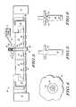
- FIG. 1is a cross sectional view of a carrier head having a substrate sensing mechanism according to the prior art.
- Carrier head 10includes a perforated plate 12 , and a gimbal plate 14 disposed within retaining ring 16 .
- An edge control ring 20holds a membrane 22 across a bottom surface of perforated plate 12 .
- the substrate sensing mechanism of carrier head 10includes a plunger 24 disposed within a sensor venting port 50 of gimbal plate 14 .
- Plunger 24is resiliently held within the venting port by a weak spring 26 disposed between a top portion of plunger 24 and an encapsulated region defined by reference numeral 28 .
- An oversized non-captured O-ring 30is disposed between a flange portion of the plunger 24 and a top surface of gimbal plate 14 , around the venting port 50 .
- Pressure sensor 32monitors a pressure within encapsulated region 28 . Under normal operating conditions, encapsulated region 28 is either pressurized or vented.
- Plunger 24can move vertically within sensor venting port 50 between a lower most travel position and an upper most travel position.
- the lower most travel positionis defined by a combination of the plunger flange, the oversized non-captured O-ring 30 , and the top surface of the gimbal plate 14 .
- a bottom portion of plunger 24extends below a lower most surface of perforated plate 12 by a distance indicated by reference numeral 36 .
- the upper most travel positionis defined by a top surface of the plunger flange and a surface above the flange within encapsulated region 28 .
- a top portion of the plunger 24is moved a distance as indicated by reference numeral 34 .
- FIG. 2is a top view of a substrate sensor venting port and an oversized non-captured O-ring according to the prior art.
- a portion of gimbal plate 14 containing the substrate sensor venting port 50is shown.
- the diameter of venting port 50is slightly larger than a diameter of the plunger 24 to allow the plunger 24 to move within port 50 .
- venting arteries or channels 52are disposed along an inner sidewall of port 50 , extending from a top surface of gimbal plate 14 to a bottom surface of gimbal plate 14 .
- the use of the oversized non-captured O-ring 30increases a possibility for impeding the venting of the encapsulated region, resulting in an erroneous sensing performance.
- O-ring 30is subject to various placements about the venting port 50 , for example, off-center from the venting port 50 . It is also possible for the placement of O-ring 30 to preclude passage of vacuum or pressure through one or more arteries 52 .
- Carrier head 10suffers from reliability issues of the wafer sensing mechanism. Such reliability issues lead to various handling problems that include one or more of dechuck errors, false wafer loss alarms, and failure to detect wafer loss.
- a dechuck errorgenerally refers to a situation wherein a wafer slips off the carrier onto the underlying polishing pad as the carrier attempts to lift off the polishing pad after processing, typically resulting in breakage of the wafer.
- a false wafer loss alarmgenerally refers to a situation wherein the carrier incorrectly senses no wafer presence although a wafer is physically loaded, typically resulting in various handling errors.
- a failure to detect wafer lossgenerally refers to a situation wherein the carrier incorrectly senses a wafer when a wafer is not physically present, typically resulting in wafer breakage of a wafer that gets left behind.
- Such problemscause product scrap, tool downtime/reduced availability, and increased wafer polishing and carrier consumable cost.
- a system for polishing a substrateincludes a controller, a platen, and a carrier head.
- the carrier headis coupled to the controller.
- the carrier headis for carrying the substrate and holding the substrate against the platen during polishing.
- the carrier headincludes a retaining ring for laterally supporting the substrate, a holding mechanism for applying positive pressure to the substrate during polishing and negative pressure when carrying the substrate, a gimbal plate coupled to the holding mechanism, and substrate detection means, coupled to the gimbal plate for detecting if the substrate is secured by the holding mechanism when the holding mechanism is applying negative pressure.
- the substrate detection meansincludes a plunger passing through a hole in the gimbal plate.
- the plungerhas a maximum travel distance in the hole, has a bottom surface that extends below the gimbal plate and is coupled to the substrate during detecting.
- the plungerextends past the holding mechanism by an amount substantially equal to the maximum travel distance of the plunger.
- FIG. 1is a cross sectional view of a carrier head having a substrate sensing mechanism according to the prior art
- FIG. 2is a top view of a substrate sensor venting port and an oversized non-captured O-ring according to the prior art
- FIG. 3is a cross sectional view of a carrier head with a substrate presence sensing mechanism according to an embodiment of the present disclosure
- FIG. 4is a top view of a substrate sensor venting port and a captured compliant sealing ring according to an embodiment of the present disclosure
- FIG. 5is a section view of a substrate sensing plunger according to an embodiment of the present disclosure.
- FIG. 6is a section view of a substrate sensing plunger with a captured sealing ring according to an embodiment of the present disclosure.
- FIG. 7is a block diagram view of a polishing system having a carrier head with substrate presence sensing according to an embodiment of the present disclosure.
- FIG. 3is a cross sectional view of a carrier head with a substrate presence sensing mechanism according to an embodiment of the present disclosure.
- Carrier head 38includes a perforated plate 40 , and a gimbal plate 14 disposed within retaining ring 16 .
- An edge control ring 20holds a membrane 22 across a bottom surface of perforated plate 40 .
- the perforated plate 40has a thickness on the order of 0.100+/ ⁇ 0.005 in. Such a thickness enables an optimal wafer sense plunger extension, allowing the wafer sensor to vent the membrane 22 when a wafer is physically present.
- the substrate sensing mechanism of carrier head 38includes a plunger 46 disposed within a sensor venting port 50 of gimbal plate 14 .
- Plunger 46is resiliently held within the venting port by spring 42 disposed between a top portion of plunger 46 and an encapsulated region defined by reference numeral 28 .
- a captured resilient sealing ring 44is disposed between a flange portion of the plunger 46 and a top surface of gimbal plate 14 , around the venting port 50 .
- Sealing ring 44includes any suitable resilient material capable of withstanding polishing process conditions, as appropriate.
- Pressure sensor 32monitors a pressure within encapsulated region 28 . Under normal operating conditions, encapsulated region 28 is either pressurized or vented.
- Spring 42is a spring of sufficient strength for sealing with the captured resilient sealing ring 44 , the chamber defined by the encapsulated region 28 , and the region between the bottom portion of the gimbal plate 14 and the membrane 22 .
- Spring 42is selected to also provide a sufficient force such that in response to pulling a vacuum on the membrane 22 , in the absence of a substrate, the membrane 22 does not overcome the force provided by spring 42 , and accordingly, does not breach the seal provided by the sealing ring 44 and the top of plate 14 . Still further, spring 42 must allow the sensor to be depressed in the event of pulling vacuum on a substrate, wherein the substrate acts upon the plunger 46 , breaking the seal otherwise provided by the sealing ring 44 and the top of plate 14 .
- Spring 42must also not prevent a bottom portion of plunger 46 from aligning flush with a bottom side of perforated plate 40 .
- spring 42has a stiffness rating on the order of 19+/ ⁇ 5 lb/in, which allows wafer sensor actuation even under the highest possible membrane vacuum setting, while reliably actuating during physical wafer presence.
- Plunger 46can move vertically within sensor venting port 50 between a lower most travel position and an upper most travel position.
- the lower most travel positionis defined by a combination of the plunger flange, the captured resilient sealing ring 44 , and the top surface of the gimbal plate 14 .
- a bottom portion of plunger 46extends below a lower most surface of perforated plate 40 by a distance indicated by reference numeral 48 . Note that the distance 48 is greater than the distance 36 , shown in FIG. 1 .
- the upper most travel positionis defined by a top surface of the plunger flange and a surface above the flange within encapsulated region 28 .
- a top portion of the plunger 46is moved a distance as indicated by reference numeral 34 .
- distance 48must be less than or equal to distance 34 .
- FIG. 4is a top view of a substrate sensor venting port and a captured compliant sealing ring according to an embodiment of the present disclosure.
- a portion of gimbal plate 14 containing the substrate sensor venting port 50is shown.
- the diameter of venting port 50is slightly larger than a diameter of the plunger 46 to allow the plunger 46 to move within port 50 .
- venting arteries or channels 53are disposed along an inner sidewall of port 50 , extending from a top surface of gimbal plate 14 to a bottom surface of gimbal plate 14 .
- plunger 46captures resilient sealing ring 44 in a manner which makes the captured resilient sealing ring 44 subject to repeatable placement about and on-center with the venting port 50 . Accordingly, the placement of captured resilient sealing ring 44 assures both the passing and the blocking of vacuum or pressure, as needed, through arteries 53 .
- arteries 53are constructed to have equal or greater area than the orifice 55 between encapsulated region 28 and pressure sensor 32 .
- orifice 55may have an orifice size within encapsulated region 28 on the order of approximately 0.050′′ in diameter.
- the size of the three arteries 53can each be on the order of an approximately 0.025′′ radius half circle.
- a benefit of the increased volume provided by arteries 53can be understood from the following illustration.
- the encapsulated region 28is under positive pressure.
- the waferpresses against the wafer sensor.
- the vacuum within the membrane areamust overcome the positive pressure and cause a delta-pressure on sensor 32 .
- a threshold on the order of approximately 0.8 to 1.0 Vdc on sensor 32can be obtained, in contrast to a threshold on the order of approximately 0.3 to 0.5 Vdc with known wafer sensor embodiments.
- a tool constant value on the order of approximately 0.5 Vdccan be used, in comparison to a tool constant value on the order of 0.2 Vdc of a known wafer sensor embodiments. Accordingly, the embodiments of the present disclosure provide more reliable sensing and greater confidence that a wafer is actually pressed against the sensor and removed from the pad, rather than in a transition of moving from the pad and against the sensor.
- FIG. 5is a section view of a substrate sensing plunger according to an embodiment of the present disclosure. More particularly, plunger 46 includes a top portion and a bottom portion, separated by a flange portion. Between the flange portion and the bottom portion, plunger 46 includes a recessed region 54 . The recessed region is adapted for receiving and capturing the resilient sealing ring 44 therein. Once captured, movement of the resilient sealing ring with respect to the venting port 50 is more precisely controlled by plunger 46 . Accordingly, a reliability of sensing the presence or absence of a semiconductor substrate is greatly enhanced.
- FIG. 6is a section view of a substrate sensing plunger with a captured sealing ring according to an embodiment of the present disclosure.
- resilient sealing ring 44is captured within recess 54 .
- a bottom portion of plunger 46has a first diameter, as indicated by reference numeral 56 .
- Recess 54has a second diameter, as indicated by reference numeral 58 .
- the second diameter 58is on the order of less than the first diameter 56 .
- diameter 58is on the order of slightly larger than an inner diameter of resilient sealing ring 44 .
- the inner diameter of resilient sealing ring 44is less than the diameter 56 of the bottom portion of plunger 46 .
- FIG. 7is a block diagram view of a polishing system having a carrier head with substrate presence sensing according to an embodiment of the present disclosure.
- Polishing system 60includes a carrier head 38 , a platen 62 , polishing pad 64 , motor 66 , one or more pressure sources ( 68 , 70 , 72 ), and controller 74 .
- Carrier head 38includes the substrate carrier head discussed herein above with respect to FIGS. 3 , 4 , 5 and 6 .
- Carrier head 38retains a substrate 76 within the retaining ring 16 during a polishing operation.
- a polishing operationgenerally includes a substrate attach/detach step and a substrate transport step, in addition to the substrate polishing.
- the carrier headtransports the substrate between a substrate loading and unloading position, as well as, transports the substrate from a non-contact polishing position (i.e., substrate not in contact with the polishing pad) to a contact polishing position (i.e., substrate in contact with the polishing pad), or vice versa.
- Substrate attachment and/or detachment prior to transportis accomplished with the carrier head 38 , one or more pressure sources ( 68 , 70 , 72 )and membrane 22 .
- a vacuumis drawn behind membrane 22 and within the openings of perforated plate 40 .
- the vacuumcauses a suctioning effect between the membrane 22 and the substrate to be transported.
- the vacuum behind membrane 22is vented, thereby releasing the suctioning effect between the membrane 22 and the substrate.
- Platen 62 and pad 64can include any suitable platen/pad for a particular polishing operation.
- platen 62 and polishing pad 64may include a single platen/pad unit.
- Motor 66provides rotation of carrier head 38 , as indicated by reference numeral 67 .
- Pressure sources ( 68 , 70 , 72 )provide either vacuum or pressure to carrier head 38 , as appropriate, for use in a given portion of a polishing operation. Additional pressure sources may also be used.
- Controller 74provides control of one or more portions of polishing operations via pressure sources ( 68 , 70 , 72 ) and motor 66 . In addition, controller 74 can provide additional controls as may be needed for the requirements of a particular polishing operation.
- the carrier head 38is positioned over a loading mechanism (not shown) for picking up a substrate, for example, as indicated by reference numeral 76 .
- Membrane 22is vented, i.e., pressure is relieved from the region between the lower surface of plate 14 , perforated plate 40 , and an upper surface of membrane 22 .
- a dechuck bladder(not shown), such as is well known in the art, allows pressurizing of the encapsulated region 28 .
- the pressurized region 28is sensed by pressure sensor 32 .
- the substrateis raised to a loading position by the loading mechanism, wherein the substrate acts upon plunger 46 in an upward fashion.
- Vacuumis applied to membrane 22 , in a region between an underside of plate 14 , the perforated plate 40 , and above membrane 22 . Subsequent venting of the region 28 occurs due to the upward displacement of plunger 46 by the underlying substrate, moving the captured resilient sealing ring 44 in a controlled manner to enable an assured venting of region 28 . Accordingly, a change in pressure sensed by pressure sensor 32 indicates the presence of the substrate.
- membrane 22 and retaining ring 16are pressurized to provide polishing pressures to polish the substrate.
- the perforated plateextends downward beyond the end of plunger 46 , rendering the substrate sensor inactive.
- a dechuck operationis performed to remove the substrate from a surface of the platen/pad surface of the polisher.
- the retaining ring pressureis maintained according to requirements of a given dechuck operation.
- the membrane 22is vented.
- the perforated plate 40is extended, until contacting the substrate. Extending of the perforated plate 40 also causes encapsulated region 28 to be pressurized due to the spring action of spring 42 acting upon plunger 46 and causing the captured resilient sealing ring 44 to seal off sensor venting ports 53 .
- the pressurized region 28is sensed by pressure sensor 32 .
- Vacuumis pulled on membrane 22 , wherein vacuum is drawn behind membrane 22 and within the openings of perforated plate 40 , causing a suctioning effect between the membrane 22 and the substrate.
- the substrateacts upon plunger 46 in an upward fashion, causing plunger 46 to be displaced.
- Displacement of plunger 46moves the captured resilient sealing ring 44 in a controlled manner to break the seal, thereby allowing region 28 to vent.
- the venting of region 28causes a change in pressure of the encapsulated region.
- pressure sensor 32senses the change in pressure, thus indicating the presence of the substrate.
- a system for polishing a substrateincludes a controller, a platen, and a carrier head.
- the carrier headis coupled to the controller.
- the carrier headis for carrying the substrate and holding the substrate against the platen during polishing.
- the carrier headincludes a retaining ring for laterally supporting the substrate, a holding mechanism for applying positive pressure to the substrate during polishing and negative pressure when carrying the substrate, a gimbal plate coupled to the holding mechanism, and substrate detection means, coupled to the gimbal plate for detecting if the substrate is secured by the holding mechanism when the holding mechanism is applying negative pressure.
- the substrate detection meansincludes a plunger passing through a hole in the gimbal plate.
- the plungerhas a maximum travel distance in the hole, has a bottom surface that extends below the gimbal plate and is coupled to the substrate during detecting.
- the plungerextends past the holding mechanism by an amount substantially equal to the maximum travel distance of the plunger.
- the plungerhas a reduced thickness in an area above the gimbal plate
- the substrate detection meansfurther comprises a compliant sealing ring around the area of the plunger having the reduced thickness.
- the substrate detection meanshas a spring applied to a top portion of the plunger above the gimbal plate, wherein the spring has a spring rate greater than 12 pounds per inch and less than 50 pounds per inch.
- the compliant sealing ringis captured by the plunger in the area of reduced thickness. The compliant sealing ring is also snugly against the plunger in the area of reduced thickness.
- the holding mechanismcomprises a rigid perforated plate having a uniform thickness of less than 0.12 inch.
- the carrier headincludes a retaining ring for laterally supporting the substrate, a holding mechanism for applying positive pressure to the substrate during polishing and negative pressure when carrying the substrate, a gimbal plate coupled to the holding mechanism, and substrate detection means, coupled to the gimbal plate for detecting if the substrate is secured by the holding mechanism when the holding mechanism is applying negative pressure.
- the substrate detection meansincludes a plunger passing through a hole in the gimbal plate. The plunger has a reduced thickness in an area above the gimbal plate.
- the substrate detection meansalso includes a compliant sealing ring around the area of the plunger having the reduced thickness.
- the embodiments of the present disclosureprovide improvements to wafer sensing reliability in a carrier head. Such improvements reduce the occurrence of wafer breakage, provide increased equipment availability, and decrease a cost of ownership of the carrier head and the polishing system.
Landscapes
- Engineering & Computer Science (AREA)
- Mechanical Engineering (AREA)
- Finish Polishing, Edge Sharpening, And Grinding By Specific Grinding Devices (AREA)
- Mechanical Treatment Of Semiconductor (AREA)
Abstract
Description
Claims (21)
Priority Applications (1)
| Application Number | Priority Date | Filing Date | Title |
|---|---|---|---|
| US10/609,996US6905392B2 (en) | 2003-06-30 | 2003-06-30 | Polishing system having a carrier head with substrate presence sensing |
Applications Claiming Priority (1)
| Application Number | Priority Date | Filing Date | Title |
|---|---|---|---|
| US10/609,996US6905392B2 (en) | 2003-06-30 | 2003-06-30 | Polishing system having a carrier head with substrate presence sensing |
Publications (2)
| Publication Number | Publication Date |
|---|---|
| US20040266324A1 US20040266324A1 (en) | 2004-12-30 |
| US6905392B2true US6905392B2 (en) | 2005-06-14 |
Family
ID=33541001
Family Applications (1)
| Application Number | Title | Priority Date | Filing Date |
|---|---|---|---|
| US10/609,996Expired - LifetimeUS6905392B2 (en) | 2003-06-30 | 2003-06-30 | Polishing system having a carrier head with substrate presence sensing |
Country Status (1)
| Country | Link |
|---|---|
| US (1) | US6905392B2 (en) |
Cited By (6)
| Publication number | Priority date | Publication date | Assignee | Title |
|---|---|---|---|---|
| US20070054602A1 (en)* | 2005-09-06 | 2007-03-08 | Freescale Semiconductor, Inc. | Platen endpoint window with pressure relief |
| US20070054601A1 (en)* | 2005-09-06 | 2007-03-08 | Bottema Brian E | Grooved platen with channels or pathway to ambient air |
| US20070224917A1 (en)* | 2006-03-27 | 2007-09-27 | Freescale Semiconductor, Inc. | Polishing pad, a polishing apparatus, and a process for using the polishing pad |
| US20090191791A1 (en)* | 2008-01-30 | 2009-07-30 | Ebara Corporation | Polishing method and polishing apparatus |
| US20170123102A1 (en)* | 2014-03-17 | 2017-05-04 | Shin-Etsu Chemical Co., Ltd. | Methods for working and sensing synthetic quartz glass substrate |
| US20220097202A1 (en)* | 2020-09-28 | 2022-03-31 | Applied Materials, Inc. | Edge load ring |
Families Citing this family (5)
| Publication number | Priority date | Publication date | Assignee | Title |
|---|---|---|---|---|
| JP2004193289A (en)* | 2002-12-10 | 2004-07-08 | Ebara Corp | Polishing method |
| US7074118B1 (en)* | 2005-11-01 | 2006-07-11 | Freescale Semiconductor, Inc. | Polishing carrier head with a modified pressure profile |
| WO2007143566A2 (en)* | 2006-06-02 | 2007-12-13 | Applied Materials, Inc. | Fast substrate loading on polishing head without membrane inflation step |
| US20090023368A1 (en)* | 2007-07-18 | 2009-01-22 | United Microelectronics Corp. | Polishing head and edge control ring thereof, and method of increasing polishing rate at wafer edge |
| KR20230161276A (en)* | 2022-05-18 | 2023-11-27 | 주식회사 케이씨텍 | Substrate chuck used in scrubbing process |
Citations (6)
| Publication number | Priority date | Publication date | Assignee | Title |
|---|---|---|---|---|
| US5957751A (en) | 1997-05-23 | 1999-09-28 | Applied Materials, Inc. | Carrier head with a substrate detection mechanism for a chemical mechanical polishing system |
| US5961169A (en)* | 1998-07-27 | 1999-10-05 | Strasbaugh | Apparatus for sensing the presence of a wafer |
| US6227955B1 (en) | 1999-04-20 | 2001-05-08 | Micron Technology, Inc. | Carrier heads, planarizing machines and methods for mechanical or chemical-mechanical planarization of microelectronic-device substrate assemblies |
| EP1101567A1 (en) | 1999-11-17 | 2001-05-23 | Applied Materials, Inc. | A carrier head with a substrate detector |
| US6244942B1 (en) | 1998-10-09 | 2001-06-12 | Applied Materials, Inc. | Carrier head with a flexible membrane and adjustable edge pressure |
| US6755726B2 (en)* | 2002-03-25 | 2004-06-29 | United Microelectric Corp. | Polishing head with a floating knife-edge |
- 2003
- 2003-06-30USUS10/609,996patent/US6905392B2/ennot_activeExpired - Lifetime
Patent Citations (9)
| Publication number | Priority date | Publication date | Assignee | Title |
|---|---|---|---|---|
| US5957751A (en) | 1997-05-23 | 1999-09-28 | Applied Materials, Inc. | Carrier head with a substrate detection mechanism for a chemical mechanical polishing system |
| US6705924B2 (en)* | 1997-05-23 | 2004-03-16 | Applied Materials Inc. | Carrier head with a substrate detection mechanism for a chemical mechanical polishing system |
| US5961169A (en)* | 1998-07-27 | 1999-10-05 | Strasbaugh | Apparatus for sensing the presence of a wafer |
| US6244942B1 (en) | 1998-10-09 | 2001-06-12 | Applied Materials, Inc. | Carrier head with a flexible membrane and adjustable edge pressure |
| US6227955B1 (en) | 1999-04-20 | 2001-05-08 | Micron Technology, Inc. | Carrier heads, planarizing machines and methods for mechanical or chemical-mechanical planarization of microelectronic-device substrate assemblies |
| EP1101567A1 (en) | 1999-11-17 | 2001-05-23 | Applied Materials, Inc. | A carrier head with a substrate detector |
| US20020002025A1 (en) | 1999-11-17 | 2002-01-03 | Chen | Carrier head with a substrate detector |
| US6663466B2 (en)* | 1999-11-17 | 2003-12-16 | Applied Materials, Inc. | Carrier head with a substrate detector |
| US6755726B2 (en)* | 2002-03-25 | 2004-06-29 | United Microelectric Corp. | Polishing head with a floating knife-edge |
Cited By (14)
| Publication number | Priority date | Publication date | Assignee | Title |
|---|---|---|---|---|
| US7520797B2 (en) | 2005-09-06 | 2009-04-21 | Freescale Semiconductor, Inc. | Platen endpoint window with pressure relief |
| US20070054601A1 (en)* | 2005-09-06 | 2007-03-08 | Bottema Brian E | Grooved platen with channels or pathway to ambient air |
| US7534162B2 (en) | 2005-09-06 | 2009-05-19 | Freescale Semiconductor, Inc. | Grooved platen with channels or pathway to ambient air |
| US20070054602A1 (en)* | 2005-09-06 | 2007-03-08 | Freescale Semiconductor, Inc. | Platen endpoint window with pressure relief |
| US20090023363A1 (en)* | 2006-03-27 | 2009-01-22 | Freescale Semiconductor, Inc. | Process of using a polishing apparatus including a platen window and a polishing pad |
| US7497763B2 (en) | 2006-03-27 | 2009-03-03 | Freescale Semiconductor, Inc. | Polishing pad, a polishing apparatus, and a process for using the polishing pad |
| US20070224917A1 (en)* | 2006-03-27 | 2007-09-27 | Freescale Semiconductor, Inc. | Polishing pad, a polishing apparatus, and a process for using the polishing pad |
| US20090191791A1 (en)* | 2008-01-30 | 2009-07-30 | Ebara Corporation | Polishing method and polishing apparatus |
| US8430716B2 (en)* | 2008-01-30 | 2013-04-30 | Ebara Corporation | Polishing method and polishing apparatus |
| TWI471924B (en)* | 2008-01-30 | 2015-02-01 | Ebara Corp | Polishing method and polishing apparatus |
| US20170123102A1 (en)* | 2014-03-17 | 2017-05-04 | Shin-Etsu Chemical Co., Ltd. | Methods for working and sensing synthetic quartz glass substrate |
| US10281612B2 (en)* | 2014-03-17 | 2019-05-07 | Shin-Etsu Chemical Co., Ltd. | Methods for working and sensing synthetic quartz glass substrate |
| US20220097202A1 (en)* | 2020-09-28 | 2022-03-31 | Applied Materials, Inc. | Edge load ring |
| US11440159B2 (en)* | 2020-09-28 | 2022-09-13 | Applied Materials, Inc. | Edge load ring |
Also Published As
| Publication number | Publication date |
|---|---|
| US20040266324A1 (en) | 2004-12-30 |
Similar Documents
| Publication | Publication Date | Title |
|---|---|---|
| US6905392B2 (en) | Polishing system having a carrier head with substrate presence sensing | |
| EP1320121B1 (en) | Semiconductor wafer transport method and apparatus | |
| US6857931B2 (en) | Method of detecting a substrate in a carrier head | |
| KR102111183B1 (en) | Multifunction wafer and film frame handling system | |
| US6454332B1 (en) | Apparatus and methods for handling a substrate | |
| US6881648B2 (en) | Semiconductor wafer having a thin die and tethers and methods of making the same | |
| US6547641B2 (en) | Carrier head with a substrate sensor | |
| JP6633175B2 (en) | Substrate holding device and elastic film | |
| KR20170021741A (en) | Substrate adsorption method, substrate holding apparatus, substrate polishing apparatus, elastic film, substrate adsorption determination method for substrate holding apparatus, and pressure control method for substrate holding apparatus | |
| WO2007114331A1 (en) | Thin plate container | |
| US9728442B2 (en) | Workpiece holding apparatus | |
| KR20090027206A (en) | Adsorption retention device and adsorption retention method | |
| KR20110019518A (en) | Nozzle for substrate adsorption and substrate transfer apparatus having the same | |
| US20030140486A1 (en) | Method of separating and handling a thin semiconductor die on a wafer | |
| KR20190132929A (en) | Substrate holding apparatus, substrate polishing apparatus, elastic member, and method of manufacturing substrate holding apparatus | |
| KR102378964B1 (en) | Method and apparatus for separating adhesive tape | |
| KR20100110812A (en) | Detecting the presence of a workpiece relative to a carrier head | |
| CN103325738B (en) | Substrate attachment device and substrate attachment method | |
| KR20230075706A (en) | Apparatus for bonding chip and method for bonding chip using the same | |
| CN119839769B (en) | Polishing equipment and method | |
| JP3102234B2 (en) | Die bonding equipment | |
| JP2012073300A (en) | Substrate lamination device and substrate lamination method | |
| KR20150078203A (en) | Chuck for substrate, method of chucking substrate and apparatus for processing substrate | |
| KR20220006471A (en) | Tape adhesion apparatus | |
| KR100971141B1 (en) | Chip rests of taping equipment |
Legal Events
| Date | Code | Title | Description |
|---|---|---|---|
| AS | Assignment | Owner name:MOTOROLA, INC., ILLINOIS Free format text:ASSIGNMENT OF ASSIGNORS INTEREST;ASSIGNORS:BOTTEMA, BRIAN E.;CLINE, KEVEN A.;POTEET, MORRIS S.;REEL/FRAME:014254/0649 Effective date:20030630 | |
| AS | Assignment | Owner name:FREESCALE SEMICONDUCTOR, INC., TEXAS Free format text:ASSIGNMENT OF ASSIGNORS INTEREST;ASSIGNOR:MOTOROLA, INC;REEL/FRAME:015360/0718 Effective date:20040404 Owner name:FREESCALE SEMICONDUCTOR, INC.,TEXAS Free format text:ASSIGNMENT OF ASSIGNORS INTEREST;ASSIGNOR:MOTOROLA, INC;REEL/FRAME:015360/0718 Effective date:20040404 | |
| STCF | Information on status: patent grant | Free format text:PATENTED CASE | |
| AS | Assignment | Owner name:CITIBANK, N.A. AS COLLATERAL AGENT, NEW YORK Free format text:SECURITY AGREEMENT;ASSIGNORS:FREESCALE SEMICONDUCTOR, INC.;FREESCALE ACQUISITION CORPORATION;FREESCALE ACQUISITION HOLDINGS CORP.;AND OTHERS;REEL/FRAME:018855/0129 Effective date:20061201 Owner name:CITIBANK, N.A. AS COLLATERAL AGENT,NEW YORK Free format text:SECURITY AGREEMENT;ASSIGNORS:FREESCALE SEMICONDUCTOR, INC.;FREESCALE ACQUISITION CORPORATION;FREESCALE ACQUISITION HOLDINGS CORP.;AND OTHERS;REEL/FRAME:018855/0129 Effective date:20061201 | |
| FPAY | Fee payment | Year of fee payment:4 | |
| AS | Assignment | Owner name:CITIBANK, N.A., AS COLLATERAL AGENT,NEW YORK Free format text:SECURITY AGREEMENT;ASSIGNOR:FREESCALE SEMICONDUCTOR, INC.;REEL/FRAME:024397/0001 Effective date:20100413 Owner name:CITIBANK, N.A., AS COLLATERAL AGENT, NEW YORK Free format text:SECURITY AGREEMENT;ASSIGNOR:FREESCALE SEMICONDUCTOR, INC.;REEL/FRAME:024397/0001 Effective date:20100413 | |
| FPAY | Fee payment | Year of fee payment:8 | |
| AS | Assignment | Owner name:CITIBANK, N.A., AS NOTES COLLATERAL AGENT, NEW YORK Free format text:SECURITY AGREEMENT;ASSIGNOR:FREESCALE SEMICONDUCTOR, INC.;REEL/FRAME:030633/0424 Effective date:20130521 Owner name:CITIBANK, N.A., AS NOTES COLLATERAL AGENT, NEW YOR Free format text:SECURITY AGREEMENT;ASSIGNOR:FREESCALE SEMICONDUCTOR, INC.;REEL/FRAME:030633/0424 Effective date:20130521 | |
| AS | Assignment | Owner name:CITIBANK, N.A., AS NOTES COLLATERAL AGENT, NEW YORK Free format text:SECURITY AGREEMENT;ASSIGNOR:FREESCALE SEMICONDUCTOR, INC.;REEL/FRAME:031591/0266 Effective date:20131101 Owner name:CITIBANK, N.A., AS NOTES COLLATERAL AGENT, NEW YOR Free format text:SECURITY AGREEMENT;ASSIGNOR:FREESCALE SEMICONDUCTOR, INC.;REEL/FRAME:031591/0266 Effective date:20131101 | |
| AS | Assignment | Owner name:FREESCALE SEMICONDUCTOR, INC., TEXAS Free format text:PATENT RELEASE;ASSIGNOR:CITIBANK, N.A., AS COLLATERAL AGENT;REEL/FRAME:037356/0553 Effective date:20151207 Owner name:FREESCALE SEMICONDUCTOR, INC., TEXAS Free format text:PATENT RELEASE;ASSIGNOR:CITIBANK, N.A., AS COLLATERAL AGENT;REEL/FRAME:037356/0143 Effective date:20151207 Owner name:FREESCALE SEMICONDUCTOR, INC., TEXAS Free format text:PATENT RELEASE;ASSIGNOR:CITIBANK, N.A., AS COLLATERAL AGENT;REEL/FRAME:037354/0225 Effective date:20151207 | |
| AS | Assignment | Owner name:MORGAN STANLEY SENIOR FUNDING, INC., MARYLAND Free format text:ASSIGNMENT AND ASSUMPTION OF SECURITY INTEREST IN PATENTS;ASSIGNOR:CITIBANK, N.A.;REEL/FRAME:037486/0517 Effective date:20151207 | |
| AS | Assignment | Owner name:MORGAN STANLEY SENIOR FUNDING, INC., MARYLAND Free format text:ASSIGNMENT AND ASSUMPTION OF SECURITY INTEREST IN PATENTS;ASSIGNOR:CITIBANK, N.A.;REEL/FRAME:037518/0292 Effective date:20151207 | |
| AS | Assignment | Owner name:MORGAN STANLEY SENIOR FUNDING, INC., MARYLAND Free format text:SUPPLEMENT TO THE SECURITY AGREEMENT;ASSIGNOR:FREESCALE SEMICONDUCTOR, INC.;REEL/FRAME:039138/0001 Effective date:20160525 | |
| FPAY | Fee payment | Year of fee payment:12 | |
| AS | Assignment | Owner name:NXP, B.V., F/K/A FREESCALE SEMICONDUCTOR, INC., NETHERLANDS Free format text:RELEASE BY SECURED PARTY;ASSIGNOR:MORGAN STANLEY SENIOR FUNDING, INC.;REEL/FRAME:040925/0001 Effective date:20160912 Owner name:NXP, B.V., F/K/A FREESCALE SEMICONDUCTOR, INC., NE Free format text:RELEASE BY SECURED PARTY;ASSIGNOR:MORGAN STANLEY SENIOR FUNDING, INC.;REEL/FRAME:040925/0001 Effective date:20160912 | |
| AS | Assignment | Owner name:NXP B.V., NETHERLANDS Free format text:RELEASE BY SECURED PARTY;ASSIGNOR:MORGAN STANLEY SENIOR FUNDING, INC.;REEL/FRAME:040928/0001 Effective date:20160622 | |
| AS | Assignment | Owner name:NXP USA, INC., TEXAS Free format text:CHANGE OF NAME;ASSIGNOR:FREESCALE SEMICONDUCTOR INC.;REEL/FRAME:040652/0180 Effective date:20161107 | |
| AS | Assignment | Owner name:NXP USA, INC., TEXAS Free format text:CORRECTIVE ASSIGNMENT TO CORRECT THE NATURE OF CONVEYANCE LISTED CHANGE OF NAME SHOULD BE MERGER AND CHANGE PREVIOUSLY RECORDED AT REEL: 040652 FRAME: 0180. ASSIGNOR(S) HEREBY CONFIRMS THE MERGER AND CHANGE OF NAME;ASSIGNOR:FREESCALE SEMICONDUCTOR INC.;REEL/FRAME:041354/0148 Effective date:20161107 | |
| AS | Assignment | Owner name:MORGAN STANLEY SENIOR FUNDING, INC., MARYLAND Free format text:CORRECTIVE ASSIGNMENT TO CORRECT THE REMOVE PATENTS 8108266 AND 8062324 AND REPLACE THEM WITH 6108266 AND 8060324 PREVIOUSLY RECORDED ON REEL 037518 FRAME 0292. ASSIGNOR(S) HEREBY CONFIRMS THE ASSIGNMENT AND ASSUMPTION OF SECURITY INTEREST IN PATENTS;ASSIGNOR:CITIBANK, N.A.;REEL/FRAME:041703/0536 Effective date:20151207 | |
| AS | Assignment | Owner name:SHENZHEN XINGUODU TECHNOLOGY CO., LTD., CHINA Free format text:CORRECTIVE ASSIGNMENT TO CORRECT THE TO CORRECT THE APPLICATION NO. FROM 13,883,290 TO 13,833,290 PREVIOUSLY RECORDED ON REEL 041703 FRAME 0536. ASSIGNOR(S) HEREBY CONFIRMS THE THE ASSIGNMENT AND ASSUMPTION OF SECURITYINTEREST IN PATENTS.;ASSIGNOR:MORGAN STANLEY SENIOR FUNDING, INC.;REEL/FRAME:048734/0001 Effective date:20190217 | |
| AS | Assignment | Owner name:NXP B.V., NETHERLANDS Free format text:RELEASE BY SECURED PARTY;ASSIGNOR:MORGAN STANLEY SENIOR FUNDING, INC.;REEL/FRAME:050744/0097 Effective date:20190903 | |
| AS | Assignment | Owner name:MORGAN STANLEY SENIOR FUNDING, INC., MARYLAND Free format text:CORRECTIVE ASSIGNMENT TO CORRECT THE REMOVE APPLICATION11759915 AND REPLACE IT WITH APPLICATION 11759935 PREVIOUSLY RECORDED ON REEL 037486 FRAME 0517. ASSIGNOR(S) HEREBY CONFIRMS THE ASSIGNMENT AND ASSUMPTION OF SECURITYINTEREST IN PATENTS;ASSIGNOR:CITIBANK, N.A.;REEL/FRAME:053547/0421 Effective date:20151207 | |
| AS | Assignment | Owner name:NXP B.V., NETHERLANDS Free format text:CORRECTIVE ASSIGNMENT TO CORRECT THE REMOVEAPPLICATION 11759915 AND REPLACE IT WITH APPLICATION11759935 PREVIOUSLY RECORDED ON REEL 040928 FRAME 0001. ASSIGNOR(S) HEREBY CONFIRMS THE RELEASE OF SECURITYINTEREST;ASSIGNOR:MORGAN STANLEY SENIOR FUNDING, INC.;REEL/FRAME:052915/0001 Effective date:20160622 | |
| AS | Assignment | Owner name:NXP, B.V. F/K/A FREESCALE SEMICONDUCTOR, INC., NETHERLANDS Free format text:CORRECTIVE ASSIGNMENT TO CORRECT THE REMOVEAPPLICATION 11759915 AND REPLACE IT WITH APPLICATION11759935 PREVIOUSLY RECORDED ON REEL 040925 FRAME 0001. ASSIGNOR(S) HEREBY CONFIRMS THE RELEASE OF SECURITYINTEREST;ASSIGNOR:MORGAN STANLEY SENIOR FUNDING, INC.;REEL/FRAME:052917/0001 Effective date:20160912 |