US6903941B2 - Printed circuit board assembly employing a press fit electrical connector - Google Patents
Printed circuit board assembly employing a press fit electrical connectorDownload PDFInfo
- Publication number
- US6903941B2 US6903941B2US10/279,586US27958602AUS6903941B2US 6903941 B2US6903941 B2US 6903941B2US 27958602 AUS27958602 AUS 27958602AUS 6903941 B2US6903941 B2US 6903941B2
- Authority
- US
- United States
- Prior art keywords
- pcb
- connector component
- major surface
- electrical contacts
- connector
- Prior art date
- Legal status (The legal status is an assumption and is not a legal conclusion. Google has not performed a legal analysis and makes no representation as to the accuracy of the status listed.)
- Expired - Fee Related, expires
Links
Images


Classifications
- H—ELECTRICITY
- H01—ELECTRIC ELEMENTS
- H01R—ELECTRICALLY-CONDUCTIVE CONNECTIONS; STRUCTURAL ASSOCIATIONS OF A PLURALITY OF MUTUALLY-INSULATED ELECTRICAL CONNECTING ELEMENTS; COUPLING DEVICES; CURRENT COLLECTORS
- H01R12/00—Structural associations of a plurality of mutually-insulated electrical connecting elements, specially adapted for printed circuits, e.g. printed circuit boards [PCB], flat or ribbon cables, or like generally planar structures, e.g. terminal strips, terminal blocks; Coupling devices specially adapted for printed circuits, flat or ribbon cables, or like generally planar structures; Terminals specially adapted for contact with, or insertion into, printed circuits, flat or ribbon cables, or like generally planar structures
- H01R12/70—Coupling devices
- H01R12/82—Coupling devices connected with low or zero insertion force
- H01R12/85—Coupling devices connected with low or zero insertion force contact pressure producing means, contacts activated after insertion of printed circuits or like structures
- H—ELECTRICITY
- H05—ELECTRIC TECHNIQUES NOT OTHERWISE PROVIDED FOR
- H05K—PRINTED CIRCUITS; CASINGS OR CONSTRUCTIONAL DETAILS OF ELECTRIC APPARATUS; MANUFACTURE OF ASSEMBLAGES OF ELECTRICAL COMPONENTS
- H05K7/00—Constructional details common to different types of electric apparatus
- H05K7/02—Arrangements of circuit components or wiring on supporting structure
- H05K7/10—Plug-in assemblages of components, e.g. IC sockets
- H05K7/1053—Plug-in assemblages of components, e.g. IC sockets having interior leads
- H05K7/1076—Plug-in assemblages of components, e.g. IC sockets having interior leads co-operating by sliding
- H05K7/1084—Plug-in assemblages of components, e.g. IC sockets having interior leads co-operating by sliding pin grid array package carriers
- H—ELECTRICITY
- H05—ELECTRIC TECHNIQUES NOT OTHERWISE PROVIDED FOR
- H05K—PRINTED CIRCUITS; CASINGS OR CONSTRUCTIONAL DETAILS OF ELECTRIC APPARATUS; MANUFACTURE OF ASSEMBLAGES OF ELECTRICAL COMPONENTS
- H05K3/00—Apparatus or processes for manufacturing printed circuits
- H05K3/36—Assembling printed circuits with other printed circuits
- H05K3/368—Assembling printed circuits with other printed circuits parallel to each other
Definitions
- PCBprinted circuit boards
- the present inventionis a PCB assembly that includes a daughter card electrically connected to a motherboard by way of an electrical connector.
- the electrical connectoremploys a press fit (PF) interface to the motherboard and a zero insertion force (ZIF) socket interface to the daughter card.
- PFpress fit
- ZIFzero insertion force
- PCB'sPrinted circuit boards with electrical components are widely used in the electronics industry in a variety of products including computers, servers, televisions and telecommunication devices.
- componentssuch as microprocessor central processing units (CPU's), secondary PCB's, also known as daughter cards, and other major electrical components, were all soldered directly to a primary PCB, also known as a mother board.
- CPU'smicroprocessor central processing units
- secondary PCB'salso known as daughter cards
- other major electrical componentswere all soldered directly to a primary PCB, also known as a mother board.
- a mother boardalso known as a mother board.
- the componentfor convenience to be referred to as a daughter card hereinafter
- the daughter cardhad to be unsoldered from the motherboard and a new one resoldered in its place.
- LIFlow insertion force
- LIF electrical connectorsbecame problematical.
- the design of LIF electrical connectorsrequired keeping individual aperture friction of the LIF socket component to a minimum to keep total LIF pin component insertion/extraction force to a practical level.
- each spring loaded contact in the LIF socket componentrequired a certain amount of spring force to maintain reliable electrical contact with the respective pin of the LIF pin component. Therefore, as pin count grew, the total spring and frictional force also grew.
- the combined frictional force of all of the spring loaded contactsmade insertion or extraction of the LIF pin component of the daughter card from the LIF socket component of the motherboard difficult.
- the required insertion/extraction forcebent or folded slightly misaligned pins, placing the entire daughter card at risk. If the insertion/extraction force was not applied uniformly, pins were at risk of being broken. As such, often a special purpose removal tool was required for extracting LIF pin component equipped daughter cards from the LIF socket component equipped motherboard.
- ZIF electrical connectorsIn response to this need to upgrade electronics products, zero insertion force (ZIF) electrical connectors were developed. ZWF electrical connectors eliminated the need for the user to apply substantial insertion/extraction forces to upgrade electronics products.
- LIF electrical connectorsLike, LIF electrical connectors, ZIF electrical connectors comprise a socket component and a pin component. Like LIF socket components, ZIF socket components are designed to be directly soldered to the circuit board. ZIF socket components also provide a plurality of apertures on an upper surface thereof for receiving the pins of the ZIF pin component which was soldered directly to the daughter card or was made integral therewith. However, unlike an LIF socket component, the apertures of a ZIF socket component do not contain spring loaded contacts, but accept each pin of the ZIF pin component without substantial frictional resistance.
- Each aperture of the ZIF socket componentincludes a rotatable cam. Insertion of the pins of the ZIF pin component into the apertures of the ZIF socket component causes rotation of the cams. This places the pins of the ZIF pin component in a mechanical shear or bind within the apertures of the ZIF socket component. The mechanical bind brings about a reliable electrical contact for each of the pins and apertures, but allows a ZWF pin component equipped daughter card to be readily removed from a ZIF socket component equipped motherboard.
- retention mechanismstypically employ a heat sink that is positioned atop of the daughter card. Mechanical fasteners or lever arms of the retention mechanism that act between the heat sink and the motherboard are then used to adequately secure the daughter card to the motherboard. In this arrangement, the daughter card is in essence “sandwiched” between the heat sink and the motherboard and is held in place by the retention mechanism.
- the present inventionis a printed circuit board (PCB) assembly including a PCB and an electrical connector.
- the PCBhas a first major surface and an opposite second major surface.
- the electrical connectorincludes a connector component electrically coupled to the PCB.
- the connector componenthas a nonconductive body that is adapted to contact and be supported by the first major surface of the PCB.
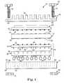
- FIG. 1is an exploded side elevational view of a printed circuit board (PCB) assembly in accordance with one embodiment of the present invention.
- PCBprinted circuit board
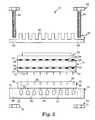
- FIG. 2is a side elevational view showing the components of the PCB ready for assembly.
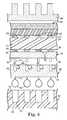
- FIG. 3is a partial, greatly enlarged side sectional view illustrating ready to be assembled electrical connection interfaces between a mother board, an electrical connector, a daughter card and a central processing unit (CPU) package of the PCB assembly in accordance with one embodiment of the present invention.
- CPUcentral processing unit
- FIG. 4is a side elevational view of the assembled PCB assembly.
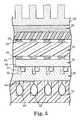
- FIG. 5is a partial, greatly enlarged side sectional view illustrating assembled electrical connection interfaces between the motherboard, the electrical connector, the daughter card and the CPU package of the PCB assembly in accordance with the one embodiment of present invention.
- FIGS. 1-5A printed circuit board (PCB) assembly 10 in accordance with the present invention is illustrated in FIGS. 1-5 .
- the PCB assembly 10includes a first PCB or motherboard 12 , a second PCB or daughter card 14 and an electrical connector 16 for electrically connecting the daughter card 14 to the motherboard 12 .
- the motherboard 12is defined by a first or upper major surface 18 , and an opposite second or lower major surface 20 .
- a plurality of conductive apertures 22i.e., electrical contacts
- the daughter card 14is defined by a first or upper major surface 24 , and an opposite second or lower major surface 26 .
- the upper major surface 24 of the daughter card 14includes a land grid array (LGA) defined by a plurality of electrical contact pads 28 .
- the lower major surface 26 of the daughter card 14also includes a LGA defined by a plurality of further electrical contact pads 30 .
- LGAland grid array
- a microprocessor central processing unit (CPU) package 25is adapted to be electrically coupled to the daughter card 14 .
- a lower surface 27 of the CPU package 25includes a ball grid array (BGA) defined by a plurality of electrical contact elements 29 .
- BGAball grid array
- the electrical contact elements 29 on the lower surface 27 of the CPU package 25are aligned with and soldered (in a known manner) to the electrical contact pads 28 on the upper surface 24 of the daughter card 14 .
- the electrical connector 16is defined by a first or lower connector component 32 and a second or upper connector component 34 .
- the lower connector component 32includes a nonconductive body 36 .
- the nonconductive bodyis molded of a suitable plastic material.
- the nonconductive body 36includes a first or upper side 38 and an opposite second or lower side 40 .
- a plurality of conductive apertures 42i.e., electrical contacts
- the lower connector component 32further includes a plurality of conductive pins 44 that extend outwardly from the lower side 40 of the nonconductive body 36 . As seen best in FIGS. 3 and 5 , a free end of each conductive pin 44 is formed in a loop end 46 .
- the plurality of conductive pins 44are aligned with and inserted into the conductive apertures 22 of the motherboard 12 .
- the loop ends 46 of the conductive pins 44flex inwardly (compare FIGS. 3 and 5 ) to form a releasable press fit (PF) interengagement between the conductive pins 44 of the lower connector component 32 and the conductive apertures 22 of the mother board 12 .
- the sides of the loop ends 46 of the conductive pins 44 of the lower connector component 32are placed in a mechanical shear or bind with the conductive apertures 22 of the mother board 12 to form a reliable electrical connection between the lower connector component 32 of the electrical connector 16 and the mother board 12 .
- the conductive pins 44 of the lower connector component 32With the conductive pins 44 of the lower connector component 32 fully inserted into the conductive apertures 22 of the mother board 12 , the lower side 40 of the nonconductive body 36 of the lower connector component 32 contacts and is supported by the upper major surface 18 of the mother board 12 .
- the upper connector component 34 of the electrical connector 16includes a first or upper side 48 and an opposite second or lower side 50 .
- the upper side 48 of the upper connector component 34includes a ball grid array (BGA) defined by a plurality of electrical contact elements 52 .
- a plurality of pin contacts 54extend outwardly from the lower side 50 of the upper connector component 34 of the electrical connector 16 .
- the electrical contact elements 52 on the upper side 48 of the upper connector component 34are aligned with and soldered (in a known manner) to the electrical contact pads 30 on the lower surface 26 of the daughter card 14 .
- the pin contacts 54can be formed integrally with the daughter card 14 so as to extend outwardly from the lower major surface 26 thereof.
- the plurality of pin contacts 54 of the upper connector component 34are aligned with and inserted into the conductive apertures 42 of the lower connector component 34 (see FIGS. 3 and 5 ).
- the pin contacts 54rotate cam members 56 in the conductive apertures 42 (compare FIGS. 3 and 5 ) to form a releasable zero insertion force (ZIF) interengagement between the pin contacts 54 of the upper connector component 34 and the conductive apertures 42 of the lower connector component 32 .
- ZIFzero insertion force
- the sides of the pin contacts 54 of the upper connector component 34are placed in a mechanical shear or bind with the conductive apertures 42 of the lower connector component 32 to form a reliable electrical connection between the upper connector component 34 of the electrical connector 16 and the lower connector component 32 of the electrical connector 16 , and thereby a reliable electrical connection between the daughter card 14 (with CPU package 25 ) and the mother board 12 .
- the PCB assembly 10 of the present inventionemploys a retention assembly 58 .
- the retention assembly 58includes a heat sink 60 , to remove heat generated by the motherboard 12 /daughter card 12 /CPU package 25 during operation, and a retention mechanism 62 .
- the heat sinkis positioned atop the CPU package 25 on the daughter card 14 .
- the retention mechanism 62acts between the heat sink 60 and the motherboard 12 to firmly secure the daughter card 14 (with CPU package 25 ) to the motherboard 12 .
- the daughter card 14(with CPU package 25 ) is in essence “sandwiched” between the heat sink 60 and the motherboard 12 and is held in place by the retention mechanism 62 .
- the weight of the heat sink 60 together with the clamping forces provided by the retention mechanism 62places the daughter card 14 , CPU package 25 and the electrical connector 16 under compression loading.
- the PF interengagement between the conductive pins 44 of the lower connector component 32 and the conductive apertures 22 of the mother board 12allows the lower side 40 of the nonconductive body 36 of the lower connector component 32 to contact and be supported by the upper major surface 18 of the mother board 12 , thereby virtually eliminating the deterioration of the electrical connection between the lower connector component 32 and the mother board 12 due to compression loading, power cycling and thermal cycling.
- the retention mechanism 62includes a plurality of threaded fasteners 64 that are adapted to freely pass through openings 66 in the heat sink 60 and openings 68 in the motherboard 12 . Nuts 70 are then threaded onto the threaded fasteners 64 to impart the above-described clamping forces and compression loading and to secure the daughter card 14 (With CPU package 25 ) to the motherboard 12 .
- other meanssuch as clamping levers could be used to provide the above described clamping forces and compression loading to secure the daughter card 14 (With CPU package 25 ) to the motherboard 12 .
- This PCB assembly 10provides a reliable electrical connection between the motherboard 12 and the daughter card 14 .
- the conductive pins 44 of the lower connector component 32being received by the conductive apertures 22 of the mother board 12 in a PF manner, allows the nonconductive body 36 of the lower connector component 32 to contact and be supported by the upper major surface 18 of the mother board 12 , thereby providing a reliable electrical connection that is not susceptible to deterioration as a result of compressive loads, thermal cycling and/or power cycling.
- the PCB assembly 10 of the present inventionis relatively easy and inexpensive to manufacture.
Landscapes
- Engineering & Computer Science (AREA)
- Microelectronics & Electronic Packaging (AREA)
- Coupling Device And Connection With Printed Circuit (AREA)
- Connecting Device With Holders (AREA)
Abstract
Description
Claims (15)
Priority Applications (2)
| Application Number | Priority Date | Filing Date | Title |
|---|---|---|---|
| US10/279,586US6903941B2 (en) | 2002-10-24 | 2002-10-24 | Printed circuit board assembly employing a press fit electrical connector |
| JP2003338641AJP2004146373A (en) | 2002-10-24 | 2003-09-29 | Printed circuit board assembly employing press fit electrical connector |
Applications Claiming Priority (1)
| Application Number | Priority Date | Filing Date | Title |
|---|---|---|---|
| US10/279,586US6903941B2 (en) | 2002-10-24 | 2002-10-24 | Printed circuit board assembly employing a press fit electrical connector |
Publications (2)
| Publication Number | Publication Date |
|---|---|
| US20040080921A1 US20040080921A1 (en) | 2004-04-29 |
| US6903941B2true US6903941B2 (en) | 2005-06-07 |
Family
ID=32106754
Family Applications (1)
| Application Number | Title | Priority Date | Filing Date |
|---|---|---|---|
| US10/279,586Expired - Fee RelatedUS6903941B2 (en) | 2002-10-24 | 2002-10-24 | Printed circuit board assembly employing a press fit electrical connector |
Country Status (2)
| Country | Link |
|---|---|
| US (1) | US6903941B2 (en) |
| JP (1) | JP2004146373A (en) |
Cited By (15)
| Publication number | Priority date | Publication date | Assignee | Title |
|---|---|---|---|---|
| US20060149883A1 (en)* | 2005-01-05 | 2006-07-06 | Benbow James B | Systems and methods for providing co-processors to computing systems |
| US20070278669A1 (en)* | 2006-05-31 | 2007-12-06 | Infineon Technologies Ag | Semiconductor circuit arrangement |
| US20080054430A1 (en)* | 2006-08-29 | 2008-03-06 | International Business Machines Corporation | Through board stacking of multiple LGA-connected components |
| US20080187636A1 (en)* | 1993-07-07 | 2008-08-07 | Jack Guttman, Inc. | Cake decorating with edible material printed with animage by an ink jet printer |
| US7438558B1 (en)* | 2007-11-13 | 2008-10-21 | International Business Machines Corporation | Three-dimensional stackable die configuration for an electronic circuit board |
| US7438557B1 (en) | 2007-11-13 | 2008-10-21 | International Business Machines Corporation | Stacked multiple electronic component interconnect structure |
| US20090034222A1 (en)* | 2007-08-01 | 2009-02-05 | Smith Mark W | Printed circuit board assembly and method of making a printed circuit board |
| US20090086443A1 (en)* | 2004-08-06 | 2009-04-02 | Claus Moessner | Interface module |
| US20090213552A1 (en)* | 2004-08-03 | 2009-08-27 | Infineon Technoligies Ag | Component arragement with an optimized assembly capability |
| US20100165582A1 (en)* | 2008-03-04 | 2010-07-01 | Infineon Technologies Ag | Power semiconductor module system |
| US20110085313A1 (en)* | 2009-10-14 | 2011-04-14 | International Business Machines Corporation | Motherboard Assembly for Interconnecting and Distributing Signals and Power |
| US20160360647A1 (en)* | 2015-06-04 | 2016-12-08 | Eaton Corporation | Ceramic plated materials for electrical isolation and thermal transfer |
| US20170315150A1 (en)* | 2015-02-05 | 2017-11-02 | Leeno Industrial Inc. | Test device |
| US10327356B2 (en)* | 2017-05-15 | 2019-06-18 | Fujitsu Limited | Electronic apparatus |
| WO2020087165A1 (en)* | 2018-11-01 | 2020-05-07 | Reflex Photonics Inc. | Heat dissipation from active devices connected to connectors |
Families Citing this family (7)
| Publication number | Priority date | Publication date | Assignee | Title |
|---|---|---|---|---|
| US6951466B2 (en)* | 2003-09-02 | 2005-10-04 | Hewlett-Packard Development Company, L.P. | Attachment plate for directly mating circuit boards |
| US7193300B2 (en)* | 2004-09-13 | 2007-03-20 | Honeywell International Inc. | Plastic leadframe and compliant fastener |
| DE102008001557A1 (en)* | 2008-05-05 | 2009-11-12 | Robert Bosch Gmbh | Male connector contacting via intermediate PCBs |
| US8287289B2 (en)* | 2008-06-10 | 2012-10-16 | Molex Incorporated | Elastic-cushioned capacitively-coupled connector |
| JP5113101B2 (en) | 2009-01-30 | 2013-01-09 | モレックス インコーポレイテド | Electrical circuit connection structure and electrical circuit connection method |
| JP6440315B2 (en)* | 2015-04-03 | 2018-12-19 | シチズン電子株式会社 | connector |
| US10741951B2 (en) | 2017-11-13 | 2020-08-11 | Te Connectivity Corporation | Socket connector assembly for an electronic package |
Citations (17)
| Publication number | Priority date | Publication date | Assignee | Title |
|---|---|---|---|---|
| US3676932A (en) | 1969-11-06 | 1972-07-18 | Charles F Druet | Device for the preparation of mixtures of liquids in pre-determined proportions and quantities |
| US4773873A (en) | 1986-10-01 | 1988-09-27 | Thinking Machines Corporation | Bistable zero insertion force connector |
| US4912401A (en)* | 1989-01-18 | 1990-03-27 | Tektronix, Inc. | Connection apparatus for interactively accessing an electronic device in a pin grid array socket |
| US5473510A (en)* | 1994-03-25 | 1995-12-05 | Convex Computer Corporation | Land grid array package/circuit board assemblies and methods for constructing the same |
| US5481435A (en)* | 1992-12-30 | 1996-01-02 | Interconnect Systems, Inc. | Adaptor assembly for adding functionality to a pin grid receptacle on a circuit board |
| US5547389A (en) | 1995-05-23 | 1996-08-20 | Hsu; Feng-Chien | Integrated circuit chip socket |
| US5707247A (en) | 1995-10-12 | 1998-01-13 | Intel Corporation | Low-profile zero-insertion force socket |
| US5772451A (en) | 1993-11-16 | 1998-06-30 | Form Factor, Inc. | Sockets for electronic components and methods of connecting to electronic components |
| US5842874A (en)* | 1994-05-25 | 1998-12-01 | Molex Incorporated | Dual housing board-to-board connector |
| US5893770A (en) | 1993-11-17 | 1999-04-13 | Dell Usa, L.P. | Retention member for zero insertion force socket |
| US5931689A (en)* | 1997-08-06 | 1999-08-03 | Molex Incorporated | Electric connector assembly with improved locking characteristics |
| US5982635A (en)* | 1996-10-23 | 1999-11-09 | Concept Manufacturing, Incorporated | Signal adaptor board for a pin grid array |
| US6004152A (en) | 1998-08-07 | 1999-12-21 | Hon Hai Precision Ind. Co., Ltd. | ZIF PGA socket |
| US6099321A (en) | 1998-09-04 | 2000-08-08 | Hon Hai Precision Ind. Co., Ltd. | Low profile zero insertion force socket |
| US6106316A (en) | 1999-02-10 | 2000-08-22 | International Business Machines Corporation | Multistage connector for carriers with combined pin-array and pad-array |
| US6186815B1 (en) | 1998-12-11 | 2001-02-13 | Hon Hai Precision Ind. Co., Ltd. | Zero insertion force socket |
| US6219241B1 (en) | 1999-06-11 | 2001-04-17 | Intel Coroporation | Advanced zero-insertion force (ZIF) socket with heat sink alignment and retention mechanisms |
- 2002
- 2002-10-24USUS10/279,586patent/US6903941B2/ennot_activeExpired - Fee Related
- 2003
- 2003-09-29JPJP2003338641Apatent/JP2004146373A/ennot_activeWithdrawn
Patent Citations (17)
| Publication number | Priority date | Publication date | Assignee | Title |
|---|---|---|---|---|
| US3676932A (en) | 1969-11-06 | 1972-07-18 | Charles F Druet | Device for the preparation of mixtures of liquids in pre-determined proportions and quantities |
| US4773873A (en) | 1986-10-01 | 1988-09-27 | Thinking Machines Corporation | Bistable zero insertion force connector |
| US4912401A (en)* | 1989-01-18 | 1990-03-27 | Tektronix, Inc. | Connection apparatus for interactively accessing an electronic device in a pin grid array socket |
| US5481435A (en)* | 1992-12-30 | 1996-01-02 | Interconnect Systems, Inc. | Adaptor assembly for adding functionality to a pin grid receptacle on a circuit board |
| US5772451A (en) | 1993-11-16 | 1998-06-30 | Form Factor, Inc. | Sockets for electronic components and methods of connecting to electronic components |
| US5893770A (en) | 1993-11-17 | 1999-04-13 | Dell Usa, L.P. | Retention member for zero insertion force socket |
| US5473510A (en)* | 1994-03-25 | 1995-12-05 | Convex Computer Corporation | Land grid array package/circuit board assemblies and methods for constructing the same |
| US5842874A (en)* | 1994-05-25 | 1998-12-01 | Molex Incorporated | Dual housing board-to-board connector |
| US5547389A (en) | 1995-05-23 | 1996-08-20 | Hsu; Feng-Chien | Integrated circuit chip socket |
| US5707247A (en) | 1995-10-12 | 1998-01-13 | Intel Corporation | Low-profile zero-insertion force socket |
| US5982635A (en)* | 1996-10-23 | 1999-11-09 | Concept Manufacturing, Incorporated | Signal adaptor board for a pin grid array |
| US5931689A (en)* | 1997-08-06 | 1999-08-03 | Molex Incorporated | Electric connector assembly with improved locking characteristics |
| US6004152A (en) | 1998-08-07 | 1999-12-21 | Hon Hai Precision Ind. Co., Ltd. | ZIF PGA socket |
| US6099321A (en) | 1998-09-04 | 2000-08-08 | Hon Hai Precision Ind. Co., Ltd. | Low profile zero insertion force socket |
| US6186815B1 (en) | 1998-12-11 | 2001-02-13 | Hon Hai Precision Ind. Co., Ltd. | Zero insertion force socket |
| US6106316A (en) | 1999-02-10 | 2000-08-22 | International Business Machines Corporation | Multistage connector for carriers with combined pin-array and pad-array |
| US6219241B1 (en) | 1999-06-11 | 2001-04-17 | Intel Coroporation | Advanced zero-insertion force (ZIF) socket with heat sink alignment and retention mechanisms |
Cited By (31)
| Publication number | Priority date | Publication date | Assignee | Title |
|---|---|---|---|---|
| US20080187636A1 (en)* | 1993-07-07 | 2008-08-07 | Jack Guttman, Inc. | Cake decorating with edible material printed with animage by an ink jet printer |
| US20090213552A1 (en)* | 2004-08-03 | 2009-08-27 | Infineon Technoligies Ag | Component arragement with an optimized assembly capability |
| US8089768B2 (en)* | 2004-08-03 | 2012-01-03 | Infineon Technologies Ag | Component arragement with an optimized assembly capability |
| US8908385B2 (en)* | 2004-08-06 | 2014-12-09 | Robert Bosch Gmbh | Interface module |
| US20090086443A1 (en)* | 2004-08-06 | 2009-04-02 | Claus Moessner | Interface module |
| US20060149883A1 (en)* | 2005-01-05 | 2006-07-06 | Benbow James B | Systems and methods for providing co-processors to computing systems |
| US7454550B2 (en)* | 2005-01-05 | 2008-11-18 | Xtremedata, Inc. | Systems and methods for providing co-processors to computing systems |
| US20070278669A1 (en)* | 2006-05-31 | 2007-12-06 | Infineon Technologies Ag | Semiconductor circuit arrangement |
| US7708584B2 (en)* | 2006-05-31 | 2010-05-04 | Infineon Technologies Ag | Semiconductor circuit arrangement |
| US8278745B2 (en) | 2006-08-29 | 2012-10-02 | International Business Machines Corporation | Through board stacking of multiple LGA-connected components |
| US20090315168A1 (en)* | 2006-08-29 | 2009-12-24 | International Business Machines Corporation | Through board stacking of multiple lga-connected components |
| US20080054430A1 (en)* | 2006-08-29 | 2008-03-06 | International Business Machines Corporation | Through board stacking of multiple LGA-connected components |
| US8174106B2 (en)* | 2006-08-29 | 2012-05-08 | International Business Machines Corporation | Through board stacking of multiple LGA-connected components |
| US20090034222A1 (en)* | 2007-08-01 | 2009-02-05 | Smith Mark W | Printed circuit board assembly and method of making a printed circuit board |
| US7864544B2 (en) | 2007-08-01 | 2011-01-04 | Delphi Technologies, Inc. | Printed circuit board assembly |
| US20090119902A1 (en)* | 2007-11-13 | 2009-05-14 | International Business Machines Corporation | Stacked multiple electronic component interconnect structure |
| US7534111B1 (en) | 2007-11-13 | 2009-05-19 | International Business Machines Corporation | Stacked multiple electronic component interconnect structure |
| US20090119911A1 (en)* | 2007-11-13 | 2009-05-14 | International Business Machines Corporation | Forming a three-dimensional stackable die configuration for an electronic circuit board |
| US7438558B1 (en)* | 2007-11-13 | 2008-10-21 | International Business Machines Corporation | Three-dimensional stackable die configuration for an electronic circuit board |
| US7438557B1 (en) | 2007-11-13 | 2008-10-21 | International Business Machines Corporation | Stacked multiple electronic component interconnect structure |
| US8238108B2 (en)* | 2008-03-04 | 2012-08-07 | Infineon Technologies Ag | Power semiconductor module system |
| US20100165582A1 (en)* | 2008-03-04 | 2010-07-01 | Infineon Technologies Ag | Power semiconductor module system |
| US20110085313A1 (en)* | 2009-10-14 | 2011-04-14 | International Business Machines Corporation | Motherboard Assembly for Interconnecting and Distributing Signals and Power |
| US8446738B2 (en) | 2009-10-14 | 2013-05-21 | International Business Machines Corporation | Motherboard assembly for interconnecting and distributing signals and power |
| US8958214B2 (en) | 2009-10-14 | 2015-02-17 | International Business Machines Corporation | Motherboard assembly for interconnecting and distributing signals and power |
| US20170315150A1 (en)* | 2015-02-05 | 2017-11-02 | Leeno Industrial Inc. | Test device |
| US10302674B2 (en)* | 2015-02-05 | 2019-05-28 | Leeno Industrial Inc. | Test device |
| US20160360647A1 (en)* | 2015-06-04 | 2016-12-08 | Eaton Corporation | Ceramic plated materials for electrical isolation and thermal transfer |
| US10629513B2 (en)* | 2015-06-04 | 2020-04-21 | Eaton Intelligent Power Limited | Ceramic plated materials for electrical isolation and thermal transfer |
| US10327356B2 (en)* | 2017-05-15 | 2019-06-18 | Fujitsu Limited | Electronic apparatus |
| WO2020087165A1 (en)* | 2018-11-01 | 2020-05-07 | Reflex Photonics Inc. | Heat dissipation from active devices connected to connectors |
Also Published As
| Publication number | Publication date |
|---|---|
| US20040080921A1 (en) | 2004-04-29 |
| JP2004146373A (en) | 2004-05-20 |
Similar Documents
| Publication | Publication Date | Title |
|---|---|---|
| US6903941B2 (en) | Printed circuit board assembly employing a press fit electrical connector | |
| US5761036A (en) | Socket assembly for electrical component | |
| US6178629B1 (en) | Method of utilizing a replaceable chip module | |
| EP0980594B1 (en) | Multi-mode compliant connector and replaceable chip module utilizing the same | |
| US6477058B1 (en) | Integrated circuit device package including multiple stacked components | |
| US6545226B2 (en) | Printed wiring board interposer sub-assembly | |
| US6231353B1 (en) | Electrical connector with multiple modes of compliance | |
| JP2001522135A (en) | Converter socket terminal | |
| JPH08321367A (en) | Low atittude socket type integrated circuit packaging system | |
| US6164978A (en) | Land grid array connector | |
| US20040111876A1 (en) | Reworking device for removing electrical elements mounted on motherboard | |
| US7341460B1 (en) | Electrical connector | |
| US5950072A (en) | Low-profile removable ball-grid-array integrated circuit package | |
| US7001190B2 (en) | Repairable ball grid array contact | |
| US6764313B2 (en) | High density interconnects | |
| US6644985B2 (en) | Ball attached zero insertion force socket | |
| JP2006210343A (en) | Compression load-adapted socket | |
| US6634891B1 (en) | Reworking device for removing electrical elements mounted on motherboard | |
| US20030150645A1 (en) | Method and apparatus for coupling a microelectronic device package to a circuit board | |
| US7177142B2 (en) | Hybrid compression socket connector for integrated circuits | |
| US7057295B2 (en) | IC module assembly | |
| US6493238B1 (en) | Method and apparatus to compliantly interconnect area grid arrays and printed wiring boards | |
| US6729896B2 (en) | Electrical connector with distortion-resistant cover | |
| CN1988756A (en) | Substrate structure, substrate manufacturing method and electronic device | |
| US6817878B2 (en) | Zero mounting force solder-free connector/component and method |
Legal Events
| Date | Code | Title | Description |
|---|---|---|---|
| AS | Assignment | Owner name:HEWLETT-PACKARD COMPANY, COLORADO Free format text:ASSIGNMENT OF ASSIGNORS INTEREST;ASSIGNOR:PAOLA, JOSE PIETRI;REEL/FRAME:013723/0929 Effective date:20021022 | |
| AS | Assignment | Owner name:HEWLETT-PACKARD DEVELOPMENT COMPANY, L.P., COLORADO Free format text:ASSIGNMENT OF ASSIGNORS INTEREST;ASSIGNOR:HEWLETT-PACKARD COMPANY;REEL/FRAME:013776/0928 Effective date:20030131 Owner name:HEWLETT-PACKARD DEVELOPMENT COMPANY, L.P., COLORAD Free format text:ASSIGNMENT OF ASSIGNORS INTEREST;ASSIGNOR:HEWLETT-PACKARD COMPANY;REEL/FRAME:013776/0928 Effective date:20030131 Owner name:HEWLETT-PACKARD DEVELOPMENT COMPANY, L.P.,COLORADO Free format text:ASSIGNMENT OF ASSIGNORS INTEREST;ASSIGNOR:HEWLETT-PACKARD COMPANY;REEL/FRAME:013776/0928 Effective date:20030131 | |
| FPAY | Fee payment | Year of fee payment:4 | |
| FPAY | Fee payment | Year of fee payment:8 | |
| AS | Assignment | Owner name:HEWLETT PACKARD ENTERPRISE DEVELOPMENT LP, TEXAS Free format text:ASSIGNMENT OF ASSIGNORS INTEREST;ASSIGNOR:HEWLETT-PACKARD DEVELOPMENT COMPANY, L.P.;REEL/FRAME:037079/0001 Effective date:20151027 | |
| REMI | Maintenance fee reminder mailed | ||
| LAPS | Lapse for failure to pay maintenance fees | ||
| STCH | Information on status: patent discontinuation | Free format text:PATENT EXPIRED DUE TO NONPAYMENT OF MAINTENANCE FEES UNDER 37 CFR 1.362 | |
| FP | Lapsed due to failure to pay maintenance fee | Effective date:20170607 |