US6903633B2 - Electronic tunable filters with dielectric varactors - Google Patents
Electronic tunable filters with dielectric varactorsDownload PDFInfo
- Publication number
- US6903633B2 US6903633B2US10/682,650US68265003AUS6903633B2US 6903633 B2US6903633 B2US 6903633B2US 68265003 AUS68265003 AUS 68265003AUS 6903633 B2US6903633 B2US 6903633B2
- Authority
- US
- United States
- Prior art keywords
- electrode
- radio frequency
- filter according
- frequency filter
- tunable dielectric
- Prior art date
- Legal status (The legal status is an assumption and is not a legal conclusion. Google has not performed a legal analysis and makes no representation as to the accuracy of the status listed.)
- Expired - Lifetime
Links
Images


Classifications
- H—ELECTRICITY
- H01—ELECTRIC ELEMENTS
- H01P—WAVEGUIDES; RESONATORS, LINES, OR OTHER DEVICES OF THE WAVEGUIDE TYPE
- H01P1/00—Auxiliary devices
- H01P1/20—Frequency-selective devices, e.g. filters
- H01P1/201—Filters for transverse electromagnetic waves
- H01P1/203—Strip line filters
- H01P1/20327—Electromagnetic interstage coupling
- H01P1/20336—Comb or interdigital filters
- H—ELECTRICITY
- H01—ELECTRIC ELEMENTS
- H01P—WAVEGUIDES; RESONATORS, LINES, OR OTHER DEVICES OF THE WAVEGUIDE TYPE
- H01P1/00—Auxiliary devices
- H01P1/20—Frequency-selective devices, e.g. filters
- H01P1/201—Filters for transverse electromagnetic waves
- H01P1/203—Strip line filters
- H01P1/20327—Electromagnetic interstage coupling
- H01P1/20354—Non-comb or non-interdigital filters
- H01P1/20381—Special shape resonators
- H—ELECTRICITY
- H01—ELECTRIC ELEMENTS
- H01P—WAVEGUIDES; RESONATORS, LINES, OR OTHER DEVICES OF THE WAVEGUIDE TYPE
- H01P1/00—Auxiliary devices
- H01P1/20—Frequency-selective devices, e.g. filters
- H01P1/201—Filters for transverse electromagnetic waves
- H01P1/205—Comb or interdigital filters; Cascaded coaxial cavities
- H01P1/2056—Comb filters or interdigital filters with metallised resonator holes in a dielectric block
Definitions
- the present inventiongenerally relates to electronic filters and, more particularly, to such filters that include tunable dielectric capacitors (dielectric varactors).
- Electrically tunable filtersare suitable for mobile and portable communication applications, compared to other tunable filters such as mechanically and magnetically tunable filters. Both mechanically and magnetically tunable filters are relatively large in size and heavy in weight. Electronically tunable filters have the important advantages of small size, lightweight, low power consumption, simple control circuits, and fast tuning capability. Electronically tunable filters can be divided into two types: one is tuned by tunable dielectric capacitors (dielectric varactors), and the other is tuned by semiconductor diode varactors.
- the dielectric varactoris a voltage tunable capacitor in which the dielectric constant of a dielectric material in the capacitor can be changed by a voltage applied thereto.
- dielectric varactorsCompared to semiconductor diode varactors, dielectric varactors have the merits of lower loss, higher power-handling, higher IP 3 , and faster tuning speed.
- Third intermodulation distortionhappens when two close frequency signals (f 1 and f 2 ) are input into a filter. The two signals generate two related signals at frequencies of 2f 2 ⁇ f 1 (say f 3 ), and 2f 1 ⁇ f 2 (say f 4 ), in addition to the two main signals f 1 and f 2 .
- F 3 and f 4should be as low as possible compared to f 1 and f 2 .
- the relationship between f 1 , f 2 , f 3 and f 4is characterized by IP 3 . The higher the IP 3 value is, the lower the third intermodulation.
- dielectric varactorsare suitable for tunable filters in mobile and portable communication applications.
- Tunable ferroelectric materialsare materials whose permittivity (more commonly called dielectric constant) can be varied by varying the strength of an electric field to which the materials are subjected. Even though these materials work in their paraelectric phase above the Curie temperature, they are conveniently called “ferroelectric” because they exhibit spontaneous polarization at temperatures below the Curie temperature. Tunable ferroelectric materials including barium-strontium titanate (BST) or BST composites have been the subject of several patents.
- BSTbarium-strontium titanate
- Dielectric materials including barium strontium titanateare disclosed in U.S. Pat. No. 5,312,790 to Sengupta, et al. entitled “Ceramic Ferroelectric Material”; U.S. Pat. No. 5,427,988 to Sengupta, et al. entitled “Ceramic Ferroelectric Composite Material—BSTO—MgO”; U.S. Pat. No. 5,486,491 to Sengupta, et al. entitled “Ceramic Ferroelectric Composite Material—BSTO—ZrO 2 ”; U.S. Pat. No. 5,635,434 to Sengupta, et al. entitled “Ceramic Ferroelectric Composite Material—BSTO-Magnesium Based Compound”; U.S.
- Radio frequency electronic filters constructed in accordance with this inventioninclude an input, an output, and first and second resonators coupled to the input and the output, with the first resonator including a first tunable dielectric varactor and the second resonator including a second tunable dielectric varactor.
- the resonatorscan take the form of a lumped element resonator, a ceramic resonator, or a microstrip resonator. Additional tunable dielectric varactors can be connected between the input and the first resonator and between the second resonator and the output. Tunable dielectric varactors can also be connected between the first and second resonators. Further embodiments include additional resonators and additional tunable dielectric varactors.
- the compact tunable filters of this inventionare suitable for mobile and portable communication applications such as handset phones.
- the high Q dielectric varactors used in the preferred embodiments of the inventionutilize low loss tunable thin film dielectric materials.
- FIG. 1is a schematic diagram of a lumped element LC tunable filter constructed in accordance with one embodiment of the invention
- FIG. 2is a schematic diagram of a DC bias circuit for varactors used in the filters of this invention
- FIG. 3is a schematic diagram of another lumped element LC tunable filter constructed in accordance with the invention.
- FIG. 4is a schematic diagram of another lumped element LC tunable filter constructed in accordance with the invention.
- FIG. 5is a plan view of a varactor that can be used in filters constructed in accordance with the present invention.
- FIG. 6is a sectional view of the varactor of FIG. 5 taken along line 6 — 6 ;
- FIG. 7is a plan view of another varactor that can be used in filters constructed in accordance with the present invention.
- FIG. 8is a sectional view of the varactor of FIG. 7 taken along line 8 — 8 ;
- FIG. 9is a plan view of another varactor that can be used in filters constructed in accordance with the present invention.
- FIG. 10is a sectional view of the varactor of FIG. 9 taken along line 10 — 10 ;
- FIG. 11is a plan view of another varactor that can be used in filters constructed in accordance with the present invention.
- FIG. 12is a sectional view of the varactor of FIG. 11 taken along line 12 — 12 ;
- FIG. 13is a plan view of another varactor that can be used in filters constructed in accordance with the present invention.
- FIG. 14is a sectional view of the varactor of FIG. 13 taken along line 14 — 14 ;
- FIG. 15is a plan view of another varactor that can be used in filters constructed in accordance with the present invention.
- FIG. 16is a sectional view of the varactor of FIG. 15 taken along line 16 — 16 ;
- FIG. 17is an isometric view of a prior art ceramic filter that can be modified to include tunable varactors in accordance with the present invention
- FIG. 18is a longitudinal vertical cross sectional view of the filter of FIG. 17 ;
- FIG. 19is a top plan view of ceramic filter with a schematically illustrated varactor constructed in accordance with the present invention.
- FIG. 20is a schematic diagram of the filter of FIG. 19 ;
- FIG. 21is a top plan view of another ceramic filter with a schematically illustrated varactor constructed in accordance with the present invention.
- FIG. 22is a top plan view of another ceramic filter with a schematically illustrated varactor constructed in accordance with the present invention.
- FIG. 23is a schematic representation of a combline filter constructed in accordance with the present invention.
- FIGS. 24 , 25 , 26 and 27are schematic representations of additional combline filters constructed in accordance with the present invention.
- FIGS. 28 and 29are schematic diagrams of other lumped element LC tunable filters constructed in accordance with the invention.
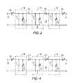
- FIG. 1is a schematic diagram of a three pole lumped element LC tunable filter 10 constructed in accordance with one embodiment of the invention.
- the filterincludes an input 12 and an output 14 .
- a plurality of resonant circuits 16 , 18 and 20are electrically coupled to the input and the output.
- Resonant circuit 16includes inductor L 1 and capacitor C 1 .
- Resonant circuit 18includes inductor L 2 and capacitor C 2 .
- Resonant circuit 20includes inductor L 3 and capacitor C 3 .
- Capacitor C 4couples resonant circuit 16 to the input 12 .
- Capacitor C 5couples resonant circuit 16 to resonant circuit 18 .
- Capacitor C 6couples resonant circuit 18 to resonant circuit 20 .
- Capacitor C 7couples resonant circuit 20 to the output 14 .
- Capacitors C 1 , C 2 and C 3are tunable dielectric varactors.
- C 4 and C 7are port coupling capacitors used to provide a specific port impedance, typically 50 ohms or 75 ohms. More or fewer resonators can be used in the filter to obtain specific filter rejection.
- Each of the tunable varactorsis connected to a voltage bias circuit not shown in FIG. 1 , but shown in FIG. 2 as bias circuit 22 .
- FIG. 2shows a voltage source 24 connected to varactor C 1 through an inductor 26 .
- a blocking capacitor 28is electrically connected in series with the varactor. By varying the voltage supplied by source 24 , the capacitance of the varactor changes. This enables tuning of the filter.
- the DC blocking capacitoris used to prevent the DC bias voltage from entering into the other parts of the filter.
- Inductor 26works as an RF choke to prevent RF signal leaking into the bias circuit.
- FIG. 3is a schematic diagram of another lumped element LC tunable filter 30 constructed in accordance with the invention.
- Filter 30is similar to filter 10 of FIG. 1 , except that capacitors fixed C 4 and C 7 in FIG. 1 have been replaced by varactors C 8 and C 9 in FIG. 3 .
- FIG. 4is a schematic diagram of another lumped element LC tunable filter 32 constructed in accordance with the invention.
- Filter 32is similar to filter 30 of FIG. 3 , except that capacitors fixed C 5 and C 6 in FIG. 3 have been replaced by varactors C 10 and C 11 in FIG. 4 .
- the lumped element tunable filters of FIGS. 1-4are particularly applicable for use in mobile and portable communications.
- Lumped element tunable filtershave the advantages of small size, simple structure, and low cost.
- the fixed resonating capacitors in a conventional LC lumped element filterare replaced by dielectric varactors.
- the tuning range of the filteris determined by the tuning range of the varactors.
- the coupling between resonators and resonator-portsmay be tunable.
- varactorsmay replace the fixed port coupling capacitors, as shown in FIGS. 3 and 4 .
- the lumped element tunable filter of FIG. 4shows a fully controlled filter for controlling center frequency, bandwidth, and return loss in the tuning range. Since each capacitance in the filter is tunable, the lumped element tunable filter of FIG. 4 has the highest tuning range compared to other tunable filters for a certain varactor tuning range. However, LC lumped element filters suffer from high insertion losses, and frequency limitations caused by lumped element behaviors vs. frequency.
- each of the filtersincludes varactors comprising a substrate, a first conductor positioned on a surface of the substrate, a second conductor positioned on the surface of the substrate and forming a gap between the first and second conductors, a tunable dielectric material positioned on the surface of the substrate and within the gap, the tunable dielectric material having a top surface, with at least a portion of said top surface being positioned above the gap opposite the surface of the substrate, and a first portion of the second conductor extending along at least a portion of the top surface of the tunable dielectric material.
- the second conductorcan overlap or not overlap a portion of the first conductor.
- FIGS. 5 and 6are top plan and cross-sectional views of a varactor 60 that can be used in filters constructed in accordance with the present invention.
- the varactorincludes a substrate 62 and a first electrode 64 positioned on first portion 66 of a surface 68 of the substrate.
- a second electrode 70is positioned on second portion 72 of the surface 68 of the substrate and separated from the first electrode to form a gap 74 therebetween.
- a tunable dielectric material 76is positioned on the surface 68 of the substrate and in the gap between the first and second electrodes.
- a section 78 of the tunable dielectric material 76extends along a surface 80 of the first electrode 64 opposite the substrate.
- the second electrode 70includes a projection 82 that is positioned on a top surface 84 of the tunable dielectric layer opposite the substrate.
- projection 82has a rectangular shape and extends along the top surface 84 such that it vertically overlaps a portion 86 of the first electrode.
- the second electrodecan be referred to as a “T-type” electrode.
- a DC bias voltageas illustrated by voltage source 88 , is applied to the electrodes 64 and 70 to control the dielectric constant of the tunable dielectric material lying between the electrodes 64 and 70 .
- An input 90is provided for receiving an electrical signal and an output 92 is provided for delivering the signal.
- the tunable dielectric layer 76can be a thin or thick film.
- the horizontal distance (HD) along the surface of the substrate between the first and second electrodesis much greater than the thickness (t) of the dielectric film.
- thickness of tunable filmis ⁇ 1 micrometer for thin films, and ⁇ 5 micrometers for thick film, and the horizontal distance is greater than 50 micrometers.
- the horizontal distancemainly depends on the processing used to fabricate the device, and is typically about >50 micrometers. In practice, we choose HD>10t.
- the substrate layer 62may be comprised of MgO, alumina (Al 2 O 3), LaAlO 3 , sapphire, quartz, silicon, gallium arsenide, and other materials that are compatible with the various tunable films and the electrodes, as well as the processing used to produce the tunable films and the electrodes.
- the bottom electrode 64can be deposited on the surface of the substrate by electron-beam, sputtering, electroplating or other metal film deposition techniques.
- the bottom electrodepartially covers the substrate surface, which is typically done by etching processing.
- the thickness of the bottom electrodein one preferred embodiment is about 2 ⁇ m.
- the bottom electrodeshould be compatible with the substrate and the tunable films, and should be able to withstand the film processing temperature.
- the bottom electrodemay typically be comprised of platinum, platinum-rhodium, ruthenium oxide or other materials that are compatible with the substrate and tunable films, as well as with the film processing.
- Another filmmay be required between the substrate and bottom electrode as an adhesion layer, or buffer layer for some cases, for example platinum on silicon can use a layer of silicon oxide, titanium or titanium oxide as a buffer layer.
- the thin or thick film of tunable dielectric material 76is then deposited on the bottom electrode and the rest of the substrate surface by techniques such as metal-organic solution deposition (MOSD or simply MOD), metal-organic chemical vapor deposition (MOCVD), pulse laser deposition (PLD), sputtering, screen printing and so on.
- MOSDmetal-organic solution deposition
- MOCVDmetal-organic chemical vapor deposition
- PLDpulse laser deposition
- sputteringscreen printing and so on.
- the thickness of the thin or thick film that lies above the bottom electrodeis preferably in range of 0.2 ⁇ m to 4 ⁇ m. It is well known that the performance of a varactor depends on the quality of the tunable dielectric film. Therefore low loss and high tunability films should be selected to achieve high Q and high tuning of the varactor.
- these tunable dielectric filmshave dielectric constants of 2 to 1000, and tuning of greater than 20% with a loss tangent less than 0.005 at around 2 GHz.
- low dielectric constant (k) filmsshould be selected.
- high k filmsusually shows high tunability. The typical k range is about 100 to 500.
- the tunable dielectric layeris preferably comprised of Barium-Strontium Titanate, Ba x Sr 1-x TiO 3 (BSTO), where x can range from zero to one, or BSTO-composite ceramics.
- BSTO compositesinclude, but are not limited to: BSTO—MgO, BSTO—MgAl 2 O 4 , BSTO—CaTiO 3 , BSTO—MgTiO 3 , BSTO—MgSrZrTiO 6 , and combinations thereof.
- Other tunable dielectric materialsmay be used partially or entirely in place of barium strontium titanate.
- An exampleis Ba x Ca 1-x TiO 3 , where x ranges from 0.2 to 0.8, and preferably from 0.4 to 0.6.
- Additional alternative tunable ferroelectricsinclude Pb x Zr 1-x TiO 3 (PZT) where x ranges from 0.05 to 0.4, lead lanthanum zirconium titanate (PLZT), lead titanate (PbTiO 3 ), barium calcium zirconium titanate (BaCaZrTiO 3 ), sodium nitrate (NaNO 3 ), KNbO 3 , LiNbO 3 , LiTaO 3 , PbNb 2 O 6 , PbTa 2 O 6 , KSr(NbO 3 ), and NaBa 2 (NbO 3 ) 5 and KH 2 PO 4 .
- the second electrode 70is formed by a conducting material deposited on the surface of the substrate and at least partially overlapping the tunable film, by using similar processing as set forth above for the bottom electrode.
- Metal etching processingcan be used to achieve specific top electrode patterns. The etching processing may be dry or wet etching.
- the top electrode materialscan be gold, silver, copper, platinum, ruthenium oxide or other conducting materials that are compatible with the tunable films. Similar to the bottom electrode, a buffer layer for the top electrode could be necessary, depending on electrode-tunable film system. Finally, a part of the tunable film should be etched away to expose the bottom electrode.
- the pattern and arrangement of the top electrodeare key parameters in determining the capacitance of the varactor.
- the top electrodemay have a small overlap (as shown in FIGS. 5 and 6 ) or no overlap with the bottom electrode.
- FIGS. 7 and 8are top plan and cross-sectional views of a varactor 94 , that can be used in filters of the invention, having a T-type top electrode with no overlap electrode area.
- the structural elements of the varactor of FIGS. 7 and 8are similar to the varactor of FIGS. 5 and 6 , except that the rectangular projection 96 on electrode 98 is smaller and does not overlap electrode 64 . Varactors with no electrode overlap area may need more tuning voltage than those in which the electrodes overlap.
- FIGS. 9 and 10are top plan and cross-sectional views of a varactor 100 , that can be used in filters of the invention, having a top electrode 102 with a trapezoid-type projection 106 and an overlapped electrode area 104 .
- the structural elements of the varactor of FIGS. 9 and 10are similar to the varactor of FIGS. 5 and 6 , except that the projection 106 on electrode 102 has a trapezoidal shape. Since the projection on the T-type electrode of the varactor of FIGS. 5 and 6 is relatively narrow, the trapezoid-type top electrode of the varactor of FIGS. 9 and 10 is less likely to break, compared to the T-type pattern varactor.
- FIGS. 11 and 12are top plan and cross-sectional views of a varactor 108 having a trapezoid-type electrode 110 having a smaller projection 112 with no overlap area of electrodes to obtain lower capacitance.
- FIGS. 13 and 14are top plan and cross-sectional views of a varactor 114 , that can be used in filters of the invention, having triangle-type projection 116 on the top electrode 118 that overlaps a portion of the bottom electrode at region 120 . Using a triangle projection on the top electrode may make it easier to reduce the overlap area of electrodes.
- FIGS. 15 and 16are top plan and cross-sectional views of a varactor 122 having triangle-type projection 124 on the top electrode 126 that does not overlap the bottom electrode.
- the inventionuses voltage tunable thick film and thin film varactors that can be used in room temperature.
- Vertical structure dielectric varactors with specific electrode patterns and arrangements as described aboveare used to achieve low capacitance in the present invention.
- Variable overlap and no overlap structures of the bottom and top electrodesare designed to limit effective area of the vertical capacitor.
- Low loss and high tunability thin and thick filmsare used to improve performance of the varactors. Combined with the low loss and high tunability materials, the varactors have low capacitance, higher Q, high tuning, and low bias voltage.
- FIG. 17is an isometric view of a prior art ceramic filter 130 that can be modified to include tunable varactors in accordance with the present invention.
- FIG. 18is a longitudinal vertical cross sectional view of the filter of FIG. 17 .
- Filter 130includes an input 132 and an output 134 , each coupled to a block 136 of ceramic material.
- the ceramic blockincludes a plurality of openings 138 , 140 , 142 , 144 , 146 and 148 , extending from its top surface to its bottom surface with each hole lined by a metal tube 150 , 152 , 154 , 156 , 158 and 160 .
- the dielectric blockis covered with a conductive material 162 with the exception of portions near one end of each hole and near the first and second electrodes. Slots 164 , 166 , 168 , 170 and 172 are cut into the sides of the conductive material and the ceramic block. Tabs 174 and 176 are used to connect the ceramic block to the input and output connector
- FIG. 19is a top plan view of ceramic filter 178 with a schematically illustrated varactor constructed in accordance with the present invention.
- the filter 178includes a metallic housing 180 that holds a ceramic block 182 . Holes 184 , 186 and 188 are positioned in the ceramic block 182 .
- Metallic tubes 190 , 192 and 194line the holes.
- Dielectric varactors 196 , 198 and 200couple tubes 190 , 192 and 194 respectively, to the housing.
- Projections 202 , 204 , 206 and 208extend from the housing into the ceramic block. Tabs 210 and 212 are used to connect the input and output of the filter to an external circuit.
- FIG. 20is a schematic diagram of the filter of FIG. 19 .
- the filteris shown to include three resonant circuits 214 , 216 and 218 .
- the resonant circuitsare coupled by inductors L 4 and L 5 .
- Dielectric varactors C 12 , C 13 and C 14are electrically connected in parallel with resonant circuits 214 , 216 and 218 , respectively.
- Capacitor C 15couples the input 220 to the first resonant circuit 214 .
- Capacitor C 16couples the output 222 to the third resonant circuit 218 . Since the capacitance contributed by the dielectric varactors is a part of the capacitance in each resonator, tuning of varactor can tune the resonating frequency.
- FIG. 21is a top plan view of another ceramic filter 224 with schematically illustrated varactors constructed in accordance with the present invention.
- the filter of FIG. 21is similar to that of FIG. 19 , with the addition of dielectric varactors 226 and 228 .
- Dielectric varactor 226couples tube 190 to the input tab 210 and dielectric varactor 228 couples tube 194 to the output tab 212 .
- FIG. 22is a top plan view of another ceramic filter 230 with schematically illustrated varactors constructed in accordance with the present invention.
- the filter of FIG. 22is similar to that of FIG. 21 , with the addition of dielectric varactors 232 and 234 .
- Dielectric varactor 232couples tube 190 to the tube 192 and dielectric varactor 228 couples tube 192 to tube 194 .
- This tunable ceramic tunable filtershould have low insertion loss, compact size, and low cost. It should be noted that the ceramic filters of this invention are not limited to those shown in FIGS. 19 , 21 and 22 . Any fixed ceramic filters can be modified into tunable filters, as long as the dielectric varactors can be shunted between the resonating hole and its ground plane.
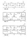
- FIG. 23is a schematic representation of a microstrip combline filter 236 constructed in accordance with the present invention.
- Filter 236includes an input 238 and an output 240 .
- a plurality of resonatorsare formed by microstrips 242 , 244 , 246 and 248 .
- Each resonatoris comprised of a microstrip line, a capacitor, and two short-circuited ends.
- Dielectric varactors 250 , 252 , 254 and 256connect the microstrips to ground.
- the bias circuit for each varactoris not shown for clarity, but would be similar to that for LC lumped element tunable filter as shown in FIG. 2 .
- FIGS. 24 , 25 , 26 and 27are schematic representations of additional combline filters constructed in accordance with the present invention.
- FIG. 24is a top plan view of another ceramic filter 260 with schematically illustrated varactors constructed in accordance with the present invention.
- the filter of FIG. 24is similar to that of FIG. 23 , with the addition of dielectric varactors 262 and 264 .
- Dielectric varactor 262couples microstrip 242 to the input 238 and dielectric varactor 264 couples microstrip 248 to the output 240 .
- FIG. 25is a top plan view of another ceramic filter 266 with schematically illustrated varactors constructed in accordance with the present invention.
- the filter of FIG. 25is similar to that of FIG. 24 , with the addition of dielectric varactors 268 , 270 and 272 .
- Dielectric varactor 268couples microstrip 242 to microstrip 244
- dielectric varactor 270couples microstrip 244 to microstrip 242
- dielectric varactor 272couples microstrip 246 to microstrip 242 .
- FIG. 26is a top plan view of another ceramic filter 274 with schematically illustrated varactors constructed in accordance with the present invention.
- Filer 274is similar to that shown in FIG. 23 , except for the use of transformer coupled input 276 and output 278 .
- FIG. 27is a top plan view of another ceramic filter 280 with schematically illustrated varactors constructed in accordance with the present invention.
- Filer 280is similar to that shown in FIG. 24 , except for the connection points for dielectric varactors 282 and 284 .
- the port couplingscan be tunable, as shown in FIG. 24 , as well as resonator coupling (FIG. 25 ), to improve filter performance in tuning range. It should be also noted that the invention is not limited to tapped combline filters as shown in FIG. 23 , but encompasses transformer, capacitive loaded, and others combline filters, shown in FIGS. 24 , 25 , 26 and 27 .
- Tunable filters with ceramic filters, combline filters, and LC-lumped element filtersare disclosed as examples of the dielectric varactor applications.
- the dielectric varactorsmay be located in resonators and/or in couplings in the filters to make filter tunable and to optimize performance of the filter during tuning processing.
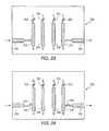
- resonators 286 , and 290are coupled to input 292 and output 294 .
- Resonator 286includes the parallel connection of varactor 296 and inductor 298 .
- Resonator 288includes the parallel connection of varactor 300 and inductor 302 .
- Resonator 290includes the parallel connection of varactor 304 and inductor 306 .
- Resonators 286 and 288are coupled to each other by a series circuit including inductor 308 and capacitor 310 .
- Resonators 288 and 290are coupled to each other by a series circuit including inductor 312 and capacitor 314 .
- the filter of FIG. 29is similar to that of FIG. 28 except that the resonators 286 and 288 are coupled by a parallel connection of inductor 316 and capacitor 318 , and resonators 288 and 290 are coupled by a parallel connection of inductor 320 and capacitor 322 .
- resonator 286is coupled to the input be capacitor 324 and resonator 290 is coupled to the output by capacitor 326 .
- some or all of the capacitorscan be replaced with dielectric varactors in accordance with the invention.
- RF microwave filterstypically include multiple resonators with specific resonating frequencies. These adjacent resonators are coupled to each other by reactive coupling. In addition, the RF signal input and output are coupled to the first and last resonator with a specific port impedance.
- the resonatoris electrically equivalent to an LC circuit. Either a change of capacitance or a change in inductance of the resonator can shift the resonating frequency.
- the present inventionby utilizing the unique application of high Q tunable dielectric varactor capacitors, provides high performance electronically tunable filters.
- tunable filter structureshave been described as illustrative embodiments of the present invention. However, it will be apparent to those skilled in the art that these examples can be modified without departing from the scope of the invention, which is defined by the following claims.
Landscapes
- Physics & Mathematics (AREA)
- Electromagnetism (AREA)
- Control Of Motors That Do Not Use Commutators (AREA)
Abstract
Description
where C is capacitance of the capacitor; ∈ois permittivity of free-space; ∈ris dielectric constant (permittivity) of the tunable film; A is area of the
Claims (26)
Priority Applications (1)
| Application Number | Priority Date | Filing Date | Title |
|---|---|---|---|
| US10/682,650US6903633B2 (en) | 2000-12-12 | 2003-10-09 | Electronic tunable filters with dielectric varactors |
Applications Claiming Priority (2)
| Application Number | Priority Date | Filing Date | Title |
|---|---|---|---|
| US09/734,969US6686817B2 (en) | 2000-12-12 | 2000-12-12 | Electronic tunable filters with dielectric varactors |
| US10/682,650US6903633B2 (en) | 2000-12-12 | 2003-10-09 | Electronic tunable filters with dielectric varactors |
Related Parent Applications (1)
| Application Number | Title | Priority Date | Filing Date |
|---|---|---|---|
| US09/734,969DivisionUS6686817B2 (en) | 2000-12-12 | 2000-12-12 | Electronic tunable filters with dielectric varactors |
Publications (2)
| Publication Number | Publication Date |
|---|---|
| US20040070471A1 US20040070471A1 (en) | 2004-04-15 |
| US6903633B2true US6903633B2 (en) | 2005-06-07 |
Family
ID=24953793
Family Applications (2)
| Application Number | Title | Priority Date | Filing Date |
|---|---|---|---|
| US09/734,969Expired - LifetimeUS6686817B2 (en) | 2000-12-12 | 2000-12-12 | Electronic tunable filters with dielectric varactors |
| US10/682,650Expired - LifetimeUS6903633B2 (en) | 2000-12-12 | 2003-10-09 | Electronic tunable filters with dielectric varactors |
Family Applications Before (1)
| Application Number | Title | Priority Date | Filing Date |
|---|---|---|---|
| US09/734,969Expired - LifetimeUS6686817B2 (en) | 2000-12-12 | 2000-12-12 | Electronic tunable filters with dielectric varactors |
Country Status (4)
| Country | Link |
|---|---|
| US (2) | US6686817B2 (en) |
| EP (1) | EP1344273A1 (en) |
| AU (1) | AU2002236456A1 (en) |
| WO (1) | WO2002049142A1 (en) |
Cited By (8)
| Publication number | Priority date | Publication date | Assignee | Title |
|---|---|---|---|---|
| US20060208823A1 (en)* | 2005-03-21 | 2006-09-21 | Hunt Andrew T | Tunable dielectric radio frequency microelectromechanical system capacitive switch |
| US20080232023A1 (en)* | 2007-03-22 | 2008-09-25 | James Oakes | Capacitors adapted for acoustic resonance cancellation |
| US20090040687A1 (en)* | 2007-03-22 | 2009-02-12 | James Oakes | Capacitors adapted for acoustic resonance cancellation |
| US20090134953A1 (en)* | 2006-05-24 | 2009-05-28 | Andrew Tye Hunt | Radio frequency devices with enhanced ground structure. |
| US8194387B2 (en) | 2009-03-20 | 2012-06-05 | Paratek Microwave, Inc. | Electrostrictive resonance suppression for tunable capacitors |
| RU2520398C1 (en)* | 2013-03-19 | 2014-06-27 | Открытое акционерное общество "Государственный Рязанский приборный завод" | Narrow-band shf-filter |
| US9515362B2 (en) | 2010-08-25 | 2016-12-06 | Commscope Technologies Llc | Tunable bandpass filter |
| TWI561953B (en)* | 2016-02-04 | 2016-12-11 | Richtek Technology Corp | Tunable dc voltage generating circuit |
Families Citing this family (63)
| Publication number | Priority date | Publication date | Assignee | Title |
|---|---|---|---|---|
| US7164329B2 (en) | 2001-04-11 | 2007-01-16 | Kyocera Wireless Corp. | Tunable phase shifer with a control signal generator responsive to DC offset in a mixed signal |
| US7174147B2 (en)* | 2001-04-11 | 2007-02-06 | Kyocera Wireless Corp. | Bandpass filter with tunable resonator |
| US7154440B2 (en)* | 2001-04-11 | 2006-12-26 | Kyocera Wireless Corp. | Phase array antenna using a constant-gain phase shifter |
| US6690251B2 (en)* | 2001-04-11 | 2004-02-10 | Kyocera Wireless Corporation | Tunable ferro-electric filter |
| US7221243B2 (en)* | 2001-04-11 | 2007-05-22 | Kyocera Wireless Corp. | Apparatus and method for combining electrical signals |
| US7394430B2 (en)* | 2001-04-11 | 2008-07-01 | Kyocera Wireless Corp. | Wireless device reconfigurable radiation desensitivity bracket systems and methods |
| US7746292B2 (en)* | 2001-04-11 | 2010-06-29 | Kyocera Wireless Corp. | Reconfigurable radiation desensitivity bracket systems and methods |
| US6617062B2 (en)* | 2001-04-13 | 2003-09-09 | Paratek Microwave, Inc. | Strain-relieved tunable dielectric thin films |
| US7034636B2 (en) | 2001-09-20 | 2006-04-25 | Paratek Microwave Incorporated | Tunable filters having variable bandwidth and variable delay |
| WO2003026059A1 (en)* | 2001-09-20 | 2003-03-27 | Paratek Microwave, Inc. | Tunable filters having variable bandwidth and variable delay |
| CN1572107A (en)* | 2001-10-16 | 2005-01-26 | Rf信息公司 | Methods and apparatus for implementing a receiver on a monolithic integrated circuit |
| US7071776B2 (en) | 2001-10-22 | 2006-07-04 | Kyocera Wireless Corp. | Systems and methods for controlling output power in a communication device |
| US7236068B2 (en)* | 2002-01-17 | 2007-06-26 | Paratek Microwave, Inc. | Electronically tunable combine filter with asymmetric response |
| US7176845B2 (en)* | 2002-02-12 | 2007-02-13 | Kyocera Wireless Corp. | System and method for impedance matching an antenna to sub-bands in a communication band |
| US7180467B2 (en)* | 2002-02-12 | 2007-02-20 | Kyocera Wireless Corp. | System and method for dual-band antenna matching |
| US7184727B2 (en)* | 2002-02-12 | 2007-02-27 | Kyocera Wireless Corp. | Full-duplex antenna system and method |
| CN100433542C (en)* | 2002-06-05 | 2008-11-12 | Rf信息公司 | Quadratic video demodulation with baseband nyquist filter |
| US7187237B1 (en)* | 2002-10-08 | 2007-03-06 | Impinj, Inc. | Use of analog-valued floating-gate transistors for parallel and serial signal processing |
| US6933812B2 (en)* | 2002-10-10 | 2005-08-23 | The Regents Of The University Of Michigan | Electro-ferromagnetic, tunable electromagnetic band-gap, and bi-anisotropic composite media using wire configurations |
| WO2004073165A2 (en)* | 2003-02-05 | 2004-08-26 | Paratek Microwave Inc. | Electronically tunable block filter with tunable transmission zeros |
| US20050116797A1 (en)* | 2003-02-05 | 2005-06-02 | Khosro Shamsaifar | Electronically tunable block filter |
| US20040185795A1 (en)* | 2003-02-05 | 2004-09-23 | Khosro Shamsaifar | Electronically tunable RF Front End Module |
| US20040224649A1 (en)* | 2003-02-05 | 2004-11-11 | Khosro Shamsaifar | Electronically tunable power amplifier tuner |
| US20040183626A1 (en)* | 2003-02-05 | 2004-09-23 | Qinghua Kang | Electronically tunable block filter with tunable transmission zeros |
| US6791403B1 (en)* | 2003-03-19 | 2004-09-14 | Raytheon Company | Miniature RF stripline linear phase filters |
| US7012483B2 (en)* | 2003-04-21 | 2006-03-14 | Agile Materials And Technologies, Inc. | Tunable bridge circuit |
| US7720443B2 (en) | 2003-06-02 | 2010-05-18 | Kyocera Wireless Corp. | System and method for filtering time division multiple access telephone communications |
| US6940365B2 (en) | 2003-07-18 | 2005-09-06 | Rfstream Corporation | Methods and apparatus for an improved discrete LC filter |
| US20060035023A1 (en)* | 2003-08-07 | 2006-02-16 | Wontae Chang | Method for making a strain-relieved tunable dielectric thin film |
| US7248845B2 (en)* | 2004-07-09 | 2007-07-24 | Kyocera Wireless Corp. | Variable-loss transmitter and method of operation |
| US7358795B2 (en)* | 2005-03-11 | 2008-04-15 | Rfstream Corporation | MOSFET temperature compensation current source |
| US7446631B2 (en)* | 2005-03-11 | 2008-11-04 | Rf Stream Corporation | Radio frequency inductive-capacitive filter circuit topology |
| JP2008533839A (en)* | 2005-03-11 | 2008-08-21 | 株式会社RfStream | Broadband tuning circuit |
| US7352264B2 (en)* | 2005-10-24 | 2008-04-01 | M/A-Com, Inc. | Electronically tunable dielectric resonator circuits |
| KR101651382B1 (en)* | 2005-11-18 | 2016-08-25 | 레저넌트 인크. | Low-loss tunable radio frequency filter |
| US7548762B2 (en)* | 2005-11-30 | 2009-06-16 | Kyocera Corporation | Method for tuning a GPS antenna matching network |
| JP4621155B2 (en)* | 2006-02-28 | 2011-01-26 | 株式会社エヌ・ティ・ティ・ドコモ | Variable filter |
| CN101034881A (en)* | 2006-03-08 | 2007-09-12 | 鸿富锦精密工业(深圳)有限公司 | Band-pass filter |
| EP2166549B1 (en)* | 2007-05-30 | 2017-07-05 | Kyocera Corporation | Capacitor, resonator, filter device, communication device and electric circuit |
| KR101651383B1 (en) | 2007-06-27 | 2016-08-25 | 레저넌트 인크. | Low-loss tunable radio frequency filter |
| US7528686B1 (en) | 2007-11-21 | 2009-05-05 | Rockwell Collins, Inc. | Tunable filter utilizing a conductive grid |
| KR100920362B1 (en)* | 2007-11-26 | 2009-10-07 | 한양대학교 산학협력단 | Frequency band variable filter |
| US8134425B2 (en)* | 2007-12-13 | 2012-03-13 | Broadcom Corporation | Method and system for filters embedded in an integrated circuit package |
| US9024709B2 (en) | 2008-10-03 | 2015-05-05 | Purdue Research Foundation | Tunable evanescent-mode cavity filter |
| US8584192B2 (en)* | 2009-03-30 | 2013-11-12 | Ppc Broadband, Inc. | Upstream bandwidth conditioning device |
| KR101295869B1 (en)* | 2009-12-21 | 2013-08-12 | 한국전자통신연구원 | Line filter formed on a plurality of insulation layers |
| US9225051B2 (en)* | 2010-09-28 | 2015-12-29 | The Goverment of the United States of America, as represented by the Secretary of the Navy | Tuning bandwidth and center frequencies in a bandpass filter |
| US9520632B2 (en)* | 2013-03-15 | 2016-12-13 | Tiawan Semiconductor Manufacturing Company Limited | CMOS band-pass filter |
| CN105210291B (en)* | 2013-03-15 | 2018-10-02 | 维斯普瑞公司 | Tunable filter system, device and method |
| US10320357B2 (en) | 2013-03-15 | 2019-06-11 | Wispry, Inc. | Electromagnetic tunable filter systems, devices, and methods in a wireless communication network for supporting multiple frequency bands |
| CN105432017B (en) | 2013-07-29 | 2018-12-14 | 维斯普瑞公司 | Sef-adapting filter response system and method |
| US9647631B2 (en)* | 2013-08-15 | 2017-05-09 | Peregrine Semiconductor Corporation | Tunable impedance matching network |
| US9537217B2 (en)* | 2013-09-27 | 2017-01-03 | Blackberry Limited | Broadband capacitively-loaded tunable antenna |
| DE102014102521B4 (en)* | 2014-02-26 | 2023-10-19 | Snaptrack, Inc. | Tunable RF filter circuit |
| JP6158780B2 (en)* | 2014-03-14 | 2017-07-05 | レゾナント インコーポレイテッドResonant Inc. | Low loss variable radio frequency filter |
| WO2015154032A2 (en)* | 2014-04-04 | 2015-10-08 | Marvell World Trade Ltd. | Impedance matching for variable impedance antennas |
| US10312882B2 (en)* | 2015-07-22 | 2019-06-04 | Cindy X. Qiu | Tunable film bulk acoustic resonators and filters |
| WO2018057722A1 (en) | 2016-09-23 | 2018-03-29 | Cts Corporation | Ceramic rf filter with structure for blocking rf signal coupling |
| WO2018157918A1 (en) | 2017-02-28 | 2018-09-07 | Toyota Motor Europe | Tunable waveguide system |
| US10581132B2 (en)* | 2017-05-11 | 2020-03-03 | Eagantu Ltd. | Tuneable band pass filter |
| WO2018208368A1 (en) | 2017-05-11 | 2018-11-15 | Eagantu Ltd. | Compact band pass filter |
| TWI656732B (en)* | 2017-10-16 | 2019-04-11 | 國立臺灣大學 | Adjustable filter |
| KR102424781B1 (en)* | 2022-04-18 | 2022-07-22 | 한양대학교 산학협력단 | Partial discharge sensor |
Citations (26)
| Publication number | Priority date | Publication date | Assignee | Title |
|---|---|---|---|---|
| US4431977A (en) | 1982-02-16 | 1984-02-14 | Motorola, Inc. | Ceramic bandpass filter |
| US4620168A (en) | 1983-05-20 | 1986-10-28 | Thomson Csf | Coaxial type tunable hyperfrequency elimination band filter comprising of dielectric resonators |
| JPS62110301A (en) | 1985-11-08 | 1987-05-21 | Matsushita Electric Ind Co Ltd | Tuned bandpass filter |
| US5173835A (en) | 1991-10-15 | 1992-12-22 | Motorola, Inc. | Voltage variable capacitor |
| US5283462A (en) | 1991-11-04 | 1994-02-01 | Motorola, Inc. | Integrated distributed inductive-capacitive network |
| US5312790A (en) | 1993-06-09 | 1994-05-17 | The United States Of America As Represented By The Secretary Of The Army | Ceramic ferroelectric material |
| WO1994027376A1 (en)* | 1993-05-06 | 1994-11-24 | Motorola Inc. | Tunable filter circuit and method therefor |
| US5495215A (en) | 1994-09-20 | 1996-02-27 | Motorola, Inc. | Coaxial resonator filter with variable reactance circuitry for adjusting bandwidth |
| US5502422A (en) | 1994-08-12 | 1996-03-26 | Motorola, Inc. | Filter with an adjustable shunt zero |
| US5614875A (en) | 1994-07-19 | 1997-03-25 | Dae Ryun Electronics, Inc. | Dual block ceramic resonator filter having common electrode defining coupling/tuning capacitors |
| US5635433A (en) | 1995-09-11 | 1997-06-03 | The United States Of America As Represented By The Secretary Of The Army | Ceramic ferroelectric composite material-BSTO-ZnO |
| US5635434A (en) | 1995-09-11 | 1997-06-03 | The United States Of America As Represented By The Secretary Of The Army | Ceramic ferroelectric composite material-BSTO-magnesium based compound |
| US5693429A (en) | 1995-01-20 | 1997-12-02 | The United States Of America As Represented By The Secretary Of The Army | Electronically graded multilayer ferroelectric composites |
| WO1998020606A2 (en) | 1996-10-25 | 1998-05-14 | Superconducting Core Technologies, Inc. | Tunable dielectric flip chip varactors |
| EP0843374A2 (en) | 1996-11-19 | 1998-05-20 | Sharp Kabushiki Kaisha | Voltage-controlled variable-passband filter and high-frequency circuit module incorporating same |
| JPH10135708A (en) | 1996-10-24 | 1998-05-22 | Kyocera Corp | Filter for duplexer |
| US5766697A (en) | 1995-12-08 | 1998-06-16 | The United States Of America As Represented By The Secretary Of The Army | Method of making ferrolectric thin film composites |
| US5830591A (en) | 1996-04-29 | 1998-11-03 | Sengupta; Louise | Multilayered ferroelectric composite waveguides |
| US5846893A (en) | 1995-12-08 | 1998-12-08 | Sengupta; Somnath | Thin film ferroelectric composites and method of making |
| US5965494A (en) | 1995-05-25 | 1999-10-12 | Kabushiki Kaisha Toshiba | Tunable resonance device controlled by separate permittivity adjusting electrodes |
| US5990766A (en) | 1996-06-28 | 1999-11-23 | Superconducting Core Technologies, Inc. | Electrically tunable microwave filters |
| US6011446A (en) | 1998-05-21 | 2000-01-04 | Delphi Components, Inc. | RF/microwave oscillator having frequency-adjustable DC bias circuit |
| WO2000035042A1 (en) | 1998-12-11 | 2000-06-15 | Paratek Microwave, Inc. | Electrically tunable filters with dielectric varactors |
| US6081174A (en) | 1997-03-14 | 2000-06-27 | Taiyo Yuden Co., Ltd. | Wave filter having two or more coaxial dielectric resonators in juxtaposition |
| US6096127A (en)* | 1997-02-28 | 2000-08-01 | Superconducting Core Technologies, Inc. | Tuneable dielectric films having low electrical losses |
| US6101102A (en) | 1999-04-28 | 2000-08-08 | Raytheon Company | Fixed frequency regulation circuit employing a voltage variable dielectric capacitor |
Family Cites Families (4)
| Publication number | Priority date | Publication date | Assignee | Title |
|---|---|---|---|---|
| FR2653597B1 (en)* | 1989-10-20 | 1992-01-24 | Alcatel Transmission | BAND FILTER FOR MICROWAVE FILTER TYPE MICROWAVE. |
| US5472935A (en)* | 1992-12-01 | 1995-12-05 | Yandrofski; Robert M. | Tuneable microwave devices incorporating high temperature superconducting and ferroelectric films |
| US5917387A (en)* | 1996-09-27 | 1999-06-29 | Lucent Technologies Inc. | Filter having tunable center frequency and/or tunable bandwidth |
| US6377440B1 (en)* | 2000-09-12 | 2002-04-23 | Paratek Microwave, Inc. | Dielectric varactors with offset two-layer electrodes |
- 2000
- 2000-12-12USUS09/734,969patent/US6686817B2/ennot_activeExpired - Lifetime
- 2001
- 2001-11-21AUAU2002236456Apatent/AU2002236456A1/ennot_activeAbandoned
- 2001-11-21WOPCT/US2001/043571patent/WO2002049142A1/ennot_activeApplication Discontinuation
- 2001-11-21EPEP01985983Apatent/EP1344273A1/ennot_activeWithdrawn
- 2003
- 2003-10-09USUS10/682,650patent/US6903633B2/ennot_activeExpired - Lifetime
Patent Citations (29)
| Publication number | Priority date | Publication date | Assignee | Title |
|---|---|---|---|---|
| US4431977A (en) | 1982-02-16 | 1984-02-14 | Motorola, Inc. | Ceramic bandpass filter |
| US4620168A (en) | 1983-05-20 | 1986-10-28 | Thomson Csf | Coaxial type tunable hyperfrequency elimination band filter comprising of dielectric resonators |
| JPS62110301A (en) | 1985-11-08 | 1987-05-21 | Matsushita Electric Ind Co Ltd | Tuned bandpass filter |
| US5173835A (en) | 1991-10-15 | 1992-12-22 | Motorola, Inc. | Voltage variable capacitor |
| US5283462A (en) | 1991-11-04 | 1994-02-01 | Motorola, Inc. | Integrated distributed inductive-capacitive network |
| WO1994027376A1 (en)* | 1993-05-06 | 1994-11-24 | Motorola Inc. | Tunable filter circuit and method therefor |
| US5312790A (en) | 1993-06-09 | 1994-05-17 | The United States Of America As Represented By The Secretary Of The Army | Ceramic ferroelectric material |
| US5427988A (en) | 1993-06-09 | 1995-06-27 | The United States Of America As Represented By The Secretary Of The Army | Ceramic ferroelectric composite material - BSTO-MgO |
| US5486491A (en) | 1993-06-09 | 1996-01-23 | The United States Of America As Represented By The Secretary Of The Army | Ceramic ferroelectric composite material - BSTO-ZrO2 |
| US5614875A (en) | 1994-07-19 | 1997-03-25 | Dae Ryun Electronics, Inc. | Dual block ceramic resonator filter having common electrode defining coupling/tuning capacitors |
| US5502422A (en) | 1994-08-12 | 1996-03-26 | Motorola, Inc. | Filter with an adjustable shunt zero |
| US5495215A (en) | 1994-09-20 | 1996-02-27 | Motorola, Inc. | Coaxial resonator filter with variable reactance circuitry for adjusting bandwidth |
| US5693429A (en) | 1995-01-20 | 1997-12-02 | The United States Of America As Represented By The Secretary Of The Army | Electronically graded multilayer ferroelectric composites |
| US5965494A (en) | 1995-05-25 | 1999-10-12 | Kabushiki Kaisha Toshiba | Tunable resonance device controlled by separate permittivity adjusting electrodes |
| US5635433A (en) | 1995-09-11 | 1997-06-03 | The United States Of America As Represented By The Secretary Of The Army | Ceramic ferroelectric composite material-BSTO-ZnO |
| US5635434A (en) | 1995-09-11 | 1997-06-03 | The United States Of America As Represented By The Secretary Of The Army | Ceramic ferroelectric composite material-BSTO-magnesium based compound |
| US5766697A (en) | 1995-12-08 | 1998-06-16 | The United States Of America As Represented By The Secretary Of The Army | Method of making ferrolectric thin film composites |
| US5846893A (en) | 1995-12-08 | 1998-12-08 | Sengupta; Somnath | Thin film ferroelectric composites and method of making |
| US5830591A (en) | 1996-04-29 | 1998-11-03 | Sengupta; Louise | Multilayered ferroelectric composite waveguides |
| US6097263A (en) | 1996-06-28 | 2000-08-01 | Robert M. Yandrofski | Method and apparatus for electrically tuning a resonating device |
| US5990766A (en) | 1996-06-28 | 1999-11-23 | Superconducting Core Technologies, Inc. | Electrically tunable microwave filters |
| JPH10135708A (en) | 1996-10-24 | 1998-05-22 | Kyocera Corp | Filter for duplexer |
| WO1998020606A2 (en) | 1996-10-25 | 1998-05-14 | Superconducting Core Technologies, Inc. | Tunable dielectric flip chip varactors |
| EP0843374A2 (en) | 1996-11-19 | 1998-05-20 | Sharp Kabushiki Kaisha | Voltage-controlled variable-passband filter and high-frequency circuit module incorporating same |
| US6096127A (en)* | 1997-02-28 | 2000-08-01 | Superconducting Core Technologies, Inc. | Tuneable dielectric films having low electrical losses |
| US6081174A (en) | 1997-03-14 | 2000-06-27 | Taiyo Yuden Co., Ltd. | Wave filter having two or more coaxial dielectric resonators in juxtaposition |
| US6011446A (en) | 1998-05-21 | 2000-01-04 | Delphi Components, Inc. | RF/microwave oscillator having frequency-adjustable DC bias circuit |
| WO2000035042A1 (en) | 1998-12-11 | 2000-06-15 | Paratek Microwave, Inc. | Electrically tunable filters with dielectric varactors |
| US6101102A (en) | 1999-04-28 | 2000-08-08 | Raytheon Company | Fixed frequency regulation circuit employing a voltage variable dielectric capacitor |
Non-Patent Citations (6)
| Title |
|---|
| O. G. Vendik et al., "Ferroelectric Tuning of Planar and Bulk Microwave Devices," Journal of Superconductivity, vol. 12, No. 2, Apr. 1999, pp. 325-338. |
| Patent Abstracts of Japan, vol. 011, No. 320 (E-550), Oct. 17, 1987 & JP 62 110301 A (Matsushita Electric Ind. Co. Ltd.), May 21, 1987. |
| Patent Abstracts of Japan, vol. 1998, No. 10, Aug. 31, 1998 & JP 10 135708 A (Kyocera Corp.), May 22, 1998. |
| U.S. Appl. No. 09/594,837, filed Jun. 15, 2000, Chiu et al. |
| V. N. Keis et al., "20 GHz Tunable Filter Based on Ferroelectric (Ba,Sr)TiO<SUB>3 </SUB>Film Varactors," Electronics Letters, IEE, vol. 34, No. 11, May 28, 1998, pp. 1107-1109. |
| V. N. Keis et al., "20 GHz Tunable Filter Based on Ferroelectric (Ba,Sr)TiO3 Film Varactors," Electronics Letters, IEE, vol. 34, No. 11, May 28, 1998, pp. 1107-1109. |
Cited By (19)
| Publication number | Priority date | Publication date | Assignee | Title |
|---|---|---|---|---|
| US7786820B2 (en) | 2005-03-21 | 2010-08-31 | Ngimat Co. | Tunable dielectric radio frequency microelectromechanical system capacitive switch |
| US20060208823A1 (en)* | 2005-03-21 | 2006-09-21 | Hunt Andrew T | Tunable dielectric radio frequency microelectromechanical system capacitive switch |
| US8988169B2 (en)* | 2006-05-24 | 2015-03-24 | Ngimat Co. | Radio frequency devices with enhanced ground structure |
| US20090134953A1 (en)* | 2006-05-24 | 2009-05-28 | Andrew Tye Hunt | Radio frequency devices with enhanced ground structure. |
| US8400752B2 (en) | 2007-03-22 | 2013-03-19 | Research In Motion Rf, Inc. | Capacitors adapted for acoustic resonance cancellation |
| US9142355B2 (en) | 2007-03-22 | 2015-09-22 | Blackberry Limited | Capacitors adapted for acoustic resonance cancellation |
| US20110170226A1 (en)* | 2007-03-22 | 2011-07-14 | Paratek Microwave, Inc. | Capacitors adapted for acoustic resonance cancellation |
| US9269496B2 (en) | 2007-03-22 | 2016-02-23 | Blackberry Limited | Capacitors adapted for acoustic resonance cancellation |
| US20090040687A1 (en)* | 2007-03-22 | 2009-02-12 | James Oakes | Capacitors adapted for acoustic resonance cancellation |
| US8467169B2 (en) | 2007-03-22 | 2013-06-18 | Research In Motion Rf, Inc. | Capacitors adapted for acoustic resonance cancellation |
| US7936553B2 (en) | 2007-03-22 | 2011-05-03 | Paratek Microwave, Inc. | Capacitors adapted for acoustic resonance cancellation |
| US20080232023A1 (en)* | 2007-03-22 | 2008-09-25 | James Oakes | Capacitors adapted for acoustic resonance cancellation |
| US8953299B2 (en) | 2007-03-22 | 2015-02-10 | Blackberry Limited | Capacitors adapted for acoustic resonance cancellation |
| US8693162B2 (en) | 2009-03-20 | 2014-04-08 | Blackberry Limited | Electrostrictive resonance suppression for tunable capacitors |
| US8194387B2 (en) | 2009-03-20 | 2012-06-05 | Paratek Microwave, Inc. | Electrostrictive resonance suppression for tunable capacitors |
| US9318266B2 (en) | 2009-03-20 | 2016-04-19 | Blackberry Limited | Electrostrictive resonance suppression for tunable capacitors |
| US9515362B2 (en) | 2010-08-25 | 2016-12-06 | Commscope Technologies Llc | Tunable bandpass filter |
| RU2520398C1 (en)* | 2013-03-19 | 2014-06-27 | Открытое акционерное общество "Государственный Рязанский приборный завод" | Narrow-band shf-filter |
| TWI561953B (en)* | 2016-02-04 | 2016-12-11 | Richtek Technology Corp | Tunable dc voltage generating circuit |
Also Published As
| Publication number | Publication date |
|---|---|
| US6686817B2 (en) | 2004-02-03 |
| US20040070471A1 (en) | 2004-04-15 |
| AU2002236456A1 (en) | 2002-06-24 |
| WO2002049142A1 (en) | 2002-06-20 |
| US20020093400A1 (en) | 2002-07-18 |
| EP1344273A1 (en) | 2003-09-17 |
Similar Documents
| Publication | Publication Date | Title |
|---|---|---|
| US6903633B2 (en) | Electronic tunable filters with dielectric varactors | |
| US6377440B1 (en) | Dielectric varactors with offset two-layer electrodes | |
| US7145415B2 (en) | Electrically tunable filters with dielectric varactors | |
| US20060152304A1 (en) | Electrically tunable notch filters | |
| US6597265B2 (en) | Hybrid resonator microstrip line filters | |
| US6492883B2 (en) | Method of channel frequency allocation for RF and microwave duplexers | |
| US6801104B2 (en) | Electronically tunable combline filters tuned by tunable dielectric capacitors | |
| US6683513B2 (en) | Electronically tunable RF diplexers tuned by tunable capacitors | |
| US6404614B1 (en) | Voltage tuned dielectric varactors with bottom electrodes | |
| US20070109078A1 (en) | Tunable MMIC (monolithic microwave integrated circuit) waveguide resonators | |
| WO2001033660A1 (en) | Microstrip tunable filters tuned by dielectric varactors | |
| US20020158719A1 (en) | Hairpin microstrip line electrically tunable filters | |
| US7030463B1 (en) | Tuneable electromagnetic bandgap structures based on high resistivity silicon substrates | |
| US20030132820A1 (en) | Electronically tunable combline filter with asymmetric response | |
| EP1135825A1 (en) | Ferroelectric varactor with built-in dc blocks | |
| KR101250060B1 (en) | Electrically tunable bandpass filters |
Legal Events
| Date | Code | Title | Description |
|---|---|---|---|
| STCF | Information on status: patent grant | Free format text:PATENTED CASE | |
| FPAY | Fee payment | Year of fee payment:4 | |
| FEPP | Fee payment procedure | Free format text:PAT HOLDER NO LONGER CLAIMS SMALL ENTITY STATUS, ENTITY STATUS SET TO UNDISCOUNTED (ORIGINAL EVENT CODE: STOL); ENTITY STATUS OF PATENT OWNER: LARGE ENTITY | |
| AS | Assignment | Owner name:RESEARCH IN MOTION RF, INC., DELAWARE Free format text:CHANGE OF NAME;ASSIGNOR:PARATEK MICROWAVE, INC.;REEL/FRAME:028686/0432 Effective date:20120608 | |
| FPAY | Fee payment | Year of fee payment:8 | |
| AS | Assignment | Owner name:RESEARCH IN MOTION CORPORATION, DELAWARE Free format text:ASSIGNMENT OF ASSIGNORS INTEREST;ASSIGNOR:RESEARCH IN MOTION RF, INC.;REEL/FRAME:030909/0908 Effective date:20130709 Owner name:BLACKBERRY LIMITED, ONTARIO Free format text:ASSIGNMENT OF ASSIGNORS INTEREST;ASSIGNOR:RESEARCH IN MOTION CORPORATION;REEL/FRAME:030909/0933 Effective date:20130710 | |
| FPAY | Fee payment | Year of fee payment:12 | |
| AS | Assignment | Owner name:NXP USA, INC., TEXAS Free format text:ASSIGNMENT OF ASSIGNORS INTEREST;ASSIGNOR:BLACKBERRY LIMITED;REEL/FRAME:052095/0443 Effective date:20200228 |