US6903613B1 - Voltage controlled oscillator - Google Patents
Voltage controlled oscillatorDownload PDFInfo
- Publication number
- US6903613B1 US6903613B1US10/327,354US32735402AUS6903613B1US 6903613 B1US6903613 B1US 6903613B1US 32735402 AUS32735402 AUS 32735402AUS 6903613 B1US6903613 B1US 6903613B1
- Authority
- US
- United States
- Prior art keywords
- voltage controlled
- controlled oscillator
- frequency
- capacitance
- operating band
- Prior art date
- Legal status (The legal status is an assumption and is not a legal conclusion. Google has not performed a legal analysis and makes no representation as to the accuracy of the status listed.)
- Expired - Lifetime, expires
Links
- 238000000034methodMethods0.000claimsabstractdescription37
- 239000003990capacitorSubstances0.000claimsdescription39
- 230000003247decreasing effectEffects0.000claimsdescription3
- 238000012935AveragingMethods0.000claimsdescription2
- 238000010168coupling processMethods0.000claims4
- 238000005859coupling reactionMethods0.000claims4
- 230000008878couplingEffects0.000claims3
- 238000010586diagramMethods0.000description10
- 238000012986modificationMethods0.000description3
- 230000004048modificationEffects0.000description3
- 230000015556catabolic processEffects0.000description1
- 238000004891communicationMethods0.000description1
- 238000006731degradation reactionMethods0.000description1
- 230000000694effectsEffects0.000description1
- 238000004519manufacturing processMethods0.000description1
Images


Classifications
- H—ELECTRICITY
- H03—ELECTRONIC CIRCUITRY
- H03L—AUTOMATIC CONTROL, STARTING, SYNCHRONISATION OR STABILISATION OF GENERATORS OF ELECTRONIC OSCILLATIONS OR PULSES
- H03L7/00—Automatic control of frequency or phase; Synchronisation
- H03L7/06—Automatic control of frequency or phase; Synchronisation using a reference signal applied to a frequency- or phase-locked loop
- H03L7/08—Details of the phase-locked loop
- H03L7/10—Details of the phase-locked loop for assuring initial synchronisation or for broadening the capture range
- H03L7/113—Details of the phase-locked loop for assuring initial synchronisation or for broadening the capture range using frequency discriminator
- H—ELECTRICITY
- H03—ELECTRONIC CIRCUITRY
- H03L—AUTOMATIC CONTROL, STARTING, SYNCHRONISATION OR STABILISATION OF GENERATORS OF ELECTRONIC OSCILLATIONS OR PULSES
- H03L7/00—Automatic control of frequency or phase; Synchronisation
- H03L7/06—Automatic control of frequency or phase; Synchronisation using a reference signal applied to a frequency- or phase-locked loop
- H03L7/08—Details of the phase-locked loop
- H03L7/099—Details of the phase-locked loop concerning mainly the controlled oscillator of the loop
Definitions
- Embodiments of the present inventionrelate to voltage control oscillators (VCO) circuits, and more particularly to centering the operating band of a VCO circuit about a desired frequency.
- VCOvoltage control oscillators
- Voltage controlled oscillatorsare commonly employed in a variety of applications, including communication and timing circuitry.
- voltage controlled oscillatorsare commonly used in phase locked loop control systems.
- a voltage controlled oscillatormay be viewed as a circuit that seeks to transform an input control voltage signal to an output signal having a desired frequency.
- the PLL VCO 100comprises a reference clock 110 , a phase/frequency detector 115 , a charge pump 120 , a voltage controlled oscillator (VCO) 125 , and a feedback divider 130 .
- the phase-frequency detector 115is responsive to a reference clock 150 and a feedback clock 155 .
- the phase-frequency detector 115may provide one or more out-of-lock indicator signals corresponding to whether and to what extent the feedback clock 155 is out-of-lock with the reference clock 150 .
- the out-of-lock indicator signalsmay be up and down signals 160 , 165 .
- the charge pump 120is responsive to the out-of-lock indicator signals, and provides for generating a control signal 170 whose voltage potential corresponds to a phase error between the feedback clock 155 and the reference clock 150 .
- the VCO 125is responsive to the control signal 170 , and provides for generating an output signal 175 having a desired frequency (e.g., 2.44 GHz).
- the feedback divider 130reduces the frequency of the output signal 175 .
- the feedback divider 130reduces the frequency of the output signal 175 such that the frequency of the feedback clock 155 is equal to the frequency of the reference clock 150 (e.g., 1 MHz), and hence the PLL VCO 100 operates in a phase lock condition. If the frequency of the output signal 175 is higher than desired, the frequency of the feedback clock signal 155 will be greater than the frequency of the reference clock 150 .
- the phase/frequency detector 115will output a down signal 165 causing the control signal 170 from the charge pump 120 to be decreased.
- the oscillating frequency of the VCO 125will be reduced, until the phase lock condition is achieved again.
- the frequency of the output signal 175is lower than desired, the frequency of the feedback clock signal 155 will be less than the frequency of the reference clock 150 .
- the phase/frequency detector 160will output an up signal 160 , causing the control signal 170 from the charge pump 120 to be increased.
- the oscillating frequency of the VCO 125will be increased, until the phase lock condition is achieved again.
- the VCO 125operates within a finite band of frequencies (e.g., 2.1 to 2.9 GHz). Ideally, this band would be centered around a desired frequency. However, process variations limit the accuracy that can be achieved in centering the frequency band around the desired frequency.
- the operating temperaturealso causes variations of the operating band of the voltage controlled oscillator circuit.
- One solution, according to the conventional art,is to provide additional circuitry to expand the frequency band to ensure that all frequencies are available to compensate for process and temperature variations.
- This methodis disadvantageous in that it adds additional cost and uses additional valuable real estate.
- the additional tuning rangeis also disadvantageous in that it causes the voltage controlled oscillator 125 to be more sensitive to noise and interference.
- Embodiments of the present inventionprovide a method of centering the operating band around a desired operating frequency. Embodiments of the present invention provide a successive approximation logic process to determine how much oscillator capacitance is needed to substantially center an operating band of a voltage controlled oscillator around a desired operating frequency.
- Embodiments of the present inventionalso provide a method for determining where in a frequency band a voltage controlled oscillator operates by default.
- a mechanism for centering the operating band around a desired frequency, by adjusting a capacitance value of the voltage controlled oscillator,is also provided.
- Embodiments of the present inventionalso provide a voltage controlled oscillator circuit wherein the operating band is readily centered about a desired operating frequency.
- Embodiments of the voltage controlled oscillatorcomprise an adjustable feedback divider for driving the output of the voltage controlled oscillator to the top and bottom of its operating band in response to a user input.
- Embodiments of the voltage controlled oscillatoralso comprise an adjustable period divider and counter for providing a mid-point frequency of the operating band as an output to a user.
- Embodiments of the voltage controlled oscillatoralso comprise a capacitor bank for adjusting the operating band in response to another user input.
- Embodiment of the present inventionalso provide a voltage controlled oscillator circuit wherein the operating band is readily adjusted.
- Embodiment of the voltage controlled oscillatorcomprise a capacitor bank having a plurality of binary weighted capacitors which can be selectively coupled to and un-coupled from the voltage controlled oscillator.
- Embodiments of the present inventionare advantageous in that a voltage controlled oscillator having a minimum tuning range can be utilized.
- a minimal tuning rangeis advantageous in that the voltage controlled oscillator is less sensitive to noise and interference.
- Embodiments of the present inventionare also advantageous in that process variations in the voltage controlled oscillator may be readily compensated for.
- Embodiments of the present inventionare also advantageous in that variations in the operating temperature of the voltage controlled oscillator circuit may be readily compensated for.
- Embodiment of the present inventionare also advantageous in that minimal manual tuning is required.
- FIG. 1shows a block diagram of a phase lock loop voltage controlled oscillator in accordance with the conventional art.
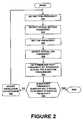
- FIG. 2shows a flow diagram of a method for centering an operation band about a desired operating frequency of a voltage controlled oscillator in accordance with one embodiment of the present invention.
- FIG. 3Ashows a block diagram of a phase lock loop voltage controlled oscillator in accordance with one embodiment of the present invention.
- FIG. 3Bshows a capacitor bank of a voltage controlled oscillator in accordance with an exemplary embodiment of the present invention.
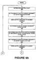
- FIGS. 4A-4Bshow a flow diagram of a method of centering an operating band about a desired operating frequency of a phase lock loop voltage controlled oscillator in accordance with one embodiment of the present invention.
- FIG. 5shows a block diagram of a control logic of a PLL VCO, in accordance with one embodiment of the present invention.
- FIG. 2a flow diagram of a method for centering an operating band about a desired operating frequency of a voltage controlled oscillator (VC 0 ) in accordance with one embodiment of the present invention is shown.
- the processbegins by setting a bottom frequency (e.g., a lower most operating frequency) at step 210 .
- the actual bottom frequency generatedis detected.
- the top frequencye.g., an upper most operating frequency within the operating band
- the actual top frequency generatedis detected.
- the actual bottom frequency and actual top frequencyare averaged together to determine a mid-point frequency of the operating band, at step 230 .
- the mid-point frequencyis then compared to a desired operating frequency, at step 235 .
- a capacitance of the VCOis adjusted according to the comparison between the mid-point frequency and the desired operating frequency. Adjusting the capacitance of the VCO results in the actual bottom and top frequencies being changed. Steps 210 - 240 , are iteratively performed until the mid-point frequency substantially equals the desired operating frequency.
- a capacitance bankcomprising a plurality of capacitors arranged in parallel, may be utilized to adjust the capacitance of the VCO.
- Each capacitormay be selectively switched in or out of the VCO circuit. The process may begin with approximately half the capacitance value switched into the VCO circuit.
- one or more capacitorsare the successively switched into or out of the VCO circuit until the operating band is centered about a desired operating frequency.
- the PLL VCO 300comprises a reference clock 310 , a phase/frequency detector 315 , a charge pump 320 , a voltage controlled oscillator (VCO) 325 , an adjustable feedback divider 330 , an adjustable period divider 335 , a counter 340 , and control logic 345 .
- VCOvoltage controlled oscillator
- the phase-frequency detector 315is responsive to a reference clock 350 and a feedback clock 355 .
- the phase-frequency detector 315may provide one or more out-of-lock indicative signals corresponding to whether and to what extent the feedback clock 355 is out-of-lock with the reference clock 350 .
- the out-of-lock indicative signalsmay be up and down signals 360 365 .
- the charge pump 320is responsive to the out-of-lock indicative signals, and provides for generating a control signal 370 whose voltage potential corresponds to a phase error between the feedback clock 355 and the reference clock 350 .
- the VCO 325is responsive to the control signal 370 , and provides for generating an output signal 375 .
- the output signal 375 of the VCO 325has a desired operating frequency (e.g., 2.44 GHz) within the operating band (e.g. 2.2 GHz to 3.2 GHz) of the VCO 325 .
- the control logic 345receives a first and a second input 390 , e.g., from a user, specifying a feedback divide value N and a period divide value P, respectively.
- the control logicselectively controls the divide values N and P of the adjustable feedback divider 330 and the adjustable period divider 335 respectively in response to said fist and second user inputs 390 .
- the adjustable feedback divider 330reduces the frequency of the output signal (e.g., 2.44 GHz) 375 , according to the feedback divide value N.
- the adjustable feedback dividerprovides a feedback clock 355 to the phase/frequency detector 315 and the adjustable period divider 335 .
- the adjustable period divider 335reduces the feedback clock 355 , according to the period divide value P.
- the adjustable period dividerprovides a period clock 380 .
- the counter 340counts the number of reference clock 350 cycles that occur during a cycle of the period clock 380 and outputs the results to the control logic 345 .
- the control logic 345provides the count value as an output to the user.
- the value of Nis selected such that the VCO 325 operates at its lowest possible operating point within the operating band (e.g. the PLL VCO 300 will not be successful in locking onto a frequency that will resolve the difference between feedback clock 355 and the reference clock 350 ).
- the feedback clock 355runs at a frequency greater than the reference clock 350 .
- the phase/frequency detector 315outputs an out-of-lock signal 360 , 365 such that the VCO 325 is driven to provide an output signal 375 having a slowest possible frequency.
- Pperiod divide value
- the value of Nis selected such that the VCO 325 operates at its highest possible operating point within the operating band (e.g. the PLL VCO 300 will not be successful in locking onto a frequency that will resolve the difference between feedback clock 355 and the reference clock 350 ).
- the feedback clock 355runs at a frequency less than the reference clock 350 .
- the phase/frequency detector 315outputs an out-of-lock signal 360 , 365 such that the VCO 325 is driven to provide an output signal 375 having a fastest possible frequency.
- the usercan average the low and high count values and compare it to an expected count value. If the measured average value is higher than the expected count value, the mid-point of the operating band of the VCO 325 is too high. Hence, there is too much capacitance to charge. If the measured average value is lower than the expected count value, the mid-point of the operating band of the VCO 325 is too low. Hence there is not enough capacitance to charge.
- the low and high count valuescan be summed, instead of averaged. In such an implementation, the expected count value is adjusted accordingly.
- the capacitor bankcomprises a plurality of parallel capacitors (C 1 , C 2 , C 3 , C 4 , C 5 , and C 6 , C 7 , C 8 , C 9 , C 10 ) that can be selectively switched in and out by a plurality of switching elements (MP 1 , MP 2 , MP 3 , MP 4 , MP 5 , and MP 6 , MP 7 , MP 8 , MP 9 , MP 10 ).
- a plurality of parallel capacitorsC 1 , C 2 , C 3 , C 4 , C 5 , and C 6 , C 7 , C 8 , C 9 , C 10
- the capacitor bankis coupled between a pair of nodes (e.g., Vreg), which effect the operating band of the voltage controlled oscillator.
- Vregnodes
- the exemplary capacitor bankis illustrative of a differential VCO implementation.
- a single-ended VCO implementationonly requires a left or right half of the exemplary capacitor bank.
- Control signals(e.g., I 1 , I 2 , I 3 , I 4 , I 5 ) 385 received from the control logic 345 are utilized to control the switching state of the switching elements (MP 1 , MP 2 , MP 3 , MP 4 , MP 5 , and MP 6 , MP 7 , MP 8 , MP 9 , MP 10 ).
- switching elementse.g., MP 5 , MP 6
- the corresponding capacitorse.g., C 5 , C 6
- switching elementse.g., MP 5 , MP 6
- a corresponding control signale.g., I 5
- the corresponding capacitorse.g., C 5 , C 6
- the available capacitanceis divided into a combination of discrete capacitors.
- the capacitance valuesare all equal.
- the initial condition of the capacitance bank 326may be such that the most significant capacitances (e.g., C 5 , C 6 ) are switched in and the less significant capacitances (e.g., C 1 , C 2 , C 3 , C 4 , C 7 , C 8 , C 9 , C 10 ) are switched out.
- the current significant capacitances(e.g., C 5 , C 10 ) are switched out, and the next most significant capacitors are switched in (e.g., C 4 , C 7 ) by the switching signals (e.g., I 1 , I 2 , I 3 , I 4 ) 385 from the control logic 345 .
- the current significant capacitances(e.g., C 5 , C 10 ) are left switched in, and the next most significant capacitors (e.g., C 4 , C 7 ) are also switched in by the switching signals (e.g., I 1 , I 2 , I 3 , I 4 ) 385 from the control logic 345 .
- the process of calculating the low and high operating points of the operating bandis repeated, for each discrete capacitor in the capacitor bank 326 .
- a maximum number of passesequal to the number of capacitors in the capacitance bank 326 (e.g., five) are required to center the operating band about a desired operating frequency.
- the capacitance bankmay also be utilized to compensate for process variations and operating temperature variations. Process variation occurring during fabrication of the VCO circuit result in shifting of the operating band from one VCO circuit to another.
- the capacitance bankwhich provides for selectively adjusting the capacitance of each VCO circuit, can be utilized to compensate for process variations in the VCO circuit.
- variations in the operating temperature between one VCO circuit and anotherresult in a shift of the operating band of one VCO circuit with respect to another.
- the capacitance bankcan also be utilized to compensate for operating temperature variations.
- the state of the capacitance bank 326may be permanently set by any well-known method, such as selectively opening one or more fusible links.
- FIGS. 4A-4Ba flow diagram of a method of centering an operating band (e.g., 2.2 GHz to 3.2 GHz) about a desired operating frequency (e.g., 2.44 GHz) of a phase lock loop voltage controlled oscillator (PLL VCO) in accordance with one embodiment of the present invention is shown.
- the processbegins by determining an expected count value, at step 405 .
- a desired center frequencye.g.,2.44 GHz
- Ne.g., 3200 or 1600
- the expected count valuee.g., 64.8 is then obtained by dividing the frequency of a reference clock (e.g., 1 MHz) by the expected period clock.
- the frequency of the output signal of the voltage controlled oscillatoris driven to the highest possible point in the operating band (e.g., 3.2 GHz).
- a high count valueis determined by counting the number of reference clock cycles during a cycle of the period clock (e.g., 50 counts).
- the frequency of the output signal of the voltage controlled oscillatoris driven to the lowest possible point in the operating band (e.g., 2.2 GHz).
- a low count valueis determined by counting the number of reference clock cycles during a cycle of the period clock (e.g., 74.8 counts).
- an actual countis determined by averaging the high count and low count values.
- the actual counte.g., 62.4
- the expected count64.8
- a next most significant capacitor, in a binary weighted capacitor bank, of the VCOis switched in, at step 460 . If the average count is not less than the expected count, a current significant capacitor is switched out and the next most significant capacitor is switched in, at step 465 .
- the above-described processis repeated for each capacitor in the binary weighted capacitance bank, starting with the most significant capacitor and ending with the least significant capacitor.
- control logic 505of a PLL VCO, in accordance with one embodiment of the present invention is shown.
- the control logic 505comprises a register 510 , an added 515 , a shift register 520 , an ideal count register 525 , a comparator 530 , and a switch circuit 535 .
- a counter 540is coupled to the register 510 and the adder 515 .
- the register 510is also coupled to the adder 515 .
- the adder 515is coupled to the shift register 520 .
- the shift register 520 and the ideal count register 525are coupled to the comparator 530 .
- the comparatoris coupled to the switch circuit 535 .
- the counterreceives a start signal and an increment signal.
- the start signalcomprises a period clock 540 .
- the increment signalcomprises a reference clock 545 .
- the counter 540increments in response to each occurrence of the increment signal 545 .
- the value contained in the counter 540is shifted into the register 510 .
- the counter 540is also reset, and upon the occurrence of a third start signal 540 , the counter is incremented again.
- the shift register 520contains the average of the values contained in the counter 540 and the register 510 .
- the comparator 530then compared average to an ideal count contained in the ideal counter 525 . Based upon whether the average count or ideal count value is larger, more or less capacitance, in a capacitor bank 550 , is selectively added by the switch circuit 535 .
- the control logic 505iteratively determines successive average count values and adjusts the capacitor bank 505 accordingly.
- control logicperforms the successive approximation routine of the present embodiment in response to a control signal received on an external pin. In another implementation, the control logic performs the successive approximation routine of the present embodiment in response to an internally generated control signal. In another embodiment, the control logic also performs initialization of the various registers, counters, dividers, switches, and the like.
- Embodiments of the present inventionare advantageous in that a minimal operating band of the PLL VCO is required. Embodiments of the present invention are advantageous in that the PLL VCO is less susceptible to noise and interference. Embodiments of the present invention are advantageous in that changes in temperature can be readily compensated for. Embodiments of the present invention are advantageous in that component and process variations can be readily compensated for.
Landscapes
- Stabilization Of Oscillater, Synchronisation, Frequency Synthesizers (AREA)
Abstract
Description
Claims (20)
Priority Applications (1)
| Application Number | Priority Date | Filing Date | Title |
|---|---|---|---|
| US10/327,354US6903613B1 (en) | 2002-12-20 | 2002-12-20 | Voltage controlled oscillator |
Applications Claiming Priority (1)
| Application Number | Priority Date | Filing Date | Title |
|---|---|---|---|
| US10/327,354US6903613B1 (en) | 2002-12-20 | 2002-12-20 | Voltage controlled oscillator |
Publications (1)
| Publication Number | Publication Date |
|---|---|
| US6903613B1true US6903613B1 (en) | 2005-06-07 |
Family
ID=34619200
Family Applications (1)
| Application Number | Title | Priority Date | Filing Date |
|---|---|---|---|
| US10/327,354Expired - LifetimeUS6903613B1 (en) | 2002-12-20 | 2002-12-20 | Voltage controlled oscillator |
Country Status (1)
| Country | Link |
|---|---|
| US (1) | US6903613B1 (en) |
Cited By (51)
| Publication number | Priority date | Publication date | Assignee | Title |
|---|---|---|---|---|
| US20060049887A1 (en)* | 2003-02-27 | 2006-03-09 | Christian Munker | Phase regulating arrangement |
| US7023285B2 (en)* | 2003-07-15 | 2006-04-04 | Telefonaktiebolaget Lm Ericsson (Publ) | Self-calibrating controllable oscillator |
| US20060152290A1 (en)* | 2004-09-22 | 2006-07-13 | Kyeongho Lee | Apparatus and method of oscillating wideband frequency |
| WO2006036749A3 (en)* | 2004-09-22 | 2006-09-28 | Gct Semiconductor Inc | Apparatus and method of oscillating wideband frequency |
| US20060258313A1 (en)* | 2002-05-31 | 2006-11-16 | Toshiya Uozumi | Circuit having a multi-band oscillator and compensating oscillation frequency |
| US20070001770A1 (en)* | 2005-06-20 | 2007-01-04 | Airoha Technology Corp. | Phase lock loop and operating method thereof |
| US20070121774A1 (en)* | 2005-11-25 | 2007-05-31 | Samsung Electronics Co., Ltd. | Phase-locked loop for stably adjusting frequency-band of voltage-controlled oscillator and phase locking method |
| US7265633B1 (en) | 2004-06-14 | 2007-09-04 | Cypress Semiconductor Corporation | Open loop bandwidth test architecture and method for phase locked loop (PLL) |
| US20090153252A1 (en)* | 2007-12-13 | 2009-06-18 | Mei-Show Chen | Multi-band voltage controlled oscillator controlling module, phase locked loop utilizing which and related method thereof |
| US7737724B2 (en) | 2007-04-17 | 2010-06-15 | Cypress Semiconductor Corporation | Universal digital block interconnection and channel routing |
| US7761845B1 (en) | 2002-09-09 | 2010-07-20 | Cypress Semiconductor Corporation | Method for parameterizing a user module |
| US7765095B1 (en) | 2000-10-26 | 2010-07-27 | Cypress Semiconductor Corporation | Conditional branching in an in-circuit emulation system |
| US7770113B1 (en) | 2001-11-19 | 2010-08-03 | Cypress Semiconductor Corporation | System and method for dynamically generating a configuration datasheet |
| US7774190B1 (en) | 2001-11-19 | 2010-08-10 | Cypress Semiconductor Corporation | Sleep and stall in an in-circuit emulation system |
| US7825688B1 (en) | 2000-10-26 | 2010-11-02 | Cypress Semiconductor Corporation | Programmable microcontroller architecture(mixed analog/digital) |
| US7844437B1 (en) | 2001-11-19 | 2010-11-30 | Cypress Semiconductor Corporation | System and method for performing next placements and pruning of disallowed placements for programming an integrated circuit |
| US7893724B2 (en) | 2004-03-25 | 2011-02-22 | Cypress Semiconductor Corporation | Method and circuit for rapid alignment of signals |
| US8026739B2 (en) | 2007-04-17 | 2011-09-27 | Cypress Semiconductor Corporation | System level interconnect with programmable switching |
| US8040266B2 (en) | 2007-04-17 | 2011-10-18 | Cypress Semiconductor Corporation | Programmable sigma-delta analog-to-digital converter |
| US8049569B1 (en) | 2007-09-05 | 2011-11-01 | Cypress Semiconductor Corporation | Circuit and method for improving the accuracy of a crystal-less oscillator having dual-frequency modes |
| US8069436B2 (en) | 2004-08-13 | 2011-11-29 | Cypress Semiconductor Corporation | Providing hardware independence to automate code generation of processing device firmware |
| US8069405B1 (en) | 2001-11-19 | 2011-11-29 | Cypress Semiconductor Corporation | User interface for efficiently browsing an electronic document using data-driven tabs |
| US8069428B1 (en) | 2001-10-24 | 2011-11-29 | Cypress Semiconductor Corporation | Techniques for generating microcontroller configuration information |
| US8067948B2 (en) | 2006-03-27 | 2011-11-29 | Cypress Semiconductor Corporation | Input/output multiplexer bus |
| US8078894B1 (en) | 2007-04-25 | 2011-12-13 | Cypress Semiconductor Corporation | Power management architecture, method and configuration system |
| US8078970B1 (en) | 2001-11-09 | 2011-12-13 | Cypress Semiconductor Corporation | Graphical user interface with user-selectable list-box |
| US8085067B1 (en) | 2005-12-21 | 2011-12-27 | Cypress Semiconductor Corporation | Differential-to-single ended signal converter circuit and method |
| US8085100B2 (en) | 2005-02-04 | 2011-12-27 | Cypress Semiconductor Corporation | Poly-phase frequency synthesis oscillator |
| US8089461B2 (en) | 2005-06-23 | 2012-01-03 | Cypress Semiconductor Corporation | Touch wake for electronic devices |
| US8092083B2 (en) | 2007-04-17 | 2012-01-10 | Cypress Semiconductor Corporation | Temperature sensor with digital bandgap |
| US8103496B1 (en) | 2000-10-26 | 2012-01-24 | Cypress Semicondutor Corporation | Breakpoint control in an in-circuit emulation system |
| US8103497B1 (en) | 2002-03-28 | 2012-01-24 | Cypress Semiconductor Corporation | External interface for event architecture |
| US8120408B1 (en) | 2005-05-05 | 2012-02-21 | Cypress Semiconductor Corporation | Voltage controlled oscillator delay cell and method |
| US8130025B2 (en) | 2007-04-17 | 2012-03-06 | Cypress Semiconductor Corporation | Numerical band gap |
| US8149048B1 (en) | 2000-10-26 | 2012-04-03 | Cypress Semiconductor Corporation | Apparatus and method for programmable power management in a programmable analog circuit block |
| US8160864B1 (en) | 2000-10-26 | 2012-04-17 | Cypress Semiconductor Corporation | In-circuit emulator and pod synchronized boot |
| US8176296B2 (en) | 2000-10-26 | 2012-05-08 | Cypress Semiconductor Corporation | Programmable microcontroller architecture |
| US8286125B2 (en) | 2004-08-13 | 2012-10-09 | Cypress Semiconductor Corporation | Model for a hardware device-independent method of defining embedded firmware for programmable systems |
| US8402313B1 (en) | 2002-05-01 | 2013-03-19 | Cypress Semiconductor Corporation | Reconfigurable testing system and method |
| US8499270B1 (en) | 2007-04-25 | 2013-07-30 | Cypress Semiconductor Corporation | Configuration of programmable IC design elements |
| US8516025B2 (en) | 2007-04-17 | 2013-08-20 | Cypress Semiconductor Corporation | Clock driven dynamic datapath chaining |
| US8533677B1 (en) | 2001-11-19 | 2013-09-10 | Cypress Semiconductor Corporation | Graphical user interface for dynamically reconfiguring a programmable device |
| US8618840B1 (en)* | 2012-07-11 | 2013-12-31 | Fujitsu Limited | Frequency synthesizer tuning |
| US20160197601A1 (en)* | 2015-01-01 | 2016-07-07 | Sang-Wook Han | Frequency synthesizer and method controlling frequency synthesizer |
| US9448964B2 (en) | 2009-05-04 | 2016-09-20 | Cypress Semiconductor Corporation | Autonomous control in a programmable system |
| US9564902B2 (en) | 2007-04-17 | 2017-02-07 | Cypress Semiconductor Corporation | Dynamically configurable and re-configurable data path |
| US9720805B1 (en) | 2007-04-25 | 2017-08-01 | Cypress Semiconductor Corporation | System and method for controlling a target device |
| US20170346496A1 (en)* | 2014-12-16 | 2017-11-30 | Nordic Semiconductor Asa | Oscillator calibration |
| CN111181552A (en)* | 2020-01-08 | 2020-05-19 | 电子科技大学 | A bidirectional frequency synchronous oscillator circuit |
| US10698662B2 (en) | 2001-11-15 | 2020-06-30 | Cypress Semiconductor Corporation | System providing automatic source code generation for personalization and parameterization of user modules |
| CN115133925A (en)* | 2021-03-26 | 2022-09-30 | 中国科学院国家天文台 | Quick calibration method and circuit for voltage-controlled oscillator |
Citations (20)
| Publication number | Priority date | Publication date | Assignee | Title |
|---|---|---|---|---|
| US5581216A (en) | 1995-01-24 | 1996-12-03 | Ic Works, Inc. | Low jitter voltage controlled oscillator (VCO) circuit |
| US5640523A (en) | 1994-09-02 | 1997-06-17 | Cypress Semiconductor Corporation | Method and apparatus for a pulsed tri-state phase detector for reduced jitter clock recovery |
| US5648744A (en) | 1995-12-22 | 1997-07-15 | Microtune, Inc. | System and method for voltage controlled oscillator automatic band selection |
| US5745011A (en) | 1996-06-05 | 1998-04-28 | Cypress Semiconductor Corporation | Data recovery phase locked loop |
| US5748048A (en) | 1996-12-12 | 1998-05-05 | Cypress Semiconductor Corporation | Voltage controlled oscillator (VCO) frequency gain compensation circuit |
| US5926041A (en) | 1997-06-19 | 1999-07-20 | Cypress Semiconductorcorp. | Phase detector with linear output response |
| US6026134A (en) | 1997-06-19 | 2000-02-15 | Cypress Semiconductor Corp. | Phase locked loop (PLL) with linear parallel sampling phase detector |
| US6337604B1 (en) | 1999-05-14 | 2002-01-08 | Telefonaktiebolaget Lm Ericsson (Publ) | Crystal oscillator |
| US6404294B1 (en) | 2000-07-18 | 2002-06-11 | Cypress Semiconductor Corp. | Voltage control oscillator (VCO) with automatic gain control |
| US6434187B1 (en) | 1997-10-14 | 2002-08-13 | Cypress Semiconductor Corp. | Digital radiofrequency transceiver |
| US6658748B1 (en) | 2000-03-02 | 2003-12-09 | Texas Instruments Incorporated | Digitally-controlled L-C oscillator |
| US6686804B1 (en) | 2001-03-19 | 2004-02-03 | Cisco Systems Wireless Networking (Australia) Pty. Limited | Frequency synthesizer using a VCO having a controllable operating point, and calibration and tuning thereof |
| US6710669B2 (en) | 2001-05-18 | 2004-03-23 | Nippon Precision Circuits Inc. | Voltage controlled oscillator |
| US6731209B2 (en) | 2001-02-07 | 2004-05-04 | Gerenraich Family Trust | Control system with capacitive detector |
| US6744323B1 (en) | 2001-08-30 | 2004-06-01 | Cypress Semiconductor Corp. | Method for phase locking in a phase lock loop |
| US6744324B1 (en)* | 2001-03-19 | 2004-06-01 | Cisco Technology, Inc. | Frequency synthesizer using a VCO having a controllable operating point, and calibration and tuning thereof |
| US6747522B2 (en) | 2002-05-03 | 2004-06-08 | Silicon Laboratories, Inc. | Digitally controlled crystal oscillator with integrated coarse and fine control |
| US6791421B2 (en) | 2001-10-24 | 2004-09-14 | Nihon Dempa Kogyo Co., Ltd. | Input-switching voltage-controlled oscillator and PLL-controlled oscillator |
| US6798296B2 (en) | 2002-03-28 | 2004-09-28 | Texas Instruments Incorporated | Wide band, wide operation range, general purpose digital phase locked loop architecture |
| US6803830B2 (en) | 2001-07-17 | 2004-10-12 | Texas Instruments Incorporated | Phase-locked loop and method for automatically setting its output frequency |
- 2002
- 2002-12-20USUS10/327,354patent/US6903613B1/ennot_activeExpired - Lifetime
Patent Citations (21)
| Publication number | Priority date | Publication date | Assignee | Title |
|---|---|---|---|---|
| US5640523A (en) | 1994-09-02 | 1997-06-17 | Cypress Semiconductor Corporation | Method and apparatus for a pulsed tri-state phase detector for reduced jitter clock recovery |
| US5581216A (en) | 1995-01-24 | 1996-12-03 | Ic Works, Inc. | Low jitter voltage controlled oscillator (VCO) circuit |
| US5648744A (en) | 1995-12-22 | 1997-07-15 | Microtune, Inc. | System and method for voltage controlled oscillator automatic band selection |
| US5745011A (en) | 1996-06-05 | 1998-04-28 | Cypress Semiconductor Corporation | Data recovery phase locked loop |
| US5748048A (en) | 1996-12-12 | 1998-05-05 | Cypress Semiconductor Corporation | Voltage controlled oscillator (VCO) frequency gain compensation circuit |
| US5896068A (en) | 1996-12-12 | 1999-04-20 | Cypress Semiconductor Corp. | Voltage controlled oscillator (VCO) frequency gain compensation circuit |
| US5926041A (en) | 1997-06-19 | 1999-07-20 | Cypress Semiconductorcorp. | Phase detector with linear output response |
| US6026134A (en) | 1997-06-19 | 2000-02-15 | Cypress Semiconductor Corp. | Phase locked loop (PLL) with linear parallel sampling phase detector |
| US6434187B1 (en) | 1997-10-14 | 2002-08-13 | Cypress Semiconductor Corp. | Digital radiofrequency transceiver |
| US6337604B1 (en) | 1999-05-14 | 2002-01-08 | Telefonaktiebolaget Lm Ericsson (Publ) | Crystal oscillator |
| US6658748B1 (en) | 2000-03-02 | 2003-12-09 | Texas Instruments Incorporated | Digitally-controlled L-C oscillator |
| US6404294B1 (en) | 2000-07-18 | 2002-06-11 | Cypress Semiconductor Corp. | Voltage control oscillator (VCO) with automatic gain control |
| US6731209B2 (en) | 2001-02-07 | 2004-05-04 | Gerenraich Family Trust | Control system with capacitive detector |
| US6686804B1 (en) | 2001-03-19 | 2004-02-03 | Cisco Systems Wireless Networking (Australia) Pty. Limited | Frequency synthesizer using a VCO having a controllable operating point, and calibration and tuning thereof |
| US6744324B1 (en)* | 2001-03-19 | 2004-06-01 | Cisco Technology, Inc. | Frequency synthesizer using a VCO having a controllable operating point, and calibration and tuning thereof |
| US6710669B2 (en) | 2001-05-18 | 2004-03-23 | Nippon Precision Circuits Inc. | Voltage controlled oscillator |
| US6803830B2 (en) | 2001-07-17 | 2004-10-12 | Texas Instruments Incorporated | Phase-locked loop and method for automatically setting its output frequency |
| US6744323B1 (en) | 2001-08-30 | 2004-06-01 | Cypress Semiconductor Corp. | Method for phase locking in a phase lock loop |
| US6791421B2 (en) | 2001-10-24 | 2004-09-14 | Nihon Dempa Kogyo Co., Ltd. | Input-switching voltage-controlled oscillator and PLL-controlled oscillator |
| US6798296B2 (en) | 2002-03-28 | 2004-09-28 | Texas Instruments Incorporated | Wide band, wide operation range, general purpose digital phase locked loop architecture |
| US6747522B2 (en) | 2002-05-03 | 2004-06-08 | Silicon Laboratories, Inc. | Digitally controlled crystal oscillator with integrated coarse and fine control |
Cited By (73)
| Publication number | Priority date | Publication date | Assignee | Title |
|---|---|---|---|---|
| US8736303B2 (en) | 2000-10-26 | 2014-05-27 | Cypress Semiconductor Corporation | PSOC architecture |
| US10725954B2 (en) | 2000-10-26 | 2020-07-28 | Monterey Research, Llc | Microcontroller programmable system on a chip |
| US7825688B1 (en) | 2000-10-26 | 2010-11-02 | Cypress Semiconductor Corporation | Programmable microcontroller architecture(mixed analog/digital) |
| US8103496B1 (en) | 2000-10-26 | 2012-01-24 | Cypress Semicondutor Corporation | Breakpoint control in an in-circuit emulation system |
| US10261932B2 (en) | 2000-10-26 | 2019-04-16 | Cypress Semiconductor Corporation | Microcontroller programmable system on a chip |
| US10248604B2 (en) | 2000-10-26 | 2019-04-02 | Cypress Semiconductor Corporation | Microcontroller programmable system on a chip |
| US10020810B2 (en) | 2000-10-26 | 2018-07-10 | Cypress Semiconductor Corporation | PSoC architecture |
| US9843327B1 (en) | 2000-10-26 | 2017-12-12 | Cypress Semiconductor Corporation | PSOC architecture |
| US7765095B1 (en) | 2000-10-26 | 2010-07-27 | Cypress Semiconductor Corporation | Conditional branching in an in-circuit emulation system |
| US9766650B2 (en) | 2000-10-26 | 2017-09-19 | Cypress Semiconductor Corporation | Microcontroller programmable system on a chip with programmable interconnect |
| US8358150B1 (en) | 2000-10-26 | 2013-01-22 | Cypress Semiconductor Corporation | Programmable microcontroller architecture(mixed analog/digital) |
| US8555032B2 (en) | 2000-10-26 | 2013-10-08 | Cypress Semiconductor Corporation | Microcontroller programmable system on a chip with programmable interconnect |
| US8149048B1 (en) | 2000-10-26 | 2012-04-03 | Cypress Semiconductor Corporation | Apparatus and method for programmable power management in a programmable analog circuit block |
| US8176296B2 (en) | 2000-10-26 | 2012-05-08 | Cypress Semiconductor Corporation | Programmable microcontroller architecture |
| US8160864B1 (en) | 2000-10-26 | 2012-04-17 | Cypress Semiconductor Corporation | In-circuit emulator and pod synchronized boot |
| US8069428B1 (en) | 2001-10-24 | 2011-11-29 | Cypress Semiconductor Corporation | Techniques for generating microcontroller configuration information |
| US8793635B1 (en) | 2001-10-24 | 2014-07-29 | Cypress Semiconductor Corporation | Techniques for generating microcontroller configuration information |
| US10466980B2 (en) | 2001-10-24 | 2019-11-05 | Cypress Semiconductor Corporation | Techniques for generating microcontroller configuration information |
| US8078970B1 (en) | 2001-11-09 | 2011-12-13 | Cypress Semiconductor Corporation | Graphical user interface with user-selectable list-box |
| US10698662B2 (en) | 2001-11-15 | 2020-06-30 | Cypress Semiconductor Corporation | System providing automatic source code generation for personalization and parameterization of user modules |
| US7770113B1 (en) | 2001-11-19 | 2010-08-03 | Cypress Semiconductor Corporation | System and method for dynamically generating a configuration datasheet |
| US7774190B1 (en) | 2001-11-19 | 2010-08-10 | Cypress Semiconductor Corporation | Sleep and stall in an in-circuit emulation system |
| US8370791B2 (en) | 2001-11-19 | 2013-02-05 | Cypress Semiconductor Corporation | System and method for performing next placements and pruning of disallowed placements for programming an integrated circuit |
| US8533677B1 (en) | 2001-11-19 | 2013-09-10 | Cypress Semiconductor Corporation | Graphical user interface for dynamically reconfiguring a programmable device |
| US7844437B1 (en) | 2001-11-19 | 2010-11-30 | Cypress Semiconductor Corporation | System and method for performing next placements and pruning of disallowed placements for programming an integrated circuit |
| US8069405B1 (en) | 2001-11-19 | 2011-11-29 | Cypress Semiconductor Corporation | User interface for efficiently browsing an electronic document using data-driven tabs |
| US8103497B1 (en) | 2002-03-28 | 2012-01-24 | Cypress Semiconductor Corporation | External interface for event architecture |
| US8402313B1 (en) | 2002-05-01 | 2013-03-19 | Cypress Semiconductor Corporation | Reconfigurable testing system and method |
| US7263340B2 (en)* | 2002-05-31 | 2007-08-28 | Renesas Technology Corporation | PLL circuit having a multi-band oscillator and compensating oscillation frequency |
| US20060258313A1 (en)* | 2002-05-31 | 2006-11-16 | Toshiya Uozumi | Circuit having a multi-band oscillator and compensating oscillation frequency |
| US7761845B1 (en) | 2002-09-09 | 2010-07-20 | Cypress Semiconductor Corporation | Method for parameterizing a user module |
| US7154342B2 (en)* | 2003-02-27 | 2006-12-26 | Infineon Technologies Ag | Phase locked loop circuit with a tunable oscillator and an independent frequency converter and frequency counter |
| US20060049887A1 (en)* | 2003-02-27 | 2006-03-09 | Christian Munker | Phase regulating arrangement |
| US7023285B2 (en)* | 2003-07-15 | 2006-04-04 | Telefonaktiebolaget Lm Ericsson (Publ) | Self-calibrating controllable oscillator |
| US7893724B2 (en) | 2004-03-25 | 2011-02-22 | Cypress Semiconductor Corporation | Method and circuit for rapid alignment of signals |
| US7265633B1 (en) | 2004-06-14 | 2007-09-04 | Cypress Semiconductor Corporation | Open loop bandwidth test architecture and method for phase locked loop (PLL) |
| US8286125B2 (en) | 2004-08-13 | 2012-10-09 | Cypress Semiconductor Corporation | Model for a hardware device-independent method of defining embedded firmware for programmable systems |
| US8069436B2 (en) | 2004-08-13 | 2011-11-29 | Cypress Semiconductor Corporation | Providing hardware independence to automate code generation of processing device firmware |
| US20060152290A1 (en)* | 2004-09-22 | 2006-07-13 | Kyeongho Lee | Apparatus and method of oscillating wideband frequency |
| WO2006036749A3 (en)* | 2004-09-22 | 2006-09-28 | Gct Semiconductor Inc | Apparatus and method of oscillating wideband frequency |
| US7190236B2 (en)* | 2004-09-22 | 2007-03-13 | Gct Semiconductor Inc. | Apparatus and method of oscillating wideband frequency |
| US8085100B2 (en) | 2005-02-04 | 2011-12-27 | Cypress Semiconductor Corporation | Poly-phase frequency synthesis oscillator |
| US8120408B1 (en) | 2005-05-05 | 2012-02-21 | Cypress Semiconductor Corporation | Voltage controlled oscillator delay cell and method |
| US7511579B2 (en)* | 2005-06-20 | 2009-03-31 | Airoha Technology Corp. | Phase lock loop and operating method thereof |
| US20070001770A1 (en)* | 2005-06-20 | 2007-01-04 | Airoha Technology Corp. | Phase lock loop and operating method thereof |
| US8089461B2 (en) | 2005-06-23 | 2012-01-03 | Cypress Semiconductor Corporation | Touch wake for electronic devices |
| US20070121774A1 (en)* | 2005-11-25 | 2007-05-31 | Samsung Electronics Co., Ltd. | Phase-locked loop for stably adjusting frequency-band of voltage-controlled oscillator and phase locking method |
| US7471159B2 (en)* | 2005-11-25 | 2008-12-30 | Samsung Electronics Co., Ltd. | Phase-locked loop for stably adjusting frequency-band of voltage-controlled oscillator and phase locking method |
| US8085067B1 (en) | 2005-12-21 | 2011-12-27 | Cypress Semiconductor Corporation | Differential-to-single ended signal converter circuit and method |
| US8717042B1 (en) | 2006-03-27 | 2014-05-06 | Cypress Semiconductor Corporation | Input/output multiplexer bus |
| US8067948B2 (en) | 2006-03-27 | 2011-11-29 | Cypress Semiconductor Corporation | Input/output multiplexer bus |
| US8516025B2 (en) | 2007-04-17 | 2013-08-20 | Cypress Semiconductor Corporation | Clock driven dynamic datapath chaining |
| US7737724B2 (en) | 2007-04-17 | 2010-06-15 | Cypress Semiconductor Corporation | Universal digital block interconnection and channel routing |
| US8130025B2 (en) | 2007-04-17 | 2012-03-06 | Cypress Semiconductor Corporation | Numerical band gap |
| US8476928B1 (en) | 2007-04-17 | 2013-07-02 | Cypress Semiconductor Corporation | System level interconnect with programmable switching |
| US8092083B2 (en) | 2007-04-17 | 2012-01-10 | Cypress Semiconductor Corporation | Temperature sensor with digital bandgap |
| US8026739B2 (en) | 2007-04-17 | 2011-09-27 | Cypress Semiconductor Corporation | System level interconnect with programmable switching |
| US8040266B2 (en) | 2007-04-17 | 2011-10-18 | Cypress Semiconductor Corporation | Programmable sigma-delta analog-to-digital converter |
| US9564902B2 (en) | 2007-04-17 | 2017-02-07 | Cypress Semiconductor Corporation | Dynamically configurable and re-configurable data path |
| US8909960B1 (en) | 2007-04-25 | 2014-12-09 | Cypress Semiconductor Corporation | Power management architecture, method and configuration system |
| US8078894B1 (en) | 2007-04-25 | 2011-12-13 | Cypress Semiconductor Corporation | Power management architecture, method and configuration system |
| US9720805B1 (en) | 2007-04-25 | 2017-08-01 | Cypress Semiconductor Corporation | System and method for controlling a target device |
| US8499270B1 (en) | 2007-04-25 | 2013-07-30 | Cypress Semiconductor Corporation | Configuration of programmable IC design elements |
| US8049569B1 (en) | 2007-09-05 | 2011-11-01 | Cypress Semiconductor Corporation | Circuit and method for improving the accuracy of a crystal-less oscillator having dual-frequency modes |
| US20090153252A1 (en)* | 2007-12-13 | 2009-06-18 | Mei-Show Chen | Multi-band voltage controlled oscillator controlling module, phase locked loop utilizing which and related method thereof |
| US9448964B2 (en) | 2009-05-04 | 2016-09-20 | Cypress Semiconductor Corporation | Autonomous control in a programmable system |
| US8618840B1 (en)* | 2012-07-11 | 2013-12-31 | Fujitsu Limited | Frequency synthesizer tuning |
| US10230382B2 (en)* | 2014-12-16 | 2019-03-12 | Nordic Semiconductor Asa | Oscillator calibration |
| US20170346496A1 (en)* | 2014-12-16 | 2017-11-30 | Nordic Semiconductor Asa | Oscillator calibration |
| US20160197601A1 (en)* | 2015-01-01 | 2016-07-07 | Sang-Wook Han | Frequency synthesizer and method controlling frequency synthesizer |
| US9762220B2 (en)* | 2015-01-02 | 2017-09-12 | Samsung Electronics Co., Ltd. | Frequency synthesizer and method controlling frequency synthesizer |
| CN111181552A (en)* | 2020-01-08 | 2020-05-19 | 电子科技大学 | A bidirectional frequency synchronous oscillator circuit |
| CN115133925A (en)* | 2021-03-26 | 2022-09-30 | 中国科学院国家天文台 | Quick calibration method and circuit for voltage-controlled oscillator |
Similar Documents
| Publication | Publication Date | Title |
|---|---|---|
| US6903613B1 (en) | Voltage controlled oscillator | |
| US9490827B2 (en) | Apparatus and methods for tuning a voltage controlled oscillator | |
| KR100847687B1 (en) | Frequency Synthesizer and Frequency Control Method | |
| US7129793B2 (en) | Device for calibrating the frequency of an oscillator, phase looked loop circuit comprising said calibration device and related frequency calibration method | |
| US7746182B2 (en) | Systems and methods for voltage controlled oscillator calibration | |
| US7786810B2 (en) | Phase locked loop with leakage current calibration | |
| US8487707B2 (en) | Frequency synthesizer | |
| US7443254B2 (en) | Relaxation oscillator with propagation delay compensation for improving the linearity and maximum frequency | |
| US7511579B2 (en) | Phase lock loop and operating method thereof | |
| US8519757B2 (en) | Apparatus and method for frequency calibration in frequency synthesizer | |
| US7772930B2 (en) | Calibration techniques for phase-locked loop bandwidth | |
| US7046093B1 (en) | Dynamic phase-locked loop circuits and methods of operation thereof | |
| US6774732B1 (en) | System and method for coarse tuning a phase locked loop (PLL) synthesizer using 2-PI slip detection | |
| US7436264B2 (en) | Charge supply apparatus and method in frequency synthesizer | |
| KR20060045054A (en) | Phase Control Loop Frequency Synthesizer | |
| US20080036544A1 (en) | Method for adjusting oscillator in phase-locked loop and related frequency synthesizer | |
| US7411467B2 (en) | Overtone crystal oscillator automatic calibration system | |
| JP2000049597A (en) | Pll circuit | |
| US7659785B2 (en) | Voltage controlled oscillator and PLL having the same | |
| US7432749B1 (en) | Circuit and method for improving frequency range in a phase locked loop | |
| KR100235370B1 (en) | Phase synchronizing circuit with feedback to control charge pump | |
| KR20190018936A (en) | Oscillator including varactor circuit and method of operation thereof | |
| KR100742016B1 (en) | Tunable Oscillator and Propagation Delay Compensation Method |
Legal Events
| Date | Code | Title | Description |
|---|---|---|---|
| AS | Assignment | Owner name:CYPRESS SEMICONDCUTOR CORPORATION, CALIFORNIA Free format text:ASSIGNMENT OF ASSIGNORS INTEREST;ASSIGNORS:MITCHELL, ERIC P.;GEHRING, MARK R.;REEL/FRAME:013972/0019 Effective date:20030217 | |
| STCF | Information on status: patent grant | Free format text:PATENTED CASE | |
| FEPP | Fee payment procedure | Free format text:PAYOR NUMBER ASSIGNED (ORIGINAL EVENT CODE: ASPN); ENTITY STATUS OF PATENT OWNER: LARGE ENTITY Free format text:PAYER NUMBER DE-ASSIGNED (ORIGINAL EVENT CODE: RMPN); ENTITY STATUS OF PATENT OWNER: LARGE ENTITY | |
| REMI | Maintenance fee reminder mailed | ||
| FPAY | Fee payment | Year of fee payment:4 | |
| SULP | Surcharge for late payment | ||
| FEPP | Fee payment procedure | Free format text:PAYOR NUMBER ASSIGNED (ORIGINAL EVENT CODE: ASPN); ENTITY STATUS OF PATENT OWNER: LARGE ENTITY Free format text:PAYER NUMBER DE-ASSIGNED (ORIGINAL EVENT CODE: RMPN); ENTITY STATUS OF PATENT OWNER: LARGE ENTITY | |
| FPAY | Fee payment | Year of fee payment:8 | |
| AS | Assignment | Owner name:TORREFY CONSULTING LLC, DELAWARE Free format text:ASSIGNMENT OF ASSIGNORS INTEREST;ASSIGNOR:CYPRESS SEMICONDUCTOR CORPORATION;REEL/FRAME:029089/0427 Effective date:20120907 | |
| AS | Assignment | Owner name:TAMIRAS PER PTE. LTD., LLC, DELAWARE Free format text:MERGER;ASSIGNOR:TORREFY CONSULTING LLC;REEL/FRAME:037297/0786 Effective date:20150903 | |
| FPAY | Fee payment | Year of fee payment:12 |