US6903001B2 - Techniques to create low K ILD for BEOL - Google Patents
Techniques to create low K ILD for BEOLDownload PDFInfo
- Publication number
- US6903001B2 US6903001B2US10/198,586US19858602AUS6903001B2US 6903001 B2US6903001 B2US 6903001B2US 19858602 AUS19858602 AUS 19858602AUS 6903001 B2US6903001 B2US 6903001B2
- Authority
- US
- United States
- Prior art keywords
- forming
- insulator layer
- layer
- voids
- insulator
- Prior art date
- Legal status (The legal status is an assumption and is not a legal conclusion. Google has not performed a legal analysis and makes no representation as to the accuracy of the status listed.)
- Expired - Lifetime
Links
Images


Classifications
- H—ELECTRICITY
- H01—ELECTRIC ELEMENTS
- H01L—SEMICONDUCTOR DEVICES NOT COVERED BY CLASS H10
- H01L23/00—Details of semiconductor or other solid state devices
- H01L23/52—Arrangements for conducting electric current within the device in operation from one component to another, i.e. interconnections, e.g. wires, lead frames
- H01L23/522—Arrangements for conducting electric current within the device in operation from one component to another, i.e. interconnections, e.g. wires, lead frames including external interconnections consisting of a multilayer structure of conductive and insulating layers inseparably formed on the semiconductor body
- H01L23/532—Arrangements for conducting electric current within the device in operation from one component to another, i.e. interconnections, e.g. wires, lead frames including external interconnections consisting of a multilayer structure of conductive and insulating layers inseparably formed on the semiconductor body characterised by the materials
- H01L23/5329—Insulating materials
- H01L23/53295—Stacked insulating layers
- H—ELECTRICITY
- H01—ELECTRIC ELEMENTS
- H01L—SEMICONDUCTOR DEVICES NOT COVERED BY CLASS H10
- H01L21/00—Processes or apparatus adapted for the manufacture or treatment of semiconductor or solid state devices or of parts thereof
- H01L21/02—Manufacture or treatment of semiconductor devices or of parts thereof
- H01L21/02104—Forming layers
- H01L21/02107—Forming insulating materials on a substrate
- H01L21/02296—Forming insulating materials on a substrate characterised by the treatment performed before or after the formation of the layer
- H01L21/02318—Forming insulating materials on a substrate characterised by the treatment performed before or after the formation of the layer post-treatment
- H01L21/02321—Forming insulating materials on a substrate characterised by the treatment performed before or after the formation of the layer post-treatment introduction of substances into an already existing insulating layer
- H—ELECTRICITY
- H01—ELECTRIC ELEMENTS
- H01L—SEMICONDUCTOR DEVICES NOT COVERED BY CLASS H10
- H01L21/00—Processes or apparatus adapted for the manufacture or treatment of semiconductor or solid state devices or of parts thereof
- H01L21/02—Manufacture or treatment of semiconductor devices or of parts thereof
- H01L21/02104—Forming layers
- H01L21/02107—Forming insulating materials on a substrate
- H01L21/02296—Forming insulating materials on a substrate characterised by the treatment performed before or after the formation of the layer
- H01L21/02318—Forming insulating materials on a substrate characterised by the treatment performed before or after the formation of the layer post-treatment
- H01L21/02337—Forming insulating materials on a substrate characterised by the treatment performed before or after the formation of the layer post-treatment treatment by exposure to a gas or vapour
- H—ELECTRICITY
- H01—ELECTRIC ELEMENTS
- H01L—SEMICONDUCTOR DEVICES NOT COVERED BY CLASS H10
- H01L21/00—Processes or apparatus adapted for the manufacture or treatment of semiconductor or solid state devices or of parts thereof
- H01L21/02—Manufacture or treatment of semiconductor devices or of parts thereof
- H01L21/02104—Forming layers
- H01L21/02107—Forming insulating materials on a substrate
- H01L21/02296—Forming insulating materials on a substrate characterised by the treatment performed before or after the formation of the layer
- H01L21/02318—Forming insulating materials on a substrate characterised by the treatment performed before or after the formation of the layer post-treatment
- H01L21/02345—Forming insulating materials on a substrate characterised by the treatment performed before or after the formation of the layer post-treatment treatment by exposure to radiation, e.g. visible light
- H01L21/02351—Forming insulating materials on a substrate characterised by the treatment performed before or after the formation of the layer post-treatment treatment by exposure to radiation, e.g. visible light treatment by exposure to corpuscular radiation, e.g. exposure to electrons, alpha-particles, protons or ions
- H—ELECTRICITY
- H01—ELECTRIC ELEMENTS
- H01L—SEMICONDUCTOR DEVICES NOT COVERED BY CLASS H10
- H01L21/00—Processes or apparatus adapted for the manufacture or treatment of semiconductor or solid state devices or of parts thereof
- H01L21/70—Manufacture or treatment of devices consisting of a plurality of solid state components formed in or on a common substrate or of parts thereof; Manufacture of integrated circuit devices or of parts thereof
- H01L21/71—Manufacture of specific parts of devices defined in group H01L21/70
- H01L21/768—Applying interconnections to be used for carrying current between separate components within a device comprising conductors and dielectrics
- H01L21/76801—Applying interconnections to be used for carrying current between separate components within a device comprising conductors and dielectrics characterised by the formation and the after-treatment of the dielectrics, e.g. smoothing
- H01L21/7682—Applying interconnections to be used for carrying current between separate components within a device comprising conductors and dielectrics characterised by the formation and the after-treatment of the dielectrics, e.g. smoothing the dielectric comprising air gaps
- H—ELECTRICITY
- H01—ELECTRIC ELEMENTS
- H01L—SEMICONDUCTOR DEVICES NOT COVERED BY CLASS H10
- H01L21/00—Processes or apparatus adapted for the manufacture or treatment of semiconductor or solid state devices or of parts thereof
- H01L21/70—Manufacture or treatment of devices consisting of a plurality of solid state components formed in or on a common substrate or of parts thereof; Manufacture of integrated circuit devices or of parts thereof
- H01L21/71—Manufacture of specific parts of devices defined in group H01L21/70
- H01L21/768—Applying interconnections to be used for carrying current between separate components within a device comprising conductors and dielectrics
- H01L21/76801—Applying interconnections to be used for carrying current between separate components within a device comprising conductors and dielectrics characterised by the formation and the after-treatment of the dielectrics, e.g. smoothing
- H01L21/76822—Modification of the material of dielectric layers, e.g. grading, after-treatment to improve the stability of the layers, to increase their density etc.
- H01L21/76825—Modification of the material of dielectric layers, e.g. grading, after-treatment to improve the stability of the layers, to increase their density etc. by exposing the layer to particle radiation, e.g. ion implantation, irradiation with UV light or electrons etc.
- H—ELECTRICITY
- H01—ELECTRIC ELEMENTS
- H01L—SEMICONDUCTOR DEVICES NOT COVERED BY CLASS H10
- H01L23/00—Details of semiconductor or other solid state devices
- H01L23/52—Arrangements for conducting electric current within the device in operation from one component to another, i.e. interconnections, e.g. wires, lead frames
- H01L23/522—Arrangements for conducting electric current within the device in operation from one component to another, i.e. interconnections, e.g. wires, lead frames including external interconnections consisting of a multilayer structure of conductive and insulating layers inseparably formed on the semiconductor body
- H01L23/5222—Capacitive arrangements or effects of, or between wiring layers
- H—ELECTRICITY
- H01—ELECTRIC ELEMENTS
- H01L—SEMICONDUCTOR DEVICES NOT COVERED BY CLASS H10
- H01L23/00—Details of semiconductor or other solid state devices
- H01L23/52—Arrangements for conducting electric current within the device in operation from one component to another, i.e. interconnections, e.g. wires, lead frames
- H01L23/522—Arrangements for conducting electric current within the device in operation from one component to another, i.e. interconnections, e.g. wires, lead frames including external interconnections consisting of a multilayer structure of conductive and insulating layers inseparably formed on the semiconductor body
- H01L23/532—Arrangements for conducting electric current within the device in operation from one component to another, i.e. interconnections, e.g. wires, lead frames including external interconnections consisting of a multilayer structure of conductive and insulating layers inseparably formed on the semiconductor body characterised by the materials
- H01L23/5329—Insulating materials
- H—ELECTRICITY
- H01—ELECTRIC ELEMENTS
- H01L—SEMICONDUCTOR DEVICES NOT COVERED BY CLASS H10
- H01L21/00—Processes or apparatus adapted for the manufacture or treatment of semiconductor or solid state devices or of parts thereof
- H01L21/02—Manufacture or treatment of semiconductor devices or of parts thereof
- H01L21/02104—Forming layers
- H01L21/02107—Forming insulating materials on a substrate
- H01L21/02109—Forming insulating materials on a substrate characterised by the type of layer, e.g. type of material, porous/non-porous, pre-cursors, mixtures or laminates
- H01L21/02112—Forming insulating materials on a substrate characterised by the type of layer, e.g. type of material, porous/non-porous, pre-cursors, mixtures or laminates characterised by the material of the layer
- H01L21/02123—Forming insulating materials on a substrate characterised by the type of layer, e.g. type of material, porous/non-porous, pre-cursors, mixtures or laminates characterised by the material of the layer the material containing silicon
- H01L21/02126—Forming insulating materials on a substrate characterised by the type of layer, e.g. type of material, porous/non-porous, pre-cursors, mixtures or laminates characterised by the material of the layer the material containing silicon the material containing Si, O, and at least one of H, N, C, F, or other non-metal elements, e.g. SiOC, SiOC:H or SiONC
- H—ELECTRICITY
- H01—ELECTRIC ELEMENTS
- H01L—SEMICONDUCTOR DEVICES NOT COVERED BY CLASS H10
- H01L21/00—Processes or apparatus adapted for the manufacture or treatment of semiconductor or solid state devices or of parts thereof
- H01L21/02—Manufacture or treatment of semiconductor devices or of parts thereof
- H01L21/02104—Forming layers
- H01L21/02107—Forming insulating materials on a substrate
- H01L21/02109—Forming insulating materials on a substrate characterised by the type of layer, e.g. type of material, porous/non-porous, pre-cursors, mixtures or laminates
- H01L21/02203—Forming insulating materials on a substrate characterised by the type of layer, e.g. type of material, porous/non-porous, pre-cursors, mixtures or laminates the layer being porous
- H—ELECTRICITY
- H01—ELECTRIC ELEMENTS
- H01L—SEMICONDUCTOR DEVICES NOT COVERED BY CLASS H10
- H01L2221/00—Processes or apparatus adapted for the manufacture or treatment of semiconductor or solid state devices or of parts thereof covered by H01L21/00
- H01L2221/10—Applying interconnections to be used for carrying current between separate components within a device
- H01L2221/1005—Formation and after-treatment of dielectrics
- H01L2221/1042—Formation and after-treatment of dielectrics the dielectric comprising air gaps
- H01L2221/1047—Formation and after-treatment of dielectrics the dielectric comprising air gaps the air gaps being formed by pores in the dielectric
- H—ELECTRICITY
- H01—ELECTRIC ELEMENTS
- H01L—SEMICONDUCTOR DEVICES NOT COVERED BY CLASS H10
- H01L2924/00—Indexing scheme for arrangements or methods for connecting or disconnecting semiconductor or solid-state bodies as covered by H01L24/00
- H01L2924/0001—Technical content checked by a classifier
- H01L2924/0002—Not covered by any one of groups H01L24/00, H01L24/00 and H01L2224/00
Definitions
- This disclosurerelates generally to integrated circuits, and more particularly, to integrated circuit dielectrics.
- integrated circuit interconnectsare three-dimensional metal lines with submicrometer cross sections surrounded by insulating material.
- interconnect resistanceR
- Cparasitic capacitance
- the delay in 0.7 ⁇ m technologyis about 500 ps, in which about 200 ps seconds are attributable to gate delays and about 300 ps are attributable to interconnect delays.
- the delay in 0.18 ⁇ m technologyis about 230 ps, in which about 30 ps are attributable to gate delays and about 200 ps are attributable to interconnect delays.
- One high conductivity metal used to lower the RC constantis copper.
- the use of copper in 0.18 ⁇ m technologyimproves the interconnect delays to about 170 ps.
- the overall delayincreases significantly because the interconnect delay is significantly increased. It has been estimated that as much as 90 percent of the signal delay time in future integrated circuit designs may be attributable to the interconnects and only 10 percent of the signal delay may be attributable to transistor device delays. As such, it is desirable to lower the interconnect RC time constant by using materials with a low dielectric constant (K) between co-planer and inter-planer interconnects.
- Kdielectric constant
- ILDinterlayer dielectric
- low-K dense materialsare available having a K in a range between 2.5 and 4.1.
- SiO 2 -based inorganic dielectricshave been preferred because they provide the thermal and mechanical stability and reliability required for multilevel interconnect integration requirements.
- the dielectric constant of the resulting porous materialis a combination of the dielectric constant of air (K ⁇ 1) and the dielectric constant of the dense material. As such, it is possible to lower the dielectric constant of a low-k dense material by making the dense material porous.
- SOG-HSQSpin-On-Glass Hydrogen Silisequioxane
- Xerogels and Aerogelsintroduce voids of 5-10 nm in the SOG-HSQ materials to achieve K values less than 2.
- the material compositions and processingare not very reproducible due to the inherent presence of large amount of liquid solvents and non-solvents that need to be removed to create voids and due to shrinkages resulting in internal stress and cracking.
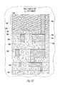
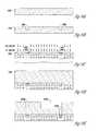
- FIG. 1illustrates relatively small pores 102 and metal lines 104 and 106 formed in an insulator 108 using a damascene process.
- the pores 102are smaller than the photo dimension of the lines 104 and 106 .
- the pores 102are formed before the metal is deposited, such that the metal 110 flows into some of the pores. However, the pores are small enough so that a short does not form between the metal lines.
- FIG. 2illustrates relatively large pores 202 and metal lines 204 and 206 formed in an insulator 208 using a damascene process. At least some of the pores 202 are larger than the photo dimension of the lines 204 and 206 . The pores are formed before the metal is deposited, such that the metal flows into some of the pores. The metal 210 is capable of flowing through a pore and forming a short between the metal lines.
- the present subject materrelates to improved interlayer dielectric (ILD) devices and methods of formation.
- ILDinterlayer dielectric
- the present subject matterprovides methods for forming voids in the ILD after the metal layer has been formed so as to alleviate the demands placed upon a process for producing a porous structure.
- the present subject matteris particularly useful as photolithographic dimensions continue to decrease.
- One aspect of the present subject matterrelates to a method for forming an interlayer dielectric (ILD).
- an insulatoris formed, at least one trench is formed in the insulator, and a metal layer is formed in the at least one trench.
- Voidsare formed in the insulator layer after the metal layer is formed.
- a multiphase matrixis formed as an insulator layer. At least one trench is formed in the insulator layer and a metal layer is then formed in the at least one trench. At least one phase is at least partially removed from the multiphase matrix to form voids in the insulator layer.
- an insulator layeris formed, at least one trench is formed in the insulator, and a metal layer is formed in the at least one trench.
- an inert gasis implanted and the insulator layer is annealed in an inert ambient to form a number of voids in the insulator layer.
- the integrated circuitincludes an insulator structure having a plurality of voids that have a maximum size, and a metal layer formed in the insulator structure.
- the metal layerhas a minimum photo dimension.
- the maximum size of the voidsis larger than the minimum photo dimension of the metal layer.
- a maximum-sized voidis capable of extending between a first metal line and a second metal line in the metal layer.
- FIG. 1illustrates relatively small pores and metal lines formed in a damascene process.
- FIG. 2illustrates relatively large pores and metal lines formed in a damascene process.
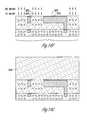
- FIG. 3illustrates an integrated circuit in which relatively large pores are formed after the metal lines are formed according to various embodiments of the present subject matter.
- FIG. 4illustrates a method for forming an interlayer dielectric (ILD) according to various embodiment of the present subject matter.
- ILDinterlayer dielectric
- FIG. 5illustrates a method for forming an ILD according to various embodiment of the present subject matter.
- FIG. 6illustrates a method for forming an ILD according to various embodiment of the present subject matter.
- FIG. 7illustrates a method for forming an ILD using a first process scheme according to various embodiments of the present subject matter.
- FIG. 8illustrates a method for forming an ILD using a first process scheme according to various embodiments of the present subject matter.
- FIG. 9illustrates a method for forming an ILD using a second process scheme according to various embodiments of the present subject matter.
- FIG. 10illustrates a method for creating a gas phase in an insulator structure according to various embodiments of the present subject matter.
- FIG. 11illustrates a method for creating a gas phase in an insulator structure according to various embodiments of the present subject matter.
- FIG. 12illustrates a method for forming an ILD using a second process scheme according to various embodiments of the present subject matter.
- FIGS. 13A through 13Iillustrate an example of forming an ILD using the first process scheme.
- FIGS. 14A through 14Iillustrate an example of forming an ILD using the second process scheme.
- FIG. 15is a simplified block diagram of a high-level organization of various embodiments of an electronic system according to the present subject matter.
- FIG. 16is a simplified block diagram of a high-level organization of various embodiments of an electronic system according to the present subject matter.
- the present subject matterintroduces micro-voids and/or nano-voids within a conventionally processed ILD (such as oxides, fluorinated oxide, SOG-HSQ and the like) to achieve K values in the range of 2-3 or lower without adversely affecting thermal and mechanical stability when the pores are formed after the film is deposited.
- ILDsuch as oxides, fluorinated oxide, SOG-HSQ and the like
- the present subject matterintroduces pores into the dielectric after the metal layer is defined, as illustrated below with respect to FIG. 3 .
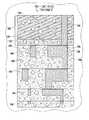
- FIG. 3illustrates an integrated circuit in which relatively large pores 302 are formed in the insulator 308 after the metal lines 304 and 306 are formed according to various embodiments of the present subject matter.
- the pores 302are capable of being larger than the photo dimension of the lines 304 and 306 because they are formed after the metal is deposited. As such, no short occurs even if the pores extend from one line to another line because air is a good insulator.
- the insulatoris a multi-phase structure. After the insulator is patterned, at least one of the phases is removed leaving the matrix phase intact. The intact matrix phase continues to provide structural rigidity and the spaces where the second (or multiple phases in the case of three phase or more complex structure) are now filled with air or other gas.
- a second process schemeintroduces a gas phase (e.g. an inert gas such as helium (He), argon (Ar), or nitrogen (N 2 )) into the insulator after it is in the solid state.
- the introduced gas phasealso can include air.
- an inert gase.g. He, Ar, N 2
- an inert gasis implanted into the post-processed insulator to create stable voids (microvoids or nanovoids) resulting in a two-phase insulator-gas (void) structure.
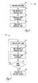
- FIG. 4illustrates a method for forming an interlayer dielectric (ILD) according to various embodiment of the present subject matter.
- an insulator layeris formed at 414 , trenches are formed in the insulator layer at 416 , and a metal layer is formed in the trenches at 418 .
- the insulator layeris formed from an inorganic material.
- the metal layeris appropriately connected to various devices to form an integrated circuit.
- voidsare formed in the insulator layer at 420 . Because the voids are formed after the metal layer is formed, the voids that are larger than the photo dimension of the metal layer will not cause a short between metal lines.
- FIG. 5illustrates a method for forming an ILD according to various embodiment of the present subject matter.
- an insulator layeris formed at 514
- trenchesare formed in the insulator layer at 516
- a metal layeris formed in the trenches at 518 .
- the processreturns to 514 if additional metal layers are to be formed.
- an ILD structure having more than one metal layeris capable of being formed.
- the processproceeds to 520 where voids are formed in one or more of the insulator layers. In this embodiment, voids are capable of being formed in more than one insulator layer after the last metal layer has been formed.
- FIG. 6illustrates a method for forming an ILD according to various embodiment of the present subject matter.
- an insulator layeris formed at 614 , trenches are formed in the insulator layer at 616 , and a metal layer is formed in the trenches at 618 .
- the processproceeds to 620 where voids are formed in the insulator layer.
- the processreturns to 614 if additional metal layers are to be formed.
- an ILD structure having more than one metal layeris capable of being formed.
- the voidsare formed after each metal layer is formed as the ILD structure is being built.
- voidsare capable of being formed in the first and second insulator layers after the second metal level is formed, are capable of being formed in the third insulator layer after the third metal level is formed, and are capable of being formed in the fourth insulator layer after the fourth metal level is formed.
- Process Scheme 1Remove Phase(s) from Multi-Phase Insulator Structure.
- FIG. 7illustrates a method for forming an ILD using a first process scheme according to various embodiments of the present subject matter.
- an insulator layer having a multiphase structureis formed at 714 , trenches are formed in the insulator layer at 716 , and a metal layer is formed in the trenches at 718 .
- voidsare formed in the insulator layer at 720 by removing (or partially removing) one or more phases from the multiphase structure. Because the voids are formed after the metal layer is formed, the voids that are larger than the photo dimension of the metal layer will not cause a short between metal lines.
- FIG. 8illustrates a method for forming an ILD using a first process scheme according to various embodiments of the present subject matter.
- an insulator having a multiphase structureis formed at 814 .
- a mixture of glass particles and carbon particlesis formed or otherwise provided at 822 .
- the glass particleshave a low-melting temperature, such as that provided by fritted glass.
- the carbon particlesare provided as graphite particles.
- the ratio of the carbon particles to the glass particlesis capable of being varied or selected to achieve a desired pore density.
- the particle size of the carbonis capable of being varied or selected according to the desired thickness of the insulator layer.
- the mixtureis heated to above the softening temperature of the glass until the glass flows and forms a continuous matrix phase that contains carbon particles.
- Metal linesare formed in the insulator using a damascene process. Trenches are formed in the insulator at 816 , and a metal layer is deposited in the trenches at 818 . At 820 , the resulting structure is exposed to a high temperature oxygen (O 2 ) containing environment. The oxygen diffuses through the glass matrix, oxidizes with carbon, and forms carbon dioxide (CO 2 ) voids in the insulator structure. Thus, the carbon phase of the multiphase structure is at least partially removed due to the diffusion of oxygen into the structure.
- the time of exposureis capable of being varied or selected at 830 , the temperature of the environment is capable of being varied or selected at 832 , and the O 2 concentration is capable of being varied or selected at 834 .
- the diffusion distance of the oxygen through the glass and between the carbon particlesis minimal because the maximum size of the carbon particles is equal to the thickness of the film to be formed such that many particles extend through the film.
- a rapid thermal annealis used in various embodiments to minimize the temperature exposure to the underlying device structure.
- the RTAincludes a laser anneal.
- the RTAincludes a plasma anneal.
- the elevated temperature of the environmentis in a range from 400 to 500° C., or in various sub-ranges within 400 to 500° C.
- Process Scheme 2Create Gas Phase in Insulator Structure.
- FIG. 9illustrates a method for forming an ILD using a second process scheme according to various embodiments of the present subject matter.
- an insulator layeris formed at 914
- trenchesare formed in the insulator layer at 916
- a metal layeris formed in the trenches at 918 .
- voidsare formed in the insulator layer at 920 by creating a gas phase in the insulator layer. Because the voids are formed after the metal layer is formed, the voids that are larger than the photo dimension of the metal layer will not cause a short between metal lines.
- FIG. 10illustrates a method for creating a gas phase in an insulator structure according to various embodiments of the present subject matter.
- the illustrated methodis represented as 1020 , and generally corresponds to element 920 in FIG. 9 .
- an inert gasis implanted into the insulator layer at 1036 , and the resulting structure is annealed at 1038 .
- FIG. 11illustrates a method for creating a gas phase in an insulator structure according to various embodiments of the present subject matter.
- the illustrated methodis represented as 1120 , and generally corresponds to element 920 in FIG. 9 .
- heliumHe
- Arargon
- N 2nitrogen
- Heliumis used herein to simplify the disclosure.
- Voidssuch as nano-voids, are formed when implant induced vacancies and helium migrate and combine during the post-implant anneal.
- FIG. 12illustrates a method for forming an ILD using a second process scheme according to various embodiments of the present subject matter.
- the illustrated methodis represented as 1220 , and generally corresponds to element 920 in FIG. 9 .
- heliumHe
- the resulting structureis annealed at 1238 .
- the size and distribution of the voidsare capable of being controlled by varying or selecting an implant dose at 1240 and an implant energy at 1242 .
- Stable geometriesare capable of being obtained by appropriately varying or selecting the post-implant annealing parameters, such as temperature at 1246 , time at 1248 , ambient (such as He, N 2 , Ar and the like) at 1250 , annealing tools at 1252 , and annealing methodology at 1254 .
- a heavy dose of an inert gasis implanted in the processed insulator, and the resulting structure is annealed.
- an inert gasis implanted in the processed insulator, and the resulting structure is annealed.
- a dose of helium (He) in excess of 2 ⁇ 10 15 /cm 2is implanted.
- Stable nano-cavities or nano-voidsare generated inside of the ILD material. The voids are formed when implant induced vacancies and helium migrate and combine during the post-implant anneal.
- the size and distribution of these voidsare capable of being varied by varying the implant dose.
- Stable geometriesare capable of being obtained by optimizing the post-implant annealing parameters, such as annealing temperature, time, ambient, annealing tools, and methodology.
- Multiple layers of these nanovoidsare capable of being formed and stabilized by successive implants at different implant energies by placing helium and vacancy clusters at different depths of the material in which helium is ion implanted and the material is appropriately annealed.
- Multiple layers of nano-voidsare capable of being generated by implanting the inert gas at different depths of ILD by varying the implant energy and adjusting the dose and annealing tools and parameters. It has been shown that single and multiple layers of stable micro/nano cavities can be formed in silicon material by implanting a dose of helium greater than or equal to 2 ⁇ 10 15 at different implant energies followed by an appropriate anneal in an inert ambient. Stable multiple layers of spherical cavities, of 10 to 90 nm in diameters of similar shape, have been formed in silicon within the layer. The distance of separation between layers is from 110 nm to 120 nm.
- the ILD layeris first produced by a back-end-of-line (BEOL) processing of silicon technology.
- BEOLback-end-of-line
- a first layer of voids (helium or other ions) and associated vacancy cluster)is generated at a desired depth by appropriately selecting the dose and energy of the helium implant.
- the implanted structureis annealed in an inert ambient with an appropriate thermal budget (e.g. time, temperature and the like) to control and stabilize the geometry and distribution of the voids.
- the inert ambientincludes nitrogen.
- the inert ambientincludes argon.
- the thermal budgetis contained and controlled by using appropriate rapid thermal annealing. In various embodiments, the thermal budget is contained and controlled by using laser pulse annealing. In various embodiments, the thermal budget is contained and controlled by using plasma annealing at a relatively low temperature.
- stable voidsare capable of being formed at a desired depth inside the ILD material by repeating the implant and annealing with an appropriate implant energy.
- a stable void fraction of greater than 0.5is capable of being readily targeted within a SiO 2 ILD layer.
- An effective K value of ILD less than or equal to 1.5is capable of being achieved by incorporating stable nan-voids in SiO 2 ILD. Therefore inter and intra-layer capacitance of BEOL interconnects are capable of being dramatically reduced and chip performance is capable of being significantly improved.
- the first and second metal levels of the structureare to have a minimum photolithographic dimension of 0.3 microns and a thickness of 0.6 microns.
- the third and fourth metal levels of the structureare to have a minimum photolithographic dimension of 0.7 micron and a metal thickness of 1.5 microns.
- the insulator thickness between the first and second metal levels as well as between the second and third metal levelsis to be approximately 0.75 microns.
- the insulator thickness between the third and fourth metal levelsis to be approximately 1.5 microns thick.
- Each insulator layeris to be formed with a pore density of 40 percent voids.
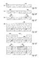
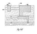
- FIGS. 13A through 13Iillustrate an example of forming an ILD using the first process scheme.
- a mixture of low melting point glass particles and carbon particlesis deposited to form a first layer 1356 , as shown in FIG. 13 A.
- the carbon particles 1358form about 40% of the mixture, and corresponds generally to the desired pore density of 40% voids.
- the maximum particle size of the carbonis about 0.6 microns.
- the first layer of the mixtureis heated such that the glass particles flow, resulting in a first insulator layer of carbon-containing glass that is 0.6 microns thick.
- the thickness of the glassgenerally corresponds to the maximum size of the carbon particles.
- Trenches 1360are cut into the film 1356 in FIG. 13 B.
- the liner and copper layer 1362are deposited and planarized to form the metal layer.
- a capping layer 1364is applied using a process as described by Farrar in the following commonly assigned U.S. patent application which is herein incorporated by reference in its entirety: “Method Of Fabricating A Barrier Layer On Top Surfaces Of Metals In Damascene Structures,” Ser. No. 09/534,224, filed on Mar. 24, 2000. In this process the capping layer remains only on the metal surface so that the upper surface of the intralayer dielectric is not covered.
- a second layer 1366 of insulator slurry with a maximum carbon particle 1368 of 1.35 micronsis applied to form a carbon-containing 1.35 micron insulator layer, as shown in FIG. 13 D.
- the insulator layer 1366is etched to provide a dual damascene trench 1370 A and 1370 B for the 0.6 micron second level metallurgy 1370 A and the via structure 1370 B for first to second level vias.
- the second level metallurgyis deposited using a similar process to that used in forming the first level metallurgy, so as to provide a liner and copper layer 1372 and a capping layer 1374 .
- a third layer 1376 of insulating slurry with a maximum carbon particle 1378 size of 2.5 micronsis deposited, forming a 2.5 micron insulator film.
- This insulator filmis etched to form a dual damascene trench and for the 1.5 micron thick third level metallurgy and the 0.75 micron second to third level vias.
- the metallurgyis formed using a similar process as was used for the lower metal levels, so as to provide a liner and copper layer 1380 and a capping layer 1382 .
- a fourth layer 1384 of insulating slurry with a maximum particle size of 3 micronsis deposited, forming a 3 micron insulator film.
- This insulator filmis etched to form a dual damascene structure for the 1.5 micron thick third level metallurgy and the 1.5 micron third to fourth level vias.
- the metallurgyis formed using a similar process as was used for the lower metal levels, so as to provide a liner and copper layer 1386 and a capping layer 1388 .
- the carbonis removed by exposing the film to an oxygen-containing ambient at an elevated temperature, resulting in CO 2 voids 1390 in the insulator structure.
- the elevated temperatureis approximately 450° C.
- the elevated temperatureis within a range from 400 to 500° C.
- the elevated temperatureis within various subranges within the range from 400 to 500° C.
- the maximum particle size of the carbon particlesis equal to the thickness of the insulator film to be formed. Thus, there are many particles that will extend through the film in each layer. Consequently, the diffusion distance of oxygen through the glass and between the carbon particles is minimal.
- a rapid thermal anneal (RTA) processis used to minimize the temperature exposure to the underlying device structure.
- RTArapid thermal anneal
- a final passivation layer 1392is capable of being built in a number of processes depending upon specific system requirements.
- Various embodimentuse a 0.5 micron carbon glass layer 1394 which is deposited prior to the removal of the carbon in the lower composited films. The carbon is removed from this film at the same time as the rest of the structure.
- a 4 micron layer of Polyimide 1396is applied as the final insulating layer. Vias 1398 are formed in the composite layer so that the terminal metallurgy can be connected.
- the voidsare formed by first etching the glass layer prior to the Polyimide layer being applied.
- the voidsare formed after the Polyimide is applied. The use of a thin composite layer under the thick Polyimide (which is highly viscose when applied), ensures that little if any Polyimide is able to fill the voids created between the fourth level metal lines.
- FIGS. 14A through 14Iillustrate an example of forming an ILD using the second process scheme.
- the insulator usedhas a density similar to SiO 2 .
- the insulatorsuch as glass
- the insulatorcan have a different density and ion stopping power such that different implant energies are required.
- the required over pressureis dependent on the softening point of the glass as well as the chosen annealing temperature.
- an insulatoris deposited to form a 0.6 micron first insulator layer 1456 .
- the oxideis selected such that the softening point of the oxide is well below the melting point of the metal to be used for the conductors, and is preferably below 475 to 500° C. If a high temperature metallurgy, such as tungsten, is used, the limiting temperature is determined by the temperature that is compatible with the thermal budget of the device structure.
- trenches 1460 of 0.3 microns wideare etched into the oxide and the liner, copper metallurgy 1462 and capping layer 1464 are formed using the same process as in the first example.
- a first implant of heliumhas a dose of about 5 ⁇ 10 15 /cm 2 at an implant energy of about 10 KEV.
- a second implanthas a dose of about 5 ⁇ 10 15 /cm 2 at an implant energy of about 45 KEV.
- These two implantsprovide sufficient helium (He) to form 40 percent voids with about a 50 percent excess helium to allow for over pressure and helium loss during processing.
- the structureis annealed using a RTA process at a temperature and for a time sufficient to form the voids 1490 . In various embodiments, the annealing temperature is within the range of 400 to 500° C.
- the annealing temperatureincludes various sub-ranges within the range of 400 to 500° C.
- the height of the oxide spacersis increased by approximately 40%.
- CMPchemical mechanical polishing
- a layer 1466 of oxide approximately 0.75 microns thickis applied followed by a touch-up CMP process to planarize the surface.
- the process described aboveis implemented to form trenches 1470 A for the metallurgy 1472 and trenches 1470 B for the first to second level vias.
- the ion-implantsare 7.510 15 /cm 2 at 25 KEV and 7.510 15 /cm 2 at 70 KEV.
- the structureis annealed at 400 to 500° C. until approximately 40% voids 1490 are formed.
- a CMP processis performed, as in the previous step.
- an oxide film approximately 0.6 microns thickis applied, and the sequence of steps used to form the first level of metal are repeated to form the second level of metal 1480 and capping layer 1482 as shown in FIG. 14 H.
- An oxide film approximately 0.75 microns thickis applied with processing similar to the first 0.75 micron film to form the second to third level via structure.
- a 1.5 micron film 1484is deposited and patterned to form the troughs for the third metal level 1486 and capping layer 1488 .
- the metalis deposited and patterned using a process similar to that for the first two levels except for the greater metal thickness. Implants of 7.510 15 /cm 2 at 45, 90, 170 and 280 KEV are performed, and the structure is annealed. The excess oxide is removed again leaving the capping layer on the metallurgy undisturbed. This process is repeated to form the third to fourth level vias structures and the fourth metal level.
- the final layer of oxide 1494approximately 0.5 micron thick and the Polyimide layer 1496 are deposited and terminal vias 1498 are etched.
- a single damascene processis used in contrast to the dual damascene process used in the first process illustrated above.
- a dual damascene processmay exert too high a stress on the metal layers being formed because of the swelling which occurs during the formation of the vias. However, if the process to form the pores is run at a temperature sufficiently high, the glass flows sufficiently to provide a low stress. Thus, in various embodiments which use a relatively low melting glass and a high temperature metal such as tungsten, a dual damascene process is capable of being used.
- FIG. 15is a simplified block diagram of a high-level organization of various embodiments of an electronic system according to the present subject matter.
- the system 1500is a computer system, a process control system or other system that employs a processor and associated memory.
- the electronic system 1500has functional elements, including a processor or arithmetic/logic unit (ALU) 1502 , a control unit 1504 , a memory device unit 1506 and an input/output (I/O) device 1508 .
- ALUarithmetic/logic unit
- the control unit 1504coordinates all operations of the processor 1502 , the memory device 1506 and the I/O devices 1508 by continuously cycling through a set of operations that cause instructions to be fetched from the memory device 1506 and executed.
- the memory device 1506includes, but is not limited to, random access memory (RAM) devices, read-only memory (ROM) devices, and peripheral devices such as a floppy disk drive and a compact disk CD-ROM drive.
- RAMrandom access memory
- ROMread-only memory
- peripheral devicessuch as a floppy disk drive and a compact disk CD-ROM drive.
- FIG. 16is a simplified block diagram of a high-level organization of various embodiments of an electronic system according to the present subject matter.
- the system 1600includes a memory device 1602 which has an array of memory cells 1604 , address decoder 1606 , row access circuitry 1608 , column access circuitry 1610 , control circuitry 1612 for controlling operations, and input/output circuitry 1614 .
- the memory device 1602further includes power circuitry 1616 , a charge pump 1618 for providing the higher-voltage programming pulses, and sensors 1620 such as current sensors for determining whether a memory cell is in a low-threshold conducting state or in a high-threshold nonconducting state. Also, as shown in FIG.
- the system 1600includes a processor 1622 , or memory controller for memory accessing.
- the memory device 1602receives control signals 1624 from the processor 1622 over wiring or metallization lines.
- the memory device 1602is used to store data which is accessed via I/O lines. It will be appreciated by those skilled in the art that additional circuitry and control signals can be provided, and that the memory device 1602 has been simplified to help focus on the invention. At least one of the processor 1622 or memory device 1602 has the low-K ILD according to the present subject matter.
- FIG. 16The illustration of system, as shown in FIG. 16 , is intended to provide a general understanding of one application for the structure and circuitry of the present subject matter, and is not intended to serve as a complete description of all the elements and features of an electronic system using low-K ILD according to the present subject matter.
- an electronic systemcan be fabricated in single-package processing units, or even on a single semiconductor chip, in order to reduce the communication time between the processor and the memory device.
- Applications containing the low-K ILD as described in this disclosureinclude electronic systems for use in memory modules, device drivers, power modules, communication modems, processor modules, and application-specific modules, and may include multilayer, multichip modules.
- Such circuitrycan further be a subcomponent of a variety of electronic systems, such as a clock, a television, a cell phone, a personal computer, an automobile, an industrial control system, an aircraft, and others.
- the present subject materrelates to improved interlayer dielectric (ILD) devices and methods of formation.
- the present subject matterprovides methods for forming voids in the ILD after the metal layer has been formed so as to alleviate the demands placed upon a process for producing a porous structure.
- the present subject matteris particularly useful as photolithographic dimensions continue to decrease.
- the insulatoris a multi-phase structure. After the insulator is patterned, at least one of the phases is removed leaving the matrix phase intact. The intact matrix phase continues to provide structural rigidity and the spaces where the second (or multiple phases in the case of three phase or more complex structure) are now filled with air or other gas.
- a second process schemeintroduces a gas phase (e.g. an inert gas such as helium (He), argon (Ar), or nitrogen (N 2 )) into the insulator after it is in the solid state.
- the introduced gas phasealso can include air.
Landscapes
- Engineering & Computer Science (AREA)
- Physics & Mathematics (AREA)
- Condensed Matter Physics & Semiconductors (AREA)
- General Physics & Mathematics (AREA)
- Computer Hardware Design (AREA)
- Microelectronics & Electronic Packaging (AREA)
- Power Engineering (AREA)
- Manufacturing & Machinery (AREA)
- Plasma & Fusion (AREA)
- Internal Circuitry In Semiconductor Integrated Circuit Devices (AREA)
Abstract
Description
Claims (23)
Priority Applications (4)
| Application Number | Priority Date | Filing Date | Title |
|---|---|---|---|
| US10/198,586US6903001B2 (en) | 2002-07-18 | 2002-07-18 | Techniques to create low K ILD for BEOL |
| US10/931,182US7157387B2 (en) | 2002-07-18 | 2004-08-31 | Techniques to create low K ILD for BEOL |
| US10/931,140US7190043B2 (en) | 2002-07-18 | 2004-08-31 | Techniques to create low K ILD for beol |
| US11/493,335US7492030B2 (en) | 2002-07-18 | 2006-07-26 | Techniques to create low K ILD forming voids between metal lines |
Applications Claiming Priority (1)
| Application Number | Priority Date | Filing Date | Title |
|---|---|---|---|
| US10/198,586US6903001B2 (en) | 2002-07-18 | 2002-07-18 | Techniques to create low K ILD for BEOL |
Related Child Applications (2)
| Application Number | Title | Priority Date | Filing Date |
|---|---|---|---|
| US10/931,182DivisionUS7157387B2 (en) | 2002-07-18 | 2004-08-31 | Techniques to create low K ILD for BEOL |
| US10/931,140DivisionUS7190043B2 (en) | 2002-07-18 | 2004-08-31 | Techniques to create low K ILD for beol |
Publications (2)
| Publication Number | Publication Date |
|---|---|
| US20040014273A1 US20040014273A1 (en) | 2004-01-22 |
| US6903001B2true US6903001B2 (en) | 2005-06-07 |
Family
ID=30443144
Family Applications (4)
| Application Number | Title | Priority Date | Filing Date |
|---|---|---|---|
| US10/198,586Expired - LifetimeUS6903001B2 (en) | 2002-07-18 | 2002-07-18 | Techniques to create low K ILD for BEOL |
| US10/931,182Expired - LifetimeUS7157387B2 (en) | 2002-07-18 | 2004-08-31 | Techniques to create low K ILD for BEOL |
| US10/931,140Expired - LifetimeUS7190043B2 (en) | 2002-07-18 | 2004-08-31 | Techniques to create low K ILD for beol |
| US11/493,335Expired - LifetimeUS7492030B2 (en) | 2002-07-18 | 2006-07-26 | Techniques to create low K ILD forming voids between metal lines |
Family Applications After (3)
| Application Number | Title | Priority Date | Filing Date |
|---|---|---|---|
| US10/931,182Expired - LifetimeUS7157387B2 (en) | 2002-07-18 | 2004-08-31 | Techniques to create low K ILD for BEOL |
| US10/931,140Expired - LifetimeUS7190043B2 (en) | 2002-07-18 | 2004-08-31 | Techniques to create low K ILD for beol |
| US11/493,335Expired - LifetimeUS7492030B2 (en) | 2002-07-18 | 2006-07-26 | Techniques to create low K ILD forming voids between metal lines |
Country Status (1)
| Country | Link |
|---|---|
| US (4) | US6903001B2 (en) |
Cited By (7)
| Publication number | Priority date | Publication date | Assignee | Title |
|---|---|---|---|---|
| US20020082936A1 (en)* | 2000-12-21 | 2002-06-27 | Nokia Corporation | Simulated speed-of-light delay for recreational benefit applications |
| US20050236714A1 (en)* | 2002-11-21 | 2005-10-27 | Jihperng Leu | Selectively converted inter-layer dielectric |
| US20060102957A1 (en)* | 2004-11-12 | 2006-05-18 | Jhon-Jhy Liaw | SER immune cell structure |
| US20070096319A1 (en)* | 2005-11-03 | 2007-05-03 | International Business Machines Corporation | Method for fabricating and BEOL interconnect structures with simultaneous formation of high-k and low-k dielectric regions |
| US20070278693A1 (en)* | 2006-05-31 | 2007-12-06 | Matthias Lehr | Metallization layer of a semiconductor device having differently thick metal lines and a method of forming the same |
| US20100078814A1 (en)* | 2008-09-29 | 2010-04-01 | Roy Alok Nandini | System and method for using porous low dielectric films |
| US20160163594A1 (en)* | 2012-12-26 | 2016-06-09 | SK Hynix Inc. | Method for forming void-free polysilicon and method for fabricating semiconductor device using the same |
Families Citing this family (15)
| Publication number | Priority date | Publication date | Assignee | Title |
|---|---|---|---|---|
| US6903001B2 (en)* | 2002-07-18 | 2005-06-07 | Micron Technology Inc. | Techniques to create low K ILD for BEOL |
| US7005371B2 (en)* | 2004-04-29 | 2006-02-28 | International Business Machines Corporation | Method of forming suspended transmission line structures in back end of line processing |
| US7223670B2 (en) | 2004-08-20 | 2007-05-29 | International Business Machines Corporation | DUV laser annealing and stabilization of SiCOH films |
| US7229909B2 (en)* | 2004-12-09 | 2007-06-12 | International Business Machines Corporation | Integrated circuit chip utilizing dielectric layer having oriented cylindrical voids formed from carbon nanotubes |
| US7382012B2 (en)* | 2006-02-24 | 2008-06-03 | Taiwan Semiconductor Manufacturing Company, Ltd. | Reducing parasitic capacitance of MIM capacitor in integrated circuits by reducing effective dielectric constant of dielectric layer |
| KR100900231B1 (en)* | 2007-06-21 | 2009-06-02 | 주식회사 하이닉스반도체 | Manufacturing method of semiconductor device |
| WO2010082250A1 (en)* | 2009-01-13 | 2010-07-22 | パナソニック株式会社 | Semiconductor device and method for manufacturing same |
| US7807570B1 (en) | 2009-06-11 | 2010-10-05 | International Business Machines Corporation | Local metallization and use thereof in semiconductor devices |
| US8358007B2 (en)* | 2009-06-11 | 2013-01-22 | Globalfoundries Singapore Pte. Ltd. | Integrated circuit system employing low-k dielectrics and method of manufacture thereof |
| JP5351201B2 (en)* | 2011-03-25 | 2013-11-27 | 株式会社東芝 | Nonvolatile semiconductor memory device and manufacturing method thereof |
| US9564355B2 (en)* | 2013-12-09 | 2017-02-07 | Taiwan Semiconductor Manufacturing Company, Ltd. | Interconnect structure for semiconductor devices |
| US9613906B2 (en)* | 2014-06-23 | 2017-04-04 | GlobalFoundries, Inc. | Integrated circuits including modified liners and methods for fabricating the same |
| US9773866B2 (en) | 2015-06-18 | 2017-09-26 | Qualcomm Incorporated | Semiconductor integrated circuits (ICs) employing localized low dielectric constant (low-K) material in inter-layer dielectric (ILD) material for improved speed performance |
| KR20190071227A (en)* | 2017-12-14 | 2019-06-24 | 에스케이하이닉스 주식회사 | Electronic device and method for fabricating the same |
| US11114335B1 (en)* | 2020-04-14 | 2021-09-07 | Nanya Technology Corporation | Semiconductor device structure with air gap structure and method for forming the same |
Citations (19)
| Publication number | Priority date | Publication date | Assignee | Title |
|---|---|---|---|---|
| US4962058A (en) | 1989-04-14 | 1990-10-09 | International Business Machines Corporation | Process for fabricating multi-level integrated circuit wiring structure from a single metal deposit |
| US6077792A (en) | 1997-07-14 | 2000-06-20 | Micron Technology, Inc. | Method of forming foamed polymeric material for an integrated circuit |
| US6100176A (en) | 1998-02-25 | 2000-08-08 | Micron Technology, Inc. | Methods and structures for gold interconnections in integrated circuits |
| US6150257A (en) | 1998-08-28 | 2000-11-21 | Micron Technology, Inc. | Plasma treatment of an interconnect surface during formation of an interlayer dielectric |
| US6387824B1 (en)* | 1999-01-27 | 2002-05-14 | Matsushita Electric Industrial Co., Ltd. | Method for forming porous forming film wiring structure |
| US6395647B1 (en) | 1999-09-02 | 2002-05-28 | Micron Technology, Inc. | Chemical treatment of semiconductor substrates |
| US6413827B2 (en) | 2000-02-14 | 2002-07-02 | Paul A. Farrar | Low dielectric constant shallow trench isolation |
| US6420262B1 (en) | 2000-01-18 | 2002-07-16 | Micron Technology, Inc. | Structures and methods to enhance copper metallization |
| US20020168872A1 (en) | 1999-08-25 | 2002-11-14 | Micron Technology, Inc. | Insulators for high density circuits |
| US6509590B1 (en) | 1998-07-20 | 2003-01-21 | Micron Technology, Inc. | Aluminum-beryllium alloys for air bridges |
| US20030015781A1 (en) | 2001-07-19 | 2003-01-23 | Farrar Paul A. | Method of using foamed insulators in three dimensional multichip structures |
| US6522011B1 (en) | 2000-08-15 | 2003-02-18 | Micron Technology, Inc. | Low capacitance wiring layout and method for making same |
| US6534835B2 (en) | 2000-08-28 | 2003-03-18 | Micron Technology, Inc. | Damascene structure with low dielectric constant insulating layers |
| US6541859B1 (en) | 1998-02-25 | 2003-04-01 | Micron Technology, Inc. | Methods and structures for silver interconnections in integrated circuits |
| US6617239B1 (en) | 2000-08-31 | 2003-09-09 | Micron Technology, Inc. | Subtractive metallization structure and method of making |
| US20030181018A1 (en) | 2002-03-25 | 2003-09-25 | Micron Technology, Inc. | Low k interconnect dielectric using surface transformation |
| US6630403B2 (en) | 1999-02-16 | 2003-10-07 | Micron Technology, Inc. | Reduction of surface roughness during chemical mechanical planarization (CMP) |
| US6649522B2 (en) | 2000-08-31 | 2003-11-18 | Micron Technology, Inc. | Etch stop in damascene interconnect structure and method of making |
| US6677209B2 (en) | 2000-02-14 | 2004-01-13 | Micron Technology, Inc. | Low dielectric constant STI with SOI devices |
Family Cites Families (75)
| Publication number | Priority date | Publication date | Assignee | Title |
|---|---|---|---|---|
| US5946553A (en)* | 1991-06-04 | 1999-08-31 | Micron Technology, Inc. | Process for manufacturing a semiconductor package with bi-substrate die |
| US5252857A (en)* | 1991-08-05 | 1993-10-12 | International Business Machines Corporation | Stacked DCA memory chips |
| KR940008327B1 (en)* | 1991-10-10 | 1994-09-12 | 삼성전자 주식회사 | Semiconductor package and its mounting method |
| US5128831A (en)* | 1991-10-31 | 1992-07-07 | Micron Technology, Inc. | High-density electronic package comprising stacked sub-modules which are electrically interconnected by solder-filled vias |
| US5593927A (en)* | 1993-10-14 | 1997-01-14 | Micron Technology, Inc. | Method for packaging semiconductor dice |
| US5461003A (en)* | 1994-05-27 | 1995-10-24 | Texas Instruments Incorporated | Multilevel interconnect structure with air gaps formed between metal leads |
| US5847464A (en)* | 1995-09-27 | 1998-12-08 | Sgs-Thomson Microelectronics, Inc. | Method for forming controlled voids in interlevel dielectric |
| US5835987A (en)* | 1995-10-31 | 1998-11-10 | Micron Technology, Inc. | Reduced RC delay between adjacent substrate wiring lines |
| US6013948A (en)* | 1995-11-27 | 2000-01-11 | Micron Technology, Inc. | Stackable chip scale semiconductor package with mating contacts on opposed surfaces |
| US5851845A (en)* | 1995-12-18 | 1998-12-22 | Micron Technology, Inc. | Process for packaging a semiconductor die using dicing and testing |
| US5719440A (en)* | 1995-12-19 | 1998-02-17 | Micron Technology, Inc. | Flip chip adaptor package for bare die |
| US6072236A (en)* | 1996-03-07 | 2000-06-06 | Micron Technology, Inc. | Micromachined chip scale package |
| US6072324A (en)* | 1996-03-19 | 2000-06-06 | Micron Technology, Inc. | Method for testing semiconductor packages using oxide penetrating test contacts |
| JP2806357B2 (en)* | 1996-04-18 | 1998-09-30 | 日本電気株式会社 | Stack module |
| DE19626126C2 (en)* | 1996-06-28 | 1998-04-16 | Fraunhofer Ges Forschung | Method for forming a spatial chip arrangement and spatial chip arrangement |
| KR100222299B1 (en)* | 1996-12-16 | 1999-10-01 | 윤종용 | Wafer level chip scale package and method of manufacturing the same |
| US5907769A (en)* | 1996-12-30 | 1999-05-25 | Micron Technology, Inc. | Leads under chip in conventional IC package |
| US5834945A (en)* | 1996-12-31 | 1998-11-10 | Micron Technology, Inc. | High speed temporary package and interconnect for testing semiconductor dice and method of fabrication |
| US5994166A (en)* | 1997-03-10 | 1999-11-30 | Micron Technology, Inc. | Method of constructing stacked packages |
| US6271582B1 (en)* | 1997-04-07 | 2001-08-07 | Micron Technology, Inc. | Interdigitated leads-over-chip lead frame, device, and method for supporting an integrated circuit die |
| US5986209A (en)* | 1997-07-09 | 1999-11-16 | Micron Technology, Inc. | Package stack via bottom leaded plastic (BLP) packaging |
| US6107122A (en)* | 1997-08-04 | 2000-08-22 | Micron Technology, Inc. | Direct die contact (DDC) semiconductor package |
| US6085962A (en)* | 1997-09-08 | 2000-07-11 | Micron Technology, Inc. | Wire bond monitoring system for layered packages |
| US5891797A (en)* | 1997-10-20 | 1999-04-06 | Micron Technology, Inc. | Method of forming a support structure for air bridge wiring of an integrated circuit |
| US6097087A (en)* | 1997-10-31 | 2000-08-01 | Micron Technology, Inc. | Semiconductor package including flex circuit, interconnects and dense array external contacts |
| US6437586B1 (en)* | 1997-11-03 | 2002-08-20 | Micron Technology, Inc. | Load board socket adapter and interface method |
| US6018249A (en)* | 1997-12-11 | 2000-01-25 | Micron Technolgoy, Inc. | Test system with mechanical alignment for semiconductor chip scale packages and dice |
| US6175149B1 (en)* | 1998-02-13 | 2001-01-16 | Micron Technology, Inc. | Mounting multiple semiconductor dies in a package |
| US6297547B1 (en)* | 1998-02-13 | 2001-10-02 | Micron Technology Inc. | Mounting multiple semiconductor dies in a package |
| US6429528B1 (en)* | 1998-02-27 | 2002-08-06 | Micron Technology, Inc. | Multichip semiconductor package |
| US6028365A (en)* | 1998-03-30 | 2000-02-22 | Micron Technology, Inc. | Integrated circuit package and method of fabrication |
| US5933713A (en)* | 1998-04-06 | 1999-08-03 | Micron Technology, Inc. | Method of forming overmolded chip scale package and resulting product |
| US6089920A (en)* | 1998-05-04 | 2000-07-18 | Micron Technology, Inc. | Modular die sockets with flexible interconnects for packaging bare semiconductor die |
| US6072233A (en)* | 1998-05-04 | 2000-06-06 | Micron Technology, Inc. | Stackable ball grid array package |
| US5990566A (en)* | 1998-05-20 | 1999-11-23 | Micron Technology, Inc. | High density semiconductor package |
| US6008070A (en)* | 1998-05-21 | 1999-12-28 | Micron Technology, Inc. | Wafer level fabrication and assembly of chip scale packages |
| US6020629A (en)* | 1998-06-05 | 2000-02-01 | Micron Technology, Inc. | Stacked semiconductor package and method of fabrication |
| US6153929A (en)* | 1998-08-21 | 2000-11-28 | Micron Technology, Inc. | Low profile multi-IC package connector |
| KR100269540B1 (en)* | 1998-08-28 | 2000-10-16 | 윤종용 | Method for manufacturing chip scale packages at wafer level |
| US6281042B1 (en)* | 1998-08-31 | 2001-08-28 | Micron Technology, Inc. | Structure and method for a high performance electronic packaging assembly |
| TW395025B (en) | 1998-09-03 | 2000-06-21 | United Microelectronics Corp | Manufacturing method of the unlanded via plug |
| US6214716B1 (en)* | 1998-09-30 | 2001-04-10 | Micron Technology, Inc. | Semiconductor substrate-based BGA interconnection and methods of farication same |
| US6208030B1 (en)* | 1998-10-27 | 2001-03-27 | Advanced Micro Devices, Inc. | Semiconductor device having a low dielectric constant material |
| US6184465B1 (en)* | 1998-11-12 | 2001-02-06 | Micron Technology, Inc. | Semiconductor package |
| US6232666B1 (en)* | 1998-12-04 | 2001-05-15 | Mciron Technology, Inc. | Interconnect for packaging semiconductor dice and fabricating BGA packages |
| US6656822B2 (en)* | 1999-06-28 | 2003-12-02 | Intel Corporation | Method for reduced capacitance interconnect system using gaseous implants into the ILD |
| US6228687B1 (en)* | 1999-06-28 | 2001-05-08 | Micron Technology, Inc. | Wafer-level package and methods of fabricating |
| US6556962B1 (en)* | 1999-07-02 | 2003-04-29 | Intel Corporation | Method for reducing network costs and its application to domino circuits |
| KR100298827B1 (en)* | 1999-07-09 | 2001-11-01 | 윤종용 | Method For Manufacturing Wafer Level Chip Scale Packages Using Redistribution Substrate |
| US6239489B1 (en)* | 1999-07-30 | 2001-05-29 | Micron Technology, Inc. | Reinforcement of lead bonding in microelectronics packages |
| US6709968B1 (en)* | 2000-08-16 | 2004-03-23 | Micron Technology, Inc. | Microelectronic device with package with conductive elements and associated method of manufacture |
| US6294839B1 (en)* | 1999-08-30 | 2001-09-25 | Micron Technology, Inc. | Apparatus and methods of packaging and testing die |
| US6212767B1 (en)* | 1999-08-31 | 2001-04-10 | Micron Technology, Inc. | Assembling a stacked die package |
| US6303981B1 (en)* | 1999-09-01 | 2001-10-16 | Micron Technology, Inc. | Semiconductor package having stacked dice and leadframes and method of fabrication |
| US6888247B2 (en)* | 1999-09-03 | 2005-05-03 | United Microelectronics Corp. | Interconnect structure with an enlarged air gaps disposed between conductive structures or surrounding a conductive structure within the same |
| JP2001196372A (en)* | 2000-01-13 | 2001-07-19 | Mitsubishi Electric Corp | Semiconductor device |
| US6326698B1 (en)* | 2000-06-08 | 2001-12-04 | Micron Technology, Inc. | Semiconductor devices having protective layers thereon through which contact pads are exposed and stereolithographic methods of fabricating such semiconductor devices |
| US6560117B2 (en)* | 2000-06-28 | 2003-05-06 | Micron Technology, Inc. | Packaged microelectronic die assemblies and methods of manufacture |
| US6552910B1 (en)* | 2000-06-28 | 2003-04-22 | Micron Technology, Inc. | Stacked-die assemblies with a plurality of microelectronic devices and methods of manufacture |
| US6407381B1 (en)* | 2000-07-05 | 2002-06-18 | Amkor Technology, Inc. | Wafer scale image sensor package |
| US6503780B1 (en)* | 2000-07-05 | 2003-01-07 | Amkor Technology, Inc. | Wafer scale image sensor package fabrication method |
| US6524944B1 (en)* | 2000-07-17 | 2003-02-25 | Advanced Micro Devices, Inc. | Low k ILD process by removable ILD |
| US6483044B1 (en)* | 2000-08-23 | 2002-11-19 | Micron Technology, Inc. | Interconnecting substrates for electrical coupling of microelectronic components |
| US6607937B1 (en)* | 2000-08-23 | 2003-08-19 | Micron Technology, Inc. | Stacked microelectronic dies and methods for stacking microelectronic dies |
| US6413852B1 (en)* | 2000-08-31 | 2002-07-02 | International Business Machines Corporation | Method of forming multilevel interconnect structure containing air gaps including utilizing both sacrificial and placeholder material |
| EP1323189A2 (en)* | 2000-09-13 | 2003-07-02 | Shipley Company LLC | Electronic device manufacture |
| US6451712B1 (en)* | 2000-12-18 | 2002-09-17 | International Business Machines Corporation | Method for forming a porous dielectric material layer in a semiconductor device and device formed |
| SG118084A1 (en)* | 2001-08-24 | 2006-01-27 | Micron Technology Inc | Method and apparatus for cutting semiconductor wafers |
| US6548376B2 (en)* | 2001-08-30 | 2003-04-15 | Micron Technology, Inc. | Methods of thinning microelectronic workpieces |
| US6537896B1 (en)* | 2001-12-04 | 2003-03-25 | Lsi Logic Corporation | Process for treating porous low k dielectric material in damascene structure to form a non-porous dielectric diffusion barrier on etched via and trench surfaces in the porous low k dielectric material |
| US6682357B2 (en)* | 2002-03-21 | 2004-01-27 | Dekko Stamping | Electrical terminal connector |
| US6774057B1 (en)* | 2002-06-25 | 2004-08-10 | Lsi Logic Corporation | Method and structure for forming dielectric layers having reduced dielectric constants |
| US6903001B2 (en)* | 2002-07-18 | 2005-06-07 | Micron Technology Inc. | Techniques to create low K ILD for BEOL |
| US20050104171A1 (en)* | 2003-11-13 | 2005-05-19 | Benson Peter A. | Microelectronic devices having conductive complementary structures and methods of manufacturing microelectronic devices having conductive complementary structures |
| US7091124B2 (en)* | 2003-11-13 | 2006-08-15 | Micron Technology, Inc. | Methods for forming vias in microelectronic devices, and methods for packaging microelectronic devices |
- 2002
- 2002-07-18USUS10/198,586patent/US6903001B2/ennot_activeExpired - Lifetime
- 2004
- 2004-08-31USUS10/931,182patent/US7157387B2/ennot_activeExpired - Lifetime
- 2004-08-31USUS10/931,140patent/US7190043B2/ennot_activeExpired - Lifetime
- 2006
- 2006-07-26USUS11/493,335patent/US7492030B2/ennot_activeExpired - Lifetime
Patent Citations (21)
| Publication number | Priority date | Publication date | Assignee | Title |
|---|---|---|---|---|
| US4962058A (en) | 1989-04-14 | 1990-10-09 | International Business Machines Corporation | Process for fabricating multi-level integrated circuit wiring structure from a single metal deposit |
| US6077792A (en) | 1997-07-14 | 2000-06-20 | Micron Technology, Inc. | Method of forming foamed polymeric material for an integrated circuit |
| US6541859B1 (en) | 1998-02-25 | 2003-04-01 | Micron Technology, Inc. | Methods and structures for silver interconnections in integrated circuits |
| US6100176A (en) | 1998-02-25 | 2000-08-08 | Micron Technology, Inc. | Methods and structures for gold interconnections in integrated circuits |
| US20030127741A1 (en) | 1998-07-20 | 2003-07-10 | Micron Technology, Inc. | Aluminum-beryllium alloys for air bridges |
| US6509590B1 (en) | 1998-07-20 | 2003-01-21 | Micron Technology, Inc. | Aluminum-beryllium alloys for air bridges |
| US6150257A (en) | 1998-08-28 | 2000-11-21 | Micron Technology, Inc. | Plasma treatment of an interconnect surface during formation of an interlayer dielectric |
| US6387824B1 (en)* | 1999-01-27 | 2002-05-14 | Matsushita Electric Industrial Co., Ltd. | Method for forming porous forming film wiring structure |
| US6630403B2 (en) | 1999-02-16 | 2003-10-07 | Micron Technology, Inc. | Reduction of surface roughness during chemical mechanical planarization (CMP) |
| US20020168872A1 (en) | 1999-08-25 | 2002-11-14 | Micron Technology, Inc. | Insulators for high density circuits |
| US6395647B1 (en) | 1999-09-02 | 2002-05-28 | Micron Technology, Inc. | Chemical treatment of semiconductor substrates |
| US6420262B1 (en) | 2000-01-18 | 2002-07-16 | Micron Technology, Inc. | Structures and methods to enhance copper metallization |
| US6413827B2 (en) | 2000-02-14 | 2002-07-02 | Paul A. Farrar | Low dielectric constant shallow trench isolation |
| US6677209B2 (en) | 2000-02-14 | 2004-01-13 | Micron Technology, Inc. | Low dielectric constant STI with SOI devices |
| US6522011B1 (en) | 2000-08-15 | 2003-02-18 | Micron Technology, Inc. | Low capacitance wiring layout and method for making same |
| US6534835B2 (en) | 2000-08-28 | 2003-03-18 | Micron Technology, Inc. | Damascene structure with low dielectric constant insulating layers |
| US6573572B2 (en) | 2000-08-28 | 2003-06-03 | Micron Technology, Inc. | Damascene structure and method of making |
| US6617239B1 (en) | 2000-08-31 | 2003-09-09 | Micron Technology, Inc. | Subtractive metallization structure and method of making |
| US6649522B2 (en) | 2000-08-31 | 2003-11-18 | Micron Technology, Inc. | Etch stop in damascene interconnect structure and method of making |
| US20030015781A1 (en) | 2001-07-19 | 2003-01-23 | Farrar Paul A. | Method of using foamed insulators in three dimensional multichip structures |
| US20030181018A1 (en) | 2002-03-25 | 2003-09-25 | Micron Technology, Inc. | Low k interconnect dielectric using surface transformation |
Non-Patent Citations (8)
| Title |
|---|
| Jin, C., "Evaluation of ultra-low-k dielectric materials for advanced interconnects", Journal of Electronic Materials, 30(4), (Apr. 2001), 284-9. |
| Pai, C S., et al., "A Manufacturable embedded fluorinated SiO/sub 2/ for advanced 0.25 mu m CMOS VLSI multilevel interconnect applications", Proceedings of the IEEE 1998 International Interconnect Technology Conference, (1998),39-41. |
| Saggio, M., "Innovative Localized Lifetime Control in High-Speed IGBT's", IEEE Electron Device Letters, 18(7), (1997),333-335. |
| Seager, C H., et al., "Electrical properties of He-implantation-produced nanocavities in silicon", Physical Review B (Condensed Matter), 50(4), (Jul. 15, 1994), 2458-73. |
| Tamaoka, E , et al., "Suppressing oxidization of hydrogen silsesquioxane films by using H/sub 2/O plasma in ashing process", Proceedings of the IEEE 1998 International Interconnect Technology Conference, (1998),48-50. |
| Treichel, H , "Low dielectric constant materials", Journal of Electronic Materials, 30(4), (Apr. 2001), 290-8. |
| Weldon, M K., et al., "Mechanism of silicon exfoliation induced by hydrogen/helium co-implantation", Applied Physics Letters, 73(25), (Dec. 21, 1998),3721-3. |
| Zhang, F , "Nanoglass/sup TM/ E copper damascene processing for etch, clean, and CMP", Proceedings of the IEEE 2001 International Internonnect Technology Conference, (2001),57-9. |
Cited By (12)
| Publication number | Priority date | Publication date | Assignee | Title |
|---|---|---|---|---|
| US20020082936A1 (en)* | 2000-12-21 | 2002-06-27 | Nokia Corporation | Simulated speed-of-light delay for recreational benefit applications |
| US7251788B2 (en)* | 2000-12-21 | 2007-07-31 | Nokia Corporation | Simulated speed-of-light delay for recreational benefit applications |
| US20050236714A1 (en)* | 2002-11-21 | 2005-10-27 | Jihperng Leu | Selectively converted inter-layer dielectric |
| US7239019B2 (en)* | 2002-11-21 | 2007-07-03 | Intel Corporation | Selectively converted inter-layer dielectric |
| US20060102957A1 (en)* | 2004-11-12 | 2006-05-18 | Jhon-Jhy Liaw | SER immune cell structure |
| US20070096319A1 (en)* | 2005-11-03 | 2007-05-03 | International Business Machines Corporation | Method for fabricating and BEOL interconnect structures with simultaneous formation of high-k and low-k dielectric regions |
| US7348280B2 (en)* | 2005-11-03 | 2008-03-25 | International Business Machines Corporation | Method for fabricating and BEOL interconnect structures with simultaneous formation of high-k and low-k dielectric regions |
| US20070278693A1 (en)* | 2006-05-31 | 2007-12-06 | Matthias Lehr | Metallization layer of a semiconductor device having differently thick metal lines and a method of forming the same |
| US7592258B2 (en)* | 2006-05-31 | 2009-09-22 | Advanced Micro Devices, Inc. | Metallization layer of a semiconductor device having differently thick metal lines and a method of forming the same |
| US20100078814A1 (en)* | 2008-09-29 | 2010-04-01 | Roy Alok Nandini | System and method for using porous low dielectric films |
| US20160163594A1 (en)* | 2012-12-26 | 2016-06-09 | SK Hynix Inc. | Method for forming void-free polysilicon and method for fabricating semiconductor device using the same |
| US9460964B2 (en)* | 2012-12-26 | 2016-10-04 | SK Hynix Inc. | Method for forming void-free polysilicon and method for fabricating semiconductor device using the same |
Also Published As
| Publication number | Publication date |
|---|---|
| US20060292858A1 (en) | 2006-12-28 |
| US20050029609A1 (en) | 2005-02-10 |
| US20050026388A1 (en) | 2005-02-03 |
| US7190043B2 (en) | 2007-03-13 |
| US7157387B2 (en) | 2007-01-02 |
| US7492030B2 (en) | 2009-02-17 |
| US20040014273A1 (en) | 2004-01-22 |
Similar Documents
| Publication | Publication Date | Title |
|---|---|---|
| US7492030B2 (en) | Techniques to create low K ILD forming voids between metal lines | |
| US6979880B2 (en) | Scalable high performance antifuse structure and process | |
| US20090256243A1 (en) | Low k interconnect dielectric using surface transformation | |
| US7220665B2 (en) | H2 plasma treatment | |
| US6333255B1 (en) | Method for making semiconductor device containing low carbon film for interconnect structures | |
| US6420262B1 (en) | Structures and methods to enhance copper metallization | |
| JP3657921B2 (en) | Semiconductor device and manufacturing method thereof | |
| US7235493B2 (en) | Low-k dielectric process for multilevel interconnection using mircocavity engineering during electric circuit manufacture | |
| KR20080112626A (en) | Manufacturing method of semiconductor device | |
| US8563419B2 (en) | Method of manufacturing an interconnect structure and design structure thereof | |
| US6984581B2 (en) | Structural reinforcement of highly porous low k dielectric films by ILD posts | |
| CN100499034C (en) | Method for forming interlayer dielectric and interconnection structure | |
| US6316833B1 (en) | Semiconductor device with multilayer interconnection having HSQ film with implanted fluorine and fluorine preventing liner | |
| Anand et al. | Use of gas as low-k interlayer dielectric in LSI's: Demonstration of feasibility | |
| JP3887175B2 (en) | Semiconductor device and manufacturing method thereof | |
| US7928569B2 (en) | Redundant barrier structure for interconnect and wiring applications, design structure and method of manufacture | |
| US6853082B1 (en) | Method and structure for integrating metal insulator metal capacitor with copper | |
| CN1244144C (en) | Method for forming low dielectric constant dielectric layer and conductive interconnection structure | |
| US10896846B2 (en) | Controlling performance and reliability of conductive regions in a metallization network | |
| US20060035457A1 (en) | Interconnection capacitance reduction | |
| Jiang et al. | Recent patents on Cu/low-k dielectrics interconnects in integrated circuits | |
| CN102468225A (en) | Fuse structure and manufacturing method thereof |
Legal Events
| Date | Code | Title | Description |
|---|---|---|---|
| AS | Assignment | Owner name:MICRON TECHNOLOGY, INC., IDAHO Free format text:ASSIGNMENT OF ASSIGNORS INTEREST;ASSIGNORS:BHATTACHARYYA, ARUP;FARRAR, PAUL A.;REEL/FRAME:013118/0348;SIGNING DATES FROM 20020705 TO 20020706 | |
| FEPP | Fee payment procedure | Free format text:PAYOR NUMBER ASSIGNED (ORIGINAL EVENT CODE: ASPN); ENTITY STATUS OF PATENT OWNER: LARGE ENTITY | |
| STCF | Information on status: patent grant | Free format text:PATENTED CASE | |
| CC | Certificate of correction | ||
| FPAY | Fee payment | Year of fee payment:4 | |
| FPAY | Fee payment | Year of fee payment:8 | |
| AS | Assignment | Owner name:U.S. BANK NATIONAL ASSOCIATION, AS COLLATERAL AGENT, CALIFORNIA Free format text:SECURITY INTEREST;ASSIGNOR:MICRON TECHNOLOGY, INC.;REEL/FRAME:038669/0001 Effective date:20160426 Owner name:U.S. BANK NATIONAL ASSOCIATION, AS COLLATERAL AGEN Free format text:SECURITY INTEREST;ASSIGNOR:MICRON TECHNOLOGY, INC.;REEL/FRAME:038669/0001 Effective date:20160426 | |
| AS | Assignment | Owner name:MORGAN STANLEY SENIOR FUNDING, INC., AS COLLATERAL AGENT, MARYLAND Free format text:PATENT SECURITY AGREEMENT;ASSIGNOR:MICRON TECHNOLOGY, INC.;REEL/FRAME:038954/0001 Effective date:20160426 Owner name:MORGAN STANLEY SENIOR FUNDING, INC., AS COLLATERAL Free format text:PATENT SECURITY AGREEMENT;ASSIGNOR:MICRON TECHNOLOGY, INC.;REEL/FRAME:038954/0001 Effective date:20160426 | |
| FPAY | Fee payment | Year of fee payment:12 | |
| AS | Assignment | Owner name:U.S. BANK NATIONAL ASSOCIATION, AS COLLATERAL AGENT, CALIFORNIA Free format text:CORRECTIVE ASSIGNMENT TO CORRECT THE REPLACE ERRONEOUSLY FILED PATENT #7358718 WITH THE CORRECT PATENT #7358178 PREVIOUSLY RECORDED ON REEL 038669 FRAME 0001. ASSIGNOR(S) HEREBY CONFIRMS THE SECURITY INTEREST;ASSIGNOR:MICRON TECHNOLOGY, INC.;REEL/FRAME:043079/0001 Effective date:20160426 Owner name:U.S. BANK NATIONAL ASSOCIATION, AS COLLATERAL AGEN Free format text:CORRECTIVE ASSIGNMENT TO CORRECT THE REPLACE ERRONEOUSLY FILED PATENT #7358718 WITH THE CORRECT PATENT #7358178 PREVIOUSLY RECORDED ON REEL 038669 FRAME 0001. ASSIGNOR(S) HEREBY CONFIRMS THE SECURITY INTEREST;ASSIGNOR:MICRON TECHNOLOGY, INC.;REEL/FRAME:043079/0001 Effective date:20160426 | |
| AS | Assignment | Owner name:JPMORGAN CHASE BANK, N.A., AS COLLATERAL AGENT, ILLINOIS Free format text:SECURITY INTEREST;ASSIGNORS:MICRON TECHNOLOGY, INC.;MICRON SEMICONDUCTOR PRODUCTS, INC.;REEL/FRAME:047540/0001 Effective date:20180703 Owner name:JPMORGAN CHASE BANK, N.A., AS COLLATERAL AGENT, IL Free format text:SECURITY INTEREST;ASSIGNORS:MICRON TECHNOLOGY, INC.;MICRON SEMICONDUCTOR PRODUCTS, INC.;REEL/FRAME:047540/0001 Effective date:20180703 | |
| AS | Assignment | Owner name:MICRON TECHNOLOGY, INC., IDAHO Free format text:RELEASE BY SECURED PARTY;ASSIGNOR:U.S. BANK NATIONAL ASSOCIATION, AS COLLATERAL AGENT;REEL/FRAME:047243/0001 Effective date:20180629 | |
| AS | Assignment | Owner name:MICRON TECHNOLOGY, INC., IDAHO Free format text:RELEASE BY SECURED PARTY;ASSIGNOR:MORGAN STANLEY SENIOR FUNDING, INC., AS COLLATERAL AGENT;REEL/FRAME:050937/0001 Effective date:20190731 | |
| AS | Assignment | Owner name:MICRON SEMICONDUCTOR PRODUCTS, INC., IDAHO Free format text:RELEASE BY SECURED PARTY;ASSIGNOR:JPMORGAN CHASE BANK, N.A., AS COLLATERAL AGENT;REEL/FRAME:051028/0001 Effective date:20190731 Owner name:MICRON TECHNOLOGY, INC., IDAHO Free format text:RELEASE BY SECURED PARTY;ASSIGNOR:JPMORGAN CHASE BANK, N.A., AS COLLATERAL AGENT;REEL/FRAME:051028/0001 Effective date:20190731 |