US6902097B2 - Electrically conductive wire - Google Patents
Electrically conductive wireDownload PDFInfo
- Publication number
- US6902097B2 US6902097B2US10/817,824US81782404AUS6902097B2US 6902097 B2US6902097 B2US 6902097B2US 81782404 AUS81782404 AUS 81782404AUS 6902097 B2US6902097 B2US 6902097B2
- Authority
- US
- United States
- Prior art keywords
- wire
- solder
- balls
- flux
- substrate
- Prior art date
- Legal status (The legal status is an assumption and is not a legal conclusion. Google has not performed a legal analysis and makes no representation as to the accuracy of the status listed.)
- Expired - Fee Related
Links
- 229910000679solderInorganic materials0.000claimsabstractdescription44
- 239000000758substrateSubstances0.000claimsabstractdescription26
- 238000005476solderingMethods0.000claimsabstractdescription19
- 238000000034methodMethods0.000claimsabstractdescription16
- 230000004907fluxEffects0.000claimsabstractdescription13
- 238000002844meltingMethods0.000claimsabstractdescription5
- 230000008018meltingEffects0.000claimsabstractdescription5
- 239000004020conductorSubstances0.000claimsabstract4
- 238000010438heat treatmentMethods0.000claims5
- ATJFFYVFTNAWJD-UHFFFAOYSA-NTinChemical compound[Sn]ATJFFYVFTNAWJD-UHFFFAOYSA-N0.000description3
- 229910052797bismuthInorganic materials0.000description3
- JCXGWMGPZLAOME-UHFFFAOYSA-Nbismuth atomChemical compound[Bi]JCXGWMGPZLAOME-UHFFFAOYSA-N0.000description3
- RYGMFSIKBFXOCR-UHFFFAOYSA-NCopperChemical compound[Cu]RYGMFSIKBFXOCR-UHFFFAOYSA-N0.000description1
- -1Sn43PB43Bi14Chemical compound0.000description1
- 238000007598dipping methodMethods0.000description1
- 238000012423maintenanceMethods0.000description1
- 238000004886process controlMethods0.000description1
Images

Classifications
- H—ELECTRICITY
- H01—ELECTRIC ELEMENTS
- H01R—ELECTRICALLY-CONDUCTIVE CONNECTIONS; STRUCTURAL ASSOCIATIONS OF A PLURALITY OF MUTUALLY-INSULATED ELECTRICAL CONNECTING ELEMENTS; COUPLING DEVICES; CURRENT COLLECTORS
- H01R12/00—Structural associations of a plurality of mutually-insulated electrical connecting elements, specially adapted for printed circuits, e.g. printed circuit boards [PCB], flat or ribbon cables, or like generally planar structures, e.g. terminal strips, terminal blocks; Coupling devices specially adapted for printed circuits, flat or ribbon cables, or like generally planar structures; Terminals specially adapted for contact with, or insertion into, printed circuits, flat or ribbon cables, or like generally planar structures
- H01R12/50—Fixed connections
- H01R12/51—Fixed connections for rigid printed circuits or like structures
- H01R12/52—Fixed connections for rigid printed circuits or like structures connecting to other rigid printed circuits or like structures
- H01R12/526—Fixed connections for rigid printed circuits or like structures connecting to other rigid printed circuits or like structures the printed circuits being on the same board
- H—ELECTRICITY
- H05—ELECTRIC TECHNIQUES NOT OTHERWISE PROVIDED FOR
- H05K—PRINTED CIRCUITS; CASINGS OR CONSTRUCTIONAL DETAILS OF ELECTRIC APPARATUS; MANUFACTURE OF ASSEMBLAGES OF ELECTRICAL COMPONENTS
- H05K3/00—Apparatus or processes for manufacturing printed circuits
- H05K3/30—Assembling printed circuits with electric components, e.g. with resistor
- H05K3/32—Assembling printed circuits with electric components, e.g. with resistor electrically connecting electric components or wires to printed circuits
- H05K3/34—Assembling printed circuits with electric components, e.g. with resistor electrically connecting electric components or wires to printed circuits by soldering
- H05K3/3447—Lead-in-hole components
- H—ELECTRICITY
- H05—ELECTRIC TECHNIQUES NOT OTHERWISE PROVIDED FOR
- H05K—PRINTED CIRCUITS; CASINGS OR CONSTRUCTIONAL DETAILS OF ELECTRIC APPARATUS; MANUFACTURE OF ASSEMBLAGES OF ELECTRICAL COMPONENTS
- H05K3/00—Apparatus or processes for manufacturing printed circuits
- H05K3/40—Forming printed elements for providing electric connections to or between printed circuits
- H05K3/4038—Through-connections; Vertical interconnect access [VIA] connections
- H05K3/4046—Through-connections; Vertical interconnect access [VIA] connections using auxiliary conductive elements, e.g. metallic spheres, eyelets, pieces of wire
- H—ELECTRICITY
- H01—ELECTRIC ELEMENTS
- H01R—ELECTRICALLY-CONDUCTIVE CONNECTIONS; STRUCTURAL ASSOCIATIONS OF A PLURALITY OF MUTUALLY-INSULATED ELECTRICAL CONNECTING ELEMENTS; COUPLING DEVICES; CURRENT COLLECTORS
- H01R4/00—Electrically-conductive connections between two or more conductive members in direct contact, i.e. touching one another; Means for effecting or maintaining such contact; Electrically-conductive connections having two or more spaced connecting locations for conductors and using contact members penetrating insulation
- H01R4/02—Soldered or welded connections
- H—ELECTRICITY
- H05—ELECTRIC TECHNIQUES NOT OTHERWISE PROVIDED FOR
- H05K—PRINTED CIRCUITS; CASINGS OR CONSTRUCTIONAL DETAILS OF ELECTRIC APPARATUS; MANUFACTURE OF ASSEMBLAGES OF ELECTRICAL COMPONENTS
- H05K2201/00—Indexing scheme relating to printed circuits covered by H05K1/00
- H05K2201/10—Details of components or other objects attached to or integrated in a printed circuit board
- H05K2201/10227—Other objects, e.g. metallic pieces
- H05K2201/10363—Jumpers, i.e. non-printed cross-over connections
- H—ELECTRICITY
- H05—ELECTRIC TECHNIQUES NOT OTHERWISE PROVIDED FOR
- H05K—PRINTED CIRCUITS; CASINGS OR CONSTRUCTIONAL DETAILS OF ELECTRIC APPARATUS; MANUFACTURE OF ASSEMBLAGES OF ELECTRICAL COMPONENTS
- H05K2201/00—Indexing scheme relating to printed circuits covered by H05K1/00
- H05K2201/10—Details of components or other objects attached to or integrated in a printed circuit board
- H05K2201/10613—Details of electrical connections of non-printed components, e.g. special leads
- H05K2201/10954—Other details of electrical connections
- H05K2201/10984—Component carrying a connection agent, e.g. solder, adhesive
- H—ELECTRICITY
- H05—ELECTRIC TECHNIQUES NOT OTHERWISE PROVIDED FOR
- H05K—PRINTED CIRCUITS; CASINGS OR CONSTRUCTIONAL DETAILS OF ELECTRIC APPARATUS; MANUFACTURE OF ASSEMBLAGES OF ELECTRICAL COMPONENTS
- H05K3/00—Apparatus or processes for manufacturing printed circuits
- H05K3/30—Assembling printed circuits with electric components, e.g. with resistor
- H05K3/32—Assembling printed circuits with electric components, e.g. with resistor electrically connecting electric components or wires to printed circuits
- H05K3/34—Assembling printed circuits with electric components, e.g. with resistor electrically connecting electric components or wires to printed circuits by soldering
- H05K3/3457—Solder materials or compositions; Methods of application thereof
- H05K3/3468—Applying molten solder
- H—ELECTRICITY
- H05—ELECTRIC TECHNIQUES NOT OTHERWISE PROVIDED FOR
- H05K—PRINTED CIRCUITS; CASINGS OR CONSTRUCTIONAL DETAILS OF ELECTRIC APPARATUS; MANUFACTURE OF ASSEMBLAGES OF ELECTRICAL COMPONENTS
- H05K3/00—Apparatus or processes for manufacturing printed circuits
- H05K3/30—Assembling printed circuits with electric components, e.g. with resistor
- H05K3/32—Assembling printed circuits with electric components, e.g. with resistor electrically connecting electric components or wires to printed circuits
- H05K3/34—Assembling printed circuits with electric components, e.g. with resistor electrically connecting electric components or wires to printed circuits by soldering
- H05K3/3489—Composition of fluxes; Methods of application thereof; Other methods of activating the contact surfaces
- Y—GENERAL TAGGING OF NEW TECHNOLOGICAL DEVELOPMENTS; GENERAL TAGGING OF CROSS-SECTIONAL TECHNOLOGIES SPANNING OVER SEVERAL SECTIONS OF THE IPC; TECHNICAL SUBJECTS COVERED BY FORMER USPC CROSS-REFERENCE ART COLLECTIONS [XRACs] AND DIGESTS
- Y10—TECHNICAL SUBJECTS COVERED BY FORMER USPC
- Y10T—TECHNICAL SUBJECTS COVERED BY FORMER US CLASSIFICATION
- Y10T29/00—Metal working
- Y10T29/49—Method of mechanical manufacture
- Y10T29/49002—Electrical device making
- Y10T29/49117—Conductor or circuit manufacturing
- Y10T29/49124—On flat or curved insulated base, e.g., printed circuit, etc.
- Y10T29/4913—Assembling to base an electrical component, e.g., capacitor, etc.
- Y10T29/49144—Assembling to base an electrical component, e.g., capacitor, etc. by metal fusion
Definitions
- the inventionrelates to an electrically conductive wire having a solder ball thereon for making a circuit connection between electrically conductive members on opposite surfaces of a substrate by means of a soldering process.
- a through-hole substrateis known from EP-A-O 126 164.
- an electrically conductive wire having a solder ball thereonis used.
- the wireis inserted in the through-hole of the substrate.
- the substratehas electrically conductive members on both surfaces and the conductive members are arranged on the perimeters of the through-hole.
- the solder ball on the wireis positioned on one of the conductive members.
- soldering processlike dipping or flow soldering, one or both ends of the wire are soldered to a conductive member at one surface of the substrate, whereas at the same time heat generated during the soldering process is transferred through the wire to the solder ball at the opposite surface of the substrate in order to melt the solder ball for making a soldering connection between the wire and the conductive member at the opposite surface of the substrate. In this way the circuit connection between the conductive members on both surfaces of the substrate is made.
- the object of the inventionis to provide an electrically conductive wire means for making a reliable circuit connection between electrically conductive members on opposite surfaces of a substrate.
- the present inventionprovides an electrically conductive wire having a solder ball thereon for making a circuit connection between electrically conductive members on opposite surfaces of a substrate, characterized in that the wire comprises two spaced apart solder balls on it and flux in the space between the solder balls.
- the wiresare very suitable for use in an automatic soldering process, like reflow or wave soldering.
- the wirecan be inserted in the through-hole of a substrate during the process of placing other components with the same machine. In one of the subsequent operation steps the components are soldered at their required position. At the same time the wires can be soldered in the same soldering process. So, the most important advantage is that the wires can be soldered during existing automatic soldering processes of other components.
- the solder ballsare composed of tin, lead and bismuth instead of tin and lead only as usually used. The addition of bismuth reduces the melting temperature of the solder.
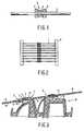
- FIG. 1shows the conductive wire
- FIG. 2shows the wires packed in a tape
- FIG. 3shows schematically a wave soldering process for a substrate with inserted conductive wires.
- the electrically conductive wire 1usually a copper wire, is provided with two solder balls or dots 2 fixedly secured thereon.
- the solder ballsare spaced apart.
- the small space 3 between the ballsare filled with a flux 4 .
- the wirescan be packed in a tape 5 in well known manner (see FIG. 2 ) for use in a feeder of, for example, a component placement machine.
- a component placement machinethe wires are inserted in through-holes 7 of a substrate 6 or printed circuit board in such a manner that the ends 8 of a wire make contact with or are close to a conductive track 9 provided on one of the surfaces 10 of the substrate and the solder balls 2 with flux 4 between them make contact with or are close to a conductive track 11 provided on the opposite surface 12 of the substrate.
- the substrateis transported through, for example, a wave soldering machine 13 , as shown in FIG. 3 .
- the surface 10 of the substratefaces the hot solder 14 .
- the hot soldertouches the ends 8 of the wire 1 , which are then soldered to their respective conductive tracks 9 .
- the heat of the hot solder 14is also transferred through the wire 2 to the solder balls 2 situated at the opposite surface 12 of the substrate.
- the solder ballsmelt and the conductive track surfaces to be wetted by solder are cleaned by means of the flux, so that a reliable connection is obtained.
- a composition of solder with tin, lead and bismuthsuch as Sn43PB43Bi14, the melting temperature is reduced, resulting in a better electrical connection.
Landscapes
- Engineering & Computer Science (AREA)
- Manufacturing & Machinery (AREA)
- Microelectronics & Electronic Packaging (AREA)
- Electric Connection Of Electric Components To Printed Circuits (AREA)
- Connections Effected By Soldering, Adhesion, Or Permanent Deformation (AREA)
- Manufacturing Of Electrical Connectors (AREA)
- Multi-Conductor Connections (AREA)
- Coupling Device And Connection With Printed Circuit (AREA)
Abstract
Description
This is a divisional of divisional application Ser. No. 10/011,741, filed Dec. 11, 2001 now U.S. Pat. No. 6,752,310 which is a divisional of application Ser. No. 08/752,865, filed Nov. 20, 1996 now U.S. Pat. No. 6,410,854. The entire disclosure of the above-referenced prior applications is considered as being part of the disclosure of the accompanying divisional application and is hereby incorporated by reference there in.
The invention relates to an electrically conductive wire having a solder ball thereon for making a circuit connection between electrically conductive members on opposite surfaces of a substrate by means of a soldering process.
For circuit connection across both surfaces of a substrate, a through-hole substrate is known from EP-A-O 126 164. For making the circuit connection an electrically conductive wire having a solder ball thereon is used. The wire is inserted in the through-hole of the substrate. The substrate has electrically conductive members on both surfaces and the conductive members are arranged on the perimeters of the through-hole. The solder ball on the wire is positioned on one of the conductive members. By means of a soldering process, like dipping or flow soldering, one or both ends of the wire are soldered to a conductive member at one surface of the substrate, whereas at the same time heat generated during the soldering process is transferred through the wire to the solder ball at the opposite surface of the substrate in order to melt the solder ball for making a soldering connection between the wire and the conductive member at the opposite surface of the substrate. In this way the circuit connection between the conductive members on both surfaces of the substrate is made.
In practice it has turned out that to make a circuit connection with the use of a single solder ball on it as described hereinbefore, often leads to a bad connection between the conductive members.
Therefore many manufacturers use a separate soldering robot for making such circuit connections. However, this method is rather expensive and results in a limitation in design, logistics, maintenance and process control.
The object of the invention is to provide an electrically conductive wire means for making a reliable circuit connection between electrically conductive members on opposite surfaces of a substrate.
The present invention provides an electrically conductive wire having a solder ball thereon for making a circuit connection between electrically conductive members on opposite surfaces of a substrate, characterized in that the wire comprises two spaced apart solder balls on it and flux in the space between the solder balls.
Using this kind of wires for making circuit connections across both surfaces of a substrate results in a good and reliable connection. The wires are very suitable for use in an automatic soldering process, like reflow or wave soldering. The wire can be inserted in the through-hole of a substrate during the process of placing other components with the same machine. In one of the subsequent operation steps the components are soldered at their required position. At the same time the wires can be soldered in the same soldering process. So, the most important advantage is that the wires can be soldered during existing automatic soldering processes of other components. Preferably the solder balls are composed of tin, lead and bismuth instead of tin and lead only as usually used. The addition of bismuth reduces the melting temperature of the solder.
The present invention will now be described, by way of example, with reference to the accompanying drawings, wherein:
The electrically conductive wire1, usually a copper wire, is provided with two solder balls ordots 2 fixedly secured thereon. The solder balls are spaced apart. Thesmall space 3 between the balls are filled with aflux 4. The wires can be packed in atape 5 in well known manner (seeFIG. 2 ) for use in a feeder of, for example, a component placement machine. In a component placement machine the wires are inserted in through-holes 7 of asubstrate 6 or printed circuit board in such a manner that the ends8 of a wire make contact with or are close to aconductive track 9 provided on one of thesurfaces 10 of the substrate and thesolder balls 2 withflux 4 between them make contact with or are close to aconductive track 11 provided on theopposite surface 12 of the substrate. Usually other components are also placed on the substrate as well. For electrically connecting the wires and components, the substrate is transported through, for example, awave soldering machine 13, as shown in FIG.3. Thesurface 10 of the substrate faces thehot solder 14. The hot solder touches the ends8 of the wire1, which are then soldered to their respectiveconductive tracks 9. The heat of thehot solder 14 is also transferred through thewire 2 to thesolder balls 2 situated at theopposite surface 12 of the substrate. The solder balls melt and the conductive track surfaces to be wetted by solder are cleaned by means of the flux, so that a reliable connection is obtained. By using a composition of solder with tin, lead and bismuth, such as Sn43PB43Bi14, the melting temperature is reduced, resulting in a better electrical connection.
Claims (6)
1. A method of soldering comprising:
disposing first and second balls of solder adjacent one another on a wire;
disposing flux on the wire between and in contact with both of the first and second balls and so as to substantially fill a space between the first and second balls;
disposing the wire on a substrate so that the first and second balls of solder contact a single conductor on the substrate; and
melting the first and second balls of solder and flux and soldering the wire to the conductor.
2. A method as set forth inclaim 1 , wherein the melting is achieved using a wave soldering machine.
3. A method of soldering comprising:
preparing a solderable assembly by:
fixing a first solder ball on a wire;
fixing a second solder ball fixed on the wire with such spacing between the first solder ball and the second solder ball that both of the solder balls can contact a single conductive contact; and
fixing flux on the wire and forming a continuous layer substantially filling the space between the first and second solder balls.
4. A method as set forth inclaim 3 , further comprising:
deploying the solderable assembly so that the first and second solder balls are disposed on the single contact; and
heating the solderable assembly so that the solder balls and flux flow and make a single reliable connection.
5. A method as set forth inclaim 4 , wherein heating the solderable assembly comprises heating the wire and conducting heat through the wire to the flux and the first and second balls of solder.
6. A method of soldering comprising:
preparing a solderable assembly by:
fixing a first solder ball on a wire;
fixing a second solder ball fixed on the wire with such spacing between the first solder ball and the second solder ball that both of the solder balls can contact a single conductive contact; and
fixing flux on the wire and forming a continuous layer substantially filling the space between the first and second solder balls;
deploying the solderable assembly so that the first and second solder balls are disposed on the single contact;
heating the solderable assembly so that the solder balls and flux flow and make a single reliable connection;
disposing a portion of the wire through an aperture in a substrate heating wire which has passed through the aperture.
Priority Applications (2)
| Application Number | Priority Date | Filing Date | Title |
|---|---|---|---|
| US10/817,824US6902097B2 (en) | 1995-11-20 | 2004-04-06 | Electrically conductive wire |
| US11/134,693US20050224932A1 (en) | 1995-11-20 | 2005-05-20 | Electrically conductive wire |
Applications Claiming Priority (5)
| Application Number | Priority Date | Filing Date | Title |
|---|---|---|---|
| EP95203166 | 1995-11-20 | ||
| EP95203166.4 | 1995-11-20 | ||
| US08/752,865US6410854B1 (en) | 1995-11-20 | 1996-11-20 | Wire and solder arrangement of ease of wave soldering |
| US10/011,741US6752310B2 (en) | 1995-11-20 | 2001-12-11 | Electrically conductive wire |
| US10/817,824US6902097B2 (en) | 1995-11-20 | 2004-04-06 | Electrically conductive wire |
Related Parent Applications (1)
| Application Number | Title | Priority Date | Filing Date |
|---|---|---|---|
| US10/011,741DivisionUS6752310B2 (en) | 1995-11-20 | 2001-12-11 | Electrically conductive wire |
Related Child Applications (1)
| Application Number | Title | Priority Date | Filing Date |
|---|---|---|---|
| US11/134,693DivisionUS20050224932A1 (en) | 1995-11-20 | 2005-05-20 | Electrically conductive wire |
Publications (2)
| Publication Number | Publication Date |
|---|---|
| US20040188498A1 US20040188498A1 (en) | 2004-09-30 |
| US6902097B2true US6902097B2 (en) | 2005-06-07 |
Family
ID=8220841
Family Applications (4)
| Application Number | Title | Priority Date | Filing Date |
|---|---|---|---|
| US08/752,865Expired - Fee RelatedUS6410854B1 (en) | 1995-11-20 | 1996-11-20 | Wire and solder arrangement of ease of wave soldering |
| US10/011,741Expired - Fee RelatedUS6752310B2 (en) | 1995-11-20 | 2001-12-11 | Electrically conductive wire |
| US10/817,824Expired - Fee RelatedUS6902097B2 (en) | 1995-11-20 | 2004-04-06 | Electrically conductive wire |
| US11/134,693AbandonedUS20050224932A1 (en) | 1995-11-20 | 2005-05-20 | Electrically conductive wire |
Family Applications Before (2)
| Application Number | Title | Priority Date | Filing Date |
|---|---|---|---|
| US08/752,865Expired - Fee RelatedUS6410854B1 (en) | 1995-11-20 | 1996-11-20 | Wire and solder arrangement of ease of wave soldering |
| US10/011,741Expired - Fee RelatedUS6752310B2 (en) | 1995-11-20 | 2001-12-11 | Electrically conductive wire |
Family Applications After (1)
| Application Number | Title | Priority Date | Filing Date |
|---|---|---|---|
| US11/134,693AbandonedUS20050224932A1 (en) | 1995-11-20 | 2005-05-20 | Electrically conductive wire |
Country Status (5)
| Country | Link |
|---|---|
| US (4) | US6410854B1 (en) |
| EP (1) | EP0804817A1 (en) |
| JP (1) | JPH10513308A (en) |
| KR (1) | KR100404275B1 (en) |
| WO (1) | WO1997019491A1 (en) |
Cited By (1)
| Publication number | Priority date | Publication date | Assignee | Title |
|---|---|---|---|---|
| US20050224932A1 (en)* | 1995-11-20 | 2005-10-13 | Vanhoutte Eddy W | Electrically conductive wire |
Families Citing this family (19)
| Publication number | Priority date | Publication date | Assignee | Title |
|---|---|---|---|---|
| US6631842B1 (en) | 2000-06-07 | 2003-10-14 | Metrologic Instruments, Inc. | Method of and system for producing images of objects using planar laser illumination beams and image detection arrays |
| US6587446B2 (en) | 1999-02-11 | 2003-07-01 | Qualcomm Incorporated | Handoff in a wireless communication system |
| DE19928320A1 (en)* | 1999-06-16 | 2001-01-04 | Siemens Ag | Electrically conductive connection between an end electrode and a connecting wire |
| WO2001085997A1 (en)* | 2000-05-08 | 2001-11-15 | Qtl Biosystems Llc | Improvements to the fluorescent polymer-qtl approach to biosensing |
| US7128266B2 (en) | 2003-11-13 | 2006-10-31 | Metrologic Instruments. Inc. | Hand-supportable digital imaging-based bar code symbol reader supporting narrow-area and wide-area modes of illumination and image capture |
| US7540424B2 (en) | 2000-11-24 | 2009-06-02 | Metrologic Instruments, Inc. | Compact bar code symbol reading system employing a complex of coplanar illumination and imaging stations for omni-directional imaging of objects within a 3D imaging volume |
| US7490774B2 (en) | 2003-11-13 | 2009-02-17 | Metrologic Instruments, Inc. | Hand-supportable imaging based bar code symbol reader employing automatic light exposure measurement and illumination control subsystem integrated therein |
| US7464877B2 (en) | 2003-11-13 | 2008-12-16 | Metrologic Instruments, Inc. | Digital imaging-based bar code symbol reading system employing image cropping pattern generator and automatic cropped image processor |
| US8042740B2 (en) | 2000-11-24 | 2011-10-25 | Metrologic Instruments, Inc. | Method of reading bar code symbols on objects at a point-of-sale station by passing said objects through a complex of stationary coplanar illumination and imaging planes projected into a 3D imaging volume |
| US7708205B2 (en) | 2003-11-13 | 2010-05-04 | Metrologic Instruments, Inc. | Digital image capture and processing system employing multi-layer software-based system architecture permitting modification and/or extension of system features and functions by way of third party code plug-ins |
| WO2004049982A2 (en)* | 2002-12-02 | 2004-06-17 | Gi Dynamics, Inc. | Bariatric sleeve |
| US7608114B2 (en)* | 2002-12-02 | 2009-10-27 | Gi Dynamics, Inc. | Bariatric sleeve |
| WO2004087233A2 (en)* | 2003-03-28 | 2004-10-14 | Gi Dynamics, Inc. | Sleeve for delayed introduction of enzymes into the intestine |
| US7841533B2 (en)* | 2003-11-13 | 2010-11-30 | Metrologic Instruments, Inc. | Method of capturing and processing digital images of an object within the field of view (FOV) of a hand-supportable digitial image capture and processing system |
| AU2004305450B2 (en) | 2003-12-09 | 2009-01-08 | Gi Dynamics, Inc. | Intestinal sleeve |
| EP1799145B1 (en)* | 2004-09-17 | 2016-12-21 | GI Dynamics, Inc. | Gastrointestinal anchor |
| US7976488B2 (en)* | 2005-06-08 | 2011-07-12 | Gi Dynamics, Inc. | Gastrointestinal anchor compliance |
| US10655363B2 (en)* | 2014-09-26 | 2020-05-19 | Assa Abloy Inc. | Integrated lock body system for securing access points |
| DE102023129071A1 (en)* | 2023-10-23 | 2025-04-24 | Endress+Hauser SE+Co. KG | Solder preform for receiving a jumper, use of the solder preform, and system and method for connecting two printed circuit boards by means of a jumper |
Citations (18)
| Publication number | Priority date | Publication date | Assignee | Title |
|---|---|---|---|---|
| US2258750A (en) | 1940-12-12 | 1941-10-14 | Eichwald Benjamin | Terminal block |
| FR1387555A (en) | 1964-03-05 | 1965-01-29 | Philips Nv | Assembly of two electrically conductive bodies |
| US3541225A (en) | 1968-12-20 | 1970-11-17 | Gen Electric | Electrical conductor with improved solder characteristics |
| US3616981A (en)* | 1969-08-08 | 1971-11-02 | Erie Technological Prod Inc | Lead and solder preform assembly and method of making the same |
| US3693052A (en) | 1971-04-15 | 1972-09-19 | Warwick Electronics Inc | Electrical component mounting |
| US3770874A (en) | 1970-09-08 | 1973-11-06 | Siemens Ag | Contact members for soldering electrical components |
| US3889364A (en) | 1972-06-02 | 1975-06-17 | Siemens Ag | Method of making soldered electrical connections |
| US3925596A (en) | 1972-06-12 | 1975-12-09 | Raychem Corp | Heat recoverable connectors |
| CA1052475A (en) | 1975-03-03 | 1979-04-10 | Hiroshi Fukuhara | Double faced printed circuit board interconnection |
| EP0126164A1 (en) | 1982-11-27 | 1984-11-28 | Matsushita Electric Industrial Co., Ltd. | Method of connecting double-sided circuits |
| US4809901A (en)* | 1981-10-05 | 1989-03-07 | Raychem Corporation | Soldering methods and devices |
| US5093545A (en)* | 1988-09-09 | 1992-03-03 | Metcal, Inc. | Method, system and composition for soldering by induction heating |
| JPH04127547A (en) | 1990-09-19 | 1992-04-28 | Nec Corp | Lsi mounting structure |
| US5110034A (en) | 1990-08-30 | 1992-05-05 | Quantum Magnetics, Inc. | Superconducting bonds for thin film devices |
| US5298877A (en) | 1993-02-19 | 1994-03-29 | Cooper Industries, Inc. | Fuse link and dual element fuse |
| US5328087A (en) | 1993-03-29 | 1994-07-12 | Microelectronics And Computer Technology Corporation | Thermally and electrically conductive adhesive material and method of bonding with same |
| US5427865A (en) | 1994-05-02 | 1995-06-27 | Motorola, Inc. | Multiple alloy solder preform |
| US6410854B1 (en)* | 1995-11-20 | 2002-06-25 | Koninklijke Philips Electronics N.V. | Wire and solder arrangement of ease of wave soldering |
Family Cites Families (4)
| Publication number | Priority date | Publication date | Assignee | Title |
|---|---|---|---|---|
| US3889264A (en)* | 1973-05-21 | 1975-06-10 | Nasa | Vehicle locating system utilizing AM broadcasting station carriers |
| US4189083A (en)* | 1978-06-15 | 1980-02-19 | Motorola, Inc. | Low temperature and low cost assembly process for nonlinear resistors |
| JP2756184B2 (en)* | 1990-11-27 | 1998-05-25 | 株式会社日立製作所 | Surface mounting structure of electronic components |
| WO1996010279A1 (en)* | 1994-09-29 | 1996-04-04 | North American Specialties Corporation | Solder-bearing lead and method of producing and using same |
- 1996
- 1996-11-13JPJP9519537Apatent/JPH10513308A/ennot_activeCeased
- 1996-11-13EPEP96935237Apatent/EP0804817A1/ennot_activeWithdrawn
- 1996-11-13WOPCT/IB1996/001203patent/WO1997019491A1/enactiveIP Right Grant
- 1996-11-13KRKR1019970704831Apatent/KR100404275B1/ennot_activeExpired - Fee Related
- 1996-11-20USUS08/752,865patent/US6410854B1/ennot_activeExpired - Fee Related
- 2001
- 2001-12-11USUS10/011,741patent/US6752310B2/ennot_activeExpired - Fee Related
- 2004
- 2004-04-06USUS10/817,824patent/US6902097B2/ennot_activeExpired - Fee Related
- 2005
- 2005-05-20USUS11/134,693patent/US20050224932A1/ennot_activeAbandoned
Patent Citations (20)
| Publication number | Priority date | Publication date | Assignee | Title |
|---|---|---|---|---|
| US2258750A (en) | 1940-12-12 | 1941-10-14 | Eichwald Benjamin | Terminal block |
| FR1387555A (en) | 1964-03-05 | 1965-01-29 | Philips Nv | Assembly of two electrically conductive bodies |
| US3541225A (en) | 1968-12-20 | 1970-11-17 | Gen Electric | Electrical conductor with improved solder characteristics |
| US3616981A (en)* | 1969-08-08 | 1971-11-02 | Erie Technological Prod Inc | Lead and solder preform assembly and method of making the same |
| US3770874A (en) | 1970-09-08 | 1973-11-06 | Siemens Ag | Contact members for soldering electrical components |
| US3693052A (en) | 1971-04-15 | 1972-09-19 | Warwick Electronics Inc | Electrical component mounting |
| US3889364A (en) | 1972-06-02 | 1975-06-17 | Siemens Ag | Method of making soldered electrical connections |
| US3925596A (en) | 1972-06-12 | 1975-12-09 | Raychem Corp | Heat recoverable connectors |
| CA1052475A (en) | 1975-03-03 | 1979-04-10 | Hiroshi Fukuhara | Double faced printed circuit board interconnection |
| US4809901A (en)* | 1981-10-05 | 1989-03-07 | Raychem Corporation | Soldering methods and devices |
| US4592137A (en) | 1982-11-27 | 1986-06-03 | Matsushita Electric Industrial Co., Ltd. | Method of circuit connection across both surfaces of substrate |
| EP0126164A1 (en) | 1982-11-27 | 1984-11-28 | Matsushita Electric Industrial Co., Ltd. | Method of connecting double-sided circuits |
| US5093545A (en)* | 1988-09-09 | 1992-03-03 | Metcal, Inc. | Method, system and composition for soldering by induction heating |
| US5110034A (en) | 1990-08-30 | 1992-05-05 | Quantum Magnetics, Inc. | Superconducting bonds for thin film devices |
| JPH04127547A (en) | 1990-09-19 | 1992-04-28 | Nec Corp | Lsi mounting structure |
| US5298877A (en) | 1993-02-19 | 1994-03-29 | Cooper Industries, Inc. | Fuse link and dual element fuse |
| US5328087A (en) | 1993-03-29 | 1994-07-12 | Microelectronics And Computer Technology Corporation | Thermally and electrically conductive adhesive material and method of bonding with same |
| US5427865A (en) | 1994-05-02 | 1995-06-27 | Motorola, Inc. | Multiple alloy solder preform |
| US6410854B1 (en)* | 1995-11-20 | 2002-06-25 | Koninklijke Philips Electronics N.V. | Wire and solder arrangement of ease of wave soldering |
| US6752310B2 (en)* | 1995-11-20 | 2004-06-22 | Koninklijke Philips Electronics N.V. | Electrically conductive wire |
Cited By (1)
| Publication number | Priority date | Publication date | Assignee | Title |
|---|---|---|---|---|
| US20050224932A1 (en)* | 1995-11-20 | 2005-10-13 | Vanhoutte Eddy W | Electrically conductive wire |
Also Published As
| Publication number | Publication date |
|---|---|
| US20020040804A1 (en) | 2002-04-11 |
| JPH10513308A (en) | 1998-12-15 |
| KR100404275B1 (en) | 2004-03-12 |
| US6752310B2 (en) | 2004-06-22 |
| EP0804817A1 (en) | 1997-11-05 |
| US6410854B1 (en) | 2002-06-25 |
| KR19980701441A (en) | 1998-05-15 |
| US20040188498A1 (en) | 2004-09-30 |
| WO1997019491A1 (en) | 1997-05-29 |
| US20050224932A1 (en) | 2005-10-13 |
Similar Documents
| Publication | Publication Date | Title |
|---|---|---|
| US6902097B2 (en) | Electrically conductive wire | |
| US5172852A (en) | Soldering method | |
| US5477419A (en) | Method and apparatus for electrically connecting an electronic part to a circuit board | |
| US5783865A (en) | Wiring substrate and semiconductor device | |
| EP0473929B1 (en) | Method of forming a thin film electronic device | |
| US5115964A (en) | Method for bonding thin film electronic device | |
| GB2202682A (en) | Connection leads for surface mounted components | |
| US5438749A (en) | Method of making a flex circuit interconnect for a microprocessor emulator and a method of testing | |
| US20020061687A1 (en) | Solder bearing grid array | |
| US6296174B1 (en) | Method and circuit board for assembling electronic devices | |
| EP0568087A2 (en) | Reflow mounting of electronic component on mounting board | |
| JP2001217027A (en) | Pillar grid disposed connector | |
| JP3410199B2 (en) | Device for preventing bridging of connection member, semiconductor integrated circuit having the same, and mounting substrate | |
| JPS61102089A (en) | Mount structure of flat package ic | |
| US20030079911A1 (en) | Discrete solder ball contact and circuit board assembly utilizing same | |
| GB2132538A (en) | Method of soldering a conductive element to a conductor pad | |
| EP0876691B1 (en) | Solder element | |
| JPS6129159B2 (en) | ||
| JPS60182189A (en) | Soldering method and electric circuit device | |
| JPH03101191A (en) | Method of filling via-hole | |
| EP0676913A1 (en) | Surface-mount component soldering | |
| JPH05283587A (en) | Soldering method of multiple-lead element | |
| JPS6151945A (en) | Semiconductor device | |
| JPH0767010B2 (en) | Double-sided printed circuit board component mounting method | |
| JPH07307559A (en) | Soldering structure and method of electronic component |
Legal Events
| Date | Code | Title | Description |
|---|---|---|---|
| REMI | Maintenance fee reminder mailed | ||
| LAPS | Lapse for failure to pay maintenance fees | ||
| STCH | Information on status: patent discontinuation | Free format text:PATENT EXPIRED DUE TO NONPAYMENT OF MAINTENANCE FEES UNDER 37 CFR 1.362 | |
| FP | Expired due to failure to pay maintenance fee | Effective date:20090607 |