US6900869B1 - Multi-domain liquid crystal display device with particular dielectric structures - Google Patents
Multi-domain liquid crystal display device with particular dielectric structuresDownload PDFInfo
- Publication number
- US6900869B1 US6900869B1US09/448,276US44827699AUS6900869B1US 6900869 B1US6900869 B1US 6900869B1US 44827699 AUS44827699 AUS 44827699AUS 6900869 B1US6900869 B1US 6900869B1
- Authority
- US
- United States
- Prior art keywords
- liquid crystal
- substrate
- layer
- crystal display
- display device
- Prior art date
- Legal status (The legal status is an assumption and is not a legal conclusion. Google has not performed a legal analysis and makes no representation as to the accuracy of the status listed.)
- Expired - Lifetime
Links
Images


Classifications
- G—PHYSICS
- G02—OPTICS
- G02F—OPTICAL DEVICES OR ARRANGEMENTS FOR THE CONTROL OF LIGHT BY MODIFICATION OF THE OPTICAL PROPERTIES OF THE MEDIA OF THE ELEMENTS INVOLVED THEREIN; NON-LINEAR OPTICS; FREQUENCY-CHANGING OF LIGHT; OPTICAL LOGIC ELEMENTS; OPTICAL ANALOGUE/DIGITAL CONVERTERS
- G02F1/00—Devices or arrangements for the control of the intensity, colour, phase, polarisation or direction of light arriving from an independent light source, e.g. switching, gating or modulating; Non-linear optics
- G02F1/01—Devices or arrangements for the control of the intensity, colour, phase, polarisation or direction of light arriving from an independent light source, e.g. switching, gating or modulating; Non-linear optics for the control of the intensity, phase, polarisation or colour
- G02F1/13—Devices or arrangements for the control of the intensity, colour, phase, polarisation or direction of light arriving from an independent light source, e.g. switching, gating or modulating; Non-linear optics for the control of the intensity, phase, polarisation or colour based on liquid crystals, e.g. single liquid crystal display cells
- G02F1/133—Constructional arrangements; Operation of liquid crystal cells; Circuit arrangements
- G02F1/1333—Constructional arrangements; Manufacturing methods
- G02F1/1337—Surface-induced orientation of the liquid crystal molecules, e.g. by alignment layers
- G02F1/133707—Structures for producing distorted electric fields, e.g. bumps, protrusions, recesses, slits in pixel electrodes
- G—PHYSICS
- G02—OPTICS
- G02F—OPTICAL DEVICES OR ARRANGEMENTS FOR THE CONTROL OF LIGHT BY MODIFICATION OF THE OPTICAL PROPERTIES OF THE MEDIA OF THE ELEMENTS INVOLVED THEREIN; NON-LINEAR OPTICS; FREQUENCY-CHANGING OF LIGHT; OPTICAL LOGIC ELEMENTS; OPTICAL ANALOGUE/DIGITAL CONVERTERS
- G02F1/00—Devices or arrangements for the control of the intensity, colour, phase, polarisation or direction of light arriving from an independent light source, e.g. switching, gating or modulating; Non-linear optics
- G02F1/01—Devices or arrangements for the control of the intensity, colour, phase, polarisation or direction of light arriving from an independent light source, e.g. switching, gating or modulating; Non-linear optics for the control of the intensity, phase, polarisation or colour
- G02F1/13—Devices or arrangements for the control of the intensity, colour, phase, polarisation or direction of light arriving from an independent light source, e.g. switching, gating or modulating; Non-linear optics for the control of the intensity, phase, polarisation or colour based on liquid crystals, e.g. single liquid crystal display cells
- G02F1/133—Constructional arrangements; Operation of liquid crystal cells; Circuit arrangements
- G02F1/1333—Constructional arrangements; Manufacturing methods
- G02F1/1335—Structural association of cells with optical devices, e.g. polarisers or reflectors
- G02F1/133509—Filters, e.g. light shielding masks
- G02F1/133512—Light shielding layers, e.g. black matrix
- G—PHYSICS
- G02—OPTICS
- G02F—OPTICAL DEVICES OR ARRANGEMENTS FOR THE CONTROL OF LIGHT BY MODIFICATION OF THE OPTICAL PROPERTIES OF THE MEDIA OF THE ELEMENTS INVOLVED THEREIN; NON-LINEAR OPTICS; FREQUENCY-CHANGING OF LIGHT; OPTICAL LOGIC ELEMENTS; OPTICAL ANALOGUE/DIGITAL CONVERTERS
- G02F1/00—Devices or arrangements for the control of the intensity, colour, phase, polarisation or direction of light arriving from an independent light source, e.g. switching, gating or modulating; Non-linear optics
- G02F1/01—Devices or arrangements for the control of the intensity, colour, phase, polarisation or direction of light arriving from an independent light source, e.g. switching, gating or modulating; Non-linear optics for the control of the intensity, phase, polarisation or colour
- G02F1/13—Devices or arrangements for the control of the intensity, colour, phase, polarisation or direction of light arriving from an independent light source, e.g. switching, gating or modulating; Non-linear optics for the control of the intensity, phase, polarisation or colour based on liquid crystals, e.g. single liquid crystal display cells
- G02F1/133—Constructional arrangements; Operation of liquid crystal cells; Circuit arrangements
- G02F1/1333—Constructional arrangements; Manufacturing methods
- G02F1/1337—Surface-induced orientation of the liquid crystal molecules, e.g. by alignment layers
- G02F1/133753—Surface-induced orientation of the liquid crystal molecules, e.g. by alignment layers with different alignment orientations or pretilt angles on a same surface, e.g. for grey scale or improved viewing angle
- G—PHYSICS
- G02—OPTICS
- G02F—OPTICAL DEVICES OR ARRANGEMENTS FOR THE CONTROL OF LIGHT BY MODIFICATION OF THE OPTICAL PROPERTIES OF THE MEDIA OF THE ELEMENTS INVOLVED THEREIN; NON-LINEAR OPTICS; FREQUENCY-CHANGING OF LIGHT; OPTICAL LOGIC ELEMENTS; OPTICAL ANALOGUE/DIGITAL CONVERTERS
- G02F1/00—Devices or arrangements for the control of the intensity, colour, phase, polarisation or direction of light arriving from an independent light source, e.g. switching, gating or modulating; Non-linear optics
- G02F1/01—Devices or arrangements for the control of the intensity, colour, phase, polarisation or direction of light arriving from an independent light source, e.g. switching, gating or modulating; Non-linear optics for the control of the intensity, phase, polarisation or colour
- G02F1/13—Devices or arrangements for the control of the intensity, colour, phase, polarisation or direction of light arriving from an independent light source, e.g. switching, gating or modulating; Non-linear optics for the control of the intensity, phase, polarisation or colour based on liquid crystals, e.g. single liquid crystal display cells
- G02F1/137—Devices or arrangements for the control of the intensity, colour, phase, polarisation or direction of light arriving from an independent light source, e.g. switching, gating or modulating; Non-linear optics for the control of the intensity, phase, polarisation or colour based on liquid crystals, e.g. single liquid crystal display cells characterised by the electro-optical or magneto-optical effect, e.g. field-induced phase transition, orientation effect, guest-host interaction or dynamic scattering
- G02F1/139—Devices or arrangements for the control of the intensity, colour, phase, polarisation or direction of light arriving from an independent light source, e.g. switching, gating or modulating; Non-linear optics for the control of the intensity, phase, polarisation or colour based on liquid crystals, e.g. single liquid crystal display cells characterised by the electro-optical or magneto-optical effect, e.g. field-induced phase transition, orientation effect, guest-host interaction or dynamic scattering based on orientation effects in which the liquid crystal remains transparent
- G02F1/1393—Devices or arrangements for the control of the intensity, colour, phase, polarisation or direction of light arriving from an independent light source, e.g. switching, gating or modulating; Non-linear optics for the control of the intensity, phase, polarisation or colour based on liquid crystals, e.g. single liquid crystal display cells characterised by the electro-optical or magneto-optical effect, e.g. field-induced phase transition, orientation effect, guest-host interaction or dynamic scattering based on orientation effects in which the liquid crystal remains transparent the birefringence of the liquid crystal being electrically controlled, e.g. ECB-, DAP-, HAN-, PI-LC cells
Definitions
- the present inventionrelates to a liquid crystal display device (LCD), and more particularly, to a liquid crystal display device having a dielectric frame.
- LCDliquid crystal display device
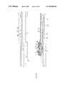
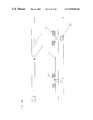
- FIG. 1is sectional view of pixel unit of the conventional LCDs.
- a plurality of gate bus lines arranged in a first direction on a first substrate and a plurality of data bus lines arranged in a second direction on the first substratedivide the first substrate into a plurality of pixel regions.
- a thin film transistorapplies image signal delivered from the data bus line to a pixel electrode 13 on a passivation layer 37 .
- the TFTis formed on each pixel region and comprises a gate electrode, a gate insulator, a semiconductor layer, a source electrode, and a drain electrode, etc.
- Side electrode 15is formed surrounding the pixel electrode 13 on the gate insulator, thereon passivation layer 37 is formed over the whole first substrate, and a part of pixel electrode 13 overlaps side electrode 15 .
- pixel electrode 13is formed on the gate insulator, and passivation layer 37 is formed over the whole first substrate.
- a common electrode 17is formed and together with pixel electrode 13 applies electric field to a liquid crystal layer.
- Side electrode 21 and open area (slit) 27distort the electric field applied to the liquid crystal layer. Then, in a unit pixel liquid crystal molecules are driven variously. This means that when voltage is applied to the LCD, dielectric energy due to the distorted electric field arranges the liquid crystal directors in needed or desired positions.
- the time needed to stabilize the liquid crystal directorsincreases.
- the response timecan be over 100 msec.
- disclinationoccurs from the area where the liquid crystal directors are parallel with a transmittance axis of the polarizer, which results in a decrease in brightness.
- the liquid crystal texturehas an irregular structure.
- the present inventionis directed to an LCD that substantially obviates one or more problems due to limitations and disadvantages of the related art.
- An object of the present inventionis to provide a multi-domain LCD having high response time characteristics and high brightness by stable arrangement of liquid crystal molecules.
- a multi-domain liquid crystal display devicecomprises first and second substrates facing each other, a liquid crystal layer between the first and second substrates, a plurality of gate bus lines arranged in a first direction on the first substrate and a plurality of data bus lines arranged in a second direction on the first substrate to define a pixel region, a pixel electrode in the pixel region, a dielectric frame in a region other than a region where the pixel electrode is formed, the dielectric frame distorting electric field applied to the liquid crystal layer, a common electrode on the second substrate, and an alignment layer on at least one substrate between the first and second substrates.
- the dielectric framemaintains uniformly gap between the first and second substrates, or shields light leakage from a region other than the pixel region.
- FIG. 1is a sectional view of the liquid crystal display device in the related art
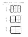
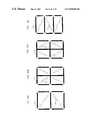
- FIGS. 2A , 2 B, 2 C, and 2 Dare sectional views of the multi-domain liquid crystal display devices according to the first embodiment of the present invention.
- FIGS. 3A , 3 B, and 3 Care sectional views of the multi-domain liquid crystal display devices according to the second embodiment of the present invention.
- FIGS. 4A , 4 B, 4 C, and 4 Dare plan views showing various electric field inducing window and dielectric frame of the multi-domain liquid crystal display devices according to an embodiment of the present invention
- FIGS. 5A , 5 B, 5 C, and 5 Dare plan views showing various electric field inducing window and dielectric frame of the multi-domain liquid crystal display devices according to an embodiment of the present invention
- FIGS. 6A , 6 B, 6 C, and 6 Dare plan views showing various electric field inducing window and dielectric frame of the multi-domain liquid crystal display devices according to an embodiment of the present invention.
- FIGS. 7A , 7 B, 7 C, and 7 Dare plan views showing various electric field inducing window and dielectric frame of the multi-domain liquid crystal display devices according to an embodiment of the present invention.
- FIGS. 8A , 8 B, 8 C, 8 D, 8 E, and 8 Fare plan views showing various electric field inducing window and dielectric frame of the multi-domain liquid crystal display devices according to an embodiment of the present invention.
- FIGS. 9A , 9 B, and 9 Care plan views showing various electric field inducing window and dielectric frame of the multi-domain liquid crystal display devices according to an embodiment of the present invention.
- FIGS. 10A , 10 B, and 10 Care plan views showing various electric field inducing window and dielectric frame of the multi-domain liquid crystal display devices according to an embodiment of the present invention.
- FIGS. 11A , 11 B, 11 C, 11 D, 11 E, and 11 Fare plan views showing various electric field inducing window and dielectric frame of the multi-domain liquid crystal display devices according to an embodiment of the present invention.
- FIGS. 12A , 12 B, 12 C, 12 D, 12 E and 12 Fare plan views showing various electric field inducing window and dielectric frame of the multi-domain liquid crystal display devices according to an embodiment of the present invention
- FIGS. 13A , 13 B, 13 C, 13 D, 13 E, 13 F, 13 G and 13 Hare plan views showing various electric field inducing window and dielectric frame of the multi-domain liquid crystal display devices according to an embodiment of the present invention
- FIGS. 14A and 14Bare plan views showing various electric field inducing window and dielectric frame of the multi-domain liquid crystal display devices according to an embodiment of the present invention.
- FIGS. 15A and 15Bare views showing various electric field inducing window and dielectric frame of the multi-domain liquid crystal display devices according to another embodiment of the present invention.
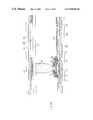
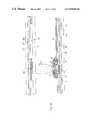
- FIGS. 2A , 2 B, 2 C, and 2 Dare sectional views of the multi-domain liquid crystal display devices according to the first embodiment of the present invention and FIGS. 3A , 3 B, and 3 C are sectional views of the multi-domain liquid crystal display devices according to the second embodiment of the present invention.
- the present inventioncomprises first and second substrates 31 , 33 , a plurality of gate bus lines 1 arranged in a first direction on a first substrate and a plurality of data bus lines 3 arranged in a second direction on the first substrate, a TFT, a passivation layer 37 , and a pixel electrode 13 .
- a light shielding layer 25is formed to shield the light leaked from gate and data bus lines 1 , 3 , and the TFT, a color filter layer 23 is formed on the light shielding layer, a common electrode 17 is formed on the color filter layer, a dielectric frame in a region other than the pixel region, and a liquid crystal layer is formed between the first and second substrates.
- Data bus lines 3 and gate bus lines 1divide the first substrate 31 into a plurality of pixel regions.
- the TFTis formed on each pixel region and comprises a gate electrode 11 , a gate insulator 35 , a semiconductor layer 5 , an ohmic contact layer 6 , and source/drain electrodes 7 , 9 .
- Passivation layer 37is formed on the whole first substrate 31 .
- Pixel electrode 13is coupled to the drain electrode 9 .
- a TFTis formed comprising gate electrode 11 , gate insulator 35 , semiconductor layer 5 , ohmic contact layer 6 and source/drain electrodes 7 , 9 .
- a plurality of gate bus lines 1 and a plurality of data bus lines 3are formed to divide the first substrate 31 into a plurality of pixel regions.
- Gate electrode 11 and gate bus line 1are formed by sputtering and patterning a metal such as Al, Mo, Cr, Ta, Al alloy, etc. Alternatively, it is possible to form the gate electrode and gate bus line as a double layer, the double layer is formed from different materials.
- the gate insulator 35is formed by depositing SiN X , SiO X , or BCB (BenzoCycloButene), acrylic resin using PECVD thereon.
- Semiconductor layer 5 and the ohmic contact layer 6are formed by depositing with PECVD(Plasma Enhancement Chemical Vapor Deposition) and patterning amorphous silicon (a-Si) and doped amorphous silicon (n + a-Si), respectively.
- PECVDPullasma Enhancement Chemical Vapor Deposition
- gate insulator 35 , amorphous silicon (a-Si), and doped amorphous silicon (n + a-Si)can be formed by PECVD and patterned.
- Data bus line 3 and source/drain electrodes 7 , 9are formed by sputtering and patterning a metal such as Al, Mo, Cr, Ta, Al alloy, etc.
- a metalsuch as Al, Mo, Cr, Ta, Al alloy, etc.
- a storage electrode(not shown in the figures) is formed to overlap gate bus line 1 , the storage electrode makes a storage capacitor with gate bus line 1 .
- passivation layer 37is formed with BCB (BenzoCycloButene), acrylic resin, polyimide based material, SiN X or SiO X on the whole first substrate.
- Pixel electrode 13is formed by sputtering and patterning a metal such as ITO(indium tin oxide).
- a contact hole 39is formed to connect the pixel electrode 13 to the drain 9 and storage electrodes by opening and patterning a part of the passivation layer 37 on drain electrode 9 .
- a light shielding layer 25is formed to shield any light leakage from gate and data bus lines 1 , 3 , and the TFT.
- a color filter layer 23is formed R, G, B (red, green, blue) elements to alternate on the light shielding layer 25 .
- a common electrode 17is formed with ITO on the color filter layer 23 , and a liquid crystal layer is formed by injecting liquid crystal between the first and second substrates.
- the liquid crystal layermay include liquid crystal molecules having positive or negative dielectric anisotropy. Also, the liquid crystal layer may include chirals dopants.
- a dielectric frame 53is formed by depositing photosensitive material in a region other than a region where the pixel electrode 13 is formed and patterning in various shapes using photolithography.
- the dielectric frame 53includes material of which dielectric constant is same or smaller than that of the liquid crystal, and the dielectric constant thereof is preferably below 3, for example, photoacrylate or BCB (BenzoCycloButene).
- the dielectric framecould include mixture of polyimide and carbon black or mixture of acrylic resin and carbon black. And then, the dielectric frame shields light leakage from an area except the pixel region and distorts the electric field applied to the liquid crystal layer.
- the dielectric constant of the liquid crystal layeris about 4, preferably the dielectric constant of the dielectric frame is below 3.5.
- the dielectric frameis also used as a spacer to maintain uniformly gap between the first and second substrates.
- the dielectric frame 53is formed on at least one substrate between the first and second substrates.
- an electric field inducing window 51is formed on at least one substrate between the first and second substrates.
- the electric field inducing window 51is formed by patterning hole or slit in the common electrode 17 or pixel electrode 13 .
- a compensation film 29is formed with polymer.
- the compensation filmis a negative uniaxial film, which has one optical axis, and compensates the phase difference of the direction according to viewing-angle. Hence, it is possible to compensate effectively the right-left viewing-angle by widening the area without gray inversion, increasing contrast ratio in an inclined direction, and forming one pixel to multi-domain.
- the compensation filmwhich has two optical axes and wider viewing-angle characteristics as compared with the negative uniaxial film.
- the compensation filmcould be formed on both substrates or on one of them.
- the compensation film and polarizerare preferably composed as one.
- the aperture ratiois enhanced by an optimum structure design of a “n-line” thin film transistor (U.S. Pat. No. 5,694,185) so as to reduce power consumption, increase luminance, and lower reflection, thus improving contrast ratio.
- Aperture ratiois increased by forming the TFT above the gate line and providing a “n-line” TFT.
- the parasitic capacitor, occurring between the gate bus line and the drain electrode,can be reduced when a TFT having the same channel length as the symmetrical TFT structure is manufactured due to effect of channel length extension.
- the multi-domain LCD of the present inventionhas a dielectric frame 53 on the pixel electrode and/or common electrode, or an electric field inducing window 51 like a hole or slit in the pixel electrode, passivation layer, gate insulator, color filter layer, and/or common electrode by patterning, thereby electric field distortion effect and multi-domain are obtained.
- the multi-domainis obtained by dividing each pixel into four domains such as in a “+”, “x”, or “double Y” shape, or dividing each pixel horizontally, vertically, and/or diagonally, and differently alignment-treating or forming alignment directions on each domain and on each substrate.
- FIGS. 4 , 5 , 6 , 7 , 8 , 9 , 10 , 11 , 12 , 13 , 14 and 15are plan views showing various electric field inducing window and dielectric frame of the multi-domain liquid crystal display devices according to embodiments of the present invention.
- the solid lined-arrowrepresents an alignment direction of the second substrate
- the dotted lined-arrowrepresents an alignment direction of the first substrate.
- the dielectric frame 53 and at least one electric field inducing window 51are patterned in various shapes, which obtains multi-domain effect.
- the electric field inducing windowmay be a slit or hole. Furthermore, neighboring two pixels and two alignment directions are associated, which obtains multi-domain effect.
- an alignment layer(not shown in the figure) is formed over the whole first and/or second substrates.
- the alignment layerincludes a material such as polyamide or polyimide based materials, PVA (polyvinylalcohol), polyamic acid or SiO 2 .
- the alignment layerwith a photosensitive material such as PVCN (polyvinylcinnamate), PSCN (polysiloxanecinnamate), and CelCN (cellulosecinnamate) based materials. Any material suitable for the photo-aligning treatment may be used.
- PVCNpolyvinylcinnamate
- PSCNpolysiloxanecinnamate
- CelCNcellulosecinnamate
- Irradiating light once on the alignment layerdetermines the alignment or pretilt direction and the pretilt angle.
- the light used in the photo-alignmentis preferably a light in a range of ultraviolet light, and any of unpolarized light, linearly polarized light, and partially polarized light can be used.
- the rubbing or photo-alignment treatmentit is possible to apply one or both of the first and second substrates, and to apply different aligning-treatment on each substrate.
- a multi-domain LCDis formed with at least two domains, and LC molecules of the LC layer are aligned differently one another on each domain. That is, the multi-domain is obtained by dividing each pixel into four domains such as in a “+” or “x” shape, or dividing each pixel horizontally, vertically, and/or diagonally, and differently alignment-treating or forming alignment directions on each domain and on each substrate.
- the multi-domain LCD of the present inventionforms the dielectric frame in a region except the pixel region and the electric field inducing window in the pixel region, electric field is distorted and multi-domain effect is obtained.
- the dielectric frameis used as a light shielding layer or spacer, which could obtain simplify of manufacturing processes and a high aperture ratio.
- a high response time and a stable LC structurecan be obtained by a pretilt angle and an anchoring energy. Moreover, the disclination is thus removed to thereby improve the brightness.
Landscapes
- Physics & Mathematics (AREA)
- Nonlinear Science (AREA)
- Spectroscopy & Molecular Physics (AREA)
- Mathematical Physics (AREA)
- Chemical & Material Sciences (AREA)
- Crystallography & Structural Chemistry (AREA)
- General Physics & Mathematics (AREA)
- Optics & Photonics (AREA)
- Liquid Crystal (AREA)
Abstract
Description
Claims (38)
Priority Applications (2)
| Application Number | Priority Date | Filing Date | Title |
|---|---|---|---|
| US09/604,796US6906768B1 (en) | 1999-11-24 | 2000-06-27 | Multi-domain liquid crystal display device with particular dielectric structures |
| GBGB0027439.9AGB0027439D0 (en) | 1999-11-24 | 2000-11-09 | Multi-domain liquid crystal display device |
Applications Claiming Priority (4)
| Application Number | Priority Date | Filing Date | Title |
|---|---|---|---|
| KR98-50708 | 1998-11-25 | ||
| KR1019980050708AKR100277929B1 (en) | 1998-11-25 | 1998-11-25 | Multi-domain liquid crystal display device |
| KR1999-05401 | 1999-02-18 | ||
| KR1019990005401AKR100323734B1 (en) | 1999-02-18 | 1999-02-18 | Multi-domain liquid crystal display device |
Related Child Applications (1)
| Application Number | Title | Priority Date | Filing Date |
|---|---|---|---|
| US09/604,796Continuation-In-PartUS6906768B1 (en) | 1999-11-24 | 2000-06-27 | Multi-domain liquid crystal display device with particular dielectric structures |
Publications (1)
| Publication Number | Publication Date |
|---|---|
| US6900869B1true US6900869B1 (en) | 2005-05-31 |
Family
ID=34594026
Family Applications (1)
| Application Number | Title | Priority Date | Filing Date |
|---|---|---|---|
| US09/448,276Expired - LifetimeUS6900869B1 (en) | 1998-11-25 | 1999-11-24 | Multi-domain liquid crystal display device with particular dielectric structures |
Country Status (1)
| Country | Link |
|---|---|
| US (1) | US6900869B1 (en) |
Cited By (27)
| Publication number | Priority date | Publication date | Assignee | Title |
|---|---|---|---|---|
| US20020126251A1 (en)* | 2000-12-15 | 2002-09-12 | Kim Kyeong Jin | Method for manufacturing liquid crystal display device |
| US20040160540A1 (en)* | 2000-09-08 | 2004-08-19 | Semiconductor Energy Laboratory Co., Ltd. | Liquid crystal display device |
| US20040233367A1 (en)* | 2003-05-20 | 2004-11-25 | Samsung Electronics Co., Ltd. | Liquid crystal display and thin film transistor array panel therefor |
| US20050134777A1 (en)* | 2000-08-28 | 2005-06-23 | Lg. Philips Lcd Co., Ltd. | In-plane switching LCD panel having different alignment layers |
| US20050140916A1 (en)* | 2003-12-08 | 2005-06-30 | Sharp Kabushiki Kaisha | Liquid crystal display device and fabrication method therefor |
| US20050190336A1 (en)* | 2004-01-30 | 2005-09-01 | Chi Mei Optoelectronics Corp. | Liquid crystal display device |
| US20050280754A1 (en)* | 2004-06-17 | 2005-12-22 | Yasuhiro Kume | Liquid crystal display device and fabrication method for the same |
| US20060092341A1 (en)* | 2004-11-02 | 2006-05-04 | Wei-Kai Huang | Thin film transistor array substrate and method for repairing the same |
| US20060108584A1 (en)* | 2004-11-25 | 2006-05-25 | Samsung Electronics Co., Ltd. | Display device |
| US20060203167A1 (en)* | 2001-03-21 | 2006-09-14 | Sharp Kabushiki Kaisha | Liquid crystal display device and method for producing the same |
| US20070247561A1 (en)* | 2000-09-05 | 2007-10-25 | Kim Kyeong J | Multi-domain liquid crystal display device and method for manufacturing the same |
| US20080216472A1 (en)* | 2006-02-06 | 2008-09-11 | Arthur Velchez Lopez | Buoyancy engine apparatus |
| US20080266504A1 (en)* | 2007-04-25 | 2008-10-30 | Au Optronics Corporation | Multi-domain vertical alignment liquid crystal display |
| US20080266480A1 (en)* | 2007-04-25 | 2008-10-30 | Au Optronics Corporation | Multi-domain vertical alignment liquid crystal display |
| US20080284960A1 (en)* | 2007-05-03 | 2008-11-20 | Samsung Electronics Co., Ltd. | Liquid crystal display and method for manufacturing the same |
| US20080297708A1 (en)* | 2007-06-01 | 2008-12-04 | Au Optronics Corporation | Liquid crystal display panel, electronic apparatus, and manufacturing method thereof |
| US20090059150A1 (en)* | 2007-08-28 | 2009-03-05 | Au Optronics Corporation | Liquid crystal display panel and pixel |
| US20090122214A1 (en)* | 2007-11-14 | 2009-05-14 | Yoon Yeo-Geon | Display panel and method of manufacturing a display substrate of the display panel |
| US20090201448A1 (en)* | 2000-10-04 | 2009-08-13 | Song Jang-Kun | Liquid crystal display |
| US20090244459A1 (en)* | 2008-03-25 | 2009-10-01 | Nikon Corporation | Liquid crystal panel, display, and projector |
| CN101770102A (en)* | 2009-01-05 | 2010-07-07 | 统宝光电股份有限公司 | Image display system |
| US20100171894A1 (en)* | 2009-01-05 | 2010-07-08 | Tpo Displays Corp. | System for display images |
| US20110058134A1 (en)* | 2001-10-02 | 2011-03-10 | Sharp Kabushiki Kaisha | Liquid crystal display device and method of fabricating the same |
| CN102903676A (en)* | 2012-10-22 | 2013-01-30 | 京东方科技集团股份有限公司 | Array substrate and manufacture method thereof, and liquid crystal display device |
| CN103676352A (en)* | 2013-11-29 | 2014-03-26 | 京东方科技集团股份有限公司 | Display panel |
| US20140354936A1 (en)* | 1999-10-01 | 2014-12-04 | Samsung Display Co., Ltd. | Liquid crystal display |
| US20180081209A1 (en)* | 2016-09-21 | 2018-03-22 | Magna Mirrors Holding Gmbh | Vehicle mirror having inscription |
Citations (35)
| Publication number | Priority date | Publication date | Assignee | Title |
|---|---|---|---|---|
| US4581608A (en) | 1983-06-13 | 1986-04-08 | General Electric Company | Multi-color liquid crystal display and system |
| US4728175A (en) | 1986-10-09 | 1988-03-01 | Ovonic Imaging Systems, Inc. | Liquid crystal display having pixels with auxiliary capacitance |
| US4937566A (en) | 1987-04-28 | 1990-06-26 | Commissariat A L'energie Atomique | Liquid crystal matrix display screen provided with storage capacitances |
| US4978203A (en) | 1986-01-07 | 1990-12-18 | Semiconductor Energy Laboratory Co., Ltd. | Liquid crystal device with an apparent hysteresis |
| US5249070A (en) | 1990-10-15 | 1993-09-28 | International Business Machines Corporation | Liquid crystal display |
| JPH05297412A (en) | 1992-04-22 | 1993-11-12 | Nippon Steel Corp | Liquid crystal display |
| US5309264A (en) | 1992-04-30 | 1994-05-03 | International Business Machines Corporation | Liquid crystal displays having multi-domain cells |
| WO1996010774A1 (en) | 1994-09-30 | 1996-04-11 | Rockwell International Corporation | Viewing angle enhancement for vertically aligned cholesteric liquid crystal displays |
| US5510916A (en) | 1992-01-30 | 1996-04-23 | Nec Corporation | Active matrix liquid crystal device with opposite substrate having black matrix with larger aperture than active substrate |
| GB2296810A (en) | 1994-12-29 | 1996-07-10 | Samsung Display Devices Co Ltd | Ferroelectric liquid crystal display |
| JPH08292423A (en) | 1994-10-14 | 1996-11-05 | Sharp Corp | Liquid crystal element and manufacturing method thereof |
| US5574582A (en) | 1992-04-10 | 1996-11-12 | Matsushita Electric Industrial Co., Ltd | Active matrix liquid crystal display panel with scanning electrodes acting as capacitor electrode and black matrix |
| EP0752611A2 (en) | 1995-06-06 | 1997-01-08 | OIS Optical Imaging Systems, Inc. | LCD with bus lines overlapped by pixel electrodes and photo-imageable insulating layer therebetween |
| US5623354A (en) | 1994-02-10 | 1997-04-22 | International Business Machines Corporation | Liquid crystal display with multi-domains |
| JPH09197420A (en) | 1996-01-12 | 1997-07-31 | Nec Corp | Liquid crystal element |
| JPH09230387A (en) | 1997-01-23 | 1997-09-05 | Casio Comput Co Ltd | Matrix type liquid crystal display |
| US5668650A (en) | 1993-09-06 | 1997-09-16 | Casio Computer Co., Ltd. | Thin film transistor panel having an extended source electrode |
| US5673092A (en) | 1994-10-14 | 1997-09-30 | Sharp Kabushiki Kaisha | Liquid crystal device and method for fabricating the same |
| US5699139A (en) | 1995-07-05 | 1997-12-16 | Minnesota Mining And Manufacturing Company | Liquid crystal device having pressure relief structure |
| EP0814142A2 (en) | 1996-06-17 | 1997-12-29 | Canon Kabushiki Kaisha | Liquid crystal device and liquid crystal apparatus |
| US5737051A (en) | 1992-09-18 | 1998-04-07 | Hitachi, Ltd. | Liquid crystal display device |
| US5777701A (en) | 1995-05-08 | 1998-07-07 | Semiconductor Energy Laboratory Co., Ltd. | Display device |
| EP0854377A2 (en) | 1996-12-20 | 1998-07-22 | Sharp Kabushiki Kaisha | Liquid crystal display device and method for producing the same |
| GB2321718A (en) | 1997-01-31 | 1998-08-05 | Nat Science Council | LIquid crystal display |
| EP0884626A2 (en) | 1997-06-12 | 1998-12-16 | Fujitsu Limited | Vertically-aligned (VA) liquid crystal display device |
| US5963290A (en)* | 1996-05-01 | 1999-10-05 | Nec Corporation | Liquid crystal display |
| GB2337843A (en) | 1998-05-30 | 1999-12-01 | Lg Electronics Inc | Liquid crystal display device with auxiliary electrode |
| WO2000008521A1 (en) | 1998-08-06 | 2000-02-17 | Konovalov Victor A | Liquid-cristal display and the method of its fabrication |
| JP2000075275A (en) | 1998-08-28 | 2000-03-14 | Nec Corp | Liquid crystal display device |
| GB2343012A (en) | 1998-10-19 | 2000-04-26 | Lg Philips Lcd Co Ltd | Multi-domain liquid crystal device |
| EP1030211A2 (en) | 1999-02-15 | 2000-08-23 | Fujitsu Limited | Liquid crystal display device and method of manufacturing the same |
| GB2347779A (en) | 1999-03-09 | 2000-09-13 | Lg Philips Lcd Co Ltd | Multi-domain liquid crystal display device |
| GB2358576A (en) | 2000-01-27 | 2001-08-01 | Otter Controls Ltd | Control of liquid boiling appliance |
| US6356335B1 (en) | 1998-11-11 | 2002-03-12 | Lg. Phillips Lcd Co., Ltd. | Multi-domain liquid crystal display device |
| US6525794B1 (en) | 1998-10-19 | 2003-02-25 | Lg. Philips Lcd Co., Ltd. | Multi-domain liquid crystal display device having a dielectric frame controlling alignment of the liquid crystal molecules |
- 1999
- 1999-11-24USUS09/448,276patent/US6900869B1/ennot_activeExpired - Lifetime
Patent Citations (46)
| Publication number | Priority date | Publication date | Assignee | Title |
|---|---|---|---|---|
| US4581608A (en) | 1983-06-13 | 1986-04-08 | General Electric Company | Multi-color liquid crystal display and system |
| US4978203A (en) | 1986-01-07 | 1990-12-18 | Semiconductor Energy Laboratory Co., Ltd. | Liquid crystal device with an apparent hysteresis |
| US4728175A (en) | 1986-10-09 | 1988-03-01 | Ovonic Imaging Systems, Inc. | Liquid crystal display having pixels with auxiliary capacitance |
| US4937566A (en) | 1987-04-28 | 1990-06-26 | Commissariat A L'energie Atomique | Liquid crystal matrix display screen provided with storage capacitances |
| US5249070A (en) | 1990-10-15 | 1993-09-28 | International Business Machines Corporation | Liquid crystal display |
| US5510916A (en) | 1992-01-30 | 1996-04-23 | Nec Corporation | Active matrix liquid crystal device with opposite substrate having black matrix with larger aperture than active substrate |
| US5574582A (en) | 1992-04-10 | 1996-11-12 | Matsushita Electric Industrial Co., Ltd | Active matrix liquid crystal display panel with scanning electrodes acting as capacitor electrode and black matrix |
| JPH05297412A (en) | 1992-04-22 | 1993-11-12 | Nippon Steel Corp | Liquid crystal display |
| US5309264A (en) | 1992-04-30 | 1994-05-03 | International Business Machines Corporation | Liquid crystal displays having multi-domain cells |
| US5737051A (en) | 1992-09-18 | 1998-04-07 | Hitachi, Ltd. | Liquid crystal display device |
| US5668650A (en) | 1993-09-06 | 1997-09-16 | Casio Computer Co., Ltd. | Thin film transistor panel having an extended source electrode |
| US5623354A (en) | 1994-02-10 | 1997-04-22 | International Business Machines Corporation | Liquid crystal display with multi-domains |
| WO1996010774A1 (en) | 1994-09-30 | 1996-04-11 | Rockwell International Corporation | Viewing angle enhancement for vertically aligned cholesteric liquid crystal displays |
| US6061117A (en)* | 1994-10-14 | 2000-05-09 | Sharp Kabushiki Kaisha | Liquid crystal device having a polymer wall on another wall and surrounding a liquid crystal region and method for fabricating the same |
| JPH08292423A (en) | 1994-10-14 | 1996-11-05 | Sharp Corp | Liquid crystal element and manufacturing method thereof |
| US5673092A (en) | 1994-10-14 | 1997-09-30 | Sharp Kabushiki Kaisha | Liquid crystal device and method for fabricating the same |
| GB2296810A (en) | 1994-12-29 | 1996-07-10 | Samsung Display Devices Co Ltd | Ferroelectric liquid crystal display |
| US5777701A (en) | 1995-05-08 | 1998-07-07 | Semiconductor Energy Laboratory Co., Ltd. | Display device |
| EP0752611A2 (en) | 1995-06-06 | 1997-01-08 | OIS Optical Imaging Systems, Inc. | LCD with bus lines overlapped by pixel electrodes and photo-imageable insulating layer therebetween |
| US5699139A (en) | 1995-07-05 | 1997-12-16 | Minnesota Mining And Manufacturing Company | Liquid crystal device having pressure relief structure |
| JPH09197420A (en) | 1996-01-12 | 1997-07-31 | Nec Corp | Liquid crystal element |
| US5963290A (en)* | 1996-05-01 | 1999-10-05 | Nec Corporation | Liquid crystal display |
| EP0814142A2 (en) | 1996-06-17 | 1997-12-29 | Canon Kabushiki Kaisha | Liquid crystal device and liquid crystal apparatus |
| EP0854377A2 (en) | 1996-12-20 | 1998-07-22 | Sharp Kabushiki Kaisha | Liquid crystal display device and method for producing the same |
| US6344883B2 (en)* | 1996-12-20 | 2002-02-05 | Sharp Kabushiki Kaisha | Liquid crystal display device and method for producing the same |
| JPH09230387A (en) | 1997-01-23 | 1997-09-05 | Casio Comput Co Ltd | Matrix type liquid crystal display |
| GB2321718A (en) | 1997-01-31 | 1998-08-05 | Nat Science Council | LIquid crystal display |
| EP1111441A2 (en) | 1997-06-12 | 2001-06-27 | Fujitsu Limited | Vertically-aligned (VA) liquid crystal display device |
| EP1103840A2 (en) | 1997-06-12 | 2001-05-30 | Fujitsu Limited | Vertically-aligned (va) liquid crystal display device |
| EP0884626A2 (en) | 1997-06-12 | 1998-12-16 | Fujitsu Limited | Vertically-aligned (VA) liquid crystal display device |
| EP1113311A3 (en) | 1997-06-12 | 2002-01-16 | Fujitsu Limited | Vertically-aligned (VA) liquid crystal display device |
| JPH11258605A (en) | 1997-06-12 | 1999-09-24 | Fujitsu Ltd | Liquid crystal display |
| EP1113311A2 (en) | 1997-06-12 | 2001-07-04 | Fujitsu Limited | Vertically-aligned (VA) liquid crystal display device |
| JPH11242225A (en) | 1997-06-12 | 1999-09-07 | Fujitsu Ltd | Liquid crystal display |
| GB2337843A (en) | 1998-05-30 | 1999-12-01 | Lg Electronics Inc | Liquid crystal display device with auxiliary electrode |
| WO2000008521A1 (en) | 1998-08-06 | 2000-02-17 | Konovalov Victor A | Liquid-cristal display and the method of its fabrication |
| JP2000075275A (en) | 1998-08-28 | 2000-03-14 | Nec Corp | Liquid crystal display device |
| GB2343012A (en) | 1998-10-19 | 2000-04-26 | Lg Philips Lcd Co Ltd | Multi-domain liquid crystal device |
| US6525794B1 (en) | 1998-10-19 | 2003-02-25 | Lg. Philips Lcd Co., Ltd. | Multi-domain liquid crystal display device having a dielectric frame controlling alignment of the liquid crystal molecules |
| DE19950366A1 (en) | 1998-10-19 | 2000-05-04 | Lg Philips Lcd Co | Multi-area liquid crystal display device |
| US6473142B2 (en) | 1998-11-11 | 2002-10-29 | Lg. Philips, Lcd, Ltd. | Multi-domain liquid crystal display device |
| US6356335B1 (en) | 1998-11-11 | 2002-03-12 | Lg. Phillips Lcd Co., Ltd. | Multi-domain liquid crystal display device |
| JP2000305086A (en) | 1999-02-15 | 2000-11-02 | Fujitsu Ltd | Liquid crystal display device and method of manufacturing the same |
| EP1030211A2 (en) | 1999-02-15 | 2000-08-23 | Fujitsu Limited | Liquid crystal display device and method of manufacturing the same |
| GB2347779A (en) | 1999-03-09 | 2000-09-13 | Lg Philips Lcd Co Ltd | Multi-domain liquid crystal display device |
| GB2358576A (en) | 2000-01-27 | 2001-08-01 | Otter Controls Ltd | Control of liquid boiling appliance |
Non-Patent Citations (24)
| Title |
|---|
| A. Lien, R.A. John, TFT-Addressed Two-Domain TN VGA Displays Fabricated Using the Parallel Fringe Field Method, SID Digest, 1994, pp. 594-597. |
| A. Lien, R.A. John, Two-Domain, TN-LCDs Fabricated by Parallel Fringe Field Method, SID Digest, 1993, pp. 269-272. |
| CRC Handbook of Chemistry and Physics, 78th Edition, 1997, Chemical Rubber Publishing Company, 3 pages only, especially p. 13-12.* |
| H. Murai, M. Suzuki, S. Kaneko, Novel High Contrast Random and Controlled 4-Domain CTN-LCDs with Wide Viewing Angle, Euro Display '96, pp. 159-161. |
| K. Ohmuro, S. Kataoka, T. Sasaki, Y. Koike, Development of Super-High Image Quality Vertical Alignment Mode LCD, SID Digest,1997, pp. 845-848. |
| N. Koma, R. Nishikawa, Development of a High-Quality TFT-LCD for Projection Displays, SID Digest, 1997, pp. 461-464. |
| N. Koma, Y. Baba, K. Matsuoka, No-Rub Multi-Domain TFT-LCD Using Surrounding-Electrode Method, SID Digest, 1995, pp. 869-872. |
| Preliminary Search Report dated Jun. 3, 2004 by the French Patent Office. |
| Ternent et al, Single State Amplifiers on a CMOS Grade Silicon Substrate using a Polymer Interlayer Dielectric with Strained Silicon MOSFETs, University of Glasgow, Glasgow, UK.* |
| U.S. Appl. No. 09/250,262, filed Feb. 1999, Kim et al. |
| U.S. Appl. No. 09/256,180, filed Feb. 1999, Seo et al. |
| U.S. Appl. No. 09/326,415, filed Jan. 1999, Kim et al. |
| U.S. Appl. No. 09/327,283, filed Jan. 1999, Yoo et al. |
| U.S. Appl. No. 09/357,247, filed Jul. 1999, Lee. |
| U.S. Appl. No. 09/421,114, filed Oct. 1999, Kim et al. |
| U.S. Appl. No. 09/448,276, filed Nov. 1999, Lee et al. |
| U.S. Appl. No. 09/497,507, filed Feb. 2000, Lee et al. |
| U.S. Appl. No. 09/537,570, filed Mar. 2000, Kim et al. |
| U.S. Appl. No. 09/541,426, filed Apr. 2000, Kim et al. |
| U.S. Appl. No. 09/567,134, filed May 2000, Kim et al. |
| U.S. Appl. No. 09/598,213, filed Jun. 2000, Kim et al. |
| U.S. Appl. No. 09/618,165, filed Jul. 2000, Choi et al. |
| V. A. Konovalov, et al., "Multi-Domain Vertically Aligned Mode", 1998 SID International Symposium Digest of Technical Papers, 4 pages. |
| Y. Koike, S. Kataoka, T. Sasaki, H. Chida, H. Tsuda, A. Takeda and K. Ohmuro, T. Sasabayashi, K. Okamoto, A Vertically Aligned LCD Providing Super-High Image Quality, IDW '97, pp. 159-162. |
Cited By (69)
| Publication number | Priority date | Publication date | Assignee | Title |
|---|---|---|---|---|
| US20140354936A1 (en)* | 1999-10-01 | 2014-12-04 | Samsung Display Co., Ltd. | Liquid crystal display |
| US9557612B2 (en)* | 1999-10-01 | 2017-01-31 | Samsung Display Co., Ltd. | Liquid crystal display |
| US20170168358A1 (en)* | 1999-10-01 | 2017-06-15 | Samsung Display Co., Ltd. | Liquid crystal display |
| US9910324B2 (en)* | 1999-10-01 | 2018-03-06 | Samsung Display Co., Ltd. | Liquid crystal display |
| US7196757B2 (en)* | 2000-08-28 | 2007-03-27 | Lg.Philips Lcd Co., Ltd. | In-plane switching LCD panel having different alignment layers |
| US20050134777A1 (en)* | 2000-08-28 | 2005-06-23 | Lg. Philips Lcd Co., Ltd. | In-plane switching LCD panel having different alignment layers |
| US7834970B2 (en)* | 2000-09-05 | 2010-11-16 | Lg Display Co., Ltd. | Multi-domain liquid crystal display device and method for manufacturing the same |
| US20070247561A1 (en)* | 2000-09-05 | 2007-10-25 | Kim Kyeong J | Multi-domain liquid crystal display device and method for manufacturing the same |
| US9798204B2 (en) | 2000-09-08 | 2017-10-24 | Semiconductor Energy Laboratory Co., Ltd. | Liquid crystal display device |
| US8587741B2 (en) | 2000-09-08 | 2013-11-19 | Semiconductor Energy Laboratory Co., Ltd. | Liquid crystal display device |
| US7609332B2 (en) | 2000-09-08 | 2009-10-27 | Semiconductor Energy Laboratory Co., Ltd. | Liquid crystal display device |
| US8102480B2 (en) | 2000-09-08 | 2012-01-24 | Semiconductor Energy Laboratory Co., Ltd. | Liquid crystal display device |
| US20040160540A1 (en)* | 2000-09-08 | 2004-08-19 | Semiconductor Energy Laboratory Co., Ltd. | Liquid crystal display device |
| US7248320B2 (en)* | 2000-09-08 | 2007-07-24 | Semiconductor Energy Laboratory Co., Ltd. | Liquid crystal display device |
| US20090201448A1 (en)* | 2000-10-04 | 2009-08-13 | Song Jang-Kun | Liquid crystal display |
| US20020126251A1 (en)* | 2000-12-15 | 2002-09-12 | Kim Kyeong Jin | Method for manufacturing liquid crystal display device |
| US20060203167A1 (en)* | 2001-03-21 | 2006-09-14 | Sharp Kabushiki Kaisha | Liquid crystal display device and method for producing the same |
| US8077279B2 (en)* | 2001-03-21 | 2011-12-13 | Sharp Kabushiki Kaisha | Liquid crystal display device and method for producing the same |
| US8558959B2 (en) | 2001-10-02 | 2013-10-15 | Sharp Kabushiki Kaisha | Liquid crystal display device and method of fabricating the same |
| US8284362B2 (en) | 2001-10-02 | 2012-10-09 | Sharp Kabushiki Kaisha | Liquid crystal display device and method of fabricating the same |
| US20110058134A1 (en)* | 2001-10-02 | 2011-03-10 | Sharp Kabushiki Kaisha | Liquid crystal display device and method of fabricating the same |
| US20060203173A1 (en)* | 2003-05-20 | 2006-09-14 | Dong-Gyu Kim | Liquid crystal display and thin film transistor array panel therefor |
| US8334958B2 (en) | 2003-05-20 | 2012-12-18 | Samsung Display Co., Ltd. | Liquid crystal display and thin film transistor array panel therefor |
| US20110109825A1 (en)* | 2003-05-20 | 2011-05-12 | Dong-Gyu Kim | Liquid crystal display and thin film transistor array panel therefor |
| US20040233367A1 (en)* | 2003-05-20 | 2004-11-25 | Samsung Electronics Co., Ltd. | Liquid crystal display and thin film transistor array panel therefor |
| US7046323B2 (en)* | 2003-05-20 | 2006-05-16 | Samsung Electronics Co., Ltd. | Liquid crystal display and thin film transistor array panel therefor |
| US7872700B2 (en) | 2003-05-20 | 2011-01-18 | Samsung Electronics Co., Ltd. | Liquid crystal display and thin film transistor array panel therefor |
| US20090201454A1 (en)* | 2003-12-08 | 2009-08-13 | Sharp Kabushiki Kaisha | Liquid crystal display device and fabrication method thereof |
| US7385660B2 (en)* | 2003-12-08 | 2008-06-10 | Sharp Kabushiki Kaisha | Liquid crystal display device for transflector having opening in a first electrode for forming a liquid crystal domain and openings at first and second corners of the domain on a second electrode |
| US20050140916A1 (en)* | 2003-12-08 | 2005-06-30 | Sharp Kabushiki Kaisha | Liquid crystal display device and fabrication method therefor |
| US7701538B2 (en) | 2003-12-08 | 2010-04-20 | Sharp Kabushiki Kaisha | Vertical alignment type LCD device with overlapping openings at opposed first and second electrodes and depression in interlayer insulating film corresponding to first electrode opening |
| US7705943B2 (en) | 2003-12-08 | 2010-04-27 | Sharp Kabushiki Kaisha | LCD device having vertically aligned liquid crystal layer between first and second substrates in which the first substrate has a first opening and a second opening and/or cut in which the second opening and/or cut width is greater than the first opening width |
| US20050190336A1 (en)* | 2004-01-30 | 2005-09-01 | Chi Mei Optoelectronics Corp. | Liquid crystal display device |
| US8248570B2 (en)* | 2004-01-30 | 2012-08-21 | Chimei Innolux Corporation | Liquid crystal display device |
| US20050280754A1 (en)* | 2004-06-17 | 2005-12-22 | Yasuhiro Kume | Liquid crystal display device and fabrication method for the same |
| US7728937B2 (en)* | 2004-06-17 | 2010-06-01 | Sharp Kabushiki Kaisha | Multi-domain liquid crystal with axisymmetric alignment and electrode having asymmetrical cuts at the edge |
| US20060092341A1 (en)* | 2004-11-02 | 2006-05-04 | Wei-Kai Huang | Thin film transistor array substrate and method for repairing the same |
| US7576806B2 (en)* | 2004-11-02 | 2009-08-18 | Au Optronics Corporation | Thin film transistor array substrate with pixel area having a slit located between upper capacitance electrodes and method for repairing the same |
| US7842950B2 (en)* | 2004-11-25 | 2010-11-30 | Samsung Electronics Co., Ltd. | Display device with field generating electrodes |
| US20060108584A1 (en)* | 2004-11-25 | 2006-05-25 | Samsung Electronics Co., Ltd. | Display device |
| US20080216472A1 (en)* | 2006-02-06 | 2008-09-11 | Arthur Velchez Lopez | Buoyancy engine apparatus |
| US20080266504A1 (en)* | 2007-04-25 | 2008-10-30 | Au Optronics Corporation | Multi-domain vertical alignment liquid crystal display |
| US7948596B2 (en) | 2007-04-25 | 2011-05-24 | Au Optronics Corporation | Multi-domain vertical alignment liquid crystal display |
| US7940359B2 (en) | 2007-04-25 | 2011-05-10 | Au Optronics Corporation | Liquid crystal display comprising a dielectric layer having a first opening surrounding a patterned structure and exposing a portion of a first pixel electrode and a second pixel electrode formed on the dielectric layer |
| US20080266480A1 (en)* | 2007-04-25 | 2008-10-30 | Au Optronics Corporation | Multi-domain vertical alignment liquid crystal display |
| US8120736B2 (en)* | 2007-05-03 | 2012-02-21 | Samsung Electronics Co., Ltd. | Liquid crystal display and method for manufacturing the same |
| US8384865B2 (en) | 2007-05-03 | 2013-02-26 | Samsung Display Co., Ltd. | Liquid crystal display and method for manufacturing the same |
| US20080284960A1 (en)* | 2007-05-03 | 2008-11-20 | Samsung Electronics Co., Ltd. | Liquid crystal display and method for manufacturing the same |
| US20080297708A1 (en)* | 2007-06-01 | 2008-12-04 | Au Optronics Corporation | Liquid crystal display panel, electronic apparatus, and manufacturing method thereof |
| US7684001B2 (en) | 2007-06-01 | 2010-03-23 | Au Optronics Corporation | Liquid crystal display panel having photo-alignment film and patterned pixel electrodes with micro slits disposed therein, electronic apparatus, and manufacturing method thereof |
| US8300193B2 (en) | 2007-08-28 | 2012-10-30 | Au Optronics Corporation | Liquid crystal display panel and pixel |
| US20090059150A1 (en)* | 2007-08-28 | 2009-03-05 | Au Optronics Corporation | Liquid crystal display panel and pixel |
| US7847874B2 (en)* | 2007-11-14 | 2010-12-07 | Samsung Electronics Co., Ltd. | Display panel and method of manufacturing a display substrate of the display panel |
| KR101433935B1 (en)* | 2007-11-14 | 2014-08-27 | 삼성디스플레이 주식회사 | Display panel and manufacturing method of display substrate |
| US20090122214A1 (en)* | 2007-11-14 | 2009-05-14 | Yoon Yeo-Geon | Display panel and method of manufacturing a display substrate of the display panel |
| US20090244459A1 (en)* | 2008-03-25 | 2009-10-01 | Nikon Corporation | Liquid crystal panel, display, and projector |
| CN101770102A (en)* | 2009-01-05 | 2010-07-07 | 统宝光电股份有限公司 | Image display system |
| TWI402584B (en)* | 2009-01-05 | 2013-07-21 | Innolux Corp | System for display images |
| US8471982B2 (en)* | 2009-01-05 | 2013-06-25 | Tpo Displays Corp. | System for display images |
| US20100171894A1 (en)* | 2009-01-05 | 2010-07-08 | Tpo Displays Corp. | System for display images |
| CN107942588A (en)* | 2009-01-05 | 2018-04-20 | 统宝光电股份有限公司 | Image display system |
| CN102903676B (en)* | 2012-10-22 | 2015-03-11 | 京东方科技集团股份有限公司 | Array substrate and manufacture method thereof, and liquid crystal display device |
| CN102903676A (en)* | 2012-10-22 | 2013-01-30 | 京东方科技集团股份有限公司 | Array substrate and manufacture method thereof, and liquid crystal display device |
| CN103676352A (en)* | 2013-11-29 | 2014-03-26 | 京东方科技集团股份有限公司 | Display panel |
| WO2015078176A1 (en)* | 2013-11-29 | 2015-06-04 | 京东方科技集团股份有限公司 | Display panel |
| CN103676352B (en)* | 2013-11-29 | 2015-09-23 | 京东方科技集团股份有限公司 | A kind of display panel |
| US9507224B2 (en) | 2013-11-29 | 2016-11-29 | Boe Technology Group Co., Ltd. | Display panel |
| US20180081209A1 (en)* | 2016-09-21 | 2018-03-22 | Magna Mirrors Holding Gmbh | Vehicle mirror having inscription |
| US10303028B2 (en)* | 2016-09-21 | 2019-05-28 | Magna Mirrors Holding Gmbh | Vehicle mirror having inscription |
Similar Documents
| Publication | Publication Date | Title |
|---|---|---|
| US6992742B2 (en) | Multi-domain liquid crystal display device having pixel electrodes with electric field inducing windows | |
| US6900869B1 (en) | Multi-domain liquid crystal display device with particular dielectric structures | |
| US7173680B2 (en) | Multi-domain liquid crystal display device | |
| US6825906B2 (en) | Multi-domain liquid crystal display device with dielectric frame | |
| US6449025B2 (en) | Multi-domain liquid crystal display device having field affecting electrode | |
| US6335776B1 (en) | Multi-domain liquid crystal display device having an auxiliary electrode formed on the same layer as the pixel electrode | |
| JP4171145B2 (en) | Multi-domain liquid crystal display device | |
| US6583836B2 (en) | Multi-domain liquid crystal display device having a dielectric structure controlling alignment of the liquid crystal molecules | |
| US6940574B2 (en) | Multi-domain liquid crystal display device | |
| US6100953A (en) | Multi-domain liquid crystal display device with concave portion in color filter and method of manufacturing thereof | |
| US6654090B1 (en) | Multi-domain liquid crystal display device and method of manufacturing thereof | |
| US6873386B2 (en) | Multi-domain liquid crystal display device | |
| US6791647B1 (en) | Multi-domain liquid crystal display device | |
| US20070247561A1 (en) | Multi-domain liquid crystal display device and method for manufacturing the same | |
| GB2344683A (en) | Active matrix LCD device with auxiliary electrode surrounding pixel electrode | |
| US6525794B1 (en) | Multi-domain liquid crystal display device having a dielectric frame controlling alignment of the liquid crystal molecules | |
| US7808593B1 (en) | Multi-domain liquid crystal display | |
| US6850300B2 (en) | Multi-domain liquid crystal display device with particular dielectric frames | |
| US6906768B1 (en) | Multi-domain liquid crystal display device with particular dielectric structures | |
| US6639641B1 (en) | Multi-domain liquid crystal display device | |
| JP2001201749A (en) | Multi-domain liquid crystal display | |
| GB2367374A (en) | Multi domain liquid crystal device |
Legal Events
| Date | Code | Title | Description |
|---|---|---|---|
| STCF | Information on status: patent grant | Free format text:PATENTED CASE | |
| FEPP | Fee payment procedure | Free format text:PAYOR NUMBER ASSIGNED (ORIGINAL EVENT CODE: ASPN); ENTITY STATUS OF PATENT OWNER: LARGE ENTITY Free format text:PAYER NUMBER DE-ASSIGNED (ORIGINAL EVENT CODE: RMPN); ENTITY STATUS OF PATENT OWNER: LARGE ENTITY | |
| AS | Assignment | Owner name:LG DISPLAY CO., LTD., KOREA, REPUBLIC OF Free format text:CHANGE OF NAME;ASSIGNOR:LG.PHILIPS LCD CO., LTD.;REEL/FRAME:021754/0230 Effective date:20080304 Owner name:LG DISPLAY CO., LTD.,KOREA, REPUBLIC OF Free format text:CHANGE OF NAME;ASSIGNOR:LG.PHILIPS LCD CO., LTD.;REEL/FRAME:021754/0230 Effective date:20080304 | |
| FPAY | Fee payment | Year of fee payment:4 | |
| FEPP | Fee payment procedure | Free format text:PAYER NUMBER DE-ASSIGNED (ORIGINAL EVENT CODE: RMPN); ENTITY STATUS OF PATENT OWNER: LARGE ENTITY Free format text:PAYOR NUMBER ASSIGNED (ORIGINAL EVENT CODE: ASPN); ENTITY STATUS OF PATENT OWNER: LARGE ENTITY | |
| FPAY | Fee payment | Year of fee payment:8 | |
| FPAY | Fee payment | Year of fee payment:12 |