US6900521B2 - Vertical transistors and output prediction logic circuits containing same - Google Patents
Vertical transistors and output prediction logic circuits containing sameDownload PDFInfo
- Publication number
- US6900521B2 US6900521B2US10/164,611US16461102AUS6900521B2US 6900521 B2US6900521 B2US 6900521B2US 16461102 AUS16461102 AUS 16461102AUS 6900521 B2US6900521 B2US 6900521B2
- Authority
- US
- United States
- Prior art keywords
- vertical
- layer
- silicon
- silicon germanium
- relaxed
- Prior art date
- Legal status (The legal status is an assumption and is not a legal conclusion. Google has not performed a legal analysis and makes no representation as to the accuracy of the status listed.)
- Expired - Lifetime, expires
Links
- 229910000577Silicon-germaniumInorganic materials0.000claimsabstractdescription104
- XUIMIQQOPSSXEZ-UHFFFAOYSA-NSiliconChemical compound[Si]XUIMIQQOPSSXEZ-UHFFFAOYSA-N0.000claimsabstractdescription84
- 229910052710siliconInorganic materials0.000claimsabstractdescription84
- 239000010703siliconSubstances0.000claimsabstractdescription84
- LEVVHYCKPQWKOP-UHFFFAOYSA-N[Si].[Ge]Chemical compound[Si].[Ge]LEVVHYCKPQWKOP-UHFFFAOYSA-N0.000claimsabstractdescription65
- 210000000746body regionAnatomy0.000claimsabstractdescription33
- 229910052732germaniumInorganic materials0.000claimsabstractdescription32
- GNPVGFCGXDBREM-UHFFFAOYSA-Ngermanium atomChemical compound[Ge]GNPVGFCGXDBREM-UHFFFAOYSA-N0.000claimsabstractdescription31
- 239000000758substrateSubstances0.000claimsdescription30
- 239000004065semiconductorSubstances0.000claimsdescription24
- 238000000038ultrahigh vacuum chemical vapour depositionMethods0.000claimsdescription7
- 229910021420polycrystalline siliconInorganic materials0.000claimsdescription4
- 229920005591polysiliconPolymers0.000claimsdescription4
- VYPSYNLAJGMNEJ-UHFFFAOYSA-NSilicium dioxideChemical compoundO=[Si]=OVYPSYNLAJGMNEJ-UHFFFAOYSA-N0.000claims4
- 229910052814silicon oxideInorganic materials0.000claims4
- 238000003491arrayMethods0.000abstractdescription9
- 108091006146ChannelsProteins0.000description38
- 230000015654memoryEffects0.000description28
- 238000012545processingMethods0.000description26
- 238000000034methodMethods0.000description18
- 238000004519manufacturing processMethods0.000description15
- 238000005516engineering processMethods0.000description8
- 238000003860storageMethods0.000description8
- 230000015572biosynthetic processEffects0.000description7
- 238000013461designMethods0.000description6
- 230000002093peripheral effectEffects0.000description6
- 230000003068static effectEffects0.000description6
- IJGRMHOSHXDMSA-UHFFFAOYSA-NAtomic nitrogenChemical compoundN#NIJGRMHOSHXDMSA-UHFFFAOYSA-N0.000description4
- 238000005530etchingMethods0.000description4
- 239000012212insulatorSubstances0.000description4
- 230000010354integrationEffects0.000description4
- 239000001301oxygenSubstances0.000description4
- 229910052760oxygenInorganic materials0.000description4
- 238000004458analytical methodMethods0.000description3
- QVGXLLKOCUKJST-UHFFFAOYSA-Natomic oxygenChemical compound[O]QVGXLLKOCUKJST-UHFFFAOYSA-N0.000description3
- 238000005229chemical vapour depositionMethods0.000description3
- 238000010586diagramMethods0.000description3
- 230000006870functionEffects0.000description3
- 230000002829reductive effectEffects0.000description3
- 238000001069Raman spectroscopyMethods0.000description2
- 230000000295complement effectEffects0.000description2
- 230000000694effectsEffects0.000description2
- 238000005468ion implantationMethods0.000description2
- 239000000463materialSubstances0.000description2
- 238000012986modificationMethods0.000description2
- 230000004048modificationEffects0.000description2
- 229910052757nitrogenInorganic materials0.000description2
- 238000001020plasma etchingMethods0.000description2
- 238000005001rutherford backscattering spectroscopyMethods0.000description2
- JBRZTFJDHDCESZ-UHFFFAOYSA-NAsGaChemical compound[As]#[Ga]JBRZTFJDHDCESZ-UHFFFAOYSA-N0.000description1
- ZOXJGFHDIHLPTG-UHFFFAOYSA-NBoronChemical compound[B]ZOXJGFHDIHLPTG-UHFFFAOYSA-N0.000description1
- 229910001218Gallium arsenideInorganic materials0.000description1
- 241000699670Mus sp.Species0.000description1
- 238000002441X-ray diffractionMethods0.000description1
- 229910045601alloyInorganic materials0.000description1
- 239000000956alloySubstances0.000description1
- 230000004888barrier functionEffects0.000description1
- 229910052796boronInorganic materials0.000description1
- 239000003990capacitorSubstances0.000description1
- 238000007796conventional methodMethods0.000description1
- 230000003247decreasing effectEffects0.000description1
- 238000000151depositionMethods0.000description1
- MROCJMGDEKINLD-UHFFFAOYSA-NdichlorosilaneChemical compoundCl[SiH2]ClMROCJMGDEKINLD-UHFFFAOYSA-N0.000description1
- 238000009792diffusion processMethods0.000description1
- 239000002019doping agentSubstances0.000description1
- 230000009977dual effectEffects0.000description1
- 230000008030eliminationEffects0.000description1
- 238000003379elimination reactionMethods0.000description1
- 238000011156evaluationMethods0.000description1
- 229910000078germaneInorganic materials0.000description1
- BHEPBYXIRTUNPN-UHFFFAOYSA-Nhydridophosphorus(.) (triplet)Chemical compound[PH]BHEPBYXIRTUNPN-UHFFFAOYSA-N0.000description1
- 238000002513implantationMethods0.000description1
- 230000014759maintenance of locationEffects0.000description1
- 230000000873masking effectEffects0.000description1
- 229910052751metalInorganic materials0.000description1
- 239000002184metalSubstances0.000description1
- 229910044991metal oxideInorganic materials0.000description1
- 150000004706metal oxidesChemical class0.000description1
- 150000004767nitridesChemical class0.000description1
- 230000003647oxidationEffects0.000description1
- 238000007254oxidation reactionMethods0.000description1
- 230000001590oxidative effectEffects0.000description1
- -1oxygen ionsChemical class0.000description1
- 230000036961partial effectEffects0.000description1
- 229920002120photoresistant polymerPolymers0.000description1
- 239000002243precursorSubstances0.000description1
- 229910052594sapphireInorganic materials0.000description1
- 239000010980sapphireSubstances0.000description1
- 230000035945sensitivityEffects0.000description1
- 238000000926separation methodMethods0.000description1
- 230000007704transitionEffects0.000description1
Images


Classifications
- H—ELECTRICITY
- H10—SEMICONDUCTOR DEVICES; ELECTRIC SOLID-STATE DEVICES NOT OTHERWISE PROVIDED FOR
- H10D—INORGANIC ELECTRIC SEMICONDUCTOR DEVICES
- H10D84/00—Integrated devices formed in or on semiconductor substrates that comprise only semiconducting layers, e.g. on Si wafers or on GaAs-on-Si wafers
- H10D84/80—Integrated devices formed in or on semiconductor substrates that comprise only semiconducting layers, e.g. on Si wafers or on GaAs-on-Si wafers characterised by the integration of at least one component covered by groups H10D12/00 or H10D30/00, e.g. integration of IGFETs
- H10D84/82—Integrated devices formed in or on semiconductor substrates that comprise only semiconducting layers, e.g. on Si wafers or on GaAs-on-Si wafers characterised by the integration of at least one component covered by groups H10D12/00 or H10D30/00, e.g. integration of IGFETs of only field-effect components
- H10D84/83—Integrated devices formed in or on semiconductor substrates that comprise only semiconducting layers, e.g. on Si wafers or on GaAs-on-Si wafers characterised by the integration of at least one component covered by groups H10D12/00 or H10D30/00, e.g. integration of IGFETs of only field-effect components of only insulated-gate FETs [IGFET]
- H10D84/85—Complementary IGFETs, e.g. CMOS
- H—ELECTRICITY
- H10—SEMICONDUCTOR DEVICES; ELECTRIC SOLID-STATE DEVICES NOT OTHERWISE PROVIDED FOR
- H10D—INORGANIC ELECTRIC SEMICONDUCTOR DEVICES
- H10D30/00—Field-effect transistors [FET]
- H10D30/01—Manufacture or treatment
- H10D30/021—Manufacture or treatment of FETs having insulated gates [IGFET]
- H10D30/025—Manufacture or treatment of FETs having insulated gates [IGFET] of vertical IGFETs
- H—ELECTRICITY
- H10—SEMICONDUCTOR DEVICES; ELECTRIC SOLID-STATE DEVICES NOT OTHERWISE PROVIDED FOR
- H10D—INORGANIC ELECTRIC SEMICONDUCTOR DEVICES
- H10D30/00—Field-effect transistors [FET]
- H10D30/60—Insulated-gate field-effect transistors [IGFET]
- H10D30/63—Vertical IGFETs
- H—ELECTRICITY
- H10—SEMICONDUCTOR DEVICES; ELECTRIC SOLID-STATE DEVICES NOT OTHERWISE PROVIDED FOR
- H10D—INORGANIC ELECTRIC SEMICONDUCTOR DEVICES
- H10D30/00—Field-effect transistors [FET]
- H10D30/60—Insulated-gate field-effect transistors [IGFET]
- H10D30/751—Insulated-gate field-effect transistors [IGFET] having composition variations in the channel regions
- H—ELECTRICITY
- H10—SEMICONDUCTOR DEVICES; ELECTRIC SOLID-STATE DEVICES NOT OTHERWISE PROVIDED FOR
- H10D—INORGANIC ELECTRIC SEMICONDUCTOR DEVICES
- H10D84/00—Integrated devices formed in or on semiconductor substrates that comprise only semiconducting layers, e.g. on Si wafers or on GaAs-on-Si wafers
- H10D84/01—Manufacture or treatment
- H10D84/0123—Integrating together multiple components covered by H10D12/00 or H10D30/00, e.g. integrating multiple IGBTs
- H10D84/0126—Integrating together multiple components covered by H10D12/00 or H10D30/00, e.g. integrating multiple IGBTs the components including insulated gates, e.g. IGFETs
- H10D84/0165—Integrating together multiple components covered by H10D12/00 or H10D30/00, e.g. integrating multiple IGBTs the components including insulated gates, e.g. IGFETs the components including complementary IGFETs, e.g. CMOS devices
- H10D84/0195—Integrating together multiple components covered by H10D12/00 or H10D30/00, e.g. integrating multiple IGBTs the components including insulated gates, e.g. IGFETs the components including complementary IGFETs, e.g. CMOS devices the components including vertical IGFETs
- H—ELECTRICITY
- H10—SEMICONDUCTOR DEVICES; ELECTRIC SOLID-STATE DEVICES NOT OTHERWISE PROVIDED FOR
- H10D—INORGANIC ELECTRIC SEMICONDUCTOR DEVICES
- H10D84/00—Integrated devices formed in or on semiconductor substrates that comprise only semiconducting layers, e.g. on Si wafers or on GaAs-on-Si wafers
- H10D84/01—Manufacture or treatment
- H10D84/02—Manufacture or treatment characterised by using material-based technologies
- H10D84/03—Manufacture or treatment characterised by using material-based technologies using Group IV technology, e.g. silicon technology or silicon-carbide [SiC] technology
- H10D84/038—Manufacture or treatment characterised by using material-based technologies using Group IV technology, e.g. silicon technology or silicon-carbide [SiC] technology using silicon technology, e.g. SiGe
- H—ELECTRICITY
- H10—SEMICONDUCTOR DEVICES; ELECTRIC SOLID-STATE DEVICES NOT OTHERWISE PROVIDED FOR
- H10D—INORGANIC ELECTRIC SEMICONDUCTOR DEVICES
- H10D84/00—Integrated devices formed in or on semiconductor substrates that comprise only semiconducting layers, e.g. on Si wafers or on GaAs-on-Si wafers
- H10D84/90—Masterslice integrated circuits
- H10D84/903—Masterslice integrated circuits comprising field effect technology
- H10D84/907—CMOS gate arrays
- H—ELECTRICITY
- H10—SEMICONDUCTOR DEVICES; ELECTRIC SOLID-STATE DEVICES NOT OTHERWISE PROVIDED FOR
- H10D—INORGANIC ELECTRIC SEMICONDUCTOR DEVICES
- H10D62/00—Semiconductor bodies, or regions thereof, of devices having potential barriers
- H10D62/80—Semiconductor bodies, or regions thereof, of devices having potential barriers characterised by the materials
- H10D62/82—Heterojunctions
- H10D62/822—Heterojunctions comprising only Group IV materials heterojunctions, e.g. Si/Ge heterojunctions
- H—ELECTRICITY
- H10—SEMICONDUCTOR DEVICES; ELECTRIC SOLID-STATE DEVICES NOT OTHERWISE PROVIDED FOR
- H10D—INORGANIC ELECTRIC SEMICONDUCTOR DEVICES
- H10D62/00—Semiconductor bodies, or regions thereof, of devices having potential barriers
- H10D62/80—Semiconductor bodies, or regions thereof, of devices having potential barriers characterised by the materials
- H10D62/83—Semiconductor bodies, or regions thereof, of devices having potential barriers characterised by the materials being Group IV materials, e.g. B-doped Si or undoped Ge
- H10D62/832—Semiconductor bodies, or regions thereof, of devices having potential barriers characterised by the materials being Group IV materials, e.g. B-doped Si or undoped Ge being Group IV materials comprising two or more elements, e.g. SiGe
Definitions
- the present inventionrelates generally to the field of integrated circuits, and more specifically, to novel output prediction logic circuits and methods of formation.
- CMOSComplementary Metal Oxide Semiconductor
- FIG. 1illustrates a prior art conventional static CMOS NAND gate circuit 10 .
- One of the drawbacks associated with the static CMOS NAND gate circuit 10 of FIG. 1is that each input 12 , 14 must drive two gates, the gate of an NMOS transistor and the gate of a PMOS transistor. Input 12 drives gates 16 and 18 , while input 14 drives gates 20 and 22 . As a result, large CMOS circuitry area and large number of metal wiring levels must be utilized to allow interconnections.
- Another drawbackis that the hole mobility in a PMOS transistor is about three times lower than the electron mobility in an NMOS transistor of comparable size. Accordingly, switching transients are very asymmetrical.
- the PMOS transistorsare often fabricated with a large width or size to provide symmetrical switching. Nevertheless, the increase in the size of the PMOS transistors increases the stray capacitive loads, which in turn requires an even larger area for the circuits and a very inefficient area utilization.
- Output prediction logicis a technique that applies to a variety of inverting logic families to increase speed considerably.
- OPLrelies on the alternating nature of logical output values for inverting gates on a critical path. In other words, for any critical path, the logical values of the gates along that particular path will be alternating ones (1) and zeros (0). Since all gates are inverting, the OPL predictions will be correct exactly one-half the time. By correctly predicting exactly one half of the gate output, OPL obtains considerable speedups, of at least two times, over the underlying logic families, which can be, for example, static CMOS, pseudo-NMOS or dynamic logic.
- McMurchie et al.One of the features of the integrated logic circuit family described by McMurchie et al. is that all of the outputs are precharged high. Only if necessary and if determined by the logic function, high performance NMOS transistors are then used to discharge the output node low.
- CMOS logic circuitsAlthough advances in the integration of CMOS logic families are becoming increasingly notable, a major disadvantage remains the slow speed of the integrated CMOS logic circuits.
- the conventional integrated CMOS logic circuitis considerably slower than the OPL circuit mainly because of the PMOS devices that charge an output node high if the logic input is appropriate.
- the use of PMOS devices for logical switching transitionsgenerally results in a slower speed for the integrated CMOS logic circuit.
- junctions depthsshould be much less than the channel length, junction depths should be of a few hundred Angstroms for channel lengths of 1000 Angstroms.
- Such shallow junctionsare difficult to form by conventional implantation and diffusion techniques.
- Extremely high levels of channel dopingare required to suppress short-channel effects such as drain induced barrier lowering, threshold voltage roll off, and sub-threshold conduction.
- Sub-threshold conductionis particularly problematic in dynamic circuits technology because it reduces the charge storage retention time on capacitor nodes. These extremely high doping levels result in increased leakage and reduced carrier mobility. Therefore, the improved performance achieved by making the channel shorter is negated by low carrier mobility.
- CMOS gate arrayswith very high performance NMOS transistors and faster switching speeds.
- CMOS gate arrayswith transistors where the surface space charge region scales down as other transistor dimensions scale down.
- a method for fabricating very high performance transistors and a gate array including such high performance transistorsis also needed.
- a method for fabricating a very fast CMOS logic circuit, as well as a method of increasing the noise margin while maintaining the performance gain of such integrated CMOS logic circuits,are also needed.
- the present inventionprovides very fast integrated CMOS logic circuits comprising CMOS gate arrays having ultra-thin vertical NMOS transistors with relaxed silicon germanium (SiGe) body regions and strained silicon channels.
- the ultra-thin vertical NMOS transistorscomprise a relaxed silicon germanium (SiGe) body region with a graded germanium content and a strained silicon channel in contact with the relaxed silicon germanium (SiGe) body region.
- ultra-thin body vertical NMOS transistorsare fabricated by epitaxially growing a relaxed silicon germanium (SiGe) body region by ultra-high vacuum chemical vapor deposition (UHVCVD) and subsequently forming a strained silicon channel in contact with the relaxed silicon germanium (SiGe) body region.
- SiGerelaxed silicon germanium
- UHVCVDultra-high vacuum chemical vapor deposition
- CMOS gate arrays with ultra-thin vertical NMOS transistors with relaxed silicon germanium (SiGe) body regions and strained silicon channelsare employed to form a pseudo-NMOS OPL circuit.
- the pseudo-NMOS logic circuitincludes a number of logic inputs, a clock input and an output. The number of logic inputs are coupled to a number of gates of the vertical ultra-thin NMOS transistors having relaxed silicon germanium (SiGe) body regions and strained silicon channels.
- the clock inputis coupled to a gate of a vertical ultra-thin NMOS transistor with a relaxed silicon germanium (SiGe) body region and a strained silicon channel for precharging the output.
- the outputis charged high by a PMOS device with a gate at ground potential.
- CMOS gate arrayscomprising ultra-thin vertical NMOS transistors with relaxed silicon germanium (SiGe) body regions and strained silicon channels are employed to form a dynamic OPL circuit.
- the dynamic logic circuitincludes a number of logic inputs, a clock input and an output.
- the number of logic inputsare coupled to a number of gates of vertical ultra-thin NMOS transistors with relaxed silicon germanium (SiGe) body regions and strained silicon channels.
- the clock inputis coupled to a gate of a vertical ultra-thin NMOS transistor with a relaxed silicon germanium (SiGe) body region and a strained silicon channel for precharging the output.
- the outputis charged high by a PMOS transistor.
- FIG. 1is a schematic diagram illustrating a conventional static CMOS logic circuit.
- FIG. 2illustrates a cross-sectional view of a semiconductor substrate on which ultra-thin vertical transistors with a strained silicon channel are fabricated according to an embodiment of the present invention.
- FIG. 3illustrates the semiconductor substrate of FIG. 2 at a stage of processing subsequent to that shown in FIG. 2 .
- FIG. 4illustrates the semiconductor substrate of FIG. 2 at a stage of processing subsequent to that shown in FIG. 3 .
- FIG. 5illustrates a partial three-dimensional of the semiconductor substrate of FIG. 2 at a stage of processing subsequent to that shown in FIG. 4 .
- FIG. 6illustrates a cross-sectional view of the the semiconductor substrate of FIG. 4 taken along line 5 - 5 ′.
- FIG. 7illustrates the semiconductor substrate of FIG. 6 at a stage of processing subsequent to that shown in FIG. 6 .
- FIG. 8illustrates the semiconductor substrate of FIG. 6 at a stage of processing subsequent to that shown in FIG. 7 .
- FIG. 9illustrates the semiconductor substrate of FIG. 6 at a stage of processing subsequent to that shown in FIG. 8 .
- FIG. 10illustrates the semiconductor substrate of FIG. 6 at a stage of processing subsequent to that shown in FIG. 9 .
- FIG. 11is a top view illustrating wiring contacts consistent with ultra-thin vertical transistors with strained silicon channels as used in a 3-input NOR gate of a dynamic logic circuit fabricated according to the present invention.
- FIG. 12illustrates a schematic diagram for a pseudo NMOS OPL logic circuit fabricated according to the present invention.
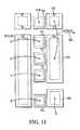
- FIG. 13illustrates a schematic diagram for a dynamic OPL logic circuit fabricated according to the present invention.
- FIG. 14illustrates a processing system having ultra-thin vertical transistors with strained silicon channels formed according to embodiments of the present invention.
- substrateused in the following description may include any semiconductor-based structure that has a silicon surface. Structure must be understood to include silicon, silicon-on insulator (SOI), silicon-on sapphire (SOS), doped and undoped semiconductors, epitaxial layers of silicon supported by a base semiconductor foundation, and other semiconductor structures.
- SOIsilicon-on insulator
- SOSsilicon-on sapphire
- the semiconductoralso need not be silicon-based.
- the semiconductorcould be silicon-germanium, germanium, or gallium arsenide.
- the present inventionprovides a method for the fabrication of integrated CMOS output prediction logic (OPL) circuits with very fast speed and decreased noise sensitivity.
- the very fast output prediction logic (OPL) circuitscomprise CMOS gate arrays with ultra-thin vertical NMOS transistors having relaxed silicon germanium (SiGe) body regions and strained silicon channels.
- Each of the ultra-thin vertical NMOS transistorscomprises a relaxed silicon germanium (SiGe) body region having a graded germanium (Ge) content and a strained silicon channel in contact with the relaxed silicon germanium (SiGe) body region.
- CMOS gate arrays with the ultra-thin vertical NMOS transistors having relaxed silicon germanium (SiGe) body regions and strained silicon channels of the present inventionmay be employed in the fabrication of output prediction logic (OPL) circuits, for example, pseudo-NMOS OPL circuits and dynamic OPL circuits.
- OPLoutput prediction logic
- FIGS. 2-10illustrate the fabrication of ultra-thin vertical NMOS transistors 300 a, 300 b ( FIG. 10 ) with relaxed silicon germanium (SiGe) body regions having a graded germanium content and with strained silicon channels.
- the fabrication of the ultra-thin vertical NMOS transistors 300 a, 300 b of FIG. 10requires steps which are similar in part with those employed in the fabrication of vertical PMOS and NMOS transistors, described before in the literature and which will not be described in detail below.
- U.S. Pat. No. 6,072,209 to Noble et al.and U.S. Pat. No.
- FIG. 2illustrates a semiconductor substrate 100 and a first source/drain layer 102 formed over the semiconductor substrate 100 .
- the semiconductor substrate 100may be any of the following three different types of substrates:
- SIMOXSeparatation by IMplanted OXygen
- a subsequent anneal stepforms a buried oxide layer into the substrate.
- an additional layer of epitaxial siliconis usually deposited to obtain a sufficiently thick silicon layer on which to form the desired device.
- a substrate of islands of silicon on insulatorcan be formed, for example, by directionally etching a silicon substrate to form a plurality of trenches between protruding silicon rows; forming a nitride cap on the silicon rows, extending partway down the sides of the trenches; isotropically etching the trenches to partially undercut the silicon rows; and oxidizing the substrate to fully undercut the silicon rows.
- the semiconductor substrate 100will be made in this application as to p-type silicon substrate 100 .
- the first source/drain layer 102may be either an n+ silicon source/drain layer 102 (for NMOS transistors) or a p+ silicon source/drain layer 102 (for PMOS transistors), for the purposes of the present invention, the first source/drain layer 102 of FIG. 2 would be considered an n+ silicon source/drain layer 102 .
- the n+ silicon source/drain layer 102may be formed by ion implantation, epitaxial growth, or a combination of these techniques. Vertical NMOS transistors with strained silicon channels and relaxed silicon germanium (SiGe) body regions will be formed on the n+ silicon source/drain layer 102 in accordance with embodiments of the present invention and as illustrated in more detail below.
- a relaxed silicon germanium (SiGe) layer 105 with a graded germanium contentis next formed over the first source/drain layer 102 to a thickness of about 2,000 Angstroms to about 40,000 Angstroms.
- the relaxed silicon germanium (SiGe) layer 105is epitaxially grown by an ultra high vacuum chemical vapor deposition (UHVCVD) method and using a linear graded buffer layer technique, as described by K. Rim et al. in Strained Si NMOSFETs for High Performance CMOS Technology, Symp. on VLSI Tech. Digest of Technical Papers, p. 59 (2001) and by K. Rim, et al. in Fabrication and Analysis of Deep Submicron Strained - Si N - MOSFET's, IEEE Trans. Electron. Devices, 47, p. 1406 (2000), the disclosures of which are incorporated by reference herein.
- the germanium (Ge) content in the silicon germanium (SiGe) layer 105is graded in steps using a linear graded buffer layer technique, by increasing the germanium content from 0 to about 20% over a thickness of about 1.5 ⁇ m.
- the fully relaxed silicon germanium (SiGe) layer 105 with the graded germanium contentis capped with a 7,000 Angstroms thick relaxed silicon germanium (SiGe) layer with a constant germanium content of about 20%.
- Dichlorosilane and germaneare used as the silicon and germanium source precursors at growth temperatures of about 700° C. to about 750° C.
- both the thickness of the relaxed silicon germanium (SiGe) layer 105 and the germanium (Ge) content in the silicon germanium (SiGe) layerare verified by cross-sectional TEM, Rutherford back-scattering and Raman spectroscopy. X-ray diffraction analysis quantified the germanium (Ge) content to about 15% and 20%.
- the relaxed silicon germanium (SiGe) layer 105 with graded germanium (Ge) contentacts as a buffer layer for strained silicon (Si) layer 120 (FIG. 7 ), which will form a strained silicon channel for a vertical NMOS transistor fabricated according to the present invention.
- a second source/drain layer 106is formed over the relaxed silicon germanium (SiGe) layer 105 with graded germanium content.
- the second source/drain layer 106may be formed by ion implantation, epitaxial growth, or a combination of these techniques.
- a photoresistis subsequently applied and selectively exposed to provide a mask for the directional etching of trenches 109 ( FIGS. 5 , 6 ) by reactive ion etching (RIE), for example.
- RIEreactive ion etching
- the directional etchingresults in the formation of a plurality of pillars or column bars 150 ( FIG. 5 ) each comprising a stack of the first source/drain layer 102 , the relaxed silicon germanium (SiGe) layer 105 with graded germanium content and the second source/drain layer 106 .
- the resulting pillars or column bars 150provide first and second source/drain regions 102 and 106 , respectively, and silicon germanium (SiGe) body region 105 for NMOS transistors 300 a, 300 b (FIG. 10 ).
- Oxide layer 104( FIG. 6 ) is formed on the surface of the p+ silicon substrate 100 and the first source/drain layer 102 to surround the NMOS transistors 300 a, 300 b ( FIG. 10 ) with relaxed silicon germanium (SiGe) body regions 105 having graded germanium content.
- the previously-mentioned processing steps for the fabrication of ultra-thin vertical pillars or column bars 150are similar in part to the ones described in U.S. Pat. No.
- a strained silicon layer of about 200 Angstroms to about 2,000 Angstromsis formed on each side of the relaxed silicon germanium (SiGe) body region 105 with graded germanium content and directionally etched to leave strained silicon channel layer 120 ( FIG. 7 ) on two opposing sidewalls of the pillars.
- the strained silicon channel layer 120may be epitaxially grown by an ultra high vacuum chemical vapor deposition (UHVCVD) method at about 1000° C.
- UHVCVDultra high vacuum chemical vapor deposition
- the subband splittingis larger in strained silicon (Si) than in unstrained silicon because of the strain-induced band splitting in addition to that provided by quantum confinement.
- the ground level splitting (E 0 (d 4 ) ⁇ E 0 (d 2 )) in an MOS inversion layer at 1 MV/cm transverse fieldis about 120 and about 250 meV for unstrained and strained silicon, respectively.
- K. Rim et al.have demonstrated that the increase in energy splitting reduces intervalley scattering and enhances NMOSFET mobility for vertical fields higher than about 1 MV/cm.
- biaxial tensile strain in thin silicon layers grown pseudomorphically on relaxed silicon germanium layerssplits the 6-fold degeneracy in a silicon conduction band. The splitting causes the 2-fold degenerate ( ⁇ 2 ) valleys to be preferentially populated, suppressing intervalley scattering.
- a thick oxide layer 130 of about 1,000 Angstroms to about 20,000 Angstromsis next formed over the strained silicon layer 120 .
- Another masking stepcan be employed to isotropically etch the oxide layer 130 off of some of the sidewalls of pillars or column bars 150 and leave the oxide only on one sidewall of each column bar 150 as required for particular configurations.
- the above-described stepsare similar in part to the ones detailed in U.S. Pat. No. 6,150,687 to Noble et al. and incorporated by reference in this application.
- a gate oxide layer 140is formed on the exposed sidewalls of the strained silicon layer 120 .
- the gate oxide 140may be formed, for example, by thermal growth, or by dry oxidation at high temperatures under an oxygen atmosphere, or by thermally growing an oxynitride using a nitrogen and oxygen source.
- the drain and source regions of the NMOS transistors 300 a, 300 bare in the strained silicon channel layer 120 along the sidewalls of each pillar 105 .
- the present inventioncontemplates the formation of ultra-thin body transistors with strained silicon channels which include other types of gate structures, such as for example, horizontal gate structures as described in U.S. Pat. No. 6,150,687 to Noble et al., or horizontal replacement gate structures, a variation of U.S. Pat. No. 6,150,687 to Noble et al described in U.S. patent application Ser. No. 09/596,266 filed Jun. 16, 2000.
- FIG. 10illustrates the formation of transistor gates 170 and wiring contacts 180 , 182 .
- the transistor gates 170which may be formed of polysilicon for example, are vertically oriented gates and are associated with a side of the pillars 150 .
- the transistor gates 170 of FIG. 10may be formed, for example, by a deposition method such as chemical vapor deposition (CVD) at a temperature of about 550° C. to about 650° C. and a pressure of less than about 2 Torr.
- CVDchemical vapor deposition
- the top portions of the CVD deposited polysilicon material located above the second source/drain layer 105 ( FIG. 10 )are then removed by CMP, for example, to form the transistor gates 170 .
- FIG. 10also illustrates the thick oxide layer 130 formed, as described above, on an opposing side of each of the pillar 150 for isolating the transistor gate 170 from neighboring pillars.
- the ultra-thin vertical NMOS transistors 300 a, 300 b with relaxed silicon germanium (SiGe) body regions 105 and strained silicon channels 120may be employed in the fabrication of vertical gate array structures comprising a plurality of such ultra-thin vertical NMOS transistors with strained silicon channels, with or without PMOS transistors.
- the ultra-thin vertical NMOS transistors 300 a, 300 b with strained silicon channel 120may be also employed in the fabrication of gate array structures comprising other conventional planar structures, as described in the literature and formed by known conventional techniques, in addition to the vertical gate structures of the present invention.
- FIG. 11illustrates a logic gate implementation using ultra-thin vertical NMOS transistors having relaxed silicon germanium (SiGe) body regions with graded germanium content and strained silicon channels fabricated according to embodiments of the present invention.
- the logic gate implementation of FIG. 11is a dynamic 3-input NOR gate shown as circuit 500 of FIG. 13 .
- a number of logic inputs A, B, Care coupled to gates 351 for a number of ultra-thin vertical NMOS transistors with relaxed silicon germanium (SiGe) body regions and strained silicon channels formed according to the present invention and illustrated as block 350 .
- FIG. 11further illustrates a clock input coupled to gate 331 of a PMOS transistor 330 .
- the circuit shown in FIG. 11comprises the PMOS transistor 330 coupled between a power supply (e.g. Vdd) and an output which precharges the output high during a precharge stage and prior to the arrival of a number of input signals as the number of logic inputs A, B and C.
- An output 380is illustrated as coupled to both the PMOS transistor 330 and the number of ultra-thin vertical NMOS transistors with relaxed silicon germanium (SiGe) body regions with graded germanium content and strained silicon channels shown as the block 350 .
- the output 380will be coupled to one of the number of inputs of a subsequent static logic circuit portion (not shown) as part of a CMOS logic circuit.
- FIG. 12illustrates the implementation of the ultra-thin vertical NMOS transistors 300 a, 300 b with silicon germanium (SiGe) body regions and strained silicon channels in the fabrication of a pseudo-NMOS output prediction logic (OPL) circuit 400 .
- OPLoutput prediction logic
- the pseudo-NMOS OPL circuit 400 of FIG. 12has an enable NMOS transistor at the bottom of the gate.
- the clock (clk)When the clock (clk) is low, the gate is disabled, with the output being charged to a logic “1.”
- the gateWhen the clock goes high, the gate is enabled and becomes a pseudo-NMOS gate.
- the pull-up PMOSserves both to precharge the gate and to correct a high output when it glitches.
- FIG. 13illustrates a dynamic output prediction logic (OPL) circuit 500 in which the PMOS transistor is clocked to precharge the output high.
- OPLdynamic output prediction logic
- the nodewill either be left high, or will be discharged to ground potential.
- These gateswork only on a dynamic basis, by charge storage on capacitive nodes.
- the OPL-dynamic gatelooks similar to a domino gate, but with the output inverter missing. The gate precharges high, and the keeper transistor, if sized sufficiently large, will enable the output node to recover from glitches.
- the ultra-thin vertical NMOS transistors 300 a, 300 b ( FIG. 10 ) of the present inventionmay be also incorporated in other semiconductor device, including various processor system components, such as for example, a central processing unit (CPU), or in any of the various types of memory devices, such as for example, RAM, ROM, and others. They may also be used in any type of integrated circuit controller for a floppy disk, a hard disk, a ZIP, or a CD-ROM disk.
- FIG. 14illustrates an exemplary processing system 900 which may utilize the ultra-thin vertical NMOS transistors 300 a, 300 b of the present invention.
- the processing system 900includes one or more processors 901 coupled to a local bus 904 .
- a memory controller 902 and a primary bus bridge 903are also coupled the local bus 904 .
- the processing system 900may include multiple memory controllers 902 and/or multiple primary bus bridges 903 .
- the memory controller 902 and the primary bus bridge 903may be integrated as a single device 906 .
- the memory controller 902is also coupled to one or more memory buses 907 .
- Each memory busaccepts memory components 908 which include at least one memory device 100 comprising at least one ultra-thin vertical NMOS transistor, such as the ultra-thin vertical NMOS transistors 300 a, 300 b of the present invention.
- the memory components 908may be a memory card or a memory module. Examples of memory modules include single inline memory modules (SIMMs) and dual inline memory modules (DIMMs).
- the memory components 908may include one or more additional devices 909 .
- the additional device 909might be a configuration memory, such as a serial presence detect (SPD) memory.
- the memory controller 902may also be coupled to a cache memory 905 .
- the cache memory 905may be the only cache memory in the processing system. Alternatively, other devices, for example, processors 901 may also include cache memories, which may form a cache hierarchy with cache memory 905 . If the processing system 900 include peripherals or controllers which are bus masters or which support direct memory access (DMA), the memory controller 902 may implement a cache coherency protocol. If the memory controller 902 is coupled to a plurality of memory buses 907 , each memory bus 907 may be operated in parallel, or different address ranges may be mapped to different memory buses 907 .
- DMAdirect memory access
- the primary bus bridge 903is coupled to at least one peripheral bus 910 .
- Various devicessuch as peripherals or additional bus bridges may be coupled to the peripheral bus 910 . These devices may include a storage controller 911 , an miscellaneous I/O device 914 , a secondary bus bridge 915 , a multimedia processor 918 , and an legacy device interface 920 .
- the primary bus bridge 903may also coupled to one or more special purpose high speed ports 922 . In a personal computer, for example, the special purpose port might be the Accelerated Graphics Port (AGP), used to couple a high performance video card to the processing system 900 .
- AGPAccelerated Graphics Port
- the storage controller 911couples one or more storage devices 913 , via a storage bus 912 , to the peripheral bus 910 .
- the storage controller 911may be a SCSI controller and storage devices 913 may be SCSI discs.
- the I/O device 914may be any sort of peripheral.
- the I/O device 914may be an local area network interface, such as an Ethernet card.
- the secondary bus bridgemay be used to interface additional devices via another bus to the processing system.
- the secondary bus bridgemay be an universal serial port (USB) controller used to couple USB devices 917 via to the processing system 900 .
- the multimedia processor 918may be a sound card, a video capture card, or any other type of media interface, which may also be coupled to one additional devices such as speakers 919 .
- the legacy device interface 920is used to couple legacy devices, for example, older styled keyboards and mice, to the processing system 900 .
- the processing system 900 illustrated in FIG. 14is only an exemplary processing system with which the invention may be used. While FIG. 14 illustrates a processing architecture especially suitable for a general purpose computer, such as a personal computer or a workstation, it should be recognized that well known modifications can be made to configure the processing system 900 to become more suitable for use in a variety of applications. For example, many electronic devices which require processing may be implemented using a simpler architecture which relies on a CPU 901 coupled to memory components 908 and/or memory devices 100 comprising at least one ultra-thin vertical NMOS transistors 300 a, 300 b.
- These electronic devicesmay include, but are not limited to audio/video processors and recorders, gaming consoles, digital television sets, wired or wireless telephones, navigation devices (including system based on the global positioning system (GPS) and/or inertial navigation), and digital cameras and/or recorders.
- the modificationsmay include, for example, elimination of unnecessary components, addition of specialized devices or circuits, and/or integration of a plurality of devices.
Landscapes
- Metal-Oxide And Bipolar Metal-Oxide Semiconductor Integrated Circuits (AREA)
- Thin Film Transistor (AREA)
Abstract
Description
- (i) lightly doped p-type;
- (ii) silicon on insulator substrates, such as SIMOX, for example; and
- (iii) islands of silicon on insulator formed by techniques such as those described in U.S. Pat. No. 5,691,230 to Forbes, the disclosure of which is incorporated by reference herein.
Claims (19)
Priority Applications (3)
| Application Number | Priority Date | Filing Date | Title |
|---|---|---|---|
| US10/164,611US6900521B2 (en) | 2002-06-10 | 2002-06-10 | Vertical transistors and output prediction logic circuits containing same |
| US10/759,107US6998311B2 (en) | 2002-06-10 | 2004-01-20 | Methods of forming output prediction logic circuits with ultra-thin vertical transistors |
| US11/080,443US7217974B2 (en) | 2002-06-10 | 2005-03-16 | Output prediction logic circuits with ultra-thin vertical transistors and methods of formation |
Applications Claiming Priority (1)
| Application Number | Priority Date | Filing Date | Title |
|---|---|---|---|
| US10/164,611US6900521B2 (en) | 2002-06-10 | 2002-06-10 | Vertical transistors and output prediction logic circuits containing same |
Related Child Applications (2)
| Application Number | Title | Priority Date | Filing Date |
|---|---|---|---|
| US10/759,107DivisionUS6998311B2 (en) | 2002-06-10 | 2004-01-20 | Methods of forming output prediction logic circuits with ultra-thin vertical transistors |
| US11/080,443ContinuationUS7217974B2 (en) | 2002-06-10 | 2005-03-16 | Output prediction logic circuits with ultra-thin vertical transistors and methods of formation |
Publications (2)
| Publication Number | Publication Date |
|---|---|
| US20030227072A1 US20030227072A1 (en) | 2003-12-11 |
| US6900521B2true US6900521B2 (en) | 2005-05-31 |
Family
ID=29710247
Family Applications (3)
| Application Number | Title | Priority Date | Filing Date |
|---|---|---|---|
| US10/164,611Expired - LifetimeUS6900521B2 (en) | 2002-06-10 | 2002-06-10 | Vertical transistors and output prediction logic circuits containing same |
| US10/759,107Expired - Fee RelatedUS6998311B2 (en) | 2002-06-10 | 2004-01-20 | Methods of forming output prediction logic circuits with ultra-thin vertical transistors |
| US11/080,443Expired - LifetimeUS7217974B2 (en) | 2002-06-10 | 2005-03-16 | Output prediction logic circuits with ultra-thin vertical transistors and methods of formation |
Family Applications After (2)
| Application Number | Title | Priority Date | Filing Date |
|---|---|---|---|
| US10/759,107Expired - Fee RelatedUS6998311B2 (en) | 2002-06-10 | 2004-01-20 | Methods of forming output prediction logic circuits with ultra-thin vertical transistors |
| US11/080,443Expired - LifetimeUS7217974B2 (en) | 2002-06-10 | 2005-03-16 | Output prediction logic circuits with ultra-thin vertical transistors and methods of formation |
Country Status (1)
| Country | Link |
|---|---|
| US (3) | US6900521B2 (en) |
Cited By (35)
| Publication number | Priority date | Publication date | Assignee | Title |
|---|---|---|---|---|
| US20050156230A1 (en)* | 2002-06-10 | 2005-07-21 | Leonard Forbes | Output prediction logic circuits with ultra-thin vertical transistors and methods of formation |
| US20050164448A1 (en)* | 2004-01-23 | 2005-07-28 | Elpida Memory, Inc. | Method for manufacturing a semiconductor device |
| US20050263753A1 (en)* | 2003-12-05 | 2005-12-01 | Advanced Micro Devices, Inc. | Semiconductor substrate layer configured for inducement of compressive or expansive force |
| US20060189078A1 (en)* | 2004-05-26 | 2006-08-24 | Werner Juengling | Semiconductor structures and memory device constructions |
| US20060211194A1 (en)* | 2004-12-13 | 2006-09-21 | Haller Gordon A | Methods of reducing floating body effect |
| US7120046B1 (en) | 2005-05-13 | 2006-10-10 | Micron Technology, Inc. | Memory array with surrounding gate access transistors and capacitors with global and staggered local bit lines |
| US20060258109A1 (en)* | 2004-09-01 | 2006-11-16 | Werner Juengling | DRAM cells with vertical transistors |
| US20060258084A1 (en)* | 2004-09-02 | 2006-11-16 | Tang Sanh D | Vertical transistors |
| US20070018223A1 (en)* | 2005-07-25 | 2007-01-25 | Micron Technology Inc. | Dram including a vertical surround gate transistor |
| US20070045721A1 (en)* | 2005-08-29 | 2007-03-01 | Micron Technology, Inc. | Ultra-thin body vertical tunneling transistor |
| US20070066019A1 (en)* | 2005-07-06 | 2007-03-22 | Leonard Forbes | Surround gate access transistors with grown ultra-thin bodies |
| US20070187683A1 (en)* | 2006-02-16 | 2007-08-16 | Micron Technology, Inc. | Localized compressive strained semiconductor |
| US20070205443A1 (en)* | 2006-03-02 | 2007-09-06 | Werner Juengling | Vertical gated access transistor |
| US20070205438A1 (en)* | 2006-03-02 | 2007-09-06 | Werner Juengling | Masking process for simultaneously patterning separate regions |
| US20070215940A1 (en)* | 2006-03-16 | 2007-09-20 | Spansion Llc | Vertical semiconductor device |
| US20080029832A1 (en)* | 2006-08-03 | 2008-02-07 | Micron Technology, Inc. | Bonded strained semiconductor with a desired surface orientation and conductance direction |
| US20080042211A1 (en)* | 2006-08-18 | 2008-02-21 | Micron Technology, Inc. | Strained semiconductor channels and methods of formation |
| US20080048258A1 (en)* | 2006-08-25 | 2008-02-28 | De Fresart Edouard D | Trench power device and method |
| US7371627B1 (en) | 2005-05-13 | 2008-05-13 | Micron Technology, Inc. | Memory array with ultra-thin etched pillar surround gate access transistors and buried data/bit lines |
| US20080162876A1 (en)* | 2006-12-28 | 2008-07-03 | International Business Machines Corporation | dedicated hardware processor for structured query language (sql) transactions |
| US20080233725A1 (en)* | 2007-03-23 | 2008-09-25 | Micron Technology, Inc. | Methods for stressing semiconductor material structures to improve electron and/or hole mobility of transistor channels fabricated therefrom, and semiconductor devices including such structures |
| US20080237636A1 (en)* | 2007-03-29 | 2008-10-02 | Been-Yih Jin | Transistor having tensile strained channel and system including same |
| US20080277734A1 (en)* | 2007-05-08 | 2008-11-13 | Micron Technology, Inc. | Implantation processes for straining transistor channels of semiconductor device structures and semiconductor devices with strained transistor channels |
| US7482190B2 (en) | 2003-05-07 | 2009-01-27 | Micron Technology, Inc. | Micromechanical strained semiconductor by wafer bonding |
| US20100019276A1 (en)* | 2008-07-25 | 2010-01-28 | Hynix Semiconductor Inc. | All around gate type semiconductor device and method of manufacturing the same |
| US7696567B2 (en) | 2005-08-31 | 2010-04-13 | Micron Technology, Inc | Semiconductor memory device |
| US20100244127A1 (en)* | 2004-10-07 | 2010-09-30 | Ihsiu Ho | Bandgap engineered mos-gated power transistors |
| US7935999B2 (en) | 2005-09-01 | 2011-05-03 | Micron Technology, Inc. | Memory device |
| US7939409B2 (en) | 2005-09-01 | 2011-05-10 | Micron Technology, Inc. | Peripheral gate stacks and recessed array gates |
| US7977236B2 (en) | 2005-09-01 | 2011-07-12 | Micron Technology, Inc. | Method of forming a transistor gate of a recessed access device, method of forming a recessed transistor gate and a non-recessed transistor gate, and method of fabricating an integrated circuit |
| US8101497B2 (en) | 2008-09-11 | 2012-01-24 | Micron Technology, Inc. | Self-aligned trench formation |
| US8274106B2 (en) | 2004-07-20 | 2012-09-25 | Micron Technology, Inc. | DRAM layout with vertical FETs and method of formation |
| US9287271B2 (en) | 2011-08-23 | 2016-03-15 | Micron Technology, Inc. | Vertical transistor devices, memory arrays, and methods of forming vertical transistor devices |
| US10515801B2 (en) | 2007-06-04 | 2019-12-24 | Micron Technology, Inc. | Pitch multiplication using self-assembling materials |
| US10985073B2 (en) | 2019-07-08 | 2021-04-20 | International Business Machines Corporation | Vertical field effect transistor replacement metal gate fabrication |
Families Citing this family (55)
| Publication number | Priority date | Publication date | Assignee | Title |
|---|---|---|---|---|
| US20040023874A1 (en)* | 2002-03-15 | 2004-02-05 | Burgess Catherine E. | Therapeutic polypeptides, nucleic acids encoding same, and methods of use |
| US6383924B1 (en) | 2000-12-13 | 2002-05-07 | Micron Technology, Inc. | Method of forming buried conductor patterns by surface transformation of empty spaces in solid state materials |
| JP2002232075A (en)* | 2001-01-31 | 2002-08-16 | Ando Electric Co Ltd | Tunable light source |
| US7142577B2 (en) | 2001-05-16 | 2006-11-28 | Micron Technology, Inc. | Method of forming mirrors by surface transformation of empty spaces in solid state materials and structures thereon |
| US6898362B2 (en)* | 2002-01-17 | 2005-05-24 | Micron Technology Inc. | Three-dimensional photonic crystal waveguide structure and method |
| US20030048656A1 (en)* | 2001-08-28 | 2003-03-13 | Leonard Forbes | Four terminal memory cell, a two-transistor sram cell, a sram array, a computer system, a process for forming a sram cell, a process for turning a sram cell off, a process for writing a sram cell and a process for reading data from a sram cell |
| JP3597831B2 (en)* | 2002-07-01 | 2004-12-08 | 株式会社東芝 | Field effect transistor and method of manufacturing the same |
| US6972599B2 (en)* | 2002-08-27 | 2005-12-06 | Micron Technology Inc. | Pseudo CMOS dynamic logic with delayed clocks |
| US7198974B2 (en) | 2003-03-05 | 2007-04-03 | Micron Technology, Inc. | Micro-mechanically strained semiconductor film |
| US7041575B2 (en)* | 2003-04-29 | 2006-05-09 | Micron Technology, Inc. | Localized strained semiconductor on insulator |
| US6987037B2 (en) | 2003-05-07 | 2006-01-17 | Micron Technology, Inc. | Strained Si/SiGe structures by ion implantation |
| US7501329B2 (en) | 2003-05-21 | 2009-03-10 | Micron Technology, Inc. | Wafer gettering using relaxed silicon germanium epitaxial proximity layers |
| US7662701B2 (en) | 2003-05-21 | 2010-02-16 | Micron Technology, Inc. | Gettering of silicon on insulator using relaxed silicon germanium epitaxial proximity layers |
| US7008854B2 (en) | 2003-05-21 | 2006-03-07 | Micron Technology, Inc. | Silicon oxycarbide substrates for bonded silicon on insulator |
| US7001788B2 (en)* | 2003-05-29 | 2006-02-21 | Applied Materials, Inc. | Maskless fabrication of waveguide mirrors |
| US6929984B2 (en) | 2003-07-21 | 2005-08-16 | Micron Technology Inc. | Gettering using voids formed by surface transformation |
| US7439158B2 (en) | 2003-07-21 | 2008-10-21 | Micron Technology, Inc. | Strained semiconductor by full wafer bonding |
| US7153753B2 (en) | 2003-08-05 | 2006-12-26 | Micron Technology, Inc. | Strained Si/SiGe/SOI islands and processes of making same |
| US20050266632A1 (en)* | 2004-05-26 | 2005-12-01 | Yun-Hsiu Chen | Integrated circuit with strained and non-strained transistors, and method of forming thereof |
| US7247570B2 (en) | 2004-08-19 | 2007-07-24 | Micron Technology, Inc. | Silicon pillars for vertical transistors |
| US7229895B2 (en)* | 2005-01-14 | 2007-06-12 | Micron Technology, Inc | Memory array buried digit line |
| US7465972B2 (en)* | 2005-01-21 | 2008-12-16 | Taiwan Semiconductor Manufacturing Company, Ltd. | High performance CMOS device design |
| US7268362B2 (en) | 2005-02-25 | 2007-09-11 | Taiwan Semiconductor Manufacturing Company, Ltd. | High performance transistors with SiGe strain |
| KR100673105B1 (en)* | 2005-03-31 | 2007-01-22 | 주식회사 하이닉스반도체 | Vertical transistors in semiconductor devices and methods of forming them |
| US7811935B2 (en) | 2006-03-07 | 2010-10-12 | Micron Technology, Inc. | Isolation regions and their formation |
| US7514726B2 (en)* | 2006-03-21 | 2009-04-07 | The United States Of America As Represented By The Aministrator Of The National Aeronautics And Space Administration | Graded index silicon geranium on lattice matched silicon geranium semiconductor alloy |
| US7323392B2 (en)* | 2006-03-28 | 2008-01-29 | Taiwan Semiconductor Manufacturing Company, Ltd. | High performance transistor with a highly stressed channel |
| US8354311B2 (en)* | 2006-04-04 | 2013-01-15 | Micron Technology, Inc. | Method for forming nanofin transistors |
| US7491995B2 (en) | 2006-04-04 | 2009-02-17 | Micron Technology, Inc. | DRAM with nanofin transistors |
| US7425491B2 (en)* | 2006-04-04 | 2008-09-16 | Micron Technology, Inc. | Nanowire transistor with surrounding gate |
| US20070228491A1 (en)* | 2006-04-04 | 2007-10-04 | Micron Technology, Inc. | Tunneling transistor with sublithographic channel |
| US8734583B2 (en)* | 2006-04-04 | 2014-05-27 | Micron Technology, Inc. | Grown nanofin transistors |
| US8558278B2 (en)* | 2007-01-16 | 2013-10-15 | Taiwan Semiconductor Manufacturing Company, Ltd. | Strained transistor with optimized drive current and method of forming |
| US7769135B2 (en)* | 2007-10-18 | 2010-08-03 | The United States Of America As Represented By The Administrator Of The National Aeronautics And Space Administration | X-ray diffraction wafer mapping method for rhombohedral super-hetero-epitaxy |
| US7825465B2 (en)* | 2007-12-13 | 2010-11-02 | Fairchild Semiconductor Corporation | Structure and method for forming field effect transistor with low resistance channel region |
| KR100960928B1 (en)* | 2008-01-02 | 2010-06-07 | 주식회사 하이닉스반도체 | Vertical transistors and their formation |
| US7943961B2 (en)* | 2008-03-13 | 2011-05-17 | Taiwan Semiconductor Manufacturing Company, Ltd. | Strain bars in stressed layers of MOS devices |
| KR100946084B1 (en)* | 2008-03-27 | 2010-03-10 | 주식회사 하이닉스반도체 | Vertical transistors in semiconductor devices and methods of forming them |
| US7808051B2 (en)* | 2008-09-29 | 2010-10-05 | Taiwan Semiconductor Manufacturing Company, Ltd. | Standard cell without OD space effect in Y-direction |
| US8222657B2 (en)* | 2009-02-23 | 2012-07-17 | The Penn State Research Foundation | Light emitting apparatus |
| SG165252A1 (en)* | 2009-03-25 | 2010-10-28 | Unisantis Electronics Jp Ltd | Semiconductor device and production method therefor |
| CN102751331B (en)* | 2012-07-16 | 2015-07-22 | 西安电子科技大学 | Strain SiGe square-in-square type channel NMOS (N-channel Metal Oxide Semiconductor) integrated device and preparation method thereof |
| CN102832218B (en)* | 2012-07-16 | 2015-03-04 | 西安电子科技大学 | Strain SiGe vertical CMOS (complementary metal-oxide-semiconductor transistor) integrated device and preparation method thereof |
| US9614026B2 (en) | 2013-03-13 | 2017-04-04 | The United States Of America As Represented By The Administrator Of The National Aeronautics And Space Administration | High mobility transport layer structures for rhombohedral Si/Ge/SiGe devices |
| US9859286B2 (en) | 2014-12-23 | 2018-01-02 | International Business Machines Corporation | Low-drive current FinFET structure for improving circuit density of ratioed logic in SRAM devices |
| US10211338B2 (en)* | 2015-09-03 | 2019-02-19 | Globalfoundries Singapore Pte. Ltd. | Integrated circuits having tunnel transistors and methods for fabricating the same |
| WO2017052650A1 (en)* | 2015-09-25 | 2017-03-30 | Intel Corporation | Long channel mos transistors for low leakage applications on a short channel cmos chip |
| US9614077B1 (en) | 2016-03-03 | 2017-04-04 | International Business Machines Corporation | Vertical finfet with strained channel |
| US11018254B2 (en)* | 2016-03-31 | 2021-05-25 | International Business Machines Corporation | Fabrication of vertical fin transistor with multiple threshold voltages |
| US11195764B2 (en)* | 2018-04-04 | 2021-12-07 | International Business Machines Corporation | Vertical transport field-effect transistors having germanium channel surfaces |
| CN108766967B (en)* | 2018-05-23 | 2021-05-28 | 燕山大学 | A kind of planar composite strained Si/SiGe CMOS device and preparation method |
| US11107817B2 (en) | 2019-03-11 | 2021-08-31 | Micron Technology, Inc. | Integrated assemblies comprising hydrogen diffused within two or more different semiconductor materials, and methods of forming integrated assemblies |
| DE102021108598A1 (en) | 2020-05-29 | 2021-12-02 | Taiwan Semiconductor Manufacturing Company, Ltd. | HETEROSTRUCTURAL OXIDE SEMICONDUCTOR TRANSISTOR WITH VERTICAL GATE-ALL-AROUND (VGAA) AND PROCESS FOR THE PRODUCTION OF IT |
| US11569244B2 (en) | 2020-05-29 | 2023-01-31 | Taiwan Semiconductor Manufacturing Company Limited | Vertical heterostructure semiconductor memory cell and methods for making the same |
| US11848357B2 (en)* | 2022-01-24 | 2023-12-19 | International Business Machines Corporation | Strained superlattice |
Citations (13)
| Publication number | Priority date | Publication date | Assignee | Title |
|---|---|---|---|---|
| US4569032A (en)* | 1983-12-23 | 1986-02-04 | At&T Bell Laboratories | Dynamic CMOS logic circuits for implementing multiple AND-functions |
| US5451800A (en)* | 1992-12-02 | 1995-09-19 | International Business Machines Corporation | Metal oxide semiconductor heterojunction field effect transistor (MOSHFET) |
| US5714777A (en)* | 1997-02-19 | 1998-02-03 | International Business Machines Corporation | Si/SiGe vertical junction field effect transistor |
| US5821577A (en)* | 1991-01-10 | 1998-10-13 | International Business Machines Corporation | Graded channel field effect transistor |
| US6191432B1 (en)* | 1996-09-02 | 2001-02-20 | Kabushiki Kaisha Toshiba | Semiconductor device and memory device |
| US6313487B1 (en)* | 2000-06-15 | 2001-11-06 | Board Of Regents, The University Of Texas System | Vertical channel floating gate transistor having silicon germanium channel layer |
| US20020125497A1 (en)* | 2001-03-02 | 2002-09-12 | Fitzgerald Eugene A. | Relaxed silicon germanium platform for high speed CMOS electronics and high speed analog circuits |
| US20020168864A1 (en)* | 2001-04-04 | 2002-11-14 | Zhiyuan Cheng | Method for semiconductor device fabrication |
| US20020179946A1 (en)* | 2000-10-19 | 2002-12-05 | Yoshiro Hara | P-channel field-effect transistor |
| US20030057439A1 (en)* | 2001-08-09 | 2003-03-27 | Fitzgerald Eugene A. | Dual layer CMOS devices |
| US20030068883A1 (en)* | 2000-11-15 | 2003-04-10 | International Business Machines Corporation | Self-aligned silicide (salicide) process for strained silicon MOSFET on SiGe and structure formed thereby |
| US20030201458A1 (en)* | 2002-03-19 | 2003-10-30 | Clark William F. | Strained fin fets structure and method |
| US6744083B2 (en)* | 2001-12-20 | 2004-06-01 | The Board Of Regents, The University Of Texas System | Submicron MOSFET having asymmetric channel profile |
Family Cites Families (20)
| Publication number | Priority date | Publication date | Assignee | Title |
|---|---|---|---|---|
| US5266813A (en)* | 1992-01-24 | 1993-11-30 | International Business Machines Corporation | Isolation technique for silicon germanium devices |
| US5914504A (en)* | 1995-06-16 | 1999-06-22 | Imec Vzw | DRAM applications using vertical MISFET devices |
| JP3535527B2 (en)* | 1997-06-24 | 2004-06-07 | マサチューセッツ インスティテュート オブ テクノロジー | Controlling threading dislocations in germanium-on-silicon using graded GeSi layer and planarization |
| US6323108B1 (en)* | 1999-07-27 | 2001-11-27 | The United States Of America As Represented By The Secretary Of The Navy | Fabrication ultra-thin bonded semiconductor layers |
| JP2003520452A (en)* | 2000-01-20 | 2003-07-02 | アンバーウェーブ システムズ コーポレイション | Strained silicon metal oxide semiconductor field effect transistor |
| AU2001263211A1 (en)* | 2000-05-26 | 2001-12-11 | Amberwave Systems Corporation | Buried channel strained silicon fet using an ion implanted doped layer |
| JP2004523103A (en)* | 2000-12-04 | 2004-07-29 | アンバーウェーブ システムズ コーポレイション | CMOS inverter circuit using strained silicon surface channel MOSFET |
| US20020100942A1 (en)* | 2000-12-04 | 2002-08-01 | Fitzgerald Eugene A. | CMOS inverter and integrated circuits utilizing strained silicon surface channel MOSFETs |
| US6455377B1 (en)* | 2001-01-19 | 2002-09-24 | Chartered Semiconductor Manufacturing Ltd. | Method to form very high mobility vertical channel transistor by selective deposition of SiGe or multi-quantum wells (MQWs) |
| US6646322B2 (en)* | 2001-03-02 | 2003-11-11 | Amberwave Systems Corporation | Relaxed silicon germanium platform for high speed CMOS electronics and high speed analog circuits |
| US6830976B2 (en)* | 2001-03-02 | 2004-12-14 | Amberwave Systems Corproation | Relaxed silicon germanium platform for high speed CMOS electronics and high speed analog circuits |
| US7205604B2 (en)* | 2001-03-13 | 2007-04-17 | International Business Machines Corporation | Ultra scalable high speed heterojunction vertical n-channel MISFETs and methods thereof |
| FR2823010B1 (en)* | 2001-04-02 | 2003-08-15 | St Microelectronics Sa | METHOD FOR MANUFACTURING A VERTICAL TRANSISTOR WITH AN INSULATED GRID WITH A QUADRUPLE CONDUCTION CHANNEL, AND INTEGRATED CIRCUIT COMPRISING SUCH A TRANSISTOR |
| US20020167048A1 (en)* | 2001-05-14 | 2002-11-14 | Tweet Douglas J. | Enhanced mobility NMOS and PMOS transistors using strained Si/SiGe layers on silicon-on-insulator substrates |
| JP3647777B2 (en)* | 2001-07-06 | 2005-05-18 | 株式会社東芝 | Method of manufacturing field effect transistor and integrated circuit element |
| US7202139B2 (en)* | 2002-02-07 | 2007-04-10 | Taiwan Semiconductor Manufacturing Company , Ltd. | MOSFET device with a strained channel |
| US6900521B2 (en)* | 2002-06-10 | 2005-05-31 | Micron Technology, Inc. | Vertical transistors and output prediction logic circuits containing same |
| JP2004076650A (en)* | 2002-08-19 | 2004-03-11 | Denso Corp | Electromagnetic switch for starter |
| US6943407B2 (en)* | 2003-06-17 | 2005-09-13 | International Business Machines Corporation | Low leakage heterojunction vertical transistors and high performance devices thereof |
| US7045401B2 (en)* | 2003-06-23 | 2006-05-16 | Sharp Laboratories Of America, Inc. | Strained silicon finFET device |
- 2002
- 2002-06-10USUS10/164,611patent/US6900521B2/ennot_activeExpired - Lifetime
- 2004
- 2004-01-20USUS10/759,107patent/US6998311B2/ennot_activeExpired - Fee Related
- 2005
- 2005-03-16USUS11/080,443patent/US7217974B2/ennot_activeExpired - Lifetime
Patent Citations (13)
| Publication number | Priority date | Publication date | Assignee | Title |
|---|---|---|---|---|
| US4569032A (en)* | 1983-12-23 | 1986-02-04 | At&T Bell Laboratories | Dynamic CMOS logic circuits for implementing multiple AND-functions |
| US5821577A (en)* | 1991-01-10 | 1998-10-13 | International Business Machines Corporation | Graded channel field effect transistor |
| US5451800A (en)* | 1992-12-02 | 1995-09-19 | International Business Machines Corporation | Metal oxide semiconductor heterojunction field effect transistor (MOSHFET) |
| US6191432B1 (en)* | 1996-09-02 | 2001-02-20 | Kabushiki Kaisha Toshiba | Semiconductor device and memory device |
| US5714777A (en)* | 1997-02-19 | 1998-02-03 | International Business Machines Corporation | Si/SiGe vertical junction field effect transistor |
| US6313487B1 (en)* | 2000-06-15 | 2001-11-06 | Board Of Regents, The University Of Texas System | Vertical channel floating gate transistor having silicon germanium channel layer |
| US20020179946A1 (en)* | 2000-10-19 | 2002-12-05 | Yoshiro Hara | P-channel field-effect transistor |
| US20030068883A1 (en)* | 2000-11-15 | 2003-04-10 | International Business Machines Corporation | Self-aligned silicide (salicide) process for strained silicon MOSFET on SiGe and structure formed thereby |
| US20020125497A1 (en)* | 2001-03-02 | 2002-09-12 | Fitzgerald Eugene A. | Relaxed silicon germanium platform for high speed CMOS electronics and high speed analog circuits |
| US20020168864A1 (en)* | 2001-04-04 | 2002-11-14 | Zhiyuan Cheng | Method for semiconductor device fabrication |
| US20030057439A1 (en)* | 2001-08-09 | 2003-03-27 | Fitzgerald Eugene A. | Dual layer CMOS devices |
| US6744083B2 (en)* | 2001-12-20 | 2004-06-01 | The Board Of Regents, The University Of Texas System | Submicron MOSFET having asymmetric channel profile |
| US20030201458A1 (en)* | 2002-03-19 | 2003-10-30 | Clark William F. | Strained fin fets structure and method |
Cited By (110)
| Publication number | Priority date | Publication date | Assignee | Title |
|---|---|---|---|---|
| US20050156230A1 (en)* | 2002-06-10 | 2005-07-21 | Leonard Forbes | Output prediction logic circuits with ultra-thin vertical transistors and methods of formation |
| US7217974B2 (en)* | 2002-06-10 | 2007-05-15 | Micron Technology, Inc. | Output prediction logic circuits with ultra-thin vertical transistors and methods of formation |
| US7482190B2 (en) | 2003-05-07 | 2009-01-27 | Micron Technology, Inc. | Micromechanical strained semiconductor by wafer bonding |
| US20050263753A1 (en)* | 2003-12-05 | 2005-12-01 | Advanced Micro Devices, Inc. | Semiconductor substrate layer configured for inducement of compressive or expansive force |
| US7265420B2 (en)* | 2003-12-05 | 2007-09-04 | Advanced Micro Devices, Inc. | Semiconductor substrate layer configured for inducement of compressive or expansive force |
| US20050164448A1 (en)* | 2004-01-23 | 2005-07-28 | Elpida Memory, Inc. | Method for manufacturing a semiconductor device |
| US7338876B2 (en)* | 2004-01-23 | 2008-03-04 | Elpida Memory, Inc. | Method for manufacturing a semiconductor device |
| US7391070B2 (en) | 2004-05-26 | 2008-06-24 | Micron Technology, Inc. | Semiconductor structures and memory device constructions |
| US7547949B2 (en) | 2004-05-26 | 2009-06-16 | Micron Technology, Inc. | Semiconductor structures and memory device constructions |
| US7915692B2 (en) | 2004-05-26 | 2011-03-29 | Micron Technology, Inc. | Semiconductor structure including gateline surrounding source and drain pillars |
| US8829602B2 (en) | 2004-05-26 | 2014-09-09 | Micron Technology, Inc. | Integrated circuits and transistor design therefor |
| US20080203453A1 (en)* | 2004-05-26 | 2008-08-28 | Micron Technology, Inc. | Semiconductor structures and memory device constructions |
| US20060189078A1 (en)* | 2004-05-26 | 2006-08-24 | Werner Juengling | Semiconductor structures and memory device constructions |
| US8274106B2 (en) | 2004-07-20 | 2012-09-25 | Micron Technology, Inc. | DRAM layout with vertical FETs and method of formation |
| US8482047B2 (en) | 2004-07-20 | 2013-07-09 | Micron Technology, Inc. | DRAM layout with vertical FETS and method of formation |
| US20060258109A1 (en)* | 2004-09-01 | 2006-11-16 | Werner Juengling | DRAM cells with vertical transistors |
| US20090096000A1 (en)* | 2004-09-01 | 2009-04-16 | Micron Technology, Inc. | Dram cells with vertical transistors |
| US7482229B2 (en)* | 2004-09-01 | 2009-01-27 | Micron Technology, Inc. | DRAM cells with vertical transistors |
| US8097910B2 (en) | 2004-09-01 | 2012-01-17 | Micron Technology, Inc. | Vertical transistors |
| US8372710B2 (en) | 2004-09-01 | 2013-02-12 | Micron Technology, Inc. | Vertical transistors |
| US20100276749A1 (en)* | 2004-09-01 | 2010-11-04 | Micron Technology, Inc. | Vertical transistors |
| US7772633B2 (en) | 2004-09-01 | 2010-08-10 | Micron Technology, Inc. | DRAM cells with vertical transistors |
| US7521322B2 (en) | 2004-09-02 | 2009-04-21 | Micron Technology, Inc. | Vertical transistors |
| US20060258084A1 (en)* | 2004-09-02 | 2006-11-16 | Tang Sanh D | Vertical transistors |
| US20100244127A1 (en)* | 2004-10-07 | 2010-09-30 | Ihsiu Ho | Bandgap engineered mos-gated power transistors |
| US20070128809A1 (en)* | 2004-12-13 | 2007-06-07 | Micron Technology, Inc. | Methods of reducing floating body effect |
| US20070138528A1 (en)* | 2004-12-13 | 2007-06-21 | Micron Technology, Inc. | Memory structure for reduced floating body effect |
| US7183164B2 (en) | 2004-12-13 | 2007-02-27 | Micron Technology, Inc. | Methods of reducing floating body effect |
| US7368344B2 (en) | 2004-12-13 | 2008-05-06 | Micron Technology, Inc. | Methods of reducing floating body effect |
| US7626223B2 (en) | 2004-12-13 | 2009-12-01 | Micron Technology, Inc. | Memory structure for reduced floating body effect |
| US20060211194A1 (en)* | 2004-12-13 | 2006-09-21 | Haller Gordon A | Methods of reducing floating body effect |
| US7525141B1 (en) | 2005-05-13 | 2009-04-28 | Micron Technology, Inc. | Memory array with ultra-thin etched pillar surround gate access transistors and buried data/bit lines |
| US8101992B2 (en) | 2005-05-13 | 2012-01-24 | Micron Technology, Inc. | Memory array with surrounding gate access transistors and capacitors with global and staggered local bit lines |
| US8609523B2 (en) | 2005-05-13 | 2013-12-17 | Micron Technology, Inc. | Method of making a memory array with surrounding gate access transistors and capacitors with global staggered local bit lines |
| US7371627B1 (en) | 2005-05-13 | 2008-05-13 | Micron Technology, Inc. | Memory array with ultra-thin etched pillar surround gate access transistors and buried data/bit lines |
| US8637362B2 (en) | 2005-05-13 | 2014-01-28 | Micron Technology, Inc. | Memory array with ultra-thin etched pillar surround gate access transistors and buried data/bit lines |
| US7120046B1 (en) | 2005-05-13 | 2006-10-10 | Micron Technology, Inc. | Memory array with surrounding gate access transistors and capacitors with global and staggered local bit lines |
| US7510954B1 (en) | 2005-05-13 | 2009-03-31 | Micron Technology, Inc. | Memory array with surrounding gate access transistors and capacitors with global and staggered local bit lines |
| US8350320B2 (en) | 2005-05-13 | 2013-01-08 | Micron Technology, Inc. | Memory array and memory device |
| US8227305B2 (en) | 2005-05-13 | 2012-07-24 | Micron Technology, Inc. | Memory array with ultra-thin etched pillar surround gate access transistors and buried data/bit lines |
| US7910972B2 (en) | 2005-05-13 | 2011-03-22 | Micron Technology, Inc. | Memory array with ultra-thin etched pillar surround gate access transistors and buried data/bit lines |
| US7626219B2 (en) | 2005-07-06 | 2009-12-01 | Micron Technology, Inc. | Surround gate access transistors with grown ultra-thin bodies |
| US7601595B2 (en) | 2005-07-06 | 2009-10-13 | Micron Technology, Inc. | Surround gate access transistors with grown ultra-thin bodies |
| US20070066019A1 (en)* | 2005-07-06 | 2007-03-22 | Leonard Forbes | Surround gate access transistors with grown ultra-thin bodies |
| US8115243B2 (en) | 2005-07-06 | 2012-02-14 | Micron Technology, Inc. | Surround gate access transistors with grown ultra-thin bodies |
| US7888721B2 (en) | 2005-07-06 | 2011-02-15 | Micron Technology, Inc. | Surround gate access transistors with grown ultra-thin bodies |
| US7566620B2 (en) | 2005-07-25 | 2009-07-28 | Micron Technology, Inc. | DRAM including a vertical surround gate transistor |
| US20070018223A1 (en)* | 2005-07-25 | 2007-01-25 | Micron Technology Inc. | Dram including a vertical surround gate transistor |
| US7768051B2 (en) | 2005-07-25 | 2010-08-03 | Micron Technology, Inc. | DRAM including a vertical surround gate transistor |
| US20070045721A1 (en)* | 2005-08-29 | 2007-03-01 | Micron Technology, Inc. | Ultra-thin body vertical tunneling transistor |
| US7745873B2 (en) | 2005-08-29 | 2010-06-29 | Micron Technology, Inc. | Ultra-thin body vertical tunneling transistor |
| US20090014783A1 (en)* | 2005-08-29 | 2009-01-15 | Leonard Forbes | Ultra-thin body vertical tunneling transistor |
| US7439576B2 (en) | 2005-08-29 | 2008-10-21 | Micron Technology, Inc. | Ultra-thin body vertical tunneling transistor |
| US8222105B2 (en) | 2005-08-31 | 2012-07-17 | Micron Technology, Inc. | Methods of fabricating a memory device |
| US8546215B2 (en) | 2005-08-31 | 2013-10-01 | Micron Technology, Inc. | Methods of fabricating a memory device |
| US7696567B2 (en) | 2005-08-31 | 2010-04-13 | Micron Technology, Inc | Semiconductor memory device |
| US8481385B2 (en) | 2005-08-31 | 2013-07-09 | Micron Technology, Inc. | Methods of fabricating a memory device |
| US7935999B2 (en) | 2005-09-01 | 2011-05-03 | Micron Technology, Inc. | Memory device |
| US8252646B2 (en) | 2005-09-01 | 2012-08-28 | Micron Technology, Inc. | Peripheral gate stacks and recessed array gates |
| US7977236B2 (en) | 2005-09-01 | 2011-07-12 | Micron Technology, Inc. | Method of forming a transistor gate of a recessed access device, method of forming a recessed transistor gate and a non-recessed transistor gate, and method of fabricating an integrated circuit |
| US7939409B2 (en) | 2005-09-01 | 2011-05-10 | Micron Technology, Inc. | Peripheral gate stacks and recessed array gates |
| US8227309B2 (en) | 2006-02-16 | 2012-07-24 | Micron Technology, Inc. | Localized compressive strained semiconductor |
| US7544584B2 (en) | 2006-02-16 | 2009-06-09 | Micron Technology, Inc. | Localized compressive strained semiconductor |
| US20070187683A1 (en)* | 2006-02-16 | 2007-08-16 | Micron Technology, Inc. | Localized compressive strained semiconductor |
| US8435850B2 (en) | 2006-02-16 | 2013-05-07 | Micron Technology, Inc. | Localized compressive strained semiconductor |
| US8124977B2 (en) | 2006-02-16 | 2012-02-28 | Micron Technology, Inc. | Localized compressive strained semiconductor |
| US20090218566A1 (en)* | 2006-02-16 | 2009-09-03 | Micron Technology, Inc. | Localized compressive strained semiconductor |
| US7736980B2 (en) | 2006-03-02 | 2010-06-15 | Micron Technology, Inc. | Vertical gated access transistor |
| US9184161B2 (en) | 2006-03-02 | 2015-11-10 | Micron Technology, Inc. | Vertical gated access transistor |
| US20110042755A1 (en)* | 2006-03-02 | 2011-02-24 | Micron Technology, Inc. | Memory device comprising an array portion and a logic portion |
| US20090104744A1 (en)* | 2006-03-02 | 2009-04-23 | Micron Technology, Inc. | Vertical gated access transistor |
| US7842558B2 (en) | 2006-03-02 | 2010-11-30 | Micron Technology, Inc. | Masking process for simultaneously patterning separate regions |
| US20100230733A1 (en)* | 2006-03-02 | 2010-09-16 | Micron Technology, Inc. | Vertical gated access transistor |
| US8039348B2 (en) | 2006-03-02 | 2011-10-18 | Micron Technology, Inc. | Vertical gated access transistor |
| US7476933B2 (en) | 2006-03-02 | 2009-01-13 | Micron Technology, Inc. | Vertical gated access transistor |
| US8592898B2 (en) | 2006-03-02 | 2013-11-26 | Micron Technology, Inc. | Vertical gated access transistor |
| US20070205438A1 (en)* | 2006-03-02 | 2007-09-06 | Werner Juengling | Masking process for simultaneously patterning separate regions |
| US8772840B2 (en) | 2006-03-02 | 2014-07-08 | Micron Technology, Inc. | Memory device comprising an array portion and a logic portion |
| US20070205443A1 (en)* | 2006-03-02 | 2007-09-06 | Werner Juengling | Vertical gated access transistor |
| US8207583B2 (en) | 2006-03-02 | 2012-06-26 | Micron Technology, Inc. | Memory device comprising an array portion and a logic portion |
| US20070215940A1 (en)* | 2006-03-16 | 2007-09-20 | Spansion Llc | Vertical semiconductor device |
| US7859026B2 (en)* | 2006-03-16 | 2010-12-28 | Spansion Llc | Vertical semiconductor device |
| US8962447B2 (en) | 2006-08-03 | 2015-02-24 | Micron Technology, Inc. | Bonded strained semiconductor with a desired surface orientation and conductance direction |
| US20080029832A1 (en)* | 2006-08-03 | 2008-02-07 | Micron Technology, Inc. | Bonded strained semiconductor with a desired surface orientation and conductance direction |
| US9379241B2 (en) | 2006-08-18 | 2016-06-28 | Micron Technology, Inc. | Semiconductor device with strained channels |
| US7968960B2 (en) | 2006-08-18 | 2011-06-28 | Micron Technology, Inc. | Methods of forming strained semiconductor channels |
| US20080042211A1 (en)* | 2006-08-18 | 2008-02-21 | Micron Technology, Inc. | Strained semiconductor channels and methods of formation |
| US20080048258A1 (en)* | 2006-08-25 | 2008-02-28 | De Fresart Edouard D | Trench power device and method |
| US7592230B2 (en)* | 2006-08-25 | 2009-09-22 | Freescale Semiconductor, Inc. | Trench power device and method |
| US20080162876A1 (en)* | 2006-12-28 | 2008-07-03 | International Business Machines Corporation | dedicated hardware processor for structured query language (sql) transactions |
| US7759233B2 (en) | 2007-03-23 | 2010-07-20 | Micron Technology, Inc. | Methods for stressing semiconductor material structures to improve electron and/or hole mobility of transistor channels fabricated therefrom, and semiconductor devices including such structures |
| US7871911B2 (en) | 2007-03-23 | 2011-01-18 | Micron Technology, Inc. | Methods for fabricating semiconductor device structures |
| US20100216297A1 (en)* | 2007-03-23 | 2010-08-26 | Micron Technology, Inc. | Methods for fabricating semiconductor device structures |
| US20080233725A1 (en)* | 2007-03-23 | 2008-09-25 | Micron Technology, Inc. | Methods for stressing semiconductor material structures to improve electron and/or hole mobility of transistor channels fabricated therefrom, and semiconductor devices including such structures |
| US7569869B2 (en)* | 2007-03-29 | 2009-08-04 | Intel Corporation | Transistor having tensile strained channel and system including same |
| US20080237636A1 (en)* | 2007-03-29 | 2008-10-02 | Been-Yih Jin | Transistor having tensile strained channel and system including same |
| US8293611B2 (en) | 2007-05-08 | 2012-10-23 | Micron Technology, Inc. | Implantation processes for straining transistor channels of semiconductor device structures and semiconductor devices with strained transistor channels |
| US9076867B2 (en) | 2007-05-08 | 2015-07-07 | Micron Technology, Inc. | Semiconductor device structures including strained transistor channels |
| US8679928B2 (en) | 2007-05-08 | 2014-03-25 | Micron Technology, Inc. | Methods for stressing transistor channels of a semiconductor device structure |
| US20080277734A1 (en)* | 2007-05-08 | 2008-11-13 | Micron Technology, Inc. | Implantation processes for straining transistor channels of semiconductor device structures and semiconductor devices with strained transistor channels |
| US10515801B2 (en) | 2007-06-04 | 2019-12-24 | Micron Technology, Inc. | Pitch multiplication using self-assembling materials |
| US20100019276A1 (en)* | 2008-07-25 | 2010-01-28 | Hynix Semiconductor Inc. | All around gate type semiconductor device and method of manufacturing the same |
| US8816427B2 (en)* | 2008-07-25 | 2014-08-26 | SK Hynix Inc. | All around gate type semiconductor device and method of manufacturing the same |
| US8343875B2 (en) | 2008-09-11 | 2013-01-01 | Micron Technology, Inc. | Methods of forming an integrated circuit with self-aligned trench formation |
| US8685859B2 (en) | 2008-09-11 | 2014-04-01 | Micron Technology, Inc. | Self-aligned semiconductor trench structures |
| US8552526B2 (en) | 2008-09-11 | 2013-10-08 | Micron Technology, Inc. | Self-aligned semiconductor trench structures |
| US8101497B2 (en) | 2008-09-11 | 2012-01-24 | Micron Technology, Inc. | Self-aligned trench formation |
| US9287271B2 (en) | 2011-08-23 | 2016-03-15 | Micron Technology, Inc. | Vertical transistor devices, memory arrays, and methods of forming vertical transistor devices |
| US9401363B2 (en) | 2011-08-23 | 2016-07-26 | Micron Technology, Inc. | Vertical transistor devices, memory arrays, and methods of forming vertical transistor devices |
| US10985073B2 (en) | 2019-07-08 | 2021-04-20 | International Business Machines Corporation | Vertical field effect transistor replacement metal gate fabrication |
Also Published As
| Publication number | Publication date |
|---|---|
| US6998311B2 (en) | 2006-02-14 |
| US20050156230A1 (en) | 2005-07-21 |
| US7217974B2 (en) | 2007-05-15 |
| US20030227072A1 (en) | 2003-12-11 |
| US20040147079A1 (en) | 2004-07-29 |
Similar Documents
| Publication | Publication Date | Title |
|---|---|---|
| US6900521B2 (en) | Vertical transistors and output prediction logic circuits containing same | |
| US6801056B2 (en) | Monotonic dynamic-static pseudo-NMOS logic circuit | |
| Taur et al. | CMOS scaling into the 21st century: 0.1 µm and beyond | |
| Nitayama et al. | Multi-pillar surrounding gate transistor (M-SGT) for compact and high-speed circuits | |
| JP2994227B2 (en) | Layer structure for CMOS transistor using strained Si / SiGe heterostructure layer | |
| US7405444B2 (en) | Micro-mechanically strained semiconductor film | |
| US7569869B2 (en) | Transistor having tensile strained channel and system including same | |
| US6724008B2 (en) | Relaxed silicon germanium platform for high speed CMOS electronics and high speed analog circuits | |
| US6900103B2 (en) | Relaxed silicon germanium platform for high speed CMOS electronics and high speed analog circuits | |
| US6380590B1 (en) | SOI chip having multiple threshold voltage MOSFETs by using multiple channel materials and method of fabricating same | |
| US6593641B1 (en) | Relaxed silicon germanium platform for high speed CMOS electronics and high speed analog circuits | |
| US20020125471A1 (en) | CMOS inverter circuits utilizing strained silicon surface channel MOSFETS | |
| Bhattacharjee et al. | VLSI Transistor and Interconnect Scaling Overview | |
| Ghosh et al. | Monte Carlo study of germanium n-and pMOSFETs | |
| US10784169B2 (en) | Self-aligned hard mask for epitaxy protection | |
| US6281550B1 (en) | Transistor and logic circuit of thin silicon-on-insulator wafers based on gate induced drain leakage currents | |
| JP2611358B2 (en) | Semiconductor device | |
| Momose et al. | 1.0-/spl mu/m n-Well CMOS/Bipolar Technology | |
| Chu et al. | Fabrication of p-SiGe/n-Si NSs CFET Using Single-step Ge-selective Etching Method and Wafer-bonding Technique | |
| KR100528998B1 (en) | Monotonic dynamic-static pseudo-NMOS logic circuit and method of forming a logic gate array | |
| US20050184340A1 (en) | Transistor and logic circuit on thin silicon-on-insulator wafers based on gate induced drain leakage currents | |
| Bashir | INVESTIGATION OF SIDEWALL DEFECTS IN SELECTIVE EPITAXIAL GROWTH (SEG) OF SILIC0N: APPLICATIONS TO NOVEL 3-DIMENSIONAL DEVICES | |
| Bashir | Investigation of sidewall defects in selective epitaxial growth (SEG) of silicon: Applications to novel three-dimensional devices | |
| Matsuda et al. | Electrical characteristics of 0/spl deg///spl plusmn/45/spl deg//90/spl deg/-orientation CMOSFET with source/drain fabricated by various ion-implantation methods | |
| Taur et al. | into the 21 st century: 0.1 pm |
Legal Events
| Date | Code | Title | Description |
|---|---|---|---|
| AS | Assignment | Owner name:MICRON TECHNOLOGY, INC., IOWA Free format text:ASSIGNMENT OF ASSIGNORS INTEREST;ASSIGNORS:AHN, KIE Y.;FORBES, LEONARD;REEL/FRAME:012982/0364;SIGNING DATES FROM 20020528 TO 20020610 | |
| STCF | Information on status: patent grant | Free format text:PATENTED CASE | |
| CC | Certificate of correction | ||
| FEPP | Fee payment procedure | Free format text:PAYOR NUMBER ASSIGNED (ORIGINAL EVENT CODE: ASPN); ENTITY STATUS OF PATENT OWNER: LARGE ENTITY | |
| FPAY | Fee payment | Year of fee payment:4 | |
| FPAY | Fee payment | Year of fee payment:8 | |
| AS | Assignment | Owner name:U.S. BANK NATIONAL ASSOCIATION, AS COLLATERAL AGENT, CALIFORNIA Free format text:SECURITY INTEREST;ASSIGNOR:MICRON TECHNOLOGY, INC.;REEL/FRAME:038669/0001 Effective date:20160426 Owner name:U.S. BANK NATIONAL ASSOCIATION, AS COLLATERAL AGEN Free format text:SECURITY INTEREST;ASSIGNOR:MICRON TECHNOLOGY, INC.;REEL/FRAME:038669/0001 Effective date:20160426 | |
| AS | Assignment | Owner name:MORGAN STANLEY SENIOR FUNDING, INC., AS COLLATERAL AGENT, MARYLAND Free format text:PATENT SECURITY AGREEMENT;ASSIGNOR:MICRON TECHNOLOGY, INC.;REEL/FRAME:038954/0001 Effective date:20160426 Owner name:MORGAN STANLEY SENIOR FUNDING, INC., AS COLLATERAL Free format text:PATENT SECURITY AGREEMENT;ASSIGNOR:MICRON TECHNOLOGY, INC.;REEL/FRAME:038954/0001 Effective date:20160426 | |
| FPAY | Fee payment | Year of fee payment:12 | |
| AS | Assignment | Owner name:U.S. BANK NATIONAL ASSOCIATION, AS COLLATERAL AGENT, CALIFORNIA Free format text:CORRECTIVE ASSIGNMENT TO CORRECT THE REPLACE ERRONEOUSLY FILED PATENT #7358718 WITH THE CORRECT PATENT #7358178 PREVIOUSLY RECORDED ON REEL 038669 FRAME 0001. ASSIGNOR(S) HEREBY CONFIRMS THE SECURITY INTEREST;ASSIGNOR:MICRON TECHNOLOGY, INC.;REEL/FRAME:043079/0001 Effective date:20160426 Owner name:U.S. BANK NATIONAL ASSOCIATION, AS COLLATERAL AGEN Free format text:CORRECTIVE ASSIGNMENT TO CORRECT THE REPLACE ERRONEOUSLY FILED PATENT #7358718 WITH THE CORRECT PATENT #7358178 PREVIOUSLY RECORDED ON REEL 038669 FRAME 0001. ASSIGNOR(S) HEREBY CONFIRMS THE SECURITY INTEREST;ASSIGNOR:MICRON TECHNOLOGY, INC.;REEL/FRAME:043079/0001 Effective date:20160426 | |
| AS | Assignment | Owner name:JPMORGAN CHASE BANK, N.A., AS COLLATERAL AGENT, ILLINOIS Free format text:SECURITY INTEREST;ASSIGNORS:MICRON TECHNOLOGY, INC.;MICRON SEMICONDUCTOR PRODUCTS, INC.;REEL/FRAME:047540/0001 Effective date:20180703 Owner name:JPMORGAN CHASE BANK, N.A., AS COLLATERAL AGENT, IL Free format text:SECURITY INTEREST;ASSIGNORS:MICRON TECHNOLOGY, INC.;MICRON SEMICONDUCTOR PRODUCTS, INC.;REEL/FRAME:047540/0001 Effective date:20180703 | |
| AS | Assignment | Owner name:MICRON TECHNOLOGY, INC., IDAHO Free format text:RELEASE BY SECURED PARTY;ASSIGNOR:U.S. BANK NATIONAL ASSOCIATION, AS COLLATERAL AGENT;REEL/FRAME:047243/0001 Effective date:20180629 | |
| AS | Assignment | Owner name:MICRON TECHNOLOGY, INC., IDAHO Free format text:RELEASE BY SECURED PARTY;ASSIGNOR:MORGAN STANLEY SENIOR FUNDING, INC., AS COLLATERAL AGENT;REEL/FRAME:050937/0001 Effective date:20190731 | |
| AS | Assignment | Owner name:MICRON TECHNOLOGY, INC., IDAHO Free format text:RELEASE BY SECURED PARTY;ASSIGNOR:JPMORGAN CHASE BANK, N.A., AS COLLATERAL AGENT;REEL/FRAME:051028/0001 Effective date:20190731 Owner name:MICRON SEMICONDUCTOR PRODUCTS, INC., IDAHO Free format text:RELEASE BY SECURED PARTY;ASSIGNOR:JPMORGAN CHASE BANK, N.A., AS COLLATERAL AGENT;REEL/FRAME:051028/0001 Effective date:20190731 |