US6900519B2 - Diffused extrinsic base and method for fabrication - Google Patents
Diffused extrinsic base and method for fabricationDownload PDFInfo
- Publication number
- US6900519B2 US6900519B2US10/865,138US86513804AUS6900519B2US 6900519 B2US6900519 B2US 6900519B2US 86513804 AUS86513804 AUS 86513804AUS 6900519 B2US6900519 B2US 6900519B2
- Authority
- US
- United States
- Prior art keywords
- layer
- dopant source
- transistor
- extrinsic base
- pedestal
- Prior art date
- Legal status (The legal status is an assumption and is not a legal conclusion. Google has not performed a legal analysis and makes no representation as to the accuracy of the status listed.)
- Expired - Lifetime
Links
- 238000000034methodMethods0.000titleabstractdescription60
- 238000004519manufacturing processMethods0.000titleabstractdescription11
- 239000002019doping agentSubstances0.000claimsabstractdescription135
- NJPPVKZQTLUDBO-UHFFFAOYSA-NnovaluronChemical compoundC1=C(Cl)C(OC(F)(F)C(OC(F)(F)F)F)=CC=C1NC(=O)NC(=O)C1=C(F)C=CC=C1FNJPPVKZQTLUDBO-UHFFFAOYSA-N0.000claimsdescription95
- 239000007943implantSubstances0.000claimsdescription71
- 125000006850spacer groupChemical group0.000claimsdescription69
- 239000000463materialSubstances0.000claimsdescription49
- 229910000577Silicon-germaniumInorganic materials0.000claimsdescription26
- 238000002955isolationMethods0.000claimsdescription22
- 150000004767nitridesChemical class0.000claimsdescription21
- 238000000059patterningMethods0.000claimsdescription17
- 239000000758substrateSubstances0.000claimsdescription17
- 239000004065semiconductorSubstances0.000claimsdescription10
- 239000013078crystalSubstances0.000claimsdescription6
- LEVVHYCKPQWKOP-UHFFFAOYSA-N[Si].[Ge]Chemical compound[Si].[Ge]LEVVHYCKPQWKOP-UHFFFAOYSA-N0.000claimsdescription2
- 238000009792diffusion processMethods0.000abstractdescription25
- 239000010410layerSubstances0.000description160
- 230000015572biosynthetic processEffects0.000description25
- 230000008569processEffects0.000description24
- VYPSYNLAJGMNEJ-UHFFFAOYSA-NSilicium dioxideChemical compoundO=[Si]=OVYPSYNLAJGMNEJ-UHFFFAOYSA-N0.000description22
- 238000000151depositionMethods0.000description21
- 229920002120photoresistant polymerPolymers0.000description14
- 230000008021depositionEffects0.000description12
- MHAJPDPJQMAIIY-UHFFFAOYSA-NHydrogen peroxideChemical compoundOOMHAJPDPJQMAIIY-UHFFFAOYSA-N0.000description11
- 229910021420polycrystalline siliconInorganic materials0.000description11
- 235000012239silicon dioxideNutrition0.000description11
- 239000000377silicon dioxideSubstances0.000description11
- 229920005591polysiliconPolymers0.000description9
- XUIMIQQOPSSXEZ-UHFFFAOYSA-NSiliconChemical compound[Si]XUIMIQQOPSSXEZ-UHFFFAOYSA-N0.000description7
- 229910052710siliconInorganic materials0.000description7
- 239000010703siliconSubstances0.000description7
- 229910052581Si3N4Inorganic materials0.000description6
- 238000002513implantationMethods0.000description6
- HQVNEWCFYHHQES-UHFFFAOYSA-Nsilicon nitrideChemical compoundN12[Si]34N5[Si]62N3[Si]51N64HQVNEWCFYHHQES-UHFFFAOYSA-N0.000description6
- 230000001681protective effectEffects0.000description5
- 239000011241protective layerSubstances0.000description5
- KRHYYFGTRYWZRS-UHFFFAOYSA-NFluoraneChemical compoundFKRHYYFGTRYWZRS-UHFFFAOYSA-N0.000description4
- 230000000903blocking effectEffects0.000description4
- 238000006243chemical reactionMethods0.000description4
- 238000005530etchingMethods0.000description4
- 230000003647oxidationEffects0.000description4
- 238000007254oxidation reactionMethods0.000description4
- 239000003989dielectric materialSubstances0.000description3
- 238000005516engineering processMethods0.000description3
- 229910021417amorphous siliconInorganic materials0.000description2
- 238000010586diagramMethods0.000description2
- 229910052732germaniumInorganic materials0.000description2
- GNPVGFCGXDBREM-UHFFFAOYSA-Ngermanium atomChemical compound[Ge]GNPVGFCGXDBREM-UHFFFAOYSA-N0.000description2
- 239000012212insulatorSubstances0.000description2
- 229910021421monocrystalline siliconInorganic materials0.000description2
- 238000001020plasma etchingMethods0.000description2
- 230000009467reductionEffects0.000description2
- ZOXJGFHDIHLPTG-UHFFFAOYSA-NBoronChemical compound[B]ZOXJGFHDIHLPTG-UHFFFAOYSA-N0.000description1
- ZAMOUSCENKQFHK-UHFFFAOYSA-NChlorine atomChemical compound[Cl]ZAMOUSCENKQFHK-UHFFFAOYSA-N0.000description1
- 206010010144Completed suicideDiseases0.000description1
- 229910003811SiGeCInorganic materials0.000description1
- 238000000137annealingMethods0.000description1
- 230000005540biological transmissionEffects0.000description1
- 229910052796boronInorganic materials0.000description1
- 230000015556catabolic processEffects0.000description1
- 229910052801chlorineInorganic materials0.000description1
- 239000000460chlorineSubstances0.000description1
- 238000004891communicationMethods0.000description1
- 230000002860competitive effectEffects0.000description1
- 230000001010compromised effectEffects0.000description1
- 230000007423decreaseEffects0.000description1
- 230000007547defectEffects0.000description1
- 238000000407epitaxyMethods0.000description1
- 230000006872improvementEffects0.000description1
- 238000011065in-situ storageMethods0.000description1
- 238000005468ion implantationMethods0.000description1
- 230000004044responseEffects0.000description1
Images


Classifications
- H—ELECTRICITY
- H10—SEMICONDUCTOR DEVICES; ELECTRIC SOLID-STATE DEVICES NOT OTHERWISE PROVIDED FOR
- H10D—INORGANIC ELECTRIC SEMICONDUCTOR DEVICES
- H10D10/00—Bipolar junction transistors [BJT]
- H10D10/01—Manufacture or treatment
- H10D10/051—Manufacture or treatment of vertical BJTs
- H10D10/054—Forming extrinsic base regions on silicon substrate after insulating device isolation in vertical BJTs having single crystalline emitter, collector or base regions
- H—ELECTRICITY
- H10—SEMICONDUCTOR DEVICES; ELECTRIC SOLID-STATE DEVICES NOT OTHERWISE PROVIDED FOR
- H10D—INORGANIC ELECTRIC SEMICONDUCTOR DEVICES
- H10D62/00—Semiconductor bodies, or regions thereof, of devices having potential barriers
- H10D62/10—Shapes, relative sizes or dispositions of the regions of the semiconductor bodies; Shapes of the semiconductor bodies
- H10D62/17—Semiconductor regions connected to electrodes not carrying current to be rectified, amplified or switched, e.g. channel regions
- H10D62/177—Base regions of bipolar transistors, e.g. BJTs or IGBTs
- H—ELECTRICITY
- H10—SEMICONDUCTOR DEVICES; ELECTRIC SOLID-STATE DEVICES NOT OTHERWISE PROVIDED FOR
- H10D—INORGANIC ELECTRIC SEMICONDUCTOR DEVICES
- H10D84/00—Integrated devices formed in or on semiconductor substrates that comprise only semiconducting layers, e.g. on Si wafers or on GaAs-on-Si wafers
- H10D84/01—Manufacture or treatment
- H10D84/0107—Integrating at least one component covered by H10D12/00 or H10D30/00 with at least one component covered by H10D8/00, H10D10/00 or H10D18/00, e.g. integrating IGFETs with BJTs
- H10D84/0109—Integrating at least one component covered by H10D12/00 or H10D30/00 with at least one component covered by H10D8/00, H10D10/00 or H10D18/00, e.g. integrating IGFETs with BJTs the at least one component covered by H10D12/00 or H10D30/00 being a MOS device
- H—ELECTRICITY
- H10—SEMICONDUCTOR DEVICES; ELECTRIC SOLID-STATE DEVICES NOT OTHERWISE PROVIDED FOR
- H10D—INORGANIC ELECTRIC SEMICONDUCTOR DEVICES
- H10D84/00—Integrated devices formed in or on semiconductor substrates that comprise only semiconducting layers, e.g. on Si wafers or on GaAs-on-Si wafers
- H10D84/01—Manufacture or treatment
- H10D84/02—Manufacture or treatment characterised by using material-based technologies
- H10D84/03—Manufacture or treatment characterised by using material-based technologies using Group IV technology, e.g. silicon technology or silicon-carbide [SiC] technology
- H10D84/038—Manufacture or treatment characterised by using material-based technologies using Group IV technology, e.g. silicon technology or silicon-carbide [SiC] technology using silicon technology, e.g. SiGe
Definitions
- the present inventionrelates generally to the field of semiconductor manufacturing and, more specifically, to a method for forming improved transistors that have improved high frequency response.
- Transistor performanceis of particular concern in bipolar transistor design.
- Bipolar transistorsare commonly used for analog devices where operational speed is of paramount concern.
- the present inventionprovides a unique device structure and method that provides increased transistor performance in integrated bipolar circuit devices.
- the preferred embodiment of the present inventionprovides improved high speed performance by providing reduced base resistence.
- the preferred designforms the extrinsic base by diffusing dopants from a dopant source layer into the extrinsic base region. This diffusion of dopants forms at least a portion of the extrinsic base. In particular, the portion adjacent to the intrinsic base region is formed by diffusion.
- This solutionavoids the problems caused by traditional solutions that implanted the extrinsic base. Specifically, by forming at least a portion of the extrinsic base by diffusion, the problem of damage to base region is minimized. Additionally, the formed extrinsic base can have improved resistence, resulting in an improved maximum frequency for the bipolar device. Additionally, the extrinsic base can be formed with a self-aligned manufacturing process that reduces fabrication complexity and thus lower cost.
- FIG. 1is a flow diagram illustrating a preferred method in accordance with the present invention.
- FIGS. 2-23are schematic cross sections of a wafer substrate illustrating an embodiment of the present invention.
- FIG. 24is a flow diagram illustrating a second method in accordance with the present invention.
- FIGS. 25-35are schematic cross sections of a wafer substrate illustrating a second embodiment of the present invention.
- the present inventionprovides a unique device structure and method that provides increased transistor performance in integrated bipolar circuit devices.
- the preferred embodiment of the present inventionprovides improved high speed performance by providing reduced base resistence.
- the preferred designforms the extrinsic base by diffusing dopants from a dopant source layer and into the extrinsic base region. This diffusion of dopants forms at least a portion of the extrinsic base. In particular, the portion adjacent to the intrinsic base region is formed by diffusion.
- This solutionavoids the problems caused by traditional solutions that implanted the extrinsic base. Specifically, by forming at least a portion of the extrinsic base by diffusion, the problem of damage to base region is minimized. This reduced damage enhances dopant diffusion into the intrinsic base. Additionally, the formed extrinsic base can have improved resistence, resulting in an improved maximum frequency for the bipolar device. Additionally, the extrinsic base can be formed with a self-aligned manufacturing process that reduces fabrication complexity.
- this structurefeatures a “raised” extrinsic base, wherein the extrinsic base is built above the layers comprising the intrinsic base. Using this raised extrinsic base, the majority of the base current is carried through the “raised” extrinsic base, which decreases the transistor's base-collector capacitance as well as the previously mentioned base resistance.
- Conventional bipolar transistorsfeature an extrinsic base wherein the extrinsic base is built in the same layers as the intrinsic base using implantation to create the heavily doped extrinsic base.
- extrinsic base regionis typically far deeper than the intrinsic base, this structure is susceptible to high base-collector capacitance due to the deep p-type extrinsic base encroaching on the n-type collector.
- High base-collector capacitancereduces (f max ) (in addition to high base resistance).
- the “raised” extrinsic base structurefeatures a layer built above the intrinsic base, thus reducing base-collector capacitance and base resistance simultaneously.
- the extrinsic base to intrinsic base linkis made by well controlled outdiffusion of dopants from the extrinsic base rather than by implantation.
- the fabrication processis one that provides the ability to fabricate bipolar transistors.
- a BiCMOS processthat can form bipolar transistors can be used.
- Such a processcan be used to provide both the high performance available from bipolar transistors and the high density logic available from FET devices.
- silicon germanium (SiGe) heterojunction bipolar transistorsare formed to provide high speed analog processing.
- SiGesilicon germanium
- HBTsheterojunction bipolar transistors
- other bipolar transistor technologycan be used, including bipolar junction transistors.
- the preferred processcan be used to form devices used in a wide range of applications, including high speed wireless communication.
- the preferred embodiment method 100will be described with reference to the fabrication and use with a implanted intrinsic base bipolar NPN transistor or an epi-grown SiGe base bipolar NPN, that the structure can be used with other devices, such as a PNP transistor and other BiCMOS passive and active elements. For example, it can be used in conjunction with a varactor, a p-i-n diode, resistors, and/or an isolated FET. Furthermore, it can be used with various different kinds of transistor designs, such as homojunction bipolar transistors, SiGe heterojunction transistors, and/or SiGeC transistors. In those cases, the method will vary from method 100 in ways appropriate to the device formed.
- the first step of method 101is to prepare the wafer.
- Thissuitably involves providing a p type, single crystal silicon wafer, followed by processing to remove surface defects.
- the wafercomprises a lightly doped, high resistivity, p ⁇ substrate.
- Such a substrateprovides for low noise transmission, improved on-chip inductors, and low collector substrate capacitance, and thus improves the noise tolerance and performance of the resulting bipolar transistors and total chip solution.
- the next step 102is to form a subcollector implant in the wafer.
- Thispreferably comprises forming a highly n+ doped implant at the surface of the wafer in areas where bipolar devices are to be formed.
- the preferred processis as follows: A subcollector (NZ) mask is placed on the surface of the wafer. The mask is then selectively removed to open a central region for the subcollector implant. A high dose implant is done, preferably a n+ dopant, to form a subcollector region.
- wafer portion 200is illustrated after the formation of a subcollector implant 202 .
- wafer portion 200preferably comprises a lightly doped p ⁇ wafer
- subcollector implant 202preferably comprises a highly doped, n+ implant.
- the next step 104is to grow an epitaxial layer over the surface of the wafer.
- the epitaxial layer as formedcomprises a 0.25-2 micron thick lightly doped layer. Because the epitaxial process is a hot process, the subcollector implant diffuses into the epitaxial layer and further diffuses into the substrate.
- the wafer portion 200is illustrated after the formation of an epitaxial layer 204 .
- the process of forming the epitaxial layer 204has likewise caused the subcollector implant 202 to diffuse, forming the subcollector 206 .
- the subcollectorcould be formed in other ways, such as a high energy implanted subcollectors.
- the next step 106is to form a deep trench isolation around the edges of the subcollector.
- the deep trench isolationsare formed deep enough to extending through the buried layer and subcollector.
- the preferred process for forming deep isolation trenchesis as follows. First, a deep trench (DT) resist is deposited and selectively removed to form a mask for etching deep trenches in the epitaxial layer and wafer substrate. Etching is then done by reactive ion etching (RIE) or other suitable technique to form the deep trenches in the substrate. A channel stop is then implanted across the wafer, forming an implant at the bottom of the trench. An isolation film is then deposited there over to form an oxide dielectric in the trench. The remaining portions of the deep trench are then filled with polysilicon.
- RIEreactive ion etching
- the deep trench isolation 210is formed at the edges of the subcollector 206 and extends through the subcollector 206 .
- the preferred embodiment deep trench isolation 210is lined with oxide and then filled with polysilicon. Thus formed, the deep trench isolation 210 serves to isolate the subcollector 206 .
- step 106the next part of step 106 is to form shallow trench isolations in non-active area regions of the wafer. Additionally, a shallow trench isolation region is preferably formed to separate the NPN area of the bipolar transistor from the reach through contact area. This is preferably done by etching shallow trenches in selective areas, filling those trenches with suitable dielectrics, and planarizing the top surface of the shallow trench isolations and the wafer.
- Shallow trench isolation regions 212have been formed in the non-active areas, as well as between the NPN area of the bipolar transistor and the reach through contact area.
- the next step 108is to form reach through contacts to contact to the collector of the bipolar transistor. This is preferably done by selectively depositing a reach through implant resist (RN), leaving openings over the reach through region between the shallow trench isolation regions. A reach through implant is then performed using ion implantation across the wafer. The RN resist is then stripped.
- RNreach through implant resist
- the next step 110is to form protective layers on the wafer and open a bipolar window in the layers.
- an NPN protective nitrideis then deposited over the surface of the wafer, and a protect nitride resist (PX) is deposited and selectively removed, except over the NPN area and a portion of the adjacent shallow trench isolation.
- PXprotect nitride resist
- a resist layer(BX) is then deposited and patterned to open the bipolar window and thus reveal the NPN area of the bipolar transistors.
- the wafer portion 200is illustrated after formation of reach through contact implants 214 , the depositing and patterning of the NPN protective nitride, the deposition of protective layers, the deposition and patterning of resist layer 218 and the removal of exposed portions of the NPN protective nitride to open the bipolar window and complete nitride pads 216 .
- CMOS process stepswould distributed throughout the described process. For example, some CMOS processing would occur after the formation of the nitride protective layer.
- the next step 112is to form a pedestal implant.
- the pedestal implantforms the deeper part of the collector that provides improved collector resistance while minimizing undesirable collector-base capacitance.
- the pedestal implantlinks the buried collector to the subcollector and provides a low resistance path to the subcollector.
- the pedestal implantmay be omitted if the subcollector is made sufficiently close to the surface to connect directly to the collector dopant.
- the pedestal implantis formed by depositing and patterning an implant blocking layer (such as a suitable resist layer), and then selectively implanting the pedestal implant into the NPN area of the transistor.
- the pedestal implantmay include one or more energies and doses such that it is relatively uniform in concentration.
- FIG. 7the wafer portion 200 is illustrated after the formation and patterning of an implant blocking layer 219 , and the formation of a pedestal implant 220 through the opening in the implant blocking layer 219 .
- next step 114is to grow an epitaxial SiGe layer on the wafer substrate.
- LTElow temperature epitaxial
- the filmis grown to a thickness that is sufficient to separate the p-type base dopants (as deposited or later implanted or diffused) from the n-type pedestal implant, so as to minimize capacitance between these dopant layers. Additionally, the film preferably has a thickness sufficient to fully contain the extrinsic base in the film. With the pedestal dopant 220 at the growth surface, this prevents the extrinsic base from intersecting the collector dopant, this minimizing capacitance. The range of thickness for this film may generally be between 0.1 ⁇ m and 0.3 ⁇ m.
- FIG. 8the wafer portion 200 is illustrated after a film growth of Si/SiGe is performed that forms a single crystal SiGe film 222 over the NPN region, and polycrystalline film 224 over the shallow trench isolation regions.
- the next step 116is to form pedestal stack layers. These layers will be used to form a pedestal that will be used to define the emitter opening.
- the pedestal stackpreferably comprises a layer of grown hi-pressure oxide, commonly referred to as hipox, having a thickness of between 100 Angstroms to 200 Angstroms. High pressure oxidation techniques allow for the formation of thicker oxide in the same amount of time and at a lower temperature.
- the second layer of the pedestal stackpreferably comprises a layer of nitride having a thickness of between 100 Angstroms to 300 Angstroms. This layer will be used as an etch stop layer.
- the third layer of the pedestal stackpreferably comprises a thicker layer of oxide. Typically, this layer of oxide can have a thickness of approximately 3500 Angstroms.
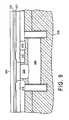
- the wafer portion 200is illustrated after formation of pedestal stack layers that comprise a hi pressure oxide layer 227 , a nitride layer 226 and a thicker oxide layer 225 . These layers will be used to form the pedestal that will be used to define the emitter opening.
- the next step 118is to pattern the pedestal stack to define the pedestal. This can be done by first depositing and patterning photoresist, and then using the patterned photoresist to etch to the thick oxide layer. The photoresist can then be stripped and the nitride layer pattered selective to the patterned thick oxide layer. The hipox layer can then be patterned while leaving the thick oxide layer using a controlled oxide reaction process that will etch selectively remove the hipox layer while leaving the patterned thick oxide. This completes the patterning of the pedestal stack and results in a pedestal stack that comprises thick oxide, nitride and hipox.
- the wafer portion 200is illustrated after the thick oxide 225 has been patterned, and the nitride layer 226 has been patterned selective to the thick oxide.
- FIG. 11the wafer portion 200 is illustrated after the hipox layer 227 has been patterned using the controlled oxide reaction process.
- the next step 120is to form a dopant source layer and a cap layer.
- the dopant source layerwill be used to provide the dopants that form at least a portion of the extrinsic base. In particular, in later processing, the dopants will be diffused from the dopant source layer to form at least an inner extrinsic base portion.
- the dopant source layercan be any suitable layer, such has a doped silicon layer. For example, a layer of between 100 and 200 Angstroms of P++ doped poly or amorphous silicon can be used as the dopant source layer. In this embodiment the dopant source layer can be a selectively grown layer of heavily doped silicon.
- the dopant source layeris grown selectively such that it is formed on the single crystal portions of the SiGe layer and on the amorphous portions of SiGe, but is not formed on the oxide portions of the pedestal. This can be accomplished by stopping the growing process before formation on oxide begins. Standard selective epitaxy techniques known to those skilled in the art may also be used. These methods typically use chlorine based growth chemistries to create a deposition/etch reaction to grow only on silicon exposed areas. The methods are typically employed to create raised source drains FET structures for advanced CMOS devices.
- the cap layeracts as an insulator between the p+ extrinsic base dopant source and the n+ emitter polysilicon which will be deposited on top of the cap layer.
- the cap layerthus helps prevent shorts between the extrinsic base and the emitter. Additionally, the vertical portions of the cap layer will be used to define the emitter opening after the pedestal is removed.
- the cap layercan be any suitable dielectric material. In one embodiment, the cap layer comprises approximately 1000 Angstroms of conformal silicon nitride deposited over the dopant source layer. Turning now to FIG.
- the wafer portionis illustrated after the formation of a dopant source layer 236 where the dopant source layer 236 is a grown single crystal silicon layer doped between 5 ⁇ 10 19 and 1 ⁇ 10 21 atoms/cm 3 , that grows on exposed SiGe surfaces.
- the wafer portionis illustrated after the formation of a cap layer 234 that comprises a nitride layer.
- the next step 122is form a sidewall spacer, and pattern the cap and dopant source layers.
- the sidewall spaceris formed on the sidewalls of the cap where the cap covers the pedestal.
- the sidewall spaceris then used to pattern the underlying dopant sources. These removes the dopant source layer from the outer areas of the transistor, but leaves the dopant source layer where it will be used to form the inner portion of the extrinsic base.
- the dopant source layersmay also be removed outside the spacer during this etch, but need not be.
- the sidewall spacercan be formed from any suitable material that allows it to be used to pattern the underlying cap and dopant source layer.
- the sidewall spacercan be formed with silicon dioxide, allowing it to be used to pattern an underlying nitride cap layer and silicon dopant source layer.
- the sidewall spaceris preferably defined by conformal deposition of the spacer material, followed by a directional etch of the sidewall spacer material. The directional etch removes the material from the horizontal surfaces, while leaving the material on vertical surfaces.
- other suitable methods of forming a sidewall spacercould also be used.
- the underlying cap and dopant source layerscan then patterned using any suitable etch, preferably one that is selective to the sidewall spacer material.
- the spacer widthmay vary between 1000 Angstroms to 8000 Angstroms with a preferred width of 3000 Angstroms. This spacer pushes out the future extrinsic base implant to a distance such that it does not cause implant enhanced diffusion of the intrinsic base.
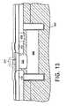
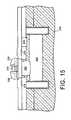
- the wafer portion 200is illustrated after the formation of a sidewall spacer 238 on the cap layer 234 .
- the sidewall spacer 238preferably comprises a material such silicon dioxide that can be used to pattern the underlying cap layer 234 and dopant source layer 236 .
- FIG. 15the wafer portion 200 is shown after the cap layer 234 and the dopant source layer 236 have been patterned using the sidewall spacer 238 as an etch block. This patterning has removed the cap layer 236 and the dopant source layer 236 from the outer regions of the transistor. It has also removed the exposed top portion of the cap layer 236 between the sidewall spacers, exposing the thick oxide portion 225 of the pedestal. Again, it should be noted that it is not required to remove the dopant source layer during this etch.
- the next step 120is to implant the outer portion of the extrinsic base, with the inner portion to be formed later by dopant diffusion.
- the extrinsic base implantwill be partially blocked by remaining sidewall spacers and the pedestal, and thus be formed only in the outer areas of the base.
- the remaining portions of the extrinsic basewill then be formed by diffusion from the dopant source layer.
- This implantwould typically comprise a P+ implant selected to minimize the resistence of the extrinsic base. It should be noted that this implant is not required in many cases.
- the extrinsic baseis to be silicided at the end of the process, or if the implant encroaches too close to the intrinsic base, this implant may be skipped and the transistor optimized without it.
- the conditionswould be very similar to a PFET source/drain implant, namely a Germanium preamorphization implant followed by a high dose/low energy boron dopant implant.
- the wafer portion 200is illustrated after the implantation of the outer portion of the extrinsic base 240 into the polycrystalline portion of the SiGe 224 .
- the outer portion of the extrinsic base 240is formed only in areas not blocked by the sidewall spacer 238 or the pedestal.
- the next step 126is to remove the top portion of the and pedestal and sidewall spacers. This is preferably using a suitable dip out process.
- the sidewall spacers and pedestalcomprise silicon dioxide, they are preferably removed using an isotropic wet etch, such as one containing hydrofluoric acid.
- the removal of the pedestalexposes the nitride portion of the cap.
- FIG. 17the wafer portion 200 is illustrated after the formation the removal of the oxide portion of the pedestal 225 and the sidewall spacers 238 . This removal exposes the nitride portion 226 .
- the next step 128is to deposit spacer material and selectively pattern to form spacers and expose the hipox portion of the pedestal. This is preferably done by depositing a suitable thickness of spacer material, such as 500 Angstroms of silicon nitride. Photoresist is then deposited and patterned to selectively expose the emitter area. The spacer material is then directionally etched. This removes the sidewall spacer material from the horizontal surfaces inside the emitter opening. This additionally can remove the exposed layer from the pedestal stack.
- spacer materialsuch as 500 Angstroms of silicon nitride.
- Photoresistis then deposited and patterned to selectively expose the emitter area.
- the spacer materialis then directionally etched. This removes the sidewall spacer material from the horizontal surfaces inside the emitter opening. This additionally can remove the exposed layer from the pedestal stack.
- the patterned photoresist of this stepto define a pedestal collector implant.
- Thisfacilitates the formation of a pedestal implant that is self aligned to the emitter opening and self aligned with respect to the raised extrinsic base. This enables a reduction in collector base capacitance.
- This implantcan be done before or after the inside nitride spacer etch. Implanting the collector implant to tailor device performance through the emitter opening creates a self-aligned base-collector junction with respect to the emitter-base junction, thus minimizing collector-base capacitance and maximizing F max .
- the wafer portion 200is illustrated after the deposition of spacer material 239 .
- the materialcan comprise 500 Angstroms of silicon nitride.
- FIG. 19the wafer portion is illustrated after the deposition and patterning of photoresist 241 to expose the emitter area, and after the spacer material 239 and nitride pedestal layer 226 has been etched away using a suitable directional etch. This exposes the underlying hipox portion of the pedestal 227 .
- the next step 130is to remove the remaining pedestal to expose the emitter. This can be done using a suitable dip out process.
- the wafer portion 200is illustrated after the photoresist 241 has been stripped and the hipox portion of the pedestal 227 has been removed. This exposes the emitter portion of the single crystal SiGe film 222
- the next step 132is to form the emitter base oxide and deposit and pattern the emitter material.
- the emitter base oxidecan be formed by performing a rapid thermal oxidation of the exposed SiGe The emitter material can then deposited.
- the emitter materialcan be a suitable intrinsic polysilicon that is then doped, or formed from in-situ doped polysilicon, or other suitable material.
- the deposited emitter materialcan then be patterned to leave emitter material only in the emitter region. This is preferably done by depositing and patterning photoresist, and then patterning the emitter material selective to the photoresist and the underlying cap layer.
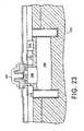
- the wafer portionis illustrated after the formation of the emitter base oxide and the deposition of an emitter material 242 such as doped polysilicon.
- FIG. 22illustrates the wafer portion 200 after the emitter material 242 has been patterned using a suitable photoresist 243 .
- the emitter material 242has been removed except in the emitter areas of the transistor. The etch preferably stops on the remaining spacer layer 239 . After the emitter material has been patterned, the remaining photoresist 243 can be removed.
- the next step 134is to diffuse in the junctions. This is done by performing a suitable annealing process that causes dopants to diffuse from the doped emitter material to form the emitter. Additionally, dopants diffuse from dopant source layer to form at least a portion of the extrinsic base. Because this portion of the extrinsic base is formed by diffusing dopants, it avoids the damage to the device that would be caused by implanting the extrinsic base. This reduced damage enhances dopant diffusion into the intrinsic base. Additionally, the formed extrinsic base can have improved resistence, resulting in an improved maximum frequency for the bipolar device.
- the remaining portions of the dopant source layerremain and form a raised portion of the extrinsic base that has improved resistence and provides for the majority of current flow through the extrinsic base. Because the raised extrinsic base is built above the intrinsic base, the collector-base junction capacitance will be reduced over that of a conventional NPN, thus resulting in higher F max . In an implant extrinsic base, three is less control over the depth of the extrinsic base implant and it is deeper, which results in higher base-collector capacitance and lower F max .
- FIG. 24a second method 800 for forming an integrated circuit in accordance is illustrated. This method is essentially identical to the first except that it does not use the selective deposition of the raised extrinsic base as the first preferred embodiment.
- Steps 801 through 814 of method 800track parallel steps 101 through 114 in method 100 .
- the next step 816is to form a pedestal, deposit a dopant source layer and a cap layer.
- the pedestalwill be used to define the emitter opening, and in this method is formed by depositing a dielectric such as silicon dioxide and then patterning the oxide to form the pedestal in the location where the emitter is to be formed.
- a dopant source layeris deposited over the wafer. Again, the dopant source layer will be used to provide the dopants that form at least a portion of the extrinsic base. In particular, in later processing, the dopants will be diffused from the dopant source layer to form at least an inner extrinsic base portion.
- the dopant source layercan be any suitable layer, such has a doped silicon layer.
- a layer of between 100 and 200 Angstroms of P++ doped poly or amorphous siliconcan be used as the dopant source layer.
- the material used heremay be nonselective and thus is deposited over the pedestal, in contrast to the previous process that used selective deposition of the diffusion source.
- the cap layeracts as an insulator between the p+ extrinsic base dopant source and the n+ emitter polysilicon which will be deposited on top of the cap layer.
- the cap layerthus helps prevent shorts between the extrinsic base and the emitter. Additionally, the vertical portions of the cap layer will be used to define the emitter opening after the pedestal is removed.
- the cap layercan be any suitable dielectric material. In one embodiment, the cap layer comprises approximately 1000 Angstroms of conformal silicon nitride deposited over the dopant source layer. Turning now to FIG.
- the wafer portionis illustrated after the completion of steps 801 to 814 and the formation of a pedestal 832 by depositing and patterning a suitable oxide layer, and the formation of a of a dopant source layer 836 and a cap layer 834 over the pedestal 832 .
- the sidewall spacercan be formed with silicon dioxide, allowing it to be used to pattern an underlying nitride cap layer and silicon dopant source layer.
- the sidewall spaceris preferably defined by conformal deposition of the spacer material, followed by a directional etch of the sidewall spacer material. The directional etch removes the material from the horizontal surfaces, while leaving the material on vertical surfaces.
- other suitable methods of forming a sidewall spacercould also be used.
- the underlying cap and dopant source layerscan then patterned using any suitable etch, preferably one that is selective to the sidewall spacer material.
- the spacer widthmay vary between 1000 Angstroms to 8000 Angstroms with a preferred width of 2000 Angstroms. This spacer pushes out the future extrinsic base implant to a distance such that it does not cause implant enhanced diffusion of the intrinsic base.
- the wafer portion 200is illustrated after the formation of a sidewall spacer 838 on the cap layer 834 .
- the sidewall spacer 838preferably comprises a material such silicon dioxide that can be used to pattern the underlying cap layer 834 and dopant source layer 836 .
- FIG. 27the wafer portion 200 is shown after the cap layer 834 and the dopant source layer 836 have been patterned using the sidewall spacer 838 as an etch block. This patterning has removed the cap layer 836 and the dopant source layer 836 from the outer regions of the transistor. Again, it should be noted that it is not required to remove the dopant source layer during this etch. Additionally, the cap layer 836 has been removed from the emitter area, exposing pedestal 832 .
- the next step 820is to implant the extrinsic base. Specifically, to implant the outer portion of the extrinsic base, with the inner portion to be formed later by dopant diffusion.
- the extrinsic base implantwould be partially blocked remaining sidewall spacers and pedestal, and thus be formed only in the outer areas of the base. The remaining portions of the extrinsic base will then be formed by diffusion from the dopant source layer.
- This implantwould typically comprise a P+ implant selected to minimize the resistence of the extrinsic base.
- This extrinsic base implantwould be similar to that described in the first embodiment. It would be a shallow, high dose p type implant very similar to that used in a standard PFET CMOS source/drain.
- the wafer portion 200is illustrated after the implantation of the outer portion of the extrinsic base 240 into the polycrystalline portion of the SiGe 224 .
- the outer portion of the extrinsic base 240is formed only in areas not blocked by the sidewall spacer 838 or the pedestal 832 .
- the next step 822is to remove the pedestal and sidewall spacers. This is preferably accomplished using a suitable dip out process.
- the sidewall spacers and pedestalcomprise silicon dioxide, they are preferably removed using an isotropic wet etch, such as one containing hydrofluoric acid.
- the removal of the pedestalexposes the underlying SiGe, exposing the portion where the intrinsic base will later be formed. It also exposes a portion of the dopant source layer.
- FIG. 29the wafer portion 200 is illustrated after the formation the removal of the pedestal 832 and the sidewall spacers 838 . This removal exposes the cap layer 834 , and a portion of the dopant source layer 836 . It also exposes a portion of the SiGe layer 222 .
- the next step 824is to remove the exposed portion of the dopant source layer, which lines the vertical part of the cap.
- the dopant source layer sandwiched horizontally between the cap and the SiGe epiwill remain.
- the dopant source layercan be removed using any suitable process which removes or renders inactive the dopant layer.
- the removalcan comprise a high pressure oxidation process that converts the exposed doped polysilicon to silicon dioxide.
- the wafer portion 200is illustrated after the exposed portion of the dopant source layer 836 has been removed by converting the exposed dopant source layer to a layer silicon dioxide 845 . Again, this conversion can be accomplished using a suitable high pressure oxidation process.
- the next step 828is to deposit spacer material and selectively pattern to form spacers and expose the converted dopant source layer. This is preferably done by depositing a suitable thickness of spacer material, such as 500 Angstroms of silicon nitride. Photoresist is then deposited and patterned to selectively expose the emitter area. The spacer material is then directionally etched. This removes the sidewall spacer material from the horizontal surfaces and forms sidewall spacers over the converted dopant source layer.
- a suitable thickness of spacer materialsuch as 500 Angstroms of silicon nitride.
- Photoresistis then deposited and patterned to selectively expose the emitter area.
- the spacer materialis then directionally etched. This removes the sidewall spacer material from the horizontal surfaces and forms sidewall spacers over the converted dopant source layer.
- the wafer portion 200is illustrated after the deposition of spacer material 847 .
- the materialcan comprise 500 Angstroms of silicon nitride.
- FIG. 32the wafer portion is illustrated after the deposition and patterning of photoresist 849 to expose the emitter area, and after the spacer material 847 etched away using a suitable directional etch, forming sidewall spacers over the sides of hipox 845 while exposing the lower portion of hipox 845 .
- the next step 830is to form the emitter opening.
- the emitter openingis formed by etching through the silicon dioxide to the SiGe layer. This etch can be performed selective to the sidewall spacers formed on the vertical portions of the cap layer and the converted dopant source layer.
- the wafer portion 200is illustrated after the bottom portion of converted dopant source layer, the hipox 245 has been etched away selective to sidewall spacers. This etch exposes the emitter portion of the single crystal SiGe film 222 .
- Steps 832 to 836then parallel steps 132 to 136 of method 100 .
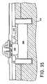
- FIG. 34illustrate an example of the formation and patterning of emitter material 255 .
- FIG. 35illustrates after the diffusion of dopants from the emitter material 255 and dopant source layer 836 to form the emitter 860 and the outer portion of the extrinsic base 862 .
- the present inventionthus provides a unique device structure and method that provides increased transistor performance in integrated bipolar circuit devices.
- the preferred embodiment of the present inventionprovides improved high speed performance by providing reduced base resistence.
- the preferred designforms the extrinsic base by diffusing dopants from a dopant source layer and into the extrinsic base region. This diffusion of dopants forms at least a portion of the extrinsic base. In particular, the portion adjacent to the intrinsic base region is formed by diffusion.
- This solutionavoids the problems caused by traditional solutions that implanted the extrinsic base. Specifically, by forming at least a portion of the extrinsic base by diffusion, the problem of damage to base region is minimized. This reduced damage enhances dopant diffusion into the intrinsic base. Additionally, the formed extrinsic base can have improved resistence, resulting in an improved maximum frequency for the bipolar device.
Landscapes
- Bipolar Transistors (AREA)
Abstract
Description
Claims (17)
Priority Applications (1)
| Application Number | Priority Date | Filing Date | Title |
|---|---|---|---|
| US10/865,138US6900519B2 (en) | 2002-07-18 | 2004-06-10 | Diffused extrinsic base and method for fabrication |
Applications Claiming Priority (2)
| Application Number | Priority Date | Filing Date | Title |
|---|---|---|---|
| US10/064,476US6869854B2 (en) | 2002-07-18 | 2002-07-18 | Diffused extrinsic base and method for fabrication |
| US10/865,138US6900519B2 (en) | 2002-07-18 | 2004-06-10 | Diffused extrinsic base and method for fabrication |
Related Parent Applications (1)
| Application Number | Title | Priority Date | Filing Date |
|---|---|---|---|
| US10/064,476DivisionUS6869854B2 (en) | 2002-07-18 | 2002-07-18 | Diffused extrinsic base and method for fabrication |
Publications (2)
| Publication Number | Publication Date |
|---|---|
| US20040222495A1 US20040222495A1 (en) | 2004-11-11 |
| US6900519B2true US6900519B2 (en) | 2005-05-31 |
Family
ID=30442202
Family Applications (2)
| Application Number | Title | Priority Date | Filing Date |
|---|---|---|---|
| US10/064,476Expired - Fee RelatedUS6869854B2 (en) | 2002-07-18 | 2002-07-18 | Diffused extrinsic base and method for fabrication |
| US10/865,138Expired - LifetimeUS6900519B2 (en) | 2002-07-18 | 2004-06-10 | Diffused extrinsic base and method for fabrication |
Family Applications Before (1)
| Application Number | Title | Priority Date | Filing Date |
|---|---|---|---|
| US10/064,476Expired - Fee RelatedUS6869854B2 (en) | 2002-07-18 | 2002-07-18 | Diffused extrinsic base and method for fabrication |
Country Status (1)
| Country | Link |
|---|---|
| US (2) | US6869854B2 (en) |
Cited By (46)
| Publication number | Priority date | Publication date | Assignee | Title |
|---|---|---|---|---|
| US8404551B2 (en) | 2010-12-03 | 2013-03-26 | Suvolta, Inc. | Source/drain extension control for advanced transistors |
| US8421162B2 (en) | 2009-09-30 | 2013-04-16 | Suvolta, Inc. | Advanced transistors with punch through suppression |
| US8461875B1 (en) | 2011-02-18 | 2013-06-11 | Suvolta, Inc. | Digital circuits having improved transistors, and methods therefor |
| US8525271B2 (en) | 2011-03-03 | 2013-09-03 | Suvolta, Inc. | Semiconductor structure with improved channel stack and method for fabrication thereof |
| US8530286B2 (en) | 2010-04-12 | 2013-09-10 | Suvolta, Inc. | Low power semiconductor transistor structure and method of fabrication thereof |
| US8569128B2 (en) | 2010-06-21 | 2013-10-29 | Suvolta, Inc. | Semiconductor structure and method of fabrication thereof with mixed metal types |
| US8569156B1 (en) | 2011-05-16 | 2013-10-29 | Suvolta, Inc. | Reducing or eliminating pre-amorphization in transistor manufacture |
| US8599623B1 (en) | 2011-12-23 | 2013-12-03 | Suvolta, Inc. | Circuits and methods for measuring circuit elements in an integrated circuit device |
| US8614128B1 (en) | 2011-08-23 | 2013-12-24 | Suvolta, Inc. | CMOS structures and processes based on selective thinning |
| US8629016B1 (en) | 2011-07-26 | 2014-01-14 | Suvolta, Inc. | Multiple transistor types formed in a common epitaxial layer by differential out-diffusion from a doped underlayer |
| US8637955B1 (en) | 2012-08-31 | 2014-01-28 | Suvolta, Inc. | Semiconductor structure with reduced junction leakage and method of fabrication thereof |
| US8645878B1 (en) | 2011-08-23 | 2014-02-04 | Suvolta, Inc. | Porting a circuit design from a first semiconductor process to a second semiconductor process |
| US8713511B1 (en) | 2011-09-16 | 2014-04-29 | Suvolta, Inc. | Tools and methods for yield-aware semiconductor manufacturing process target generation |
| US8735987B1 (en) | 2011-06-06 | 2014-05-27 | Suvolta, Inc. | CMOS gate stack structures and processes |
| US8748270B1 (en) | 2011-03-30 | 2014-06-10 | Suvolta, Inc. | Process for manufacturing an improved analog transistor |
| US8748986B1 (en) | 2011-08-05 | 2014-06-10 | Suvolta, Inc. | Electronic device with controlled threshold voltage |
| US8759872B2 (en) | 2010-06-22 | 2014-06-24 | Suvolta, Inc. | Transistor with threshold voltage set notch and method of fabrication thereof |
| US8796048B1 (en) | 2011-05-11 | 2014-08-05 | Suvolta, Inc. | Monitoring and measurement of thin film layers |
| US8811068B1 (en) | 2011-05-13 | 2014-08-19 | Suvolta, Inc. | Integrated circuit devices and methods |
| US8819603B1 (en) | 2011-12-15 | 2014-08-26 | Suvolta, Inc. | Memory circuits and methods of making and designing the same |
| US8816754B1 (en) | 2012-11-02 | 2014-08-26 | Suvolta, Inc. | Body bias circuits and methods |
| US8863064B1 (en) | 2012-03-23 | 2014-10-14 | Suvolta, Inc. | SRAM cell layout structure and devices therefrom |
| US8877619B1 (en) | 2012-01-23 | 2014-11-04 | Suvolta, Inc. | Process for manufacture of integrated circuits with different channel doping transistor architectures and devices therefrom |
| US8883600B1 (en) | 2011-12-22 | 2014-11-11 | Suvolta, Inc. | Transistor having reduced junction leakage and methods of forming thereof |
| US8895327B1 (en) | 2011-12-09 | 2014-11-25 | Suvolta, Inc. | Tipless transistors, short-tip transistors, and methods and circuits therefor |
| US8970289B1 (en) | 2012-01-23 | 2015-03-03 | Suvolta, Inc. | Circuits and devices for generating bi-directional body bias voltages, and methods therefor |
| US8995204B2 (en) | 2011-06-23 | 2015-03-31 | Suvolta, Inc. | Circuit devices and methods having adjustable transistor body bias |
| US8999861B1 (en) | 2011-05-11 | 2015-04-07 | Suvolta, Inc. | Semiconductor structure with substitutional boron and method for fabrication thereof |
| US9041126B2 (en) | 2012-09-21 | 2015-05-26 | Mie Fujitsu Semiconductor Limited | Deeply depleted MOS transistors having a screening layer and methods thereof |
| US9054219B1 (en) | 2011-08-05 | 2015-06-09 | Mie Fujitsu Semiconductor Limited | Semiconductor devices having fin structures and fabrication methods thereof |
| US9070477B1 (en) | 2012-12-12 | 2015-06-30 | Mie Fujitsu Semiconductor Limited | Bit interleaved low voltage static random access memory (SRAM) and related methods |
| US9093550B1 (en) | 2012-01-31 | 2015-07-28 | Mie Fujitsu Semiconductor Limited | Integrated circuits having a plurality of high-K metal gate FETs with various combinations of channel foundation structure and gate stack structure and methods of making same |
| US9093997B1 (en) | 2012-11-15 | 2015-07-28 | Mie Fujitsu Semiconductor Limited | Slew based process and bias monitors and related methods |
| US9112484B1 (en) | 2012-12-20 | 2015-08-18 | Mie Fujitsu Semiconductor Limited | Integrated circuit process and bias monitors and related methods |
| US9112057B1 (en) | 2012-09-18 | 2015-08-18 | Mie Fujitsu Semiconductor Limited | Semiconductor devices with dopant migration suppression and method of fabrication thereof |
| US9236466B1 (en) | 2011-10-07 | 2016-01-12 | Mie Fujitsu Semiconductor Limited | Analog circuits having improved insulated gate transistors, and methods therefor |
| US9268885B1 (en) | 2013-02-28 | 2016-02-23 | Mie Fujitsu Semiconductor Limited | Integrated circuit device methods and models with predicted device metric variations |
| US9299801B1 (en) | 2013-03-14 | 2016-03-29 | Mie Fujitsu Semiconductor Limited | Method for fabricating a transistor device with a tuned dopant profile |
| US9299698B2 (en) | 2012-06-27 | 2016-03-29 | Mie Fujitsu Semiconductor Limited | Semiconductor structure with multiple transistors having various threshold voltages |
| US9319013B2 (en) | 2014-08-19 | 2016-04-19 | Mie Fujitsu Semiconductor Limited | Operational amplifier input offset correction with transistor threshold voltage adjustment |
| US9406567B1 (en) | 2012-02-28 | 2016-08-02 | Mie Fujitsu Semiconductor Limited | Method for fabricating multiple transistor devices on a substrate with varying threshold voltages |
| US9431068B2 (en) | 2012-10-31 | 2016-08-30 | Mie Fujitsu Semiconductor Limited | Dynamic random access memory (DRAM) with low variation transistor peripheral circuits |
| US9478571B1 (en) | 2013-05-24 | 2016-10-25 | Mie Fujitsu Semiconductor Limited | Buried channel deeply depleted channel transistor |
| US9608096B1 (en) | 2015-10-02 | 2017-03-28 | Globalfoundries Inc. | Implementing stress in a bipolar junction transistor |
| US9710006B2 (en) | 2014-07-25 | 2017-07-18 | Mie Fujitsu Semiconductor Limited | Power up body bias circuits and methods |
| US10074568B2 (en) | 2009-09-30 | 2018-09-11 | Mie Fujitsu Semiconductor Limited | Electronic devices and systems, and methods for making and using same |
Families Citing this family (15)
| Publication number | Priority date | Publication date | Assignee | Title |
|---|---|---|---|---|
| US6900091B2 (en)* | 2002-08-14 | 2005-05-31 | Advanced Analogic Technologies, Inc. | Isolated complementary MOS devices in epi-less substrate |
| US7075126B2 (en)* | 2004-02-27 | 2006-07-11 | International Business Machines Corporation | Transistor structure with minimized parasitics and method of fabricating the same |
| DE102004021241A1 (en) | 2004-04-30 | 2005-11-17 | Infineon Technologies Ag | A method of fabricating a planar spacer, an associated bipolar transistor, and associated BiCMOS circuitry |
| US7265018B2 (en)* | 2004-09-21 | 2007-09-04 | International Business Machines Corporation | Method to build self-aligned NPN in advanced BiCMOS technology |
| DE102004053394B4 (en)* | 2004-11-05 | 2010-08-19 | Atmel Automotive Gmbh | Semiconductor arrangement and method for producing a semiconductor device |
| DE102004053393B4 (en)* | 2004-11-05 | 2007-01-11 | Atmel Germany Gmbh | Method for producing a vertically integrated cascode structure and vertically integrated cascode structure |
| US7491614B2 (en)* | 2005-01-13 | 2009-02-17 | International Business Machines Corporation | Methods for forming channel stop for deep trench isolation prior to deep trench etch |
| US7329940B2 (en)* | 2005-11-02 | 2008-02-12 | International Business Machines Corporation | Semiconductor structure and method of manufacture |
| US7892910B2 (en)* | 2007-02-28 | 2011-02-22 | International Business Machines Corporation | Bipolar transistor with raised extrinsic self-aligned base using selective epitaxial growth for BiCMOS integration |
| US8409959B2 (en) | 2007-03-13 | 2013-04-02 | Micron Technology, Inc. | Vertically base-connected bipolar transistor |
| US7999250B2 (en)* | 2008-03-04 | 2011-08-16 | Hvvi Semiconductors, Inc. | Silicon-germanium-carbon semiconductor structure |
| CN102097464B (en)* | 2009-12-15 | 2012-10-03 | 上海华虹Nec电子有限公司 | High-voltage bipolar transistor |
| DE102014113989B4 (en) | 2014-09-26 | 2020-06-04 | Infineon Technologies Ag | Method of manufacturing a bipolar transistor |
| US20160269021A1 (en)* | 2015-02-06 | 2016-09-15 | Ideal Power Inc. | Collector-Side-Base-Driven Two-Base-Contact Bipolar Transistor with Reduced Series Resistance |
| JP6542610B2 (en)* | 2015-08-20 | 2019-07-10 | ルネサスエレクトロニクス株式会社 | Semiconductor device manufacturing method |
Citations (14)
| Publication number | Priority date | Publication date | Assignee | Title |
|---|---|---|---|---|
| US3904450A (en) | 1974-04-26 | 1975-09-09 | Bell Telephone Labor Inc | Method of fabricating injection logic integrated circuits using oxide isolation |
| US4252581A (en) | 1979-10-01 | 1981-02-24 | International Business Machines Corporation | Selective epitaxy method for making filamentary pedestal transistor |
| EP0100664A2 (en) | 1982-07-30 | 1984-02-15 | Corning Glass Works | Specimen cup and cap assembly for clinical analyzer |
| US4495512A (en) | 1982-06-07 | 1985-01-22 | International Business Machines Corporation | Self-aligned bipolar transistor with inverted polycide base contact |
| US4860085A (en) | 1986-06-06 | 1989-08-22 | American Telephone And Telegraph Company, At&T Bell Laboratories | Submicron bipolar transistor with buried silicide region |
| US5117271A (en) | 1990-12-07 | 1992-05-26 | International Business Machines Corporation | Low capacitance bipolar junction transistor and fabrication process therfor |
| US5213989A (en)* | 1992-06-24 | 1993-05-25 | Motorola, Inc. | Method for forming a grown bipolar electrode contact using a sidewall seed |
| US5268314A (en) | 1990-01-16 | 1993-12-07 | Philips Electronics North America Corp. | Method of forming a self-aligned bipolar transistor |
| US5439833A (en) | 1994-03-15 | 1995-08-08 | National Semiconductor Corp. | Method of making truly complementary and self-aligned bipolar and CMOS transistor structures with minimized base and gate resistances and parasitic capacitance |
| US5593905A (en) | 1995-02-23 | 1997-01-14 | Texas Instruments Incorporated | Method of forming stacked barrier-diffusion source and etch stop for double polysilicon BJT with patterned base link |
| US5629556A (en) | 1995-01-09 | 1997-05-13 | Texas Instruments Incorporated | High speed bipolar transistor using a patterned etch stop and diffusion source |
| US5761080A (en) | 1995-11-22 | 1998-06-02 | International Business Machines Corporation | Method and apparatus for modeling capacitance in an integrated circuit |
| WO1999052138A1 (en) | 1998-04-08 | 1999-10-14 | Aeroflex Utmc Microelectronic Systems Inc. | A bipolar transistor having low extrinsic base resistance |
| US6437376B1 (en)* | 2000-03-01 | 2002-08-20 | Applied Micro Circuits Corporation | Heterojunction bipolar transistor (HBT) with three-dimensional base contact |
Family Cites Families (3)
| Publication number | Priority date | Publication date | Assignee | Title |
|---|---|---|---|---|
| US5592017A (en)* | 1995-03-23 | 1997-01-07 | Texas Instruments Incorporated | Self-aligned double poly BJT using sige spacers as extrinsic base contacts |
| JP3186691B2 (en)* | 1998-04-07 | 2001-07-11 | 日本電気株式会社 | Semiconductor device and method for forming the same |
| US6177325B1 (en)* | 1998-05-18 | 2001-01-23 | Winbond Electronics Corp. | Self-aligned emitter and base BJT process and structure |
- 2002
- 2002-07-18USUS10/064,476patent/US6869854B2/ennot_activeExpired - Fee Related
- 2004
- 2004-06-10USUS10/865,138patent/US6900519B2/ennot_activeExpired - Lifetime
Patent Citations (14)
| Publication number | Priority date | Publication date | Assignee | Title |
|---|---|---|---|---|
| US3904450A (en) | 1974-04-26 | 1975-09-09 | Bell Telephone Labor Inc | Method of fabricating injection logic integrated circuits using oxide isolation |
| US4252581A (en) | 1979-10-01 | 1981-02-24 | International Business Machines Corporation | Selective epitaxy method for making filamentary pedestal transistor |
| US4495512A (en) | 1982-06-07 | 1985-01-22 | International Business Machines Corporation | Self-aligned bipolar transistor with inverted polycide base contact |
| EP0100664A2 (en) | 1982-07-30 | 1984-02-15 | Corning Glass Works | Specimen cup and cap assembly for clinical analyzer |
| US4860085A (en) | 1986-06-06 | 1989-08-22 | American Telephone And Telegraph Company, At&T Bell Laboratories | Submicron bipolar transistor with buried silicide region |
| US5268314A (en) | 1990-01-16 | 1993-12-07 | Philips Electronics North America Corp. | Method of forming a self-aligned bipolar transistor |
| US5117271A (en) | 1990-12-07 | 1992-05-26 | International Business Machines Corporation | Low capacitance bipolar junction transistor and fabrication process therfor |
| US5213989A (en)* | 1992-06-24 | 1993-05-25 | Motorola, Inc. | Method for forming a grown bipolar electrode contact using a sidewall seed |
| US5439833A (en) | 1994-03-15 | 1995-08-08 | National Semiconductor Corp. | Method of making truly complementary and self-aligned bipolar and CMOS transistor structures with minimized base and gate resistances and parasitic capacitance |
| US5629556A (en) | 1995-01-09 | 1997-05-13 | Texas Instruments Incorporated | High speed bipolar transistor using a patterned etch stop and diffusion source |
| US5593905A (en) | 1995-02-23 | 1997-01-14 | Texas Instruments Incorporated | Method of forming stacked barrier-diffusion source and etch stop for double polysilicon BJT with patterned base link |
| US5761080A (en) | 1995-11-22 | 1998-06-02 | International Business Machines Corporation | Method and apparatus for modeling capacitance in an integrated circuit |
| WO1999052138A1 (en) | 1998-04-08 | 1999-10-14 | Aeroflex Utmc Microelectronic Systems Inc. | A bipolar transistor having low extrinsic base resistance |
| US6437376B1 (en)* | 2000-03-01 | 2002-08-20 | Applied Micro Circuits Corporation | Heterojunction bipolar transistor (HBT) with three-dimensional base contact |
Non-Patent Citations (3)
| Title |
|---|
| IBM Technical Disclosure Bulletin, vol. 24, No. 7A, Dec. 1981, "Polycide Bipolar Transistor Process", F. Barson, et al., pp. 3424-3426. |
| IBM Technical Disclosure Bulletin, vol. 25, No. 4, Sep. 1982, "Using a Doubly Implanted Polysilicon Layer for Forming Base and Emitter Regions", C.G. Jambotkar, ppp. 1887-1889. |
| IBM Technical Disclosure Bulletin, vol. 26, No. 2, Jul. 1983, "Transistor Collector Doping for Reduced Capacitance", W.P. Dumke, p. 492. |
Cited By (95)
| Publication number | Priority date | Publication date | Assignee | Title |
|---|---|---|---|---|
| US10325986B2 (en) | 2009-09-30 | 2019-06-18 | Mie Fujitsu Semiconductor Limited | Advanced transistors with punch through suppression |
| US8421162B2 (en) | 2009-09-30 | 2013-04-16 | Suvolta, Inc. | Advanced transistors with punch through suppression |
| US10074568B2 (en) | 2009-09-30 | 2018-09-11 | Mie Fujitsu Semiconductor Limited | Electronic devices and systems, and methods for making and using same |
| US9263523B2 (en) | 2009-09-30 | 2016-02-16 | Mie Fujitsu Semiconductor Limited | Advanced transistors with punch through suppression |
| US9508800B2 (en) | 2009-09-30 | 2016-11-29 | Mie Fujitsu Semiconductor Limited | Advanced transistors with punch through suppression |
| US11062950B2 (en) | 2009-09-30 | 2021-07-13 | United Semiconductor Japan Co., Ltd. | Electronic devices and systems, and methods for making and using the same |
| US10224244B2 (en) | 2009-09-30 | 2019-03-05 | Mie Fujitsu Semiconductor Limited | Electronic devices and systems, and methods for making and using the same |
| US10217668B2 (en) | 2009-09-30 | 2019-02-26 | Mie Fujitsu Semiconductor Limited | Electronic devices and systems, and methods for making and using the same |
| US11887895B2 (en) | 2009-09-30 | 2024-01-30 | United Semiconductor Japan Co., Ltd. | Electronic devices and systems, and methods for making and using the same |
| US9496261B2 (en) | 2010-04-12 | 2016-11-15 | Mie Fujitsu Semiconductor Limited | Low power semiconductor transistor structure and method of fabrication thereof |
| US9865596B2 (en) | 2010-04-12 | 2018-01-09 | Mie Fujitsu Semiconductor Limited | Low power semiconductor transistor structure and method of fabrication thereof |
| US8530286B2 (en) | 2010-04-12 | 2013-09-10 | Suvolta, Inc. | Low power semiconductor transistor structure and method of fabrication thereof |
| US8569128B2 (en) | 2010-06-21 | 2013-10-29 | Suvolta, Inc. | Semiconductor structure and method of fabrication thereof with mixed metal types |
| US9224733B2 (en) | 2010-06-21 | 2015-12-29 | Mie Fujitsu Semiconductor Limited | Semiconductor structure and method of fabrication thereof with mixed metal types |
| US9418987B2 (en) | 2010-06-22 | 2016-08-16 | Mie Fujitsu Semiconductor Limited | Transistor with threshold voltage set notch and method of fabrication thereof |
| US9922977B2 (en) | 2010-06-22 | 2018-03-20 | Mie Fujitsu Semiconductor Limited | Transistor with threshold voltage set notch and method of fabrication thereof |
| US8759872B2 (en) | 2010-06-22 | 2014-06-24 | Suvolta, Inc. | Transistor with threshold voltage set notch and method of fabrication thereof |
| US8563384B2 (en) | 2010-12-03 | 2013-10-22 | Suvolta, Inc. | Source/drain extension control for advanced transistors |
| US8686511B2 (en) | 2010-12-03 | 2014-04-01 | Suvolta, Inc. | Source/drain extension control for advanced transistors |
| US9006843B2 (en) | 2010-12-03 | 2015-04-14 | Suvolta, Inc. | Source/drain extension control for advanced transistors |
| US8404551B2 (en) | 2010-12-03 | 2013-03-26 | Suvolta, Inc. | Source/drain extension control for advanced transistors |
| US10250257B2 (en) | 2011-02-18 | 2019-04-02 | Mie Fujitsu Semiconductor Limited | Digital circuits having improved transistors, and methods therefor |
| US9838012B2 (en) | 2011-02-18 | 2017-12-05 | Mie Fujitsu Semiconductor Limited | Digital circuits having improved transistors, and methods therefor |
| US9985631B2 (en) | 2011-02-18 | 2018-05-29 | Mie Fujitsu Semiconductor Limited | Digital circuits having improved transistors, and methods therefor |
| US9184750B1 (en) | 2011-02-18 | 2015-11-10 | Mie Fujitsu Semiconductor Limited | Digital circuits having improved transistors, and methods therefor |
| US9680470B2 (en) | 2011-02-18 | 2017-06-13 | Mie Fujitsu Semiconductor Limited | Digital circuits having improved transistors, and methods therefor |
| US8461875B1 (en) | 2011-02-18 | 2013-06-11 | Suvolta, Inc. | Digital circuits having improved transistors, and methods therefor |
| US9111785B2 (en) | 2011-03-03 | 2015-08-18 | Mie Fujitsu Semiconductor Limited | Semiconductor structure with improved channel stack and method for fabrication thereof |
| US8525271B2 (en) | 2011-03-03 | 2013-09-03 | Suvolta, Inc. | Semiconductor structure with improved channel stack and method for fabrication thereof |
| US9093469B2 (en) | 2011-03-30 | 2015-07-28 | Mie Fujitsu Semiconductor Limited | Analog transistor |
| US8748270B1 (en) | 2011-03-30 | 2014-06-10 | Suvolta, Inc. | Process for manufacturing an improved analog transistor |
| US8796048B1 (en) | 2011-05-11 | 2014-08-05 | Suvolta, Inc. | Monitoring and measurement of thin film layers |
| US8999861B1 (en) | 2011-05-11 | 2015-04-07 | Suvolta, Inc. | Semiconductor structure with substitutional boron and method for fabrication thereof |
| US8811068B1 (en) | 2011-05-13 | 2014-08-19 | Suvolta, Inc. | Integrated circuit devices and methods |
| US9741428B2 (en) | 2011-05-13 | 2017-08-22 | Mie Fujitsu Semiconductor Limited | Integrated circuit devices and methods |
| US9966130B2 (en) | 2011-05-13 | 2018-05-08 | Mie Fujitsu Semiconductor Limited | Integrated circuit devices and methods |
| US9362291B1 (en) | 2011-05-13 | 2016-06-07 | Mie Fujitsu Semiconductor Limited | Integrated circuit devices and methods |
| US8937005B2 (en) | 2011-05-16 | 2015-01-20 | Suvolta, Inc. | Reducing or eliminating pre-amorphization in transistor manufacture |
| US9514940B2 (en) | 2011-05-16 | 2016-12-06 | Mie Fujitsu Semiconductor Limited | Reducing or eliminating pre-amorphization in transistor manufacture |
| US9793172B2 (en) | 2011-05-16 | 2017-10-17 | Mie Fujitsu Semiconductor Limited | Reducing or eliminating pre-amorphization in transistor manufacture |
| US8569156B1 (en) | 2011-05-16 | 2013-10-29 | Suvolta, Inc. | Reducing or eliminating pre-amorphization in transistor manufacture |
| US8735987B1 (en) | 2011-06-06 | 2014-05-27 | Suvolta, Inc. | CMOS gate stack structures and processes |
| US9281248B1 (en) | 2011-06-06 | 2016-03-08 | Mie Fujitsu Semiconductor Limited | CMOS gate stack structures and processes |
| US8995204B2 (en) | 2011-06-23 | 2015-03-31 | Suvolta, Inc. | Circuit devices and methods having adjustable transistor body bias |
| US8653604B1 (en) | 2011-07-26 | 2014-02-18 | Suvolta, Inc. | Multiple transistor types formed in a common epitaxial layer by differential out-diffusion from a doped underlayer |
| US8629016B1 (en) | 2011-07-26 | 2014-01-14 | Suvolta, Inc. | Multiple transistor types formed in a common epitaxial layer by differential out-diffusion from a doped underlayer |
| US8916937B1 (en) | 2011-07-26 | 2014-12-23 | Suvolta, Inc. | Multiple transistor types formed in a common epitaxial layer by differential out-diffusion from a doped underlayer |
| US8748986B1 (en) | 2011-08-05 | 2014-06-10 | Suvolta, Inc. | Electronic device with controlled threshold voltage |
| US8963249B1 (en) | 2011-08-05 | 2015-02-24 | Suvolta, Inc. | Electronic device with controlled threshold voltage |
| US9054219B1 (en) | 2011-08-05 | 2015-06-09 | Mie Fujitsu Semiconductor Limited | Semiconductor devices having fin structures and fabrication methods thereof |
| US8645878B1 (en) | 2011-08-23 | 2014-02-04 | Suvolta, Inc. | Porting a circuit design from a first semiconductor process to a second semiconductor process |
| US8806395B1 (en) | 2011-08-23 | 2014-08-12 | Suvolta, Inc. | Porting a circuit design from a first semiconductor process to a second semiconductor process |
| US9117746B1 (en) | 2011-08-23 | 2015-08-25 | Mie Fujitsu Semiconductor Limited | Porting a circuit design from a first semiconductor process to a second semiconductor process |
| US8614128B1 (en) | 2011-08-23 | 2013-12-24 | Suvolta, Inc. | CMOS structures and processes based on selective thinning |
| US9391076B1 (en) | 2011-08-23 | 2016-07-12 | Mie Fujitsu Semiconductor Limited | CMOS structures and processes based on selective thinning |
| US8713511B1 (en) | 2011-09-16 | 2014-04-29 | Suvolta, Inc. | Tools and methods for yield-aware semiconductor manufacturing process target generation |
| US9236466B1 (en) | 2011-10-07 | 2016-01-12 | Mie Fujitsu Semiconductor Limited | Analog circuits having improved insulated gate transistors, and methods therefor |
| US8895327B1 (en) | 2011-12-09 | 2014-11-25 | Suvolta, Inc. | Tipless transistors, short-tip transistors, and methods and circuits therefor |
| US8819603B1 (en) | 2011-12-15 | 2014-08-26 | Suvolta, Inc. | Memory circuits and methods of making and designing the same |
| US8883600B1 (en) | 2011-12-22 | 2014-11-11 | Suvolta, Inc. | Transistor having reduced junction leakage and methods of forming thereof |
| US9368624B2 (en) | 2011-12-22 | 2016-06-14 | Mie Fujitsu Semiconductor Limited | Method for fabricating a transistor with reduced junction leakage current |
| US9196727B2 (en) | 2011-12-22 | 2015-11-24 | Mie Fujitsu Semiconductor Limited | High uniformity screen and epitaxial layers for CMOS devices |
| US8599623B1 (en) | 2011-12-23 | 2013-12-03 | Suvolta, Inc. | Circuits and methods for measuring circuit elements in an integrated circuit device |
| US8877619B1 (en) | 2012-01-23 | 2014-11-04 | Suvolta, Inc. | Process for manufacture of integrated circuits with different channel doping transistor architectures and devices therefrom |
| US8970289B1 (en) | 2012-01-23 | 2015-03-03 | Suvolta, Inc. | Circuits and devices for generating bi-directional body bias voltages, and methods therefor |
| US9093550B1 (en) | 2012-01-31 | 2015-07-28 | Mie Fujitsu Semiconductor Limited | Integrated circuits having a plurality of high-K metal gate FETs with various combinations of channel foundation structure and gate stack structure and methods of making same |
| US9385047B2 (en) | 2012-01-31 | 2016-07-05 | Mie Fujitsu Semiconductor Limited | Integrated circuits having a plurality of high-K metal gate FETs with various combinations of channel foundation structure and gate stack structure and methods of making same |
| US9406567B1 (en) | 2012-02-28 | 2016-08-02 | Mie Fujitsu Semiconductor Limited | Method for fabricating multiple transistor devices on a substrate with varying threshold voltages |
| US8863064B1 (en) | 2012-03-23 | 2014-10-14 | Suvolta, Inc. | SRAM cell layout structure and devices therefrom |
| US10217838B2 (en) | 2012-06-27 | 2019-02-26 | Mie Fujitsu Semiconductor Limited | Semiconductor structure with multiple transistors having various threshold voltages |
| US10014387B2 (en) | 2012-06-27 | 2018-07-03 | Mie Fujitsu Semiconductor Limited | Semiconductor structure with multiple transistors having various threshold voltages |
| US9299698B2 (en) | 2012-06-27 | 2016-03-29 | Mie Fujitsu Semiconductor Limited | Semiconductor structure with multiple transistors having various threshold voltages |
| US9812550B2 (en) | 2012-06-27 | 2017-11-07 | Mie Fujitsu Semiconductor Limited | Semiconductor structure with multiple transistors having various threshold voltages |
| US8637955B1 (en) | 2012-08-31 | 2014-01-28 | Suvolta, Inc. | Semiconductor structure with reduced junction leakage and method of fabrication thereof |
| US9105711B2 (en) | 2012-08-31 | 2015-08-11 | Mie Fujitsu Semiconductor Limited | Semiconductor structure with reduced junction leakage and method of fabrication thereof |
| US9112057B1 (en) | 2012-09-18 | 2015-08-18 | Mie Fujitsu Semiconductor Limited | Semiconductor devices with dopant migration suppression and method of fabrication thereof |
| US9041126B2 (en) | 2012-09-21 | 2015-05-26 | Mie Fujitsu Semiconductor Limited | Deeply depleted MOS transistors having a screening layer and methods thereof |
| US9431068B2 (en) | 2012-10-31 | 2016-08-30 | Mie Fujitsu Semiconductor Limited | Dynamic random access memory (DRAM) with low variation transistor peripheral circuits |
| US8816754B1 (en) | 2012-11-02 | 2014-08-26 | Suvolta, Inc. | Body bias circuits and methods |
| US9154123B1 (en) | 2012-11-02 | 2015-10-06 | Mie Fujitsu Semiconductor Limited | Body bias circuits and methods |
| US9319034B2 (en) | 2012-11-15 | 2016-04-19 | Mie Fujitsu Semiconductor Limited | Slew based process and bias monitors and related methods |
| US9093997B1 (en) | 2012-11-15 | 2015-07-28 | Mie Fujitsu Semiconductor Limited | Slew based process and bias monitors and related methods |
| US9070477B1 (en) | 2012-12-12 | 2015-06-30 | Mie Fujitsu Semiconductor Limited | Bit interleaved low voltage static random access memory (SRAM) and related methods |
| US9276561B2 (en) | 2012-12-20 | 2016-03-01 | Mie Fujitsu Semiconductor Limited | Integrated circuit process and bias monitors and related methods |
| US9112484B1 (en) | 2012-12-20 | 2015-08-18 | Mie Fujitsu Semiconductor Limited | Integrated circuit process and bias monitors and related methods |
| US9268885B1 (en) | 2013-02-28 | 2016-02-23 | Mie Fujitsu Semiconductor Limited | Integrated circuit device methods and models with predicted device metric variations |
| US9893148B2 (en) | 2013-03-14 | 2018-02-13 | Mie Fujitsu Semiconductor Limited | Method for fabricating a transistor device with a tuned dopant profile |
| US9577041B2 (en) | 2013-03-14 | 2017-02-21 | Mie Fujitsu Semiconductor Limited | Method for fabricating a transistor device with a tuned dopant profile |
| US9299801B1 (en) | 2013-03-14 | 2016-03-29 | Mie Fujitsu Semiconductor Limited | Method for fabricating a transistor device with a tuned dopant profile |
| US9991300B2 (en) | 2013-05-24 | 2018-06-05 | Mie Fujitsu Semiconductor Limited | Buried channel deeply depleted channel transistor |
| US9786703B2 (en) | 2013-05-24 | 2017-10-10 | Mie Fujitsu Semiconductor Limited | Buried channel deeply depleted channel transistor |
| US9478571B1 (en) | 2013-05-24 | 2016-10-25 | Mie Fujitsu Semiconductor Limited | Buried channel deeply depleted channel transistor |
| US9710006B2 (en) | 2014-07-25 | 2017-07-18 | Mie Fujitsu Semiconductor Limited | Power up body bias circuits and methods |
| US9319013B2 (en) | 2014-08-19 | 2016-04-19 | Mie Fujitsu Semiconductor Limited | Operational amplifier input offset correction with transistor threshold voltage adjustment |
| US9608096B1 (en) | 2015-10-02 | 2017-03-28 | Globalfoundries Inc. | Implementing stress in a bipolar junction transistor |
Also Published As
| Publication number | Publication date |
|---|---|
| US20040222495A1 (en) | 2004-11-11 |
| US20040014271A1 (en) | 2004-01-22 |
| US6869854B2 (en) | 2005-03-22 |
Similar Documents
| Publication | Publication Date | Title |
|---|---|---|
| US6900519B2 (en) | Diffused extrinsic base and method for fabrication | |
| US8247300B2 (en) | Control of dopant diffusion from buried layers in bipolar integrated circuits | |
| EP0036082B1 (en) | A self-aligned process for providing an improved high performance bipolar transistor | |
| US5294823A (en) | SOI BICMOS process | |
| US6455364B1 (en) | Semiconductor device and method for fabricating the same | |
| US6812545B2 (en) | Epitaxial base bipolar transistor with raised extrinsic base | |
| KR100918716B1 (en) | Semiconductor Process and Integrated Circuits | |
| US5106767A (en) | Process for fabricating low capacitance bipolar junction transistor | |
| JP3494638B2 (en) | Semiconductor device and method of manufacturing semiconductor device | |
| KR100486304B1 (en) | Method for manufacturing self-aligned BiCMOS | |
| US20030082882A1 (en) | Control of dopant diffusion from buried layers in bipolar integrated circuits | |
| US20070001264A1 (en) | High performance integrated vertical transistors and method of making the same | |
| US4707456A (en) | Method of making a planar structure containing MOS and bipolar transistors | |
| US4829016A (en) | Bipolar transistor by selective and lateral epitaxial overgrowth | |
| US5633179A (en) | Method of forming silicon/silicon-germanium heterojunction bipolar transistor | |
| US7105415B2 (en) | Method for the production of a bipolar transistor | |
| KR100554465B1 (en) | Silicon wafer silicon element embodied on a SOI substrate and a method of manufacturing the same | |
| US20030080394A1 (en) | Control of dopant diffusion from polysilicon emitters in bipolar integrated circuits | |
| JPH04226064A (en) | Interconnect for semiconductor device and method for manufacturing same | |
| US7217609B2 (en) | Semiconductor fabrication process, lateral PNP transistor, and integrated circuit | |
| US6319786B1 (en) | Self-aligned bipolar transistor manufacturing method | |
| US5104816A (en) | Polysilicon self-aligned bipolar device including trench isolation and process of manufacturing same | |
| US6506656B2 (en) | Stepped collector implant and method for fabrication | |
| US6803642B2 (en) | Bipolar device having non-uniform depth base-emitter junction | |
| US7008851B2 (en) | Silicon-germanium mesa transistor |
Legal Events
| Date | Code | Title | Description |
|---|---|---|---|
| FEPP | Fee payment procedure | Free format text:PAYOR NUMBER ASSIGNED (ORIGINAL EVENT CODE: ASPN); ENTITY STATUS OF PATENT OWNER: LARGE ENTITY | |
| STCF | Information on status: patent grant | Free format text:PATENTED CASE | |
| FPAY | Fee payment | Year of fee payment:4 | |
| REMI | Maintenance fee reminder mailed | ||
| FPAY | Fee payment | Year of fee payment:8 | |
| SULP | Surcharge for late payment | Year of fee payment:7 | |
| AS | Assignment | Owner name:GLOBALFOUNDRIES U.S. 2 LLC, NEW YORK Free format text:ASSIGNMENT OF ASSIGNORS INTEREST;ASSIGNOR:INTERNATIONAL BUSINESS MACHINES CORPORATION;REEL/FRAME:036550/0001 Effective date:20150629 | |
| AS | Assignment | Owner name:GLOBALFOUNDRIES INC., CAYMAN ISLANDS Free format text:ASSIGNMENT OF ASSIGNORS INTEREST;ASSIGNORS:GLOBALFOUNDRIES U.S. 2 LLC;GLOBALFOUNDRIES U.S. INC.;REEL/FRAME:036779/0001 Effective date:20150910 | |
| FPAY | Fee payment | Year of fee payment:12 | |
| AS | Assignment | Owner name:WILMINGTON TRUST, NATIONAL ASSOCIATION, DELAWARE Free format text:SECURITY AGREEMENT;ASSIGNOR:GLOBALFOUNDRIES INC.;REEL/FRAME:049490/0001 Effective date:20181127 | |
| AS | Assignment | Owner name:GLOBALFOUNDRIES U.S. INC., CALIFORNIA Free format text:ASSIGNMENT OF ASSIGNORS INTEREST;ASSIGNOR:GLOBALFOUNDRIES INC.;REEL/FRAME:054633/0001 Effective date:20201022 | |
| AS | Assignment | Owner name:GLOBALFOUNDRIES INC., CAYMAN ISLANDS Free format text:RELEASE BY SECURED PARTY;ASSIGNOR:WILMINGTON TRUST, NATIONAL ASSOCIATION;REEL/FRAME:054636/0001 Effective date:20201117 | |
| AS | Assignment | Owner name:GLOBALFOUNDRIES U.S. INC., NEW YORK Free format text:RELEASE BY SECURED PARTY;ASSIGNOR:WILMINGTON TRUST, NATIONAL ASSOCIATION;REEL/FRAME:056987/0001 Effective date:20201117 |