US6900510B2 - MEMS devices and methods for inhibiting errant motion of MEMS components - Google Patents
MEMS devices and methods for inhibiting errant motion of MEMS componentsDownload PDFInfo
- Publication number
- US6900510B2 US6900510B2US10/309,964US30996402AUS6900510B2US 6900510 B2US6900510 B2US 6900510B2US 30996402 AUS30996402 AUS 30996402AUS 6900510 B2US6900510 B2US 6900510B2
- Authority
- US
- United States
- Prior art keywords
- actuable element
- stops
- mems device
- channel
- actuable
- Prior art date
- Legal status (The legal status is an assumption and is not a legal conclusion. Google has not performed a legal analysis and makes no representation as to the accuracy of the status listed.)
- Expired - Fee Related, expires
Links
- 230000033001locomotionEffects0.000titleclaimsdescription23
- 238000000034methodMethods0.000titledescription16
- 230000002401inhibitory effectEffects0.000title1
- 238000006073displacement reactionMethods0.000claimsabstractdescription56
- 239000000758substrateSubstances0.000claimsdescription25
- 239000000696magnetic materialSubstances0.000claimsdescription5
- 238000004519manufacturing processMethods0.000abstractdescription18
- 238000005530etchingMethods0.000description7
- 238000001039wet etchingMethods0.000description6
- 238000000576coating methodMethods0.000description4
- 238000013019agitationMethods0.000description3
- 239000011248coating agentSubstances0.000description3
- 230000007246mechanismEffects0.000description3
- 238000004377microelectronicMethods0.000description3
- 238000000708deep reactive-ion etchingMethods0.000description2
- 238000012986modificationMethods0.000description2
- 230000004048modificationEffects0.000description2
- 238000007792additionMethods0.000description1
- 238000001035dryingMethods0.000description1
- 238000005516engineering processMethods0.000description1
- 239000012530fluidSubstances0.000description1
- 239000012212insulatorSubstances0.000description1
Images


Classifications
- F—MECHANICAL ENGINEERING; LIGHTING; HEATING; WEAPONS; BLASTING
- F04—POSITIVE - DISPLACEMENT MACHINES FOR LIQUIDS; PUMPS FOR LIQUIDS OR ELASTIC FLUIDS
- F04B—POSITIVE-DISPLACEMENT MACHINES FOR LIQUIDS; PUMPS
- F04B19/00—Machines or pumps having pertinent characteristics not provided for in, or of interest apart from, groups F04B1/00 - F04B17/00
- F04B19/006—Micropumps
- B—PERFORMING OPERATIONS; TRANSPORTING
- B81—MICROSTRUCTURAL TECHNOLOGY
- B81B—MICROSTRUCTURAL DEVICES OR SYSTEMS, e.g. MICROMECHANICAL DEVICES
- B81B3/00—Devices comprising flexible or deformable elements, e.g. comprising elastic tongues or membranes
- B81B3/0035—Constitution or structural means for controlling the movement of the flexible or deformable elements
- B81B3/0051—For defining the movement, i.e. structures that guide or limit the movement of an element
- F—MECHANICAL ENGINEERING; LIGHTING; HEATING; WEAPONS; BLASTING
- F04—POSITIVE - DISPLACEMENT MACHINES FOR LIQUIDS; PUMPS FOR LIQUIDS OR ELASTIC FLUIDS
- F04B—POSITIVE-DISPLACEMENT MACHINES FOR LIQUIDS; PUMPS
- F04B43/00—Machines, pumps, or pumping installations having flexible working members
- F04B43/02—Machines, pumps, or pumping installations having flexible working members having plate-like flexible members, e.g. diaphragms
- F04B43/04—Pumps having electric drive
- F04B43/043—Micropumps
- H—ELECTRICITY
- H01—ELECTRIC ELEMENTS
- H01F—MAGNETS; INDUCTANCES; TRANSFORMERS; SELECTION OF MATERIALS FOR THEIR MAGNETIC PROPERTIES
- H01F7/00—Magnets
- H01F7/06—Electromagnets; Actuators including electromagnets
- H—ELECTRICITY
- H01—ELECTRIC ELEMENTS
- H01F—MAGNETS; INDUCTANCES; TRANSFORMERS; SELECTION OF MATERIALS FOR THEIR MAGNETIC PROPERTIES
- H01F7/00—Magnets
- H01F7/06—Electromagnets; Actuators including electromagnets
- H01F7/08—Electromagnets; Actuators including electromagnets with armatures
- H—ELECTRICITY
- H02—GENERATION; CONVERSION OR DISTRIBUTION OF ELECTRIC POWER
- H02K—DYNAMO-ELECTRIC MACHINES
- H02K33/00—Motors with reciprocating, oscillating or vibrating magnet, armature or coil system
- H02K33/16—Motors with reciprocating, oscillating or vibrating magnet, armature or coil system with polarised armatures moving in alternate directions by reversal or energisation of a single coil system
- G—PHYSICS
- G02—OPTICS
- G02B—OPTICAL ELEMENTS, SYSTEMS OR APPARATUS
- G02B6/00—Light guides; Structural details of arrangements comprising light guides and other optical elements, e.g. couplings
- G02B6/24—Coupling light guides
- G02B6/26—Optical coupling means
- G02B6/35—Optical coupling means having switching means
- G02B6/3564—Mechanical details of the actuation mechanism associated with the moving element or mounting mechanism details
- G02B6/3566—Mechanical details of the actuation mechanism associated with the moving element or mounting mechanism details involving bending a beam, e.g. with cantilever
- G—PHYSICS
- G02—OPTICS
- G02B—OPTICAL ELEMENTS, SYSTEMS OR APPARATUS
- G02B6/00—Light guides; Structural details of arrangements comprising light guides and other optical elements, e.g. couplings
- G02B6/24—Coupling light guides
- G02B6/26—Optical coupling means
- G02B6/35—Optical coupling means having switching means
- G02B6/3564—Mechanical details of the actuation mechanism associated with the moving element or mounting mechanism details
- G02B6/3568—Mechanical details of the actuation mechanism associated with the moving element or mounting mechanism details characterised by the actuating force
- G02B6/3572—Magnetic force
- G—PHYSICS
- G02—OPTICS
- G02B—OPTICAL ELEMENTS, SYSTEMS OR APPARATUS
- G02B6/00—Light guides; Structural details of arrangements comprising light guides and other optical elements, e.g. couplings
- G02B6/24—Coupling light guides
- G02B6/26—Optical coupling means
- G02B6/35—Optical coupling means having switching means
- G02B6/3564—Mechanical details of the actuation mechanism associated with the moving element or mounting mechanism details
- G02B6/3584—Mechanical details of the actuation mechanism associated with the moving element or mounting mechanism details constructional details of an associated actuator having a MEMS construction, i.e. constructed using semiconductor technology such as etching
- H—ELECTRICITY
- H01—ELECTRIC ELEMENTS
- H01F—MAGNETS; INDUCTANCES; TRANSFORMERS; SELECTION OF MATERIALS FOR THEIR MAGNETIC PROPERTIES
- H01F7/00—Magnets
- H01F7/06—Electromagnets; Actuators including electromagnets
- H01F2007/068—Electromagnets; Actuators including electromagnets using printed circuit coils
- H—ELECTRICITY
- H02—GENERATION; CONVERSION OR DISTRIBUTION OF ELECTRIC POWER
- H02N—ELECTRIC MACHINES NOT OTHERWISE PROVIDED FOR
- H02N1/00—Electrostatic generators or motors using a solid moving electrostatic charge carrier
- H02N1/002—Electrostatic motors
- H02N1/006—Electrostatic motors of the gap-closing type
Definitions
- MEMSMicro-Electrical Mechanical Systems
- micro-electronic fabrication techniquescan include release etching and wet etching. Vibration and/or agitation during and/or subsequent to wet etching of MEMS devices can result in contact between component surfaces of the MEMS devices. Surface tension or capillary action of the fluid used in the etching process can cause stiction between the components of the MEMS device. Components capable of motion may be displaced from their intended path of motion so as to become inoperable.
- MEMS devices and methods of manufacturing MEMS devicesthat can minimize errant motion of the components of a MEMS device, particularly during fabrication of the MEMS device.
- the MEMS devicemay include a substrate, an actuable element, an actuator disposed on the surface of the substrate for selectively applying a first force to the actuable element to displace the actuable element along a displacement path adjacent at least one sidewall of a channel formed in the substrate, and a stop located on the at least one sidewall of the channel to restrict displacement of the actuable element along the path during fabrication.
- the stopsmay be located on opposing faces of an indented portion of the at least one sidewall and the actuable element can comprise a stop arm extending from the actuable element in a direction towards the indented portion to a point between the stops on the opposing faces of the indented portion.
- At least one cantileverfor controlling the displacement of the actuable element along the displacement path during operation of the MEMS device, can couple to the substrate at a first end and couple to the actuable element at a second end adjacent the stop arm.
- a distance between the actuable element and the at least one sidewall of the channelcan be maintained generally constant along the displacement path.
- a MEMS devicecan have stops located on opposing sidewalls of the channel and spaced apart in a direction along the displacement path.
- the actuable elementcan comprise an offset portion between the stops and the offset portion can have offset faces on opposite ends thereof, such that each offset face may be in an opposed relationship with one of the stops.
- a distance between the actuable element and the sidewalls of the channelcan be maintained generally constant along the displacement path.
- the stopscan be located on opposing sidewalls of the channel and can extend from the sidewalls into the channel to reduce a width of the channel to less than a width of a first portion of the actuable element.
- the stopsmay extend equally from each side of the channel and may be located adjacent a gap formed by the ends of the magnetic core of the MEMS actuator.
- the first portioncan comprise magnetic material, to which the actuator can apply a magnetic field, or the first portion can comprise tabs extending from the actuable element towards the sidewalls of the channel. The tabs can extend equally from opposing sides of the actuable element.
- the stops and the first portion of the actuable elementcan have contact surfaces configured to reduce stiction between the stops and the first portion of the actuable element, such as by dimpling or anti-stiction coatings.
- a MEMS devicecan include a substrate, an actuable element and an actuator disposed on the surface of the substrate for selectively applying a first force to the actuable element to displace the actuable element along a displacement path adjacent a sidewall of a channel formed in the substrate.
- An indented portion of the sidewallmay form stops on opposing faces of the indented portion, such that the opposing faces may be generally perpendicular to the displacement path.
- a stop arm portion of the actuable elementcan extend in a direction towards the indented portion to a position between the stops so as to restrict displacement of the actuable element to movement of the stop arm between the stops.
- means for restricting displacement along a displacement path of an actuable element of a MEMS device so as to minimize derailing of the actuable element from a channel formed at least one sidewall along the displacement pathcan comprise means for indenting the at least one sidewall to form opposed stop faces thereon, means for extending an arm portion of the actuable element to a position between the opposed stop faces and means for maintaining a width between the at least one sidewall and the actuable element generally constant along the displacement path.
- means for restricting displacement along a displacement path of an actuable element of a MEMS device so as to minimize derailing of the actuable element from a channel formed by sidewalls along the displacement pathcan comprise means for offsetting the channel to form spaced apart stop faces on opposite sidewalls of the channel, means for offsetting the actuable element at a position between the stop faces to form offset faces on opposite sides of the actuable element and in opposing relationship to the stop faces and means for maintaining a width between the sidewalls and the actuable element generally constant along the displacement path.
- a method of restricting displacement along a displacement path of an actuable element of a MEMS device so as to minimize derailing of the actuable element from a channel formed by at least one sidewall along the displacement pathcan comprise indenting the at least one sidewall to form opposed stop faces thereon, extending an arm portion of the actuable element to a position between the opposed stop faces and maintaining a width between the at least one sidewall and the actuable element generally constant along the displacement path.
- Another method of restricting displacement along a displacement path of an actuable element of a MEMS device so as to minimize derailing of the actuable element from a channel formed by sidewalls along the displacement pathcan comprise offsetting the channel to form spaced apart stop faces on opposite sidewalls of the channel, offsetting the actuable element at a position between the stop faces to form offset faces on opposite sides of the actuable element and in opposing relationship to the stop faces and maintaining a width between the sidewalls and the actuable element generally constant along the displacement path.
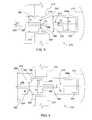
- FIG. 1Ais a top view of an exemplary embodiment of a MEMS device disclosed herein.
- FIG. 1Bis a side elevation view of the MEMS device shown in FIG. 1A along the line A-A′.
- FIG. 1Cis a side elevation view of the MEMS device shown in FIG. 1A along the line B-B′.
- FIG. 2is a top view of an embodiment of a MEMS device disclosed herein.
- FIG. 3is an enlarged top partial view of an embodiment of a MEMS device disclosed herein.
- FIG. 4is an enlarged top partial view of an embodiment of a MEMS device disclosed herein.
- the MEMS device 10can include a MEMS actuator 12 and an actuable element 14 .
- the MEMS actuator 12can be an electromagnetic actuator, as described in greater detail in U.S. patent application Ser. No. 10/079,985, incorporated herein by reference in its entirety.
- the MEMS actuatormay be another type of MEMS actuator such as, for example, an electrostatic, thermal, or piezoelectric actuator.
- the illustrated MEMS actuator 12can include an electrically conductive coil arranged to generate a magnetic field within a gap 8 formed by the spaced-apart ends of the actuator 12 upon application of a current to the coil, as by first electrically conducting lead 18 and a second electrically conducting lead 19 .
- the actuable element 14may be shaped to include a base 20 and an elongated arm 22 that can be coupled to and extend from the base 20 .
- the base 20 or other portion of the actuable element 14may include a layer or portion of magnetic material.
- the base 20 of the actuable element 14may be positioned proximate the gap 8 such that the base 20 can be displaced relative to the gap 8 upon application of a magnetic field on the magnetic material of the actuable element 14 .
- a cantilever 24 or more than one cantilever 24 , or other mechanism for controlling the displacement of the actuable elementmay be coupled to the actuable element 14 at one end and to the substrate 54 at another end.
- the MEMS actuator 12can be constructed on the surface of the substrate 54 and the actuable element 14 and the cantilever 24 can be constructed from the substrate 54 , preferably from a top device layer 52 of the substrate 54 in the case of a Silicon-on-Insulator (SOI) wafer.
- SOISilicon-on-Insulator
- the actuable element 14 and the cantilever 24may be suspended over a cavity 16 (denoted by crosshatching in FIG. 1A ) in the substrate 54 and thus may be free to be displaced relative to the substrate 54 along a displacement axis 26 .
- the actuator 12may be constructed from one or more layers of the substrate 54 to reduce the extent of the MEMS device 10 in a direction perpendicular from the substrate surface.
- actuable element 14may derail from the displacement axis 26 , or the base 20 may be dislodged from its position adjacent gap 8 .
- stops 28may be constructed from one or more layers of substrate 54 so as to limit the movement of actuable element 14 , particularly during and following wet etching.
- actuable element 14can be seen to extend along displacement axis 26 within a trench, or channel, 30 formed by sidewalls 32 , 34 , which can extend the depth of SOI device layer 52 .
- Sidewalls 32 , 34may be spaced a distance w from actuable element 14 , such that actuable element 14 may be generally centered in channel 30 .
- Sidewall 32can have an opening 36 therein to permit the cantilever 24 to connect to the actuable element 14 .
- Sidewall 34can have an indented portion 38 extending a distance y along the displacement axis 26 , where sidewall 34 can be displaced a distance/further from displacement axis 26 than other portions of sidewall 34 .
- One or more stops 28can be formed by the opposing faces of the indented portion 38 , the opposing faces being oriented generally perpendicular to the displacement axis 26 .
- Actuable element 14may have a stop arm 40 that can extend from actuable element 14 toward sidewall 34 so as to be between stops 28 .
- movement of actuable element 14 along displacement axis 26may be restricted to the movement of stop arm 40 between stops 28 .
- the distance ycan be chosen such that the movement of actuable element 14 between stops 28 is sufficient for normal operation of MEMS device 10 , yet can constrain movement of actuable element, particularly during the wet etching process, to restrict derailing or dislodging of actuable element 14 from channel 30 .
- stops 28 and/or stop arm 40can have a dimple 42 formed thereon, which can minimize stiction between actuable element 14 and stop 28 when actuable element 14 can contact stop 28 .
- a dimple 42may have a curved or angled contact surface that is configured to limit the amount of surface area contact between the contact surface of the dimple 42 and a surface of a component of a MEMS device.
- contact surfaces of stop arm 40 and/or stops 28may be textured and/or an anti-stiction coating may be applied thereto to minimize stiction.
- DRIEdeep reactive ion etching
- sidewall 32may be shown a distance w from actuable element 14 .
- stops 28can require only that one sidewall be indented to form the stops 28 .
- MEMS device 10may include only sidewall 34 and sidewall 32 may not be present, or may be located other than the distance w from actuable element 14 .
- stop arm 40may be located on actuable element 14 opposite to where cantilever 24 couples to actuable element 14 , though other locations of stop arm 40 and stops 28 along displacement axis 26 may provide satisfactory control of movements during fabrication of MEMS device 10 .
- FIG. 2can show a top view of another exemplary embodiment of a MEMS device 110 .
- actuable element 114can include an offset portion 144 in which the displacement axis 126 and elongated arm 122 can be offset, as indicated by offset displacement axis 126 a and offset elongated arm portion 122 a .
- Offset portion 144can have a width x that can encompass elongated arm portion 122 and its offset 122 a .
- Offset portion 144can form offset faces 144 a and 144 b at opposite ends of offset portion 144 .
- Sidewalls 132 , 134may be similarly offset such that channel 130 can be offset, as indicated by offset channel 130 a , to form stops 128 a and 128 b that may be opposed to respective offset faces 144 a , 144 b .
- movement of actuable element 114can be limited by faces 144 a and 144 b contacting respective stops 128 a and 128 b.
- measurescan be taken to minimize stiction between offset faces 144 a , 114 b and respective stops 128 a , 128 b .
- stops 128 a , 128 b and/or offset faces 144 a , 144 bcan have dimples 142 formed thereon to minimize stiction between stops 128 a , 128 b and offset faces 144 a , 144 b when the offset faces 144 a , 144 b can contact stops 128 a , 128 b .
- offset faces 144 a , 144 b and/or stops 128 a , 128 bmay be textured and/or an anti-stiction coating may be applied thereto.
- Other methodsas previously described, may also be used to minimize stiction.
- offset portion 144 and sidewalls 132 , 134can be correspondingly shaped to maintain a width w between actuable element 114 and sidewalls 132 , 134 generally constant. Other shapes that may serve to maintain a nearly constant width or distance between sidewalls 132 , 134 and actuable element 114 may also be used.
- cantilever 124can be coupled to offset portion 144 .
- FIG. 3shows an enlarged top partial view of another exemplary embodiment of a MEMS device 210 .
- the base portion 220 of actuable element 214can have a width w 1 , greater than the width w 2 of elongated arm 222 .
- Channel 230which may pass through gap 208 , can have a first extent d 1 , which can be greater than width w 1 .
- Stops 228can be located at gap 208 on both sides of displacement axis 226 and can reduce the extent of channel 230 at stops 228 to an extent of d 2 , where d 2 may be less than w 1 but greater than w 2 .
- movement of actuable element 214 along displacement axis 226 in a first direction corresponding to arrow 246can be limited by contact between base portion 220 and stops 228 . Movement in the opposite direction may be limited by contact between base portion 220 and end 230 a of channel 230 , or between base portion 220 and actuator 212 when channel 230 may extend to actuator 212 .
- the stops 228may be symmetric about displacement axis 226 .
- stops 228extend unequally into channel 230 , may have only a single stop 228 to one side of displacement axis 226 , or may have stops 228 that may not be located opposite one another along axis 226 .
- FIG. 4illustrates an enlarged top partial view of another exemplary embodiment of a MEMS device 310 .
- Stops 328may be located along channel 330 , which may pass through gap 308 .
- Stops 328extend into channel 330 from opposing sidewalls 332 , 334 to reduce an extent of the channel 330 to an extent of d 3 between stops 328 , where d 3 can be greater than a width w 2 of actuable element 314 .
- Tabs 348can extend from actuable element 314 towards sidewalls 332 , 334 to increase the width of actuable element 314 from w 2 to a width of w 3 at tabs 348 , where w 3 may be greater than d 3 .
- movement of actuable element 314 along displacement axis 326 in a first direction corresponding to arrow 346can be limited by contact between tabs 348 and stops 328 .
- Movement in the opposite directionmay be limited by contact between base portion 320 and end 330 a of channel 330 , or between base portion 320 and actuator 312 when channel 330 may extend to actuator 312 .
- the tabs 348 and/or the stops 328may be symmetric about displacement axis 326 .
- Other modes of fabrication, operation and/or design preferencemay have the tabs 348 and/or stops 328 extend unequally and/or unsymmetrically into channel 330 , provided that contact may still be made between tabs 348 and stops 328 .
- measurescan be taken to minimize stiction between contacting surfaces of stops 228 and base portion 220 , of stops 328 and tabs 348 and of base portion 220 , 320 and actuator 212 , 312 .
- Such measurescan include providing dimples 242 , 342 on one or both of the contacting surfaces, texturing one or both of the contacting surfaces, applying an anti-stiction coating to one or both of the contacting surfaces and/or other methods, as previously described.
Landscapes
- Engineering & Computer Science (AREA)
- Physics & Mathematics (AREA)
- Electromagnetism (AREA)
- Power Engineering (AREA)
- Mechanical Engineering (AREA)
- General Engineering & Computer Science (AREA)
- Computer Hardware Design (AREA)
- Microelectronics & Electronic Packaging (AREA)
- Micromachines (AREA)
Abstract
Description
Claims (27)
Priority Applications (3)
| Application Number | Priority Date | Filing Date | Title |
|---|---|---|---|
| US10/309,964US6900510B2 (en) | 2002-02-21 | 2002-12-04 | MEMS devices and methods for inhibiting errant motion of MEMS components |
| AU2003215222AAU2003215222A1 (en) | 2002-02-21 | 2003-02-13 | Mems devices and methods of manufacture |
| PCT/US2003/004440WO2003072486A2 (en) | 2002-02-21 | 2003-02-13 | Mems devices and methods of manufacture |
Applications Claiming Priority (2)
| Application Number | Priority Date | Filing Date | Title |
|---|---|---|---|
| US10/079,985US6717227B2 (en) | 2002-02-21 | 2002-02-21 | MEMS devices and methods of manufacture |
| US10/309,964US6900510B2 (en) | 2002-02-21 | 2002-12-04 | MEMS devices and methods for inhibiting errant motion of MEMS components |
Related Parent Applications (1)
| Application Number | Title | Priority Date | Filing Date |
|---|---|---|---|
| US10/079,985Continuation-In-PartUS6717227B2 (en) | 2002-02-21 | 2002-02-21 | MEMS devices and methods of manufacture |
Publications (2)
| Publication Number | Publication Date |
|---|---|
| US20030155841A1 US20030155841A1 (en) | 2003-08-21 |
| US6900510B2true US6900510B2 (en) | 2005-05-31 |
Family
ID=46281659
Family Applications (1)
| Application Number | Title | Priority Date | Filing Date |
|---|---|---|---|
| US10/309,964Expired - Fee RelatedUS6900510B2 (en) | 2002-02-21 | 2002-12-04 | MEMS devices and methods for inhibiting errant motion of MEMS components |
Country Status (1)
| Country | Link |
|---|---|
| US (1) | US6900510B2 (en) |
Cited By (3)
| Publication number | Priority date | Publication date | Assignee | Title |
|---|---|---|---|---|
| US7417307B2 (en) | 2005-07-29 | 2008-08-26 | Hewlett-Packard Development Company, L.P. | System and method for direct-bonding of substrates |
| US20100223997A1 (en)* | 2009-03-09 | 2010-09-09 | Freescale Semiconductor, Inc. | Accelerometer with over-travel stop structure |
| US10427934B1 (en)* | 2017-03-23 | 2019-10-01 | United States Of America As Represented By The Secretary Of The Air Force | Thermal management using microelectromechanical systems bimorph cantilever beams |
Families Citing this family (1)
| Publication number | Priority date | Publication date | Assignee | Title |
|---|---|---|---|---|
| JP2008191537A (en)* | 2007-02-07 | 2008-08-21 | Canon Inc | Vibrating element and optical deflector including the vibrating element |
Citations (29)
| Publication number | Priority date | Publication date | Assignee | Title |
|---|---|---|---|---|
| US5206983A (en) | 1991-06-24 | 1993-05-04 | Wisconsin Alumni Research Foundation | Method of manufacturing micromechanical devices |
| US5629918A (en) | 1995-01-20 | 1997-05-13 | The Regents Of The University Of California | Electromagnetically actuated micromachined flap |
| US5644177A (en) | 1995-02-23 | 1997-07-01 | Wisconsin Alumni Research Foundation | Micromechanical magnetically actuated devices |
| US5778513A (en) | 1996-02-09 | 1998-07-14 | Denny K. Miu | Bulk fabricated electromagnetic micro-relays/micro-switches and method of making same |
| US5808384A (en) | 1997-06-05 | 1998-09-15 | Wisconsin Alumni Research Foundation | Single coil bistable, bidirectional micromechanical actuator |
| US5909078A (en) | 1996-12-16 | 1999-06-01 | Mcnc | Thermal arched beam microelectromechanical actuators |
| US5929542A (en) | 1997-02-03 | 1999-07-27 | Honeywell Inc. | Micromechanical stepper motor |
| US5994816A (en) | 1996-12-16 | 1999-11-30 | Mcnc | Thermal arched beam microelectromechanical devices and associated fabrication methods |
| WO2000005734A1 (en) | 1998-07-23 | 2000-02-03 | Bh Electronics, Inc. | Ultra-miniature magnetic device |
| US6085016A (en) | 1998-06-15 | 2000-07-04 | Lucent Technologies, Inc. | Magnetically controlled variable optical attenuator |
| US6087743A (en) | 1998-09-10 | 2000-07-11 | Wisconsin Alumni Research Foundation | Position control system for use with micromechanical actuators |
| US6122149A (en) | 1997-06-24 | 2000-09-19 | Seagate Technology, Inc. | Magnetic microactuator and inductive sensor having shaped pole configuration |
| US6137941A (en) | 1998-09-03 | 2000-10-24 | Lucent Technologies, Inc. | Variable optical attenuator |
| US6163643A (en) | 1998-08-12 | 2000-12-19 | Lucent Technologies Inc. | Micro-mechanical variable optical attenuator |
| US6166478A (en) | 1999-06-04 | 2000-12-26 | The Board Of Trustees Of The University Of Illinois | Method for assembly of microelectromechanical systems using magnetic actuation |
| US6173105B1 (en) | 1998-11-20 | 2001-01-09 | Lucent Technologies | Optical attenuator |
| US6171886B1 (en)* | 1998-06-30 | 2001-01-09 | Eastman Kodak Company | Method of making integrated hybrid silicon-based micro-actuator devices |
| EP1081722A2 (en) | 1999-09-03 | 2001-03-07 | Canon Kabushiki Kaisha | Electromagnetic actuator, its manufacturing method, and optical scanner using the same electromagnetic actuator |
| US6222954B1 (en) | 1999-09-17 | 2001-04-24 | Light Bytes, Inc. | Fault-tolerant fiber-optical beam control modules |
| US6246826B1 (en) | 1999-09-02 | 2001-06-12 | Nortel Networks Limited | Variable optical attenuator with profiled blade |
| US6255757B1 (en) | 1999-09-01 | 2001-07-03 | Jds Uniphase Inc. | Microactuators including a metal layer on distal portions of an arched beam |
| US6262463B1 (en) | 1999-07-08 | 2001-07-17 | Integrated Micromachines, Inc. | Micromachined acceleration activated mechanical switch and electromagnetic sensor |
| US6265239B1 (en) | 1997-12-22 | 2001-07-24 | Agere Systems Optoelectronics Guardian Corp. | Micro-electro-mechanical optical device |
| US6275320B1 (en) | 1999-09-27 | 2001-08-14 | Jds Uniphase, Inc. | MEMS variable optical attenuator |
| US6285504B1 (en) | 1999-04-30 | 2001-09-04 | Jds Uniphase Inc. | Variable optical filter |
| US6300619B1 (en) | 1997-12-22 | 2001-10-09 | Lucent Technologies Inc. | Micro-electro-mechanical optical device |
| US6308631B1 (en) | 2000-07-20 | 2001-10-30 | The United States Of America As Represented By The Secretary Of The Navy | Mems vertical to horizontal motion translation device |
| US6327855B1 (en) | 2000-02-04 | 2001-12-11 | Jds Uniphase Inc. | Actuators including serpentine arrangements of alternating actuating and opposing segments and related methods |
| EP1164601A2 (en) | 2000-06-16 | 2001-12-19 | Canon Kabushiki Kaisha | Electromagnetic actuator, its manufacturing method, and optical scanner using the same actuator |
Family Cites Families (1)
| Publication number | Priority date | Publication date | Assignee | Title |
|---|---|---|---|---|
| US6171866B1 (en)* | 1998-09-30 | 2001-01-09 | Avl Medical Instruments | Luminescence indicator for determining calcium ions |
- 2002
- 2002-12-04USUS10/309,964patent/US6900510B2/ennot_activeExpired - Fee Related
Patent Citations (31)
| Publication number | Priority date | Publication date | Assignee | Title |
|---|---|---|---|---|
| US5206983A (en) | 1991-06-24 | 1993-05-04 | Wisconsin Alumni Research Foundation | Method of manufacturing micromechanical devices |
| US5327033A (en) | 1991-06-24 | 1994-07-05 | Wisconsin Alumni Research Foundation | Micromechanical magnetic devices |
| US5629918A (en) | 1995-01-20 | 1997-05-13 | The Regents Of The University Of California | Electromagnetically actuated micromachined flap |
| US5644177A (en) | 1995-02-23 | 1997-07-01 | Wisconsin Alumni Research Foundation | Micromechanical magnetically actuated devices |
| US5778513A (en) | 1996-02-09 | 1998-07-14 | Denny K. Miu | Bulk fabricated electromagnetic micro-relays/micro-switches and method of making same |
| US5994816A (en) | 1996-12-16 | 1999-11-30 | Mcnc | Thermal arched beam microelectromechanical devices and associated fabrication methods |
| US5909078A (en) | 1996-12-16 | 1999-06-01 | Mcnc | Thermal arched beam microelectromechanical actuators |
| US6324748B1 (en) | 1996-12-16 | 2001-12-04 | Jds Uniphase Corporation | Method of fabricating a microelectro mechanical structure having an arched beam |
| US5929542A (en) | 1997-02-03 | 1999-07-27 | Honeywell Inc. | Micromechanical stepper motor |
| US5808384A (en) | 1997-06-05 | 1998-09-15 | Wisconsin Alumni Research Foundation | Single coil bistable, bidirectional micromechanical actuator |
| US6122149A (en) | 1997-06-24 | 2000-09-19 | Seagate Technology, Inc. | Magnetic microactuator and inductive sensor having shaped pole configuration |
| US6300619B1 (en) | 1997-12-22 | 2001-10-09 | Lucent Technologies Inc. | Micro-electro-mechanical optical device |
| US6265239B1 (en) | 1997-12-22 | 2001-07-24 | Agere Systems Optoelectronics Guardian Corp. | Micro-electro-mechanical optical device |
| US6085016A (en) | 1998-06-15 | 2000-07-04 | Lucent Technologies, Inc. | Magnetically controlled variable optical attenuator |
| US6171886B1 (en)* | 1998-06-30 | 2001-01-09 | Eastman Kodak Company | Method of making integrated hybrid silicon-based micro-actuator devices |
| WO2000005734A1 (en) | 1998-07-23 | 2000-02-03 | Bh Electronics, Inc. | Ultra-miniature magnetic device |
| US6163643A (en) | 1998-08-12 | 2000-12-19 | Lucent Technologies Inc. | Micro-mechanical variable optical attenuator |
| US6137941A (en) | 1998-09-03 | 2000-10-24 | Lucent Technologies, Inc. | Variable optical attenuator |
| US6087743A (en) | 1998-09-10 | 2000-07-11 | Wisconsin Alumni Research Foundation | Position control system for use with micromechanical actuators |
| US6173105B1 (en) | 1998-11-20 | 2001-01-09 | Lucent Technologies | Optical attenuator |
| US6285504B1 (en) | 1999-04-30 | 2001-09-04 | Jds Uniphase Inc. | Variable optical filter |
| US6166478A (en) | 1999-06-04 | 2000-12-26 | The Board Of Trustees Of The University Of Illinois | Method for assembly of microelectromechanical systems using magnetic actuation |
| US6262463B1 (en) | 1999-07-08 | 2001-07-17 | Integrated Micromachines, Inc. | Micromachined acceleration activated mechanical switch and electromagnetic sensor |
| US6255757B1 (en) | 1999-09-01 | 2001-07-03 | Jds Uniphase Inc. | Microactuators including a metal layer on distal portions of an arched beam |
| US6246826B1 (en) | 1999-09-02 | 2001-06-12 | Nortel Networks Limited | Variable optical attenuator with profiled blade |
| EP1081722A2 (en) | 1999-09-03 | 2001-03-07 | Canon Kabushiki Kaisha | Electromagnetic actuator, its manufacturing method, and optical scanner using the same electromagnetic actuator |
| US6222954B1 (en) | 1999-09-17 | 2001-04-24 | Light Bytes, Inc. | Fault-tolerant fiber-optical beam control modules |
| US6275320B1 (en) | 1999-09-27 | 2001-08-14 | Jds Uniphase, Inc. | MEMS variable optical attenuator |
| US6327855B1 (en) | 2000-02-04 | 2001-12-11 | Jds Uniphase Inc. | Actuators including serpentine arrangements of alternating actuating and opposing segments and related methods |
| EP1164601A2 (en) | 2000-06-16 | 2001-12-19 | Canon Kabushiki Kaisha | Electromagnetic actuator, its manufacturing method, and optical scanner using the same actuator |
| US6308631B1 (en) | 2000-07-20 | 2001-10-30 | The United States Of America As Represented By The Secretary Of The Navy | Mems vertical to horizontal motion translation device |
Non-Patent Citations (17)
| Title |
|---|
| Bhansali et al., "Prototype Feedback-Controlled Bidirectional Actuation System for MEMS Applications," Journal of Microelectromechanical Systems, 9 (2): 245-251 (Jun. 2000). |
| Christenson and Guckel, "An Electromagnetic Micro Dynamometer," 1995 IEEE MEMS Proceedings, Amsterdam, the Netherlands, pp. 386-391, Jan. 29-Feb. 2, 1995. |
| Gong and Zhou, "Micromachined Electromagnetic Actuator," Proceedings of the International Symposium on Test & Measurement, ISTM, pp. 23-26 (1999). |
| Guckel et al., "Design and Testing of Planar Magnetic Micromotors Fabricated by Deep X-Ray Lithography and Electroplating," The 7<SUP>th </SUP>International Conference on Solid-State Sensors and Actuators, Yokohama, Japan, pp. 76-79, (Jun. 7-10, 1993). |
| Guckel et al., "Electromagnetic, Spring Constrained Linear Actuator with Large Throw," Actuator'94, pp. 52-55, (Bremen, Germany Jun. 15-17, 1994). |
| Guckel et al., "Fabrication and Testing of the Planar Magnetic Micromotor," J. Micromech. Microeng. 1: 135-138, (1991). |
| Guckel et al., "Laterally Driven Electromagnetic Actuators," Solid-State Sensor and Actuator Workshop, Hilton Head, South Carolina, pp. 49-52 (Jun. 13-16, 1994). |
| Guckel et al., "Micro Electromagnetic Actuators Based on Deep X-Ray Lithography," International Symposium on Microsystems, Intelligent Materials and Robots, Sendai, Japan, Sep. 27-29, (1995) (Abstract). |
| Guckel et al., "Micromechanics for Actuators Via Deep X-Ray Lithography," SPIE vol. 2194, pp. 2-10. |
| Guckel et al., "Processing and Design Considerations for High Force Output- Large Throw Electrostatics, Linear Microactuators," Actuator 94, Bremen, Germany pp. 105-108, (Jun. 15-17, 1994) (Abstract). |
| H. Guckel and University of Wisconsin, Madison, "Photograph of Actuator," online, retrieved on Feb. 1, 2002 from URL http://mems.engr.wisc.edu/images/linear/intgrated_coil.jpg. |
| Miyajima et al., "A Durable, Shock-Resistant Electromagnetic Optical Scanner with Polyimide-Based Hinges," Journal of Microelectromechanical Systems 10 (3): 418-424, (Sep. 2001). |
| Ohnstein et al., "Tunable IR Filters with Integral Electromagnetic Actuators," Solid-State Sensor and Actuator Workshop, Hilton Head, South Carolina, pp. 196-199. (Jun. 2-6, 1996). |
| Sadler et al., "A New Electromagnetic Actuator Using Through-Hole Plating of Nickel/Iron Permalloy," Electrochemical Society Proceedings vol. 98(20): 377-388. |
| Sadler et al., "A Universal Electromagnetic Microactuator Using Magnetic Interconnection Concepts," Journal of Microelectromechanical Systems 9(4): 460-468, (Dec. 2000). |
| Stephen Cohen, "Novel VOAs Provide More Speed and Utility," Laser Focus World, pp. 139-146 (Nov. 2000). |
| Wright et al., "A Large-Force, Fully-Integrated MEMS Magnetic Actuator," Transducers 97, International Conference on Solid-State Sensors and Actuators, pp. 793-796, (Chicago, Jun. 16-19, 1997). |
Cited By (6)
| Publication number | Priority date | Publication date | Assignee | Title |
|---|---|---|---|---|
| US7417307B2 (en) | 2005-07-29 | 2008-08-26 | Hewlett-Packard Development Company, L.P. | System and method for direct-bonding of substrates |
| US20080280398A1 (en)* | 2005-07-29 | 2008-11-13 | Haluzak Charles C | System And Method For Direct Bonding Of Substrates |
| US7741157B2 (en) | 2005-07-29 | 2010-06-22 | Hewlett-Packard Development Company, L.P. | System and method for direct bonding of substrates |
| US20100223997A1 (en)* | 2009-03-09 | 2010-09-09 | Freescale Semiconductor, Inc. | Accelerometer with over-travel stop structure |
| US8186220B2 (en) | 2009-03-09 | 2012-05-29 | Freescale Semiconductor, Inc. | Accelerometer with over-travel stop structure |
| US10427934B1 (en)* | 2017-03-23 | 2019-10-01 | United States Of America As Represented By The Secretary Of The Air Force | Thermal management using microelectromechanical systems bimorph cantilever beams |
Also Published As
| Publication number | Publication date |
|---|---|
| US20030155841A1 (en) | 2003-08-21 |
Similar Documents
| Publication | Publication Date | Title |
|---|---|---|
| KR100738064B1 (en) | MEMS element with spring of nonlinear restoring force | |
| US6438954B1 (en) | Multi-directional thermal actuator | |
| US6531947B1 (en) | Direct acting vertical thermal actuator with controlled bending | |
| US6483419B1 (en) | Combination horizontal and vertical thermal actuator | |
| KR101288214B1 (en) | Mems mirror with tip or piston motion for use in adaptive optics | |
| KR100845398B1 (en) | Actuator | |
| US6650806B2 (en) | Compliant push/pull connector microstructure | |
| US6864618B2 (en) | Method for operating a microelectromechanical system using a stiff coupling | |
| US6366414B1 (en) | Micro-electro-mechanical optical device | |
| US6130464A (en) | Latching microaccelerometer | |
| KR20040021690A (en) | A microelectromechanical device having a stiffened support beam, and methods of forming stiffened support beams in mems | |
| JP3723431B2 (en) | Micro electromechanical optical device | |
| KR100313389B1 (en) | Micro Actuator and Manufacturing Method Thereof | |
| US20210198096A1 (en) | Enhanced control of shuttle mass motion in mems devices | |
| US7732975B1 (en) | Biased gap-closing actuator | |
| KR100871268B1 (en) | Thermal out-of-plane buckle-beam actuator | |
| JP2002321196A (en) | Micro structure, micro mechanical quantity sensor, micro actuator, micro optical deflector, optical scanning display, and manufacturing method thereof | |
| US6900510B2 (en) | MEMS devices and methods for inhibiting errant motion of MEMS components | |
| JP2002216606A (en) | Micromini electromechanical switch | |
| US20050104144A1 (en) | Method and apparatus to reduce parasitic forces in electro-mechanical systems | |
| US7253550B2 (en) | Torsional electrostatic actuator | |
| KR20030067491A (en) | Resonant thermal out-of-plane buckle-beam actuator | |
| US6801682B2 (en) | Latching apparatus for a MEMS optical switch | |
| US6858911B2 (en) | MEMS actuators | |
| KR100444212B1 (en) | a microactuator and manufacturing methods of the same |
Legal Events
| Date | Code | Title | Description |
|---|---|---|---|
| AS | Assignment | Owner name:FITEL TECHNOLOGIES, INC., NEW JERSEY Free format text:ASSIGNMENT OF ASSIGNORS INTEREST;ASSIGNOR:TAMURA, HIROKAZU;REEL/FRAME:013550/0412 Effective date:20021126 | |
| AS | Assignment | Owner name:ADVANCED MICROSENSORS, MASSACHUSETTS Free format text:ASSIGNMENT OF ASSIGNORS INTEREST;ASSIGNORS:ZHE, JIANG;SIDMAN, ALAN L.;NEAL, MATTHEW J.;REEL/FRAME:014050/0325 Effective date:20021126 | |
| AS | Assignment | Owner name:FURUKAWA AMERICA, INC., NEW JERSEY Free format text:CHANGE OF NAME;ASSIGNOR:FITEL TECHNOLOGIES, INC.;REEL/FRAME:013715/0792 Effective date:20030131 | |
| FPAY | Fee payment | Year of fee payment:4 | |
| AS | Assignment | Owner name:ADVANCED MICROSENSORS CORPORATION, NEW YORK Free format text:ASSIGNMENT OF ASSIGNORS INTEREST;ASSIGNOR:ADVANCED MICROSENSORS, INC.;REEL/FRAME:026360/0211 Effective date:20110523 | |
| AS | Assignment | Owner name:RENN CAPITAL GROUP, INC., TEXAS Free format text:SECURITY AGREEMENT;ASSIGNOR:ADVANCED MICROSENSORS CORPORATION;REEL/FRAME:026366/0545 Effective date:20110523 | |
| AS | Assignment | Owner name:ADVANCED MICROSENSORS CORPORATION, NEW YORK Free format text:ASSIGNMENT OF ASSIGNORS INTEREST;ASSIGNOR:ADVANCED MICROSENSORS, INC.;REEL/FRAME:026687/0159 Effective date:20110523 | |
| FPAY | Fee payment | Year of fee payment:8 | |
| SULP | Surcharge for late payment | Year of fee payment:7 | |
| AS | Assignment | Owner name:HERCULES TECHNOLOGY GROWTH CAPITAL, INC., CALIFORN Free format text:SECURITY AGREEMENT;ASSIGNOR:ADVANCED MICROSENSORS CORPORATION;REEL/FRAME:031694/0152 Effective date:20130508 | |
| REMI | Maintenance fee reminder mailed | ||
| LAPS | Lapse for failure to pay maintenance fees | ||
| STCH | Information on status: patent discontinuation | Free format text:PATENT EXPIRED DUE TO NONPAYMENT OF MAINTENANCE FEES UNDER 37 CFR 1.362 | |
| FP | Lapsed due to failure to pay maintenance fee | Effective date:20170531 |