US6898721B2 - Clock generation systems and methods - Google Patents
Clock generation systems and methodsDownload PDFInfo
- Publication number
- US6898721B2 US6898721B2US09/887,905US88790501AUS6898721B2US 6898721 B2US6898721 B2US 6898721B2US 88790501 AUS88790501 AUS 88790501AUS 6898721 B2US6898721 B2US 6898721B2
- Authority
- US
- United States
- Prior art keywords
- clock
- processor core
- processor
- frequency
- unit
- Prior art date
- Legal status (The legal status is an assumption and is not a legal conclusion. Google has not performed a legal analysis and makes no representation as to the accuracy of the status listed.)
- Expired - Lifetime, expires
Links
Images


Classifications
- G—PHYSICS
- G06—COMPUTING OR CALCULATING; COUNTING
- G06F—ELECTRIC DIGITAL DATA PROCESSING
- G06F1/00—Details not covered by groups G06F3/00 - G06F13/00 and G06F21/00
- G06F1/26—Power supply means, e.g. regulation thereof
- G06F1/32—Means for saving power
- G06F1/3203—Power management, i.e. event-based initiation of a power-saving mode
- G06F1/3234—Power saving characterised by the action undertaken
- G06F1/324—Power saving characterised by the action undertaken by lowering clock frequency
- G—PHYSICS
- G06—COMPUTING OR CALCULATING; COUNTING
- G06F—ELECTRIC DIGITAL DATA PROCESSING
- G06F1/00—Details not covered by groups G06F3/00 - G06F13/00 and G06F21/00
- G06F1/04—Generating or distributing clock signals or signals derived directly therefrom
- G06F1/08—Clock generators with changeable or programmable clock frequency
- G—PHYSICS
- G06—COMPUTING OR CALCULATING; COUNTING
- G06F—ELECTRIC DIGITAL DATA PROCESSING
- G06F1/00—Details not covered by groups G06F3/00 - G06F13/00 and G06F21/00
- G06F1/26—Power supply means, e.g. regulation thereof
- G06F1/32—Means for saving power
- G—PHYSICS
- G06—COMPUTING OR CALCULATING; COUNTING
- G06F—ELECTRIC DIGITAL DATA PROCESSING
- G06F1/00—Details not covered by groups G06F3/00 - G06F13/00 and G06F21/00
- G06F1/26—Power supply means, e.g. regulation thereof
- G06F1/32—Means for saving power
- G06F1/3203—Power management, i.e. event-based initiation of a power-saving mode
- G06F1/3234—Power saving characterised by the action undertaken
- G06F1/329—Power saving characterised by the action undertaken by task scheduling
- G—PHYSICS
- G06—COMPUTING OR CALCULATING; COUNTING
- G06F—ELECTRIC DIGITAL DATA PROCESSING
- G06F1/00—Details not covered by groups G06F3/00 - G06F13/00 and G06F21/00
- G06F1/26—Power supply means, e.g. regulation thereof
- G06F1/32—Means for saving power
- G06F1/3203—Power management, i.e. event-based initiation of a power-saving mode
- G06F1/3234—Power saving characterised by the action undertaken
- G06F1/3296—Power saving characterised by the action undertaken by lowering the supply or operating voltage
- Y—GENERAL TAGGING OF NEW TECHNOLOGICAL DEVELOPMENTS; GENERAL TAGGING OF CROSS-SECTIONAL TECHNOLOGIES SPANNING OVER SEVERAL SECTIONS OF THE IPC; TECHNICAL SUBJECTS COVERED BY FORMER USPC CROSS-REFERENCE ART COLLECTIONS [XRACs] AND DIGESTS
- Y02—TECHNOLOGIES OR APPLICATIONS FOR MITIGATION OR ADAPTATION AGAINST CLIMATE CHANGE
- Y02D—CLIMATE CHANGE MITIGATION TECHNOLOGIES IN INFORMATION AND COMMUNICATION TECHNOLOGIES [ICT], I.E. INFORMATION AND COMMUNICATION TECHNOLOGIES AIMING AT THE REDUCTION OF THEIR OWN ENERGY USE
- Y02D10/00—Energy efficient computing, e.g. low power processors, power management or thermal management
Definitions
- the present inventionrelates to systems and methods for generating a clock signal.
- a phase-locked loop(“PLL”) is typically used to provide an output signal having a precisely controlled frequency that is synchronous with the frequency of a reference or input signal.
- an on-chip PLLcan multiply the frequency of a low frequency input (off-chip) clock to generate a high frequency output clock that is precisely synchronized with the lower frequency external clock. Due to the high clock frequency, power consumption for each device has also increased. For certain products such as laptop or notebook computers, handheld computers, cellular telephones, and other wireless personal digital assistants that are designed for situations where power outlets are not available, the conservation of power can be important.
- Bluetooth and 802.11b radiosutilize the publicly available 2.4 GHz ISM frequency band for transmission. Operation in this band does not incur usage fees or licenses and permits global use of Bluetooth and/or 802.11b devices.
- a low power reconfigurable processor coreincludes one or more processing units, each unit having a clock input that controls the performance of the unit; a wireless transceiver transmitting and receiving at a frequency based on a wireless clock input; and a controller having a plurality of clock outputs each coupled to the clock inputs of the processing units and the wireless clock input, the clock outputs being generated from a common master clock.
- the master clockcan operate at up to several Gigahertz, or the master clock can operate at the Bluetooth operating frequency, or the master clock can operate at the frequency specified by the 802.11 standard.
- the systemuses a plurality of clock signals, each independently rate controlled to single destination processing element, in a system on a chip which comprises multiple such processors.
- these clocksmay be all derivatives of a single master clock.
- the clockscan be gated versions of a master clock, thus retaining a level of synchronous relationship to each other.
- the systemcan change the clock rate of each processor independently of all the other processors, as a result of a decision or algorithm invoked in order to accomplish some goal, such as power reduction, buffer memory management, or emissions control.
- the clock rate managementmay be pre-assigned based upon tasks or routines handled by each processor, or it may be invoked as a result of external or internal system stimuli, including but not limited to user input or thermal management.
- each processor's clock ratemay or may not be performed in a centralized manner on the chip.
- Clock rate controlneed not be limited to simple clock division, but rather may be more sophisticated and flexible so as to obtain rates such as three-eighths or two-thirds of the driving clock.
- Each processing elementmay connect to other processing elements through use of buffer memories or FIFOs.
- a FIFOfor example, may support isosynchronous or even asynchronous read versus write ports, hence supporting mismatched rate processing elements.
- Advantages of the systemmay include one or more of the following.
- the systemsimplifies the maintenance of clock signal integrity and minimizes the potential for errors from parasitic reactances, impedance mismatches, crosstalk, dispersion and frequency-dependent skin losses.
- the systemalso varies the clock signal and the clock period to effectively spread undesirable frequency harmonics spurs over the frequency band because the harmonic frequency created by the clock varies over time.
- the spurious signal energy at the nominal harmonic frequencyis reduced and the energy is spread across the spectrum. As a result, spurious signals and other interferences are reduced.
- the use of a single clock generator for both processor and wireless clock generationalso reduces component count and thus lowers power dissipation. This yields the benefit of longer usage time per battery replacement or charging; reduced weight and size by use of fewer and/or smaller batteries; reduced thermal and electromagnetic emissions; and increased reliability.
- the systemis ideal for battery-operated processor-based equipment, where it is desirable to minimize battery size so that the equipment can be made small and lightweight. The reduction is due to the fact that the functional units are not kept on when they are not needed. Since CMOS technology is used, power is only consumed when a functional unit is changing state (i.e., switching). Since a functional unit is “off” when it is prevented from changing state, negligible power is consumed by that functional unit.
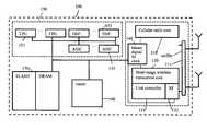
- FIG. 1is a block diagram of a single chip wireless communications integrated circuit.
- FIG. 2is a block diagram of a clock controller embodiment.
- FIG. 3is a block diagram of a first embodiment to conserve power consumption for a plurality of processing units operating in parallel.
- FIG. 4is a block diagram of a second embodiment to conserve power consumption for a plurality of processing units operating in parallel.
- FIG. 5is a block diagram of a third embodiment to conserve power consumption for a plurality of processing units operating in parallel.
- FIG. 6is a block diagram of a fourth embodiment to conserve power consumption for a plurality of processing units operating in parallel.
- FIG. 7is a block diagram of a portable computer system in accordance with the present invention.
- FIG. 1shows a block diagram of a multi-mode wireless communicator device 100 fabricated on a single silicon integrated chip.
- the device 100is an integrated CMOS device with radio frequency (RF) circuits, including a cellular radio core 110 , a short-range wireless transceiver core 130 , and a sniffer 111 , along side digital circuits, including a reconfigurable processor core 150 , a high-density memory array core 170 , and a router 190 .
- the cellular core 110 , the wireless transceiver core 130 , and the processor core 150receive clock signals from a clock controller 140 .
- the systemsimplifies the maintenance of clock signal integrity and minimizes the potential for errors from parasitic reactances, impedance mismatches, crosstalk, dispersion and frequency-dependent skin losses.
- the clock controller 140operates from the same input frequency (in this example, 2.4 GHz) and generates clocks for both digital and wireless circuits.
- the clock controller 140optimizes speed, power, and radio frequency interference considerations. For example, if the user needs to download a Web cast where data is transmitted to chip from outside wirelessly, the clock controller 140 clocks the system at maximum speed where both the processor and RF circuits are clocked at 2.4 GHz.
- the clock controller 140divides the 2.4 GHz clock down to a 1.2 GHz clock for the processor. Further, a second order harmonic of the 2.4 Ghz clock signal is used for the RF circuit. The controller 140 can also use the 2.4 GHz with a filter circuit to remove sharp clock edges for RF the circuit.
- the clock controller 140manages the generation of the clock signals to minimize undesirable EMI emissions that can cause interference.
- digital circuitsswitch quickly between predefined voltage levels, and consequently induce transient disturbances in signal and power lines, as well as energy radiated as electromagnetic waves.
- a digital circuit switching rapidly but regularly, with edges synchronous to a master clockcan generate noise with a strong spectral component at the clock frequency. Additionally, harmonics at odd multiples of the clock frequency will be generated. If the circuit remains synchronous to a master clock, but switches on random clock edges, spectral components above and below the clock frequency will also be generated.
- Digital circuitsthemselves are robust in the presence of noise from other sources. By contrast, analog circuits operate at a multiplicity of voltage levels and frequencies, and are sensitive to induced noise.
- the noise spectrum produced by dense, high-speed digital circuitscan easily interfere with high-frequency analog components. Since the waveforms transitions generated by digital circuits are, at least ideally, step transitions having (in accordance with Fourier analysis) a wide noise bandwidth, potential interference of the chip's digital signals with the chip's analog signals poses a distinct threat to circuit performance.
- the clock controller 140generates a processor clock signal at a frequency that is lower than the RF frequency (2.4 GHz in the case of Bluetooth) to avoid interference. Further, the controller 140 ensures that the edges of the clock do not generate harmonics that interfere with the 2.4 GHz frequency. In one implementation, the first harmonic of a 1.2 GHz signal is used as the 2.4 GHz carrier frequency.
- the clockis rapidly increased to 2.4 GHz with a suitable phase locked loop fed to both the processor core and the Bluetooth core.
- the edges of the clock signal generated by the PLL's voltage controlled oscillatorare phase-modulated using a random-number sequencer in order to reduce the harmonic content of the resulting clock signal.
- the digital clockcan be transformed into an analog carrier wave using a gaussian filter and a lowpass filter such as a high-order Chebyshev or Butterworth filter.
- the controller 140varies the clock signal period to effectively spread the undesirable frequency harmonics spurs over the frequency band because the harmonic frequency created by the clock varies over time.
- the clock signal periodcan be varied using techniques such as those disclosed in U.S. Pat. Nos. 5,426,392 and 5,488,627, among others. The spurious signal energy at the nominal harmonic frequency is reduced and the energy is spread across the spectrum.
- the clock tracecan be used as an antenna, radiating the signal directly from its surface, removing the need for an external antenna. This system is adapted to work with transmitter with low output power levels, such as those specified by Bluetooth (0 dBm).
- the clock tracescan also be used as a receive antenna to catch signals from a local radio source.
- the wiring tracesact as an antenna, with the clock circuit spread out over the device. Since Bluetooth power output can be increased up to a watt, a BluetoothTM transmitter can program devices even a few meters away using the clock trace antennas.
- the patch antennacan be used to get power off-chip, at least enough to power the processor clock and start the communication protocol for downloading data. For example, during wafer test, a high power 2.4 GHz signal can be beamed at the die, powering up the clock and carrying the data at the same time.
- the systemcan use Inductive Power Transfer with an AC-energized coil to create a magnetic field that couples with a receiving coil of an inductively powered device. The induced signal appearing at the output of the inductively powered device coil is then rectified and filtered to create a relatively constant DC power source.
- Inductive Power Transferwith an AC-energized coil to create a magnetic field that couples with a receiving coil of an inductively powered device.
- the induced signal appearing at the output of the inductively powered device coilis then rectified and filtered to create a relatively constant DC power source.
- MVSMagnetic Vector Steering
- HCAMHalf-Cycle Amplitude Modulation
- the high-density memory array core 170can include various memory technologies such as flash memory and dynamic random access memory (DRAM), among others, on different portions of the memory array core.
- the reconfigurable processor core 150can include one or more processors 151 such as MIPS processors and/or one or more digital signal processors (DSPs) 153 , among others.
- the reconfigurable processor core 150has a bank of efficient processors 151 and a bank of DSPs 153 with embedded functions. These processors 151 and 153 can be configured to operate optimally on specific problems.
- the bank of DSPs 153can be optimized to handle discrete cosine transforms (DCTs) or Viterbi encodings, among others.
- DCTsdiscrete cosine transforms
- Viterbi encodingsamong others.
- dedicated hardware 155can be provided to handle specific algorithms in silicon more efficiently than the programmable processors 151 and 153 .
- the number of active processorsis controlled depending on the application, so that power is not used when it is not needed. This embodiment does not rely on complex clock control methods to conserve power, since the individual clocks are not run at high speed, but rather the unused processor is simply turned off when not needed.
- One exemplary processor embedded in the multi-processor core 150includes a register bank, a multiplier, a barrel shifter, an arithmetic logic unit (ALU) and a write data register.
- the exemplary processorcan handle DSP functions by having a multiply-accumulate (MAC) unit in parallel with the ALU.
- Embodiments of the processorcan rapidly execute multiply-accumulate (MAC) and add-compare-subtract (ACS) instructions in either scalar or vector mode.
- Other parts of the exemplary processorinclude an instruction pipeline, a multiplexer, one or more instruction decoders, and a read data register.
- a program counter (PC) registeraddresses the memory system 170 .
- a program counter controllerserves to increment the program counter value within the program counter register as each instruction is executed and a new instruction must be fetched for the instruction pipeline. Also, when a branch instruction is executed, the target address of the branch instruction is loaded into the program counter by the program counter controller.
- the processor core 150incorporates data pathways between the various functional units. The lines of the data pathways may be synchronously used for writing information into the core 150 , or for reading information from the core 150 . Strobe lines can be used for this purpose.
- instructions within the instruction pipelineare decoded by one or more of the instruction decoders to produce various core control signals that are passed to the different functional elements of the processor core 150 .
- the different portions of the processor coreconduct processing operations, such as multiplication, addition, subtraction and logical operations.
- the register bankincludes a current programming status register (CPSR) and a saved programming status register (SPSR).
- CPSRcurrent programming status register
- SPSRsaved programming status register
- the current programming status registerholds various condition and status flags for the processor core 150 . These flags may include processing mode flags (e.g. system mode, user mode, memory abort mode, etc.) as well as flags indicating the occurrence of zero results in arithmetic operations, carries and the like.
- the multi-mode wireless communicator device 100can detect and communicate with any wireless system it encounters at a given frequency.
- the router 190performs the switch in real time through an engine that keeps track of the addresses of where the packets are going.
- the router 190can send packets in parallel through two or more separate pathways. For example, if a BluetoothTM connection is established, the router 190 knows which address it is looking at and will be able to immediately route packets using another connection standard. In doing this operation, the router 190 working with the RF sniffer 111 periodically scans its radio environment (‘ping’) to decide on optimal transmission medium.
- the router 190can send some packets in parallel through both the primary and secondary communication channel to make sure some of the packets arrive at their destinations.
- the reconfigurable processor core 150controls the cellular radio core 110 and the short-range wireless transceiver core 130 to provide a seamless dual-mode network integrated circuit that operates with a plurality of distinct and unrelated communications standards and protocols such as Global System for Mobile Communications (GSM), General Packet Radio Service (GPRS), Enhance Data Rates for GSM Evolution (Edge) and BluetoothTM.
- GSMGlobal System for Mobile Communications
- GPRSGeneral Packet Radio Service
- EdgeEnhance Data Rates for GSM Evolution
- BluetoothTMBluetoothTM
- the cell phone core 110provides wide area network (WAN) access, while the short-range wireless transceiver core 130 supports local area network (LAN) access.
- the reconfigurable processor core 150has embedded read-only-memory (ROM) containing software such as IEEE802.11, GSM, GPRS, Edge, and/or BluetoothTM protocol software, among others.
- ROMread-only-memory
- the cellular radio core 110includes a transmitter/receiver section that is connected to an off-chip antenna (not shown).
- the transmitter/receiver sectionis a direct conversion radio that includes an I/Q demodulator, transmit/receive oscillator/clock generator, multi-band power amplifier (PA) and PA control circuit, and voltage-controlled oscillators and synthesizers.
- IFintermediate frequency
- the transmitter/receiver sectionconverts received signals into a first intermediate frequency (IF) by mixing the received signals with a synthesized local oscillator frequency and then translates the first IF signal to a second IF signal.
- the second IF signalis hard-limited and processed to extract an RSSI signal proportional to the logarithm of the amplitude of the second IF signal.
- the hard-limited IF signalis processed to extract numerical values related to the instantaneous signal phase, which are then combined with the RSSI signal.
- the combined signalsare processed by the processor core 150 to form PCM voice samples that are subsequently converted into an analog signal and provided to an external speaker or earphone.
- the processorsimply transfers the data over an input/output (I/O) port.
- I/Oinput/output
- an off-chip microphonecaptures analog voice signals, digitizes the signal, and provides the digitized signal to the processor core 150 .
- the processor core 150codes the signal and reduces the bit-rate for transmission.
- the processor core 150converts the reduced bit-rate signals to modulated signals such as I,I,Q,Q modulating signals, for example.
- the datais modulated and the modulated signals are then fed to the cellular telephone transmitter of the transmitter/receiver section.
- the short-range wireless transceiver core 130contains a radio frequency (RF) modem core 132 that communicates with a link controller core 134 .
- the processor core 150controls the link controller core 134 .
- the RF modem core 132has a direct-conversion radio architecture with integrated VCO and frequency synthesizer.
- the RF-unit 132includes an RF receiver connected to an analog-digital converter (ADC), which in turn is connected to a modem 116 performing digital modulation, channel filtering, AFC, symbol timing recovery, and bit slicing operations.
- ADCanalog-digital converter
- the modemis connected to a digital to analog converter (DAC) that in turn drives an RF transmitter.
- DACdigital to analog converter
- the link controller core 134provides link control function and can be implemented in hardware or in firmware.
- One embodiment of the core 134is compliant with the BluetoothTM specification and processes BluetoothTM packet types.
- the link controller core 134performs a header error check, scrambles the header to randomize the data and to minimize DC bias, and performs forward error correction (FEC) encoding to reduce the chances of getting corrupted information.
- the payloadis passed through a cyclic redundancy check (CRC), encrypted/scrambled and FEC-encoded.
- CRCcyclic redundancy check
- the FEC encoded datais then inserted into the header.
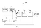
- FIG. 2shows one implementation of a clock controller 140 .
- the clock controller 140receives a reference clock signal 141 .
- the reference clock signal 141can be generated off-chip, or alternatively, can be generated on-chip using an on-chip oscillator that can be crystal controlled, resistive-capacitive (RC) controlled, or can be a ring-oscillator.
- the reference signal 141is provided to a frequency multiplier 142 .
- the frequency multiplier 142generates a clock signal at 2.4 GHz.
- the clock signalcan be supplied to both the processor core and a local oscillator for the wireless core. Since current generation of microprocessors uses frequencies in excess of 1 GHz, easily reaching the 2.4 GHz required for Bluetooth and 802.11 operation, the master clock can then be used to power the both.
- the clockcan be filtered to remove spiking edges.
- the frequency multiplier 142is a PLL with a phase detector 144 , a loop filter 145 , a voltage controlled oscillator (“VCO”) 146 , a reference divider 147 , and a feedback divider 148 .
- a low-pass filter (LPF)can be used to remove high frequency components from an error signal generated by the phase detector.
- the oscillation frequency of the VCOis controlled with the smoothed error signal to tune its output frequency to the input data.
- a fixed reference signalis transmitted to the reference divider 147 and then to one input of the phase detector 144 .
- the output of the VCO 146is divided by the feedback divider 148 and input to the other input of the phase detector 144 .
- the frequency at the output of this implementation of the frequency multiplier 142is an integer multiple of the frequency at the input of the phase detector, non-integer divider such as those in U.S. Pat. No. 6,236,278 can be used as well.
- the controller 140ensures that the edges of the clock do not generate harmonics that interfere with the 2.4 GHz frequency.
- the first harmonic of a 1.2 GHz signalis used as the 2.4 GHz carrier frequency.
- the clockis rapidly increased to 2.4 GHz with a suitable phase locked loop fed to both the processor core and the Bluetooth core.
- the edges of the clock signal generated by the PLL's voltage controlled oscillatorare phase-modulated using a random-number sequencer in order to reduce the harmonic content of the resulting clock signal.
- the digital clockcan be transformed into an analog carrier wave using a gaussian filter and a lowpass filter such as a high-order Chebyshev or Butterworth filter.
- the CPUperforms complex calculations for wireless 802.11a/b transmission, while the Bluetooth transceiver/radio or the 802.11 transceiver/radio is used for local ‘last meter’ transmission of data in a personal area network (PAN).
- PANpersonal area network
- the clock frequency used by the processor corecan be less than 2.4 GHz. This can be done by scaling down the 2.4 GHz clock signal with a clock divider. In this manner, a single clocking source can be used for a number of RF and digital operations.
- FIG. 3shows an exemplary embodiment to conserve power in a system with a plurality of processing elements or units 310 , 312 314 , 316 and 318 .
- processing units 310 - 312operate in parallel, while processing units 314 , 316 , and 318 operate in seriatim based on the previous processing unit's outputs.
- Multiple instructionsare executed at the same time in the different execution units 310 , 312 314 , 316 and 318 , as long as these instructions do not contend for the same resources (namely, shared memory).
- powercan be saved by varying the clock frequency, the core voltage or a combination thereof, if necessary, to reduce heat or to reduce battery power consumption.
- a plurality of processing unitsoperates in parallel. This embodiment relies on varying the clock signals to control power consumption.
- Each of the processing units 310 , 312 314 , 316 and 318is powered by the same voltage rail.
- a master clock 302supplies a master clock signal to a clock controller 304 .
- the clock controller 304determines for each application the appropriate clock signal that is applied to each of processing units 310 , 312 314 , 316 and 318 .
- the controller 304drives the clock input of each of processing units 310 , 312 314 , 316 and 318 .
- the clockcan be driven independently and can be based on the tasks to be performed. For example, a task-based clock scheme for an exemplary three-processor system at a particular time point is as follows:
- the tableillustrates a sequence of clock management events in a multiple processing element system. Although the figure indicates all processor clocking management to occur coincidentally, generalization of the invention to include unsynchronized and/or gradual rate changes is a simple extension of the invention. Additionally subsets of processing elements may be grouped and managed together as ensembles.
- the controller 304can be implemented in hardware; or the power control may be implemented by means of software. If a high performance operating level of the core is not required for a particular application, software instructions may be utilized to operate the power control circuit. In one implementation, switching ability is no longer provided to the processing unit after a preselected clock cycle period after the processing unit has completed the required task of executing the machine code instruction of the computer program to turned off (de-activated) the unit after it has executed the required task.
- FIG. 4is a block diagram of a second embodiment to conserve power consumption for a plurality of processing units operating in parallel. This embodiment is similar to the embodiment of FIG. 3 , except that the output of each of the sequential processing units 314 , 316 and 318 is buffered by buffers 324 , 326 and 328 , respectively.
- the buffers 324 , 326 and 328are first-in-first-out (FIFO) buffers.
- FIG. 5is a block diagram of a third embodiment to conserve power consumption for a plurality of processing units operating in parallel. This embodiment is also similar to the embodiment of FIG. 3 , with the addition of a programmable voltage source 330 .
- FIG. 6is a block diagram of a fourth embodiment similar to the embodiment of FIG. 4 , except that the buffered processing units operating in parallel at individually controlled supply voltages.
- each of the processing units 310 , 312 314 , 316 and 318is powered by independent voltage rails whose voltage can be varied within a predetermined range.
- FIG. 7illustrates an exemplary computer system 200 with the wireless communication device 100 .
- the computer system 200is preferably housed in a small, rectangular portable enclosure.
- a processor 220 or central processing unit (CPU)provides the processing capability.
- the processor 220can be a reduced instruction set computer (RISC) processor or a complex instruction set computer (CISC) processor.
- RISCreduced instruction set computer
- CISCcomplex instruction set computer
- the processor 220is a low power CPU such as the MC68328V DragonBall device available from Motorola Inc.
- the processor 220is connected to a read-only-memory (ROM) 221 for receiving executable instructions as well as certain predefined data and variables.
- the processor 220is also connected to a random access memory (RAM) 222 for storing various run-time variables and data arrays, among others.
- the RAM 222is sufficient to store user application programs and data. In this instance, the RAM 222 can be provided with a back-up battery to prevent the loss of data even when the computer system is turned off.
- non-volatile memorysuch as a programmable ROM such as an electrically erasable programmable ROM, a flash ROM memory in addition to the ROM 221 for data back-up purposes.
- the computer system 200has built-in applications stored in the ROM 221 or downloadable to the RAM 222 which include, among others, an appointment book to keep track of meetings and to-do lists, a phone book to store phone numbers and other contact information, a notepad for simple word processing applications, a world time clock which shows time around the world and city locations on a map, a database for storing user specific data, a stopwatch with an alarm clock and a countdown timer, a calculator for basic computations and financial computations, and a spreadsheet for more complex data modeling and analysis. Additionally, project planning tools, and CAD/CAM systems, Internet browsers, among others, may be added to increase the functionality of portable computing appliances. Users benefit from this software, as the software allows users to be more productive when they travel as well as when they are in their offices.
- the computer system 200receives instructions from the user via one or more switches such as push-button switches in a keypad 224 .
- the processor 220is also connected to a real-time clock/timer 225 that tracks time.
- the clock/timer 225can be a dedicated integrated circuit for tracking the real-time clock data, or alternatively, the clock/timer 225 can be a software clock where time is tracked based on the clock signal clocking the processor 220 .
- the clock/timer 225is software-based, it is preferred that the software clock/timer be interrupt driven to minimize the CPU loading. However, even an interrupt-driven software clock/timer 225 requires certain CPU overhead in tracking time.
- the real-time clock/timer integrated circuit 225is preferable where high processing performance is needed.
- the processor 220drives an internal bus 226 .
- the computer systemcan access data from the ROM 221 or RAM 222 , or can acquire I/O information such as visual information via a charged coupled device (CCD) 228 .
- CCDcharged coupled device
- the CCD unit 228is further connected to a lens assembly (not shown) for receiving and focusing light beams to the CCD for digitization. Images scanned via the CCD unit 228 can be compressed and transmitted via a suitable network such as the Internet, through Bluetooth channel, cellular telephone channels or via facsimile to a remote site.
- the processor 220is connected to the multi-mode wireless communicator device 100 , which is connected to an antenna 232 .
- the device 100satisfies the need to access electronic mail, paging, mode/facsimile, remote access to home computers and the Internet.
- the antenna 232can be a loop antenna using flat-strip conductors such as printed circuit board wiring traces as flat strip conductors have lower skin effect loss in the rectangular conductor than that of antennas with round-wire conductors.
- One simple form of wireless communication device 100is a wireless link to a cellular telephone where the user simply accesses a cellular channel similar to the making of a regular voice call. Also mention that one channel is reserved for making voice calls.
- data channelsare not usable for voice communications because of the latency and low packet reliability, so a dedicated voice channel is necessary.
- GPRSthere are a total of 8 channels per user, one of which is dedicated to voice when the user decides to make a voice call. This voice connection is independent of the data connection.
- the processor 220 of the preferred embodimentaccepts handwritings as an input medium from the user.
- a digitizer 234 , a pen 233 , and a display LCD panel 235are provided to capture the handwriting.
- the digitizer 234has a character input region and a numeral input region that are adapted to capture the user's handwritings on words and numbers, respectively.
- the LCD panel 235has a viewing screen exposed along one of the planar sides of the enclosure are provided.
- the assembly combination of the digitizer 234 , the pen 233 and the LCD panel 235serves as an input/output device. When operating as an output device, the screen 235 displays computer-generated images developed by the CPU 220 .
- the LCD panel 235also provides visual feedback to the user when one or more application software execute.
- the digitizer 234When operating as an input device, the digitizer 234 senses the position of the tip of the stylus or pen 233 on the viewing screen 235 and provides this information to the computer's processor 220 .
- the present inventioncontemplates that display assemblies capable of sensing the pressure of the stylus on the screen can be used to provide further information to the CPU 220 .
- the CPU 220accepts pen strokes from the user using the stylus or pen 233 that is positioned over the digitizer 234 .
- the position of the pen 233is sensed by the digitizer 234 via an electromagnetic field as the user writes information to the computer system.
- the digitizer 234converts the position information to graphic data. For example, graphical images can be input into the pen-based computer by merely moving the stylus over the surface of the screen.
- the CPU 220senses the position and movement of the stylus, it generates a corresponding image on the screen to create the illusion that the pen or stylus is drawing the image directly upon the screen.
- the data on the position and movement of the stylusis also provided to handwriting recognition software, which is stored in the ROM 221 and/or the RAM 222 .
- the handwriting recognizersuitably converts the written instructions from the user into text data suitable for saving time and expense information. The process of converting the pen strokes into equivalent characters and/or drawing vectors using the handwriting recognizer is described below.
- the computer systemis also connected to one or more input/output (I/O) ports 242 which allow the CPU 220 to communicate with other computers.
- I/O ports 242may be a parallel port, a serial port, a universal serial bus (USB) port, a Firewire port, or alternatively a proprietary port to enable the computer system to dock with the host computer.
- USBuniversal serial bus
- Firewire portor alternatively a proprietary port to enable the computer system to dock with the host computer.
- the I/O port 242is housed in a docking port, after docking, the I/O ports 242 and software located on a host computer (not shown) support an automatic synchronization of data between the computer system and the host computer.
- the synchronization softwareruns in the background mode on the host computer and listens for a synchronization request or command from the computer system 200 of the present invention.
- the I/O port 242is preferably a high speed serial port such as an RS-232 port, a Universal Serial Bus, or a Fibre Channel for cost reasons, but can also be a parallel port for higher data transfer rate.
- One or more portable computers 200can be dispersed in nearby cell regions and communicate with a cellular mobile support station (MSS) as well as a Bluetooth station.
- MSScellular mobile support station
- the cellular and Bluetooth stationsrelay the messages via stations positioned on a global basis to ensure that the user is connected to the network, regardless of his or her reference to home.
- the stationsare eventually connected to the Internet, which is a super-network, or a network of networks, interconnecting a number of computers together using predefined protocols to tell the computers how to locate and exchange data with one another.
- the primary elements of the Internetare host computers that are linked by a backbone telecommunications network and communicate using one or more protocols.
- the most fundamental of Internet protocolsis called Transmission Control Protocol/Internet Protocol (TCP/IP), which is essentially an envelope where data resides.
- TCP/IPTransmission Control Protocol/Internet Protocol
- the TCP protocoltells computers what is in the packet, and the IP protocol tells computers where to send the packet.
- the IPtransmits blocks of data called datagrams from sources to destinations throughout the Internet. As packets of information travel across the Internet, routers throughout the network check the addresses of data packages and determine the best route to send them to their destinations. Furthermore, packets of information are detoured around non-operative computers if necessary until the information finds its way to the proper destination.
Landscapes
- Engineering & Computer Science (AREA)
- Theoretical Computer Science (AREA)
- Physics & Mathematics (AREA)
- General Engineering & Computer Science (AREA)
- General Physics & Mathematics (AREA)
- Transceivers (AREA)
- Mobile Radio Communication Systems (AREA)
Abstract
Description
| Pro- | ||||||
| ces- | ||||||
| Task | 1 | Task 2 | Task 3 | Task 4 | Task 5 | |
| P0 | Clock | Clock | Clock*1/32 | Clock*1/32 | Clock*1/32 | |
| P1 | Clock* | Clock*2/3 | Clock*1/4 | Clock*1/16 | Clock*1/32 | |
| 1/16 | ||||||
| P2 | Clock* | Clock*5/32 | Clock*1/2 | Clock*1/2 | Clock*1/32 | |
| 1/32 | ||||||
Claims (20)
Priority Applications (2)
| Application Number | Priority Date | Filing Date | Title |
|---|---|---|---|
| US09/887,905US6898721B2 (en) | 2001-06-22 | 2001-06-22 | Clock generation systems and methods |
| US11/010,548US20050117633A1 (en) | 2001-06-22 | 2004-12-13 | Clock generation systems and methods |
Applications Claiming Priority (1)
| Application Number | Priority Date | Filing Date | Title |
|---|---|---|---|
| US09/887,905US6898721B2 (en) | 2001-06-22 | 2001-06-22 | Clock generation systems and methods |
Related Child Applications (1)
| Application Number | Title | Priority Date | Filing Date |
|---|---|---|---|
| US11/010,548ContinuationUS20050117633A1 (en) | 2001-06-22 | 2004-12-13 | Clock generation systems and methods |
Publications (2)
| Publication Number | Publication Date |
|---|---|
| US20030014682A1 US20030014682A1 (en) | 2003-01-16 |
| US6898721B2true US6898721B2 (en) | 2005-05-24 |
Family
ID=25392112
Family Applications (2)
| Application Number | Title | Priority Date | Filing Date |
|---|---|---|---|
| US09/887,905Expired - LifetimeUS6898721B2 (en) | 2001-06-22 | 2001-06-22 | Clock generation systems and methods |
| US11/010,548AbandonedUS20050117633A1 (en) | 2001-06-22 | 2004-12-13 | Clock generation systems and methods |
Family Applications After (1)
| Application Number | Title | Priority Date | Filing Date |
|---|---|---|---|
| US11/010,548AbandonedUS20050117633A1 (en) | 2001-06-22 | 2004-12-13 | Clock generation systems and methods |
Country Status (1)
| Country | Link |
|---|---|
| US (2) | US6898721B2 (en) |
Cited By (34)
| Publication number | Priority date | Publication date | Assignee | Title |
|---|---|---|---|---|
| US20030126451A1 (en)* | 2001-09-28 | 2003-07-03 | Gorobets Sergey Anatolievich | Data processing |
| US20040209575A1 (en)* | 2003-04-19 | 2004-10-21 | International Business Machines Corporation | Wireless communication system within a system on a chip |
| US20040268164A1 (en)* | 2003-06-26 | 2004-12-30 | International Business Machines Corporation | Lowered PU power usage method and apparatus |
| US20050060385A1 (en)* | 2003-09-15 | 2005-03-17 | Gupta Vivek G. | Method and apparatus for sharing a GPRS module with two computing devices |
| US20050188234A1 (en)* | 2004-02-24 | 2005-08-25 | Chi-Tung Chang | Method for automatically regulating an oscillator |
| US20050228904A1 (en)* | 2004-03-16 | 2005-10-13 | Moore Charles H | Computer processor array |
| US20060057970A1 (en)* | 2001-11-29 | 2006-03-16 | Patrick Kusbel | System and method for reducing the effects of clock harmonic frequencies |
| US20060080566A1 (en)* | 2001-03-21 | 2006-04-13 | Sherburne Robert W Jr | Low power clocking systems and methods |
| US20060095750A1 (en)* | 2004-08-30 | 2006-05-04 | Nye Jeffrey L | Processes, circuits, devices, and systems for branch prediction and other processor improvements |
| US20060222087A1 (en)* | 2005-03-31 | 2006-10-05 | Adc Telecommunications, Inc. | Methods and systems for handling underflow and overflow in a software defined radio |
| US20060222020A1 (en)* | 2005-03-31 | 2006-10-05 | Adc Telecommunications, Inc. | Time start in the forward path |
| US20060223514A1 (en)* | 2005-03-31 | 2006-10-05 | Adc Telecommunications, Inc. | Signal enhancement through diversity |
| US20060227805A1 (en)* | 2005-03-31 | 2006-10-12 | Adc Telecommunications, Inc. | Buffers handling multiple protocols |
| US7139921B2 (en) | 2001-03-21 | 2006-11-21 | Sherburne Jr Robert Warren | Low power clocking systems and methods |
| US20070001774A1 (en)* | 2005-06-29 | 2007-01-04 | Stevenson Paul E | Apparatus, system, and method for oscillator network with multiple parallel oscillator circuits |
| US7209711B2 (en) | 2001-05-14 | 2007-04-24 | Interdigital Technology Corporation | Dynamic channel quality measurement procedures for optimizing data transmission in a wireless digital communication system |
| US20070094463A1 (en)* | 2005-10-25 | 2007-04-26 | Harris Corporation, Corporation Of The State Of Delaware | Mobile wireless communications device providing data management and security features and related methods |
| US20070192646A1 (en)* | 2006-02-16 | 2007-08-16 | Moore Charles H | Asynchronous power saving computer |
| US20070281614A1 (en)* | 2006-06-01 | 2007-12-06 | Motorola, Inc. | Method and apparatus for dual mode communications |
| US20080010552A1 (en)* | 2006-05-04 | 2008-01-10 | Agere Systems Inc. | Method and apparatus for testing a dual mode interface |
| US20080137575A1 (en)* | 2005-03-31 | 2008-06-12 | Adc Telecommunications, Inc. | Dynamic reallocation of bandwidth and modulation protocols |
| US20080168199A1 (en)* | 2005-03-31 | 2008-07-10 | Adc Telecommunications, Inc. | Dynamic readjustment of power |
| US20080212728A1 (en)* | 2005-03-14 | 2008-09-04 | Lu Paul Y | Method and apparatus for generating clocks for a handheld multistandard communication system |
| US20080254784A1 (en)* | 2005-03-31 | 2008-10-16 | Adc Telecommunications, Inc. | Dynamic reconfiguration of resources through page headers |
| US20080301482A1 (en)* | 2007-05-31 | 2008-12-04 | Goff Lonnie C | Method and apparatus for connecting multiple multimode processors |
| US7463140B2 (en) | 2001-06-22 | 2008-12-09 | Gallitzin Allegheny Llc | Systems and methods for testing wireless devices |
| US20090080498A1 (en)* | 2007-09-24 | 2009-03-26 | Deisher Michael E | Adaptive radio frequency interference mitigation during channel scanning or hopping |
| US20090167451A1 (en)* | 2004-03-22 | 2009-07-02 | Mobius Microsystems, Inc. | Frequency Controller for a Monolithic Clock Generator and Timing/Frequency Reference |
| US7593450B2 (en) | 2005-03-31 | 2009-09-22 | Adc Telecommunications, Inc. | Dynamic frequency hopping |
| US20090247075A1 (en)* | 2008-03-28 | 2009-10-01 | Ahmadreza Rofougaran | Method and system for a low-complexity multi-beam repeater |
| US7904615B2 (en) | 2006-02-16 | 2011-03-08 | Vns Portfolio Llc | Asynchronous computer communication |
| FR2951598A1 (en)* | 2009-10-15 | 2011-04-22 | Sagem Comm | IP AND RADIO COMMUNICATION DEVICE WITH A SINGLE OSCILLATOR AND METHOD OF CONTROLLING THE OSCILLATOR |
| US7966481B2 (en) | 2006-02-16 | 2011-06-21 | Vns Portfolio Llc | Computer system and method for executing port communications without interrupting the receiving computer |
| US20110279424A1 (en)* | 2010-05-11 | 2011-11-17 | Himax Technologies Limited | Display device and driving circuit thereof |
Families Citing this family (27)
| Publication number | Priority date | Publication date | Assignee | Title |
|---|---|---|---|---|
| US7010621B2 (en)* | 2002-02-14 | 2006-03-07 | The Boeing Company | System having a spread-spectrum clock for further suppression of electromagnetic emissions in network devices communicating via a network bus |
| US6950672B2 (en)* | 2002-05-30 | 2005-09-27 | Analog Devices, Inc. | Clock enable system |
| US6842607B2 (en)* | 2002-09-09 | 2005-01-11 | Conexant Systems, Inc | Coordination of competing protocols |
| US7031372B2 (en)* | 2003-04-22 | 2006-04-18 | Motorola, Inc. | Multiple user reconfigurable CDMA processor |
| US7114069B2 (en)* | 2003-04-22 | 2006-09-26 | Motorola, Inc. | Reconfigurable processing circuit including a delay locked loop multiple frequency generator for generating a plurality of clock signals which are configured in frequency by a control processor |
| US7254208B2 (en)* | 2003-05-20 | 2007-08-07 | Motorola, Inc. | Delay line based multiple frequency generator circuits for CDMA processing |
| JP2007519270A (en)* | 2003-06-26 | 2007-07-12 | コーニンクレッカ フィリップス エレクトロニクス エヌ ヴィ | Method for clock synchronization of a wireless 1394 bus for nodes connected via an IEEE 802.11 LAN |
| US7480751B2 (en)* | 2003-09-08 | 2009-01-20 | Broadcom Corporation | Serial data interface system and method using a selectively accessed tone pattern generator |
| US8265563B2 (en)* | 2006-10-31 | 2012-09-11 | Hewlett-Packard Development Company, L.P. | Techniques for enhanced co-existence of co-located radios |
| US8755747B2 (en) | 2006-10-31 | 2014-06-17 | Qualcomm Incorporated | Techniques to control transmit power for a shared antenna architecture |
| US20080172238A1 (en)* | 2007-01-12 | 2008-07-17 | Yosuke Muraki | Electronic system with run-time information |
| US7917799B2 (en)* | 2007-04-12 | 2011-03-29 | International Business Machines Corporation | Method and system for digital frequency clocking in processor cores |
| US8161314B2 (en)* | 2007-04-12 | 2012-04-17 | International Business Machines Corporation | Method and system for analog frequency clocking in processor cores |
| JP2009141482A (en)* | 2007-12-04 | 2009-06-25 | Fujitsu Ltd | Clock signal transmission method and radio communication apparatus in radio communication apparatus |
| WO2010097725A1 (en)* | 2009-02-27 | 2010-09-02 | Koninklijke Philips Electronics N.V. | Methods, transmission devices and transmission control system for transmitting power wirelessly |
| US8909165B2 (en)* | 2009-03-09 | 2014-12-09 | Qualcomm Incorporated | Isolation techniques for multiple co-located radio modules |
| WO2010116538A1 (en)* | 2009-04-06 | 2010-10-14 | Hitachi, Ltd. | Storage apparatus and data transfer method |
| US9693390B2 (en) | 2009-06-01 | 2017-06-27 | Qualcomm Incorporated | Techniques to manage a mobile device based on network density |
| US8737233B2 (en)* | 2011-09-19 | 2014-05-27 | International Business Machines Corporation | Increasing throughput of multiplexed electrical bus in pipe-lined architecture |
| US9015519B2 (en)* | 2012-01-31 | 2015-04-21 | Symantec Corporation | Method and system for cluster wide adaptive I/O scheduling by a multipathing driver |
| US20130210345A1 (en)* | 2012-02-15 | 2013-08-15 | Curtis Ling | Method and system for broadband near field communication utilizing full spectrum capture |
| US10474846B1 (en) | 2017-08-31 | 2019-11-12 | Square, Inc. | Processor power supply glitch detection |
| US10476607B2 (en)* | 2017-09-30 | 2019-11-12 | Square, Inc. | Wireless signal noise reduction |
| US10255590B1 (en) | 2017-09-30 | 2019-04-09 | Square, Inc. | Radio frequency noise management |
| US20220276828A1 (en)* | 2019-08-09 | 2022-09-01 | Allen Antony | Power management and distributed audio processing techniques for playback devices |
| US11340673B1 (en)* | 2020-04-30 | 2022-05-24 | Marvell Asia Pte Ltd | System and method to manage power throttling |
| US11635739B1 (en) | 2020-04-30 | 2023-04-25 | Marvell Asia Pte Ltd | System and method to manage power to a desired power profile |
Citations (14)
| Publication number | Priority date | Publication date | Assignee | Title |
|---|---|---|---|---|
| US4021784A (en)* | 1976-03-12 | 1977-05-03 | Sperry Rand Corporation | Clock synchronization system |
| US5117442A (en)* | 1988-12-14 | 1992-05-26 | National Semiconductor Corporation | Methods and circuits for synchronizing signals in a modular redundant fault tolerant computer system |
| US5381157A (en) | 1991-05-02 | 1995-01-10 | Sumitomo Electric Industries, Ltd. | Monolithic microwave integrated circuit receiving device having a space between antenna element and substrate |
| US5734878A (en)* | 1995-06-28 | 1998-03-31 | Mitsubishi Denki Kabushiki Kaisha | Microcomputer in which a CPU is operated on the basis of a clock signal input into one of two clock terminals |
| US5790877A (en)* | 1995-07-06 | 1998-08-04 | Hitachi, Ltd. | Method for controlling a processor for power-saving in a computer for executing a program, compiler medium and processor system |
| US5960331A (en)* | 1996-07-01 | 1999-09-28 | Harris Corporation | Device and method for maintaining synchronization and frequency stability in a wireless telecommunication system |
| US6047248A (en)* | 1996-04-29 | 2000-04-04 | International Business Machines Corporation | Performance-temperature optimization by cooperatively varying the voltage and frequency of a circuit |
| US6047214A (en) | 1998-06-09 | 2000-04-04 | North Carolina State University | System and method for powering, controlling, and communicating with multiple inductively-powered devices |
| US6236278B1 (en) | 2000-02-16 | 2001-05-22 | National Semiconductor Corporation | Apparatus and method for a fast locking phase locked loop |
| US6300881B1 (en)* | 1999-06-09 | 2001-10-09 | Motorola, Inc. | Data transfer system and method for communicating utility consumption data over power line carriers |
| US6542754B1 (en)* | 1999-05-12 | 2003-04-01 | Cisco Systems, Inc. | Synchronizing clock signals in wireless networks |
| US6560712B1 (en)* | 1999-11-16 | 2003-05-06 | Motorola, Inc. | Bus arbitration in low power system |
| US6563448B1 (en)* | 2002-04-29 | 2003-05-13 | Texas Instruments Incorporated | Flexible sample rate converter for multimedia digital-to-analog conversion in a wireless telephone |
| US6578155B1 (en)* | 2000-03-16 | 2003-06-10 | International Business Machines Corporation | Data processing system with adjustable clocks for partitioned synchronous interfaces |
Family Cites Families (16)
| Publication number | Priority date | Publication date | Assignee | Title |
|---|---|---|---|---|
| JPH0884104A (en)* | 1994-09-09 | 1996-03-26 | Toshiba Corp | Wireless communication device |
| US5799005A (en)* | 1996-04-30 | 1998-08-25 | Qualcomm Incorporated | System and method for determining received pilot power and path loss in a CDMA communication system |
| JPH113134A (en)* | 1997-06-13 | 1999-01-06 | Toshiba Corp | Semiconductor chip kit |
| US6052036A (en)* | 1997-10-31 | 2000-04-18 | Telefonaktiebolaget L M Ericsson | Crystal oscillator with AGC and on-chip tuning |
| US5914961A (en)* | 1997-12-10 | 1999-06-22 | L-3 Communications Corporation | Fixed wireless loop system having dual direct synthesizer |
| US6043693A (en)* | 1998-06-01 | 2000-03-28 | 3Dfx Interactive, Incorporated | Multiplexed synchronization circuits for switching frequency synthesized signals |
| US6141762A (en)* | 1998-08-03 | 2000-10-31 | Nicol; Christopher J. | Power reduction in a multiprocessor digital signal processor based on processor load |
| KR100551163B1 (en)* | 1999-01-09 | 2006-02-13 | 유티스타콤코리아 유한회사 | A base station operation method for resolving communication failure due to the mobile station's movement of a mobile station when the timing-limited expansion of the CDMA mobile communication system |
| US6625036B1 (en)* | 1999-08-31 | 2003-09-23 | Rohm Co., Ltd. | Infrared data communication module and method of making the same |
| US6647244B1 (en)* | 1999-11-16 | 2003-11-11 | The Whitaker Corporation | Wireless vehicular repeater system |
| US6792295B1 (en)* | 2000-01-12 | 2004-09-14 | General Motors Corporation | Wireless device for use with a vehicle embedded phone |
| JP2001223713A (en)* | 2000-02-14 | 2001-08-17 | Yazaki Corp | In-car wireless LAN system |
| US7289570B2 (en)* | 2000-04-10 | 2007-10-30 | Texas Instruments Incorporated | Wireless communications |
| US6847823B2 (en)* | 2000-12-20 | 2005-01-25 | Nokia Corporation | System and method for accessing local services with a mobile terminal |
| US6829017B2 (en)* | 2001-02-01 | 2004-12-07 | Avid Technology, Inc. | Specifying a point of origin of a sound for audio effects using displayed visual information from a motion picture |
| US6848074B2 (en)* | 2001-06-21 | 2005-01-25 | Arc International | Method and apparatus for implementing a single cycle operation in a data processing system |
- 2001
- 2001-06-22USUS09/887,905patent/US6898721B2/ennot_activeExpired - Lifetime
- 2004
- 2004-12-13USUS11/010,548patent/US20050117633A1/ennot_activeAbandoned
Patent Citations (14)
| Publication number | Priority date | Publication date | Assignee | Title |
|---|---|---|---|---|
| US4021784A (en)* | 1976-03-12 | 1977-05-03 | Sperry Rand Corporation | Clock synchronization system |
| US5117442A (en)* | 1988-12-14 | 1992-05-26 | National Semiconductor Corporation | Methods and circuits for synchronizing signals in a modular redundant fault tolerant computer system |
| US5381157A (en) | 1991-05-02 | 1995-01-10 | Sumitomo Electric Industries, Ltd. | Monolithic microwave integrated circuit receiving device having a space between antenna element and substrate |
| US5734878A (en)* | 1995-06-28 | 1998-03-31 | Mitsubishi Denki Kabushiki Kaisha | Microcomputer in which a CPU is operated on the basis of a clock signal input into one of two clock terminals |
| US5790877A (en)* | 1995-07-06 | 1998-08-04 | Hitachi, Ltd. | Method for controlling a processor for power-saving in a computer for executing a program, compiler medium and processor system |
| US6047248A (en)* | 1996-04-29 | 2000-04-04 | International Business Machines Corporation | Performance-temperature optimization by cooperatively varying the voltage and frequency of a circuit |
| US5960331A (en)* | 1996-07-01 | 1999-09-28 | Harris Corporation | Device and method for maintaining synchronization and frequency stability in a wireless telecommunication system |
| US6047214A (en) | 1998-06-09 | 2000-04-04 | North Carolina State University | System and method for powering, controlling, and communicating with multiple inductively-powered devices |
| US6542754B1 (en)* | 1999-05-12 | 2003-04-01 | Cisco Systems, Inc. | Synchronizing clock signals in wireless networks |
| US6300881B1 (en)* | 1999-06-09 | 2001-10-09 | Motorola, Inc. | Data transfer system and method for communicating utility consumption data over power line carriers |
| US6560712B1 (en)* | 1999-11-16 | 2003-05-06 | Motorola, Inc. | Bus arbitration in low power system |
| US6236278B1 (en) | 2000-02-16 | 2001-05-22 | National Semiconductor Corporation | Apparatus and method for a fast locking phase locked loop |
| US6578155B1 (en)* | 2000-03-16 | 2003-06-10 | International Business Machines Corporation | Data processing system with adjustable clocks for partitioned synchronous interfaces |
| US6563448B1 (en)* | 2002-04-29 | 2003-05-13 | Texas Instruments Incorporated | Flexible sample rate converter for multimedia digital-to-analog conversion in a wireless telephone |
Cited By (65)
| Publication number | Priority date | Publication date | Assignee | Title |
|---|---|---|---|---|
| US7139921B2 (en) | 2001-03-21 | 2006-11-21 | Sherburne Jr Robert Warren | Low power clocking systems and methods |
| US7398414B2 (en) | 2001-03-21 | 2008-07-08 | Gallitzin Allegheny Llc | Clocking system including a clock controller that uses buffer feedback to vary a clock frequency |
| US20060080566A1 (en)* | 2001-03-21 | 2006-04-13 | Sherburne Robert W Jr | Low power clocking systems and methods |
| US7209711B2 (en) | 2001-05-14 | 2007-04-24 | Interdigital Technology Corporation | Dynamic channel quality measurement procedures for optimizing data transmission in a wireless digital communication system |
| US7463140B2 (en) | 2001-06-22 | 2008-12-09 | Gallitzin Allegheny Llc | Systems and methods for testing wireless devices |
| US20030126451A1 (en)* | 2001-09-28 | 2003-07-03 | Gorobets Sergey Anatolievich | Data processing |
| US7185208B2 (en)* | 2001-09-28 | 2007-02-27 | Lexar Media, Inc. | Data processing |
| US7103342B2 (en)* | 2001-11-29 | 2006-09-05 | Kyocera Wireless Corp. | System and method for reducing the effects of clock harmonic frequencies |
| US20060057970A1 (en)* | 2001-11-29 | 2006-03-16 | Patrick Kusbel | System and method for reducing the effects of clock harmonic frequencies |
| US7248838B2 (en) | 2003-04-19 | 2007-07-24 | International Business Machines Corporation | Wireless communication system within a system on a chip |
| US7103320B2 (en)* | 2003-04-19 | 2006-09-05 | International Business Machines Corporation | Wireless communication system within a system on a chip |
| US20060189294A1 (en)* | 2003-04-19 | 2006-08-24 | International Business Machines Corporation | Wireless communication system within a system on a chip |
| US20040209575A1 (en)* | 2003-04-19 | 2004-10-21 | International Business Machines Corporation | Wireless communication system within a system on a chip |
| US20040268164A1 (en)* | 2003-06-26 | 2004-12-30 | International Business Machines Corporation | Lowered PU power usage method and apparatus |
| US7197655B2 (en)* | 2003-06-26 | 2007-03-27 | International Business Machines Corporation | Lowered PU power usage method and apparatus |
| US20050060385A1 (en)* | 2003-09-15 | 2005-03-17 | Gupta Vivek G. | Method and apparatus for sharing a GPRS module with two computing devices |
| US20050188234A1 (en)* | 2004-02-24 | 2005-08-25 | Chi-Tung Chang | Method for automatically regulating an oscillator |
| US7127628B2 (en)* | 2004-02-24 | 2006-10-24 | Alcor Micro, Corp. | Method for automatically regulating an oscillator |
| US7984266B2 (en) | 2004-03-16 | 2011-07-19 | Vns Portfolio Llc | Integrated computer array with independent functional configurations |
| US7937557B2 (en) | 2004-03-16 | 2011-05-03 | Vns Portfolio Llc | System and method for intercommunication between computers in an array |
| US20050228904A1 (en)* | 2004-03-16 | 2005-10-13 | Moore Charles H | Computer processor array |
| US7786812B2 (en)* | 2004-03-22 | 2010-08-31 | Mobius Microsystems, Inc. | Oscillators having reactance-adjustable frequency control |
| US20090167451A1 (en)* | 2004-03-22 | 2009-07-02 | Mobius Microsystems, Inc. | Frequency Controller for a Monolithic Clock Generator and Timing/Frequency Reference |
| US7752426B2 (en)* | 2004-08-30 | 2010-07-06 | Texas Instruments Incorporated | Processes, circuits, devices, and systems for branch prediction and other processor improvements |
| US20060095750A1 (en)* | 2004-08-30 | 2006-05-04 | Nye Jeffrey L | Processes, circuits, devices, and systems for branch prediction and other processor improvements |
| US7801558B2 (en)* | 2005-03-14 | 2010-09-21 | Broadcom Corporation | Method and apparatus for generating clocks for a handheld multistandard communication system |
| US20080212728A1 (en)* | 2005-03-14 | 2008-09-04 | Lu Paul Y | Method and apparatus for generating clocks for a handheld multistandard communication system |
| US20080168199A1 (en)* | 2005-03-31 | 2008-07-10 | Adc Telecommunications, Inc. | Dynamic readjustment of power |
| US20060222087A1 (en)* | 2005-03-31 | 2006-10-05 | Adc Telecommunications, Inc. | Methods and systems for handling underflow and overflow in a software defined radio |
| US20080137575A1 (en)* | 2005-03-31 | 2008-06-12 | Adc Telecommunications, Inc. | Dynamic reallocation of bandwidth and modulation protocols |
| USRE44398E1 (en) | 2005-03-31 | 2013-07-30 | Adc Telecommunications, Inc. | Dynamic reallocation of bandwidth and modulation protocols |
| US8036156B2 (en) | 2005-03-31 | 2011-10-11 | Adc Telecommunications, Inc. | Dynamic reconfiguration of resources through page headers |
| US20060222020A1 (en)* | 2005-03-31 | 2006-10-05 | Adc Telecommunications, Inc. | Time start in the forward path |
| US20080254784A1 (en)* | 2005-03-31 | 2008-10-16 | Adc Telecommunications, Inc. | Dynamic reconfiguration of resources through page headers |
| US20060223514A1 (en)* | 2005-03-31 | 2006-10-05 | Adc Telecommunications, Inc. | Signal enhancement through diversity |
| US20060227805A1 (en)* | 2005-03-31 | 2006-10-12 | Adc Telecommunications, Inc. | Buffers handling multiple protocols |
| US7593450B2 (en) | 2005-03-31 | 2009-09-22 | Adc Telecommunications, Inc. | Dynamic frequency hopping |
| US7583735B2 (en) | 2005-03-31 | 2009-09-01 | Adc Telecommunications, Inc. | Methods and systems for handling underflow and overflow in a software defined radio |
| US7554946B2 (en) | 2005-03-31 | 2009-06-30 | Adc Telecommunications, Inc. | Dynamic reallocation of bandwidth and modulation protocols |
| US7574234B2 (en) | 2005-03-31 | 2009-08-11 | Adc Telecommunications, Inc. | Dynamic readjustment of power |
| US20070001774A1 (en)* | 2005-06-29 | 2007-01-04 | Stevenson Paul E | Apparatus, system, and method for oscillator network with multiple parallel oscillator circuits |
| US7236059B2 (en)* | 2005-06-29 | 2007-06-26 | Intel Corporation | Apparatus, system, and method for oscillator network with multiple parallel oscillator circuits |
| US8443158B2 (en)* | 2005-10-25 | 2013-05-14 | Harris Corporation | Mobile wireless communications device providing data management and security features and related methods |
| WO2007050209A3 (en)* | 2005-10-25 | 2007-08-02 | Harris Corp | Mobile wireless communications device providing data management and security features |
| US20070094463A1 (en)* | 2005-10-25 | 2007-04-26 | Harris Corporation, Corporation Of The State Of Delaware | Mobile wireless communications device providing data management and security features and related methods |
| US7904695B2 (en) | 2006-02-16 | 2011-03-08 | Vns Portfolio Llc | Asynchronous power saving computer |
| US7904615B2 (en) | 2006-02-16 | 2011-03-08 | Vns Portfolio Llc | Asynchronous computer communication |
| US20070192646A1 (en)* | 2006-02-16 | 2007-08-16 | Moore Charles H | Asynchronous power saving computer |
| US8825924B2 (en) | 2006-02-16 | 2014-09-02 | Array Portfolio Llc | Asynchronous computer communication |
| US7966481B2 (en) | 2006-02-16 | 2011-06-21 | Vns Portfolio Llc | Computer system and method for executing port communications without interrupting the receiving computer |
| US20080010552A1 (en)* | 2006-05-04 | 2008-01-10 | Agere Systems Inc. | Method and apparatus for testing a dual mode interface |
| US7657799B2 (en) | 2006-05-04 | 2010-02-02 | Agere Systems, Inc. | Method and apparatus for testing a dual mode interface |
| US20070281614A1 (en)* | 2006-06-01 | 2007-12-06 | Motorola, Inc. | Method and apparatus for dual mode communications |
| WO2008153817A3 (en)* | 2007-05-31 | 2009-02-26 | Vns Portfolio Llc | Method and apparatus for connecting multiple multimode processors |
| US7840826B2 (en) | 2007-05-31 | 2010-11-23 | Vns Portfolio Llc | Method and apparatus for using port communications to switch processor modes |
| US20080301482A1 (en)* | 2007-05-31 | 2008-12-04 | Goff Lonnie C | Method and apparatus for connecting multiple multimode processors |
| US8625655B2 (en) | 2007-09-24 | 2014-01-07 | Intel Corporation | Adaptive radio frequency interference mitigation during channel scanning or hopping |
| US20090080498A1 (en)* | 2007-09-24 | 2009-03-26 | Deisher Michael E | Adaptive radio frequency interference mitigation during channel scanning or hopping |
| CN101803218B (en)* | 2007-09-24 | 2014-06-11 | 英特尔公司 | Adaptive radio frequency interference mitigation during channel scanning or hopping |
| US7865138B2 (en)* | 2008-03-28 | 2011-01-04 | Broadcom Corporation | Method and system for a low-complexity multi-beam repeater |
| US20090247075A1 (en)* | 2008-03-28 | 2009-10-01 | Ahmadreza Rofougaran | Method and system for a low-complexity multi-beam repeater |
| FR2951598A1 (en)* | 2009-10-15 | 2011-04-22 | Sagem Comm | IP AND RADIO COMMUNICATION DEVICE WITH A SINGLE OSCILLATOR AND METHOD OF CONTROLLING THE OSCILLATOR |
| WO2011045300A3 (en)* | 2009-10-15 | 2011-07-21 | Sagemcom Energy & Telecom Sas | Device for ip and radio communication, synchronised by a single oscillator, and method for controlling said oscillator |
| US8976777B2 (en) | 2009-10-15 | 2015-03-10 | Sagemcom Energy & Telecom Sas | IP communication device and single-oscillator radio and oscillator control method |
| US20110279424A1 (en)* | 2010-05-11 | 2011-11-17 | Himax Technologies Limited | Display device and driving circuit thereof |
Also Published As
| Publication number | Publication date |
|---|---|
| US20050117633A1 (en) | 2005-06-02 |
| US20030014682A1 (en) | 2003-01-16 |
Similar Documents
| Publication | Publication Date | Title |
|---|---|---|
| US6898721B2 (en) | Clock generation systems and methods | |
| US6993669B2 (en) | Low power clocking systems and methods | |
| US7398414B2 (en) | Clocking system including a clock controller that uses buffer feedback to vary a clock frequency | |
| US7187663B2 (en) | Flexible processing system | |
| US7610070B2 (en) | Dynamically configured antenna for multiple frequencies and bandwidths | |
| US7142882B2 (en) | Single chip wireless communication integrated circuit | |
| JP3566663B2 (en) | Information processing apparatus and clock control method | |
| US8437706B2 (en) | Method and system for transmission or reception of FM signals utilizing a DDFS clocked by an RFID PLL | |
| US7975161B2 (en) | Reducing CPU and bus power when running in power-save modes | |
| US8625655B2 (en) | Adaptive radio frequency interference mitigation during channel scanning or hopping | |
| JPH08321791A (en) | Wireless transceiver for data communication | |
| US20050262278A1 (en) | Integrated circuit with a plurality of host processor family types | |
| US20050232218A1 (en) | Low-power operation of systems requiring low-latency and high-throughput | |
| CN114598354B (en) | Method and device for continuous phase holding of frequency hopping system under non-integer multiple sampling rate | |
| US11374600B1 (en) | System, apparatus and method for mitigating digital interference within radio frequency circuitry | |
| KR200291329Y1 (en) | Wireless Modem Supporting Universal Serial Bus Interface | |
| Surducan et al. | The Sandblaster Software‐Defined Radio Platform for Mobile 4G Wireless Communications | |
| CN1354910A (en) | Noise management technique for switched voltage supply | |
| JP2000222060A (en) | Information processing device | |
| JPH11330995A (en) | Information processing device with wireless communication function |
Legal Events
| Date | Code | Title | Description |
|---|---|---|---|
| AS | Assignment | Owner name:AIRIFY COMMUNICATIONS, INC., CALIFORNIA Free format text:ASSIGNMENT OF ASSIGNORS INTEREST;ASSIGNOR:SCHMIDT, DOMINIK J.;REEL/FRAME:012197/0121 Effective date:20010826 | |
| AS | Assignment | Owner name:AIRIP CORPORATION, CALIFORNIA Free format text:ASSIGNMENT OF ASSIGNORS INTEREST;ASSIGNOR:AIRIP COMMUNICATIONS;REEL/FRAME:014257/0353 Effective date:20030620 | |
| AS | Assignment | Owner name:GALLITZIN ALLEGHENY LLC, CALIFORNIA Free format text:ASSIGNMENT OF ASSIGNORS INTEREST;ASSIGNOR:AIRIP CORPORATION;REEL/FRAME:015271/0226 Effective date:20040830 | |
| AS | Assignment | Owner name:INTELLECT CAPITAL VENTURES, L.L.C., CALIFORNIA Free format text:ASSIGNMENT OF ASSIGNORS INTEREST;ASSIGNOR:AIRIFY COMMUNICATIONS, INC.;REEL/FRAME:015460/0646 Effective date:20021218 Owner name:AIRIP CORPORATION, CALIFORNIA Free format text:ASSIGNMENT OF ASSIGNORS INTEREST;ASSIGNOR:INTELLECT CAPITAL VENTURES L.L.C.;REEL/FRAME:015460/0652 Effective date:20030725 | |
| STCF | Information on status: patent grant | Free format text:PATENTED CASE | |
| FPAY | Fee payment | Year of fee payment:4 | |
| AS | Assignment | Owner name:INTELLECTUAL VENTURES I LLC, DELAWARE Free format text:MERGER;ASSIGNOR:GALLITZIN ALLEGHENY LLC;REEL/FRAME:025446/0035 Effective date:20101207 | |
| FPAY | Fee payment | Year of fee payment:8 | |
| FEPP | Fee payment procedure | Free format text:PAYOR NUMBER ASSIGNED (ORIGINAL EVENT CODE: ASPN); ENTITY STATUS OF PATENT OWNER: LARGE ENTITY | |
| AS | Assignment | Owner name:INTELLECTUAL VENTURES ASSETS 12 LLC, DELAWARE Free format text:ASSIGNMENT OF ASSIGNORS INTEREST;ASSIGNOR:INTELLECTUAL VENTURES I LLC;REEL/FRAME:037321/0529 Effective date:20151110 | |
| AS | Assignment | Owner name:SK HYNIX INC., KOREA, REPUBLIC OF Free format text:ASSIGNMENT OF ASSIGNORS INTEREST;ASSIGNOR:INTELLECTUAL VENTURES ASSETS 12 LLC;REEL/FRAME:038116/0706 Effective date:20160107 | |
| FPAY | Fee payment | Year of fee payment:12 |