US6898121B2 - Deep wordline trench to shield cross coupling between adjacent cells for scaled NAND - Google Patents
Deep wordline trench to shield cross coupling between adjacent cells for scaled NANDDownload PDFInfo
- Publication number
- US6898121B2 US6898121B2US10/353,570US35357003AUS6898121B2US 6898121 B2US6898121 B2US 6898121B2US 35357003 AUS35357003 AUS 35357003AUS 6898121 B2US6898121 B2US 6898121B2
- Authority
- US
- United States
- Prior art keywords
- adjacent
- string
- gate
- substrate
- floating
- Prior art date
- Legal status (The legal status is an assumption and is not a legal conclusion. Google has not performed a legal analysis and makes no representation as to the accuracy of the status listed.)
- Expired - Lifetime, expires
Links
- 238000006880cross-coupling reactionMethods0.000title1
- 238000007667floatingMethods0.000claimsdescription126
- 239000000758substrateSubstances0.000claimsdescription45
- 238000002955isolationMethods0.000claimsdescription29
- 238000000034methodMethods0.000claimsdescription16
- 230000008859changeEffects0.000claimsdescription3
- 230000004044responseEffects0.000claims1
- 230000000694effectsEffects0.000abstractdescription12
- 210000004027cellAnatomy0.000description70
- 230000008878couplingEffects0.000description8
- 238000010168coupling processMethods0.000description8
- 238000005859coupling reactionMethods0.000description8
- 238000009826distributionMethods0.000description8
- 230000005684electric fieldEffects0.000description8
- 238000003860storageMethods0.000description5
- VYPSYNLAJGMNEJ-UHFFFAOYSA-NSilicium dioxideChemical compoundO=[Si]=OVYPSYNLAJGMNEJ-UHFFFAOYSA-N0.000description4
- 238000013500data storageMethods0.000description4
- 239000000463materialSubstances0.000description3
- 238000012986modificationMethods0.000description3
- 230000004048modificationEffects0.000description3
- 150000004767nitridesChemical class0.000description3
- 230000008569processEffects0.000description3
- 239000004065semiconductorSubstances0.000description3
- 230000006978adaptationEffects0.000description2
- 238000010586diagramMethods0.000description2
- 238000005530etchingMethods0.000description2
- 230000005669field effectEffects0.000description2
- 238000004519manufacturing processMethods0.000description2
- 229910052751metalInorganic materials0.000description2
- 239000002184metalSubstances0.000description2
- 229910021420polycrystalline siliconInorganic materials0.000description2
- 229920005591polysiliconPolymers0.000description2
- 230000001603reducing effectEffects0.000description2
- 235000012239silicon dioxideNutrition0.000description2
- 239000000377silicon dioxideSubstances0.000description2
- JBRZTFJDHDCESZ-UHFFFAOYSA-NAsGaChemical compound[As]#[Ga]JBRZTFJDHDCESZ-UHFFFAOYSA-N0.000description1
- 206010010144Completed suicideDiseases0.000description1
- 229910001218Gallium arsenideInorganic materials0.000description1
- 230000002411adverseEffects0.000description1
- 238000003491arrayMethods0.000description1
- 239000003989dielectric materialSubstances0.000description1
- 230000009977dual effectEffects0.000description1
- 238000005516engineering processMethods0.000description1
- 239000011810insulating materialSubstances0.000description1
- 238000001020plasma etchingMethods0.000description1
- 238000005498polishingMethods0.000description1
- 230000009467reductionEffects0.000description1
- 229910052710siliconInorganic materials0.000description1
- 239000010703siliconSubstances0.000description1
- 210000000352storage cellAnatomy0.000description1
- WFKWXMTUELFFGS-UHFFFAOYSA-NtungstenChemical compound[W]WFKWXMTUELFFGS-UHFFFAOYSA-N0.000description1
- 229910052721tungstenInorganic materials0.000description1
- 239000010937tungstenSubstances0.000description1
- 238000012795verificationMethods0.000description1
- 238000001039wet etchingMethods0.000description1
Images


Classifications
- H—ELECTRICITY
- H10—SEMICONDUCTOR DEVICES; ELECTRIC SOLID-STATE DEVICES NOT OTHERWISE PROVIDED FOR
- H10B—ELECTRONIC MEMORY DEVICES
- H10B41/00—Electrically erasable-and-programmable ROM [EEPROM] devices comprising floating gates
- H10B41/30—Electrically erasable-and-programmable ROM [EEPROM] devices comprising floating gates characterised by the memory core region
- H10B41/35—Electrically erasable-and-programmable ROM [EEPROM] devices comprising floating gates characterised by the memory core region with a cell select transistor, e.g. NAND
- H—ELECTRICITY
- H10—SEMICONDUCTOR DEVICES; ELECTRIC SOLID-STATE DEVICES NOT OTHERWISE PROVIDED FOR
- H10B—ELECTRONIC MEMORY DEVICES
- H10B69/00—Erasable-and-programmable ROM [EPROM] devices not provided for in groups H10B41/00 - H10B63/00, e.g. ultraviolet erasable-and-programmable ROM [UVEPROM] devices
- G—PHYSICS
- G11—INFORMATION STORAGE
- G11C—STATIC STORES
- G11C16/00—Erasable programmable read-only memories
- G11C16/02—Erasable programmable read-only memories electrically programmable
- G11C16/04—Erasable programmable read-only memories electrically programmable using variable threshold transistors, e.g. FAMOS
- G11C16/0483—Erasable programmable read-only memories electrically programmable using variable threshold transistors, e.g. FAMOS comprising cells having several storage transistors connected in series
Definitions
- This inventionrelates generally to flash electrically erasable and programmable read only memory (EEPROMS), and more specifically to NAND flash memory with a high memory cell density.
- EEPROMSelectrically erasable and programmable read only memory
- the individual cellsare operated with more than two threshold level states.
- two or more bits of dataare stored in each cell by operating the individual cells with four or more programmable states.
- Three threshold breakpoint levelsare necessary to define four different threshold states.
- Such a systemis described in U.S. Pat. Nos. 5,043,940 and 5,172,338, which are hereby incorporated by this reference in their entirety.
- an available operating voltage range of the individual cellsis divided into an increased number of states.
- the use of eight or more states, resulting in storing three or more bits of data per cell,is contemplated.
- the voltage range of each statenecessarily becomes smaller as the number of states is increased. This leaves less margin within each state to accommodate any error that might occur during operation of the memory system.
- a disisturbOne type of error is termed a “disturb,” wherein electrons are unintentionally added to or taken away from a floating gate during operation of the memory.
- One source of a disturbis the presence of a leaky oxide dielectric positioned between the floating gate and another conductive gate of a cell.
- the charge level programmed onto a floating gate of a cellchanges when such a leaky oxide is present, thus leading to the possibility that the state of the cell will be incorrectly read if the change in charge has been large enough. Since few to no errors can be tolerated in a mass digital data storage system, a sufficient margin for this error is provided by making the voltage range allocated to each state sufficient to include an expanded range of voltages that can occur as the result of such disturbs. This necessarily limits the number of states that can be included in a multi-state flash EEPROM system since the total available voltage range is limited.
- Yupin effectoccurs when the neighboring cell of a selected cell is programmed after the selected cell itself is programmed, and the charges of the neighboring cell influence the voltage of the selected cell. Any potential present in an adjacent cell or string may influence the reading of a selected cell, including those in the channel, floating gate, or control gates etc. . . . Such interference from the subsequently programmed neighbor cell distorts the voltages of the selected cell, possibly leading to an erroneous identification of its memory state during reading.
- the present inventionis an improved structure for high density NAND type flash memory that minimizes the effect of disturbs and Yupin effect errors.
- One aspect of the inventionis a NAND flash memory device formed from a substrate.
- the devicecomprises strings of transistors.
- Each stringhas a first select gate, a plurality of floating gates, and a second select gate.
- the floating gatesare formed between shallow trench isolation areas and wordlines extend across adjacent strings and extend between the floating gates into the shallow trench isolation areas thereby isolating adjacent floating gates.
- the wordlinesshield a selected floating gate from the potentials, and from variations in the potentials of adjacent memory cells and components.
- the electric fieldsmay emanate from a component located anywhere near the selected floating gate, for example above or below or at a diagonal.
- the devicecomprises strings of adjacent transistors of a NAND architecture comprising a first select gate, a plurality of floating gates, and a second select gate, the plurality of floating gates formed above the substrate, wherein the strings are separated by shallow trench isolation areas.
- the devicehas two or more discrete programming levels programmed by increasing a programming potential until the levels are reached, wherein once the floating gates have reached a steady state a linear increase in programming potential results in an approximately linear increase in floating gate charge given a constant potential surrounding environment.
- Wordlinesextend across adjacent strings and between the floating gates into the shallow trench isolation areas, such that when a floating gate of a selected string is read or verified, the wordline minimizes deviation from the linear increase due to voltage variations in the surrounding environment.
- FIG. 1Ais a plan view of the structure of memory array 100 .
- FIG. 1Bis an electrical circuit diagram corresponding to the structure of FIG. 1 A.
- FIG. 2is a cross section of memory array 100 .
- FIG. 3is a cross section of memory array 100 .
- FIG. 4is a cross section of memory array 100 .
- FIG. 5Ais a plot of program voltage vs. time during a program operation.
- FIG. 5Bis a plot of the voltage distribution of programming steps.
- FIG. 5Cis a plot of cell voltage vs. program voltage.
- FIG. 5Dis an illustration of an adjacent memory cell during a program operation.
- FIG. 5Eis an illustration of an adjacent memory cell during lockout.
- FIG. 6is a flow chart of a method of forming an embodiment of the present invention.
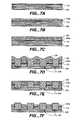
- FIGS. 7A-7Jare cross sections of memory array 100 at various stages during the fabrication process.
- FIG. 1Aillustrates a plan view of an embodiment of the NAND flash memory of the present invention.
- FIGS. 2-4are cross sections taken through the structure shown in FIG. 1 A.
- An electrical equivalent circuit of the memory arrayis given in FIG. 1B , wherein common elements within the structure of FIGS. 1 A and 2 - 4 are identified by the same reference character.
- Parallel wordlines 106connect adjacent NAND strings of floating gates 102 .
- the wordlines 106are illustrated horizontally, and the strings are illustrated vertically in the figures.
- a NAND stringgenerally includes a select gate followed by several floating gates and another select gate.
- the bitline A, B, and C (BL A , BL B , BL C ) locationscorrespond to the string locations in the plan view, although the bitlines are generally located in another plane.
- the circuit diagram of FIG. 1Bmost clearly shows the vertical array of strings. In this case sixteen floating gates and thus sixteen wordlines are illustrated per string, however, the number of floating gates may be thirty-two or more, and is foreseen to increase in the future.
- Floating gates 102are isolated from adjacent floating gates by isolation trenches 104 .
- Isolating trenches 104are also referred to as shallow trench isolation areas.
- the select gate line 105 on the source side (“SS”)is continuous between trenches 104 , as can be seen in section C—C of FIG. 4 . It is not etched into individual floating gates.
- SSsource side
- Metal bitlines 116connect to the N+ regions 114 within substrate 108 to sense amplifiers for reading the charge stored in the floating gates 102 .
- a stringis selected via the bitline and a wordline is also selected.
- the metal bitlinesare generally, but not necessarily, formed in a conductive layer insulated from the wordlines.
- At the end of each stringis another select gate coupled to the drain (“SD”).
- SDDrain
- the drain and sourcecan be interchanged in some configurations and more than 16 transistors can also be present in each string, thus also increasing the number of wordlines.
- gate oxide 112there is a portion of gate oxide 112 between each floating gate 102 and the substrate 108 .
- a dielectric material 110separates the wordlines 106 from the floating gates 102 and the isolation trenches 104 .
- Adjacent floating gates 102are isolated from other floating gates in the same wordline, not only by isolating trenches 104 , but also by wordlines 106 .
- Wordlines 106extend down between floating gates into isolation trenches 104 , until, within, or past the level of gate oxide layer 112 . This has several distinct benefits.
- the electrical field across the dielectric layer 110 between adjacent floating gatesis reduced, therefore reducing any leakage current through the dielectric layer that may occur as a result of the electrical field.
- the lesser the electrical fieldthe lesser the leakage current between two adjacent floating gates.
- the leakage current pathis greatly increased by the extended wordlines 106 . Any leakage current must travel down and around the extended portion of the wordlines and then back up or over to the adjacent floating gates.
- the charge level programmed onto a floating gate of a cellchanges when such a leakage current is present. Therefore, by minimizing the leakage current, and thus any change in charge of the floating gates, an increased number of levels can be discerned more reliably. This leads to a higher capacity, more cost efficient, and more reliable data storage system.
- the extended wordlineshields a selected floating gate from field effects of nearby channels.
- a floating gate that has been programmed with a particular chargemay, in a subsequent read or verify operation, indicate that it has a larger charge than it should due to a potential or charge in an adjacent channel. This is especially true with complicated program, read, and verify operations in multi-state NAND flash memory where multiple operations are occurring simultaneously in adjacent strings and cells.
- every other cell along one rowis part of the same page; in newer systems, every cell along one row can be part of the same page.
- floating gate 102 A activated by BL A and the floating gate 102 C activated by BL Cwould be programmed while the floating gate 102 B activated by BL B is not programmed.
- every cell along one rowcan be part of the same page.
- floating gate 102 A of the string activated by BL Amay be undergoing a programming operation at the same time as floating gate 102 B. This will be discussed in further detail later in reference to FIGS. 5D and 5E . In this way, twice the number of cells may be programmed and or verified at the same time. Although this may be efficient, it results in additional field effect problems during all of the various operations involved in data storage operations.
- an adjacent (substrate) channel of an adjacent cellmay be at a low potential, for instance 0V, for a number of programming pulses while it is being programmed and then suddenly be boosted or “locked out” for subsequent programming pulses to a high potential, for instance, 5, 7.5, or 10 V, after it verifies in order to stop further programming or for any other reason.
- This boosting of the channel potentialalso increases the floating gate potential of the adjacent cell.
- both the adjacent channel and adjacent floating gatewill couple a higher potential to the selected cell for the next programming pulse which may broaden the width of the programmed distribution.
- Thishas a number of negative consequences, some of which may include error in reading a particular bit and reduction in the total number of bits of data that may be stored in a given die size.
- FIGS. 5A-5EAn example of some programming details is illustrated in FIGS. 5A-5E which will be discussed below. The levels given are illustrative and only serve to educate the reader on the operation of an example memory system with which the present invention may be particularly advantageous.
- FIG. 5 AAn example of the incremental voltage steps of the programming pulses are shown in FIG. 5 A.
- the pulsesare incremented by 0.2 volts.
- After each pulsethere is a verify cycle, followed by an incrementally higher voltage pulse. This takes place until a desired or threshold voltage is verified in the floating gate. For example, this may take place until the floating gate is verified at 2.0 volts.
- FIG. 5Billustrates that for each program pulse, there is a distribution of the charge stored in the floating gates.
- the distribution of the verified chargesis about three volts. So, if it is desired to store 2.0 volts on the floating gate, it may be necessary to increment up to 17.0 volts and higher in the control gate or wordline. If, for example, after a 17.0 volt programming pulse the distribution of stored charges on the floating gates is such that there are some floating gates above and some below the 2.0 V threshold, those below will receive a further programming while those above the threshold will not by having their channel boosted or “locked out.”
- V tcell voltage
- some “fast” floating gatesmay reach the desired verify V t at a lower program voltage than other “slow” or “intermediate” floating gates.
- a cellhas a V t of 1.99 volts, it will receive another programming pulse to take it above the 2.0 volt threshold. In a constant environment, the cell should then have a V t of 2.19 volts. However, if there is any deviation of the voltage or electric field that is applied to the cell, for example between one programming pulse and another, the voltage stored on the cell may differ from that expected. If a neighboring component exerts an influence of the electrical field of the cell during a programming pulse, the charge stored will also deviate. For example, the cell that was at 1.99 volts in the previous verification cycle, may instead of having a V t of 2.19 volts may have a V t of 2.29 or 2.39 volts.
- the increase in the distribution of cellswill lessen the number of states that can be repeatably and reliably discerned in a multi-level storage system. This greatly lessens the storage capacity of a memory device with a given die size, and therefore increases the cost of production of a storage device with a desired storage capacity.
- an adjacent cellis any cell located near another cell, in any direction, including diagonally.
- floating gate 102 Ais adjacent to floating gate 102 B.
- the active area of the cellcomprises the channel area in the substrate below the floating gate and the wordline area above the floating gate.
- the cellmay also be said to comprise portions of the shallow trench isolation area and other components.
- a cellis “locked out” by isolating its corresponding bitline if it has verified at the desired program voltage. In the example given above, if the cell has verified at 2.0 volts, it will be “locked out” from further programming pulses by increasing the cell voltage in the channel (substrate) to a relatively high voltage level by isolating the corresponding bitline.
- FIG. 5Dshows an adjacent cell during the programming operations previously discussed.
- the shape and configuration of the cellsis simplified for ease of understanding.
- wordline 106 of the cellis at 18 volts
- floating gate 102is at 10 volts
- substrate 108is at 0 volts.
- wordline 106is now at 18.2 volts
- floating gate 102is now at 13 volts
- substrate 108is now at 8.0 volts.
- the channelis a portion of the substrate just below the upper surface of the substrate.
- an adjacent cellmay be either in the program operation shown in FIG. 5D , or the lockout state shown in FIG. 5 E.
- the voltages shown in the program operationsvary with the different programming pulses discussed earlier. All of these voltages shown in an adjacent cell may couple to a selected cell during programming. It is the variation in these voltages that may result in the variation from steady state programming ( FIG. 5C ) and thus increased deviation (FIG. 5 B).
- FIG. 6is a flowchart of the steps of making memory array 100 which should be referred to in tandem with FIGS. 7A-7J .
- the memory array 100is fabricated in a substrate 108 .
- Substrate 108preferably comprises silicon but may also comprise any material known to those in the art such as Gallium Arsenide etc. . . .
- a gate oxide layer 112is formed upon substrate 108 in step 505 as seen in FIG. 7 A.
- Gate oxide 112is preferably grown on substrate 108 but may also be deposited.
- Gate oxide layer 112preferably comprises silicon dioxide but may differ depending on what type of substrate is used and other processing factors or elements introduced during processing.
- gate oxide 112may comprise materials (known as ETO) including nitride/oxynitride.
- ETOnitride/oxynitride.
- a first gate layer 102 ais deposited upon gate oxide layer 112 in step 510 as seen in FIG. 7 B.
- the first gate layer 102 ais made of semiconducting material such as polysilicon.
- a nitride layer 120is then deposited upon the first floating gate layer 102 a in step 515 as seen in FIG 7 C.
- parallel trenchesare etched in substrate 108 with well known etching techniques. Generally in fabricating high density memory arrays where the features are of a very small scale, plasma etching is preferred over wet etching in order to have a precise and uniform etch.
- isolation trenches 104are then filled with a field oxide, as seen in FIG. 7D , to form isolation trenches 104 .
- the field oxide within isolation trenches 104is preferably comprised of silicon dioxide but can be comprised of other insulating materials (including materials other than oxides). Isolation trenches 104 range from about 0.2 microns to about 0.25 microns wide and are preferably about 0.2 microns wide.
- CMPchemical-mechanical polishing
- nitride layer 120is etched away such that isolation trenches 104 extend above the surface of the first gate layer 102 a, as seen in FIG 7 F.
- the isolating trenches 104may extend above the substrate 108 and gate oxide layer 112 as shown, or, alternatively, may only extend up to the level of either the substrate 108 , gate oxide layer 112 , or first gate layer 102 a, and it should be understood that differing processes and steps may be necessary to achieve these differing embodiments.
- a second gate layer 102 b of the same semiconducting material as the first gate layer 102 ais then deposited upon the gate oxide layer 112 and isolation trenches 104 in step 540 . It is then selectively etched above isolation trenches 104 to create floating gates 102 in step 545 .
- the resultant structurecan be seen in FIG. 7 G.
- Floating gates 102are substantially “T” shaped in order to maximize the coupling between the floating gate and the control gate, also referred to as the wordline 106 that activates the floating gate.
- the line between the first and second gate layers 102 a and 102 bhas been removed for the sake of clarity.
- the T shapeprovides a large surface area between floating gate and the wordline, thus maximizing the coupling ratio between the two devices for improved read, program and erase operations.
- U.S. patent application Ser. No. 09/925,102 to Yuan et al.entitled “Scalable Self-Aligned Dual Floating Gate Memory Cell Array and Methods of Forming the Array,” which is hereby incorporated by this reference in its entirety.
- a set of parallel trenches 122is formed within isolating trenches 104 in step 550 .
- Trenches 122may extend within trenches 104 to the level of the upper surface of gate oxide 112 or any distance within trenches 104 within or below the level of gate oxide 112 .
- Isolation layer 110is then deposited upon the floating gates 102 , and within second trenches 122 in isolation trenches 104 , in step 555 , as seen in FIG 7 I.
- Isolation layer 110is preferably a dielectric layer such as an oxide-nitride-oxide (“ONO”) layer 110 .
- the dielectric layer 110can be any type of dielectric known in the art and is not necessarily limited to an ONO structure.
- a wordline layercomprising a semiconducting material layer such as polysilicon and a conductive layer such as tungsten suicide is then deposited upon dielectric layer 110 in step 560 , as can be seen in FIG. 7 J.
- Wordlines 106are then etched from the wordline layer in step 565 .
- wordlines 106extend down between the floating gates 102 into the isolating trenches 104 . This isolates adjacent floating gates 102 from each other. In the preferred embodiment, wordlines 106 extend within the isolation trenches 104 to or beyond the level of the gate dielectric 112 .
- gate oxide layer 112may be formed before or after the parallel trenches are etched into substrate 108 etc. . . .
- additional layers, steps, and resultant structures that are not describedmay also be part of the process and the resultant memory array.
- the extended wordlinereduces the problem of the aforementioned Yupin effect because it acts as a shield between adjacent floating gates.
- the Yupin effectis when the charge stored or otherwise present in a neighboring cell influences the reading of a selected cell.
- the present solutionshields gates to avoid or minimize Yupin effect errors caused by neighboring gates. Yupin effect errors can also be accommodated through program and read circuitry and algorithms.
- the extended wordlinealso protects against conduction leakage between adjacent floating gates within the dielectric layer 110 because it blocks the conduction path between adjacent gates. Furthermore, any possible stringers as a result of an incomplete etch of the floating gate layer that might short circuit adjacent gates are also eliminated in the situation where the etch within the isolation trench extends past the upper (top of the “T”) portion of the T shaped floating gate.
- Yupin effect and on disturbsplease refer to U.S. Pat. No. 5,867,429, which was previously incorporated by reference.
Landscapes
- Semiconductor Memories (AREA)
- Non-Volatile Memory (AREA)
Abstract
Description
This application is a continuation-in-part of U.S. patent application Ser. No. 10/175,764, filed Jun. 19, 2002. This application is also related to U.S. Pat. No. 5,867,429 entitled “High Density Non-Volatile Flash Memory Without Adverse Effects of Electric Field Coupling Between Adjacent Floating Gates” which is hereby incorporated by this reference in its entirety.
1. Field of the Invention
This invention relates generally to flash electrically erasable and programmable read only memory (EEPROMS), and more specifically to NAND flash memory with a high memory cell density.
2. Related Art
Most existing commercial flash EEPROM products operate each memory cell with two ranges of threshold voltages, one above and the other below a breakpoint level, thereby defining two programmed states. One bit of data is thus stored in each cell, a 0 when programmed into one state and a 1 when programmed into its other state. A chunk of a given number of bits of data is programmed at one time into an equal number of cells. The state of each cell is monitored during programming so that application of programming voltages stops when the threshold level of an individual cell is verified to have moved within the range that represents the value of the bit of data being stored in the cell.
In order to increase the amount of data stored in a flash EEPROM system having a certain number of storage cells, the individual cells are operated with more than two threshold level states. Preferably, two or more bits of data are stored in each cell by operating the individual cells with four or more programmable states. Three threshold breakpoint levels are necessary to define four different threshold states. Such a system is described in U.S. Pat. Nos. 5,043,940 and 5,172,338, which are hereby incorporated by this reference in their entirety. In multi-state operation, an available operating voltage range of the individual cells is divided into an increased number of states. The use of eight or more states, resulting in storing three or more bits of data per cell, is contemplated. The voltage range of each state necessarily becomes smaller as the number of states is increased. This leaves less margin within each state to accommodate any error that might occur during operation of the memory system.
One type of error is termed a “disturb,” wherein electrons are unintentionally added to or taken away from a floating gate during operation of the memory. One source of a disturb is the presence of a leaky oxide dielectric positioned between the floating gate and another conductive gate of a cell. The charge level programmed onto a floating gate of a cell changes when such a leaky oxide is present, thus leading to the possibility that the state of the cell will be incorrectly read if the change in charge has been large enough. Since few to no errors can be tolerated in a mass digital data storage system, a sufficient margin for this error is provided by making the voltage range allocated to each state sufficient to include an expanded range of voltages that can occur as the result of such disturbs. This necessarily limits the number of states that can be included in a multi-state flash EEPROM system since the total available voltage range is limited.
Another type of error is termed the “Yupin effect.” The Yupin effect occurs when the neighboring cell of a selected cell is programmed after the selected cell itself is programmed, and the charges of the neighboring cell influence the voltage of the selected cell. Any potential present in an adjacent cell or string may influence the reading of a selected cell, including those in the channel, floating gate, or control gates etc. . . . Such interference from the subsequently programmed neighbor cell distorts the voltages of the selected cell, possibly leading to an erroneous identification of its memory state during reading.
The present invention is an improved structure for high density NAND type flash memory that minimizes the effect of disturbs and Yupin effect errors.
One aspect of the invention is a NAND flash memory device formed from a substrate. The device comprises strings of transistors. Each string has a first select gate, a plurality of floating gates, and a second select gate. The floating gates are formed between shallow trench isolation areas and wordlines extend across adjacent strings and extend between the floating gates into the shallow trench isolation areas thereby isolating adjacent floating gates. The wordlines shield a selected floating gate from the potentials, and from variations in the potentials of adjacent memory cells and components. The electric fields may emanate from a component located anywhere near the selected floating gate, for example above or below or at a diagonal.
Another aspect of the invention is a flash memory device formed from a substrate. The device comprises strings of adjacent transistors of a NAND architecture comprising a first select gate, a plurality of floating gates, and a second select gate, the plurality of floating gates formed above the substrate, wherein the strings are separated by shallow trench isolation areas. The device has two or more discrete programming levels programmed by increasing a programming potential until the levels are reached, wherein once the floating gates have reached a steady state a linear increase in programming potential results in an approximately linear increase in floating gate charge given a constant potential surrounding environment. Wordlines extend across adjacent strings and between the floating gates into the shallow trench isolation areas, such that when a floating gate of a selected string is read or verified, the wordline minimizes deviation from the linear increase due to voltage variations in the surrounding environment.
The present invention is better understood upon consideration of the detailed description below, in conjunction with the accompanying drawings of illustrative embodiments of the invention.
The following is a detailed description of illustrative embodiments of the present invention. As these embodiments of the present invention are described with reference to the aforementioned drawings, various modifications or adaptations of the methods and or specific structures described may become apparent to those skilled in the art. All such modifications, adaptations, or variations that rely upon the teachings of the present invention, and through which these teachings have advanced the art, are considered to be within the scope of the present invention. Hence, these descriptions and drawings are not to be considered in a limiting sense, as it is understood that the present invention is in no way limited to the embodiments illustrated.
Metal bitlines116 (only one of which is shown for the sake of clarity) connect to theN+ regions 114 withinsubstrate 108 to sense amplifiers for reading the charge stored in the floatinggates 102. Thus, to read a particular floating gate a string is selected via the bitline and a wordline is also selected. The metal bitlines are generally, but not necessarily, formed in a conductive layer insulated from the wordlines. At the end of each string is another select gate coupled to the drain (“SD”). The drain and source can be interchanged in some configurations and more than 16 transistors can also be present in each string, thus also increasing the number of wordlines.
As seen inFIG. 2 , there is a portion ofgate oxide 112 between each floatinggate 102 and thesubstrate 108. Adielectric material 110 separates thewordlines 106 from the floatinggates 102 and theisolation trenches 104. Adjacent floatinggates 102 are isolated from other floating gates in the same wordline, not only by isolatingtrenches 104, but also bywordlines 106.Wordlines 106 extend down between floating gates intoisolation trenches 104, until, within, or past the level ofgate oxide layer 112. This has several distinct benefits.
It reduces Yupin effects between adjacent cells in the wordline direction. Also, it improves the cell coupling ratio between the wordlines and the floating gates. The portion of the wordline that extends into the isolation trenches, to or past the depth of the floating gates, increases the overlap of the surface areas and volumes of the wordlines and floating gates. This increased overlap results in better coupling when a charge is read or stored during program, read, or erase operations.
The electrical field across thedielectric layer 110 between adjacent floating gates is reduced, therefore reducing any leakage current through the dielectric layer that may occur as a result of the electrical field. The lesser the electrical field, the lesser the leakage current between two adjacent floating gates. Additionally, the leakage current path is greatly increased by theextended wordlines 106. Any leakage current must travel down and around the extended portion of the wordlines and then back up or over to the adjacent floating gates. The charge level programmed onto a floating gate of a cell changes when such a leakage current is present. Therefore, by minimizing the leakage current, and thus any change in charge of the floating gates, an increased number of levels can be discerned more reliably. This leads to a higher capacity, more cost efficient, and more reliable data storage system.
Additionally, the extended wordline shields a selected floating gate from field effects of nearby channels. In certain program, read, and verify operations, a floating gate that has been programmed with a particular charge may, in a subsequent read or verify operation, indicate that it has a larger charge than it should due to a potential or charge in an adjacent channel. This is especially true with complicated program, read, and verify operations in multi-state NAND flash memory where multiple operations are occurring simultaneously in adjacent strings and cells. In many prior systems, every other cell along one row is part of the same page; in newer systems, every cell along one row can be part of the same page. Referring again toFIG. 2 , this would mean that in a prior system, the floatinggate 102A activated by BLAand the floatinggate 102C activated by BLCwould be programmed while the floatinggate 102B activated by BLBis not programmed. In newer systems, every cell along one row can be part of the same page. Thus, as seen inFIG. 2 , floatinggate 102A of the string activated by BLAmay be undergoing a programming operation at the same time as floatinggate 102B. This will be discussed in further detail later in reference toFIGS. 5D and 5E . In this way, twice the number of cells may be programmed and or verified at the same time. Although this may be efficient, it results in additional field effect problems during all of the various operations involved in data storage operations.
The relationship between the distribution and the incremental voltage of the programming pulses holds true only if the potential of any other coupling element to the floating gates of the cells being programmed remains constant. In the case of programming adjacent NAND strings, an adjacent (substrate) channel of an adjacent cell may be at a low potential, for instance 0V, for a number of programming pulses while it is being programmed and then suddenly be boosted or “locked out” for subsequent programming pulses to a high potential, for instance, 5, 7.5, or 10 V, after it verifies in order to stop further programming or for any other reason. This boosting of the channel potential also increases the floating gate potential of the adjacent cell. Thus, both the adjacent channel and adjacent floating gate will couple a higher potential to the selected cell for the next programming pulse which may broaden the width of the programmed distribution. This has a number of negative consequences, some of which may include error in reading a particular bit and reduction in the total number of bits of data that may be stored in a given die size. An example of some programming details is illustrated inFIGS. 5A-5E which will be discussed below. The levels given are illustrative and only serve to educate the reader on the operation of an example memory system with which the present invention may be particularly advantageous.
For further information regarding the data storage operations, please refer to U.S. patent application Ser. No. 09/893,277, filed Jun. 27, 2001, entitled “Operating Techniques For Reducing Effects Of Coupling Between Storage Elements Of A Non-Volatile Memory Operated In Multiple Data States,” hereby incorporated by this reference in its entirety, and an article entitled “Fast and Accurate Programming Method for Multi-level NAND EEPROMs”, pp. 129-130, Digest of1995Symposium of VLSI Technology, which is also hereby incorporated by this reference in its entirety, and discusses the timing and voltage levels of programming pulses using in the read/verify and programming operations.
An example of the incremental voltage steps of the programming pulses are shown in FIG.5A. In the example shown and described, the pulses are incremented by 0.2 volts. After each pulse, there is a verify cycle, followed by an incrementally higher voltage pulse. This takes place until a desired or threshold voltage is verified in the floating gate. For example, this may take place until the floating gate is verified at 2.0 volts.
With a constant environment, i.e. one where the potential and electric field of the neighboring components is constant, the programming pulses, will, after having reached a steady state, result in a predictable and approximately linear increase in the cell voltage (Vt), as seen in FIG.5C. As seen in the nearly parallel lines, some “fast” floating gates may reach the desired verify Vtat a lower program voltage than other “slow” or “intermediate” floating gates. Once the steady state has been reached, it can be seen that a linear increase in the program voltage results in a nearly linear increase in Vt.
Therefore, if, for example, a cell has a Vtof 1.99 volts, it will receive another programming pulse to take it above the 2.0 volt threshold. In a constant environment, the cell should then have a Vtof 2.19 volts. However, if there is any deviation of the voltage or electric field that is applied to the cell, for example between one programming pulse and another, the voltage stored on the cell may differ from that expected. If a neighboring component exerts an influence of the electrical field of the cell during a programming pulse, the charge stored will also deviate. For example, the cell that was at 1.99 volts in the previous verification cycle, may instead of having a Vtof 2.19 volts may have a Vtof 2.29 or 2.39 volts. As shown inFIG. 5C , coupling of potential from a nearby cell may cause one of the intermediate cells to deviate from the linear increase that is characteristic of the steady state. Thus, the distribution of the cells shown inFIG. 5B will increase due to any variation in the potential of adjacent components.
The increase in the distribution of cells will lessen the number of states that can be repeatably and reliably discerned in a multi-level storage system. This greatly lessens the storage capacity of a memory device with a given die size, and therefore increases the cost of production of a storage device with a desired storage capacity.
Specifically, as can be seen inFIGS. 5D and 5E , the voltages in the components of an adjacent cell will vary greatly during program and during “lockout.” An adjacent cell is any cell located near another cell, in any direction, including diagonally. For example, floatinggate 102A is adjacent to floatinggate 102B. The active area of the cell comprises the channel area in the substrate below the floating gate and the wordline area above the floating gate. The cell may also be said to comprise portions of the shallow trench isolation area and other components. A cell is “locked out” by isolating its corresponding bitline if it has verified at the desired program voltage. In the example given above, if the cell has verified at 2.0 volts, it will be “locked out” from further programming pulses by increasing the cell voltage in the channel (substrate) to a relatively high voltage level by isolating the corresponding bitline.
Next, instep 535,nitride layer 120 is etched away such thatisolation trenches 104 extend above the surface of thefirst gate layer 102a,as seen in FIG7F. The isolatingtrenches 104 may extend above thesubstrate 108 andgate oxide layer 112 as shown, or, alternatively, may only extend up to the level of either thesubstrate 108,gate oxide layer 112, orfirst gate layer 102a,and it should be understood that differing processes and steps may be necessary to achieve these differing embodiments.
Asecond gate layer 102bof the same semiconducting material as thefirst gate layer 102ais then deposited upon thegate oxide layer 112 andisolation trenches 104 instep 540. It is then selectively etched aboveisolation trenches 104 to create floatinggates 102 instep 545. The resultant structure can be seen in FIG.7G. Floatinggates 102 are substantially “T” shaped in order to maximize the coupling between the floating gate and the control gate, also referred to as thewordline 106 that activates the floating gate. The line between the first and second gate layers102aand102bhas been removed for the sake of clarity. The T shape provides a large surface area between floating gate and the wordline, thus maximizing the coupling ratio between the two devices for improved read, program and erase operations. For further information, please refer to co-pending U.S. patent application Ser. No. 09/925,102 to Yuan et al., entitled “Scalable Self-Aligned Dual Floating Gate Memory Cell Array and Methods of Forming the Array,” which is hereby incorporated by this reference in its entirety.
As seen inFIG. 7H , a set ofparallel trenches 122 is formed within isolatingtrenches 104 instep 550.Trenches 122 may extend withintrenches 104 to the level of the upper surface ofgate oxide 112 or any distance withintrenches 104 within or below the level ofgate oxide 112.Isolation layer 110 is then deposited upon the floatinggates 102, and withinsecond trenches 122 inisolation trenches 104, instep 555, as seen in FIG7I.Isolation layer 110 is preferably a dielectric layer such as an oxide-nitride-oxide (“ONO”)layer 110. Thedielectric layer 110 can be any type of dielectric known in the art and is not necessarily limited to an ONO structure. A wordline layer comprising a semiconducting material layer such as polysilicon and a conductive layer such as tungsten suicide is then deposited upondielectric layer 110 instep 560, as can be seen in FIG.7J.Wordlines 106 are then etched from the wordline layer instep 565.
As previously mentioned, thewordlines 106 extend down between the floatinggates 102 into the isolatingtrenches 104. This isolates adjacent floatinggates 102 from each other. In the preferred embodiment,wordlines 106 extend within theisolation trenches 104 to or beyond the level of thegate dielectric 112.
The various layers can be formed and the etching steps can be performed in many different well known methods and orders, and are not necessarily done in the order described, i.e.gate oxide layer 112 may be formed before or after the parallel trenches are etched intosubstrate 108 etc. . . . Furthermore, additional layers, steps, and resultant structures that are not described may also be part of the process and the resultant memory array.
The extended wordline reduces the problem of the aforementioned Yupin effect because it acts as a shield between adjacent floating gates. Again, in short, the Yupin effect is when the charge stored or otherwise present in a neighboring cell influences the reading of a selected cell. The present solution shields gates to avoid or minimize Yupin effect errors caused by neighboring gates. Yupin effect errors can also be accommodated through program and read circuitry and algorithms.
The extended wordline also protects against conduction leakage between adjacent floating gates within thedielectric layer 110 because it blocks the conduction path between adjacent gates. Furthermore, any possible stringers as a result of an incomplete etch of the floating gate layer that might short circuit adjacent gates are also eliminated in the situation where the etch within the isolation trench extends past the upper (top of the “T”) portion of the T shaped floating gate. For more information on the Yupin effect and on disturbs, please refer to U.S. Pat. No. 5,867,429, which was previously incorporated by reference.
While embodiments of the present invention have been shown and described, changes and modifications to these illustrative embodiments can be made without departing from the present invention in its broader aspects. Thus, it should be evident that there are other embodiments of this invention which, while not expressly described above, are within the scope of the present invention and therefore that the scope of the invention is not limited merely to the illustrative embodiments presented. Therefore, it will be understood that the appended claims set out the metes and bounds of the invention. However, as words are an imperfect way of describing the scope of the invention, it should also be understood that equivalent structures and methods while not within the express words of the claims are also within the true scope of the invention.
Claims (25)
1. A flash memory device formed from a substrate, the device comprising:
strings of adjacent transistors of a NAND architecture comprising a first select gate, a plurality of floating gates, and a second select gate, the plurality of floating gates formed above channel regions in the substrate and separated from the channel regions,
wherein adjacent first and second strings undergo programming operations at the same time, and wherein when programming a selected cell of the first string, any change in the potential in the second adjacent string is shielded from the first string by a wordline extending across adjacent strings and extending between the floating gates of the first and second strings into a shallow trench isolation area between the channel regions of adjacent strings to shield a floating gate of the first string from a potential of the second adjacent string.
2. The flash memory device ofclaim 1 wherein the wordline shields the floating gate of the first string from a potential in the substrate at an adjacent second string.
3. The flash memory device ofclaim 1 wherein the wordline shields the floating gate of the first string from a potential of the adjacent floating gate of the second string.
4. The flash memory device ofclaim 1 further comprising a gate oxide layer between the floating gates and the substrate, the wordline extending down past the level of an upper surface of the gate oxide layer.
5. The flash memory device ofclaim 1 wherein the wordline shields the floating gate of the first string from the potential of a floating gate of the second adjacent string.
6. A flash memory device comprising:
strings of adjacent transistors of a NAND architecture comprising a first select gate, a plurality of floating gates, and a second select gate, the plurality of floating gates formed above a substrate;
shallow trench isolation areas between the strings;
wordlines extending across adjacent strings and extending between the floating gates into the shallow trench isolation areas between the strings,
wherein in the case of programming adjacent NAND strings, a channel of a first string adjacent a floating gate of a second string is at a first potential for a number of programming pulses and changed to a second potential during subsequent programming pulses, and
wherein the potential of the channel of the first string couples to the potential of the floating gate of the second string, and
wherein the wordlines shield the floating gate of the second string from the potential of the channel of the first string.
7. The flash memory device ofclaim 6 further comprising a gate oxide layer between the floating gates and the substrate, the wordlines extending down past the level of an upper surface of the gate oxide layer.
8. The flash memory device ofclaim 6 wherein the wordlines extend down past the level of an upper surface of the substrate.
9. The flash memory device ofclaim 6 wherein the wordlines extend down past the lower level of the channel.
10. A flash memory device formed from a substrate, the device comprising:
strings of adjacent transistors of a NAND architecture comprising a first select gate, a plurality of floating gates, and a second select gate, the plurality of floating gates formed above the substrate,
the floating gates formed above a gate oxide layer formed upon cell channel regions within the substrate;
control gates that extend across adjacent strings and between the floating gates of adjacent strings, each control gate extending down past an upper surface of the substrate to shield a selected floating gate during a read or verify operation from a potential present in an adjacent string.
11. The flash memory device ofclaim 10 wherein the control gates shield the selected floating gate from the potential of the substrate beneath the adjacent string.
12. The flash memory device ofclaim 11 wherein the control gates shield the selected floating gate from the potential of a channel region of the substrate beneath the adjacent string.
13. The flash memory device ofclaim 10 wherein the control gates shield the selected floating gate from the potential of the floating gates of the adjacent string.
14. A flash memory device formed from a substrate, the device comprising:
strings of adjacent transistors of a NAND architecture comprising a first select gate, a plurality of floating gates, and a second select gate, the plurality of floating gates formed above the substrate, wherein the strings are separated by shallow trench isolation areas;
two or more discrete programming levels programmed by increasing a programming potential until the levels are reached, wherein once the floating gates have reached a steady state a linear increase in programming potential results in an approximately linear increase in floating gate charge given a constant potential surrounding environment; and
wordlines extending across adjacent strings and extending between the floating gates into the shallow trench isolation areas, such that when a floating gate of a selected string is read or verified, a wordline minimizes deviation from the linear increase due to voltage variations in the surrounding environment.
15. The flash memory device ofclaim 14 wherein the wordline shields the floating gate of the selected string from voltage variations in an adjacent portion of the substrate.
16. The flash memory device ofclaim 14 wherein the wordline shields the floating gate of the selected string from voltage variations in an adjacent floating gate.
17. The flash memory device ofclaim 14 wherein the wordline shields the floating gate of the first string from the potential of the channel region of the second adjacent string.
18. The flash memory device ofclaim 14 further comprising a gate oxide layer between the floating gates and the substrate, the wordline extending down past the level of an upper surface of the gate oxide layer.
19. The flash memory device ofclaim 14 wherein the wordline extends down past the level of an upper surface of the substrate.
20. A flash memory device comprising:
strings of adjacent transistors of a NAND architecture comprising a first select gate, a plurality of floating gates, and a second select gate, the plurality of floating gates formed above a substrate;
wherein in the case of programming adjacent NAND strings, a channel of a first string adjacent a floating gate of a second string is at a first potential for a number of programming pulses and changed to a second potential during subsequent programming pulses; and
means for controlling the floating gates and for isolating the floating gates from variations of adjacent potential fields during and between program pulses, the means for controlling the floating gates and for isolating the floating gates extending between the floating gates to or below the upper level of the substrate.
21. In a memory having a plurality of serious strings of memory cells arranged to form columns across a substrate surface and individually including a floating gate, wherein the strings of memory cells are separated by dielectric between them, and wherein a plurality of word lines extend across rows of memory cell floating gates the dielectric therebetween, a method of programming charge levels on an individual row of memory cells to defined states, comprising:
alternatively applying program pulses to and reading the states of memory cells along the row,
in response to reading that a memory cell along the row has reached its defined state, ceasing to apply any further programming pulses to such a memory cell while continuing to apply programming pulses to other memory cells in the row until all of the memory cells along the row have reached their defined states, and
utilizing isolation between the floating gates in the row during the alternate application of program pulses to and reading the state of the memory cells along the row by maintaining the word lines between adjacent floating gates and extending into the dielectric therebetween.
22. The method ofclaim 21 , wherein the dielectric fills trenches formed into the substrate surface between the column strings of memory cells, and providing isolation includes maintaining the word lines in the dielectric within the trenches to a level at least as low as the substrate surface.
23. The method ofclaim 22 , wherein providing isolation includes maintaining the word lines below the level of the substrate surface.
24. The method ofclaim 21 , wherein successive programming pulses are increased in magnitude.
25. The method ofclaim 21 , wherein the number of defined programmed states of the individual memory cells exceeds two.
Priority Applications (9)
| Application Number | Priority Date | Filing Date | Title |
|---|---|---|---|
| US10/353,570US6898121B2 (en) | 2002-06-19 | 2003-01-28 | Deep wordline trench to shield cross coupling between adjacent cells for scaled NAND |
| EP03736962.6AEP1514309B1 (en) | 2002-06-19 | 2003-06-09 | Deep wordline trench to shield cross coupling between adjacent cells of nand memory |
| PCT/US2003/018183WO2004001852A1 (en) | 2002-06-19 | 2003-06-09 | Deep wordline trench to shield cross coupling between adjacent cells for scaled nand |
| KR1020047020775AKR101110191B1 (en) | 2002-06-19 | 2003-06-09 | Deep wordline trench to shield cross coupling between adjacent cells for scaled nand |
| JP2004515756AJP4833547B2 (en) | 2002-06-19 | 2003-06-09 | Deep wordline trench for shielding cross coupling between adjacent cells for scaled NAND |
| CNB038139804ACN100340001C (en) | 2002-06-19 | 2003-06-09 | Deep wordline trench to shield cross coupling between adjacent cells for scaled NAND |
| AU2003237515AAU2003237515A1 (en) | 2002-06-19 | 2003-06-09 | Deep wordline trench to shield cross coupling between adjacent cells for scaled nand |
| US11/086,648US7170786B2 (en) | 2002-06-19 | 2005-03-21 | Deep wordline trench to shield cross coupling between adjacent cells for scaled NAND |
| US12/363,165USRE43417E1 (en) | 2002-06-19 | 2009-01-30 | Deep wordline trench to shield cross coupling between adjacent cells for scaled NAND |
Applications Claiming Priority (2)
| Application Number | Priority Date | Filing Date | Title |
|---|---|---|---|
| US10/175,764US6894930B2 (en) | 2002-06-19 | 2002-06-19 | Deep wordline trench to shield cross coupling between adjacent cells for scaled NAND |
| US10/353,570US6898121B2 (en) | 2002-06-19 | 2003-01-28 | Deep wordline trench to shield cross coupling between adjacent cells for scaled NAND |
Related Parent Applications (1)
| Application Number | Title | Priority Date | Filing Date |
|---|---|---|---|
| US10/175,764Continuation-In-PartUS6894930B2 (en) | 2002-06-19 | 2002-06-19 | Deep wordline trench to shield cross coupling between adjacent cells for scaled NAND |
Related Child Applications (1)
| Application Number | Title | Priority Date | Filing Date |
|---|---|---|---|
| US11/086,648ContinuationUS7170786B2 (en) | 2002-06-19 | 2005-03-21 | Deep wordline trench to shield cross coupling between adjacent cells for scaled NAND |
Publications (2)
| Publication Number | Publication Date |
|---|---|
| US20040012998A1 US20040012998A1 (en) | 2004-01-22 |
| US6898121B2true US6898121B2 (en) | 2005-05-24 |
Family
ID=29733973
Family Applications (3)
| Application Number | Title | Priority Date | Filing Date |
|---|---|---|---|
| US10/175,764Expired - LifetimeUS6894930B2 (en) | 2002-06-19 | 2002-06-19 | Deep wordline trench to shield cross coupling between adjacent cells for scaled NAND |
| US10/353,570Expired - LifetimeUS6898121B2 (en) | 2002-06-19 | 2003-01-28 | Deep wordline trench to shield cross coupling between adjacent cells for scaled NAND |
| US12/363,165Expired - LifetimeUSRE43417E1 (en) | 2002-06-19 | 2009-01-30 | Deep wordline trench to shield cross coupling between adjacent cells for scaled NAND |
Family Applications Before (1)
| Application Number | Title | Priority Date | Filing Date |
|---|---|---|---|
| US10/175,764Expired - LifetimeUS6894930B2 (en) | 2002-06-19 | 2002-06-19 | Deep wordline trench to shield cross coupling between adjacent cells for scaled NAND |
Family Applications After (1)
| Application Number | Title | Priority Date | Filing Date |
|---|---|---|---|
| US12/363,165Expired - LifetimeUSRE43417E1 (en) | 2002-06-19 | 2009-01-30 | Deep wordline trench to shield cross coupling between adjacent cells for scaled NAND |
Country Status (2)
| Country | Link |
|---|---|
| US (3) | US6894930B2 (en) |
| JP (1) | JP4833547B2 (en) |
Cited By (47)
| Publication number | Priority date | Publication date | Assignee | Title |
|---|---|---|---|---|
| US20050047261A1 (en)* | 2003-08-28 | 2005-03-03 | Naoki Kai | Nonvolatile semiconductor memory device having trench-type isolation region, and method of fabricating the same |
| US20050199939A1 (en)* | 2004-03-12 | 2005-09-15 | Lutze Jeffrey W. | Self aligned non-volatile memory cells and processes for fabrication |
| US20060176736A1 (en)* | 2002-10-28 | 2006-08-10 | Eliyahou Harari | Flash Memory Cell Arrays Having Dual Control Gates Per Memory Cell Charge Storage Element |
| US20060202263A1 (en)* | 2005-03-14 | 2006-09-14 | Chang-Hyun Lee | Nonvolatile semiconductor memory device and method of fabricating the same |
| US20070087504A1 (en)* | 2005-10-18 | 2007-04-19 | Pham Tuan D | Integration process flow for flash devices with low gap fill aspect ratio |
| US20070161191A1 (en)* | 2001-08-08 | 2007-07-12 | Yuan Jack H | Scalable Self-Aligned Dual Floating Gate Memory Cell Array And Methods Of Forming The Array |
| US20070243680A1 (en)* | 2006-04-13 | 2007-10-18 | Eliyahou Harari | Methods of Making Flash Memory Cell Arrays Having Dual Control Gates Per Memory Cell Charge Storage Element |
| US20090129159A1 (en)* | 2006-03-03 | 2009-05-21 | Nima Mokhlesi | Read operation for non-volatile storage with compensation for coupling |
| US20090201740A1 (en)* | 2008-01-09 | 2009-08-13 | Qimonda Ag | Integrated circuit, method to program a memory cell array of an integrated circuit, and memory module |
| US7745285B2 (en) | 2007-03-30 | 2010-06-29 | Sandisk Corporation | Methods of forming and operating NAND memory with side-tunneling |
| USRE43417E1 (en)* | 2002-06-19 | 2012-05-29 | SanDisk Technologies, Inc | Deep wordline trench to shield cross coupling between adjacent cells for scaled NAND |
| US8552771B1 (en) | 2012-05-29 | 2013-10-08 | Life Technologies Corporation | System for reducing noise in a chemical sensor array |
| US8692298B2 (en) | 2006-12-14 | 2014-04-08 | Life Technologies Corporation | Chemical sensor array having multiple sensors per well |
| US8731847B2 (en) | 2010-06-30 | 2014-05-20 | Life Technologies Corporation | Array configuration and readout scheme |
| US8742472B2 (en) | 2006-12-14 | 2014-06-03 | Life Technologies Corporation | Chemically sensitive sensors with sample and hold capacitors |
| US8841217B1 (en) | 2013-03-13 | 2014-09-23 | Life Technologies Corporation | Chemical sensor with protruded sensor surface |
| US8912580B2 (en) | 2009-05-29 | 2014-12-16 | Life Technologies Corporation | Active chemically-sensitive sensors with in-sensor current sources |
| US8912005B1 (en) | 2010-09-24 | 2014-12-16 | Life Technologies Corporation | Method and system for delta double sampling |
| US20140369127A1 (en)* | 2013-06-12 | 2014-12-18 | Kabushiki Kaisha Toshiba | Semiconductor memory device |
| US8962366B2 (en) | 2013-01-28 | 2015-02-24 | Life Technologies Corporation | Self-aligned well structures for low-noise chemical sensors |
| US8963216B2 (en) | 2013-03-13 | 2015-02-24 | Life Technologies Corporation | Chemical sensor with sidewall spacer sensor surface |
| US9116117B2 (en) | 2013-03-15 | 2015-08-25 | Life Technologies Corporation | Chemical sensor with sidewall sensor surface |
| US9128044B2 (en) | 2013-03-15 | 2015-09-08 | Life Technologies Corporation | Chemical sensors with consistent sensor surface areas |
| US9194000B2 (en) | 2008-06-25 | 2015-11-24 | Life Technologies Corporation | Methods and apparatus for measuring analytes using large scale FET arrays |
| US9239313B2 (en) | 2010-06-30 | 2016-01-19 | Life Technologies Corporation | Ion-sensing charge-accumulation circuits and methods |
| US20160181435A1 (en)* | 2014-12-22 | 2016-06-23 | Wafertech, Llc | Floating gate transistors and method for forming the same |
| US9404920B2 (en) | 2006-12-14 | 2016-08-02 | Life Technologies Corporation | Methods and apparatus for detecting molecular interactions using FET arrays |
| US20170069643A1 (en)* | 2004-08-19 | 2017-03-09 | Kabushiki Kaisha Toshiba | High-voltage transistor having shielding gate |
| US9618475B2 (en) | 2010-09-15 | 2017-04-11 | Life Technologies Corporation | Methods and apparatus for measuring analytes |
| US9671363B2 (en) | 2013-03-15 | 2017-06-06 | Life Technologies Corporation | Chemical sensor with consistent sensor surface areas |
| US9823217B2 (en) | 2013-03-15 | 2017-11-21 | Life Technologies Corporation | Chemical device with thin conductive element |
| US9835585B2 (en) | 2013-03-15 | 2017-12-05 | Life Technologies Corporation | Chemical sensor with protruded sensor surface |
| US9841398B2 (en) | 2013-01-08 | 2017-12-12 | Life Technologies Corporation | Methods for manufacturing well structures for low-noise chemical sensors |
| US9852919B2 (en) | 2013-01-04 | 2017-12-26 | Life Technologies Corporation | Methods and systems for point of use removal of sacrificial material |
| US9927393B2 (en) | 2009-05-29 | 2018-03-27 | Life Technologies Corporation | Methods and apparatus for measuring analytes |
| US9944981B2 (en) | 2008-10-22 | 2018-04-17 | Life Technologies Corporation | Methods and apparatus for measuring analytes |
| US9960253B2 (en) | 2010-07-03 | 2018-05-01 | Life Technologies Corporation | Chemically sensitive sensor with lightly doped drains |
| US9970984B2 (en) | 2011-12-01 | 2018-05-15 | Life Technologies Corporation | Method and apparatus for identifying defects in a chemical sensor array |
| US10077472B2 (en) | 2014-12-18 | 2018-09-18 | Life Technologies Corporation | High data rate integrated circuit with power management |
| US10100357B2 (en) | 2013-05-09 | 2018-10-16 | Life Technologies Corporation | Windowed sequencing |
| US10379079B2 (en) | 2014-12-18 | 2019-08-13 | Life Technologies Corporation | Methods and apparatus for measuring analytes using large scale FET arrays |
| US10451585B2 (en) | 2009-05-29 | 2019-10-22 | Life Technologies Corporation | Methods and apparatus for measuring analytes |
| US10458942B2 (en) | 2013-06-10 | 2019-10-29 | Life Technologies Corporation | Chemical sensor array having multiple sensors per well |
| US10605767B2 (en) | 2014-12-18 | 2020-03-31 | Life Technologies Corporation | High data rate integrated circuit with transmitter configuration |
| US11231451B2 (en) | 2010-06-30 | 2022-01-25 | Life Technologies Corporation | Methods and apparatus for testing ISFET arrays |
| US11307166B2 (en) | 2010-07-01 | 2022-04-19 | Life Technologies Corporation | Column ADC |
| US11339430B2 (en) | 2007-07-10 | 2022-05-24 | Life Technologies Corporation | Methods and apparatus for measuring analytes using large scale FET arrays |
Families Citing this family (52)
| Publication number | Priority date | Publication date | Assignee | Title |
|---|---|---|---|---|
| US6908817B2 (en)* | 2002-10-09 | 2005-06-21 | Sandisk Corporation | Flash memory array with increased coupling between floating and control gates |
| JP2005085996A (en)* | 2003-09-09 | 2005-03-31 | Toshiba Corp | Semiconductor device and manufacturing method thereof |
| US7221008B2 (en) | 2003-10-06 | 2007-05-22 | Sandisk Corporation | Bitline direction shielding to avoid cross coupling between adjacent cells for NAND flash memory |
| US7355237B2 (en)* | 2004-02-13 | 2008-04-08 | Sandisk Corporation | Shield plate for limiting cross coupling between floating gates |
| US7020017B2 (en)* | 2004-04-06 | 2006-03-28 | Sandisk Corporation | Variable programming of non-volatile memory |
| US8536661B1 (en) | 2004-06-25 | 2013-09-17 | University Of Hawaii | Biosensor chip sensor protection methods |
| US7212435B2 (en)* | 2004-06-30 | 2007-05-01 | Micron Technology, Inc. | Minimizing adjacent wordline disturb in a memory device |
| US7164168B2 (en)* | 2004-08-03 | 2007-01-16 | Micron Technology, Inc. | Non-planar flash memory having shielding between floating gates |
| US7388251B2 (en)* | 2004-08-11 | 2008-06-17 | Micron Technology, Inc. | Non-planar flash memory array with shielded floating gates on silicon mesas |
| WO2007008246A2 (en) | 2004-11-12 | 2007-01-18 | The Board Of Trustees Of The Leland Stanford Junior University | Charge perturbation detection system for dna and other molecules |
| US7381615B2 (en)* | 2004-11-23 | 2008-06-03 | Sandisk Corporation | Methods for self-aligned trench filling with grown dielectric for high coupling ratio in semiconductor devices |
| US7416956B2 (en)* | 2004-11-23 | 2008-08-26 | Sandisk Corporation | Self-aligned trench filling for narrow gap isolation regions |
| KR100630725B1 (en)* | 2004-12-17 | 2006-10-02 | 삼성전자주식회사 | Semiconductor device having buried bit line and manufacturing method thereof |
| US7202125B2 (en) | 2004-12-22 | 2007-04-10 | Sandisk Corporation | Low-voltage, multiple thin-gate oxide and low-resistance gate electrode |
| US7482223B2 (en) | 2004-12-22 | 2009-01-27 | Sandisk Corporation | Multi-thickness dielectric for semiconductor memory |
| TWI270199B (en)* | 2005-01-31 | 2007-01-01 | Powerchip Semiconductor Corp | Non-volatile memory and manufacturing method and operating method thereof |
| US20070106842A1 (en)* | 2005-11-04 | 2007-05-10 | Conley Kevin M | Enhanced first level storage caching methods using nonvolatile memory |
| US7634585B2 (en)* | 2005-11-04 | 2009-12-15 | Sandisk Corporation | In-line cache using nonvolatile memory between host and disk device |
| EP1786036A1 (en)* | 2005-11-11 | 2007-05-16 | STMicroelectronics S.r.l. | Floating gate non-volatile memory cell and process for manufacturing |
| US7436733B2 (en)* | 2006-03-03 | 2008-10-14 | Sandisk Corporation | System for performing read operation on non-volatile storage with compensation for coupling |
| US7499326B2 (en) | 2006-04-12 | 2009-03-03 | Sandisk Corporation | Apparatus for reducing the impact of program disturb |
| US7436713B2 (en) | 2006-04-12 | 2008-10-14 | Sandisk Corporation | Reducing the impact of program disturb |
| US7515463B2 (en) | 2006-04-12 | 2009-04-07 | Sandisk Corporation | Reducing the impact of program disturb during read |
| US7426137B2 (en) | 2006-04-12 | 2008-09-16 | Sandisk Corporation | Apparatus for reducing the impact of program disturb during read |
| US7440331B2 (en) | 2006-06-01 | 2008-10-21 | Sandisk Corporation | Verify operation for non-volatile storage using different voltages |
| US7457163B2 (en) | 2006-06-01 | 2008-11-25 | Sandisk Corporation | System for verifying non-volatile storage using different voltages |
| US7450421B2 (en)* | 2006-06-02 | 2008-11-11 | Sandisk Corporation | Data pattern sensitivity compensation using different voltage |
| US7310272B1 (en)* | 2006-06-02 | 2007-12-18 | Sandisk Corporation | System for performing data pattern sensitivity compensation using different voltage |
| US7440324B2 (en)* | 2006-12-29 | 2008-10-21 | Sandisk Corporation | Apparatus with alternating read mode |
| US7590002B2 (en)* | 2006-12-29 | 2009-09-15 | Sandisk Corporation | Resistance sensing and compensation for non-volatile storage |
| US7616498B2 (en)* | 2006-12-29 | 2009-11-10 | Sandisk Corporation | Non-volatile storage system with resistance sensing and compensation |
| US7495962B2 (en)* | 2006-12-29 | 2009-02-24 | Sandisk Corporation | Alternating read mode |
| US7535764B2 (en)* | 2007-03-21 | 2009-05-19 | Sandisk Corporation | Adjusting resistance of non-volatile memory using dummy memory cells |
| KR100900232B1 (en)* | 2007-05-22 | 2009-05-29 | 주식회사 하이닉스반도체 | Semiconductor device and manufacturing method thereof |
| US7636260B2 (en)* | 2007-06-25 | 2009-12-22 | Sandisk Corporation | Method for operating non-volatile storage with individually controllable shield plates between storage elements |
| US7781286B2 (en)* | 2007-06-25 | 2010-08-24 | Sandisk Corporation | Method for fabricating non-volatile storage with individually controllable shield plates between storage elements |
| US7808826B2 (en)* | 2007-06-25 | 2010-10-05 | Sandisk Corporation | Non-volatile storage with individually controllable shield plates between storage elements |
| US7869273B2 (en)* | 2007-09-04 | 2011-01-11 | Sandisk Corporation | Reducing the impact of interference during programming |
| JP2009283488A (en) | 2008-05-19 | 2009-12-03 | Toshiba Corp | Nonvolatile memory, and manufacturing method thereof |
| JP5491705B2 (en)* | 2008-05-22 | 2014-05-14 | 株式会社東芝 | Semiconductor device |
| US7893519B2 (en)* | 2008-05-28 | 2011-02-22 | Qimonda Ag | Integrated circuit with conductive structures |
| US8673627B2 (en) | 2009-05-29 | 2014-03-18 | Life Technologies Corporation | Apparatus and methods for performing electrochemical reactions |
| JP2011035268A (en)* | 2009-08-04 | 2011-02-17 | Toshiba Corp | Semiconductor memory device, and method of manufacturing the same |
| JP2012069203A (en) | 2010-09-22 | 2012-04-05 | Toshiba Corp | Nonvolatile semiconductor memory device and driving method for nonvolatile semiconductor memory device |
| JP2012069193A (en) | 2010-09-22 | 2012-04-05 | Toshiba Corp | Nonvolatile semiconductor memory device and its control method |
| US8916920B2 (en)* | 2011-07-19 | 2014-12-23 | Macronix International Co., Ltd. | Memory structure with planar upper surface |
| US8821798B2 (en) | 2012-01-19 | 2014-09-02 | Life Technologies Corporation | Titanium nitride as sensing layer for microwell structure |
| US8747748B2 (en) | 2012-01-19 | 2014-06-10 | Life Technologies Corporation | Chemical sensor with conductive cup-shaped sensor surface |
| US9099196B2 (en) | 2013-01-25 | 2015-08-04 | Samsung Electronics Co., Ltd. | Semiconductor memory device and method of operating the same |
| US8942043B2 (en) | 2013-03-04 | 2015-01-27 | Sandisk Technologies Inc. | Non-volatile storage with process that reduces read disturb on end wordlines |
| KR20170073980A (en)* | 2015-12-21 | 2017-06-29 | 에스케이하이닉스 주식회사 | Semiconductor memory device and operating method thereof |
| US9865609B2 (en)* | 2016-01-28 | 2018-01-09 | Taiwan Semiconductor Manufacturing Co., Ltd. | One-time-programming (OTP) memory cell with floating gate shielding |
Citations (47)
| Publication number | Priority date | Publication date | Assignee | Title |
|---|---|---|---|---|
| US5043940A (en) | 1988-06-08 | 1991-08-27 | Eliyahou Harari | Flash EEPROM memory systems having multistate storage cells |
| US5070032A (en) | 1989-03-15 | 1991-12-03 | Sundisk Corporation | Method of making dense flash eeprom semiconductor memory structures |
| US5095344A (en) | 1988-06-08 | 1992-03-10 | Eliyahou Harari | Highly compact eprom and flash eeprom devices |
| US5168465A (en) | 1988-06-08 | 1992-12-01 | Eliyahou Harari | Highly compact EPROM and flash EEPROM devices |
| US5172338A (en) | 1989-04-13 | 1992-12-15 | Sundisk Corporation | Multi-state EEprom read and write circuits and techniques |
| US5198380A (en) | 1988-06-08 | 1993-03-30 | Sundisk Corporation | Method of highly compact EPROM and flash EEPROM devices |
| US5268318A (en) | 1988-06-08 | 1993-12-07 | Eliyahou Harari | Highly compact EPROM and flash EEPROM devices |
| US5268319A (en) | 1988-06-08 | 1993-12-07 | Eliyahou Harari | Highly compact EPROM and flash EEPROM devices |
| US5297148A (en) | 1989-04-13 | 1994-03-22 | Sundisk Corporation | Flash eeprom system |
| US5313421A (en) | 1992-01-14 | 1994-05-17 | Sundisk Corporation | EEPROM with split gate source side injection |
| US5315541A (en) | 1992-07-24 | 1994-05-24 | Sundisk Corporation | Segmented column memory array |
| US5343063A (en) | 1990-12-18 | 1994-08-30 | Sundisk Corporation | Dense vertical programmable read only memory cell structure and processes for making them |
| US5471423A (en) | 1993-05-17 | 1995-11-28 | Nippon Steel Corporation | Non-volatile semiconductor memory device |
| US5512505A (en) | 1990-12-18 | 1996-04-30 | Sandisk Corporation | Method of making dense vertical programmable read only memory cell structure |
| US5534456A (en) | 1994-05-25 | 1996-07-09 | Sandisk Corporation | Method of making dense flash EEPROM cell array and peripheral supporting circuits formed in deposited field oxide with sidewall spacers |
| US5554563A (en) | 1995-04-04 | 1996-09-10 | Taiwan Semiconductor Manufacturing Company | In situ hot bake treatment that prevents precipitate formation after a contact layer etch back step |
| US5579259A (en) | 1995-05-31 | 1996-11-26 | Sandisk Corporation | Low voltage erase of a flash EEPROM system having a common erase electrode for two individually erasable sectors |
| US5640032A (en) | 1994-09-09 | 1997-06-17 | Nippon Steel Corporation | Non-volatile semiconductor memory device with improved rewrite speed |
| US5712179A (en) | 1995-10-31 | 1998-01-27 | Sandisk Corporation | Method of making triple polysilicon flash EEPROM arrays having a separate erase gate for each row of floating gates |
| US5712180A (en) | 1992-01-14 | 1998-01-27 | Sundisk Corporation | EEPROM with split gate source side injection |
| US5756385A (en) | 1994-03-30 | 1998-05-26 | Sandisk Corporation | Dense flash EEPROM cell array and peripheral supporting circuits formed in deposited field oxide with the use of spacers |
| US5786988A (en) | 1996-07-02 | 1998-07-28 | Sandisk Corporation | Integrated circuit chips made bendable by forming indentations in their back surfaces flexible packages thereof and methods of manufacture |
| US5867429A (en) | 1997-11-19 | 1999-02-02 | Sandisk Corporation | High density non-volatile flash memory without adverse effects of electric field coupling between adjacent floating gates |
| US5999448A (en) | 1998-03-17 | 1999-12-07 | Fujitsu Limited | Nonvolatile semiconductor memory device and method of reproducing data of nonvolatile semiconductor memory device |
| US6046935A (en) | 1996-03-18 | 2000-04-04 | Kabushiki Kaisha Toshiba | Semiconductor device and memory system |
| US6103573A (en) | 1999-06-30 | 2000-08-15 | Sandisk Corporation | Processing techniques for making a dual floating gate EEPROM cell array |
| US6151248A (en) | 1999-06-30 | 2000-11-21 | Sandisk Corporation | Dual floating gate EEPROM cell array with steering gates shared by adjacent cells |
| US6180457B1 (en) | 1998-09-25 | 2001-01-30 | Samsung Electronics Co., Ltd. | Method of manufacturing non-volatile memory device |
| US6208545B1 (en) | 1997-04-04 | 2001-03-27 | Glenn J. Leedy | Three dimensional structure memory |
| US6222762B1 (en) | 1992-01-14 | 2001-04-24 | Sandisk Corporation | Multi-state memory |
| US6235586B1 (en) | 1999-07-13 | 2001-05-22 | Advanced Micro Devices, Inc. | Thin floating gate and conductive select gate in situ doped amorphous silicon material for NAND type flash memory device applications |
| US20010001491A1 (en) | 1997-11-07 | 2001-05-24 | Koji Sakui | Semiconductor memory device having memory cells each having a conductive body of booster plate and a method for manufacturing the same |
| US6258665B1 (en) | 1997-03-21 | 2001-07-10 | Kabushiki Kaisha Toshiba | Non-volatile semiconductor memory device and method for manufacturing the same |
| US6281075B1 (en) | 1999-01-27 | 2001-08-28 | Sandisk Corporation | Method of controlling of floating gate oxide growth by use of an oxygen barrier |
| US6295227B1 (en)* | 1998-11-26 | 2001-09-25 | Kabushiki Kaisha Toshiba | Non-volatile semiconductor memory device |
| US6391717B1 (en) | 1999-12-28 | 2002-05-21 | Hyundai Electronics Industries Co., Ltd. | Method of manufacturing a flash memory device |
| US6403421B1 (en) | 1998-04-22 | 2002-06-11 | Sony Corporation | Semiconductor nonvolatile memory device and method of producing the same |
| US6417538B1 (en) | 1998-07-23 | 2002-07-09 | Samsung Electronics Co., Ltd. | Nonvolative semiconductor memory device with high impurity concentration under field oxide layer |
| US20020093073A1 (en) | 2000-10-30 | 2002-07-18 | Kabushiki Kaisha Toshiba | Semiconductor device having two-layered charge storage electrode |
| KR20020088554A (en) | 2001-05-18 | 2002-11-29 | 삼성전자 주식회사 | Flash Memory Cell and Method Of Forming The Same |
| US6512263B1 (en) | 2000-09-22 | 2003-01-28 | Sandisk Corporation | Non-volatile memory cell array having discontinuous source and drain diffusions contacted by continuous bit line conductors and methods of forming |
| US6529410B1 (en)* | 2000-09-20 | 2003-03-04 | Advanced Micro Devices, Inc. | NAND array structure and method with buried layer |
| US6614684B1 (en) | 1999-02-01 | 2003-09-02 | Hitachi, Ltd. | Semiconductor integrated circuit and nonvolatile memory element |
| US6624464B2 (en) | 2000-11-14 | 2003-09-23 | Samsung Electronics Co., Ltd. | Highly integrated non-volatile memory cell array having a high program speed |
| US6762092B2 (en) | 2001-08-08 | 2004-07-13 | Sandisk Corporation | Scalable self-aligned dual floating gate memory cell array and methods of forming the array |
| US6770932B2 (en) | 2002-07-10 | 2004-08-03 | Kabushiki Kaisha Toshiba | Semiconductor memory device having a memory region and a peripheral region, and a manufacturing method thereof |
| US6807095B2 (en)* | 2001-06-27 | 2004-10-19 | Sandisk Corporation | Multi-state nonvolatile memory capable of reducing effects of coupling between storage elements |
Family Cites Families (55)
| Publication number | Priority date | Publication date | Assignee | Title |
|---|---|---|---|---|
| US93073A (en)* | 1869-07-27 | Improvement in valves for hydraulic presses | ||
| US5053839A (en)* | 1990-01-23 | 1991-10-01 | Texas Instruments Incorporated | Floating gate memory cell and device |
| IT1243303B (en) | 1990-07-24 | 1994-05-26 | Sgs Thomson Microelectronics | DEPLOYING OF MEMORY CELLS WITH METAL LINES OF SOURCE AND DRAIN CONNECTION FORMED ON THE SUBSTRATE AND ORTHOGONALLY OVERLAYED BY LINES OF GATE CONNECTION AND PROCEDURE FOR ITS MANUFACTURE |
| US20080079059A1 (en) | 1991-04-24 | 2008-04-03 | Eon Silicon Solution Inc. | Method of manufacturing a nonvolatile semiconductor memory device and select gate device having a stacked gate structure |
| JP2750986B2 (en) | 1992-10-27 | 1998-05-18 | 尚茂 玉蟲 | Insulated gate electrostatic induction thyristor with split gate type cathode short circuit structure |
| DE69427532T2 (en) | 1994-02-17 | 2002-04-18 | National Semiconductor Corp., Sunnyvale | METHOD FOR REDUCING THE DISTANCE BETWEEN THE HORIZONTAL NEXT FLOATING GATES OF A FLASH EPROM ARRANGEMENT |
| US5680347A (en)* | 1994-06-29 | 1997-10-21 | Kabushiki Kaisha Toshiba | Nonvolatile semiconductor memory device |
| JP3469362B2 (en) | 1994-08-31 | 2003-11-25 | 株式会社東芝 | Semiconductor storage device |
| US5498560A (en) | 1994-09-16 | 1996-03-12 | Motorola, Inc. | Process for forming an electrically programmable read-only memory cell |
| JP2655124B2 (en) | 1995-03-06 | 1997-09-17 | 日本電気株式会社 | Nonvolatile semiconductor memory device and method of manufacturing the same |
| US5680345A (en)* | 1995-06-06 | 1997-10-21 | Advanced Micro Devices, Inc. | Nonvolatile memory cell with vertical gate overlap and zero birds beaks |
| DE19525070C2 (en) | 1995-07-10 | 2001-12-06 | Infineon Technologies Ag | Electrically writable and erasable read-only memory cell arrangement and method for the production thereof |
| JP3366173B2 (en) | 1995-07-31 | 2003-01-14 | シャープ株式会社 | Manufacturing method of nonvolatile semiconductor memory |
| KR0179163B1 (en) | 1995-12-26 | 1999-03-20 | 문정환 | Method of manufacturing non-volatile memory cell |
| KR100192551B1 (en) | 1996-05-16 | 1999-06-15 | 구본준 | Semiconductor memory device and fabrication method of the same |
| US5751038A (en)* | 1996-11-26 | 1998-05-12 | Philips Electronics North America Corporation | Electrically erasable and programmable read only memory (EEPROM) having multiple overlapping metallization layers |
| JPH10320988A (en) | 1997-05-23 | 1998-12-04 | Sony Corp | Semiconductor non-volatile memory device, its data programming method and its manufacture |
| JP4330670B2 (en)* | 1997-06-06 | 2009-09-16 | 株式会社東芝 | Nonvolatile semiconductor memory device |
| US6342715B1 (en)* | 1997-06-27 | 2002-01-29 | Kabushiki Kaisha Toshiba | Nonvolatile semiconductor memory device |
| JP3602691B2 (en) | 1997-06-27 | 2004-12-15 | 株式会社東芝 | Nonvolatile semiconductor memory device and method of manufacturing the same |
| JP3583583B2 (en) | 1997-07-08 | 2004-11-04 | 株式会社東芝 | Semiconductor device and manufacturing method thereof |
| US5851881A (en) | 1997-10-06 | 1998-12-22 | Taiwan Semiconductor Manufacturing Company, Ltd. | Method of making monos flash memory for multi-level logic |
| US5981335A (en) | 1997-11-20 | 1999-11-09 | Vanguard International Semiconductor Corporation | Method of making stacked gate memory cell structure |
| JP3447939B2 (en) | 1997-12-10 | 2003-09-16 | 株式会社東芝 | Nonvolatile semiconductor memory and data reading method |
| JPH11186419A (en) | 1997-12-25 | 1999-07-09 | Toshiba Corp | Nonvolatile semiconductor memory device |
| US6069382A (en) | 1998-02-11 | 2000-05-30 | Cypress Semiconductor Corp. | Non-volatile memory cell having a high coupling ratio |
| WO1999044239A1 (en) | 1998-02-25 | 1999-09-02 | Siemens Aktiengesellschaft | Electrically programmable memory cell arrangement and method for producing the same |
| JP3298509B2 (en) | 1998-06-12 | 2002-07-02 | 日本電気株式会社 | Method for manufacturing semiconductor device |
| TW399288B (en) | 1998-12-24 | 2000-07-21 | United Microelectronics Corp | Structure of flash memory and the manufacturing method thereof |
| JP2000236031A (en)* | 1999-02-16 | 2000-08-29 | Toshiba Corp | Nonvolatile semiconductor memory device |
| US6256225B1 (en) | 1999-02-26 | 2001-07-03 | Micron Technology, Inc. | Construction and application for non-volatile reprogrammable switches |
| JP4273558B2 (en)* | 1999-03-17 | 2009-06-03 | ソニー株式会社 | Nonvolatile semiconductor memory device and erase verify method thereof |
| US6159801A (en) | 1999-04-26 | 2000-12-12 | Taiwan Semiconductor Manufacturing Company | Method to increase coupling ratio of source to floating gate in split-gate flash |
| JP2001015717A (en)* | 1999-06-30 | 2001-01-19 | Toshiba Corp | Nonvolatile semiconductor memory device |
| KR20010004990A (en) | 1999-06-30 | 2001-01-15 | 김영환 | Flash EEPROM cell and method of manufacturing the same |
| EP1104023A1 (en) | 1999-11-26 | 2001-05-30 | STMicroelectronics S.r.l. | Process for manufacturing electronic devices comprising non-volatile memory cells |
| US6518618B1 (en) | 1999-12-03 | 2003-02-11 | Intel Corporation | Integrated memory cell and method of fabrication |
| JP2001168306A (en) | 1999-12-09 | 2001-06-22 | Toshiba Corp | Nonvolatile semiconductor memory device and method of manufacturing the same |
| JP2002026151A (en) | 2000-07-05 | 2002-01-25 | Mitsubishi Electric Corp | Semiconductor memory device |
| TW457713B (en) | 2000-10-06 | 2001-10-01 | Winbond Electronics Corp | Manufacturing method of EEPROM cell |
| US6738289B2 (en) | 2001-02-26 | 2004-05-18 | Sandisk Corporation | Non-volatile memory with improved programming and method therefor |
| US6559009B2 (en) | 2001-03-29 | 2003-05-06 | Macronix International Co. Ltd. | Method of fabricating a high-coupling ratio flash memory |
| JP2002359308A (en) | 2001-06-01 | 2002-12-13 | Toshiba Corp | Semiconductor memory device and method of manufacturing the same |
| US6894930B2 (en)* | 2002-06-19 | 2005-05-17 | Sandisk Corporation | Deep wordline trench to shield cross coupling between adjacent cells for scaled NAND |
| KR101110191B1 (en) | 2002-06-19 | 2012-02-15 | 쌘디스크 코포레이션 | Deep wordline trench to shield cross coupling between adjacent cells for scaled nand |
| US6888755B2 (en) | 2002-10-28 | 2005-05-03 | Sandisk Corporation | Flash memory cell arrays having dual control gates per memory cell charge storage element |
| US6801095B2 (en) | 2002-11-26 | 2004-10-05 | Agere Systems, Inc. | Method, program and system for designing an interconnected multi-stage oscillator |
| JP3927156B2 (en) | 2003-02-26 | 2007-06-06 | 株式会社東芝 | Nonvolatile semiconductor memory device |
| JP4005962B2 (en) | 2003-09-22 | 2007-11-14 | 株式会社東芝 | Nonvolatile semiconductor memory device |
| US7154779B2 (en) | 2004-01-21 | 2006-12-26 | Sandisk Corporation | Non-volatile memory cell using high-k material inter-gate programming |
| US7355237B2 (en) | 2004-02-13 | 2008-04-08 | Sandisk Corporation | Shield plate for limiting cross coupling between floating gates |
| US7183153B2 (en) | 2004-03-12 | 2007-02-27 | Sandisk Corporation | Method of manufacturing self aligned non-volatile memory cells |
| ATE516311T1 (en) | 2004-10-12 | 2011-07-15 | Exxonmobil Chem Patents Inc | TRIALKYLALUMINUM TREATED SUPPORT |
| JP4521366B2 (en) | 2006-02-22 | 2010-08-11 | 株式会社東芝 | Nonvolatile semiconductor memory device and method for manufacturing nonvolatile semiconductor memory device |
| US7615445B2 (en) | 2006-09-21 | 2009-11-10 | Sandisk Corporation | Methods of reducing coupling between floating gates in nonvolatile memory |
- 2002
- 2002-06-19USUS10/175,764patent/US6894930B2/ennot_activeExpired - Lifetime
- 2003
- 2003-01-28USUS10/353,570patent/US6898121B2/ennot_activeExpired - Lifetime
- 2003-06-09JPJP2004515756Apatent/JP4833547B2/ennot_activeExpired - Fee Related
- 2009
- 2009-01-30USUS12/363,165patent/USRE43417E1/ennot_activeExpired - Lifetime
Patent Citations (58)
| Publication number | Priority date | Publication date | Assignee | Title |
|---|---|---|---|---|
| US5268318A (en) | 1988-06-08 | 1993-12-07 | Eliyahou Harari | Highly compact EPROM and flash EEPROM devices |
| US5268319A (en) | 1988-06-08 | 1993-12-07 | Eliyahou Harari | Highly compact EPROM and flash EEPROM devices |
| US5095344A (en) | 1988-06-08 | 1992-03-10 | Eliyahou Harari | Highly compact eprom and flash eeprom devices |
| US5168465A (en) | 1988-06-08 | 1992-12-01 | Eliyahou Harari | Highly compact EPROM and flash EEPROM devices |
| US5043940A (en) | 1988-06-08 | 1991-08-27 | Eliyahou Harari | Flash EEPROM memory systems having multistate storage cells |
| US5198380A (en) | 1988-06-08 | 1993-03-30 | Sundisk Corporation | Method of highly compact EPROM and flash EEPROM devices |
| US5070032A (en) | 1989-03-15 | 1991-12-03 | Sundisk Corporation | Method of making dense flash eeprom semiconductor memory structures |
| US5172338A (en) | 1989-04-13 | 1992-12-15 | Sundisk Corporation | Multi-state EEprom read and write circuits and techniques |
| US5172338B1 (en) | 1989-04-13 | 1997-07-08 | Sandisk Corp | Multi-state eeprom read and write circuits and techniques |
| US5297148A (en) | 1989-04-13 | 1994-03-22 | Sundisk Corporation | Flash eeprom system |
| US5965913A (en) | 1990-12-18 | 1999-10-12 | Sandisk Corporation | Dense vertical programmable read only memory cell structures and processes for making them |
| US5343063A (en) | 1990-12-18 | 1994-08-30 | Sundisk Corporation | Dense vertical programmable read only memory cell structure and processes for making them |
| US5380672A (en) | 1990-12-18 | 1995-01-10 | Sundisk Corporation | Dense vertical programmable read only memory cell structures and processes for making them |
| US5847425A (en) | 1990-12-18 | 1998-12-08 | Sandisk Corporation | Dense vertical programmable read only memory cell structures and processes for making them |
| US5512505A (en) | 1990-12-18 | 1996-04-30 | Sandisk Corporation | Method of making dense vertical programmable read only memory cell structure |
| US6222762B1 (en) | 1992-01-14 | 2001-04-24 | Sandisk Corporation | Multi-state memory |
| US5712180A (en) | 1992-01-14 | 1998-01-27 | Sundisk Corporation | EEPROM with split gate source side injection |
| US5883409A (en) | 1992-01-14 | 1999-03-16 | Sandisk Corporation | EEPROM with split gate source side injection |
| US5313421A (en) | 1992-01-14 | 1994-05-17 | Sundisk Corporation | EEPROM with split gate source side injection |
| US5315541A (en) | 1992-07-24 | 1994-05-24 | Sundisk Corporation | Segmented column memory array |
| US5471423A (en) | 1993-05-17 | 1995-11-28 | Nippon Steel Corporation | Non-volatile semiconductor memory device |
| US5756385A (en) | 1994-03-30 | 1998-05-26 | Sandisk Corporation | Dense flash EEPROM cell array and peripheral supporting circuits formed in deposited field oxide with the use of spacers |
| US5595924A (en) | 1994-05-25 | 1997-01-21 | Sandisk Corporation | Technique of forming over an irregular surface a polysilicon layer with a smooth surface |
| US5534456A (en) | 1994-05-25 | 1996-07-09 | Sandisk Corporation | Method of making dense flash EEPROM cell array and peripheral supporting circuits formed in deposited field oxide with sidewall spacers |
| US5654217A (en) | 1994-05-25 | 1997-08-05 | Sandisk Corporation | Dense flash EEPROM cell array and peripheral supporting circuits formed in deposited field oxide with the use of spacers |
| US5747359A (en) | 1994-05-25 | 1998-05-05 | Sandisk Corporation | Method of patterning polysilicon layers on substrate |
| US5661053A (en) | 1994-05-25 | 1997-08-26 | Sandisk Corporation | Method of making dense flash EEPROM cell array and peripheral supporting circuits formed in deposited field oxide with the use of spacers |
| US5640032A (en) | 1994-09-09 | 1997-06-17 | Nippon Steel Corporation | Non-volatile semiconductor memory device with improved rewrite speed |
| US5554563A (en) | 1995-04-04 | 1996-09-10 | Taiwan Semiconductor Manufacturing Company | In situ hot bake treatment that prevents precipitate formation after a contact layer etch back step |
| US5579259A (en) | 1995-05-31 | 1996-11-26 | Sandisk Corporation | Low voltage erase of a flash EEPROM system having a common erase electrode for two individually erasable sectors |
| US5677872A (en) | 1995-05-31 | 1997-10-14 | Sandisk Corporation | Low voltage erase of a flash EEPROM system having a common erase electrode for two individual erasable sectors |
| US5712179A (en) | 1995-10-31 | 1998-01-27 | Sandisk Corporation | Method of making triple polysilicon flash EEPROM arrays having a separate erase gate for each row of floating gates |
| US6028336A (en) | 1995-10-31 | 2000-02-22 | Sandisk Corporation | Triple polysilicon flash EEPROM arrays having a separate erase gate for each row of floating gates, and methods of manufacturing such arrays |
| US6046935A (en) | 1996-03-18 | 2000-04-04 | Kabushiki Kaisha Toshiba | Semiconductor device and memory system |
| US5786988A (en) | 1996-07-02 | 1998-07-28 | Sandisk Corporation | Integrated circuit chips made bendable by forming indentations in their back surfaces flexible packages thereof and methods of manufacture |
| US6258665B1 (en) | 1997-03-21 | 2001-07-10 | Kabushiki Kaisha Toshiba | Non-volatile semiconductor memory device and method for manufacturing the same |
| US6208545B1 (en) | 1997-04-04 | 2001-03-27 | Glenn J. Leedy | Three dimensional structure memory |
| US20010001491A1 (en) | 1997-11-07 | 2001-05-24 | Koji Sakui | Semiconductor memory device having memory cells each having a conductive body of booster plate and a method for manufacturing the same |
| US5867429A (en) | 1997-11-19 | 1999-02-02 | Sandisk Corporation | High density non-volatile flash memory without adverse effects of electric field coupling between adjacent floating gates |
| US5999448A (en) | 1998-03-17 | 1999-12-07 | Fujitsu Limited | Nonvolatile semiconductor memory device and method of reproducing data of nonvolatile semiconductor memory device |
| US6403421B1 (en) | 1998-04-22 | 2002-06-11 | Sony Corporation | Semiconductor nonvolatile memory device and method of producing the same |
| US6417538B1 (en) | 1998-07-23 | 2002-07-09 | Samsung Electronics Co., Ltd. | Nonvolative semiconductor memory device with high impurity concentration under field oxide layer |
| US6180457B1 (en) | 1998-09-25 | 2001-01-30 | Samsung Electronics Co., Ltd. | Method of manufacturing non-volatile memory device |
| US6295227B1 (en)* | 1998-11-26 | 2001-09-25 | Kabushiki Kaisha Toshiba | Non-volatile semiconductor memory device |
| US6281075B1 (en) | 1999-01-27 | 2001-08-28 | Sandisk Corporation | Method of controlling of floating gate oxide growth by use of an oxygen barrier |
| US6614684B1 (en) | 1999-02-01 | 2003-09-02 | Hitachi, Ltd. | Semiconductor integrated circuit and nonvolatile memory element |
| US6151248A (en) | 1999-06-30 | 2000-11-21 | Sandisk Corporation | Dual floating gate EEPROM cell array with steering gates shared by adjacent cells |
| US6103573A (en) | 1999-06-30 | 2000-08-15 | Sandisk Corporation | Processing techniques for making a dual floating gate EEPROM cell array |
| US6235586B1 (en) | 1999-07-13 | 2001-05-22 | Advanced Micro Devices, Inc. | Thin floating gate and conductive select gate in situ doped amorphous silicon material for NAND type flash memory device applications |
| US6391717B1 (en) | 1999-12-28 | 2002-05-21 | Hyundai Electronics Industries Co., Ltd. | Method of manufacturing a flash memory device |
| US6529410B1 (en)* | 2000-09-20 | 2003-03-04 | Advanced Micro Devices, Inc. | NAND array structure and method with buried layer |
| US6512263B1 (en) | 2000-09-22 | 2003-01-28 | Sandisk Corporation | Non-volatile memory cell array having discontinuous source and drain diffusions contacted by continuous bit line conductors and methods of forming |
| US20020093073A1 (en) | 2000-10-30 | 2002-07-18 | Kabushiki Kaisha Toshiba | Semiconductor device having two-layered charge storage electrode |
| US6624464B2 (en) | 2000-11-14 | 2003-09-23 | Samsung Electronics Co., Ltd. | Highly integrated non-volatile memory cell array having a high program speed |
| KR20020088554A (en) | 2001-05-18 | 2002-11-29 | 삼성전자 주식회사 | Flash Memory Cell and Method Of Forming The Same |
| US6807095B2 (en)* | 2001-06-27 | 2004-10-19 | Sandisk Corporation | Multi-state nonvolatile memory capable of reducing effects of coupling between storage elements |
| US6762092B2 (en) | 2001-08-08 | 2004-07-13 | Sandisk Corporation | Scalable self-aligned dual floating gate memory cell array and methods of forming the array |
| US6770932B2 (en) | 2002-07-10 | 2004-08-03 | Kabushiki Kaisha Toshiba | Semiconductor memory device having a memory region and a peripheral region, and a manufacturing method thereof |
Non-Patent Citations (7)
| Title |
|---|
| Aritome et al., "A Novel Side-Wall Transfer-Transistor Cell (SWATT Cell) For Multi-Level NAND EEPROMs", 1995 IEEE International Solid-State Circuits Conference, IEDM 95, pp. 275-278. |
| Aritome et al., "A0.67um2 Self-Aligned Shallow Trench Isolation Cell (SA-STI-CELL) for 3V-only 256Mbit NAND EEPROMs", IEDM Technical digest, pp. 61-64 (1994). |
| Cho et al., "A Dual-Mode NAND Flash Memory: 1-Gb Multilevel and High-Performance 512-Mb Single-Level Modes", IEEE Journal of Solid-State Circuits, vol. 36, No. 11, pp. 1700-1706 (2001). |
| International Search Report, PCT/US03/18183 filed Sep. 6, 2003. |
| Seiichi Aritome, "Advanced Flash Memory Technology and Trends for File Storage Application," 2000 International Electron Devices Meeting, Dec. 10-13, 2000, pp. 33.1.1-33.1.4. |
| U.S. patent application Ser. No. 09/925,102, Yuan, filed Aug. 8, 2001. |
| Y. Takeuchi et al., "A Self-Aligned STI Process Integration for Low Cost and Highly Reliable 1Gbit Flash Memories," 1998 Symposium on VLSI Technology-Digest of Technical Papers, Jun. 9-11, 1998, pp. 102. |
Cited By (134)
| Publication number | Priority date | Publication date | Assignee | Title |
|---|---|---|---|---|
| US7858472B2 (en) | 2001-08-08 | 2010-12-28 | Sandisk Corporation | Scalable self-aligned dual floating gate memory cell array and methods of forming the array |
| US20070161191A1 (en)* | 2001-08-08 | 2007-07-12 | Yuan Jack H | Scalable Self-Aligned Dual Floating Gate Memory Cell Array And Methods Of Forming The Array |
| USRE43417E1 (en)* | 2002-06-19 | 2012-05-29 | SanDisk Technologies, Inc | Deep wordline trench to shield cross coupling between adjacent cells for scaled NAND |
| US20100047982A1 (en)* | 2002-10-28 | 2010-02-25 | Eliyahou Harari | Flash Memory Cell Arrays Having Dual Control Gates Per Memory Cell Charge Storage Element |
| US20060202256A1 (en)* | 2002-10-28 | 2006-09-14 | Eliyahou Harari | Flash Memory Cell Arrays Having Dual Control Gates Per Memory Cell Charge Storage Element |
| US20060187714A1 (en)* | 2002-10-28 | 2006-08-24 | Eliyahou Harari | Flash Memory Cell Arrays Having Dual Control Gates Per Memory Cell Charge Storage Element |
| US7502261B2 (en) | 2002-10-28 | 2009-03-10 | Sandisk Corporation | Flash memory cell arrays having dual control gates per memory cell charge storage element |
| US7638834B2 (en) | 2002-10-28 | 2009-12-29 | Sandisk Corporation | Flash memory cell arrays having dual control gates per memory cell charge storage element |
| US8334180B2 (en) | 2002-10-28 | 2012-12-18 | Sandisk Technologies Inc | Flash memory cell arrays having dual control gates per memory cell charge storage element |
| US20060176736A1 (en)* | 2002-10-28 | 2006-08-10 | Eliyahou Harari | Flash Memory Cell Arrays Having Dual Control Gates Per Memory Cell Charge Storage Element |
| US7994004B2 (en) | 2002-10-28 | 2011-08-09 | Sandisk Technologies Inc. | Flash memory cell arrays having dual control gates per memory cell charge storage element |
| US7486555B2 (en)* | 2002-10-28 | 2009-02-03 | Sandisk Corporation | Flash memory cell arrays having dual control gates per memory cell charge storage element |
| US7196370B2 (en)* | 2003-08-28 | 2007-03-27 | Kabushiki Kaisha Toshiba | Nonvolatile semiconductor memory device having trench-type isolation region, and method of fabricating the same |
| US20050047261A1 (en)* | 2003-08-28 | 2005-03-03 | Naoki Kai | Nonvolatile semiconductor memory device having trench-type isolation region, and method of fabricating the same |
| US7436019B2 (en) | 2004-03-12 | 2008-10-14 | Sandisk Corporation | Non-volatile memory cells shaped to increase coupling to word lines |
| US20070111422A1 (en)* | 2004-03-12 | 2007-05-17 | Lutze Jeffrey W | Self Aligned Non-Volatile Memory Cells and Processes for Fabrication |
| US7183153B2 (en) | 2004-03-12 | 2007-02-27 | Sandisk Corporation | Method of manufacturing self aligned non-volatile memory cells |
| US20050199939A1 (en)* | 2004-03-12 | 2005-09-15 | Lutze Jeffrey W. | Self aligned non-volatile memory cells and processes for fabrication |
| US10170489B2 (en)* | 2004-08-19 | 2019-01-01 | Toshiba Memory Corporation | High-voltage transistor having shielding gate |
| US20170069643A1 (en)* | 2004-08-19 | 2017-03-09 | Kabushiki Kaisha Toshiba | High-voltage transistor having shielding gate |
| US11133323B2 (en) | 2004-08-19 | 2021-09-28 | Toshiba Memory Corporation | High-voltage transistor having shielding gate |
| US20060202263A1 (en)* | 2005-03-14 | 2006-09-14 | Chang-Hyun Lee | Nonvolatile semiconductor memory device and method of fabricating the same |
| US7714379B2 (en)* | 2005-03-14 | 2010-05-11 | Samsung Electronics Co., Ltd. | SONOS floating trap memory device formed in recess with the lower surface of the conductive gate formed higher that the upper surface of the active region |
| US7541240B2 (en) | 2005-10-18 | 2009-06-02 | Sandisk Corporation | Integration process flow for flash devices with low gap fill aspect ratio |
| US20070087504A1 (en)* | 2005-10-18 | 2007-04-19 | Pham Tuan D | Integration process flow for flash devices with low gap fill aspect ratio |
| US8427873B2 (en) | 2006-03-03 | 2013-04-23 | Sandisk Technologies Inc. | Read operation for non-volatile storage with compensation for coupling |
| US20090129160A1 (en)* | 2006-03-03 | 2009-05-21 | Nima Mokhlesi | Read operation for non-volatile storage with compensation for coupling |
| USRE46279E1 (en) | 2006-03-03 | 2017-01-17 | Sandisk Technologies Llc | Read operation for non-volatile storage with compensation for coupling |
| US7778106B2 (en) | 2006-03-03 | 2010-08-17 | Sandisk Corporation | Read operation for non-volatile storage with compensation for coupling |
| US7911838B2 (en) | 2006-03-03 | 2011-03-22 | Sandisk Corporation | Read operation for non-volatile storage with compensation for coupling |
| US20090129159A1 (en)* | 2006-03-03 | 2009-05-21 | Nima Mokhlesi | Read operation for non-volatile storage with compensation for coupling |
| US20110141810A1 (en)* | 2006-03-03 | 2011-06-16 | Nima Mokhlesi | Read operation for non-volatile storage with compensation for coupling |
| US7613068B2 (en) | 2006-03-03 | 2009-11-03 | Sandisk Corporation | Read operation for non-volatile storage with compensation for coupling |
| US20110225473A1 (en)* | 2006-03-03 | 2011-09-15 | Nima Mokhlesi | Read operation for non-volatile storage with compensation for coupling |
| US20100074018A1 (en)* | 2006-03-03 | 2010-03-25 | Nima Mokhlesi | Read operation for non-volatile storage with compensation for coupling |
| US8199571B2 (en) | 2006-03-03 | 2012-06-12 | Sandisk Technologies Inc. | Read operation for non-volatile storage with compensation for coupling |
| US20070243680A1 (en)* | 2006-04-13 | 2007-10-18 | Eliyahou Harari | Methods of Making Flash Memory Cell Arrays Having Dual Control Gates Per Memory Cell Charge Storage Element |
| US7951669B2 (en) | 2006-04-13 | 2011-05-31 | Sandisk Corporation | Methods of making flash memory cell arrays having dual control gates per memory cell charge storage element |
| US11732297B2 (en)* | 2006-12-14 | 2023-08-22 | Life Technologies Corporation | Methods and apparatus for measuring analytes using large scale FET arrays |
| US9404920B2 (en) | 2006-12-14 | 2016-08-02 | Life Technologies Corporation | Methods and apparatus for detecting molecular interactions using FET arrays |
| US8692298B2 (en) | 2006-12-14 | 2014-04-08 | Life Technologies Corporation | Chemical sensor array having multiple sensors per well |
| US12140560B2 (en) | 2006-12-14 | 2024-11-12 | Life Technologies Corporation | Methods and apparatus for measuring analytes using large scale FET arrays |
| US12066399B2 (en) | 2006-12-14 | 2024-08-20 | Life Technologies Corporation | Methods and apparatus for measuring analytes using large scale FET arrays |
| US8742472B2 (en) | 2006-12-14 | 2014-06-03 | Life Technologies Corporation | Chemically sensitive sensors with sample and hold capacitors |
| US9989489B2 (en) | 2006-12-14 | 2018-06-05 | Life Technnologies Corporation | Methods for calibrating an array of chemically-sensitive sensors |
| US8766328B2 (en) | 2006-12-14 | 2014-07-01 | Life Technologies Corporation | Chemically-sensitive sample and hold sensors |
| US9269708B2 (en) | 2006-12-14 | 2016-02-23 | Life Technologies Corporation | Methods and apparatus for measuring analytes using large scale FET arrays |
| US10203300B2 (en) | 2006-12-14 | 2019-02-12 | Life Technologies Corporation | Methods and apparatus for measuring analytes using large scale FET arrays |
| US8890216B2 (en) | 2006-12-14 | 2014-11-18 | Life Technologies Corporation | Methods and apparatus for measuring analytes using large scale FET arrays |
| US20220340965A1 (en)* | 2006-12-14 | 2022-10-27 | Life Technologies Corporation | Methods and Apparatus for Measuring Analytes Using Large Scale FET Arrays |
| US9951382B2 (en) | 2006-12-14 | 2018-04-24 | Life Technologies Corporation | Methods and apparatus for measuring analytes using large scale FET arrays |
| US10502708B2 (en) | 2006-12-14 | 2019-12-10 | Life Technologies Corporation | Chemically-sensitive sensor array calibration circuitry |
| US10415079B2 (en) | 2006-12-14 | 2019-09-17 | Life Technologies Corporation | Methods and apparatus for detecting molecular interactions using FET arrays |
| US10633699B2 (en) | 2006-12-14 | 2020-04-28 | Life Technologies Corporation | Methods and apparatus for measuring analytes using large scale FET arrays |
| US11435314B2 (en) | 2006-12-14 | 2022-09-06 | Life Technologies Corporation | Chemically-sensitive sensor array device |
| US9023189B2 (en) | 2006-12-14 | 2015-05-05 | Life Technologies Corporation | High density sensor array without wells |
| US10816506B2 (en) | 2006-12-14 | 2020-10-27 | Life Technologies Corporation | Method for measuring analytes using large scale chemfet arrays |
| US9134269B2 (en) | 2006-12-14 | 2015-09-15 | Life Technologies Corporation | Methods and apparatus for measuring analytes using large scale FET arrays |
| US7745285B2 (en) | 2007-03-30 | 2010-06-29 | Sandisk Corporation | Methods of forming and operating NAND memory with side-tunneling |
| US8248859B2 (en) | 2007-03-30 | 2012-08-21 | Sandisk Corporation | Methods of forming and operating NAND memory with side-tunneling |
| US20100226182A1 (en)* | 2007-03-30 | 2010-09-09 | Nima Mokhlesi | Methods of forming and operating nand memory with side-tunneling |
| US11339430B2 (en) | 2007-07-10 | 2022-05-24 | Life Technologies Corporation | Methods and apparatus for measuring analytes using large scale FET arrays |
| US20090201740A1 (en)* | 2008-01-09 | 2009-08-13 | Qimonda Ag | Integrated circuit, method to program a memory cell array of an integrated circuit, and memory module |
| US7796449B2 (en)* | 2008-01-09 | 2010-09-14 | Qimonda Ag | Integrated circuit, method to program a memory cell array of an integrated circuit, and memory module |
| US9194000B2 (en) | 2008-06-25 | 2015-11-24 | Life Technologies Corporation | Methods and apparatus for measuring analytes using large scale FET arrays |
| US9964515B2 (en) | 2008-10-22 | 2018-05-08 | Life Technologies Corporation | Integrated sensor arrays for biological and chemical analysis |
| US11874250B2 (en) | 2008-10-22 | 2024-01-16 | Life Technologies Corporation | Integrated sensor arrays for biological and chemical analysis |
| US12146853B2 (en) | 2008-10-22 | 2024-11-19 | Life Technologies Corporation | Methods and apparatus including array of reaction chambers over array of chemFET sensors for measuring analytes |
| US11137369B2 (en) | 2008-10-22 | 2021-10-05 | Life Technologies Corporation | Integrated sensor arrays for biological and chemical analysis |
| US11448613B2 (en) | 2008-10-22 | 2022-09-20 | Life Technologies Corporation | ChemFET sensor array including overlying array of wells |
| US9944981B2 (en) | 2008-10-22 | 2018-04-17 | Life Technologies Corporation | Methods and apparatus for measuring analytes |
| US8912580B2 (en) | 2009-05-29 | 2014-12-16 | Life Technologies Corporation | Active chemically-sensitive sensors with in-sensor current sources |
| US10718733B2 (en) | 2009-05-29 | 2020-07-21 | Life Technologies Corporation | Methods and apparatus for measuring analytes |
| US11768171B2 (en) | 2009-05-29 | 2023-09-26 | Life Technologies Corporation | Methods and apparatus for measuring analytes |
| US10451585B2 (en) | 2009-05-29 | 2019-10-22 | Life Technologies Corporation | Methods and apparatus for measuring analytes |
| US12038405B2 (en) | 2009-05-29 | 2024-07-16 | Life Technologies Corporation | Methods and apparatus for measuring analytes |
| US9927393B2 (en) | 2009-05-29 | 2018-03-27 | Life Technologies Corporation | Methods and apparatus for measuring analytes |
| US11692964B2 (en) | 2009-05-29 | 2023-07-04 | Life Technologies Corporation | Methods and apparatus for measuring analytes |
| US10809226B2 (en) | 2009-05-29 | 2020-10-20 | Life Technologies Corporation | Methods and apparatus for measuring analytes |
| US10481123B2 (en) | 2010-06-30 | 2019-11-19 | Life Technologies Corporation | Ion-sensing charge-accumulation circuits and methods |
| US8742471B2 (en) | 2010-06-30 | 2014-06-03 | Life Technologies Corporation | Chemical sensor array with leakage compensation circuit |
| US9164070B2 (en) | 2010-06-30 | 2015-10-20 | Life Technologies Corporation | Column adc |
| US9239313B2 (en) | 2010-06-30 | 2016-01-19 | Life Technologies Corporation | Ion-sensing charge-accumulation circuits and methods |
| US8983783B2 (en) | 2010-06-30 | 2015-03-17 | Life Technologies Corporation | Chemical detection device having multiple flow channels |
| US10641729B2 (en) | 2010-06-30 | 2020-05-05 | Life Technologies Corporation | Column ADC |
| US12038406B2 (en) | 2010-06-30 | 2024-07-16 | Life Technologies Corporation | Semiconductor-based chemical detection device |
| US11231451B2 (en) | 2010-06-30 | 2022-01-25 | Life Technologies Corporation | Methods and apparatus for testing ISFET arrays |
| US8731847B2 (en) | 2010-06-30 | 2014-05-20 | Life Technologies Corporation | Array configuration and readout scheme |
| US8741680B2 (en) | 2010-06-30 | 2014-06-03 | Life Technologies Corporation | Two-transistor pixel array |
| US11307166B2 (en) | 2010-07-01 | 2022-04-19 | Life Technologies Corporation | Column ADC |
| US9960253B2 (en) | 2010-07-03 | 2018-05-01 | Life Technologies Corporation | Chemically sensitive sensor with lightly doped drains |
| US9618475B2 (en) | 2010-09-15 | 2017-04-11 | Life Technologies Corporation | Methods and apparatus for measuring analytes |
| US12050195B2 (en) | 2010-09-15 | 2024-07-30 | Life Technologies Corporation | Methods and apparatus for measuring analytes using chemfet arrays |
| US9958414B2 (en) | 2010-09-15 | 2018-05-01 | Life Technologies Corporation | Apparatus for measuring analytes including chemical sensor array |
| US9110015B2 (en) | 2010-09-24 | 2015-08-18 | Life Technologies Corporation | Method and system for delta double sampling |
| US8912005B1 (en) | 2010-09-24 | 2014-12-16 | Life Technologies Corporation | Method and system for delta double sampling |
| US10365321B2 (en) | 2011-12-01 | 2019-07-30 | Life Technologies Corporation | Method and apparatus for identifying defects in a chemical sensor array |
| US9970984B2 (en) | 2011-12-01 | 2018-05-15 | Life Technologies Corporation | Method and apparatus for identifying defects in a chemical sensor array |
| US10598723B2 (en) | 2011-12-01 | 2020-03-24 | Life Technologies Corporation | Method and apparatus for identifying defects in a chemical sensor array |
| US8552771B1 (en) | 2012-05-29 | 2013-10-08 | Life Technologies Corporation | System for reducing noise in a chemical sensor array |
| US8786331B2 (en) | 2012-05-29 | 2014-07-22 | Life Technologies Corporation | System for reducing noise in a chemical sensor array |
| US9985624B2 (en) | 2012-05-29 | 2018-05-29 | Life Technologies Corporation | System for reducing noise in a chemical sensor array |
| US9270264B2 (en) | 2012-05-29 | 2016-02-23 | Life Technologies Corporation | System for reducing noise in a chemical sensor array |
| US10404249B2 (en) | 2012-05-29 | 2019-09-03 | Life Technologies Corporation | System for reducing noise in a chemical sensor array |
| US9852919B2 (en) | 2013-01-04 | 2017-12-26 | Life Technologies Corporation | Methods and systems for point of use removal of sacrificial material |
| US10436742B2 (en) | 2013-01-08 | 2019-10-08 | Life Technologies Corporation | Methods for manufacturing well structures for low-noise chemical sensors |
| US9841398B2 (en) | 2013-01-08 | 2017-12-12 | Life Technologies Corporation | Methods for manufacturing well structures for low-noise chemical sensors |
| US8962366B2 (en) | 2013-01-28 | 2015-02-24 | Life Technologies Corporation | Self-aligned well structures for low-noise chemical sensors |
| US8841217B1 (en) | 2013-03-13 | 2014-09-23 | Life Technologies Corporation | Chemical sensor with protruded sensor surface |
| US8963216B2 (en) | 2013-03-13 | 2015-02-24 | Life Technologies Corporation | Chemical sensor with sidewall spacer sensor surface |
| US9995708B2 (en) | 2013-03-13 | 2018-06-12 | Life Technologies Corporation | Chemical sensor with sidewall spacer sensor surface |
| US9823217B2 (en) | 2013-03-15 | 2017-11-21 | Life Technologies Corporation | Chemical device with thin conductive element |
| US10481124B2 (en) | 2013-03-15 | 2019-11-19 | Life Technologies Corporation | Chemical device with thin conductive element |
| US9116117B2 (en) | 2013-03-15 | 2015-08-25 | Life Technologies Corporation | Chemical sensor with sidewall sensor surface |
| US9835585B2 (en) | 2013-03-15 | 2017-12-05 | Life Technologies Corporation | Chemical sensor with protruded sensor surface |
| US10422767B2 (en) | 2013-03-15 | 2019-09-24 | Life Technologies Corporation | Chemical sensor with consistent sensor surface areas |
| US9671363B2 (en) | 2013-03-15 | 2017-06-06 | Life Technologies Corporation | Chemical sensor with consistent sensor surface areas |
| US9128044B2 (en) | 2013-03-15 | 2015-09-08 | Life Technologies Corporation | Chemical sensors with consistent sensor surface areas |
| US10655175B2 (en) | 2013-05-09 | 2020-05-19 | Life Technologies Corporation | Windowed sequencing |
| US11028438B2 (en) | 2013-05-09 | 2021-06-08 | Life Technologies Corporation | Windowed sequencing |
| US10100357B2 (en) | 2013-05-09 | 2018-10-16 | Life Technologies Corporation | Windowed sequencing |
| US10816504B2 (en) | 2013-06-10 | 2020-10-27 | Life Technologies Corporation | Chemical sensor array having multiple sensors per well |
| US11774401B2 (en) | 2013-06-10 | 2023-10-03 | Life Technologies Corporation | Chemical sensor array having multiple sensors per well |
| US10458942B2 (en) | 2013-06-10 | 2019-10-29 | Life Technologies Corporation | Chemical sensor array having multiple sensors per well |
| US11499938B2 (en) | 2013-06-10 | 2022-11-15 | Life Technologies Corporation | Chemical sensor array having multiple sensors per well |
| US20140369127A1 (en)* | 2013-06-12 | 2014-12-18 | Kabushiki Kaisha Toshiba | Semiconductor memory device |
| US9299438B2 (en)* | 2013-06-12 | 2016-03-29 | Kabushiki Kaisha Toshiba | Semiconductor memory device |
| US10767224B2 (en) | 2014-12-18 | 2020-09-08 | Life Technologies Corporation | High data rate integrated circuit with power management |
| US10605767B2 (en) | 2014-12-18 | 2020-03-31 | Life Technologies Corporation | High data rate integrated circuit with transmitter configuration |
| US10379079B2 (en) | 2014-12-18 | 2019-08-13 | Life Technologies Corporation | Methods and apparatus for measuring analytes using large scale FET arrays |
| US11536688B2 (en) | 2014-12-18 | 2022-12-27 | Life Technologies Corporation | High data rate integrated circuit with transmitter configuration |
| US10077472B2 (en) | 2014-12-18 | 2018-09-18 | Life Technologies Corporation | High data rate integrated circuit with power management |
| US12196704B2 (en) | 2014-12-18 | 2025-01-14 | Life Technologies Corporation | High data rate integrated circuit with transmitter configuration |
| US20160181435A1 (en)* | 2014-12-22 | 2016-06-23 | Wafertech, Llc | Floating gate transistors and method for forming the same |
Also Published As
| Publication number | Publication date |
|---|---|
| US20040012998A1 (en) | 2004-01-22 |
| USRE43417E1 (en) | 2012-05-29 |
| US6894930B2 (en) | 2005-05-17 |
| JP4833547B2 (en) | 2011-12-07 |
| US20030235078A1 (en) | 2003-12-25 |
| JP2005530362A (en) | 2005-10-06 |
Similar Documents
| Publication | Publication Date | Title |
|---|---|---|
| US6898121B2 (en) | Deep wordline trench to shield cross coupling between adjacent cells for scaled NAND | |
| US7170786B2 (en) | Deep wordline trench to shield cross coupling between adjacent cells for scaled NAND | |
| EP3899950B1 (en) | Three-dimensional memory device programming with reduced disturbance | |
| US8837216B2 (en) | Non-volatile storage system with shared bit lines connected to a single selection device | |
| US20030052360A1 (en) | EEPROM with split gate source side injection with sidewall spacers | |
| US20030206440A1 (en) | Bi-directional floating gate nonvolatile memory | |
| US9047971B2 (en) | Operation for non-volatile storage system with shared bit lines | |
| US20100214839A1 (en) | Nand flash memory string apparatus and methods of operation thereof | |
| US7221008B2 (en) | Bitline direction shielding to avoid cross coupling between adjacent cells for NAND flash memory | |
| US6967373B2 (en) | Two-bit charge trap nonvolatile memory device and methods of operating and fabrication the same | |
| WO1997032309A1 (en) | Eeprom with split gate source side injection | |
| US12176043B2 (en) | Three-dimensional memory device programming with reduced disturbance | |
| WO2012096838A2 (en) | Memory devices incorporating strings of memory cells having string select gates, and methods of operating and forming the same | |
| US7362615B2 (en) | Methods for active boosting to minimize capacitive coupling effect between adjacent gates of flash memory devices | |
| US5168335A (en) | Electrically programmable, electrically erasable memory array cell with field plate | |
| WO2000045438A1 (en) | Two transistor eeprom cell using p-well for tunneling across a channel | |
| KR100241523B1 (en) | Flash memory device and its programming, erasing and reading method | |
| US5134449A (en) | Nonvolatile memory cell with field-plate switch | |
| US5394357A (en) | Non-volatile semiconductor memory device | |
| US7319604B2 (en) | Electronic memory device having high density non-volatile memory cells and a reduced capacitive interference cell-to-cell | |
| WO2004070730A1 (en) | A novel highly-integrated flash memory and mask rom array architecture |
Legal Events
| Date | Code | Title | Description |
|---|---|---|---|
| AS | Assignment | Owner name:SANDISK CORPORATION, CALIFORNIA Free format text:ASSIGNMENT OF ASSIGNORS INTEREST;ASSIGNORS:CHEN, HENRY;FONG, YUPIN;REEL/FRAME:013720/0023;SIGNING DATES FROM 20021204 TO 20021213 | |
| STCF | Information on status: patent grant | Free format text:PATENTED CASE | |
| FPAY | Fee payment | Year of fee payment:4 | |
| AS | Assignment | Owner name:SANDISK TECHNOLOGIES INC., TEXAS Free format text:ASSIGNMENT OF ASSIGNORS INTEREST;ASSIGNOR:SANDISK CORPORATION;REEL/FRAME:026317/0297 Effective date:20110404 | |
| FPAY | Fee payment | Year of fee payment:8 | |
| AS | Assignment | Owner name:SANDISK TECHNOLOGIES LLC, TEXAS Free format text:CHANGE OF NAME;ASSIGNOR:SANDISK TECHNOLOGIES INC;REEL/FRAME:038813/0004 Effective date:20160516 | |
| FPAY | Fee payment | Year of fee payment:12 |