US6897806B2 - Method and device for scanning a phased array antenna - Google Patents
Method and device for scanning a phased array antennaDownload PDFInfo
- Publication number
- US6897806B2 US6897806B2US10/480,622US48062203AUS6897806B2US 6897806 B2US6897806 B2US 6897806B2US 48062203 AUS48062203 AUS 48062203AUS 6897806 B2US6897806 B2US 6897806B2
- Authority
- US
- United States
- Prior art keywords
- signals
- phase control
- inputs
- phase
- block
- Prior art date
- Legal status (The legal status is an assumption and is not a legal conclusion. Google has not performed a legal analysis and makes no representation as to the accuracy of the status listed.)
- Expired - Fee Related
Links
- 238000000034methodMethods0.000titleclaimsabstractdescription18
- 230000005672electromagnetic fieldEffects0.000claimsdescription19
- 238000010586diagramMethods0.000description6
- 230000010287polarizationEffects0.000description5
- 230000010363phase shiftEffects0.000description3
- 230000009467reductionEffects0.000description2
- 101100251952Arabidopsis thaliana RLP3 geneProteins0.000description1
- 101100428808Arabidopsis thaliana WAKL22 geneProteins0.000description1
- 241000947853VibrionalesSpecies0.000description1
- 230000008901benefitEffects0.000description1
- 230000006866deteriorationEffects0.000description1
- 230000000694effectsEffects0.000description1
- 238000002620method outputMethods0.000description1
- 230000004048modificationEffects0.000description1
- 238000012986modificationMethods0.000description1
- 230000008569processEffects0.000description1
- 230000003068static effectEffects0.000description1
- 230000009466transformationEffects0.000description1
Images


Classifications
- H—ELECTRICITY
- H01—ELECTRIC ELEMENTS
- H01Q—ANTENNAS, i.e. RADIO AERIALS
- H01Q3/00—Arrangements for changing or varying the orientation or the shape of the directional pattern of the waves radiated from an antenna or antenna system
- H01Q3/26—Arrangements for changing or varying the orientation or the shape of the directional pattern of the waves radiated from an antenna or antenna system varying the relative phase or relative amplitude of energisation between two or more active radiating elements; varying the distribution of energy across a radiating aperture
- H01Q3/30—Arrangements for changing or varying the orientation or the shape of the directional pattern of the waves radiated from an antenna or antenna system varying the relative phase or relative amplitude of energisation between two or more active radiating elements; varying the distribution of energy across a radiating aperture varying the relative phase between the radiating elements of an array
- H01Q3/34—Arrangements for changing or varying the orientation or the shape of the directional pattern of the waves radiated from an antenna or antenna system varying the relative phase or relative amplitude of energisation between two or more active radiating elements; varying the distribution of energy across a radiating aperture varying the relative phase between the radiating elements of an array by electrical means
Definitions
- the present inventionrelates to a method for scanning of phased array antennas in general and a phase control device for application of the method, both used in telecommunication systems.
- phase control devicecontaining phase shifting elements, electrically connected to a set of switches electrically interconnected to each other and separated from the phase shifting elements.
- the phase control deviceis intended for application in phased array antennas, containing plurality of transmit/receive modules. Application of this phase control device presumes connection of a transmit/receive module to one input of the device.
- the phase shifting elementscan be connected in serial or in parallel
- the set of phase shifting elements and the set of switchescan be sectioned in phase control units, which can be connected in serial, in parallel, or part in serial and part in parallel.
- phase control deviceis the relatively large number of the phase shifting elements, which leads to complicated architecture of the phased array antenna.
- the main goal of the present inventionis to propose a new method for scanning of a phased array antenna and a phase control device for realization of the method, which allow reduction of the number of phase shifting elements and subsequent simplification of the architecture of the phased array antenna with negligible deterioration of its technical characteristics and main parameters.
- phase offsetis applied on output signals from the radiating elements so that signals with almost equal phases are obtained and after that all signals are summed.
- An important feature of the methodis that before application of the phase control output signals from the radiating elements are grouped by means of summation of the signals with approximately equal phases so that equivalent group signal is obtained. Phase offset is applied on the group signal from each group and after that all group signals are summed.
- output signals from the radiating elementsform two orthogonal components of the electromagnetic field, each one grouped in a separate group for the corresponding component, the two group signals are then amplified and the phase control is applied on each one of the signals separately.
- the two orthogonal componentsare for vertical polarized and horizontal polarized component of the electromagnetic field.
- groupingis performed in a way that one group assembles signals with phase offsets in the range 0° to 180° range and the other group—signals with phase offsets in the range 180° to 360°.
- phase control devicecontaining phase shifting circuits grouped in a phase control block, controlling block, block of switches connected between inputs from the antenna radiating elements and the phase control block, wherein outputs of the controlling block are connected to control inputs of the block of switches.
- phase control blockcontains internal summators, whose inputs are connected to the block of switches and outputs are connected to a common summation circuit through corresponding phase shifting element.
- phase control device groups of radiating elementsare connected to its inputs.
- phase control deviceits inputs for the signals from the radiating elements are separated for the two orthogonal components of the signal.
- the outputs of the radiating elementsare connected to the inputs of the phase control device trough amplifiers of the signal.
- An advantage of the method for scanning of the phased array antenna and the phase control device for the realization of the methodis the significant reduction of the number of phase control devices due to dynamic grouping of the signals.
- the reduced number of phase shifting elementsallows simplification of the architecture of the phased array antenna and at the same time increase of the number of antenna elements, controlled by one phase control device.
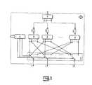
- FIG. 1represents a block diagram of the basic version of the phase control device according to the invention
- FIG. 2represents a principal diagram of the phased array antenna
- FIG. 3represents one group of radiating elements with outputs for the horizontal and the vertical component of the signal
- FIG. 4represents one version for realization of the phase control device according to the invention
- FIG. 5represents a block diagram of a phased array antenna with a set of phase control devices, like the one shown on FIG. 4
- the phase control device( FIG. 1 ) has several inputs 1 , to which the outputs of the groups G of antenna radiating elements 7 are connected (shown on FIGS. 2 and 3 ). Inputs 1 are connected to the block of switches 2 , whose outputs are connected to internal summators 3 . Group signal is obtained at the outputs of each of summators 3 as a result of the control of the state of switches in the block of switches 2 . In this way dynamic grouping of the signals is obtained.
- the output of each summator 3is connected to a corresponding input of common summation circuit 4 trough phase shifting elements 5 .
- Output of the circuit 4is the output of the phase control device.
- Outputs of the block for control of the phase 6are connected to the control inputs of the block of switches 2 .
- the phase control device on FIG. 1is denoted with the letter “ ⁇ ”.
- a principal diagram of a phased array antenna( FIG. 2 ) includes several phase control devices ⁇ 1 , ⁇ 2 . . . ⁇ n , like the one described above, to which inputs are connected the outputs of the groups G of radiating elements 7 .
- the outputs of the phase control devicesare connected to the inputs of summation circuit 8 of the phased array antenna.
- FIG. 3A way of grouping of antenna radiating elements 7 of the phased array is shown on FIG. 3 .
- the figureillustrates group G of twelve radiating elements 7 . This is a static grouping since it is not changed in the process of operation of the antenna.
- Each radiating element 7has an output V for the vertical component and an output H for the horizontal component of the electromagnetic field.
- Summation circuit 9sums outputs H, while summation circuit 10 —outputs V.
- Group signals for the horizontal and the vertical component of the electromagnetic field obtained at the outputs of summation circuits 9 and 10are amplified by amplifiers 11 and 12 . Obtained signals are phase controlled by the corresponding phase control device for the given group radiating elements 6 .
- the diagram of grouping of the radiating elements from FIG. 3is denoted as “G”.
- the phase control device shown on FIG. 4is similar to that shown on FIG. 1 .
- the phase control device shown on FIG. 4has eight high frequency inputs 1 RFI 1 . . . RFI 8 , two high frequency outputs RFO 1 and RFO 2 , a block of switches 2 and eight internal summators 3 with eight inputs each.
- the outputs of the first four summators 3are connected to the first summation circuit 4 trough the first set of phase shifting elements 5
- the outputs of the second four summators 3are connected to the second summation circuit 4 trough the second set of phase shifting elements 5 .
- the two sets of phase shifting elements 5may be with identical values, but that is not obligatory.
- the outputs of the controlling block 6are connected to the control inputs of the block of switches 2 .
- the block diagram of the phased arraydepicts the overall architecture of the phased array antenna, realized with phase control devices ⁇ according to the present invention.
- Output signal of the phased arrayis obtained at the output of summation circuit 14 , to which outputs are connected the outputs of each of the phase control devices ⁇ .
- phase control deviceThe operation of the phase control device according to the present invention is:
- Signals from the groups G of radiating elements 7are applied to the inputs of the phase control device ⁇ (FIG. 1 ).
- the state of each one of the switches from the block of switchesis set 2 .
- signals with approximately equal phasesare grouped.
- Group signals at the outputs of each one of the summators 3are phase shifted trough a corresponding phase shifting element 5 and in this way all the group signals are led to the same phase state so that the summation circuit 4 can sum them.
- the same operationsare performed for each one of the groups of radiating elements connected to the particular phase control device (FIG. 5 ).
- Output signals formed in this wayare in principal of equal phase states and are summed by the summation circuit 14 , which forms the output signal of the phased array antenna.
- Each one of the radiating elements 7has two outputs for the vertical and the horizontal component of the electromagnetic field. Signals from all outputs for the vertical component of the electromagnetic field are summed by the summation circuit 9 , thus forming a common signal for the group of twelve radiating elements 7 for the vertical component of the electromagnetic field. In the same way signals from all outputs for the horizontal component of the electromagnetic field are summed by the summation circuit 10 , thus forming a common signal for the group of twelve radiating elements representative for the horizontal component of the electromagnetic field.
- the two componentsare then amplified by the amplifiers 11 and 12 , which form the two outputs of the group G of radiating elements for the vertical V and the horizontal H component of the electromagnetic field accordingly.
- Phase controlis applied on these two signals and scanning of the main beam of the phased array is obtained by applying phase control on the two outputs of the group of radiating elements as a whole.
- Polarization control of the antennais obtained by proper selection of the phase relations between the horizontal and the vertical component of the electromagnetic field of the group of radiating elements. It is seen that scanning of the main beam of the antenna and its polarization control is obtained by applying phase control on the two outputs of the group G of radiating elements 7 .
- the horizontal and the vertical component of the electromagnetic fieldare considered, but the same principal could be applied to every two orthogonal components of the electromagnetic field.
- a necessary and sufficient condition for adequate operation of the antennais the selection of two orthogonal components of the electromagnetic field, which are formed at the output of the radiating elements 7 and at the output of the group of radiating elements G.
- the two orthogonal output components at the output of the radiating elements 7 and at the output of the group of radiating elements Gmust not necessarily coincide. It is possible to perform transformation of the polarizations inside the summation circuits 9 and 10 .
- the main goal of the group of radiating elements Gis to reduce the number of the signals on which phase control is applied and in this way to reduce further the number of the phase control devices needed for realization of the antenna.
- phase control device presented on FIG. 4operates in the following way:
- Input signals with random phases uniformly distributed in the range 0° to 360°are amplified by the amplifiers 13 and are fed at the inputs of the block of switches 2 .
- the input signalswhich are with close phases in the range 0° to 180° are guided to the first group of summators 3 and correspondingly to the first set of phase shifting elements 5
- the input signals with close phases in the range 180° to 360°are guided to the second group of summators 3 and correspondingly to the second set of phase shifting elements 5 .
- the input signalsare divided in two groups so that the phase difference between each two signals in each group is not bigger than 180°.
- the key combination of the switches in the block 2are selected in a way that signals with a phase difference not greater than 45° are summed by the summators 3 before phase shifting elements 5 .
- the output signals from phase shifting elements 5 from each one of the two groupsare with approximately equal phases and the phase difference between the two groups of signals is approximately 180°.
- the signals from each one of the two groupsare summed by the two summators 4 and the two summation signals at the output of the summators 4 form the two high frequency outputs RFO 1 and RFO 2 of the phase control device ⁇ .
- the phase difference of the two output signalsis approximately 180°.
- phase control deviceThe main role of the phase control device is to apply phase control on signals obtained from the radiating elements 7 .
- phase controlis applied on the group signal from the group of radiating elements 7 , but the same control can be applied on the signal from the single radiating element.
- Summation circuits for the high frequency bandcontain set of microwave power summators.
- the main goal of these circuitsis to sum the signals at the outputs of the phase control devices and to provide an additional 180° phase shift for selected signals.
- the circuit shown on FIG. 5operates in the following way:
- the input signalcontains information for two orthogonal components of the electromagnetic field. Separated signals for the two orthogonal components of the electromagnetic field are obtained at the output of the radiating elements 7 (in this particular case V and H).
- the components of the electromagnetic fieldwhich are of the same type, are grouped in groups of twelve radiating elements, summed by the internal summators 9 , 10 (see FIG. 3 ) and are then amplified by the amplifiers 11 , 12 of the group of radiating elements. In this way two signals are obtained, which contain information about the average value of the two orthogonal components from the corresponding twelve radiating elements.
- the signals at the output of the group of radiating elementsare with different phases, depending on the antenna polarization and on the position of the radiating elements 7 on the aperture of the antenna.
- a further goalis to apply an additional phase shift on the signals coming from the groups of radiating elements so that (differences) in their phases are compensated and signals with equal phases are obtained.
- Signals from the groups of radiating elements Gcome at the input of the phase control devices ⁇ .
- the phase control devicesblock of switches 2 and summators 3 signals at their inputs with phases in the range 0°-360° are divided in two groups of signals with phases in the ranges 0°-180° and 180°-360° respectively.
- Signalstaking part in a particular group, are phase equalized by means of internal for the phase control devices phase shifting elements 5 and are then summed.
- the summation signalis amplified and comes to one of the outputs of the phase control device depending on whether the phases of the signals before summation were in the range 0°-180° or 180°-360°.
- signals with phases approximately equal to 0°are obtained, while at the second output signals with phases approximately equal to 180° are obtained.
- Further additional phase shiftis applied in the power summators 8 for the signals from the second outputs of the phase control devices so that they are phase equalized with the signals from the first outputs and all the signals are then summed by the common summation circuit 14 .
- the phase control devicewhen used in the way described above, is capable of moving the antenna beam in the limited spatial angle, determined by the size of the group of radiating elements, as well as of controlling the polarization of the antenna with respect to the selected phase shifting elements 5 inside the phase control devices ⁇ .
Landscapes
- Variable-Direction Aerials And Aerial Arrays (AREA)
Abstract
Description
Claims (10)
Applications Claiming Priority (3)
| Application Number | Priority Date | Filing Date | Title |
|---|---|---|---|
| BG105597 | 2001-06-14 | ||
| BG105597ABG64659B1 (en) | 2001-06-14 | 2001-06-14 | Method for scanning an antenna array and phase-adjustment device for the materialization thereof |
| PCT/BG2002/000008WO2002103842A1 (en) | 2001-06-14 | 2002-06-13 | A method and device for scanning a phased array antenna |
Publications (2)
| Publication Number | Publication Date |
|---|---|
| US20040233103A1 US20040233103A1 (en) | 2004-11-25 |
| US6897806B2true US6897806B2 (en) | 2005-05-24 |
Family
ID=3928410
Family Applications (1)
| Application Number | Title | Priority Date | Filing Date |
|---|---|---|---|
| US10/480,622Expired - Fee RelatedUS6897806B2 (en) | 2001-06-14 | 2002-06-13 | Method and device for scanning a phased array antenna |
Country Status (4)
| Country | Link |
|---|---|
| US (1) | US6897806B2 (en) |
| EP (1) | EP1417732A1 (en) |
| BG (1) | BG64659B1 (en) |
| WO (1) | WO2002103842A1 (en) |
Cited By (8)
| Publication number | Priority date | Publication date | Assignee | Title |
|---|---|---|---|---|
| US20060197713A1 (en)* | 2003-02-18 | 2006-09-07 | Starling Advanced Communication Ltd. | Low profile antenna for satellite communication |
| US20070085744A1 (en)* | 2005-10-16 | 2007-04-19 | Starling Advanced Communications Ltd. | Dual polarization planar array antenna and cell elements therefor |
| US20070146222A1 (en)* | 2005-10-16 | 2007-06-28 | Starling Advanced Communications Ltd. | Low profile antenna |
| US20090231186A1 (en)* | 2008-02-06 | 2009-09-17 | Raysat Broadcasting Corp. | Compact electronically-steerable mobile satellite antenna system |
| US8964891B2 (en) | 2012-12-18 | 2015-02-24 | Panasonic Avionics Corporation | Antenna system calibration |
| US9026161B2 (en) | 2012-04-19 | 2015-05-05 | Raytheon Company | Phased array antenna having assignment based control and related techniques |
| US9583829B2 (en) | 2013-02-12 | 2017-02-28 | Panasonic Avionics Corporation | Optimization of low profile antenna(s) for equatorial operation |
| US12088013B2 (en) | 2021-03-30 | 2024-09-10 | Skyworks Solutions, Inc. | Frequency range two antenna array with switches for joining antennas for frequency range one communications |
Families Citing this family (11)
| Publication number | Priority date | Publication date | Assignee | Title |
|---|---|---|---|---|
| US10436928B2 (en)* | 2014-12-19 | 2019-10-08 | International Business Machines Corporation | Detection and imaging of subsurface high impedance contrast objects |
| GB2539734A (en) | 2015-06-25 | 2016-12-28 | Airspan Networks Inc | An antenna apparatus and method of performing spatial nulling within the antenna apparatus |
| GB2539730B (en) | 2015-06-25 | 2021-04-07 | Airspan Ip Holdco Llc | Node role assignment in networks |
| GB2539731B (en) | 2015-06-25 | 2021-08-04 | Airspan Ip Holdco Llc | Quality of service in wireless backhauls |
| EP3314963B1 (en) | 2015-06-25 | 2019-04-24 | Airspan Networks Inc. | Managing external interference in a wireless network |
| GB2539722B (en) | 2015-06-25 | 2021-10-13 | Airspan Ip Holdco Llc | Bearing calculation |
| GB2539735A (en) | 2015-06-25 | 2016-12-28 | Airspan Networks Inc | Sub-sampling antenna elements |
| GB2539733A (en) | 2015-06-25 | 2016-12-28 | Airspan Networks Inc | An antenna apparatus and method of configuring a transmission beam for the antenna apparatus |
| GB2539727B (en) | 2015-06-25 | 2021-05-12 | Airspan Ip Holdco Llc | A configurable antenna and method of operating such a configurable antenna |
| GB2539736A (en) | 2015-06-25 | 2016-12-28 | Airspan Networks Inc | Wireless network configuration using path loss determination between nodes |
| GB2539732A (en)* | 2015-06-25 | 2016-12-28 | Airspan Networks Inc | A configurable antenna and method of operating such a configurable antenna |
Citations (12)
| Publication number | Priority date | Publication date | Assignee | Title |
|---|---|---|---|---|
| US3816830A (en) | 1970-11-27 | 1974-06-11 | Hazeltine Corp | Cylindrical array antenna |
| US4041501A (en) | 1975-07-10 | 1977-08-09 | Hazeltine Corporation | Limited scan array antenna systems with sharp cutoff of element pattern |
| US4123759A (en)* | 1977-03-21 | 1978-10-31 | Microwave Associates, Inc. | Phased array antenna |
| US4612547A (en) | 1982-09-07 | 1986-09-16 | Nec Corporation | Electronically scanned antenna |
| US5079557A (en)* | 1990-12-24 | 1992-01-07 | Westinghouse Electric Corp. | Phased array antenna architecture and related method |
| US5854610A (en)* | 1997-11-13 | 1998-12-29 | Northrop Grumman Corporation | Radar electronic scan array employing ferrite phase shifters |
| US6016123A (en)* | 1994-02-16 | 2000-01-18 | Northern Telecom Limited | Base station antenna arrangement |
| US6184828B1 (en)* | 1992-11-18 | 2001-02-06 | Kabushiki Kaisha Toshiba | Beam scanning antennas with plurality of antenna elements for scanning beam direction |
| US20020080066A1 (en)* | 1998-04-06 | 2002-06-27 | Dent Paul W. | Multi-signal transmit array with low intermodulation |
| US20020167445A1 (en)* | 2001-03-28 | 2002-11-14 | Eden Richard C. | Method and device for precise geolocation of low-power, broadband, amplitude-modulated signals |
| US6504505B1 (en)* | 2000-10-30 | 2003-01-07 | Hughes Electronics Corporation | Phase control network for active phased array antennas |
| US6661375B2 (en)* | 2001-02-15 | 2003-12-09 | Roke Manor Research Limited | Beam steering in sub-arrayed antennae |
Family Cites Families (1)
| Publication number | Priority date | Publication date | Assignee | Title |
|---|---|---|---|---|
| WO1998005089A1 (en)* | 1996-07-25 | 1998-02-05 | Skygate International Technology Nv | A phase control device |
- 2001
- 2001-06-14BGBG105597Apatent/BG64659B1/enunknown
- 2002
- 2002-06-13USUS10/480,622patent/US6897806B2/ennot_activeExpired - Fee Related
- 2002-06-13EPEP02734924Apatent/EP1417732A1/ennot_activeWithdrawn
- 2002-06-13WOPCT/BG2002/000008patent/WO2002103842A1/ennot_activeApplication Discontinuation
Patent Citations (12)
| Publication number | Priority date | Publication date | Assignee | Title |
|---|---|---|---|---|
| US3816830A (en) | 1970-11-27 | 1974-06-11 | Hazeltine Corp | Cylindrical array antenna |
| US4041501A (en) | 1975-07-10 | 1977-08-09 | Hazeltine Corporation | Limited scan array antenna systems with sharp cutoff of element pattern |
| US4123759A (en)* | 1977-03-21 | 1978-10-31 | Microwave Associates, Inc. | Phased array antenna |
| US4612547A (en) | 1982-09-07 | 1986-09-16 | Nec Corporation | Electronically scanned antenna |
| US5079557A (en)* | 1990-12-24 | 1992-01-07 | Westinghouse Electric Corp. | Phased array antenna architecture and related method |
| US6184828B1 (en)* | 1992-11-18 | 2001-02-06 | Kabushiki Kaisha Toshiba | Beam scanning antennas with plurality of antenna elements for scanning beam direction |
| US6016123A (en)* | 1994-02-16 | 2000-01-18 | Northern Telecom Limited | Base station antenna arrangement |
| US5854610A (en)* | 1997-11-13 | 1998-12-29 | Northrop Grumman Corporation | Radar electronic scan array employing ferrite phase shifters |
| US20020080066A1 (en)* | 1998-04-06 | 2002-06-27 | Dent Paul W. | Multi-signal transmit array with low intermodulation |
| US6504505B1 (en)* | 2000-10-30 | 2003-01-07 | Hughes Electronics Corporation | Phase control network for active phased array antennas |
| US6661375B2 (en)* | 2001-02-15 | 2003-12-09 | Roke Manor Research Limited | Beam steering in sub-arrayed antennae |
| US20020167445A1 (en)* | 2001-03-28 | 2002-11-14 | Eden Richard C. | Method and device for precise geolocation of low-power, broadband, amplitude-modulated signals |
Non-Patent Citations (1)
| Title |
|---|
| P.S. Hall et al., Review of radio frequency beamforming techniques for scanned and multiple beam antennas, Microwaves, Antennas and Propagation, IEE Proceedings H, vol. 137(5), p. 293-303 , Oct. 1990.* |
Cited By (16)
| Publication number | Priority date | Publication date | Assignee | Title |
|---|---|---|---|---|
| US20090295656A1 (en)* | 2003-02-18 | 2009-12-03 | Starling Advanced Communications Ltd. | Low profile antenna for satellite communication |
| US7999750B2 (en) | 2003-02-18 | 2011-08-16 | Starling Advanced Communications Ltd. | Low profile antenna for satellite communication |
| US7768469B2 (en) | 2003-02-18 | 2010-08-03 | Starling Advanced Communications Ltd. | Low profile antenna for satellite communication |
| US7629935B2 (en) | 2003-02-18 | 2009-12-08 | Starling Advanced Communications Ltd. | Low profile antenna for satellite communication |
| US20060197713A1 (en)* | 2003-02-18 | 2006-09-07 | Starling Advanced Communication Ltd. | Low profile antenna for satellite communication |
| US7595762B2 (en) | 2005-10-16 | 2009-09-29 | Starling Advanced Communications Ltd. | Low profile antenna |
| US7663566B2 (en) | 2005-10-16 | 2010-02-16 | Starling Advanced Communications Ltd. | Dual polarization planar array antenna and cell elements therefor |
| US20070146222A1 (en)* | 2005-10-16 | 2007-06-28 | Starling Advanced Communications Ltd. | Low profile antenna |
| US20100201594A1 (en)* | 2005-10-16 | 2010-08-12 | Starling Advanced Communications Ltd. | Dual polarization planar array antenna and cell elements therefor |
| US7994998B2 (en) | 2005-10-16 | 2011-08-09 | Starling Advanced Communications Ltd. | Dual polarization planar array antenna and cell elements therefor |
| US20070085744A1 (en)* | 2005-10-16 | 2007-04-19 | Starling Advanced Communications Ltd. | Dual polarization planar array antenna and cell elements therefor |
| US20090231186A1 (en)* | 2008-02-06 | 2009-09-17 | Raysat Broadcasting Corp. | Compact electronically-steerable mobile satellite antenna system |
| US9026161B2 (en) | 2012-04-19 | 2015-05-05 | Raytheon Company | Phased array antenna having assignment based control and related techniques |
| US8964891B2 (en) | 2012-12-18 | 2015-02-24 | Panasonic Avionics Corporation | Antenna system calibration |
| US9583829B2 (en) | 2013-02-12 | 2017-02-28 | Panasonic Avionics Corporation | Optimization of low profile antenna(s) for equatorial operation |
| US12088013B2 (en) | 2021-03-30 | 2024-09-10 | Skyworks Solutions, Inc. | Frequency range two antenna array with switches for joining antennas for frequency range one communications |
Also Published As
| Publication number | Publication date |
|---|---|
| BG64659B1 (en) | 2005-10-31 |
| US20040233103A1 (en) | 2004-11-25 |
| BG105597A (en) | 2002-12-29 |
| WO2002103842A1 (en) | 2002-12-27 |
| EP1417732A1 (en) | 2004-05-12 |
Similar Documents
| Publication | Publication Date | Title |
|---|---|---|
| US6897806B2 (en) | Method and device for scanning a phased array antenna | |
| Hu et al. | An orthogonal hybrid analog–digital multibeam antenna array for millimeter-wave massive MIMO systems | |
| US4032922A (en) | Multibeam adaptive array | |
| US6366238B1 (en) | Phased array beamformer module driving two elements | |
| JP3502348B2 (en) | Adaptive array antenna, calibration amount calculation method and calibration method for adaptive array antenna receiving system | |
| US6208294B1 (en) | Array antenna receiving device | |
| US20070210959A1 (en) | Multi-beam tile array module for phased array systems | |
| US20120001801A1 (en) | Antenna System | |
| US20120108297A1 (en) | Antenna device for a radio base station in a cellular telephony system | |
| US6225947B1 (en) | Butler beam port combining for hexagonal cell coverage | |
| EP1281213B1 (en) | Phased array antenna data re-alignment | |
| EP1488478A2 (en) | Open loop array antenna beam steering architecture | |
| WO2015000519A1 (en) | A multi-beam antenna arrangement | |
| US6295026B1 (en) | Enhanced direct radiating array | |
| US6480154B1 (en) | Method and system for digital beam forming | |
| EP1266427B1 (en) | Digital phased array architecture and associated method | |
| WO2007040635A1 (en) | Improved thinned array antenna system | |
| US7548764B2 (en) | Method and system for generating multiple radiation patterns using transform matrix | |
| US7274328B2 (en) | Transmitting and receiving radio frequency signals using an active electronically scanned array | |
| Akbar et al. | Design of a scalable phased array antenna with a simplified architecture | |
| JP6875539B2 (en) | Beamforming antenna | |
| WO2015090427A1 (en) | Load balancing of dual-polarized antennas | |
| US6255990B1 (en) | Processor for two-dimensional array antenna | |
| CN116454621A (en) | Signal receiving method and device and planar phased array antenna | |
| US7492325B1 (en) | Modular electronic architecture |
Legal Events
| Date | Code | Title | Description |
|---|---|---|---|
| AS | Assignment | Owner name:SKYGATE INTERNATIONAL TECHNOLOGY N.V., BULGARIA Free format text:ASSIGNMENT OF ASSIGNORS INTEREST;ASSIGNOR:TOSHEV, ALEKSANDER GEORGLEV;REEL/FRAME:015363/0689 Effective date:20040219 | |
| AS | Assignment | Owner name:RAYSAT CYPRUS LIMITED, CYPRUS Free format text:DEED OF TRANSFER;ASSIGNOR:SKYTECH B.V.;REEL/FRAME:014738/0075 Effective date:20040325 Owner name:SKYGATE B.V., NETHERLANDS Free format text:ASSIGNMENT OF ASSIGNORS INTEREST;ASSIGNOR:SKYGATE INTERNATIONAL TECHNOLOGY N.V.;REEL/FRAME:014738/0001 Effective date:20040325 Owner name:SKYTECH B.V., NETHERLANDS Free format text:DEED OF TRANSFER;ASSIGNOR:SKYGATE B.V.;REEL/FRAME:014738/0040 Effective date:20040325 | |
| FPAY | Fee payment | Year of fee payment:4 | |
| AS | Assignment | Owner name:RAYSAT INC., VIRGINIA Free format text:ASSIGNMENT OF ASSIGNORS INTEREST;ASSIGNOR:RAYSAT CYPRUS LTD.;REEL/FRAME:028213/0880 Effective date:20120514 | |
| AS | Assignment | Owner name:GILAT SATELLITE NETWORKS, LTD., ISRAEL Free format text:ASSIGNMENT OF ASSIGNORS INTEREST;ASSIGNOR:RAYSAT, INC.;REEL/FRAME:029342/0666 Effective date:20120607 | |
| REMI | Maintenance fee reminder mailed | ||
| LAPS | Lapse for failure to pay maintenance fees | ||
| STCH | Information on status: patent discontinuation | Free format text:PATENT EXPIRED DUE TO NONPAYMENT OF MAINTENANCE FEES UNDER 37 CFR 1.362 | |
| FP | Lapsed due to failure to pay maintenance fee | Effective date:20130524 |