US6897483B2 - Second gallium nitride layers that extend into trenches in first gallium nitride layers - Google Patents
Second gallium nitride layers that extend into trenches in first gallium nitride layersDownload PDFInfo
- Publication number
- US6897483B2 US6897483B2US10/426,553US42655303AUS6897483B2US 6897483 B2US6897483 B2US 6897483B2US 42655303 AUS42655303 AUS 42655303AUS 6897483 B2US6897483 B2US 6897483B2
- Authority
- US
- United States
- Prior art keywords
- gallium nitride
- growth
- lateral
- nitride layer
- trenches
- Prior art date
- Legal status (The legal status is an assumption and is not a legal conclusion. Google has not performed a legal analysis and makes no representation as to the accuracy of the status listed.)
- Expired - Lifetime, expires
Links
- 229910002601GaNInorganic materials0.000titleclaimsabstractdescription174
- JMASRVWKEDWRBT-UHFFFAOYSA-NGallium nitrideChemical compound[Ga]#NJMASRVWKEDWRBT-UHFFFAOYSA-N0.000titleclaimsabstractdescription171
- 239000004065semiconductorSubstances0.000claimsabstractdescription51
- 230000007547defectEffects0.000claimsabstractdescription25
- 238000004377microelectronicMethods0.000claimsabstractdescription14
- 239000000758substrateSubstances0.000claimsdescription33
- 230000012010growthEffects0.000description79
- RGGPNXQUMRMPRA-UHFFFAOYSA-NtriethylgalliumChemical compoundCC[Ga](CC)CCRGGPNXQUMRMPRA-UHFFFAOYSA-N0.000description16
- 238000000034methodMethods0.000description14
- VYPSYNLAJGMNEJ-UHFFFAOYSA-NSilicium dioxideChemical compoundO=[Si]=OVYPSYNLAJGMNEJ-UHFFFAOYSA-N0.000description13
- QGZKDVFQNNGYKY-UHFFFAOYSA-NAmmoniaChemical compoundNQGZKDVFQNNGYKY-UHFFFAOYSA-N0.000description12
- 238000004519manufacturing processMethods0.000description10
- 229910010271silicon carbideInorganic materials0.000description9
- PMHQVHHXPFUNSP-UHFFFAOYSA-Mcopper(1+);methylsulfanylmethane;bromideChemical compoundBr[Cu].CSCPMHQVHHXPFUNSP-UHFFFAOYSA-M0.000description7
- 239000000377silicon dioxideSubstances0.000description7
- 238000000927vapour-phase epitaxyMethods0.000description7
- 229910000069nitrogen hydrideInorganic materials0.000description6
- 239000002243precursorSubstances0.000description6
- GYHNNYVSQQEPJS-UHFFFAOYSA-NGalliumChemical compound[Ga]GYHNNYVSQQEPJS-UHFFFAOYSA-N0.000description5
- 208000012868OvergrowthDiseases0.000description5
- 229910052681coesiteInorganic materials0.000description5
- 229910052906cristobaliteInorganic materials0.000description5
- 239000003085diluting agentSubstances0.000description5
- 229910052733galliumInorganic materials0.000description5
- 239000000463materialSubstances0.000description5
- 229910052682stishoviteInorganic materials0.000description5
- 229910052905tridymiteInorganic materials0.000description5
- 238000005530etchingMethods0.000description4
- 229910021529ammoniaInorganic materials0.000description3
- 238000001816coolingMethods0.000description3
- 238000009792diffusion processMethods0.000description3
- 229910052738indiumInorganic materials0.000description3
- APFVFJFRJDLVQX-UHFFFAOYSA-Nindium atomChemical compound[In]APFVFJFRJDLVQX-UHFFFAOYSA-N0.000description3
- 125000002524organometallic groupChemical group0.000description3
- 238000011160researchMethods0.000description3
- 229910052594sapphireInorganic materials0.000description3
- 239000010980sapphireSubstances0.000description3
- HBMJWWWQQXIZIP-UHFFFAOYSA-Nsilicon carbideChemical compound[Si+]#[C-]HBMJWWWQQXIZIP-UHFFFAOYSA-N0.000description3
- IJGRMHOSHXDMSA-UHFFFAOYSA-NAtomic nitrogenChemical compoundN#NIJGRMHOSHXDMSA-UHFFFAOYSA-N0.000description2
- 229910045601alloyInorganic materials0.000description2
- 239000000956alloySubstances0.000description2
- 229910052782aluminiumInorganic materials0.000description2
- XAGFODPZIPBFFR-UHFFFAOYSA-NaluminiumChemical compound[Al]XAGFODPZIPBFFR-UHFFFAOYSA-N0.000description2
- 230000008859changeEffects0.000description2
- 238000011161developmentMethods0.000description2
- 239000007789gasSubstances0.000description2
- 230000007246mechanismEffects0.000description2
- 230000000877morphologic effectEffects0.000description2
- 125000004433nitrogen atomChemical groupN*0.000description2
- 235000012239silicon dioxideNutrition0.000description2
- JBRZTFJDHDCESZ-UHFFFAOYSA-NAsGaChemical compound[As]#[Ga]JBRZTFJDHDCESZ-UHFFFAOYSA-N0.000description1
- 229910000807Ga alloyInorganic materials0.000description1
- 229910001218Gallium arsenideInorganic materials0.000description1
- 229910007991Si-NInorganic materials0.000description1
- XUIMIQQOPSSXEZ-UHFFFAOYSA-NSiliconChemical compound[Si]XUIMIQQOPSSXEZ-UHFFFAOYSA-N0.000description1
- 229910006294Si—NInorganic materials0.000description1
- RNQKDQAVIXDKAG-UHFFFAOYSA-Naluminum galliumChemical compound[Al].[Ga]RNQKDQAVIXDKAG-UHFFFAOYSA-N0.000description1
- AJGDITRVXRPLBY-UHFFFAOYSA-Naluminum indiumChemical compound[Al].[In]AJGDITRVXRPLBY-UHFFFAOYSA-N0.000description1
- 229910021486amorphous silicon dioxideInorganic materials0.000description1
- 238000003491arrayMethods0.000description1
- 125000004429atomChemical group0.000description1
- QVGXLLKOCUKJST-UHFFFAOYSA-Natomic oxygenChemical compound[O]QVGXLLKOCUKJST-UHFFFAOYSA-N0.000description1
- 230000008901benefitEffects0.000description1
- 230000015572biosynthetic processEffects0.000description1
- 238000004581coalescenceMethods0.000description1
- 230000002860competitive effectEffects0.000description1
- 230000000295complement effectEffects0.000description1
- 238000007796conventional methodMethods0.000description1
- 238000005336crackingMethods0.000description1
- 239000013078crystalSubstances0.000description1
- 238000000151depositionMethods0.000description1
- 230000008021depositionEffects0.000description1
- 238000000407epitaxyMethods0.000description1
- 239000010408filmSubstances0.000description1
- 230000004907fluxEffects0.000description1
- IXCSERBJSXMMFS-UHFFFAOYSA-Nhcl hclChemical compoundCl.ClIXCSERBJSXMMFS-UHFFFAOYSA-N0.000description1
- 239000001257hydrogenSubstances0.000description1
- 229910052739hydrogenInorganic materials0.000description1
- 125000004435hydrogen atomChemical class[H]*0.000description1
- 238000004518low pressure chemical vapour depositionMethods0.000description1
- 230000000873masking effectEffects0.000description1
- 229910052757nitrogenInorganic materials0.000description1
- 230000005693optoelectronicsEffects0.000description1
- 229910052760oxygenInorganic materials0.000description1
- 239000001301oxygenSubstances0.000description1
- 239000012071phaseSubstances0.000description1
- 238000000206photolithographyMethods0.000description1
- 238000012545processingMethods0.000description1
- 230000001902propagating effectEffects0.000description1
- 239000000376reactantSubstances0.000description1
- 230000009467reductionEffects0.000description1
- 229910052710siliconInorganic materials0.000description1
- 239000010703siliconSubstances0.000description1
- 230000035882stressEffects0.000description1
- 239000000126substanceSubstances0.000description1
- 230000008646thermal stressEffects0.000description1
- 239000010409thin filmSubstances0.000description1
- 229910052984zinc sulfideInorganic materials0.000description1
Images


Classifications
- H—ELECTRICITY
- H01—ELECTRIC ELEMENTS
- H01L—SEMICONDUCTOR DEVICES NOT COVERED BY CLASS H10
- H01L21/00—Processes or apparatus adapted for the manufacture or treatment of semiconductor or solid state devices or of parts thereof
- H01L21/02—Manufacture or treatment of semiconductor devices or of parts thereof
- H01L21/04—Manufacture or treatment of semiconductor devices or of parts thereof the devices having potential barriers, e.g. a PN junction, depletion layer or carrier concentration layer
- H01L21/18—Manufacture or treatment of semiconductor devices or of parts thereof the devices having potential barriers, e.g. a PN junction, depletion layer or carrier concentration layer the devices having semiconductor bodies comprising elements of Group IV of the Periodic Table or AIIIBV compounds with or without impurities, e.g. doping materials
- H—ELECTRICITY
- H01—ELECTRIC ELEMENTS
- H01L—SEMICONDUCTOR DEVICES NOT COVERED BY CLASS H10
- H01L21/00—Processes or apparatus adapted for the manufacture or treatment of semiconductor or solid state devices or of parts thereof
- H01L21/02—Manufacture or treatment of semiconductor devices or of parts thereof
- H01L21/02104—Forming layers
- H01L21/02365—Forming inorganic semiconducting materials on a substrate
- H01L21/02612—Formation types
- H01L21/02617—Deposition types
- H01L21/02636—Selective deposition, e.g. simultaneous growth of mono- and non-monocrystalline semiconductor materials
- H01L21/02647—Lateral overgrowth
- H01L21/0265—Pendeoepitaxy
- H—ELECTRICITY
- H01—ELECTRIC ELEMENTS
- H01L—SEMICONDUCTOR DEVICES NOT COVERED BY CLASS H10
- H01L21/00—Processes or apparatus adapted for the manufacture or treatment of semiconductor or solid state devices or of parts thereof
- H01L21/02—Manufacture or treatment of semiconductor devices or of parts thereof
- H01L21/02104—Forming layers
- H01L21/02365—Forming inorganic semiconducting materials on a substrate
- H01L21/02367—Substrates
- H01L21/0237—Materials
- H01L21/02373—Group 14 semiconducting materials
- H01L21/02378—Silicon carbide
- H—ELECTRICITY
- H01—ELECTRIC ELEMENTS
- H01L—SEMICONDUCTOR DEVICES NOT COVERED BY CLASS H10
- H01L21/00—Processes or apparatus adapted for the manufacture or treatment of semiconductor or solid state devices or of parts thereof
- H01L21/02—Manufacture or treatment of semiconductor devices or of parts thereof
- H01L21/02104—Forming layers
- H01L21/02365—Forming inorganic semiconducting materials on a substrate
- H01L21/02436—Intermediate layers between substrates and deposited layers
- H01L21/02439—Materials
- H01L21/02455—Group 13/15 materials
- H01L21/02458—Nitrides
- H—ELECTRICITY
- H01—ELECTRIC ELEMENTS
- H01L—SEMICONDUCTOR DEVICES NOT COVERED BY CLASS H10
- H01L21/00—Processes or apparatus adapted for the manufacture or treatment of semiconductor or solid state devices or of parts thereof
- H01L21/02—Manufacture or treatment of semiconductor devices or of parts thereof
- H01L21/02104—Forming layers
- H01L21/02365—Forming inorganic semiconducting materials on a substrate
- H01L21/02518—Deposited layers
- H01L21/02521—Materials
- H01L21/02538—Group 13/15 materials
- H01L21/0254—Nitrides
- H—ELECTRICITY
- H01—ELECTRIC ELEMENTS
- H01L—SEMICONDUCTOR DEVICES NOT COVERED BY CLASS H10
- H01L21/00—Processes or apparatus adapted for the manufacture or treatment of semiconductor or solid state devices or of parts thereof
- H01L21/02—Manufacture or treatment of semiconductor devices or of parts thereof
- H01L21/02104—Forming layers
- H01L21/02365—Forming inorganic semiconducting materials on a substrate
- H01L21/02612—Formation types
- H01L21/02617—Deposition types
- H01L21/0262—Reduction or decomposition of gaseous compounds, e.g. CVD
- H—ELECTRICITY
- H01—ELECTRIC ELEMENTS
- H01L—SEMICONDUCTOR DEVICES NOT COVERED BY CLASS H10
- H01L21/00—Processes or apparatus adapted for the manufacture or treatment of semiconductor or solid state devices or of parts thereof
- H01L21/02—Manufacture or treatment of semiconductor devices or of parts thereof
- H01L21/02104—Forming layers
- H01L21/02365—Forming inorganic semiconducting materials on a substrate
- H01L21/02612—Formation types
- H01L21/02617—Deposition types
- H01L21/02636—Selective deposition, e.g. simultaneous growth of mono- and non-monocrystalline semiconductor materials
- H01L21/02639—Preparation of substrate for selective deposition
- H—ELECTRICITY
- H01—ELECTRIC ELEMENTS
- H01L—SEMICONDUCTOR DEVICES NOT COVERED BY CLASS H10
- H01L21/00—Processes or apparatus adapted for the manufacture or treatment of semiconductor or solid state devices or of parts thereof
- H01L21/02—Manufacture or treatment of semiconductor devices or of parts thereof
- H01L21/02104—Forming layers
- H01L21/02365—Forming inorganic semiconducting materials on a substrate
- H01L21/02612—Formation types
- H01L21/02617—Deposition types
- H01L21/02636—Selective deposition, e.g. simultaneous growth of mono- and non-monocrystalline semiconductor materials
- H01L21/02647—Lateral overgrowth
- H—ELECTRICITY
- H01—ELECTRIC ELEMENTS
- H01S—DEVICES USING THE PROCESS OF LIGHT AMPLIFICATION BY STIMULATED EMISSION OF RADIATION [LASER] TO AMPLIFY OR GENERATE LIGHT; DEVICES USING STIMULATED EMISSION OF ELECTROMAGNETIC RADIATION IN WAVE RANGES OTHER THAN OPTICAL
- H01S2304/00—Special growth methods for semiconductor lasers
- H01S2304/12—Pendeo epitaxial lateral overgrowth [ELOG], e.g. for growing GaN based blue laser diodes
- H—ELECTRICITY
- H01—ELECTRIC ELEMENTS
- H01S—DEVICES USING THE PROCESS OF LIGHT AMPLIFICATION BY STIMULATED EMISSION OF RADIATION [LASER] TO AMPLIFY OR GENERATE LIGHT; DEVICES USING STIMULATED EMISSION OF ELECTROMAGNETIC RADIATION IN WAVE RANGES OTHER THAN OPTICAL
- H01S5/00—Semiconductor lasers
- H01S5/02—Structural details or components not essential to laser action
- H01S5/0206—Substrates, e.g. growth, shape, material, removal or bonding
- H01S5/021—Silicon based substrates
Definitions
- This inventionrelates to microelectronic devices and fabrication methods, and more particularly to gallium nitride semiconductor devices and fabrication methods therefor.
- gallium nitrideis being widely investigated for microelectronic devices including but not limited to transistors, field emitters and optoelectronic devices. It will be understood that, as used herein, gallium nitride also includes alloys of gallium nitride such as aluminum gallium nitride, indium gallium nitride and aluminum indium gallium nitride.
- a major problem in fabricating gallium nitride-based microelectronic devicesis the fabrication of gallium nitride semiconductor layers having low defect densities. It is known that one contributor to defect density is the substrate on which the gallium nitride layer is grown. Accordingly, although gallium nitride layers have been grown on sapphire substrates, it is known to reduce defect density by growing gallium nitride layers on aluminum nitride buffer layers which are themselves formed on silicon carbide substrates. Notwithstanding these advances, continued reduction in, defect density is desirable.
- gallium nitride structuresthrough openings in a mask.
- undesired ridge growth or lateral overgrowthmay occur under certain conditions.
- a gallium nitride layerinto a trench in the gallium nitride layer, to thereby form a lateral gallium nitride semiconductor layer.
- One or more microelectronic devicesmay then be formed in the lateral gallium nitride semiconductor layer. It has been found, according to the present invention, that dislocation defects do not significantly propagate laterally into the lateral gallium nitride semiconductor layer, so that the lateral gallium nitride semiconductor; layer is relatively defect free.
- the lateral gallium nitride semiconductor layermay be laterally grown using metalorganic vapor phase epitaxy (MOVPE).
- MOVPEmetalorganic vapor phase epitaxy
- the lateral gallium nitride layermay be laterally grown using triethylgallium (TEG) and ammonia (NH 3 ) precursors at 1000-1100° C. and 45 Torr.
- TEGtriethylgallium
- NH 3ammonia
- TEG at 13-39 ⁇ mol/min and NH 3 at 1500 sccmare used in combination with 3000 sccm H 2 diluent.
- TEG at 26 ⁇ mol/min, NH 3 at 1500 sccm and H 2 at 3000 sccm at a temperature of 1100° C. and 45 Torrare used.
- the gallium nitride layerpreferably is formed on a substrate such as 6H—SiC(0001), which itself includes a buffer layer such as aluminum nitride thereon.
- a substratesuch as 6H—SiC(0001)
- Other substratessuch as sapphire, and other buffer layers such as low temperature gallium nitride, may be used. Multiple substrate layers and buffer layers also may be used.
- the gallium nitride layer including the trenchmaybe formed by forming a trench in a gallium nitride layer.
- the trenchmay be formed by forming a post on the gallium nitride layer, the post defining the trench.
- a series of alternating trenches and postsis preferably formed. Trenches and/or posts may be formed by selective etching, selective epitaxial growth, combinations of etching and growth, or other techniques.
- the trenchesmay extend into the buffer layer and into the substrate.
- the gallium nitride layeris laterally grown into the trench, to thereby form the lateral gallium nitride semiconductor layer of lower defect density than the defect density of the gallium nitride layer. Some vertical growth may also occur.
- the laterally grown gallium nitride semiconductor layeris vertically grown while propagating the lower defect density. Vertical growth may also take place simultaneous with the lateral growth.
- Gallium nitride semiconductor structurescomprise a gallium nitride layer including a trench, and a lateral gallium nitride layer that extends into the trench.
- a vertical gallium nitride layerextends from the lateral gallium nitride layer.
- At least one microelectronic deviceis included in the vertical gallium nitride layer.
- a series of alternating trenches and postsmay be provided.
- the gallium nitride layerincludes a predetermined defect density, and the lateral gallium nitride layer is of lower defect density than the predetermined defect density.
- FIGS. 1-5are cross-sectional views of first embodiments of gallium nitride semiconductor structures during intermediate fabrication steps according to the present invention.
- FIGS. 6-10are cross-sectional views of second embodiments of gallium nitride semiconductor structures during intermediate fabrication steps according to the present invention.
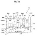
- FIGS. 11-15are cross-sectional views of third embodiments of gallium nitride semiconductor structures during intermediate fabrication steps according to the present invention.
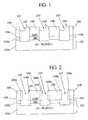
- an underlying gallium nitride layer 104is grown on a substrate 102 .
- the substrate 102may include a 6H—SiC(0001) substrate 102 a and an aluminum nitride buffer layer 102 b .
- the crystallographic designation conventions used hereinare well known to those having skill in the art, and need not be described further.
- the gallium nitride layer 104may be between 1.0 and 2.0 ⁇ m thick, and may be grown at 1000° C.
- the underlying gallium nitride layer 104includes a plurality of sidewalls 105 therein.
- the sidewalls 105may be thought of as being defined by a plurality of spaced apart posts 106 , that also may be referred to as “mesas”, “pedestals” or “columns”.
- the sidewalls 105may also be thought of as: being defined by a plurality of trenches 107 , also referred to as “wells” in the underlying gallium nitride layer 104 .
- the sidewalls 105may also be thought of as being defined by a series of alternating trenches 107 and posts 106 .
- the posts 106 and the trenches 107 that define the sidewalls 105may be fabricated by selective etching and/or selective epitaxial growth and/or other conventional techniques. Moreover, it will also be understood that the sidewalls need not be orthogonal to the substrate 102 , but rather may be oblique thereto. Finally, it will also be understood that although the sidewalls 105 are shown in cross-section in FIG. 1 , the posts 106 and trenches 107 may define elongated regions that are straight, V-shaped or have other shapes. As shown in FIG.
- the trenches 107may extend into the buffer layer 102 b and into the substrate 102 a , so that subsequent gallium nitride growth occurs preferentially on the sidewalls 105 rather than on the trench floors.
- the trenchesmay not extend into the substrate 102 a , and also may not extend into buffer layer 102 b , depending, for example, on the trench geometry and the lateral versus vertical growth rates of the gallium nitride.
- the sidewalls 105 of the underlying gallium nitride layer 104are laterally grown to form a lateral gallium nitride layer 108 a in the trenches 107 .
- Lateral growth of gallium nitridemay be obtained at 1000-1100° C. and 45 Torr.
- the precursors TEG at 13-39 ⁇ mol/min and NH 3 at 1500 sccmmay be used in combination with a 3000 sccm H 2 diluent. If gallium nitride alloys are formed, additional conventional precursors of aluminum or indium, for example, may also be used.
- lateralmeans a direction that is orthogonal to the sidewalls 105 . It will also be understood that some vertical growth on the posts 106 may also take place during the lateral growth from sidewalls 105 . As used herein, the term “vertical” denotes a directional parallel to the sidewalls 105 .
- continued growth of the lateral gallium nitride layer 108 acauses vertical growth onto the underlying gallium nitride layer 104 , specifically onto the posts 106 , to form a vertical gallium nitride layer 108 b .
- Growth conditions for vertical growthmay be maintained as was described in connection with FIG. 2 .
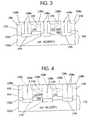
- continued vertical growth into trenches 107may take place at the bottom of the trenches.
- growthis allowed to continue until the lateral growth fronts coalesce in the trenches 107 at the interfaces 108 c , to form a continuous gallium nitride semiconductor layer in the trenches.
- the total growth timemay be approximately 60 minutes.
- microelectronic devices 110may then be formed in the lateral gallium nitride semiconductor layer 108 a .
- Devicesmay also be formed in vertical gallium nitride layer 108 b.
- gallium nitride semiconductor structures 100include the substrate 102 .
- the substratemay be sapphire or gallium nitride or other conventional substrates.
- the substrateincludes the 6H—SiC(0001) substrate 102 a and the aluminum nitride buffer layer 102 b on the silicon carbide substrate 102 a .
- the aluminum nitride buffer layer 102 bmay be 0.1 ⁇ m thick.
- the fabrication of the substrate 102is well known to those having skill in the art and need not be described further. Fabrication of silicon carbide substrates are described, for example, in U.S. Pat. No. 4,865,685 to Palmour; U.S. Pat. No. Re 34,861 to Davis et al.; U.S. Pat. No. 4,912,064 to Kong et al. and U.S. Pat. No. 4,946,547 to Palmour et al., the disclosures of which are hereby incorporated herein by reference.
- the underlying gallium nitride layer 104is also included on the buffer layer 102 b opposite the substrate 102 a .
- the underlying gallium nitride layer 104may be between about 1.0 and 2.0 ⁇ m thick, and may be formed using metalorganic vapor phase epitaxy (MOVPE).
- MOVPEmetalorganic vapor phase epitaxy
- the underlying gallium nitride layergenerally has an undesired relatively high defect density. For example, dislocation densities of between about 10 8 and 10 10 cm ⁇ 2 may be present in the underlying gallium nitride layer. These high defect densities may result from mismatches in lattice parameters between the buffer layer 102 b and the underlying gallium nitride layer 104 , and/or other causes. These high defect densities may impact the performance of microelectronic devices formed in the underlying gallium nitride layer 104 .
- the underlying gallium nitride layer 104includes the plurality of sidewalls 105 that maybe defined by the plurality of pedestals 106 and/or the plurality of trenches 107 .
- the sidewallsmay be oblique and of various elongated shapes.
- the lateral gallium nitride layer 108 aextends from the plurality of sidewalls 105 of the underlying gallium nitride layer 104 .
- the lateral gallium nitride layer 108 amay be formed using metalorganic vapor phase epitaxy at about 1000-1100° C. and 45 Torr. Precursors of triethygallium (TEG) at 13-39 ⁇ mol/min and ammonia (NH 3 ) at 1500 sccm may be used in combination with a 3000 sccm H 2 diluent, to form the lateral gallium nitride layer 108 a.
- TAGtriethygallium
- NH 3ammonia
- the gallium nitride semiconductor structure 100also includes the vertical gallium nitride layer 108 b that extends vertically from the posts 106 .
- the lateral gallium nitride layer 108 acoalesces at the interfaces 108 c to form a continuous lateral gallium nitride semiconductor layer 108 a in the trenches. It has been found that the dislocation densities in the underlying gallium nitride layer 104 generally do not propagate laterally from the sidewalls 105 with the same density as vertically from the underlying gallium nitride layer 104 . Thus, the lateral gallium nitride layer 108 a can have a relatively low defect density, for example less that 10 4 cm ⁇ 2 .
- the lateral gallium nitride layer 108 bmay form device quality gallium nitride semiconductor material.
- microelectronic devices 110may be formed in the lateral gallium nitride semiconductor layer 108 a . It will also be understood that a mask need not be used to fabricate the gallium nitride semiconductor structures 100 of FIG. 5 , because lateral growth is directed from the sidewalls 105 .
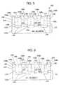
- gallium nitride semiconductor structures of FIG. 4are fabricated as was already described with regard to FIGS. 1-4 .
- the posts 106are masked with a mask 206 that includes an array of openings therein.
- the maskmay comprise silicon dioxide at thickness of 1000 ⁇ and may be deposited using low pressure chemical vapor deposition at 410° C. Other masking materials may be used.
- the maskmay be patterned using standard photolithography techniques and etched in a buffered HF solution.
- the openingsare 3 ⁇ m-wide openings that extend in parallel at distances of between 3 and 40 ⁇ m and that are oriented along the ⁇ 1 ⁇ overscore (1) ⁇ 00> direction on the lateral gallium nitride layer 108 a .
- the structurePrior to further processing, the structure may be dipped in a 50% hydrochloric acid (HCl) solution to remove surface oxides.
- HClhydrochloric acid
- the lateral gallium nitride semiconductor layer 108 ais grown through the array of openings to form a vertical gallium nitride layer 208 a in the openings. Growth of gallium nitride may be obtained, as was described in connection with FIG. 2 .
- the mask 206may be patterned to include an array of openings that extend along two orthogonal directions such as ⁇ 1 ⁇ overscore (1) ⁇ 00> and ⁇ 11 ⁇ overscore (2) ⁇ 0>.
- the openingscan form a rectangle of orthogonal striped patterns.
- the ratio of the edges of the rectangleis preferably proportional to the ratio of the growth rates of the ⁇ 11 ⁇ overscore (2) ⁇ 0 ⁇ and ⁇ 1 ⁇ overscore (1) ⁇ 01 ⁇ facets, for example, in a ratio of 1.4:1.
- the openingscan be equitriangular with respect to directions such as ⁇ 1 ⁇ overscore (1) ⁇ 00> and ⁇ 11 ⁇ overscore (2) ⁇ 0>.
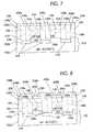
- lateral overgrowthis allowed to continue until the lateral growth fronts coalesce at the second interfaces 208 c on the mask 206 to form a continuous overgrown gallium nitride semiconductor layer 208 .
- the total growth timemay be approximately sixty minutes.
- microelectronic devices 210may then be formed in the second lateral gallium nitride layer 208 b .
- the microelectronic devicesmay also be formed in the vertical gallium nitride layer 208 a.
- defects that were present in continuous gallium nitride semiconductor layer 108may be reduced even further, to obtain device quality gallium nitride in the gallium nitride semiconductor structure 200 .
- gallium nitride semiconductor structures of FIG. 4are fabricated as was already described in connection with FIGS. 1-4 .
- a plurality of second sidewalls 305are formed.
- the second sidewalls 305may be formed by selective epitaxial growth of second posts 306 by etching second trenches 307 in the first posts 106 and/or combinations thereof.
- the second sidewalls 305need not be orthogonal to substrate 102 , but rather may be oblique.
- the second trenches 307need not be directly over the first posts 106 , but may be laterally offset therefrom.
- the second trenchesare preferably deep so that lateral growth preferentially occurs on the sidewalls 305 rather than on the bottom of second trenches 306 .
- the second sidewalls 305 of the second posts 306 and/or the second trenches 307are laterally grown to form a second lateral gallium nitride layer 308 a in the second trenches 307 .
- lateral growth of gallium nitridemay be obtained at 1000-1100° C. and 45 Torr.
- the precursors TEG at 13-39 ⁇ mol/min and NH 3 at 1500 sccmmay be used in combination with a 3000 sccm H 2 diluent. If gallium nitride alloys are formed, additional conventional precursors of aluminum or indium, for example, may also be used. It will also be understood that some vertical growth may take place on the second posts 306 during the lateral growth from the second sidewalls 305 .
- continued growth of the second lateral gallium nitride layer 308 acauses vertical growth onto the second posts 306 , to form a second vertical gallium nitride layer 308 b .
- vertical growth from the floors of the second trenches and from the tops of the second postsmay also take place. Growth conditions for vertical growth may be maintained as was described in connection with FIG. 12 .
- growthis allowed to continue until the lateral growth fronts coalesce in the second trenches 307 at the second interfaces 308 c to form a second continuous gallium nitride semiconductor layer 308 .
- the total growth timemay be approximately sixty minutes.
- microelectronic devices 310may then be formed in the second continuous gallium nitride semiconductor layer 308 .
- third embodiments of gallium nitride semiconductor structures 300 according to the present inventionmay be formed without the need to mask gallium nitride for purposes of defining lateral growth. Rather, lateral growth from first and second sidewalls may be used. By performing two separate lateral growths, the defect density may be reduced considerably.
- the first and second trenches 107 and 307 and the openings in the mask 206are preferably rectangular trenches and openings that preferably extend along the ⁇ 11 ⁇ overscore (2) ⁇ 0> and/or ⁇ 1 ⁇ overscore (1) ⁇ 00> directions on the underlying gallium nitride layer 104 or the first lateral gallium nitride layer 108 a .
- Truncated triangular stripes having (1 ⁇ overscore (1) ⁇ 01) slant facets and a narrow (0001) top facetmay be obtained for trenches and/or mask openings along the ⁇ 11 ⁇ overscore (2) ⁇ 0> direction.
- Rectangular stripes having a (0001) top facet, (11 ⁇ overscore (2) ⁇ 0) vertical side faces and (1 ⁇ overscore (1) ⁇ 01) slant facetsmay be grown along the ⁇ 1 ⁇ overscore (1) ⁇ 00> direction. For growth times up to 3 minutes, similar morphologies may be obtained regardless of orientation. The stripes develop into different shapes if the growth is continued.
- the amount of lateral growthgenerally exhibits a strong dependence on trench and/or mask opening orientation.
- the lateral growth rate of the ⁇ 1 ⁇ overscore (1) ⁇ 00> oriented trenches and/or mask openingsis generally much faster than those along ⁇ 11 ⁇ overscore (2) ⁇ 0>. Accordingly, it is most preferred to orient the trenches and/or mask openings, so that they extend along the ⁇ 1 ⁇ overscore (1) ⁇ 00> direction of the underlying gallium nitride layer 104 or the first lateral gallium nitride layer 108 a.
- Trenches and/or mask openings oriented along ⁇ 11 ⁇ overscore (2) ⁇ 0>may have wide (1 ⁇ overscore (1) ⁇ 00) slant facets and either a very narrow or no (0001) top facet depending on the growth conditions. This may be because (1 ⁇ overscore (1) ⁇ 01) is the most stable plane in the gallium nitride wurtzite crystal structure, and the growth rate of this plane is lower than that of others.
- the ⁇ 1 ⁇ overscore (1) ⁇ 01 ⁇ planes of the ⁇ 1 ⁇ overscore (1) ⁇ 00> oriented trenches and/or mask openingsmay be wavy, which implies the existence of more than one Miller index. It appears that competitive growth of selected ⁇ 1 ⁇ overscore (1) ⁇ 01 ⁇ planes occurs during the deposition which causes these planes to become unstable and which causes their growth rate to increase relative to that of the (1 ⁇ overscore (1) ⁇ 01) of trenches and/or mask openings oriented along ⁇ 11 ⁇ overscore (2) ⁇ 0>.
- the morphologies of the gallium nitride layers selectively grown from trenches and/or mask openings oriented along ⁇ 1 ⁇ overscore (1) ⁇ 00>are also generally a strong function of the growth temperatures.
- Layers grown at 1000° C.may possess a truncated triangular shape. This morphology may gradually change to a rectangular cross-section as the growth temperature is increased. This shape change may occur as a result of the increase in the diffusion coefficient and therefore the flux of the gallium species along the (0001) top plane onto the ⁇ 1 ⁇ overscore (1) ⁇ 01 ⁇ planes with an increase in growth temperature. This may result in a decrease in the growth rate of the (0001) plane and an increase in that of the ⁇ 1 ⁇ overscore (1) ⁇ 01 ⁇ . This phenomenon has also been observed in the selective growth of gallium arsenide on silicon dioxide. Accordingly, temperatures of 1100° C. appear to be most preferred.
- the morphological development of the gallium nitride regionsalso appears to depend on the flow rate of the TEG.
- An increase in the supply of TEGgenerally increases the growth rate in both the lateral and the vertical directions.
- the lateral/vertical growth rate ratiodecrease from 1.7 at the TEG flow rate of 13 ⁇ mol/min to 0.86 at 39 ⁇ mol.min.
- This increased influence on growth rate along ⁇ 0001> relative to that of ⁇ 11 ⁇ overscore (2) ⁇ 0> with TEG flow ratemay be related to the type of reactor employed, wherein the reactant gases flow vertically and perpendicular to the substrate.
- the considerable increase in the concentration of the gallium species on the surfacemay sufficiently impede their diffusion to the ⁇ 1 ⁇ overscore (1) ⁇ 01 ⁇ planes such that chemisorption and gallium nitride growth occur more readily on the (0001) plane.
- Continuous 2 ⁇ m thick gallium nitride semiconductor layersmay be obtained using 3 ⁇ m wide trenches and/or mask openings spaced 7 ⁇ m apart and oriented along ⁇ 1 ⁇ overscore (1) ⁇ 00>, at 1100° C. and a TEG flow rate of 26 ⁇ mol/min.
- the continuous gallium nitride semiconductor layersmay include subsurface voids that form when two growth fronts coalesce. These voids may occur most often using lateral growth conditions wherein rectangular trenches and/or mask openings having vertical ⁇ 11 ⁇ overscore (2) ⁇ 0 ⁇ side facets developed.
- the continuous gallium nitride semiconductor layersmay have a microscopically flat and pit-free surface.
- the surfaces of the laterally grown gallium nitride layersmay include a terrace structure having an average step height of 0.32 nm. This terrace structure may be related to the laterally grown gallium nitride, because it is generally not included in much larger area films grown only on aluminum nitride buffer layers.
- the average RMS roughness valuesmay be similar to the values obtained for the underlying gallium nitride layer 104 .
- Threading dislocationsoriginating from the interface between the underlying gallium nitride layer 104 and the buffer layer 102 b , appear to propagate to the top surface of the underlying gallium nitride layer 104 .
- the dislocation density within these regionsis approximately 10 9 cm ⁇ 2 .
- threading dislocationsdo not appear to readily propagate laterally. Rather, the lateral gallium nitride regions 108 a and 308 a contain only a few dislocations. These few dislocations may be formed parallel to the (0001) plane via the extension of the vertical threading dislocations after a 90° bend in the regrown region. These dislocations do not appear to propagate to the top surface of the overgrown gallium nitride layer.
- the formation mechanism of the selectively grown gallium nitride layersis lateral epitaxy.
- the two main stages of this mechanismare vertical growth and lateral growth.
- Ga or N atomsshould not readily bond to the mask surface in numbers and for a time sufficient to cause gallium nitride nuclei to form. They would either evaporate or diffuse along the mask surface to the opening in the mask or to the vertical gallium nitride surfaces which have emerged. During lateral growth, the gallium nitride grows simultaneously both vertically and laterally.
- lateral cracking within the SiO 2 maskmay take place due to thermal stresses generated on cooling.
- the viscosity ( ⁇ ) of the SiO 2 at 1050° C.is about 10 15.5 poise which is one order of magnitude greater than the strain point (about 10 14.5 poise) where stress relief in a bulk amorphous material occurs within approximately six hours.
- the SiO 2 maskmay provide limited compliance on cooling.
- chemical bondingmay occur only when appropriate pairs of atoms are in close proximity.
- lateral epitaxial overgrowthmay be obtained from sidewalls of an underlying gallium nitride layer via MOVPE.
- the growthmay depend strongly on the sidewall orientation, growth temperature and TEG flow rate.
- Coalescence of overgrown gallium nitride regions to form regions with both extremely low densities of dislocations and smooth and pit-free surfacesmay be achieved through 3 ⁇ m wide trenches between 7 ⁇ m wide posts and extending along the ⁇ 1 ⁇ overscore (1) ⁇ 00> direction, at 1100° C. and a TEG flow rate of 26 ⁇ mol/min.
- the lateral overgrowth of gallium nitride from sidewalls via MOVPEmay be used to obtain low defect density regions for microelectronic devices, without the need to use masks.
Landscapes
- Engineering & Computer Science (AREA)
- Physics & Mathematics (AREA)
- Condensed Matter Physics & Semiconductors (AREA)
- General Physics & Mathematics (AREA)
- Manufacturing & Machinery (AREA)
- Computer Hardware Design (AREA)
- Microelectronics & Electronic Packaging (AREA)
- Power Engineering (AREA)
- Chemical & Material Sciences (AREA)
- Materials Engineering (AREA)
- Recrystallisation Techniques (AREA)
- Crystals, And After-Treatments Of Crystals (AREA)
Abstract
Description
This application is a continuation of application Ser. No. 09/870,820, filed May 31, 2001 now abandoned, entitled Methods of Fabricating Gallium Nitride Semiconductor Layers By Lateral Growth From Sidewalls Into Trenches, and Gallium Nitride Semiconductor Structures Fabricated Thereby, which itself is a continuation of application Ser. No. 09/327,136, filed Jun. 7, 1999 now U.S. Pat. No. 6,265,289, entitled Methods of Fabricating Gallium Nitride Semiconductor Layers by Lateral Growth From Sidewalls Into Trenches, and Gallium Nitride Semiconductor Structures Fabricated Thereby, which claims the benefit of Provisional Application Serial No. 60/088,761, filed Jun. 10, 1998, entitled Methods of Fabricating Gallium Nitride Semiconductor Layers by Lateral Growth From Sidewalls Into Trenches, and Gallium Nitride Semiconductor Structures Fabricated Thereby, the disclosures of all of which are hereby incorporated herein by reference in their entirety.
This invention was made with Government support under Office of Naval Research Contract No. N00014-96-1-0765. The Government may have certain rights to this invention.
This invention relates to microelectronic devices and fabrication methods, and more particularly to gallium nitride semiconductor devices and fabrication methods therefor.
Gallium nitride is being widely investigated for microelectronic devices including but not limited to transistors, field emitters and optoelectronic devices. It will be understood that, as used herein, gallium nitride also includes alloys of gallium nitride such as aluminum gallium nitride, indium gallium nitride and aluminum indium gallium nitride.
A major problem in fabricating gallium nitride-based microelectronic devices is the fabrication of gallium nitride semiconductor layers having low defect densities. It is known that one contributor to defect density is the substrate on which the gallium nitride layer is grown. Accordingly, although gallium nitride layers have been grown on sapphire substrates, it is known to reduce defect density by growing gallium nitride layers on aluminum nitride buffer layers which are themselves formed on silicon carbide substrates. Notwithstanding these advances, continued reduction in, defect density is desirable.
It is also known to fabricate gallium nitride structures through openings in a mask. For example, in fabricating field emitter arrays, it is known to selectively grow; gallium nitride on stripe or circular patterned substrates. See, for example, the publications by Nam et al. entitled “Selective Growth of GaN and Al0.2Ga0.8N on GaN/AlN/6H—SiC(0001)Multilayer Substrates Via Organometallic Vapor Phase Epitaxy”,Proceedings of the Materials Research Society, December 1996, and “Growth of GaN and Al0.2Ga0.8N on Patterened Substrates via Organometallic Vapor Phase Epitaxy”,Japanese Journal of Applied Physics., Vol. 36, Part 2, No. 5A, May 1997, pp. L532-L535. As disclosed in these publications, undesired ridge growth or lateral overgrowth may occur under certain conditions.
It is therefore an object of the present invention to provide improved methods of fabricating gallium nitride semiconductor layers, and improved gallium nitride layers so fabricated.
It is another object of the invention to provide methods of fabricating gallium nitride semiconductor layers that can have low defect densities, and gallium nitride semiconductor layers so fabricated.
These and other objects are provided, according to the present invention, by laterally growing a gallium nitride layer into a trench in the gallium nitride layer, to thereby form a lateral gallium nitride semiconductor layer. One or more microelectronic devices may then be formed in the lateral gallium nitride semiconductor layer. It has been found, according to the present invention, that dislocation defects do not significantly propagate laterally into the lateral gallium nitride semiconductor layer, so that the lateral gallium nitride semiconductor; layer is relatively defect free.
The lateral gallium nitride semiconductor layer may be laterally grown using metalorganic vapor phase epitaxy (MOVPE). For example, the lateral gallium nitride layer may be laterally grown using triethylgallium (TEG) and ammonia (NH3) precursors at 1000-1100° C. and 45 Torr. Preferably, TEG at 13-39 μmol/min and NH3at 1500 sccm are used in combination with 3000 sccm H2diluent. Most preferably, TEG at 26 μmol/min, NH3at 1500 sccm and H2at 3000 sccm at a temperature of 1100° C. and 45 Torr are used. The gallium nitride layer preferably is formed on a substrate such as 6H—SiC(0001), which itself includes a buffer layer such as aluminum nitride thereon. Other substrates such as sapphire, and other buffer layers such as low temperature gallium nitride, may be used. Multiple substrate layers and buffer layers also may be used.
The gallium nitride layer including the trench maybe formed by forming a trench in a gallium nitride layer. Alternatively, the trench may be formed by forming a post on the gallium nitride layer, the post defining the trench. A series of alternating trenches and posts is preferably formed. Trenches and/or posts may be formed by selective etching, selective epitaxial growth, combinations of etching and growth, or other techniques. The trenches may extend into the buffer layer and into the substrate.
The gallium nitride layer is laterally grown into the trench, to thereby form the lateral gallium nitride semiconductor layer of lower defect density than the defect density of the gallium nitride layer. Some vertical growth may also occur. The laterally grown gallium nitride semiconductor layer is vertically grown while propagating the lower defect density. Vertical growth may also take place simultaneous with the lateral growth.
Gallium nitride semiconductor structures according to the invention comprise a gallium nitride layer including a trench, and a lateral gallium nitride layer that extends into the trench. A vertical gallium nitride layer extends from the lateral gallium nitride layer. At least one microelectronic device is included in the vertical gallium nitride layer. A series of alternating trenches and posts may be provided. The gallium nitride layer includes a predetermined defect density, and the lateral gallium nitride layer is of lower defect density than the predetermined defect density.
The present invention now will be described more fully hereinafter with reference to the accompanying drawings, in which preferred embodiments of the invention are shown. This invention may, however, be embodied in many different forms and should not be construed as limited to the embodiments set forth herein; rather, these embodiments are provided so that this disclosure will be thorough and complete, and will fully convey the scope of the invention to those skilled in the art. In the drawings, the thickness of layers and regions are exaggerated for clarity. Like numbers refer to like elements throughout. It will be understood that when an element such as a layer, region or substrate is referred to as being “on” or “onto” another element, it can be directly on the other element or intervening elements may also be present. Moreover, each embodiment described and illustrated herein includes its complementary conductivity type embodiment as well.
Referring now toFIGS. 1-5 , methods of fabricating gallium nitride semiconductor structures according to a first embodiment of the present invention will now be described. As shown inFIG. 1 , an underlyinggallium nitride layer 104 is grown on asubstrate 102. Thesubstrate 102 may include a 6H—SiC(0001)substrate 102aand an aluminumnitride buffer layer 102b. The crystallographic designation conventions used herein are well known to those having skill in the art, and need not be described further. Thegallium nitride layer 104 may be between 1.0 and 2.0 μm thick, and may be grown at 1000° C. on a high temperature (1100° C.) aluminumnitride buffer layer 102bthat was deposited on the 6H—SiC substrate 102ain a cold wall vertical and inductively heated metalorganic vapor phase epitaxy system using triethylgallium at 26 μmol/min, ammonia at 1500 sccm and 3000 sccm hydrogen diluent. Additional details of this growth technique may be found in a publication by T. W. Weeks et al. entitled “GaN Thin Films Deposited Via Organometallic Vapor Phase Epitaxy onα(6H)—SiC(0001)Using High-Temperature Monocrystalline AlN Buffer Layers”,Applied Physics Letters, Vol. 67, No. 3, Jul. 17, 1995, pp. 401-403, the disclosure of which is hereby incorporated herein by reference. Other substrates, with or without buffer layers, may be used.
Still referring toFIG. 1 , the underlyinggallium nitride layer 104 includes a plurality ofsidewalls 105 therein. It will be understood by those having skill in the art that thesidewalls 105 may be thought of as being defined by a plurality of spaced apart posts106, that also may be referred to as “mesas”, “pedestals” or “columns”. Thesidewalls 105 may also be thought of as: being defined by a plurality oftrenches 107, also referred to as “wells” in the underlyinggallium nitride layer 104. Thesidewalls 105 may also be thought of as being defined by a series of alternatingtrenches 107 and posts106. It will be understood that theposts 106 and thetrenches 107 that define thesidewalls 105 may be fabricated by selective etching and/or selective epitaxial growth and/or other conventional techniques. Moreover, it will also be understood that the sidewalls need not be orthogonal to thesubstrate 102, but rather may be oblique thereto. Finally, it will also be understood that although thesidewalls 105 are shown in cross-section inFIG. 1 , theposts 106 andtrenches 107 may define elongated regions that are straight, V-shaped or have other shapes. As shown inFIG. 1 , thetrenches 107 may extend into thebuffer layer 102band into thesubstrate 102a, so that subsequent gallium nitride growth occurs preferentially on thesidewalls 105 rather than on the trench floors. In other embodiments, the trenches may not extend into thesubstrate 102a, and also may not extend intobuffer layer 102b, depending, for example, on the trench geometry and the lateral versus vertical growth rates of the gallium nitride.
Referring now toFIG. 2 , thesidewalls 105 of the underlyinggallium nitride layer 104 are laterally grown to form a lateralgallium nitride layer 108ain thetrenches 107. Lateral growth of gallium nitride may be obtained at 1000-1100° C. and 45 Torr. The precursors TEG at 13-39 μmol/min and NH3at 1500 sccm may be used in combination with a 3000 sccm H2diluent. If gallium nitride alloys are formed, additional conventional precursors of aluminum or indium, for example, may also be used. As used herein, the term “lateral” means a direction that is orthogonal to thesidewalls 105. It will also be understood that some vertical growth on theposts 106 may also take place during the lateral growth fromsidewalls 105. As used herein, the term “vertical” denotes a directional parallel to thesidewalls 105.
Referring now toFIG. 3 , continued growth of the lateralgallium nitride layer 108acauses vertical growth onto the underlyinggallium nitride layer 104, specifically onto theposts 106, to form a verticalgallium nitride layer 108b. Growth conditions for vertical growth may be maintained as was described in connection with FIG.2. As also shown inFIG. 3 , continued vertical growth intotrenches 107 may take place at the bottom of the trenches.
Referring now toFIG. 4 , growth is allowed to continue until the lateral growth fronts coalesce in thetrenches 107 at theinterfaces 108c, to form a continuous gallium nitride semiconductor layer in the trenches. The total growth time may be approximately 60 minutes. As shown inFIG. 5 ,microelectronic devices 110 may then be formed in the lateral galliumnitride semiconductor layer 108a. Devices may also be formed in verticalgallium nitride layer 108b.
Accordingly, inFIG. 5 , galliumnitride semiconductor structures 100 according to a first embodiment of the present invention are illustrated. Thegallium nitride structures 100 include thesubstrate 102. The substrate may be sapphire or gallium nitride or other conventional substrates. However, preferably, the substrate includes the 6H—SiC(0001)substrate 102aand the aluminumnitride buffer layer 102bon thesilicon carbide substrate 102a. The aluminumnitride buffer layer 102bmay be 0.1 μm thick.
The fabrication of thesubstrate 102 is well known to those having skill in the art and need not be described further. Fabrication of silicon carbide substrates are described, for example, in U.S. Pat. No. 4,865,685 to Palmour; U.S. Pat. No. Re 34,861 to Davis et al.; U.S. Pat. No. 4,912,064 to Kong et al. and U.S. Pat. No. 4,946,547 to Palmour et al., the disclosures of which are hereby incorporated herein by reference.
The underlyinggallium nitride layer 104 is also included on thebuffer layer 102bopposite thesubstrate 102a. The underlyinggallium nitride layer 104 may be between about 1.0 and 2.0 μm thick, and may be formed using metalorganic vapor phase epitaxy (MOVPE). The underlying gallium nitride layer generally has an undesired relatively high defect density. For example, dislocation densities of between about 108and 1010cm−2may be present in the underlying gallium nitride layer. These high defect densities may result from mismatches in lattice parameters between thebuffer layer 102band the underlyinggallium nitride layer 104, and/or other causes. These high defect densities may impact the performance of microelectronic devices formed in the underlyinggallium nitride layer 104.
Still continuing with the description ofFIG. 5 , the underlyinggallium nitride layer 104 includes the plurality ofsidewalls 105 that maybe defined by the plurality ofpedestals 106 and/or the plurality oftrenches 107. As was described above, the sidewalls may be oblique and of various elongated shapes.
Continuing with the description ofFIG. 5 , the lateralgallium nitride layer 108aextends from the plurality ofsidewalls 105 of the underlyinggallium nitride layer 104. The lateralgallium nitride layer 108amay be formed using metalorganic vapor phase epitaxy at about 1000-1100° C. and 45 Torr. Precursors of triethygallium (TEG) at 13-39 μmol/min and ammonia (NH3) at 1500 sccm may be used in combination with a 3000 sccm H2diluent, to form the lateralgallium nitride layer 108a.
Still continuing with the description ofFIG. 5 , the galliumnitride semiconductor structure 100 also includes the verticalgallium nitride layer 108bthat extends vertically from theposts 106.
As shown inFIG. 5 , the lateralgallium nitride layer 108acoalesces at theinterfaces 108cto form a continuous lateral galliumnitride semiconductor layer 108ain the trenches. It has been found that the dislocation densities in the underlyinggallium nitride layer 104 generally do not propagate laterally from thesidewalls 105 with the same density as vertically from the underlyinggallium nitride layer 104. Thus, the lateralgallium nitride layer 108acan have a relatively low defect density, for example less that 104cm−2. Accordingly, the lateralgallium nitride layer 108bmay form device quality gallium nitride semiconductor material. Thus, as shown inFIG. 5 ,microelectronic devices 110 may be formed in the lateral galliumnitride semiconductor layer 108a. It will also be understood that a mask need not be used to fabricate the galliumnitride semiconductor structures 100 ofFIG. 5 , because lateral growth is directed from thesidewalls 105.
Referring now toFIGS. 6-10 , second embodiments of gallium nitride semiconductor structures and fabrication methods according to the present invention will now be described. First, gallium nitride semiconductor structures ofFIG. 4 are fabricated as was already described with regard toFIGS. 1-4 . Then, referring toFIG. 6 , theposts 106 are masked with amask 206 that includes an array of openings therein. The mask may comprise silicon dioxide at thickness of 1000 Å and may be deposited using low pressure chemical vapor deposition at 410° C. Other masking materials may be used. The mask may be patterned using standard photolithography techniques and etched in a buffered HF solution. In one embodiment, the openings are 3 μm-wide openings that extend in parallel at distances of between 3 and 40 μm and that are oriented along the <1{overscore (1)}00> direction on the lateralgallium nitride layer 108a. Prior to further processing, the structure may be dipped in a 50% hydrochloric acid (HCl) solution to remove surface oxides. It will be understood that although themask 206 is preferably located above theposts 106, it can also be offset therefrom.
Referring now toFIG. 7 , the lateral galliumnitride semiconductor layer 108ais grown through the array of openings to form a verticalgallium nitride layer 208ain the openings. Growth of gallium nitride may be obtained, as was described in connection with FIG.2.
It will be understood that growth in two dimensions may be used to form an overgrown gallium nitride semiconductor layer. Specifically, themask 206 may be patterned to include an array of openings that extend along two orthogonal directions such as <1{overscore (1)}00> and <11{overscore (2)}0>. Thus, the openings can form a rectangle of orthogonal striped patterns. In this case, the ratio of the edges of the rectangle is preferably proportional to the ratio of the growth rates of the {11{overscore (2)}0} and {1{overscore (1)}01} facets, for example, in a ratio of 1.4:1. The openings can be equitriangular with respect to directions such as <1{overscore (1)}00> and <11{overscore (2)}0>.
Referring now toFIG. 8 , continued growth of the verticalgallium nitride layer 208acauses lateral growth onto themask 206, to form a second lateralgallium nitride layer 208b. Conditions for overgrowth may be maintained as was described in connection with FIG.7.
Referring now toFIG. 9 , lateral overgrowth is allowed to continue until the lateral growth fronts coalesce at thesecond interfaces 208con themask 206 to form a continuous overgrown galliumnitride semiconductor layer 208. The total growth time may be approximately sixty minutes. As shown inFIG. 10 ,microelectronic devices 210 may then be formed in the second lateralgallium nitride layer 208b. The microelectronic devices may also be formed in the verticalgallium nitride layer 208a.
Accordingly, by providing the secondlateral growth layer 208b, defects that were present in continuous gallium nitride semiconductor layer108 may be reduced even further, to obtain device quality gallium nitride in the galliumnitride semiconductor structure 200.
Referring now toFIGS. 11-15 , third embodiments of gallium nitride semiconductor structures and fabrication methods according to the present invention will now be described. First, gallium nitride semiconductor structures ofFIG. 4 are fabricated as was already described in connection withFIGS. 1-4 . Then, a plurality ofsecond sidewalls 305 are formed. Thesecond sidewalls 305 may be formed by selective epitaxial growth ofsecond posts 306 by etchingsecond trenches 307 in thefirst posts 106 and/or combinations thereof. As was already described, thesecond sidewalls 305 need not be orthogonal tosubstrate 102, but rather may be oblique. Thesecond trenches 307 need not be directly over thefirst posts 106, but may be laterally offset therefrom. The second trenches are preferably deep so that lateral growth preferentially occurs on thesidewalls 305 rather than on the bottom ofsecond trenches 306.
Referring now toFIG. 12 , thesecond sidewalls 305 of thesecond posts 306 and/or thesecond trenches 307 are laterally grown to form a second lateralgallium nitride layer 308ain thesecond trenches 307. As was already described, lateral growth of gallium nitride may be obtained at 1000-1100° C. and 45 Torr. The precursors TEG at 13-39 μmol/min and NH3at 1500 sccm may be used in combination with a 3000 sccm H2diluent. If gallium nitride alloys are formed, additional conventional precursors of aluminum or indium, for example, may also be used. It will also be understood that some vertical growth may take place on thesecond posts 306 during the lateral growth from thesecond sidewalls 305.
Referring now toFIG. 13 , continued growth of the second lateralgallium nitride layer 308acauses vertical growth onto thesecond posts 306, to form a second verticalgallium nitride layer 308b. As also shown, vertical growth from the floors of the second trenches and from the tops of the second posts may also take place. Growth conditions for vertical growth may be maintained as was described in connection with FIG.12.
Referring now toFIG. 14 , growth is allowed to continue until the lateral growth fronts coalesce in thesecond trenches 307 at thesecond interfaces 308cto form a second continuous galliumnitride semiconductor layer 308. The total growth time may be approximately sixty minutes. As shown inFIG. 15 ,microelectronic devices 310 may then be formed in the second continuous galliumnitride semiconductor layer 308.
Accordingly, third embodiments of galliumnitride semiconductor structures 300 according to the present invention may be formed without the need to mask gallium nitride for purposes of defining lateral growth. Rather, lateral growth from first and second sidewalls may be used. By performing two separate lateral growths, the defect density may be reduced considerably.
Additional discussion of methods and structures of the present invention will now be provided. The first andsecond trenches mask 206 are preferably rectangular trenches and openings that preferably extend along the <11{overscore (2)}0> and/or <1{overscore (1)}00> directions on the underlyinggallium nitride layer 104 or the first lateralgallium nitride layer 108a. Truncated triangular stripes having (1{overscore (1)}01) slant facets and a narrow (0001) top facet may be obtained for trenches and/or mask openings along the <11{overscore (2)}0> direction. Rectangular stripes having a (0001) top facet, (11{overscore (2)}0) vertical side faces and (1{overscore (1)}01) slant facets may be grown along the <1{overscore (1)}00> direction. For growth times up to 3 minutes, similar morphologies may be obtained regardless of orientation. The stripes develop into different shapes if the growth is continued.
The amount of lateral growth generally exhibits a strong dependence on trench and/or mask opening orientation. The lateral growth rate of the <1{overscore (1)}00> oriented trenches and/or mask openings is generally much faster than those along <11{overscore (2)}0>. Accordingly, it is most preferred to orient the trenches and/or mask openings, so that they extend along the <1{overscore (1)}00> direction of the underlyinggallium nitride layer 104 or the first lateralgallium nitride layer 108a.
The different morphological development as a function of trench and/or mask opening orientation appears to be related to the stability of the crystallographic planes in the gallium nitride structure. Trenches and/or mask openings oriented along <11{overscore (2)}0> may have wide (1{overscore (1)}00) slant facets and either a very narrow or no (0001) top facet depending on the growth conditions. This may be because (1{overscore (1)}01) is the most stable plane in the gallium nitride wurtzite crystal structure, and the growth rate of this plane is lower than that of others. The {1{overscore (1)}01} planes of the <1{overscore (1)}00> oriented trenches and/or mask openings may be wavy, which implies the existence of more than one Miller index. It appears that competitive growth of selected {1{overscore (1)}01} planes occurs during the deposition which causes these planes to become unstable and which causes their growth rate to increase relative to that of the (1{overscore (1)}01) of trenches and/or mask openings oriented along <11{overscore (2)}0>.
The morphologies of the gallium nitride layers selectively grown from trenches and/or mask openings oriented along <1{overscore (1)}00> are also generally a strong function of the growth temperatures. Layers grown at 1000° C. may possess a truncated triangular shape. This morphology may gradually change to a rectangular cross-section as the growth temperature is increased. This shape change may occur as a result of the increase in the diffusion coefficient and therefore the flux of the gallium species along the (0001) top plane onto the {1{overscore (1)}01} planes with an increase in growth temperature. This may result in a decrease in the growth rate of the (0001) plane and an increase in that of the {1{overscore (1)}01}. This phenomenon has also been observed in the selective growth of gallium arsenide on silicon dioxide. Accordingly, temperatures of 1100° C. appear to be most preferred.
The morphological development of the gallium nitride regions also appears to depend on the flow rate of the TEG. An increase in the supply of TEG generally increases the growth rate in both the lateral and the vertical directions. However, the lateral/vertical growth rate ratio decrease from 1.7 at the TEG flow rate of 13 μmol/min to 0.86 at 39 μmol.min. This increased influence on growth rate along <0001> relative to that of <11{overscore (2)}0> with TEG flow rate may be related to the type of reactor employed, wherein the reactant gases flow vertically and perpendicular to the substrate. The considerable increase in the concentration of the gallium species on the surface may sufficiently impede their diffusion to the {1{overscore (1)}01} planes such that chemisorption and gallium nitride growth occur more readily on the (0001) plane.
Continuous 2 μm thick gallium nitride semiconductor layers may be obtained using 3 μm wide trenches and/or mask openings spaced 7 μm apart and oriented along <1{overscore (1)}00>, at 1100° C. and a TEG flow rate of 26 μmol/min. The continuous gallium nitride semiconductor layers may include subsurface voids that form when two growth fronts coalesce. These voids may occur most often using lateral growth conditions wherein rectangular trenches and/or mask openings having vertical {11{overscore (2)}0} side facets developed.
The continuous gallium nitride semiconductor layers may have a microscopically flat and pit-free surface. The surfaces of the laterally grown gallium nitride layers may include a terrace structure having an average step height of 0.32 nm. This terrace structure may be related to the laterally grown gallium nitride, because it is generally not included in much larger area films grown only on aluminum nitride buffer layers. The average RMS roughness values may be similar to the values obtained for the underlyinggallium nitride layer 104.
Threading dislocations, originating from the interface between the underlyinggallium nitride layer 104 and thebuffer layer 102b, appear to propagate to the top surface of the underlyinggallium nitride layer 104. The dislocation density within these regions is approximately 109cm−2. By contrast, threading dislocations do not appear to readily propagate laterally. Rather, the lateralgallium nitride regions
As described, the formation mechanism of the selectively grown gallium nitride layers is lateral epitaxy. The two main stages of this mechanism are vertical growth and lateral growth. During vertical growth through a mask, the deposited gallium nitride grows selectively within the mask openings more rapidly than it grows on the mask, apparently due to the much higher sticking coefficient, s, of the gallium atoms on the gallium nitride surface (s=1) compared to on the mask (s<<1). Since the SiO2bond strength is 799.6 kJ/mole and much higher than that of Si—N (439 kJ/mole), Ga—N (103 kJ/mole), and Ga—O (353.6 kJ/mole), Ga or N atoms should not readily bond to the mask surface in numbers and for a time sufficient to cause gallium nitride nuclei to form. They would either evaporate or diffuse along the mask surface to the opening in the mask or to the vertical gallium nitride surfaces which have emerged. During lateral growth, the gallium nitride grows simultaneously both vertically and laterally.
Surface diffusion of gallium and nitrogen on the gallium nitride may play a role in gallium nitride selective growth. The major source of material appears to be derived from the gas phase. This may be demonstrated by the fact that an increase in the TEG flow rate causes the growth rate of the (0001) top facets to develop faster than the (1{overscore (1)}01) side facets and thus controls the lateral growth.
The laterally grown gallium nitride bonds to the underlying mask sufficiently strongly so that it generally does not break away on cooling. However, lateral cracking within the SiO2mask may take place due to thermal stresses generated on cooling. The viscosity (ρ) of the SiO2at 1050° C. is about 1015.5poise which is one order of magnitude greater than the strain point (about 1014.5poise) where stress relief in a bulk amorphous material occurs within approximately six hours. Thus, the SiO2mask may provide limited compliance on cooling. As the atomic arrangement on the amorphous SiO2surface is quite different from that on the GaN surface, chemical bonding may occur only when appropriate pairs of atoms are in close proximity. Extremely small relaxations of the silicon and oxygen and gallium and nitrogen atoms on the respective surfaces and/or within the bulk of the SiO2may accommodate the gallium nitride and cause it to bond to the oxide. Accordingly, the embodiments ofFIGS. 1-5 and11-15, which need not employ a mask, may be particularly advantageous.
In conclusion, lateral epitaxial overgrowth may be obtained from sidewalls of an underlying gallium nitride layer via MOVPE. The growth may depend strongly on the sidewall orientation, growth temperature and TEG flow rate. Coalescence of overgrown gallium nitride regions to form regions with both extremely low densities of dislocations and smooth and pit-free surfaces may be achieved through 3 μm wide trenches between 7 μm wide posts and extending along the <1{overscore (1)}00> direction, at 1100° C. and a TEG flow rate of 26 μmol/min. The lateral overgrowth of gallium nitride from sidewalls via MOVPE may be used to obtain low defect density regions for microelectronic devices, without the need to use masks.
In the drawings and specification, there have been disclosed typical preferred embodiments of the invention and, although specific terms are employed, they are used in a generic and descriptive sense only and not for purposes of limitation, the scope of the invention being set forth in the following claims.
Claims (6)
1. A gallium nitride semiconductor structure comprising:
a first gallium nitride layer including a trench within the first gallium nitride layer; and
a second gallium nitride layer that extends into the trench, wherein the first gallium nitride layer includes a defect density and wherein the second gallium nitride layer is of lower defect density than the defect density of the first gallium nitride layer.
2. A structure according toclaim 1 further comprising:
a third gallium nitride layer that extends from the second gallium nitride layer.
3. A structure according toclaim 2 further comprising:
at least one microelectronic device in the third gallium nitride layer.
4. A structure according toclaim 1 further comprising a substrate, and wherein the first gallium nitride layer is on the substrate.
5. A structure according toclaim 4 further comprising a buffer layer between the substrate and the first gallium nitride layer.
6. A structure according toclaim 1 wherein the first gallium nitride layer includes a post thereon, the post defining the trench.
Priority Applications (2)
| Application Number | Priority Date | Filing Date | Title |
|---|---|---|---|
| US10/426,553US6897483B2 (en) | 1998-06-10 | 2003-04-30 | Second gallium nitride layers that extend into trenches in first gallium nitride layers |
| US10/915,665US7195993B2 (en) | 1998-06-10 | 2004-08-10 | Methods of fabricating gallium nitride semiconductor layers by lateral growth into trenches |
Applications Claiming Priority (4)
| Application Number | Priority Date | Filing Date | Title |
|---|---|---|---|
| US8876198P | 1998-06-10 | 1998-06-10 | |
| US09/327,136US6265289B1 (en) | 1998-06-10 | 1999-06-07 | Methods of fabricating gallium nitride semiconductor layers by lateral growth from sidewalls into trenches, and gallium nitride semiconductor structures fabricated thereby |
| US09/870,820US20010039102A1 (en) | 1998-06-10 | 2001-05-31 | Methods of fabricating gallium nitride semiconductor layers by lateral growth from sidewalls into trenches, and gallium nitride semiconductor structures fabricated thereby |
| US10/426,553US6897483B2 (en) | 1998-06-10 | 2003-04-30 | Second gallium nitride layers that extend into trenches in first gallium nitride layers |
Related Parent Applications (1)
| Application Number | Title | Priority Date | Filing Date |
|---|---|---|---|
| US09/870,820ContinuationUS20010039102A1 (en) | 1998-06-10 | 2001-05-31 | Methods of fabricating gallium nitride semiconductor layers by lateral growth from sidewalls into trenches, and gallium nitride semiconductor structures fabricated thereby |
Related Child Applications (1)
| Application Number | Title | Priority Date | Filing Date |
|---|---|---|---|
| US10/915,665DivisionUS7195993B2 (en) | 1998-06-10 | 2004-08-10 | Methods of fabricating gallium nitride semiconductor layers by lateral growth into trenches |
Publications (2)
| Publication Number | Publication Date |
|---|---|
| US20030194828A1 US20030194828A1 (en) | 2003-10-16 |
| US6897483B2true US6897483B2 (en) | 2005-05-24 |
Family
ID=22213297
Family Applications (4)
| Application Number | Title | Priority Date | Filing Date |
|---|---|---|---|
| US09/327,136Expired - LifetimeUS6265289B1 (en) | 1998-06-10 | 1999-06-07 | Methods of fabricating gallium nitride semiconductor layers by lateral growth from sidewalls into trenches, and gallium nitride semiconductor structures fabricated thereby |
| US09/870,820AbandonedUS20010039102A1 (en) | 1998-06-10 | 2001-05-31 | Methods of fabricating gallium nitride semiconductor layers by lateral growth from sidewalls into trenches, and gallium nitride semiconductor structures fabricated thereby |
| US10/426,553Expired - LifetimeUS6897483B2 (en) | 1998-06-10 | 2003-04-30 | Second gallium nitride layers that extend into trenches in first gallium nitride layers |
| US10/915,665Expired - LifetimeUS7195993B2 (en) | 1998-06-10 | 2004-08-10 | Methods of fabricating gallium nitride semiconductor layers by lateral growth into trenches |
Family Applications Before (2)
| Application Number | Title | Priority Date | Filing Date |
|---|---|---|---|
| US09/327,136Expired - LifetimeUS6265289B1 (en) | 1998-06-10 | 1999-06-07 | Methods of fabricating gallium nitride semiconductor layers by lateral growth from sidewalls into trenches, and gallium nitride semiconductor structures fabricated thereby |
| US09/870,820AbandonedUS20010039102A1 (en) | 1998-06-10 | 2001-05-31 | Methods of fabricating gallium nitride semiconductor layers by lateral growth from sidewalls into trenches, and gallium nitride semiconductor structures fabricated thereby |
Family Applications After (1)
| Application Number | Title | Priority Date | Filing Date |
|---|---|---|---|
| US10/915,665Expired - LifetimeUS7195993B2 (en) | 1998-06-10 | 2004-08-10 | Methods of fabricating gallium nitride semiconductor layers by lateral growth into trenches |
Country Status (8)
| Country | Link |
|---|---|
| US (4) | US6265289B1 (en) |
| EP (1) | EP1088340A1 (en) |
| JP (1) | JP3950630B2 (en) |
| KR (1) | KR100498164B1 (en) |
| CN (1) | CN1143364C (en) |
| AU (1) | AU4556599A (en) |
| CA (1) | CA2331893C (en) |
| WO (1) | WO1999065068A1 (en) |
Cited By (8)
| Publication number | Priority date | Publication date | Assignee | Title |
|---|---|---|---|---|
| US20050009304A1 (en)* | 1998-06-10 | 2005-01-13 | Tsvetanka Zheleva | Methods of fabricating gallium nitride semiconductor layers by lateral growth into trenches |
| US20070141823A1 (en)* | 2005-12-12 | 2007-06-21 | Kyma Technologies, Inc. | Inclusion-free uniform semi-insulating group III nitride substrates and methods for making same |
| US20090079034A1 (en)* | 2007-09-26 | 2009-03-26 | Wang Nang Wang | Non-polar iii-v nitride semiconductor and growth method |
| US20090174038A1 (en)* | 2007-01-19 | 2009-07-09 | Wang Nang Wang | Production of single-crystal semiconductor material using a nanostructure template |
| US20090233414A1 (en)* | 2005-10-20 | 2009-09-17 | Shah Pankaj B | Method for fabricating group III-nitride high electron mobility transistors (HEMTs) |
| US20090243043A1 (en)* | 2006-03-23 | 2009-10-01 | Wang Nang Wang | Growth method using nanostructure compliant layers and hvpe for producing high quality compound semiconductor materials |
| US20110147703A1 (en)* | 2009-12-17 | 2011-06-23 | Lehigh University | ABBREVIATED EPITAXIAL GROWTH MODE (AGM) METHOD FOR REDUCING COST AND IMPROVING QUALITY OF LEDs AND LASERS |
| US20150053916A1 (en)* | 2013-08-22 | 2015-02-26 | Nanoco Technologies Ltd. | Gas Phase Enhancement of Emission Color Quality in Solid State LEDs |
Families Citing this family (160)
| Publication number | Priority date | Publication date | Assignee | Title |
|---|---|---|---|---|
| JP5080820B2 (en)* | 1998-07-31 | 2012-11-21 | シャープ株式会社 | Nitride semiconductor structure, manufacturing method thereof, and light emitting device |
| US6335546B1 (en)* | 1998-07-31 | 2002-01-01 | Sharp Kabushiki Kaisha | Nitride semiconductor structure, method for producing a nitride semiconductor structure, and light emitting device |
| US6177688B1 (en) | 1998-11-24 | 2001-01-23 | North Carolina State University | Pendeoepitaxial gallium nitride semiconductor layers on silcon carbide substrates |
| JP4766071B2 (en)* | 1999-03-17 | 2011-09-07 | 三菱化学株式会社 | Semiconductor substrate and manufacturing method thereof |
| US6580098B1 (en) | 1999-07-27 | 2003-06-17 | Toyoda Gosei Co., Ltd. | Method for manufacturing gallium nitride compound semiconductor |
| US6495385B1 (en)* | 1999-08-30 | 2002-12-17 | The Regents Of The University Of California | Hetero-integration of dissimilar semiconductor materials |
| US6812053B1 (en) | 1999-10-14 | 2004-11-02 | Cree, Inc. | Single step pendeo- and lateral epitaxial overgrowth of Group III-nitride epitaxial layers with Group III-nitride buffer layer and resulting structures |
| JP3438675B2 (en) | 1999-10-22 | 2003-08-18 | 日亜化学工業株式会社 | Method for growing nitride semiconductor |
| EP1104031B1 (en) | 1999-11-15 | 2012-04-11 | Panasonic Corporation | Nitride semiconductor laser diode and method of fabricating the same |
| US6521514B1 (en)* | 1999-11-17 | 2003-02-18 | North Carolina State University | Pendeoepitaxial methods of fabricating gallium nitride semiconductor layers on sapphire substrates |
| US6380108B1 (en) | 1999-12-21 | 2002-04-30 | North Carolina State University | Pendeoepitaxial methods of fabricating gallium nitride semiconductor layers on weak posts, and gallium nitride semiconductor structures fabricated thereby |
| JP4432180B2 (en)* | 1999-12-24 | 2010-03-17 | 豊田合成株式会社 | Group III nitride compound semiconductor manufacturing method, group III nitride compound semiconductor device, and group III nitride compound semiconductor |
| JP2001196699A (en)* | 2000-01-13 | 2001-07-19 | Sony Corp | Semiconductor element |
| US6403451B1 (en)* | 2000-02-09 | 2002-06-11 | Noerh Carolina State University | Methods of fabricating gallium nitride semiconductor layers on substrates including non-gallium nitride posts |
| JP2001267242A (en)* | 2000-03-14 | 2001-09-28 | Toyoda Gosei Co Ltd | Group III nitride compound semiconductor and method of manufacturing the same |
| WO2001069663A1 (en)* | 2000-03-14 | 2001-09-20 | Toyoda Gosei Co., Ltd. | Production method of iii nitride compound semiconductor and iii nitride compound semiconductor element |
| JP4665286B2 (en)* | 2000-03-24 | 2011-04-06 | 三菱化学株式会社 | Semiconductor substrate and manufacturing method thereof |
| TW518767B (en)* | 2000-03-31 | 2003-01-21 | Toyoda Gosei Kk | Production method of III nitride compound semiconductor and III nitride compound semiconductor element |
| US20050184302A1 (en)* | 2000-04-04 | 2005-08-25 | Toshimasa Kobayashi | Nitride semiconductor device and method of manufacturing the same |
| JP4608731B2 (en)* | 2000-04-27 | 2011-01-12 | ソニー株式会社 | Manufacturing method of semiconductor laser |
| JP2001313259A (en)* | 2000-04-28 | 2001-11-09 | Toyoda Gosei Co Ltd | Method for manufacturing group III nitride compound semiconductor substrate and semiconductor device |
| JP4741055B2 (en)* | 2000-05-25 | 2011-08-03 | ローム株式会社 | Semiconductor light emitting device |
| JP2001352133A (en)* | 2000-06-05 | 2001-12-21 | Sony Corp | Semiconductor laser, semiconductor device, nitride-family iii-v group compound substrate, and their manufacturing method |
| US6627974B2 (en) | 2000-06-19 | 2003-09-30 | Nichia Corporation | Nitride semiconductor substrate and method for manufacturing the same, and nitride semiconductor device using nitride semiconductor substrate |
| JP5095064B2 (en)* | 2000-08-04 | 2012-12-12 | ザ リージェンツ オブ ザ ユニバーシティ オブ カリフォルニア | Semiconductor film having nitride layer deposited on silicon substrate and method for manufacturing the same |
| US7619261B2 (en)* | 2000-08-07 | 2009-11-17 | Toyoda Gosei Co., Ltd. | Method for manufacturing gallium nitride compound semiconductor |
| US6673149B1 (en)* | 2000-09-06 | 2004-01-06 | Matsushita Electric Industrial Co., Ltd | Production of low defect, crack-free epitaxial films on a thermally and/or lattice mismatched substrate |
| US6787010B2 (en) | 2000-11-30 | 2004-09-07 | North Carolina State University | Non-thermionic sputter material transport device, methods of use, and materials produced thereby |
| US6784085B2 (en) | 2000-11-30 | 2004-08-31 | North Carolina State University | MIIIN based materials and methods and apparatus for producing same |
| US6649287B2 (en) | 2000-12-14 | 2003-11-18 | Nitronex Corporation | Gallium nitride materials and methods |
| US6461944B2 (en)* | 2001-02-07 | 2002-10-08 | The United States Of America As Represented By The Administrator Of The National Aeronautics And Space Administration | Methods for growth of relatively large step-free SiC crystal surfaces |
| WO2002064864A1 (en)* | 2001-02-14 | 2002-08-22 | Toyoda Gosei Co., Ltd. | Production method for semiconductor crystal and semiconductor luminous element |
| US6611002B2 (en) | 2001-02-23 | 2003-08-26 | Nitronex Corporation | Gallium nitride material devices and methods including backside vias |
| US7233028B2 (en)* | 2001-02-23 | 2007-06-19 | Nitronex Corporation | Gallium nitride material devices and methods of forming the same |
| US6956250B2 (en)* | 2001-02-23 | 2005-10-18 | Nitronex Corporation | Gallium nitride materials including thermally conductive regions |
| JP2002280314A (en)* | 2001-03-22 | 2002-09-27 | Toyoda Gosei Co Ltd | Method of manufacturing group III nitride compound semiconductor and group III nitride compound semiconductor device based thereon |
| JP3705142B2 (en)* | 2001-03-27 | 2005-10-12 | ソニー株式会社 | Nitride semiconductor device and manufacturing method thereof |
| JP3956637B2 (en)* | 2001-04-12 | 2007-08-08 | ソニー株式会社 | Nitride semiconductor crystal growth method and semiconductor element formation method |
| KR100425343B1 (en)* | 2001-04-17 | 2004-03-30 | 삼성전기주식회사 | Method for manufacturing semiconductor substrate |
| US7198671B2 (en)* | 2001-07-11 | 2007-04-03 | Matsushita Electric Industrial Co., Ltd. | Layered substrates for epitaxial processing, and device |
| JP2003068655A (en)* | 2001-08-27 | 2003-03-07 | Hoya Corp | Production method for compound single crystal |
| JP3801125B2 (en)* | 2001-10-09 | 2006-07-26 | 住友電気工業株式会社 | Single crystal gallium nitride substrate, method for crystal growth of single crystal gallium nitride, and method for manufacturing single crystal gallium nitride substrate |
| KR20030038396A (en)* | 2001-11-01 | 2003-05-16 | 에이에스엠엘 유에스, 인코포레이티드 | System and method for preferential chemical vapor deposition |
| US6759688B2 (en) | 2001-11-21 | 2004-07-06 | Microsemi Microwave Products, Inc. | Monolithic surface mount optoelectronic device and method for fabricating the device |
| KR100454908B1 (en)* | 2002-02-09 | 2004-11-06 | 엘지전자 주식회사 | Method for manufacturing GaN substrate |
| KR100461238B1 (en)* | 2002-03-09 | 2004-12-14 | 엘지전자 주식회사 | Method for forming GaN epitaxy layer |
| US20040043584A1 (en)* | 2002-08-27 | 2004-03-04 | Thomas Shawn G. | Semiconductor device and method of making same |
| US6952024B2 (en) | 2003-02-13 | 2005-10-04 | Cree, Inc. | Group III nitride LED with silicon carbide cladding layer |
| US6987281B2 (en)* | 2003-02-13 | 2006-01-17 | Cree, Inc. | Group III nitride contact structures for light emitting devices |
| US7170097B2 (en)* | 2003-02-14 | 2007-01-30 | Cree, Inc. | Inverted light emitting diode on conductive substrate |
| WO2004086461A2 (en)* | 2003-03-21 | 2004-10-07 | North Carolina State University | Methods for nanoscale structures from optical lithography and subsequent lateral growth |
| US20060276043A1 (en)* | 2003-03-21 | 2006-12-07 | Johnson Mark A L | Method and systems for single- or multi-period edge definition lithography |
| US7135720B2 (en) | 2003-08-05 | 2006-11-14 | Nitronex Corporation | Gallium nitride material transistors and methods associated with the same |
| US20050110040A1 (en)* | 2003-11-26 | 2005-05-26 | Hui Peng | Texture for localizing and minimizing effects of lattice constants mismatch |
| US20050145851A1 (en)* | 2003-12-17 | 2005-07-07 | Nitronex Corporation | Gallium nitride material structures including isolation regions and methods |
| US7071498B2 (en)* | 2003-12-17 | 2006-07-04 | Nitronex Corporation | Gallium nitride material devices including an electrode-defining layer and methods of forming the same |
| KR100512580B1 (en)* | 2003-12-31 | 2005-09-06 | 엘지전자 주식회사 | Method of growing nitride semiconductor thin film having small defects |
| US6989555B2 (en)* | 2004-04-21 | 2006-01-24 | Lumileds Lighting U.S., Llc | Strain-controlled III-nitride light emitting device |
| US7872268B2 (en) | 2004-04-22 | 2011-01-18 | Cree, Inc. | Substrate buffer structure for group III nitride devices |
| WO2005106977A1 (en) | 2004-04-27 | 2005-11-10 | Matsushita Electric Industrial Co., Ltd. | Nitride semiconductor device and process for producing the same |
| US20080163814A1 (en)* | 2006-12-12 | 2008-07-10 | The Regents Of The University Of California | CRYSTAL GROWTH OF M-PLANE AND SEMIPOLAR PLANES OF (Al, In, Ga, B)N ON VARIOUS SUBSTRATES |
| US7361946B2 (en)* | 2004-06-28 | 2008-04-22 | Nitronex Corporation | Semiconductor device-based sensors |
| US7339205B2 (en) | 2004-06-28 | 2008-03-04 | Nitronex Corporation | Gallium nitride materials and methods associated with the same |
| US7687827B2 (en)* | 2004-07-07 | 2010-03-30 | Nitronex Corporation | III-nitride materials including low dislocation densities and methods associated with the same |
| US20060017064A1 (en)* | 2004-07-26 | 2006-01-26 | Saxler Adam W | Nitride-based transistors having laterally grown active region and methods of fabricating same |
| US7633097B2 (en)* | 2004-09-23 | 2009-12-15 | Philips Lumileds Lighting Company, Llc | Growth of III-nitride light emitting devices on textured substrates |
| US20060113545A1 (en)* | 2004-10-14 | 2006-06-01 | Weber Eicke R | Wide bandgap semiconductor layers on SOD structures |
| US20060214289A1 (en)* | 2004-10-28 | 2006-09-28 | Nitronex Corporation | Gallium nitride material-based monolithic microwave integrated circuits |
| US7247889B2 (en) | 2004-12-03 | 2007-07-24 | Nitronex Corporation | III-nitride material structures including silicon substrates |
| CN1697205A (en)* | 2005-04-15 | 2005-11-16 | 南昌大学 | Method for preparing indium gallium aluminum nitrogen thin film and light-emitting device on silicon substrate |
| US7365374B2 (en)* | 2005-05-03 | 2008-04-29 | Nitronex Corporation | Gallium nitride material structures including substrates and methods associated with the same |
| US9153645B2 (en) | 2005-05-17 | 2015-10-06 | Taiwan Semiconductor Manufacturing Company, Ltd. | Lattice-mismatched semiconductor structures with reduced dislocation defect densities and related methods for device fabrication |
| US20070267722A1 (en)* | 2006-05-17 | 2007-11-22 | Amberwave Systems Corporation | Lattice-mismatched semiconductor structures with reduced dislocation defect densities and related methods for device fabrication |
| US8324660B2 (en) | 2005-05-17 | 2012-12-04 | Taiwan Semiconductor Manufacturing Company, Ltd. | Lattice-mismatched semiconductor structures with reduced dislocation defect densities and related methods for device fabrication |
| TW200703463A (en)* | 2005-05-31 | 2007-01-16 | Univ California | Defect reduction of non-polar and semi-polar III-nitrides with sidewall lateral epitaxial overgrowth (SLEO) |
| US8168000B2 (en)* | 2005-06-15 | 2012-05-01 | International Rectifier Corporation | III-nitride semiconductor device fabrication |
| KR101329388B1 (en)* | 2005-07-26 | 2013-11-14 | 앰버웨이브 시스템즈 코포레이션 | Solutions for integrated circuit integration of alternative active area materials |
| US7638842B2 (en)* | 2005-09-07 | 2009-12-29 | Amberwave Systems Corporation | Lattice-mismatched semiconductor structures on insulators |
| CN101326642A (en)* | 2005-10-04 | 2008-12-17 | 尼特罗奈克斯公司 | GaN material transistors and methods for broadband applications |
| US8314016B2 (en)* | 2005-10-20 | 2012-11-20 | The United States Of America As Represented By The Secretary Of The Army | Low-defect density gallium nitride semiconductor structures and fabrication methods |
| KR101220826B1 (en)* | 2005-11-22 | 2013-01-10 | 삼성코닝정밀소재 주식회사 | Process for the preparation of single crystalline gallium nitride thick layer |
| US9608102B2 (en)* | 2005-12-02 | 2017-03-28 | Infineon Technologies Americas Corp. | Gallium nitride material devices and associated methods |
| US7566913B2 (en) | 2005-12-02 | 2009-07-28 | Nitronex Corporation | Gallium nitride material devices including conductive regions and methods associated with the same |
| KR101198763B1 (en)* | 2006-03-23 | 2012-11-12 | 엘지이노텍 주식회사 | Post structure and LED using the structure and method of making the same |
| WO2007112066A2 (en) | 2006-03-24 | 2007-10-04 | Amberwave Systems Corporation | Lattice-mismatched semiconductor structures and related methods for device fabrication |
| US7485524B2 (en)* | 2006-06-21 | 2009-02-03 | International Business Machines Corporation | MOSFETs comprising source/drain regions with slanted upper surfaces, and method for fabricating the same |
| KR100773555B1 (en)* | 2006-07-21 | 2007-11-06 | 삼성전자주식회사 | Low defect semiconductor substrate and manufacturing method thereof |
| JP5155536B2 (en)* | 2006-07-28 | 2013-03-06 | 一般財団法人電力中央研究所 | Method for improving the quality of SiC crystal and method for manufacturing SiC semiconductor device |
| US20100269819A1 (en)* | 2006-08-14 | 2010-10-28 | Sievers Robert E | Human Powered Dry Powder Inhaler and Dry Powder Inhaler Compositions |
| US20100230821A1 (en)* | 2006-08-16 | 2010-09-16 | Koninklijke Philips Electronics N.V. | Method of manufacturing a semiconductor device and semiconductor device obtained with such a method |
| US8173551B2 (en)* | 2006-09-07 | 2012-05-08 | Taiwan Semiconductor Manufacturing Co., Ltd. | Defect reduction using aspect ratio trapping |
| WO2008039495A1 (en)* | 2006-09-27 | 2008-04-03 | Amberwave Systems Corporation | Tri-gate field-effect transistors formed by aspect ratio trapping |
| WO2008039534A2 (en) | 2006-09-27 | 2008-04-03 | Amberwave Systems Corporation | Quantum tunneling devices and circuits with lattice- mismatched semiconductor structures |
| US8502263B2 (en)* | 2006-10-19 | 2013-08-06 | Taiwan Semiconductor Manufacturing Company, Ltd. | Light-emitter-based devices with lattice-mismatched semiconductor structures |
| WO2008057454A2 (en)* | 2006-11-02 | 2008-05-15 | The Regents Of The University Of California | Growth and manufacture of reduced dislocation density and free-standing aluminum nitride films by hydride vapor phase epitaxy |
| US7547908B2 (en)* | 2006-12-22 | 2009-06-16 | Philips Lumilieds Lighting Co, Llc | III-nitride light emitting devices grown on templates to reduce strain |
| US7951693B2 (en)* | 2006-12-22 | 2011-05-31 | Philips Lumileds Lighting Company, Llc | III-nitride light emitting devices grown on templates to reduce strain |
| US7534638B2 (en)* | 2006-12-22 | 2009-05-19 | Philips Lumiled Lighting Co., Llc | III-nitride light emitting devices grown on templates to reduce strain |
| US7692198B2 (en)* | 2007-02-19 | 2010-04-06 | Alcatel-Lucent Usa Inc. | Wide-bandgap semiconductor devices |
| US7825432B2 (en) | 2007-03-09 | 2010-11-02 | Cree, Inc. | Nitride semiconductor structures with interlayer structures |
| US8362503B2 (en) | 2007-03-09 | 2013-01-29 | Cree, Inc. | Thick nitride semiconductor structures with interlayer structures |
| WO2008124154A2 (en) | 2007-04-09 | 2008-10-16 | Amberwave Systems Corporation | Photovoltaics on silicon |
| US8237151B2 (en) | 2009-01-09 | 2012-08-07 | Taiwan Semiconductor Manufacturing Company, Ltd. | Diode-based devices and methods for making the same |
| US7825328B2 (en) | 2007-04-09 | 2010-11-02 | Taiwan Semiconductor Manufacturing Company, Ltd. | Nitride-based multi-junction solar cell modules and methods for making the same |
| US8304805B2 (en)* | 2009-01-09 | 2012-11-06 | Taiwan Semiconductor Manufacturing Company, Ltd. | Semiconductor diodes fabricated by aspect ratio trapping with coalesced films |
| US8329541B2 (en) | 2007-06-15 | 2012-12-11 | Taiwan Semiconductor Manufacturing Company, Ltd. | InP-based transistor fabrication |
| US7745848B1 (en) | 2007-08-15 | 2010-06-29 | Nitronex Corporation | Gallium nitride material devices and thermal designs thereof |
| JP2010538495A (en) | 2007-09-07 | 2010-12-09 | アンバーウェーブ・システムズ・コーポレーション | Multi-junction solar cell |
| US7682944B2 (en)* | 2007-12-14 | 2010-03-23 | Cree, Inc. | Pendeo epitaxial structures and devices |
| US8026581B2 (en)* | 2008-02-05 | 2011-09-27 | International Rectifier Corporation | Gallium nitride material devices including diamond regions and methods associated with the same |
| JP5262201B2 (en)* | 2008-03-10 | 2013-08-14 | 富士通株式会社 | Manufacturing method of semiconductor device |
| US8343824B2 (en)* | 2008-04-29 | 2013-01-01 | International Rectifier Corporation | Gallium nitride material processing and related device structures |
| CN101587831B (en)* | 2008-05-19 | 2013-01-16 | 展晶科技(深圳)有限公司 | Semiconductor component structure and method for manufacturing semiconductor component |
| US8183667B2 (en) | 2008-06-03 | 2012-05-22 | Taiwan Semiconductor Manufacturing Co., Ltd. | Epitaxial growth of crystalline material |
| US8274097B2 (en) | 2008-07-01 | 2012-09-25 | Taiwan Semiconductor Manufacturing Company, Ltd. | Reduction of edge effects from aspect ratio trapping |
| US8981427B2 (en) | 2008-07-15 | 2015-03-17 | Taiwan Semiconductor Manufacturing Company, Ltd. | Polishing of small composite semiconductor materials |
| US20100072515A1 (en)* | 2008-09-19 | 2010-03-25 | Amberwave Systems Corporation | Fabrication and structures of crystalline material |
| EP2335273A4 (en) | 2008-09-19 | 2012-01-25 | Taiwan Semiconductor Mfg | FORMATION OF DEVICES BY GROWTH OF EPITAXIAL LAYERS |
| US8253211B2 (en)* | 2008-09-24 | 2012-08-28 | Taiwan Semiconductor Manufacturing Company, Ltd. | Semiconductor sensor structures with reduced dislocation defect densities |
| TWI384548B (en)* | 2008-11-10 | 2013-02-01 | Univ Nat Central | Method for producing nitride crystal film, nitride film and substrate structure |
| JP5328931B2 (en)* | 2008-12-24 | 2013-10-30 | サン−ゴバン クリストー エ デテクトゥール | Low defect density free-standing gallium nitride substrate manufacturing method and device manufactured thereby |
| KR101021775B1 (en)* | 2009-01-29 | 2011-03-15 | 한양대학교 산학협력단 | Epitaxial Growth Method and Epitaxial Layer Lamination Structure Using the Same |
| US8629446B2 (en) | 2009-04-02 | 2014-01-14 | Taiwan Semiconductor Manufacturing Company, Ltd. | Devices formed from a non-polar plane of a crystalline material and method of making the same |
| KR101640830B1 (en)* | 2009-08-17 | 2016-07-22 | 삼성전자주식회사 | Substrate structure and manufacturing method of the same |
| EP2317542B1 (en)* | 2009-10-30 | 2018-05-23 | IMEC vzw | Semiconductor device and method of manufacturing thereof |
| US8105852B2 (en)* | 2010-01-15 | 2012-01-31 | Koninklijke Philips Electronics N.V. | Method of forming a composite substrate and growing a III-V light emitting device over the composite substrate |
| JP2011195388A (en)* | 2010-03-19 | 2011-10-06 | Mitsubishi Chemicals Corp | Group iii nitride semiconductor crystal, method for producing the same, and ground substrate for growing group iii nitride semiconductor crystal |
| JP2012009785A (en)* | 2010-06-28 | 2012-01-12 | Meijo Univ | Group iii nitride-based solar cell and method of manufacturing the same |
| US8501597B2 (en)* | 2010-07-30 | 2013-08-06 | Academia Sinica | Method for fabricating group III-nitride semiconductor |
| JP5612516B2 (en)* | 2011-03-11 | 2014-10-22 | スタンレー電気株式会社 | Manufacturing method of semiconductor device |
| JP5603812B2 (en) | 2011-03-11 | 2014-10-08 | スタンレー電気株式会社 | Manufacturing method of semiconductor device |
| CN102427101B (en)* | 2011-11-30 | 2014-05-07 | 李园 | Semiconductor structure and forming method thereof |
| CN103928582B (en)* | 2012-08-28 | 2017-09-29 | 晶元光电股份有限公司 | Compound semiconductor element and preparation method thereof |
| CN103746051A (en)* | 2013-12-04 | 2014-04-23 | 南昌大学 | Silicon substrate having edge isolation structure |
| US9601583B2 (en)* | 2014-07-15 | 2017-03-21 | Armonk Business Machines Corporation | Hetero-integration of III-N material on silicon |
| US9478708B2 (en) | 2015-03-11 | 2016-10-25 | International Business Machines Corporation | Embedded gallium—nitride in silicon |
| CN105140103A (en)* | 2015-07-29 | 2015-12-09 | 浙江大学 | Semiconductor substrate and method for selectively growing semiconductor material |
| US20170069721A1 (en) | 2015-09-08 | 2017-03-09 | M/A-Com Technology Solutions Holdings, Inc. | Parasitic channel mitigation using silicon carbide diffusion barrier regions |
| US10211294B2 (en) | 2015-09-08 | 2019-02-19 | Macom Technology Solutions Holdings, Inc. | III-nitride semiconductor structures comprising low atomic mass species |
| US9704705B2 (en) | 2015-09-08 | 2017-07-11 | Macom Technology Solutions Holdings, Inc. | Parasitic channel mitigation via reaction with active species |
| US9773898B2 (en) | 2015-09-08 | 2017-09-26 | Macom Technology Solutions Holdings, Inc. | III-nitride semiconductor structures comprising spatially patterned implanted species |
| US9799520B2 (en) | 2015-09-08 | 2017-10-24 | Macom Technology Solutions Holdings, Inc. | Parasitic channel mitigation via back side implantation |
| US9806182B2 (en) | 2015-09-08 | 2017-10-31 | Macom Technology Solutions Holdings, Inc. | Parasitic channel mitigation using elemental diboride diffusion barrier regions |
| US9627473B2 (en) | 2015-09-08 | 2017-04-18 | Macom Technology Solutions Holdings, Inc. | Parasitic channel mitigation in III-nitride material semiconductor structures |
| US9673281B2 (en) | 2015-09-08 | 2017-06-06 | Macom Technology Solutions Holdings, Inc. | Parasitic channel mitigation using rare-earth oxide and/or rare-earth nitride diffusion barrier regions |
| TWI569464B (en)* | 2015-10-22 | 2017-02-01 | 隆達電子股份有限公司 | Compound semiconductor film structure |
| US9960127B2 (en) | 2016-05-18 | 2018-05-01 | Macom Technology Solutions Holdings, Inc. | High-power amplifier package |
| US10134658B2 (en) | 2016-08-10 | 2018-11-20 | Macom Technology Solutions Holdings, Inc. | High power transistors |
| US11508821B2 (en) | 2017-05-12 | 2022-11-22 | Analog Devices, Inc. | Gallium nitride device for high frequency and high power applications |
| DE112018007163T5 (en)* | 2018-02-26 | 2020-11-26 | Panasonic Corporation | LIGHT Emitting Semiconductor Device |
| CN112368843B (en) | 2018-07-06 | 2025-02-11 | 美国亚德诺半导体公司 | Composite device with back field plate |
| EP3811416A1 (en) | 2018-07-19 | 2021-04-28 | MACOM Technology Solutions Holdings, Inc. | Iii-nitride material semiconductor structures on conductive substrates |
| US11038023B2 (en) | 2018-07-19 | 2021-06-15 | Macom Technology Solutions Holdings, Inc. | III-nitride material semiconductor structures on conductive silicon substrates |
| US12417913B2 (en)* | 2019-03-01 | 2025-09-16 | The Regents Of The University Of California | Method for flattening a surface on an epitaxial lateral growth layer |
| CN110224019B (en)* | 2019-04-12 | 2023-12-01 | 广东致能科技有限公司 | Semiconductor device and manufacturing method thereof |
| WO2021081308A1 (en)* | 2019-10-23 | 2021-04-29 | The Regents Of The University Of California | Method of fabricating a resonant cavity and distributed bragg reflector mirrors for a vertical cavity surface emitting laser on a wing of an epitaxial lateral overgrowth region |
| WO2021226839A1 (en)* | 2020-05-12 | 2021-11-18 | 苏州晶湛半导体有限公司 | Group iii nitride structure and manufacturing method therefor |
| WO2021237528A1 (en)* | 2020-05-27 | 2021-12-02 | 苏州晶湛半导体有限公司 | Group iii nitride structure and preparation method therefor |
| US20220139709A1 (en)* | 2020-11-05 | 2022-05-05 | International Business Machines Corporation | Confined gallium nitride epitaxial layers |
| TW202527725A (en)* | 2023-12-01 | 2025-07-01 | 日商京瓷股份有限公司 | Semiconductor substrate, method for manufacturing same, apparatus for manufacturing semiconductor substrate, and semiconductor device |
Citations (60)
| Publication number | Priority date | Publication date | Assignee | Title |
|---|---|---|---|---|
| US4127792A (en) | 1976-06-01 | 1978-11-28 | Mitsubishi Denki Kabushiki Kaisha | Luminescent semiconductor display device including gate control electrodes |
| US4522661A (en) | 1983-06-24 | 1985-06-11 | The United States Of America As Represented By The Administrator Of The National Aeronautics And Space Administration | Low defect, high purity crystalline layers grown by selective deposition |
| US4651407A (en) | 1985-05-08 | 1987-03-24 | Gte Laboratories Incorporated | Method of fabricating a junction field effect transistor utilizing epitaxial overgrowth and vertical junction formation |
| US4865685A (en) | 1987-11-03 | 1989-09-12 | North Carolina State University | Dry etching of silicon carbide |
| US4876210A (en) | 1987-04-30 | 1989-10-24 | The University Of Delaware | Solution growth of lattice mismatched and solubility mismatched heterostructures |
| US4912064A (en) | 1987-10-26 | 1990-03-27 | North Carolina State University | Homoepitaxial growth of alpha-SiC thin films and semiconductor devices fabricated thereon |
| US4946547A (en) | 1989-10-13 | 1990-08-07 | Cree Research, Inc. | Method of preparing silicon carbide surfaces for crystal growth |
| JPH03132016A (en) | 1989-10-18 | 1991-06-05 | Canon Inc | Method of forming crystal |
| US5122845A (en) | 1989-03-01 | 1992-06-16 | Toyoda Gosei Co., Ltd. | Substrate for growing gallium nitride compound-semiconductor device and light emitting diode |
| JPH04188678A (en) | 1990-11-19 | 1992-07-07 | Matsushita Electric Ind Co Ltd | Semiconductor light-emitting element |
| US5156995A (en) | 1988-04-01 | 1992-10-20 | Cornell Research Foundation, Inc. | Method for reducing or eliminating interface defects in mismatched semiconductor epilayers |
| JPH057016A (en) | 1991-02-14 | 1993-01-14 | Toshiba Corp | Semiconductor light emitting device and manufacturing method thereof |
| JPH0541536A (en) | 1991-05-30 | 1993-02-19 | Kyocera Corp | Manufacture of semiconductor light emitting device |
| EP0551721A2 (en) | 1991-12-18 | 1993-07-21 | Amano, Hiroshi | Gallium nitride base semiconductor device and method of fabricating the same |
| USRE34861E (en) | 1987-10-26 | 1995-02-14 | North Carolina State University | Sublimation of silicon carbide to produce large, device quality single crystals of silicon carbide |
| US5397736A (en) | 1986-02-11 | 1995-03-14 | Max-Planck-Gesellschaft Zur Foerderung Der Wissenschaften | Liquid epitaxial process for producing three-dimensional semiconductor structures |
| JPH0818159A (en) | 1994-04-25 | 1996-01-19 | Hitachi Ltd | Semiconductor laser device and manufacturing method thereof |
| JPH0864791A (en) | 1994-08-23 | 1996-03-08 | Matsushita Electric Ind Co Ltd | Epitaxial growth method |
| JPH08116093A (en) | 1994-10-17 | 1996-05-07 | Fujitsu Ltd | Optical semiconductor device |
| JPH08125251A (en) | 1994-10-21 | 1996-05-17 | Matsushita Electric Ind Co Ltd | Hexagonal semiconductor ring resonator |
| JPH08153931A (en) | 1994-11-30 | 1996-06-11 | Nichia Chem Ind Ltd | Method for manufacturing gallium nitride-based compound semiconductor laser device |
| US5549747A (en) | 1980-04-10 | 1996-08-27 | Massachusetts Institute Of Technology | Method of producing sheets of crystalline material and devices made therefrom |
| US5583880A (en)* | 1994-09-28 | 1996-12-10 | Rohm Co., Ltd. | Semiconductor laser |
| US5602418A (en)* | 1992-08-07 | 1997-02-11 | Asahi Kasei Kogyo Kabushiki Kaisha | Nitride based semiconductor device and manufacture thereof |
| WO1997011518A1 (en) | 1995-09-18 | 1997-03-27 | Hitachi, Ltd. | Semiconductor material, method of producing the semiconductor material, and semiconductor device |
| JPH0993315A (en) | 1995-09-20 | 1997-04-04 | Iwatsu Electric Co Ltd | Communication equipment structure |
| JPH09174494A (en) | 1995-12-21 | 1997-07-08 | Toyox Co Ltd | Square drilling machine for roof material |
| JPH09181071A (en) | 1995-12-16 | 1997-07-11 | Hyundai Electron Ind Co Ltd | Surface flattening method for bpsg films |
| JPH09201477A (en) | 1996-01-26 | 1997-08-05 | Kazuo Yui | Rocking mascot doll to be enclosed in transparent bottle and ornament using such doll |
| JPH09277448A (en) | 1996-04-15 | 1997-10-28 | Fujikura Ltd | How to connect plastic laminated paper |
| JPH09290098A (en) | 1996-04-26 | 1997-11-11 | Sanyo Electric Co Ltd | Clothes dryer |
| JPH09324997A (en) | 1996-06-05 | 1997-12-16 | Toshiba Corp | Heat exchanger and method for manufacturing heat exchanger |
| US5710057A (en) | 1996-07-12 | 1998-01-20 | Kenney; Donald M. | SOI fabrication method |
| US5760426A (en) | 1995-12-11 | 1998-06-02 | Mitsubishi Denki Kabushiki Kaisha | Heteroepitaxial semiconductor device including silicon substrate, GaAs layer and GaN layer #13 |
| US5786606A (en) | 1995-12-15 | 1998-07-28 | Kabushiki Kaisha Toshiba | Semiconductor light-emitting device |
| US5815520A (en) | 1995-07-27 | 1998-09-29 | Nec Corporation | light emitting semiconductor device and its manufacturing method |
| CA2258080A1 (en) | 1997-04-11 | 1998-10-22 | Nichia Chemical Industries, Ltd. | Nitride semiconductor growth method, nitride semiconductor substrate, and nitride semiconductor device |
| EP0884767A2 (en) | 1997-06-13 | 1998-12-16 | André Strittmatter | Method of epitaxy of gallium nitride on silicon substrates |
| US5877070A (en) | 1997-05-31 | 1999-03-02 | Max-Planck Society | Method for the transfer of thin layers of monocrystalline material to a desirable substrate |
| US5880485A (en) | 1997-03-24 | 1999-03-09 | Mitsubishi Denki Kabushiki Kaisha | Semiconductor device including Gallium nitride layer |
| WO1999018617A1 (en) | 1997-10-07 | 1999-04-15 | Cree, Inc. | Group iii nitride photonic devices on silicon carbide substrates with conductive buffer interlayer structure |
| JPH11145516A (en) | 1997-11-07 | 1999-05-28 | Toyoda Gosei Co Ltd | Manufacture of gallium nitride compound semiconductor |
| US5912477A (en) | 1994-10-07 | 1999-06-15 | Cree Research, Inc. | High efficiency light emitting diodes |
| US5915194A (en) | 1997-07-03 | 1999-06-22 | The United States Of America As Represented By The Administrator Of National Aeronautics And Space Administration | Method for growth of crystal surfaces and growth of heteroepitaxial single crystal films thereon |
| WO1999044224A1 (en) | 1998-02-27 | 1999-09-02 | North Carolina State University | Methods of fabricating gallium nitride semiconductor layers by lateral overgrowth through masks, and gallium nitride semiconductor structures fabricated thereby |
| EP0951055A2 (en) | 1998-04-17 | 1999-10-20 | Hewlett-Packard Company | Epitaxial material grown laterally within a trench |
| US6051849A (en) | 1998-02-27 | 2000-04-18 | North Carolina State University | Gallium nitride semiconductor structures including a lateral gallium nitride layer that extends from an underlying gallium nitride layer |
| US6064078A (en) | 1998-05-22 | 2000-05-16 | Xerox Corporation | Formation of group III-V nitride films on sapphire substrates with reduced dislocation densities |
| US6072819A (en)* | 1996-05-23 | 2000-06-06 | Rohm Co., Ltd. | Semiconductor light-emitting device and method of fabricating the same |
| US6100104A (en) | 1997-09-19 | 2000-08-08 | Siemens Aktiengesellschaft | Method for fabricating a plurality of semiconductor bodies |
| US6100111A (en) | 1998-03-23 | 2000-08-08 | Abb Research Ltd. | Method for fabricating a silicon carbide device |
| US6156584A (en) | 1997-03-28 | 2000-12-05 | Rohm Co., Ltd. | Method of manufacturing a semiconductor light emitting device |
| US6177688B1 (en) | 1998-11-24 | 2001-01-23 | North Carolina State University | Pendeoepitaxial gallium nitride semiconductor layers on silcon carbide substrates |
| US6255198B1 (en) | 1998-11-24 | 2001-07-03 | North Carolina State University | Methods of fabricating gallium nitride microelectronic layers on silicon layers and gallium nitride microelectronic structures formed thereby |
| US6261929B1 (en) | 2000-02-24 | 2001-07-17 | North Carolina State University | Methods of forming a plurality of semiconductor layers using spaced trench arrays |
| US6325850B1 (en) | 1997-10-20 | 2001-12-04 | CENTRE NATIONAL DE LA RECHERCHé SCIENTIFIQUE (CNRS) | Method for producing a gallium nitride epitaxial layer |
| US6380108B1 (en) | 1999-12-21 | 2002-04-30 | North Carolina State University | Pendeoepitaxial methods of fabricating gallium nitride semiconductor layers on weak posts, and gallium nitride semiconductor structures fabricated thereby |
| US6403451B1 (en) | 2000-02-09 | 2002-06-11 | Noerh Carolina State University | Methods of fabricating gallium nitride semiconductor layers on substrates including non-gallium nitride posts |
| US20020069816A1 (en) | 1999-12-13 | 2002-06-13 | Thomas Gehrke | Methods of fabricating gallium nitride layers on textured silicon substrates, and gallium nitride semiconductor structures fabricated thereby |
| US6521514B1 (en) | 1999-11-17 | 2003-02-18 | North Carolina State University | Pendeoepitaxial methods of fabricating gallium nitride semiconductor layers on sapphire substrates |
Family Cites Families (18)
| Publication number | Priority date | Publication date | Assignee | Title |
|---|---|---|---|---|
| US4522407A (en)* | 1981-01-23 | 1985-06-11 | Hatherley Bruce E | Financial board game |
| JP2686699B2 (en)* | 1992-11-20 | 1997-12-08 | 光技術研究開発株式会社 | Method for forming GaN mask for selective growth |
| US5798537A (en)* | 1995-08-31 | 1998-08-25 | Kabushiki Kaisha Toshiba | Blue light-emitting device |
| US6677619B1 (en)* | 1997-01-09 | 2004-01-13 | Nichia Chemical Industries, Ltd. | Nitride semiconductor device |
| US6608327B1 (en)* | 1998-02-27 | 2003-08-19 | North Carolina State University | Gallium nitride semiconductor structure including laterally offset patterned layers |
| JP3346735B2 (en) | 1998-03-03 | 2002-11-18 | 日亜化学工業株式会社 | Nitride semiconductor light emitting device and method of manufacturing the same |
| JP3436128B2 (en) | 1998-04-28 | 2003-08-11 | 日亜化学工業株式会社 | Method for growing nitride semiconductor and nitride semiconductor device |
| US6265289B1 (en)* | 1998-06-10 | 2001-07-24 | North Carolina State University | Methods of fabricating gallium nitride semiconductor layers by lateral growth from sidewalls into trenches, and gallium nitride semiconductor structures fabricated thereby |
| US6177359B1 (en)* | 1999-06-07 | 2001-01-23 | Agilent Technologies, Inc. | Method for detaching an epitaxial layer from one substrate and transferring it to another substrate |
| JP2001185493A (en)* | 1999-12-24 | 2001-07-06 | Toyoda Gosei Co Ltd | Method of manufacturing group III nitride compound semiconductor and group III nitride compound semiconductor device |
| JP4432180B2 (en)* | 1999-12-24 | 2010-03-17 | 豊田合成株式会社 | Group III nitride compound semiconductor manufacturing method, group III nitride compound semiconductor device, and group III nitride compound semiconductor |
| WO2001069663A1 (en)* | 2000-03-14 | 2001-09-20 | Toyoda Gosei Co., Ltd. | Production method of iii nitride compound semiconductor and iii nitride compound semiconductor element |
| TW518767B (en)* | 2000-03-31 | 2003-01-21 | Toyoda Gosei Kk | Production method of III nitride compound semiconductor and III nitride compound semiconductor element |
| US20040029365A1 (en)* | 2001-05-07 | 2004-02-12 | Linthicum Kevin J. | Methods of fabricating gallium nitride microelectronic layers on silicon layers and gallium nitride microelectronic structures formed thereby |
| US6617261B2 (en)* | 2001-12-18 | 2003-09-09 | Xerox Corporation | Structure and method for fabricating GaN substrates from trench patterned GaN layers on sapphire substrates |
| US6841001B2 (en)* | 2002-07-19 | 2005-01-11 | Cree, Inc. | Strain compensated semiconductor structures and methods of fabricating strain compensated semiconductor structures |
| WO2004064212A1 (en)* | 2003-01-14 | 2004-07-29 | Matsushita Electric Industrial Co. Ltd. | Nitride semiconductor device, method for manufacturing same and method for manufacturing nitride semiconductor substrate |
| US7192849B2 (en)* | 2003-05-07 | 2007-03-20 | Sensor Electronic Technology, Inc. | Methods of growing nitride-based film using varying pulses |
- 1999
- 1999-06-07USUS09/327,136patent/US6265289B1/ennot_activeExpired - Lifetime
- 1999-06-09JPJP2000553988Apatent/JP3950630B2/ennot_activeExpired - Lifetime
- 1999-06-09KRKR10-2000-7013796Apatent/KR100498164B1/ennot_activeExpired - Lifetime
- 1999-06-09CACA002331893Apatent/CA2331893C/ennot_activeExpired - Lifetime
- 1999-06-09CNCNB998072443Apatent/CN1143364C/ennot_activeExpired - Lifetime
- 1999-06-09EPEP99928515Apatent/EP1088340A1/ennot_activeWithdrawn
- 1999-06-09WOPCT/US1999/012967patent/WO1999065068A1/enactiveIP Right Grant
- 1999-06-09AUAU45565/99Apatent/AU4556599A/ennot_activeAbandoned
- 2001
- 2001-05-31USUS09/870,820patent/US20010039102A1/ennot_activeAbandoned
- 2003
- 2003-04-30USUS10/426,553patent/US6897483B2/ennot_activeExpired - Lifetime
- 2004
- 2004-08-10USUS10/915,665patent/US7195993B2/ennot_activeExpired - Lifetime
Patent Citations (66)
| Publication number | Priority date | Publication date | Assignee | Title |
|---|---|---|---|---|
| US4127792A (en) | 1976-06-01 | 1978-11-28 | Mitsubishi Denki Kabushiki Kaisha | Luminescent semiconductor display device including gate control electrodes |
| US5549747A (en) | 1980-04-10 | 1996-08-27 | Massachusetts Institute Of Technology | Method of producing sheets of crystalline material and devices made therefrom |
| US4522661A (en) | 1983-06-24 | 1985-06-11 | The United States Of America As Represented By The Administrator Of The National Aeronautics And Space Administration | Low defect, high purity crystalline layers grown by selective deposition |
| US4651407A (en) | 1985-05-08 | 1987-03-24 | Gte Laboratories Incorporated | Method of fabricating a junction field effect transistor utilizing epitaxial overgrowth and vertical junction formation |
| US5397736A (en) | 1986-02-11 | 1995-03-14 | Max-Planck-Gesellschaft Zur Foerderung Der Wissenschaften | Liquid epitaxial process for producing three-dimensional semiconductor structures |
| US4876210A (en) | 1987-04-30 | 1989-10-24 | The University Of Delaware | Solution growth of lattice mismatched and solubility mismatched heterostructures |
| USRE34861E (en) | 1987-10-26 | 1995-02-14 | North Carolina State University | Sublimation of silicon carbide to produce large, device quality single crystals of silicon carbide |
| US4912064A (en) | 1987-10-26 | 1990-03-27 | North Carolina State University | Homoepitaxial growth of alpha-SiC thin films and semiconductor devices fabricated thereon |
| US4865685A (en) | 1987-11-03 | 1989-09-12 | North Carolina State University | Dry etching of silicon carbide |
| US5156995A (en) | 1988-04-01 | 1992-10-20 | Cornell Research Foundation, Inc. | Method for reducing or eliminating interface defects in mismatched semiconductor epilayers |
| US5122845A (en) | 1989-03-01 | 1992-06-16 | Toyoda Gosei Co., Ltd. | Substrate for growing gallium nitride compound-semiconductor device and light emitting diode |
| US4946547A (en) | 1989-10-13 | 1990-08-07 | Cree Research, Inc. | Method of preparing silicon carbide surfaces for crystal growth |
| JPH03132016A (en) | 1989-10-18 | 1991-06-05 | Canon Inc | Method of forming crystal |
| JPH04188678A (en) | 1990-11-19 | 1992-07-07 | Matsushita Electric Ind Co Ltd | Semiconductor light-emitting element |
| JPH057016A (en) | 1991-02-14 | 1993-01-14 | Toshiba Corp | Semiconductor light emitting device and manufacturing method thereof |
| JPH0541536A (en) | 1991-05-30 | 1993-02-19 | Kyocera Corp | Manufacture of semiconductor light emitting device |
| EP0551721A2 (en) | 1991-12-18 | 1993-07-21 | Amano, Hiroshi | Gallium nitride base semiconductor device and method of fabricating the same |
| US5389571A (en) | 1991-12-18 | 1995-02-14 | Hiroshi Amano | Method of fabricating a gallium nitride based semiconductor device with an aluminum and nitrogen containing intermediate layer |
| US5602418A (en)* | 1992-08-07 | 1997-02-11 | Asahi Kasei Kogyo Kabushiki Kaisha | Nitride based semiconductor device and manufacture thereof |
| JPH0818159A (en) | 1994-04-25 | 1996-01-19 | Hitachi Ltd | Semiconductor laser device and manufacturing method thereof |
| JPH0864791A (en) | 1994-08-23 | 1996-03-08 | Matsushita Electric Ind Co Ltd | Epitaxial growth method |
| US5583880A (en)* | 1994-09-28 | 1996-12-10 | Rohm Co., Ltd. | Semiconductor laser |
| US5912477A (en) | 1994-10-07 | 1999-06-15 | Cree Research, Inc. | High efficiency light emitting diodes |
| JPH08116093A (en) | 1994-10-17 | 1996-05-07 | Fujitsu Ltd | Optical semiconductor device |
| JPH08125251A (en) | 1994-10-21 | 1996-05-17 | Matsushita Electric Ind Co Ltd | Hexagonal semiconductor ring resonator |
| JPH08153931A (en) | 1994-11-30 | 1996-06-11 | Nichia Chem Ind Ltd | Method for manufacturing gallium nitride-based compound semiconductor laser device |
| US5815520A (en) | 1995-07-27 | 1998-09-29 | Nec Corporation | light emitting semiconductor device and its manufacturing method |
| WO1997011518A1 (en) | 1995-09-18 | 1997-03-27 | Hitachi, Ltd. | Semiconductor material, method of producing the semiconductor material, and semiconductor device |
| EP0852416A1 (en) | 1995-09-18 | 1998-07-08 | Hitachi, Ltd. | Semiconductor material, method of producing the semiconductor material, and semiconductor device |
| JPH0993315A (en) | 1995-09-20 | 1997-04-04 | Iwatsu Electric Co Ltd | Communication equipment structure |
| US5760426A (en) | 1995-12-11 | 1998-06-02 | Mitsubishi Denki Kabushiki Kaisha | Heteroepitaxial semiconductor device including silicon substrate, GaAs layer and GaN layer #13 |
| US5786606A (en) | 1995-12-15 | 1998-07-28 | Kabushiki Kaisha Toshiba | Semiconductor light-emitting device |
| JPH09181071A (en) | 1995-12-16 | 1997-07-11 | Hyundai Electron Ind Co Ltd | Surface flattening method for bpsg films |
| JPH09174494A (en) | 1995-12-21 | 1997-07-08 | Toyox Co Ltd | Square drilling machine for roof material |
| JPH09201477A (en) | 1996-01-26 | 1997-08-05 | Kazuo Yui | Rocking mascot doll to be enclosed in transparent bottle and ornament using such doll |
| JPH09277448A (en) | 1996-04-15 | 1997-10-28 | Fujikura Ltd | How to connect plastic laminated paper |
| JPH09290098A (en) | 1996-04-26 | 1997-11-11 | Sanyo Electric Co Ltd | Clothes dryer |
| US6072819A (en)* | 1996-05-23 | 2000-06-06 | Rohm Co., Ltd. | Semiconductor light-emitting device and method of fabricating the same |
| JPH09324997A (en) | 1996-06-05 | 1997-12-16 | Toshiba Corp | Heat exchanger and method for manufacturing heat exchanger |
| US5710057A (en) | 1996-07-12 | 1998-01-20 | Kenney; Donald M. | SOI fabrication method |
| US5880485A (en) | 1997-03-24 | 1999-03-09 | Mitsubishi Denki Kabushiki Kaisha | Semiconductor device including Gallium nitride layer |
| US6156584A (en) | 1997-03-28 | 2000-12-05 | Rohm Co., Ltd. | Method of manufacturing a semiconductor light emitting device |
| CA2258080A1 (en) | 1997-04-11 | 1998-10-22 | Nichia Chemical Industries, Ltd. | Nitride semiconductor growth method, nitride semiconductor substrate, and nitride semiconductor device |
| WO1998047170A1 (en) | 1997-04-11 | 1998-10-22 | Nichia Chemical Industries, Ltd. | Method of growing nitride semiconductors, nitride semiconductor substrate and nitride semiconductor device |
| US6153010A (en) | 1997-04-11 | 2000-11-28 | Nichia Chemical Industries Ltd. | Method of growing nitride semiconductors, nitride semiconductor substrate and nitride semiconductor device |
| EP0942459A1 (en) | 1997-04-11 | 1999-09-15 | Nichia Chemical Industries, Ltd. | Method of growing nitride semiconductors, nitride semiconductor substrate and nitride semiconductor device |
| US5877070A (en) | 1997-05-31 | 1999-03-02 | Max-Planck Society | Method for the transfer of thin layers of monocrystalline material to a desirable substrate |
| EP0884767A2 (en) | 1997-06-13 | 1998-12-16 | André Strittmatter | Method of epitaxy of gallium nitride on silicon substrates |
| US5915194A (en) | 1997-07-03 | 1999-06-22 | The United States Of America As Represented By The Administrator Of National Aeronautics And Space Administration | Method for growth of crystal surfaces and growth of heteroepitaxial single crystal films thereon |
| US6100104A (en) | 1997-09-19 | 2000-08-08 | Siemens Aktiengesellschaft | Method for fabricating a plurality of semiconductor bodies |
| WO1999018617A1 (en) | 1997-10-07 | 1999-04-15 | Cree, Inc. | Group iii nitride photonic devices on silicon carbide substrates with conductive buffer interlayer structure |
| US6325850B1 (en) | 1997-10-20 | 2001-12-04 | CENTRE NATIONAL DE LA RECHERCHé SCIENTIFIQUE (CNRS) | Method for producing a gallium nitride epitaxial layer |
| US6121121A (en) | 1997-11-07 | 2000-09-19 | Toyoda Gosei Co., Ltd | Method for manufacturing gallium nitride compound semiconductor |
| JPH11145516A (en) | 1997-11-07 | 1999-05-28 | Toyoda Gosei Co Ltd | Manufacture of gallium nitride compound semiconductor |
| WO1999044224A1 (en) | 1998-02-27 | 1999-09-02 | North Carolina State University | Methods of fabricating gallium nitride semiconductor layers by lateral overgrowth through masks, and gallium nitride semiconductor structures fabricated thereby |
| US6051849A (en) | 1998-02-27 | 2000-04-18 | North Carolina State University | Gallium nitride semiconductor structures including a lateral gallium nitride layer that extends from an underlying gallium nitride layer |
| US6100111A (en) | 1998-03-23 | 2000-08-08 | Abb Research Ltd. | Method for fabricating a silicon carbide device |
| EP0951055A2 (en) | 1998-04-17 | 1999-10-20 | Hewlett-Packard Company | Epitaxial material grown laterally within a trench |
| US6064078A (en) | 1998-05-22 | 2000-05-16 | Xerox Corporation | Formation of group III-V nitride films on sapphire substrates with reduced dislocation densities |
| US6177688B1 (en) | 1998-11-24 | 2001-01-23 | North Carolina State University | Pendeoepitaxial gallium nitride semiconductor layers on silcon carbide substrates |
| US6255198B1 (en) | 1998-11-24 | 2001-07-03 | North Carolina State University | Methods of fabricating gallium nitride microelectronic layers on silicon layers and gallium nitride microelectronic structures formed thereby |
| US6521514B1 (en) | 1999-11-17 | 2003-02-18 | North Carolina State University | Pendeoepitaxial methods of fabricating gallium nitride semiconductor layers on sapphire substrates |
| US20020069816A1 (en) | 1999-12-13 | 2002-06-13 | Thomas Gehrke | Methods of fabricating gallium nitride layers on textured silicon substrates, and gallium nitride semiconductor structures fabricated thereby |
| US6380108B1 (en) | 1999-12-21 | 2002-04-30 | North Carolina State University | Pendeoepitaxial methods of fabricating gallium nitride semiconductor layers on weak posts, and gallium nitride semiconductor structures fabricated thereby |
| US6403451B1 (en) | 2000-02-09 | 2002-06-11 | Noerh Carolina State University | Methods of fabricating gallium nitride semiconductor layers on substrates including non-gallium nitride posts |
| US6261929B1 (en) | 2000-02-24 | 2001-07-17 | North Carolina State University | Methods of forming a plurality of semiconductor layers using spaced trench arrays |
Non-Patent Citations (76)
| Title |
|---|
| Akasaki et al., Effects of AIN Buffer Layer on Crystallographic Structure and on Electrical and Optical Properties of GaN and Ga<SUB>1-x</SUB>A1<SUB>x</SUB>N (0<x≲0.4) Films Grown on Sapphire Substrate by MOVPE, Journal of Crystal Growth, vol. 98, 1989, pp. 209-219. |
| Allegretti et al., In-situ Observation of GaAs Selective Epitaxy on GaAs (111)B Substrates, Journal of Crystal Growth, vol. 146, 1995, pp. 354-358. |
| Allegretti et al., Periodic Supply Epitaxy: A New Approach for the Selective Area Growth of GaAs by Molecular Beam Epitaxy, Journal of Crystal Growth, vol. 156, 1995, pp. 1-10. |
| Amano et al., Metalorganic Vapor Phase Epitaxial Growth of a High Quality GaN Film Using an AlN Buffer Layer, Applied Physics Letters, vol. 48, No. 5, Feb. 3, 1986, pp. 353-355. |
| Boo et al., Growth of Hexagonal GaN Thin Films on Si(111) with Cubic SiC Buffer Layers, Journal of Crystal Growth 189-190, 1998, pp. 183-188. |
| Chen et al., Dislocation Reduction in GaN Thin Films Via Lateral Overgrowth From Trenches, Applied Physics Letters, vol. 75, No. 14, Oct. 4, 1999, pp. 2062-2063. |
| Chen et al., Silicon-on-Insulator: Why, How, and When, AIP Conference Proceedings, vol. 167, No. 1, Sep. 15, 1988, pp. 310-319. |
| Davis et al., U.S. Appl. No. 09/031,843, filed Feb. 27, 1998, entitled Methods of Fabricating Gallium Nitride Semiconductor Layers by Lateral Overgrowth Through Offset Masks, and Gallium Nitride Semiconductor Structures Fabricated Thereby. |
| Doverspike et al., The Effect of GaN and AIN Buffer Layers on GaN Film Properties Grown on Both C-Plane and A-Plane Sapphire, Journal of Electronic Materials, vol. 24, No. 4, 1995, pp. 269-273. |
| Gallium Nitride-2000-Technology, Status, Applications, and Market Forecasts, Strategies Unlimited, Report SC-23, May 2000. |
| Gehrke et al., Pendeo-Epitaxial Growth of Gallium Nitride on Silicon Substrates, Journal of Electronic Materials, vol. 29, No. 3, Mar. 2000, pp. 306-310. |
| Gehrke et al., Pendeo-Epitaxy of Gallium Nitride and Aluminum Nitride Films and Heterostructures on Silicon Carbide Substrate, MRS Internet J. Semicond. Res. 4S1, G3.2, 1999, 6 pp. |
| Givargizov, Other Approaches to Oriented Crystallization on Amorphous Substrates, Chapter 4, Oriented Crystallization on Amorphous Substrates, Plenum Press, 1991, pp. 221-264. |
| Gustafsson et al., Investigations of High Quality Ge<SUB>x</SUB>Si<SUB>1-x</SUB>Grown by heteroepitaxial Lateral Overgrowth Using Cathoduluminescence, Inst. Phys. Conf. Ser. No. 134: Section 11, Micros. Semicond. Mater. Conf., Oxford, Apr. 5-8, 1993, pp. 675-678. |
| Hiramatsu et al., Growth Mechanism of GaN Grown on Sapphire With AlN Buffer Layer by MOVPE, Journal of Crystal Growth, vol. 115, 1991, pp. 628-633. |
| Hiramatsu et al., Selective Area Growth and Epitaxial Lateral Overgrowth of GaN, Properties, Processing and Applications of Gallium Nitride and Related Semiconductors, EMIS Datareviews Series No. 23, 1998, pp. 440-446. |
| Honda et al., Selective Area Growth of GaN Microstructures on Patterned (111) and (001) Si Substrates, 4<SUP>th </SUP>European Workshop on GaN, Nottingham, UK, Jul. 2-5, 2000. |
| International Search Report, PCT/US00/27354, Jan. 24, 2001. |
| International Search Report, PCT/US00/40724, Feb. 27, 2001. |
| International Search Report, PCT/US99/04346, Jun. 9, 1999. |
| International Search Report, PCT/US99/12967, Oct. 18, 1999. |
| International Search Report, PCT/US99/27358, Apr. 28, 2000. |
| International Search Report, PCT/US99/28056, Apr. 26, 2000. |
| Ishiwara et al., Lateral Solid Phase Epitaxy of Amorphous Si Films on Si Substrates With SiO<SUB>2 </SUB>Patterns, Applied Physics Letters, vol. 43, No. 11, Dec. 1, 1983, pp. 1028-1030. |
| Jastrzebski, SOI by CVD: Epitaxial Lateral Overgrowth (ELO) Process-Review, Journal of Crystal Growth, vol. 63, 1983, pp. 493-526. |
| Joyce et al., Selective Epitaxial Deposition of Silicon, Nature, vol. 4840, Aug. 4, 1962, pp. 485-486. |
| Kapolnek et al., "Anisotropic Epitaxial Lateral Growth in GaN Selective Area Epitaxy", Appl. Phys. Lett. 71 (9), Sep. 1, 1997, pp. 1204-1206. |
| Kapolnek et al., "Selective Area Epitaxy of GaN for Electron Field Emission Devices", Journal of Crystal Growth, 5451, 1996, pp. 1-4. |
| Kato et al., "Selective Growth of Wurtzite GaN and Al<SUB>x</SUB>Ga<SUB>1-x</SUB>N on GaN/Sapphire Substrates by Metalorganic Vapor Phase Epitaxy", Journal of Crystal Growth, 144, 1994, pp. 133-140. |
| Kinoshita et al., Epitaxial Lateral Overgrowth of Si on Non-Planar Substrate, Journal of Crystal Growth, vol. 115, 1991, pp. 561-566. |
| Kuznia et al., Influence of Buffer Layers on the Deposition of High Quality Single Crystal GaN Over Sapphire Substrates, J. Appl. Phys., vol. 73, No. 9, May 1, 1993, pp. 4700-4702. |
| Leo Unmasked by Pendeo-Epitaxy, Compound Semiconductor, Mar. 1999, p 16. |
| Linthicum et al., Pendeoepitaxy of Gallium Nitride Thin Films, Applied Physics Letters, vol. 75, No. 2, Jul. 12, 1999, pp. 196-198. |
| Linthicum et al., Process Routes for Low-Defect Density GaN on Various Substrates Employing Pendeo-Epitaxial Growth Techniques, MRS Internet Journal of Nitride Semiconductor Research, Fall Meeting of the Materials Research Society, vol. 4S1, No. G4.9, Nov. 30, 1998-Dec. 4, 1998. |
| Mahajan et al., Principles of Growth and Processing of Semiconductors, WCB McGraw-Hill, 1999, pp. 268-275, 352-365. |
| Marchand et al., Microstructure of GaN Laterally Overgrown by Metalorganic Chemical Vapor Deposition, Applied Physics Letters, vol. 73, No. 6, Aug. 10, 1998, pp. 747-749. |
| Molnar et al., Growth of Gallium Nitride by Hyride Vapor-Phase Epitaxy, Journal of Crystal Growth, vol. 178, 1997, pp. 147-156. |
| Nakamura et al., High-Power, Long-Lifetime InGaN/GaN/AlGaN-Based Laser Diodes Grown on Pure GaN Substrates, Jpn. J. Appl. Phys., vol. 37, Mar. 15, 1998, pp. L309-L312. |
| Nakamura et al., InGaN/GaN/AlGaN-Based Laser Diodes Grown on GaN Substrates With a Fundamental Transverse Mode, Jpn. J. Appl. Phys., vol. 37, Sep. 15, 1998, pp. L1020-L1022. |
| Nakamura et al., InGaN/GaN/AlGaN-Based Laser Diodes With Modulation-Doped Strained-Layer Superlattices, Jpn. J. Appl. Phys., vol. 36, Dec. 1, 1997, pp. L1568-L1571. |
| Nakamura et al., Violet InGaN/GaN/AlGaN-Based Laser Diodes Operable at 50°C With a Fundamental Transverse Mode, Jpn. J. Appl. Phys. vol. 38, Part 1, No. 3A, Mar. 1, 1999, pp. L226-L229. |
| Nakamura, GaN Growth Using GaN Buffer Layer, Japanese Journal of Applied Physics, vol. 30, No. 10A, Oct. 1991, pp. L1705-L1707. |
| Nakamura, InGaN/GaN/AlGaN-Based Laser Diodes, Properties, Processing and Applications of Gallium Nitride and Related Semiconductors, EMIS Datareviews Series No. 23, 1998, pp. 587-595. |
| Nakamura, InGaN-Based Violet Laser Diodes, Semicond. Sci. Technol., 14, 1999, pp. R27-R40. |
| Nam et al., "Selective Growth of GaN and Al<SUB>0.2</SUB>Ga<SUB>0.8</SUB>N on GaN/AlN/6H-SiC(0001) Multilayer Substrates Via Organometallic Vapor Phase Epitaxy", Proceedings MRS, Dec. 1996, 6 pp. |
| Nam et al., Lateral Epitaxial Overgrowth of GaN Films on SiO<SUB>2 </SUB>Areas Via Metalorganic Vapor Phase Epitaxy, Journal of Electronic Materials, vol. 27, No. 4, 1998, pp. 233-237. |
| Nam et al., Lateral Epitaxy of Low Defect Density GaN Layers Via Organometallic Vapor Phase Epitaxy, Appl. Phys. Lett., vol. 71, No. 18, Nov. 3, 1997, pp. 2638-2640. |
| Nam, et al., "Growth of GaN and Al<SUB>0.2</SUB>Ga<SUB>0.8</SUB>N on Patterned Substrates Via Organometallic Vapor Phase Epitaxy", Jpn. J. Appl. Phys., vol. 36, Part 2, No. 5A, May 1, 1997, pp. 532-535. |
| Naritsuka et al., Epitaxial Lateral Overgrowth of InP by Liquid Phase Epitaxy, Journal of Crystal Growth, vol. 146, 1995, pp. 314-318. |
| Nishinaga et al., Epitaxial Lateral Overgrowth of GaAs by LPE, Japanese Journal of Applied Physics, vol. 27, No. 6, Jun. 1988, pp. L964-L967. |
| Rathman et al., Lateral Epitaxial Overgrowth of Silicon on SiO<SUB>2</SUB>, Journal of the Electrochemical Society, Oct. 1982, pp. 2303-2306. |
| Sakai et al., Transmission Electron Microscopy of Defects in GaN Films Formed by Epitaxial Lateral Overgrowth, vol. 73, No. 4, Jul. 27, 1998, pp. 481-483. |
| Sakai, Defect Structure in Selectively Grown GaN Films With Low Threading Dislocation Density, Appl. Phys. Lett., vol. 71, No. 16, Oct. 20, 1997, pp. 2259-2261. |
| Sakawa et al., Effect of Si Doping on Epitaxial Lateral Overgrowth of GaAs on GaAs-Coated Si Substrate, Japanese Journal of Applied Physics, Part 2, No. 3B, Mar. 15, 1992, pp. L359-L361. |
| Shaw, Selective Epitaxial Deposition of Gallium Arsenide in Holes, Journal of the Electrochemical Society, Sep. 1966, pp. 904-908. |
| Steckl et al., SiC Rapid Thermal Corbonization of the (111)Si Semiconductor-on-Insulator Structure and Subsequent Metalorganic Chemical Vapor Deposition, Appl. Phys. Let., 69 (15), Oct. 7, 1996, pp. 2264-2266. |
| Sugiura, Dislocation Motion in GaN Light-Emiting Devices and Its Effect on Device Lifetime, J. Appl. Physics, vol. 81, No. 4, Feb. 15, 1997, pp. 1633-1638. |
| Suzuki et al., Epitaxial Lateral Overgrowth of Si by LPE With Sn Solution and Its Orientation Dependence, Japanese Journal of Applied Physics, vol. 28, No. 3, Mar. 1989, pp. 440-445. |
| Suzuki et al., Si LPE Lateral Overgrowth From a Ridge Seed, Japanese Journal of Applied Physics, vol. 29, No. 12, Dec., 1990, pp. 2685-2689. |
| Suzuki et al., The Sources of Atomic Steps in Epitaxial Lateral Overgrowth of Si, Journal of Crystal Growth, vol. 99, 1989, pp. 229-234. |
| Tausch, Jr. et al., A Novel Crystal Growth Phenomenon: Single Crystal GaAs Overgrowth Onto Silicon Dioxide, Journal of the Electrochemical Society, Jul. 1965, pp. 706-709. |
| Thomson et al., Ranges of Deposition Temperatures Applicable for Metalorganic Vapor Phase Epitaxy of GaN Films Via the Technique of Pendeo-Epitaxy, MRS Internet J. Semicond. Res. 4S1, G3.37, 1999, 6 pp. |
| Tu et al., Electronic Thin Films Science, MacMillan Publishing Company, 1992, pp. 46-73, 184-187. |
| Ujiie et al., Epitaxial Lateral Overgrowth of GaAs on a Si Substrate, Jpn. J. Appl. Phys., vol. 28, 1989, p. L337-L339. |
| Usui et al., "Thick GaN Epitaxial Growth With Low Dislocation Density by Hydride Vapor Phase Epitaxy", Jpn. J. Appl. Phys., vol. 36, Part 2, No. 7B, Jul. 15, 1997, pp. 899-902. |
| Watanabe et al., The Growth of Single Crystalline GaN on a Si Substrate Using AlN As An Intermediate Layer, Journal of Crystal Growth, vol. 128, 1993, pp. 391-396. |
| Weeks et al., "GaN Thin Films Deposited Via Organometallic Vapor Phase Epitaxy on alpha(6H)-SiC(0001) Using High-Temperature Monocrystalline AlN Buffer Layers", Appl. Phys. Lett. 67 (3), Jul. 17, 1995, pp. 401-403. |
| Wu et al., Growth and Characterization of SiC Films on Large-Area Si Wafers by APCVD-Temperature Dependence, Materials Science Forum, vols. 264-268, 1998, pp. 179-182. |
| Yamaguchi et al., "Lateral Supply Mechanisms in Selective Metalorganic Chemical Vapor Deposition", Jpn. Appl. Phys., vol. 32 (1993), pp. 1523-1527. |
| Yoshida et al., Improvements on the Electrical and Luminescent Properties of Reactive Molecular Beam Epitaxially Grown GaN Films by Using AlN-Coated Sapphire Substrates, Applied Physics Letters, vol. 42, No. 5, Mar. 1, 1983, pp. 427-429. |
| Zeng et al., Optical Properties of GaN Pyramids, Applied Physics Letters, vol. 74, No. 9, Mar. 1, 1999, pp. 1227-1229. |
| Zhang et al., Epitaxial Lateral Overgrowths of GaAs on (001) GaAs Substrates by LPE: Growth Behavior and Mechanism, Journal of Crystal Growth, vol. 99, 1990, pp. 292-296. |
| Zhang et al., LPE Lateral Overgrowth of GaP, Japanese Journal of Applied Physics, vol. 29,No. 3, Mar. 1990, pp. 545-550. |
| Zheleva et al., Dislocation Density Reduction Via Lateral Epitaxy in Selectively Grown GaN Structures, Appl. Phys. Lett., vol. 71, No. 17, Oct. 27, 1997, pp. 2472-2474. |
| Zheleva et al., Pendeo-Epitaxy: A New Approach for Lateral Growth of Gallium Nitride Films, Journal of Electronic Materials, vol. 28, No. 4, Feb. 1999, pp. L5-L8. |
| Zheleva et al., Pendeo-Epitaxy-A New Approach for Lateral Growth of GaN Structures, MRS Internet Journal of Nitride Semiconductor Research, 1999, Online!, vol. 4S1, No. G3.38, Nov. 30, 1998-Dec. 4, 1998. |
Cited By (27)
| Publication number | Priority date | Publication date | Assignee | Title |
|---|---|---|---|---|
| US7195993B2 (en)* | 1998-06-10 | 2007-03-27 | North Carolina State University | Methods of fabricating gallium nitride semiconductor layers by lateral growth into trenches |
| US20050009304A1 (en)* | 1998-06-10 | 2005-01-13 | Tsvetanka Zheleva | Methods of fabricating gallium nitride semiconductor layers by lateral growth into trenches |
| US20090233414A1 (en)* | 2005-10-20 | 2009-09-17 | Shah Pankaj B | Method for fabricating group III-nitride high electron mobility transistors (HEMTs) |
| US7897490B2 (en) | 2005-12-12 | 2011-03-01 | Kyma Technologies, Inc. | Single crystal group III nitride articles and method of producing same by HVPE method incorporating a polycrystalline layer for yield enhancement |
| US20110198590A1 (en)* | 2005-12-12 | 2011-08-18 | Preble Edward A | Single crystal group iii nitride articles and method of producing same by hvpe method incorporating a polycrystalline layer for yield enhancement |
| US9263266B2 (en) | 2005-12-12 | 2016-02-16 | Kyma Technologies, Inc. | Group III nitride articles and methods for making same |
| US20070138505A1 (en)* | 2005-12-12 | 2007-06-21 | Kyma Technologies, Inc. | Low defect group III nitride films useful for electronic and optoelectronic devices and methods for making the same |
| US9082890B1 (en) | 2005-12-12 | 2015-07-14 | Kyma Technologies, Inc. | Group III nitride articles having nucleation layers, transitional layers, and bulk layers |
| US20100044718A1 (en)* | 2005-12-12 | 2010-02-25 | Hanser Andrew D | Group III Nitride Articles and Methods for Making Same |
| US7777217B2 (en) | 2005-12-12 | 2010-08-17 | Kyma Technologies, Inc. | Inclusion-free uniform semi-insulating group III nitride substrate and methods for making same |
| US20100327291A1 (en)* | 2005-12-12 | 2010-12-30 | Kyma Technologies, Inc. | Single crystal group III nitride articles and method of producing same by HVPE method incorporating a polycrystalline layer for yield enhancement |
| US20110042682A1 (en)* | 2005-12-12 | 2011-02-24 | Kyma Technologies | Inclusion-free uniform semi-insulating group iii nitride substrates and methods for making same |
| US20070141823A1 (en)* | 2005-12-12 | 2007-06-21 | Kyma Technologies, Inc. | Inclusion-free uniform semi-insulating group III nitride substrates and methods for making same |
| US8871556B2 (en) | 2005-12-12 | 2014-10-28 | Kyma Technologies, Inc. | Single crystal group III nitride articles and method of producing same by HVPE method incorporating a polycrystalline layer for yield enhancement |
| US8637848B2 (en) | 2005-12-12 | 2014-01-28 | Kyma Technologies, Inc. | Single crystal group III nitride articles and method of producing same by HVPE method incorporating a polycrystalline layer for yield enhancement |
| US8202793B2 (en) | 2005-12-12 | 2012-06-19 | Kyma Technologies, Inc. | Inclusion-free uniform semi-insulating group III nitride substrates and methods for making same |
| US8349711B2 (en) | 2005-12-12 | 2013-01-08 | Kyma Technologies, Inc. | Single crystal group III nitride articles and method of producing same by HVPE method incorporating a polycrystalline layer for yield enhancement |
| US8435879B2 (en) | 2005-12-12 | 2013-05-07 | Kyma Technologies, Inc. | Method for making group III nitride articles |
| US20090243043A1 (en)* | 2006-03-23 | 2009-10-01 | Wang Nang Wang | Growth method using nanostructure compliant layers and hvpe for producing high quality compound semiconductor materials |
| US8828849B2 (en) | 2007-01-19 | 2014-09-09 | Nanogan Limited | Production of single-crystal semiconductor material using a nanostructure template |
| US20090174038A1 (en)* | 2007-01-19 | 2009-07-09 | Wang Nang Wang | Production of single-crystal semiconductor material using a nanostructure template |
| US20090079034A1 (en)* | 2007-09-26 | 2009-03-26 | Wang Nang Wang | Non-polar iii-v nitride semiconductor and growth method |
| US8652947B2 (en)* | 2007-09-26 | 2014-02-18 | Wang Nang Wang | Non-polar III-V nitride semiconductor and growth method |
| US8541252B2 (en) | 2009-12-17 | 2013-09-24 | Lehigh University | Abbreviated epitaxial growth mode (AGM) method for reducing cost and improving quality of LEDs and lasers |
| US20110147703A1 (en)* | 2009-12-17 | 2011-06-23 | Lehigh University | ABBREVIATED EPITAXIAL GROWTH MODE (AGM) METHOD FOR REDUCING COST AND IMPROVING QUALITY OF LEDs AND LASERS |
| US20150053916A1 (en)* | 2013-08-22 | 2015-02-26 | Nanoco Technologies Ltd. | Gas Phase Enhancement of Emission Color Quality in Solid State LEDs |
| US9574135B2 (en)* | 2013-08-22 | 2017-02-21 | Nanoco Technologies Ltd. | Gas phase enhancement of emission color quality in solid state LEDs |
Also Published As
| Publication number | Publication date |
|---|---|
| US7195993B2 (en) | 2007-03-27 |
| AU4556599A (en) | 1999-12-30 |
| CA2331893A1 (en) | 1999-12-16 |
| CN1143364C (en) | 2004-03-24 |
| US20010039102A1 (en) | 2001-11-08 |
| US20050009304A1 (en) | 2005-01-13 |
| US20030194828A1 (en) | 2003-10-16 |
| US6265289B1 (en) | 2001-07-24 |
| EP1088340A1 (en) | 2001-04-04 |
| CA2331893C (en) | 2007-01-23 |
| WO1999065068A1 (en) | 1999-12-16 |
| KR20010071417A (en) | 2001-07-28 |
| CN1305639A (en) | 2001-07-25 |
| KR100498164B1 (en) | 2005-07-01 |
| JP3950630B2 (en) | 2007-08-01 |
| JP2002518826A (en) | 2002-06-25 |
Similar Documents
| Publication | Publication Date | Title |
|---|---|---|
| US6897483B2 (en) | Second gallium nitride layers that extend into trenches in first gallium nitride layers | |
| US6570192B1 (en) | Gallium nitride semiconductor structures including lateral gallium nitride layers | |
| US6608327B1 (en) | Gallium nitride semiconductor structure including laterally offset patterned layers | |
| US6462355B1 (en) | Pendeoepitaxial gallium nitride semiconductor layers on silicon carbide substrates | |
| US6602764B2 (en) | Methods of fabricating gallium nitride microelectronic layers on silicon layers | |
| CA2321118C (en) | Methods of fabricating gallium nitride semiconductor layers by lateral overgrowth through masks, and gallium nitride semiconductor structures fabricated thereby | |
| US20040029365A1 (en) | Methods of fabricating gallium nitride microelectronic layers on silicon layers and gallium nitride microelectronic structures formed thereby | |
| US6621148B2 (en) | Methods of fabricating gallium nitride semiconductor layers on substrates including non-gallium nitride posts, and gallium nitride semiconductor structures fabricated thereby | |
| HK1036360B (en) | Fabrication of gallium nitride layers by lateral growth |
Legal Events
| Date | Code | Title | Description |
|---|---|---|---|
| STCF | Information on status: patent grant | Free format text:PATENTED CASE | |
| FPAY | Fee payment | Year of fee payment:4 | |
| FPAY | Fee payment | Year of fee payment:8 | |
| FPAY | Fee payment | Year of fee payment:12 | |
| SULP | Surcharge for late payment | Year of fee payment:11 |