US6895133B1 - Crack propagation stops for dicing of planar lightwave circuit devices - Google Patents
Crack propagation stops for dicing of planar lightwave circuit devicesDownload PDFInfo
- Publication number
- US6895133B1 US6895133B1US09/885,627US88562701AUS6895133B1US 6895133 B1US6895133 B1US 6895133B1US 88562701 AUS88562701 AUS 88562701AUS 6895133 B1US6895133 B1US 6895133B1
- Authority
- US
- United States
- Prior art keywords
- stop
- optical integrated
- substrate
- rectangular shaped
- cutting
- Prior art date
- Legal status (The legal status is an assumption and is not a legal conclusion. Google has not performed a legal analysis and makes no representation as to the accuracy of the status listed.)
- Expired - Lifetime, expires
Links
- 239000000758substrateSubstances0.000claimsabstractdescription57
- 230000003287optical effectEffects0.000claimsabstractdescription44
- 238000005520cutting processMethods0.000claimsabstractdescription28
- 238000000034methodMethods0.000claimsabstractdescription24
- XLYOFNOQVPJJNP-UHFFFAOYSA-NwaterSubstancesOXLYOFNOQVPJJNP-UHFFFAOYSA-N0.000claimsdescription7
- 238000003801millingMethods0.000claimsdescription4
- 238000003486chemical etchingMethods0.000claimsdescription3
- 238000003698laser cuttingMethods0.000claimsdescription3
- 239000003989dielectric materialSubstances0.000claimsdescription2
- 239000000463materialSubstances0.000description7
- VYPSYNLAJGMNEJ-UHFFFAOYSA-NSilicium dioxideChemical compoundO=[Si]=OVYPSYNLAJGMNEJ-UHFFFAOYSA-N0.000description6
- 238000005336crackingMethods0.000description4
- 238000004891communicationMethods0.000description3
- 230000007547defectEffects0.000description3
- 239000000377silicon dioxideSubstances0.000description3
- XUIMIQQOPSSXEZ-UHFFFAOYSA-NSiliconChemical compound[Si]XUIMIQQOPSSXEZ-UHFFFAOYSA-N0.000description2
- BOTDANWDWHJENH-UHFFFAOYSA-NTetraethyl orthosilicateChemical compoundCCO[Si](OCC)(OCC)OCCBOTDANWDWHJENH-UHFFFAOYSA-N0.000description2
- 230000015572biosynthetic processEffects0.000description2
- 239000005380borophosphosilicate glassSubstances0.000description2
- 230000000593degrading effectEffects0.000description2
- 238000002955isolationMethods0.000description2
- 230000000116mitigating effectEffects0.000description2
- 229910021421monocrystalline siliconInorganic materials0.000description2
- 239000005360phosphosilicate glassSubstances0.000description2
- 230000001902propagating effectEffects0.000description2
- 239000005368silicate glassSubstances0.000description2
- 229910052710siliconInorganic materials0.000description2
- 239000010703siliconSubstances0.000description2
- 235000012239silicon dioxideNutrition0.000description2
- 230000004075alterationEffects0.000description1
- 230000000712assemblyEffects0.000description1
- 238000000429assemblyMethods0.000description1
- 230000005540biological transmissionEffects0.000description1
- 230000002950deficientEffects0.000description1
- 229940104869fluorosilicateDrugs0.000description1
- 239000011521glassSubstances0.000description1
- 230000010354integrationEffects0.000description1
- 238000003754machiningMethods0.000description1
- 239000002184metalSubstances0.000description1
- 238000012986modificationMethods0.000description1
- 230000004048modificationEffects0.000description1
- 230000008569processEffects0.000description1
- 150000004760silicatesChemical class0.000description1
Images


Classifications
- G—PHYSICS
- G02—OPTICS
- G02B—OPTICAL ELEMENTS, SYSTEMS OR APPARATUS
- G02B6/00—Light guides; Structural details of arrangements comprising light guides and other optical elements, e.g. couplings
- G02B6/10—Light guides; Structural details of arrangements comprising light guides and other optical elements, e.g. couplings of the optical waveguide type
- G02B6/12—Light guides; Structural details of arrangements comprising light guides and other optical elements, e.g. couplings of the optical waveguide type of the integrated circuit kind
- G02B6/13—Integrated optical circuits characterised by the manufacturing method
Definitions
- the present inventiongenerally relates to fabricating and dicing optical integrated circuits.
- the present inventionrelates to efficiently isolating optical integrated circuits with high yields from substrates.
- Planar lightwave circuitsare optical circuits laid out on a silicon wafer.
- PLCswhich typically contain one or more planar waveguides often used in arrayed waveguide gratings, are used as components in constructing an optical communication system.
- Optical communication systemspermit the transmission of large quantities of information. With ever increasing internet traffic, greater demands are placed on optical communication systems, and their corresponding components.
- a plurality of optical integrated circuits (OICs) including PLCsare typically fabricated on a single substrate or wafer.
- a substratemay be fabricated with 30 to 40 OICs thereon.
- Individual OICsare isolated using a specialized saw to dice the substrate.
- OICshave a regular (consistent), non-rectangular geometry. Straight-line dicing using a saw consequently leads to the inefficient isolation of individual OICs from a substrate.
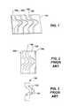
- FIG. 1a substrate 100 with a plurality of PLCs 102 thereon is shown. Referring to FIG.
- an OIC 120 diced using curvilinear cutting from a substrate containing a plurality of OICs thereonis shown (such as from the substrate shown in FIG. 1 ).
- an OIC 110 cut in a curvilinear manner from a substrateoften undesirably contains cracks 112 and chips 114 .
- Such cracks 112 and chips 114often constitute in fatal defects in the OIC 120 since the cracks 112 and chips 114 inhibit reliable operation of the optical components formed on the OIC.
- OIC substrates and the components thereonare often made of monocrystalline silicon, silicon dioxide, various oxides and silicates, and other materials that are very brittle by nature.
- the brittle nature of such materialsfacilitates the formation of cracks and chips in the substrate or the components thereon during cutting.
- the propensity to form cracks and chips during curvilinear cutting in combination with the brittle nature of the OIC substratesleads to the low yield of OICs from OIC substrates.
- since a plurality of OICsare fabricated in close proximity to one another, even small chips and cracks can render the OICs fatally defective.
- the present inventionprovides methods and OICs for facilitating curvilinear cutting of OICs substrate with high yield.
- the present inventionprovides methods and OICs for facilitating curvilinear cutting of OIC substrates while mitigating or eliminating edge chipping, cracking, and other degrading effects. In particular, providing waveguide stop cracks improves the cut quality of OICs.
- the present inventionmaximizes the yield of non-rectangular OICs from a single substrate.
- the present inventionalso correspondingly promotes maximizing the number of non-rectangular OICs that may be fabricated on a single substrate since isolation thereof in high yield is enabled.
- One aspect of the inventionrelates to a method of increasing optical integrated circuit yield per wafer, involving providing a wafer with a plurality of non-rectangular shaped optical integrated circuits; forming stop cracks in the wafer, each stop crack adjacent one of the non-rectangular shaped optical integrated circuits; cutting the wafer in a curvilinear manner to yield a plurality of separated non-rectangular shaped optical integrated circuits.
- Another aspect of the present inventionrelates to a method of dicing a substrate containing a plurality of non-rectangular shaped optical integrated circuits, involving forming stop cracks in the wafer, each stop crack adjacent and substantially parallel one of the non-rectangular shaped optical integrated circuits, and cutting the substrate in a curvilinear manner substantially parallel to a stop crack.
- Yet another aspect of the present inventionrelates to an optical structure containing a substrate; a plurality of non-rectangular shaped optical integrated circuits on the substrate, each non-rectangular shaped optical integrated circuit having an active region; and at least one stop crack positioned adjacent each non-rectangular shaped optical integrated circuit.
- Still yet another aspect of the inventionrelates to an optical integrated circuit containing a substrate having two curvilinear longitudinal edges, a non-rectangular shaped active region containing optical components, and at least one stop crack positioned substantially parallel and proximate one of the curvilinear longitudinal edges.
- FIG. 1illustrates a topdown view of an OIC substrate with a plurality of OICs thereon.
- FIG. 2illustrates a conventional manner of cutting an OIC substrate.
- FIG. 3illustrates problems with cutting an OIC substrate.
- FIG. 4illustrates OICs diced in accordance with one aspect of the present invention.
- FIG. 5illustrates an OIC diced in accordance with one aspect of the present invention.
- the present inventioninvolves forming stop cracks in an OIC substrate to facilitate curvilinear cutting of the OICs from a brittle substrate while minimizing/controlling chipping and cracking of the OIC and substrate.
- a substrate 100 with a plurality of PLCs 102 thereonis shown.
- all or substantially all of the individual PLCs 102may be cut and isolated from the substrate 100 with high yield. Curvilinear cutting between stop cracks is conducted to separate the non-rectangular shaped optical devices from each other while mitigating damage to the active region of the OICs.
- OIC 200in accordance with one aspect of the present invention is shown.
- OIC 200is non-rectangular in shape and has active region 202 where various optical components are positioned (such as lenses, taps, optical ports, waveguides, multiplexers, demultiplexers, AWGs, and the like), at least one and preferably two waveguide stop cracks 204 positioned substantially parallel with the longitudinal edge of the OIC, and sacrificial regions 206 positioned between the longitudinal edge and the waveguide stop cracks 204 .
- the stop cracks 204are positioned not only substantially parallel with the longitudinal edge of the OIC 200 , but also proximate the longitudinal edge of the OIC 200 to facilitate increased integration (maximizing the number of OICs formed on a given substrate).
- a substrateis fabricated with about 2 to about 50 OICs thereon.
- the presence of the waveguide stop cracks 204reduces the propensity of cracks 208 and chips from degrading the active region 202 of the OIC 200 .
- cracks 208 and chips created by curvilinear dicingdo not spread out of the sacrificial regions 206 into the active region 202 of the OIC 200 because the stop cracks 204 contain and/or isolate the cutting induced defects to the sacrificial regions 206 .
- the substrates with OICs thereon that are cut in accordance with the present inventionare made, at least in part, with brittle materials such as silica, monocrystalline silicon, silicon oxynitride, silicate glasses such as tetraethylorthosilicate (TEOS), organic/polymeric materials, and the like.
- silicate glassesinclude phosphosilicate glass (PSG), fluorosilicate glass (FSG), borophosphosilicate glass (BPSG) and borophosphotetraethylorthosilicate (BPTEOS).
- PSGphosphosilicate glass
- FSGfluorosilicate glass
- BPSGborophosphosilicate glass
- BPTEOSborophosphotetraethylorthosilicate
- the shape of the OICs on a given substrateis typically non-rectangular, but regular.
- a substrate with a plurality of OICsin the case PLCs, is shown.
- theymay be nested on the substrate to maximize the number of OICs fabricated on a given substrate.
- curvilinear cuttingmust be employed.
- the present inventionpermits curvilinear (a line that is curved, not straight) cutting of brittle materials.
- the stop crackis made in any suitable manner.
- the crackmay be formed using a saw, a milling machine, a laser, a water jet, or chemical etching.
- the stop cracksare made on the OICs at any time prior to dicing.
- the stop cracksmay be formed before, during or after optical components are provided in the active regions of the substrate.
- the stop crackmay remain empty after formation, or a material may be formed within the crack, such as providing silicon dioxide or other dielectric material in the crack.
- the stop crackmay thus be a trench or a layer of a stop crack material.
- the width of the stop crackis effective to deflect or prevent cracks and/or chips due to curvilinear cutting from propagating into the active region of the OIC.
- the width of the stop crackis about 1 micron or more and about 1 mm or less.
- the width of the stop crackis about 10 microns or more and about 0.5 mm or less.
- the width of the stop crackis about 25 microns or more and about 0.25 mm or less.
- the depth of the stop crackis effective to deflect or prevent cracks and/or chips due to curvilinear cutting from propagating into the active region of the OIC. In one embodiment, the depth of the stop crack is at least about 5% of the thickness of the OIC. In another embodiment, the depth of the stop crack is at least about 10% of the thickness of the OIC. In yet another embodiment, the depth of the stop crack is at least about 25% of the thickness of the OIC.
- the substrate containing a plurality of non-rectangular OICsis diced using curvilinear cutting to maximize the yield of non-rectangular OICs from the substrate.
- the substrateis cut by making the incision between stop cracks of adjacent OICs.
- the stop cracks of adjacent OICsare substantially parallel and the cut edge or incision is substantially parallel with the stop cracks.
- the substrateis diced in a curvilinear manner using any suitable cutting technique.
- the substratemay be diced using a saw, a milling machine, a laser, or a water jet.
- a componentis intended to refer to a computer-related entity, either hardware, a combination of hardware and software, software, or software in execution.
- a componentmay be, but is not limited to, a process running on a processor, a processor, an object, an executable, a thread of execution, a program, and a computer.
- the terms “includes”, “including”, “with”, “has”, “having”, and variants thereofare used in either the detailed description or the claims, these terms are intended to be inclusive in a manner similar to the term “comprising.”
Landscapes
- Physics & Mathematics (AREA)
- Engineering & Computer Science (AREA)
- Microelectronics & Electronic Packaging (AREA)
- General Physics & Mathematics (AREA)
- Optics & Photonics (AREA)
- Dicing (AREA)
Abstract
Description
Claims (15)
Priority Applications (1)
| Application Number | Priority Date | Filing Date | Title |
|---|---|---|---|
| US09/885,627US6895133B1 (en) | 2001-06-20 | 2001-06-20 | Crack propagation stops for dicing of planar lightwave circuit devices |
Applications Claiming Priority (1)
| Application Number | Priority Date | Filing Date | Title |
|---|---|---|---|
| US09/885,627US6895133B1 (en) | 2001-06-20 | 2001-06-20 | Crack propagation stops for dicing of planar lightwave circuit devices |
Publications (1)
| Publication Number | Publication Date |
|---|---|
| US6895133B1true US6895133B1 (en) | 2005-05-17 |
Family
ID=34574924
Family Applications (1)
| Application Number | Title | Priority Date | Filing Date |
|---|---|---|---|
| US09/885,627Expired - LifetimeUS6895133B1 (en) | 2001-06-20 | 2001-06-20 | Crack propagation stops for dicing of planar lightwave circuit devices |
Country Status (1)
| Country | Link |
|---|---|
| US (1) | US6895133B1 (en) |
Cited By (9)
| Publication number | Priority date | Publication date | Assignee | Title |
|---|---|---|---|---|
| US20040017974A1 (en)* | 2002-07-29 | 2004-01-29 | General Electric Company | Method and apparatus for fabricating waveguides and waveguides fabricated therefrom |
| US20090203192A1 (en)* | 2008-02-13 | 2009-08-13 | Erdem Kaltalioglu | Crack Stop Trenches |
| US20110138860A1 (en)* | 2008-05-19 | 2011-06-16 | Martin Armani Andrea | Silica-on-silicon waveguides and related fabrication methods |
| US8917444B2 (en) | 2011-06-17 | 2014-12-23 | California Institute Of Technology | Chip-based frequency comb generator with microwave repetition rate |
| US9293887B2 (en) | 2011-06-17 | 2016-03-22 | California Institute Of Technology | Chip-based laser resonator device for highly coherent laser generation |
| US9537571B2 (en) | 2014-01-24 | 2017-01-03 | California Institute Of Technology | Dual-frequency optical source |
| US9595918B2 (en) | 2014-03-06 | 2017-03-14 | California Institute Of Technology | Stable microwave-frequency source based on cascaded brillouin lasers |
| US9905999B2 (en) | 2015-02-26 | 2018-02-27 | California Institute Of Technology | Optical frequency divider based on an electro-optical-modulator frequency comb |
| US20230152539A1 (en)* | 2020-03-31 | 2023-05-18 | Sumitomo Osaka Cement Co., Ltd. | Optical waveguide element, and optical modulation device and optical transmission device using same |
Citations (8)
| Publication number | Priority date | Publication date | Assignee | Title |
|---|---|---|---|---|
| US4610079A (en)* | 1980-01-22 | 1986-09-09 | Tokyo Shibaura Denki Kabushiki Kaisha | Method of dicing a semiconductor wafer |
| US5447585A (en) | 1991-11-25 | 1995-09-05 | Corning Incorporated | Method of manufacturing and testing integrated optical components |
| US5789302A (en)* | 1997-03-24 | 1998-08-04 | Siemens Aktiengesellschaft | Crack stops |
| US5872883A (en) | 1995-11-28 | 1999-02-16 | Mitsubishi Gas Chemical Company, Inc. | Curved optical waveguide and method of manufacturing the same |
| US5926586A (en) | 1997-07-09 | 1999-07-20 | Lucent Technologies Inc. | Non-rectangular optical devices |
| US6219471B1 (en) | 1999-01-15 | 2001-04-17 | Lucent Technologies Inc. | Optical device having equal length waveguide paths |
| US6407360B1 (en)* | 1998-08-26 | 2002-06-18 | Samsung Electronics, Co., Ltd. | Laser cutting apparatus and method |
| US6495918B1 (en)* | 2000-09-05 | 2002-12-17 | Infineon Technologies Ag | Chip crack stop design for semiconductor chips |
- 2001
- 2001-06-20USUS09/885,627patent/US6895133B1/ennot_activeExpired - Lifetime
Patent Citations (8)
| Publication number | Priority date | Publication date | Assignee | Title |
|---|---|---|---|---|
| US4610079A (en)* | 1980-01-22 | 1986-09-09 | Tokyo Shibaura Denki Kabushiki Kaisha | Method of dicing a semiconductor wafer |
| US5447585A (en) | 1991-11-25 | 1995-09-05 | Corning Incorporated | Method of manufacturing and testing integrated optical components |
| US5872883A (en) | 1995-11-28 | 1999-02-16 | Mitsubishi Gas Chemical Company, Inc. | Curved optical waveguide and method of manufacturing the same |
| US5789302A (en)* | 1997-03-24 | 1998-08-04 | Siemens Aktiengesellschaft | Crack stops |
| US5926586A (en) | 1997-07-09 | 1999-07-20 | Lucent Technologies Inc. | Non-rectangular optical devices |
| US6407360B1 (en)* | 1998-08-26 | 2002-06-18 | Samsung Electronics, Co., Ltd. | Laser cutting apparatus and method |
| US6219471B1 (en) | 1999-01-15 | 2001-04-17 | Lucent Technologies Inc. | Optical device having equal length waveguide paths |
| US6495918B1 (en)* | 2000-09-05 | 2002-12-17 | Infineon Technologies Ag | Chip crack stop design for semiconductor chips |
Cited By (16)
| Publication number | Priority date | Publication date | Assignee | Title |
|---|---|---|---|---|
| US20040017974A1 (en)* | 2002-07-29 | 2004-01-29 | General Electric Company | Method and apparatus for fabricating waveguides and waveguides fabricated therefrom |
| US6957007B2 (en)* | 2002-07-29 | 2005-10-18 | General Electric Company | Method and apparatus for fabricating waveguides and waveguides fabricated therefrom |
| US7146081B2 (en) | 2002-07-29 | 2006-12-05 | General Electric Company | Waveguide including a plurality of waveguide segments |
| US8610238B2 (en) | 2008-02-13 | 2013-12-17 | Infineon Technologies Ag | Crack stop trenches |
| US7871902B2 (en) | 2008-02-13 | 2011-01-18 | Infineon Technologies Ag | Crack stop trenches |
| US20110074033A1 (en)* | 2008-02-13 | 2011-03-31 | Erdem Kaltalioglu | Crack Stop Trenches |
| US20090203192A1 (en)* | 2008-02-13 | 2009-08-13 | Erdem Kaltalioglu | Crack Stop Trenches |
| US20110138860A1 (en)* | 2008-05-19 | 2011-06-16 | Martin Armani Andrea | Silica-on-silicon waveguides and related fabrication methods |
| US8094987B2 (en)* | 2008-05-19 | 2012-01-10 | California Institute Of Technology | Silica-on-silicon waveguides and related fabrication methods |
| US8917444B2 (en) | 2011-06-17 | 2014-12-23 | California Institute Of Technology | Chip-based frequency comb generator with microwave repetition rate |
| US9293887B2 (en) | 2011-06-17 | 2016-03-22 | California Institute Of Technology | Chip-based laser resonator device for highly coherent laser generation |
| US9537571B2 (en) | 2014-01-24 | 2017-01-03 | California Institute Of Technology | Dual-frequency optical source |
| US10009103B2 (en) | 2014-01-24 | 2018-06-26 | California Institute Of Technology | Stabilized microwave-frequency source |
| US9595918B2 (en) | 2014-03-06 | 2017-03-14 | California Institute Of Technology | Stable microwave-frequency source based on cascaded brillouin lasers |
| US9905999B2 (en) | 2015-02-26 | 2018-02-27 | California Institute Of Technology | Optical frequency divider based on an electro-optical-modulator frequency comb |
| US20230152539A1 (en)* | 2020-03-31 | 2023-05-18 | Sumitomo Osaka Cement Co., Ltd. | Optical waveguide element, and optical modulation device and optical transmission device using same |
Similar Documents
| Publication | Publication Date | Title |
|---|---|---|
| US7049672B2 (en) | Method and apparatus for preparing a plurality of dice in wafers | |
| EP2962139B1 (en) | Photonic device structure and method of manufacture | |
| US5418190A (en) | Method of fabrication for electro-optical devices | |
| US6895133B1 (en) | Crack propagation stops for dicing of planar lightwave circuit devices | |
| CN101071790A (en) | Semiconductor substrate, and semiconductor device and method of manufacturing the semiconductor device | |
| US11506840B2 (en) | Back end of line process integrated optical device fabrication | |
| JPH01120885A (en) | Method of cutting off laser diodes formed in monolithic form | |
| US20110135265A1 (en) | Method of forming waveguide facet and photonics device using the method | |
| US6335559B1 (en) | Semiconductor device cleave initiation | |
| US6955989B2 (en) | Use of a U-groove as an alternative to using a V-groove for protection against dicing induced damage in silicon | |
| US20090134496A1 (en) | Wafer and method of forming alignment markers | |
| US20050284181A1 (en) | Method for making an optical waveguide assembly with integral alignment features | |
| US5926586A (en) | Non-rectangular optical devices | |
| US20030021572A1 (en) | V-groove with tapered depth and method for making | |
| US7267780B1 (en) | Formation of facets on optical components | |
| JP5545648B2 (en) | Cleaving method of semiconductor wafer | |
| US7257304B2 (en) | Integrated optical device with reduced waveguide birefringence | |
| US7224870B2 (en) | Method of coupling fiber to waveguide | |
| JP2000031115A (en) | Method for forming chip from wafer | |
| JP2940602B2 (en) | Optical component fixing board | |
| WO2003044841A2 (en) | Method of dicing a complex topologically structured wafer | |
| WO1998022841A1 (en) | Process to create the coupling in an optoelectronic device between an optical fiber and a waveguide and device obtained from this process | |
| WO2003034115A2 (en) | Coupling a semiconducter laser to an optical waveguide | |
| JPH11204463A (en) | Semiconductor chip cutting-off method |
Legal Events
| Date | Code | Title | Description |
|---|---|---|---|
| AS | Assignment | Owner name:LIGHTWAVE MICROSYSTEMS, CALIFORNIA Free format text:ASSIGNMENT OF ASSIGNORS INTEREST;ASSIGNORS:CALKINS, CHRIS P.;COLE, ROBERT;REEL/FRAME:011924/0246;SIGNING DATES FROM 20010619 TO 20010620 | |
| AS | Assignment | Owner name:LIGHTWAVE MICROSYSTEM CORPORATION, CALIFORNIA Free format text:CORRECTIVE ASSIGNMENT TO CORRECT THE NAME AND THE STREET ADDRESS OF THE ASSIGNEE PREVIOUSLY RECORDED AT REEL 011924, FRAME 0246;ASSIGNORS:CALKINS, CHRIS P.;COLE, ROBERT;REEL/FRAME:012637/0373;SIGNING DATES FROM 20010919 TO 20010920 | |
| STCF | Information on status: patent grant | Free format text:PATENTED CASE | |
| REMI | Maintenance fee reminder mailed | ||
| FEPP | Fee payment procedure | Free format text:PAT HOLDER NO LONGER CLAIMS SMALL ENTITY STATUS, ENTITY STATUS SET TO UNDISCOUNTED (ORIGINAL EVENT CODE: STOL); ENTITY STATUS OF PATENT OWNER: LARGE ENTITY | |
| FPAY | Fee payment | Year of fee payment:4 | |
| SULP | Surcharge for late payment | ||
| AS | Assignment | Owner name:NEOPHOTONICS CORPORATION,CALIFORNIA Free format text:ASSIGNMENT OF ASSIGNORS INTEREST;ASSIGNOR:LIGHTWAVE MICROSYSTEMS CORPORATION;REEL/FRAME:024505/0068 Effective date:20100608 Owner name:NEOPHOTONICS CORPORATION, CALIFORNIA Free format text:ASSIGNMENT OF ASSIGNORS INTEREST;ASSIGNOR:LIGHTWAVE MICROSYSTEMS CORPORATION;REEL/FRAME:024505/0068 Effective date:20100608 | |
| FPAY | Fee payment | Year of fee payment:8 | |
| FEPP | Fee payment procedure | Free format text:PAYOR NUMBER ASSIGNED (ORIGINAL EVENT CODE: ASPN); ENTITY STATUS OF PATENT OWNER: LARGE ENTITY | |
| FPAY | Fee payment | Year of fee payment:12 |