US6895089B2 - Pots splitter with line impedance matching - Google Patents
Pots splitter with line impedance matchingDownload PDFInfo
- Publication number
- US6895089B2 US6895089B2US10/017,353US1735301AUS6895089B2US 6895089 B2US6895089 B2US 6895089B2US 1735301 AUS1735301 AUS 1735301AUS 6895089 B2US6895089 B2US 6895089B2
- Authority
- US
- United States
- Prior art keywords
- differential mode
- mode inductor
- winding
- parallel
- capacitor
- Prior art date
- Legal status (The legal status is an assumption and is not a legal conclusion. Google has not performed a legal analysis and makes no representation as to the accuracy of the status listed.)
- Expired - Lifetime, expires
Links
- 239000003990capacitorSubstances0.000claimsabstractdescription166
- 238000004804windingMethods0.000claimsdescription238
- 230000008878couplingEffects0.000claimsdescription26
- 238000010168coupling processMethods0.000claimsdescription26
- 238000005859coupling reactionMethods0.000claimsdescription26
- 238000000034methodMethods0.000claimsdescription13
- 238000012546transferMethods0.000description6
- 230000005540biological transmissionEffects0.000description5
- 238000003780insertionMethods0.000description5
- 230000037431insertionEffects0.000description5
- 238000010586diagramMethods0.000description4
- 230000006978adaptationEffects0.000description2
- 239000000969carrierSubstances0.000description2
- 238000004891communicationMethods0.000description2
- 238000013461designMethods0.000description2
- 239000007787solidSubstances0.000description2
- 230000001629suppressionEffects0.000description2
- 230000003247decreasing effectEffects0.000description1
- 238000001914filtrationMethods0.000description1
- 238000012986modificationMethods0.000description1
- 230000004048modificationEffects0.000description1
- 230000001131transforming effectEffects0.000description1
Images


Classifications
- H—ELECTRICITY
- H04—ELECTRIC COMMUNICATION TECHNIQUE
- H04M—TELEPHONIC COMMUNICATION
- H04M1/00—Substation equipment, e.g. for use by subscribers
- H04M1/738—Interface circuits for coupling substations to external telephone lines
- H04M1/76—Compensating for differences in line impedance
Definitions
- the present inventionrelates generally to telecommunications, and in particular to apparatus and methods to facilitate line impedance matching in a POTS splitter.
- a variety of telecommunication systemsutilize traditional telephone company local subscriber loops to carry high rate digital transmissions. Examples include a variety of digital subscriber loop (DSL) services, such as high-rate DSL (HDSL), asymmetric DSL (ADSL), very high-rate DSL (VDSL) and others.
- DSLdigital subscriber loop
- HDSLhigh-rate DSL
- ADSLasymmetric DSL
- VDSLvery high-rate DSL
- xDSLThe varieties of DSL service will be referred to herein generally as xDSL.
- POTSplain old telephone service
- FDMfrequency division multiplexing
- a splitteror POTS splitter
- These splittersgenerally have a low-pass filter to permit passing of the POTS service and a high-pass filter to permit passing of the xDSL service.
- the POTS splittermust have its impedance matched to the transmission line or carrier.
- the various embodimentsutilize resistance in parallel with the inductors in a series leg of the low-pass filter.
- This parallel resistancefacilitates changes input and output resistance of the filter with little or no change in the reactance of the inductors.
- the reactance of the capacitors in the shunt legs of the filterwill be substantially unaffected. This assists the designer in matching the impedance of the filter in the pass-band while still providing substantial impedance mismatching in the stop-band without substantially affecting the characteristics of the filter.
- Facilitating impedance matching in the pass-band and impedance mismatching in the stop-bandis accomplished without the need for more complex active components.
- Various embodimentsmay further contain additional components that do not materially affect the basic and novel properties of the devices disclosed herein.
- the inventionprovides a low-pass filter.
- the filterincludes a first differential mode inductor in series with a second differential mode inductor, first and second resistors in parallel with the first differential mode inductor, third and fourth resistors in parallel with the second differential mode inductor, a first capacitor in parallel with the third resistor, and a second capacitor in parallel with the fourth resistor.
- the filterfurther includes a first shunt leg interposed between the first and second differential mode inductors and coupled across the first and second differential mode inductors and a second shunt leg.
- the second differential mode inductoris interposed between the first and second shunt legs.
- the low-pass filteris a passive low-pass filter.
- a common mode inductoris coupled between the second shunt leg and the second differential mode inductor.
- the inventionprovides a low-pass filter.
- the filterincludes a first differential mode inductor in series with a second differential mode inductor, a first resistor in parallel with a first winding of the first differential mode inductor, a second resistor in parallel with a second winding of the first differential mode inductor, a third resistor in parallel with a first winding of the second differential mode inductor, a fourth resistor in parallel with a second winding of the second differential mode inductor, a first capacitor in parallel with the first winding of the second differential mode inductor, and a second capacitor in parallel with the second winding of the second differential mode inductor.
- the filterfurther includes a first shunt leg comprising a first end coupled between the first windings of the first and second differential mode inductors and a second end coupled between the second windings of the first and second differential mode inductors.
- the filterstill further includes a second shunt leg comprising a first end coupled to the first winding of the second differential mode inductor and a second end coupled to the second winding of the second differential mode inductor.
- the second differential mode inductoris coupled between the first and second shunt legs.
- a common mode inductoris coupled between the second shunt leg and the second differential mode inductor.
- the inventionprovides a low-pass filter.
- the filterincludes a first differential mode inductor in series with a second differential mode inductor, a first resistor in parallel with a first winding of the first differential mode inductor, a second resistor in parallel with a second winding of the first differential mode inductor, a third resistor in parallel with a first winding of the second differential mode inductor, a fourth resistor in parallel with a second winding of the second differential mode inductor, a first capacitor in parallel with the first winding of the second differential mode inductor and the third resistor, and a second capacitor in parallel with the second winding of the second differential mode inductor and the fourth resistor.
- the filterfurther includes a first shunt leg comprising a first end coupled between the first windings of the first and second differential mode inductors and a second end coupled between the second windings of the first and second differential mode inductors.
- the filterstill further includes a second shunt leg.
- the second differential mode inductoris coupled between the first and second shunt legs.
- a common mode inductoris coupled between the second shunt leg and the second differential mode inductor.
- the inventionprovides a POTS splitter.
- the splitterincludes a high-pass filter for coupling between an xDSL in port and an xDSL out port and a low-pass filter for coupling between the xDSL out port and a POTS port.
- the low-pass filterincludes a first differential mode inductor in series with a second differential mode inductor between the POTS port and the xDSL out port, first and second resistors in parallel with the first differential mode inductor, third and fourth resistors in parallel with the second differential mode inductor, a first capacitor in parallel with the third resistor, a second capacitor in parallel with the fourth resistor, a first shunt leg interposed between the first and second differential mode inductors and coupled across the first and second differential mode inductors, and a second shunt leg coupled across the second differential mode inductor.
- the inventionprovides telecommunications system.
- the systemincludes a carrier, a high-pass filter coupled between the carrier and an xDSL transceiver, and a low-pass filter coupled between the carrier and a POTS transceiver.
- the low-pass filterincludes a first differential mode inductor in series with a second differential mode inductor between the POTS transceiver and the carrier, first and second resistors in parallel with the first differential mode inductor, third and fourth resistors in parallel with the second differential mode inductor, a first capacitor in parallel with the third resistor, a second capacitor in parallel with the fourth resistor, a first shunt leg interposed between the first and second differential mode inductors and coupled across the first and second differential mode inductors, and a second shunt leg coupled across the second differential mode inductor.
- a common mode inductoris coupled between the second shunt leg and the second differential mode inductor.
- the inventionprovides a method of impedance matching in a POTS splitter of a telecommunications system for sharing a common carrier between xDSL service and POTS service.
- the methodincludes passing a first signal on a tip line between a POTS transceiver and the carrier, wherein the first signal passes through a first winding of a first differential mode inductor and a first winding of a second differential mode inductor in series while a first resistance is in parallel with the first winding of the first differential mode inductor, a second resistance is in parallel with the first winding of the second differential mode inductor and a first capacitance is in parallel with the first winding of the second differential mode inductor and the second resistance.
- the methodfurther includes passing a second signal on a ring line between a POTS transceiver and the carrier, wherein the second signal passes through a second winding of the first differential mode inductor and a second winding of the second differential mode inductor in series while a third resistance is in parallel with the second winding of the first differential mode inductor, a fourth resistance is in parallel with the second winding of the second differential mode inductor and a second capacitance is in parallel with the second winding of the second differential mode inductor and the fourth resistance.
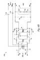
- FIG. 1is a block diagram of a communication network having a POTS splitter in accordance with an embodiment of the invention.
- FIG. 2is a block diagram of a POTS splitter showing additional detail on the connections between the various carriers in accordance with an embodiment of the invention.
- FIG. 3is a graph depicting the pass-bands and stop-band generally used for a POTS splitter.
- FIGS. 4A-4Bare schematics of POTS splitters in accordance with embodiments of the invention.
- FIGS. 5A-5Bare graphs showing equivalent series resistance of an inductor having parallel resistors for use with embodiments of the invention.
- Impedance matchingis necessary in the design of POTS splitters to provide the maximum possible transfer of signal power between a source and its load. Mismatched impedance in the transmission line can cause signal reflection, echo return and power loss.
- the maximum transfer power of a signal, from a source to its load,occurs when load impedance is equal to the complex conjugate of the source impedance. In other words, the impedance of source and load have the same real part and opposite reactance.
- the designergenerally does not have the ability to change the filter input and output impedance by changing the values of impedance (L) and capacitance (C) when the coefficient of the filter is calculated. Changing the values of L and C in the filter will change the cutoff frequency and attenuation of frequency response of the filter. Modifications of the input and output impedance can be accomplished using active filtering, but such complexity can lead to higher failure rates of installed splitters. Moreover, the use of active circuits in the filter can interfere with lifeline POTS support. Such lifeline POTS service is generally required by telephony companies for emergency access of the telecommunications system.
- filter impedanceis modified by adding parallel resistors with the inductors in the series leg of the filter. This changes input and output resistance of a filter without changing the reactance of the inductors in the series leg if the quality, Q, is greater than 10. If Q is less than 10, reactance of the inductors will see little change. Furthermore, the reactance of the capacitors in the shunt legs of the filter will be substantially unaffected. Therefore, it will generally not change the characteristics of the filter to add parallel resistors to the inductors.
- the various embodimentshelp facilitate impedance matching in a POTS splitter for the pass-band of the low-pass filter portion while facilitating impedance mismatching in the stop-band of the low-pass filter.
- Various embodimentsinclude two pairs of resistors in parallel with differential mode inductors in a fourth-order low-pass filter. By transforming a parallel circuit into the equivalent series resistor and inductance circuit, several tens of ohms resistance can be added to the splitter in the pass-band to improve line impedance matching and several kilo-ohms resistance can be added to the splitter in the stop-band to accelerate the impedance mismatching. The circuit sees an effective filter resistance that is larger than what is actually present.
- FIG. 1is a block diagram of a communication network 100 having a POTS splitter 101 coupled between a customer loop, or local loop carrier, and a central office (CO) POTS transceiver and DSL transceiver, such as a DSL access multiplexer (DSLAM) ADSL transceiver unit (ATU).
- the primary components of the POTS splitter 101include the CO POTS low-pass filter and the RC high-pass filter.
- the POTS splitter 101would contain only the capacitive portion of the high-pass filter, relying on modem circuitry to provide the resistive portion. Additional circuitry may include overvoltage and surge protection, a loop present indicator and a signature resistance.
- the POTS splitter 101includes a low-pass filter in accordance with an embodiment of the invention.
- FIG. 2is a block diagram of a POTS splitter 101 showing additional detail on the connections between the various carriers.
- the POTS splitter 101 of FIG. 2includes a low-pass filter 205 , in accordance with an embodiment of the invention, having a tip line from the CO coupled to a tip line of the local loop and a ring line from the CO coupled to a ring line of the local loop.
- the POTS splitter 101 of FIG. 2further includes a tip line from the CO ATU coupled to the tip line of the local loop and a ring line from the CO ATU coupled to the ring line of the local loop.
- the tip and ring linesgenerally present a characteristic impedance of approximately 900 ⁇ for incoming signals and approximately 600 ⁇ or less for the return signals.
- the ATUwill typically present a characteristic impedance of approximately 100 ⁇ .
- FIG. 3is a graph depicting the pass-bands and stop-band generally used for a POTS splitter 101 .
- the low-pass filterhas a pass-band of approximately 0-4 kHz while the high-pass filter has a pass-band of approximately 32 kHz and above.
- the stop-band for the low-pass filteris generally anything above its pass-band, particularly 32 kHz or above, while the stop-band for the high-pass filter is generally anything below its pass-band, particularly 4 kHz or below.
- FIG. 4Ais a schematic of a POTS splitter 101 A in accordance with an embodiment of the invention.
- the POTS splitter 101 A of FIG. 4Aincludes a high-pass filter including capacitors C 101 and C 102 coupled between the ring and tip lines, respectively, of an xDSL in port, e.g., the CO ATU or other DSL transceiver, and an xDSL out port, e.g., the local loop.
- the high-pass filtercan further include resistive components (not shown) in an associated modem circuit.
- the POTS splitter 101 Amay further include a solid state voltage suppressor 115 or other over-voltage suppression circuitry coupled between the ring and tip lines of the xDSL out port.
- the POTS splitter 101 Amay include circuitry 120 coupled between the ring and tip lines of a POTS port, e.g., a CO POTS transceiver, for providing loop presence indication and signature resistance.
- the circuitry 120includes series-connected diode CR 2 , zener diode or regulator CR 3 and resistor R 5 . Fuses F 1 and F 2 may be inserted in the tip and ring lines, respectively, for further surge protection. For example, F 1 and F 2 may represent 1.5 A fuses.
- the POTS splitter 101 A of FIG. 4Afurther includes a low-pass filter including series-connected differential mode inductors T 1 and T 2 .
- the inductor T 1has a higher inductance than the inductor T 2 .
- the inductors T 1 and T 2have inductance values in the range of approximately 5 mH to approximately 25 mH.
- the inductor T 1has an inductance of approximately 22 mH while the inductor T 2 has an inductance of 8 mH.
- the low-pass filteris a fourth-order elliptic low-pass filter.
- Inductor T 1is further coupled to resistors R 1 and R 2 , which are coupled across the tip lines and ring lines, respectively.
- the resistors R 1 and R 2are in parallel with separate windings of the inductor T 1 .
- Inductor T 2is further coupled to resistors R 3 and R 4 , which are coupled across the tip lines and ring lines, respectively.
- the resistors R 3 and R 4are in parallel with separate windings of the inductor T 2 .
- Inductor T 2is still further coupled to capacitors C 3 and C 4 , which are coupled across the tip lines and ring lines, respectively.
- the capacitors C 3 and C 4are in parallel with the resistors R 3 and R 4 , respectively.
- the resistors R 1 , R 2 , R 3 and R 4are used to fine tune the filter resistance to improve impedance matching with line and load termination.
- the parallel resistor R 1 and the parallel resistor R 2have substantially the same resistance.
- the parallel resistor R 3 and the parallel resistor R 4have substantially the same resistance.
- the parallel resistors R 1 and R 2each have a lower resistance value than the parallel resistors R 3 and R 4 .
- the parallel resistors R 1 and R 2have resistance values greater than approximately 1 k ⁇ .
- the parallel resistors R 1 and R 2further have resistance values less than approximately 5 k ⁇ .
- the parallel resistors R 3 and R 4have resistance values greater than approximately 5 k ⁇ .
- the parallel resistors R 3 and R 4further have resistance values less than or equal to approximately 30 k ⁇ .
- parallel resistors R 1 and R 2may have resistance values of approximately 3.01 k ⁇ and the parallel resistors R 3 and R 4 may have resistance values of approximately 5.62 k ⁇ .
- the parallel capacitors C 3 and C 4have substantially the same capacitance.
- the parallel capacitors C 3 and C 4have capacitance values greater than approximately 0.002 ⁇ F.
- the parallel capacitors C 3 and C 4further have capacitance values less than approximately 0.006 ⁇ F.
- parallel capacitors C 3 and C 4may have capacitance values of approximately 0.0056 ⁇ F.
- Shunt legsmay be inserted between the tip and ring lines of the low-pass filter.
- shunt capacitor C 1may be interposed between the inductor T 1 and the inductor T 2 and coupled between the tip and ring lines, e.g., between the separate windings of the inductors T 1 and T 2 .
- a resistor R 6may be coupled between the tip and ring lines in series with the capacitor C 1 .
- Such resistanceis preferable when attempting to match the complex impedance of a European POTS system.
- shunt capacitor C 2may be interposed between the inductor T 2 and the POTS port and coupled between the tip and ring lines, e.g., between the windings of the inductor T 2 .
- a resistor R 7may be coupled between the tip and ring lines in series with the capacitor C 2 . Series resistance with the shunt capacitors is preferable when attempting to match the complex impedance of a European telephony system.
- the first shunt legi.e., C 1 /R 6
- the capacitor C 1has a lower capacitance than the capacitor C 2 .
- the capacitors C 1 and C 2have capacitance values of approximately 0.01 ⁇ F or greater.
- the capacitors C 1 and C 2have capacitance values of approximately 0.07 ⁇ F or less.
- the resistors R 6 and R 7have resistance values of approximately 70 ⁇ or less.
- capacitor C 1may have a capacitance value of approximately 0.027 ⁇ F and the capacitor C 2 may have a capacitance value of approximately 0.051 ⁇ F.
- the resistors R 6 and R 7may be in the range of approximately 20-70 ⁇ .
- the resistors R 6 and R 7may have resistance values of approximately 20 ⁇ .
- POTS terminalsmay produce common mode impulses which will pass through a differential mode filter and cause errors in the DSL modem. This may happen when going “on/off hook.” POTS line cards may further produce them at the start/stop of the ringing cadence.
- Another source of troublesome common mode signalcan be from switched mode power supplies as typically used in fax machines and laptop computers.
- a common mode filtercan be used to help alleviate these problems.
- the POTS splitter 101 Aincludes a common mode inductor T 3 coupled between the POTS port and the xDSL out port, e.g., between the second shunt leg and the inductor T 2 .
- the inductor T 3has a first winding corresponding to the tip line and a second winding corresponding to the ring line.
- the common mode inductor T 3should be constructed such that the resonance between its inductance and interwinding capacitance is placed in the middle of the DSL band.
- the inductor T 3has an inductance value of approximately 10 mH.
- FIG. 4Bis a schematic of a POTS splitter 101 B in accordance with an embodiment of the invention.
- the POTS splitter 101 B of FIG. 4Bincludes a high-pass filter including capacitors C 101 and C 102 coupled between the ring and tip lines, respectively, of an xDSL in port, e.g., the CO ATU or other DSL transceiver, and an xDSL out port, e.g., the local loop.
- the POTS splitter 101 Bmay further include a solid state voltage suppressor 115 or other over-voltage suppression circuitry coupled between the ring and tip lines of the xDSL out port.
- the POTS splitter 101 Bmay include circuitry 120 coupled between the ring and tip lines of a POTS port, e.g., a CO POTS transceiver, for providing loop presence indication and signature resistance.
- the circuitry 120includes series-connected diode CR 2 , zener diode or regulator CR 3 and resistor R 5 . Fuses F 1 and F 2 may be inserted in the tip and ring lines, respectively, for further surge protection. For example, F 1 and F 2 may represent 1.5 A fuses.
- the POTS splitter 101 B of FIG. 4Bfurther includes a low-pass filter including series-connected differential mode inductors T 1 and T 2 .
- the inductor T 1has a higher inductance than the inductor T 2 .
- the inductors T 1 and T 2have inductance values in the range of approximately 5 mH to approximately 25 mH.
- the inductors T 1 and T 2each have an inductance of approximately 21 mH.
- the low-pass filteris a fourth-order elliptic low-pass filter.
- Inductor T 1is further coupled to resistors R 1 and R 2 , which are coupled across the tip lines and ring lines, respectively.
- the resistors R 1 and R 2are in parallel with separate windings of the inductor T 1 .
- Inductor T 2is further coupled to resistors R 3 and R 4 , which are coupled across the tip lines and ring lines, respectively.
- the resistors R 3 and R 4are in parallel with separate windings of the inductor T 2 .
- Inductor T 2is still further coupled to capacitors C 3 and C 4 , which are coupled across the tip lines and ring lines, respectively.
- the capacitors C 3 and C 4are in parallel with the resistors R 3 and R 4 , respectively.
- the resistors R 1 , R 2 , R 3 and R 4are used to fine tune the filter resistance to improve impedance matching with line and load termination.
- the parallel resistor R 1 and the parallel resistor R 2have substantially the same resistance.
- the parallel resistor R 3 and the parallel resistor R 4have substantially the same resistance.
- the parallel resistors R 1 and R 2each have a lower resistance value than the parallel resistors R 3 and R 4 .
- the parallel resistors R 1 and R 2have resistance values greater than approximately 1 k ⁇ .
- the parallel resistors R 1 and R 2further have resistance values less than approximately 5 k ⁇ .
- the parallel resistors R 3 and R 4have resistance values greater than approximately 5 k ⁇ .
- the parallel resistors R 3 and R 4further have resistance values less than or equal to approximately 30 k ⁇ .
- parallel resistors R 1 and R 2may have resistance values in the range of approximately 4.75 k ⁇ to approximately 5.11 k ⁇ and the parallel resistors R 3 and R 4 may have resistance values in the range of approximately 15 k ⁇ to approximately 30.1 k ⁇ .
- parallel resistors R 1 and R 2may have resistance values of approximately 4.75 k ⁇ and the parallel resistors R 3 and R 4 may have resistance values of approximately 15 k ⁇ .
- parallel resistors R 1 and R 2may have resistance values of approximately 5.11 k ⁇ and the parallel resistors R 3 and R 4 may have resistance values of approximately 30.1 k ⁇ .
- the parallel capacitors C 3 and C 4have substantially the same capacitance.
- the parallel capacitors C 3 and C 4have capacitance values greater than approximately 0.002 ⁇ F.
- the parallel capacitors C 3 and C 4further have capacitance values less than approximately 0.006 ⁇ F.
- parallel capacitors C 3 and C 4may have capacitance values of approximately 0.0022 ⁇ F.
- Shunt legsmay be inserted between the tip and ring lines of the low-pass filter.
- shunt capacitor C 1may be interposed between the inductor T 1 and the inductor T 2 and coupled between the tip and ring lines, e.g., between the separate windings of the inductors T 1 and T 2 .
- shunt capacitor C 2may be interposed between the inductor T 2 and the POTS port and coupled between the tip and ring lines, e.g., between the windings of the inductor T 2 .
- the shunt legs of the POTS splitter 101 B of FIG. 4Bdepict that the resistance in series with the shunt capacitors may be eliminated.
- the first shunt legi.e., C 1
- the capacitor C 1has a lower RC constant than the second shunt leg, i.e., C 2 .
- the capacitor C 1has a lower capacitance than the capacitor C 2 .
- the capacitors C 1 and C 2have capacitance values of approximately 0.01 ⁇ F or greater.
- the capacitors C 1 and C 2have capacitance values of approximately 0.07 ⁇ F or less. In one example embodiment, e.g., for a North America application, capacitor C 1 may have a capacitance value of approximately 0.01 ⁇ F and the capacitor C 2 may have a capacitance value of approximately 0.068 ⁇ F.
- mismatched impedance in the transmission linecauses signal reflection, echo return and power loss.
- the maximum transfer of power of a signal from a source to its loadoccurs when load impedance is equal to the complex conjugate of the source impedance.
- the impedance of the source and loadshould have the same real part and opposite reactance.
- the POTS splittergenerally needs to pass frequencies up to 3.4 kHz with less than 0.75 dB for long loop and 1.00 dB for short loop insertion loss at 1 kHz and to attenuate at least 65 dB at a frequency range of 32 kHz to 300 kHz and 55 dB at a frequency range of 300 kHz to 1104 kHz according to the ANSI T1.413 standard.
- Such standardsalso require voice band attenuation at 0.2 to 3.4 kHz of +1.5 dB to ⁇ 1.5 dB for short loop and of +0.5 dB to ⁇ 1.5 dB for long loop.
- Such standardsalso require voice band attenuation at 3.4 to 4 kHz of +2.0 dB to ⁇ 2.0 dB for short loop and of +1.0 dB to ⁇ 1.5 dB for long loop. Attenuation should be greater than 8 dB for echo return loss (ERL), and be greater than 5 dB for both singing return loss low (SRL-L) and singing return loss high (SRL-H).
- ERPecho return loss
- SRL-Lsinging return loss low
- SRL-Hsinging return loss high
- the POTS splittergenerally needs to pass frequencies up to 3.4 kHz with less than 1 dB for insertion loss at 1 kHz and to attenuate at least 55 dB at frequencies 32 kHz and above according to the standard ETSI TR 101 728 V1.1.1.
- the absolute difference between the insertion loss at any frequency in the range 200 Hz to 4 kHz and the insertion loss at 1 kHzshall be less than 1 dB according to the standard.
- Attenuation of Return Lossshall be greater than 12 dB at a frequency range of 300 Hz to 3400 Hz and 8 dB at 3400 Hz to 4000 Hz. A value of 14 dB for the minimum Return Loss instead of 12 dB is desirable.
- FIG. 5Ais a graph showing an equivalent series resistance, Rst 1 , of the first inductor T 1 with parallel resistors R 1 and R 2 as a function of frequency, fc.
- This graphrepresents the expected equivalent series resistance of 9.5 k ⁇ in parallel with a 21 mH inductor, e.g., two 4.75 k ⁇ resistors in parallel with a 21 mH inductor having a winding resistance of approximately 9 ⁇ .
- Rst 1is approximately 10.7 ⁇ at 1 kHz, 38.1 ⁇ at 4 kHz, and 1.57 k ⁇ at 32 kHz.
- FIG. 5Ais a graph showing an equivalent series resistance, Rst 1 , of the first inductor T 1 with parallel resistors R 1 and R 2 as a function of frequency, fc.
- This graphrepresents the expected equivalent series resistance of 9.5 k ⁇ in parallel with a 21 mH inductor, e.g., two 4.75 k ⁇ resistors in parallel with a 21 m
- 5Bis a graph showing an equivalent series resistance, Rst 2 , of the second inductor T 2 with parallel resistors R 3 and R 4 as a function of frequency, fc.
- This graphrepresents the expected equivalent series resistance of 30 k ⁇ in parallel with a 21 mH inductor, e.g., two 15 k ⁇ resistors in parallel with a 21 mH inductor having a winding resistance of approximately 9 ⁇ .
- Rst 2is approximately 9.5 ⁇ at 1 kHz, 18.3 ⁇ at 4 kHz, and 591 ⁇ at 32 kHz.
- Impedance matchingis necessary in the design of POTS splitters to provide the maximum possible transfer of signal power between a source and its load. Mismatched impedance in the transmission line can cause signal reflection, echo return and power loss.
- the maximum transfer power of a signal, from a source to its load,occurs when load impedance is equal to the complex conjugate of the source impedance. In other words, the impedance of source and load have the same real part and opposite reactance.
- the various embodimentsutilize resistance in parallel with the inductors in a series leg of the low-pass filter.
- This parallel resistancefacilitates changes input and output resistance of the filter with little or no change in the reactance of the inductors.
- the reactance of the capacitors in the shunt legs of the filterwill be substantially unaffected. This assists the designer in matching the impedance of the filter in the pass-band while still providing substantial impedance mismatching in the stop-band without substantially affecting the characteristics of the filter.
- Facilitating impedance matching in the pass-band and impedance mismatching in the stop-bandis accomplished without the need for more complex active components.
- Various embodimentsmay further contain additional components that do not materially affect the basic and novel properties of the devices disclosed herein.
Landscapes
- Engineering & Computer Science (AREA)
- Signal Processing (AREA)
- Filters And Equalizers (AREA)
Abstract
Description
Claims (111)
Priority Applications (5)
| Application Number | Priority Date | Filing Date | Title |
|---|---|---|---|
| US10/017,353US6895089B2 (en) | 2001-12-14 | 2001-12-14 | Pots splitter with line impedance matching |
| US10/119,485US6853724B2 (en) | 2001-12-14 | 2002-04-10 | Cascade low-pass filter to improve xDSL band attenuation for POTS splitter |
| AU2002366240AAU2002366240A1 (en) | 2001-12-14 | 2002-12-13 | Pots splitter with line impedance matching |
| PCT/US2002/040023WO2003052958A1 (en) | 2001-12-14 | 2002-12-13 | Pots splitter with line impedance matching |
| CA002475575ACA2475575A1 (en) | 2001-12-14 | 2002-12-13 | Pots splitter with line impedance matching |
Applications Claiming Priority (1)
| Application Number | Priority Date | Filing Date | Title |
|---|---|---|---|
| US10/017,353US6895089B2 (en) | 2001-12-14 | 2001-12-14 | Pots splitter with line impedance matching |
Related Child Applications (1)
| Application Number | Title | Priority Date | Filing Date |
|---|---|---|---|
| US10/119,485Continuation-In-PartUS6853724B2 (en) | 2001-12-14 | 2002-04-10 | Cascade low-pass filter to improve xDSL band attenuation for POTS splitter |
Publications (2)
| Publication Number | Publication Date |
|---|---|
| US20030112961A1 US20030112961A1 (en) | 2003-06-19 |
| US6895089B2true US6895089B2 (en) | 2005-05-17 |
Family
ID=21782100
Family Applications (1)
| Application Number | Title | Priority Date | Filing Date |
|---|---|---|---|
| US10/017,353Expired - LifetimeUS6895089B2 (en) | 2001-12-14 | 2001-12-14 | Pots splitter with line impedance matching |
Country Status (4)
| Country | Link |
|---|---|
| US (1) | US6895089B2 (en) |
| AU (1) | AU2002366240A1 (en) |
| CA (1) | CA2475575A1 (en) |
| WO (1) | WO2003052958A1 (en) |
Cited By (27)
| Publication number | Priority date | Publication date | Assignee | Title |
|---|---|---|---|---|
| US20050258918A1 (en)* | 2004-05-19 | 2005-11-24 | Shun-Ho Chung | Impedance-matching wave filter |
| US20050264969A1 (en)* | 2004-05-25 | 2005-12-01 | Sbc Knowledge Ventures, L.P. | Integrated protector and splitter |
| US20070081289A1 (en)* | 2005-10-11 | 2007-04-12 | Jason Pierce | System for EMI filter surge voltage clamping |
| KR100737880B1 (en)* | 2005-09-28 | 2007-07-16 | 주식회사 경인전자 | DDSL Splitter Impedance Matching Circuit |
| US7463472B1 (en)* | 2004-01-14 | 2008-12-09 | American Power Conversion Corporation | Signal splitter/surge protector |
| US7593394B2 (en) | 2000-04-18 | 2009-09-22 | Mosaid Technologies Incorporated | Telephone communication system over a single telephone line |
| US7633966B2 (en) | 2000-04-19 | 2009-12-15 | Mosaid Technologies Incorporated | Network combining wired and non-wired segments |
| US7680255B2 (en) | 2001-07-05 | 2010-03-16 | Mosaid Technologies Incorporated | Telephone outlet with packet telephony adaptor, and a network using same |
| US7686653B2 (en) | 2003-09-07 | 2010-03-30 | Mosaid Technologies Incorporated | Modular outlet |
| US7702095B2 (en) | 2003-01-30 | 2010-04-20 | Mosaid Technologies Incorporated | Method and system for providing DC power on local telephone lines |
| US7715534B2 (en) | 2000-03-20 | 2010-05-11 | Mosaid Technologies Incorporated | Telephone outlet for implementing a local area network over telephone lines and a local area network using such outlets |
| US7746905B2 (en) | 2003-03-13 | 2010-06-29 | Mosaid Technologies Incorporated | Private telephone network connected to more than one public network |
| US7965735B2 (en) | 1998-07-28 | 2011-06-21 | Mosaid Technologies Incorporated | Local area network of serial intelligent cells |
| US7990908B2 (en) | 2002-11-13 | 2011-08-02 | Mosaid Technologies Incorporated | Addressable outlet, and a network using the same |
| US8005206B1 (en) | 2007-03-15 | 2011-08-23 | Bh Electronics, Inc. | VDSL splitter |
| US8027461B1 (en)* | 2007-10-11 | 2011-09-27 | Adtran, Inc. | Systems and methods for splitting telecommunication signals with reduced noise |
| US20120188677A1 (en)* | 2010-02-09 | 2012-07-26 | Huawei Technologies Co., Ltd. | Dsl protection circuit |
| US8351582B2 (en) | 1999-07-20 | 2013-01-08 | Mosaid Technologies Incorporated | Network for telephony and data communication |
| US8437111B1 (en) | 2007-10-11 | 2013-05-07 | Adtran, Inc. | Systems and methods for current limiting with overload protection |
| US8582598B2 (en) | 1999-07-07 | 2013-11-12 | Mosaid Technologies Incorporated | Local area network for distributing data communication, sensing and control signals |
| US8611528B2 (en) | 2004-02-16 | 2013-12-17 | Mosaid Technologies Incorporated | Outlet add-on module |
| US8624195B2 (en) | 2012-03-13 | 2014-01-07 | Princeton Gamma-Tech Instruments Inc. | Neutron detector attachment device |
| US10128906B2 (en) | 2016-07-11 | 2018-11-13 | Esker Technologies, LLC | Power line signal coupler |
| US10348418B1 (en)* | 2014-07-22 | 2019-07-09 | Esker Technologies, LLC | Transient and spurious signal filter |
| US10417143B2 (en) | 2015-10-08 | 2019-09-17 | Esker Technologies, LLC | Apparatus and method for sending power over synchronous serial communication wiring |
| US10560154B2 (en) | 2016-07-11 | 2020-02-11 | Esker Technologies, LLC | Power line signal coupler |
| US10986164B2 (en) | 2004-01-13 | 2021-04-20 | May Patents Ltd. | Information device |
Families Citing this family (6)
| Publication number | Priority date | Publication date | Assignee | Title |
|---|---|---|---|---|
| US7064624B2 (en)* | 2003-01-20 | 2006-06-20 | Pepperl+Fuchs, Inc. | Power conditioners and pseudo isolation for a two-wire processing network |
| WO2004073373A2 (en)* | 2003-02-19 | 2004-09-02 | Pepperl + Fuchs Gmbh | Pseudo isolated power conditioner |
| US20040252825A1 (en)* | 2003-06-10 | 2004-12-16 | Sedio Stephen Michael | Integrated coupled inductor xDSL POTS filter apparatus |
| US20060066431A1 (en)* | 2004-09-14 | 2006-03-30 | Anand Seema B | Adjustable differential inductor |
| CN1960420B (en)* | 2005-10-31 | 2010-08-25 | 致伸科技股份有限公司 | ADSL low pass filter |
| US12051478B2 (en)* | 2020-12-22 | 2024-07-30 | Micron Technology, Inc. | Test devices having parallel impedances to reduce measurement input impedance and related apparatuses, systems, and methods |
Citations (44)
| Publication number | Priority date | Publication date | Assignee | Title |
|---|---|---|---|---|
| US4447679A (en) | 1981-03-23 | 1984-05-08 | Hitachi, Ltd. | Subscriber line testing system |
| US4620069A (en) | 1984-11-23 | 1986-10-28 | Itt Corporation | Method and apparatus to determine whether a subscriber line is loaded or non-loaded |
| US4766402A (en) | 1987-08-06 | 1988-08-23 | 3Com Corporation | Apparatus for matching unbalanced R. F. baseband signals to balanced signals on a twisted two-wire line |
| US4823383A (en)* | 1986-11-17 | 1989-04-18 | Telic Alcatel | Protection device for terminal equipment on telephone subscriber premises |
| EP0317852A2 (en) | 1987-11-19 | 1989-05-31 | Remote Switch Systems, Inc. | Remote cable pair cross-connect system |
| US5195232A (en) | 1990-01-03 | 1993-03-23 | Integrated Power Components Inc. | Method of making electromagnetic interference filters |
| US5528630A (en) | 1994-04-20 | 1996-06-18 | At&T Corp. | Coupler for communication systems which utilize more than one frequency band |
| US5539820A (en)* | 1994-10-06 | 1996-07-23 | Northern Telecom Limited | Protection of active telephone line interface circuits |
| US5559854A (en) | 1993-09-20 | 1996-09-24 | Fujitsu Limited | Subscriber's line testing apparatus |
| US5598455A (en) | 1990-09-17 | 1997-01-28 | Raychem Corporation | Alarm and test system for a digital added main line |
| US5623543A (en) | 1994-02-01 | 1997-04-22 | British Telecommunications Public Limited Company | Two port signalling voltages filter arrangement |
| EP0814620A2 (en) | 1996-06-21 | 1997-12-29 | Lucent Technologies Inc. | Method and apparatus for crossconnecting transmission members in the outside distribution plant of a telecommunications network |
| US5757803A (en) | 1995-11-27 | 1998-05-26 | Analog Devices, Inc. | Pots splitter assembly with improved transhybrid loss for digital subscriber loop transmission |
| US5764727A (en) | 1996-05-23 | 1998-06-09 | Wiltron Company | Metallic access test extender |
| EP0891067A2 (en) | 1997-07-10 | 1999-01-13 | Alcatel | A telecommunications system for providing both narrowband and broadband services to subscribers |
| US5883941A (en) | 1996-11-08 | 1999-03-16 | Godigital Telecommunications | HDSL and POTS carrier system |
| EP0909102A2 (en) | 1997-10-06 | 1999-04-14 | Siecor Corporation | XDSL splitter assembly for main distribution frame |
| EP0923221A1 (en) | 1997-12-09 | 1999-06-16 | Nortel Networks Corporation | Communications signal splitter and filter |
| US5956385A (en) | 1997-03-12 | 1999-09-21 | Harris Corporation | Test set interface for automatically detecting line type |
| US5974139A (en) | 1997-03-07 | 1999-10-26 | Bellsouth Corporation | Line isolation device for asymmetrical digital subscriber line |
| US6067316A (en) | 1997-11-19 | 2000-05-23 | Globespan, Inc. | Circuit for combined xDSL and other services |
| US6069899A (en) | 1997-08-28 | 2000-05-30 | Broadcam Homenetworking, Inc. | Home area network system and method |
| US6137880A (en)* | 1999-08-27 | 2000-10-24 | Westell Technologies, Inc. | Passive splitter filter for digital subscriber line voice communication for complex impedance terminations |
| US6144399A (en) | 1999-03-25 | 2000-11-07 | Mediaone Group, Inc. | Passive system used to merge telephone and broadband signals onto one coaxial cable |
| US6144735A (en) | 1998-03-12 | 2000-11-07 | Westell Technologies, Inc. | Filters for a digital subscriber line system for voice communication over a telephone line |
| US6178080B1 (en) | 1999-08-26 | 2001-01-23 | Siecor Operations, Llc | Resettable fast current limiter in telecommunications protection |
| US6192109B1 (en) | 1997-12-24 | 2001-02-20 | Globespan, Inc. | Apparatus and method for improved DSL communication |
| US6208637B1 (en) | 1997-04-14 | 2001-03-27 | Next Level Communications, L.L.P. | Method and apparatus for the generation of analog telephone signals in digital subscriber line access systems |
| US6259676B1 (en) | 1998-06-17 | 2001-07-10 | Nokia Telecommunications Oy | Upgrading of subscriber connection |
| EP1117217A2 (en)* | 2000-01-14 | 2001-07-18 | Corning Cable Systems LLC | A frequency sensitive inductance device for POTS splitter design |
| US6278769B1 (en) | 1998-11-25 | 2001-08-21 | Westell Technologies, Inc. | Signaling method for invoking a test mode in a network interface unit |
| US6282204B1 (en) | 1997-12-19 | 2001-08-28 | Terayon Communication Systems, Inc. | ISDN plus voice multiplexer system |
| US6285754B1 (en) | 2000-04-06 | 2001-09-04 | 2Wire, Inc. | Odd-order low-pass pots device microfilter |
| US6295343B1 (en) | 1999-07-13 | 2001-09-25 | Catena Networks, Inc. | Method and apparatus for combining voice line card and xDSL line card functions |
| US6298037B1 (en)* | 1998-12-14 | 2001-10-02 | Analog Devices, Inc. | Network data filtering |
| US6301337B1 (en)* | 1997-09-18 | 2001-10-09 | Globespan, Inc. | Combined handset and POTS filter |
| US20010033650A1 (en) | 1999-12-23 | 2001-10-25 | Analog Devices, Inc. | Device for use in communication systems |
| US6324212B1 (en) | 1999-02-12 | 2001-11-27 | Siemens Information And Communication Networks, Inc. | Apparatus using low spectrum selectively for providing both ADSL and POTS service |
| US6373923B1 (en) | 1998-11-03 | 2002-04-16 | Nortel Networks Limited | Line testing method and apparatus therefor |
| US6470046B1 (en) | 1997-02-26 | 2002-10-22 | Paradyne Corporation | Apparatus and method for a combined DSL and voice system |
| US6477238B1 (en) | 1999-01-21 | 2002-11-05 | Verizon Services Group | Loop certification and measurement for ADSL |
| US6496566B1 (en) | 2000-09-29 | 2002-12-17 | Lucent Technologies Inc. | Metallic testing of a subscriber loop that provides both voice and digital subscriber line services |
| US6574309B1 (en) | 2000-03-01 | 2003-06-03 | Turnstone Systems, Inc. | Remotely actuated splittler bypass system and method |
| US6621831B1 (en) | 1999-01-05 | 2003-09-16 | Legerity, Inc. | Method and apparatus for verifying and correcting connectivity |
- 2001
- 2001-12-14USUS10/017,353patent/US6895089B2/ennot_activeExpired - Lifetime
- 2002
- 2002-12-13AUAU2002366240Apatent/AU2002366240A1/ennot_activeAbandoned
- 2002-12-13WOPCT/US2002/040023patent/WO2003052958A1/ennot_activeApplication Discontinuation
- 2002-12-13CACA002475575Apatent/CA2475575A1/ennot_activeAbandoned
Patent Citations (45)
| Publication number | Priority date | Publication date | Assignee | Title |
|---|---|---|---|---|
| US4447679A (en) | 1981-03-23 | 1984-05-08 | Hitachi, Ltd. | Subscriber line testing system |
| US4620069A (en) | 1984-11-23 | 1986-10-28 | Itt Corporation | Method and apparatus to determine whether a subscriber line is loaded or non-loaded |
| US4823383A (en)* | 1986-11-17 | 1989-04-18 | Telic Alcatel | Protection device for terminal equipment on telephone subscriber premises |
| US4766402A (en) | 1987-08-06 | 1988-08-23 | 3Com Corporation | Apparatus for matching unbalanced R. F. baseband signals to balanced signals on a twisted two-wire line |
| EP0317852A2 (en) | 1987-11-19 | 1989-05-31 | Remote Switch Systems, Inc. | Remote cable pair cross-connect system |
| US5195232A (en) | 1990-01-03 | 1993-03-23 | Integrated Power Components Inc. | Method of making electromagnetic interference filters |
| US5598455A (en) | 1990-09-17 | 1997-01-28 | Raychem Corporation | Alarm and test system for a digital added main line |
| US5559854A (en) | 1993-09-20 | 1996-09-24 | Fujitsu Limited | Subscriber's line testing apparatus |
| US5623543A (en) | 1994-02-01 | 1997-04-22 | British Telecommunications Public Limited Company | Two port signalling voltages filter arrangement |
| US5528630A (en) | 1994-04-20 | 1996-06-18 | At&T Corp. | Coupler for communication systems which utilize more than one frequency band |
| US5539820A (en)* | 1994-10-06 | 1996-07-23 | Northern Telecom Limited | Protection of active telephone line interface circuits |
| US5757803A (en) | 1995-11-27 | 1998-05-26 | Analog Devices, Inc. | Pots splitter assembly with improved transhybrid loss for digital subscriber loop transmission |
| US5764727A (en) | 1996-05-23 | 1998-06-09 | Wiltron Company | Metallic access test extender |
| EP0814620A2 (en) | 1996-06-21 | 1997-12-29 | Lucent Technologies Inc. | Method and apparatus for crossconnecting transmission members in the outside distribution plant of a telecommunications network |
| US5883941A (en) | 1996-11-08 | 1999-03-16 | Godigital Telecommunications | HDSL and POTS carrier system |
| US6470046B1 (en) | 1997-02-26 | 2002-10-22 | Paradyne Corporation | Apparatus and method for a combined DSL and voice system |
| US5974139A (en) | 1997-03-07 | 1999-10-26 | Bellsouth Corporation | Line isolation device for asymmetrical digital subscriber line |
| US5956385A (en) | 1997-03-12 | 1999-09-21 | Harris Corporation | Test set interface for automatically detecting line type |
| US6208637B1 (en) | 1997-04-14 | 2001-03-27 | Next Level Communications, L.L.P. | Method and apparatus for the generation of analog telephone signals in digital subscriber line access systems |
| EP0891067A2 (en) | 1997-07-10 | 1999-01-13 | Alcatel | A telecommunications system for providing both narrowband and broadband services to subscribers |
| US6314102B1 (en) | 1997-07-10 | 2001-11-06 | Alcatel | Telecommunications system for providing both narrowband and broadband services to subscribers |
| US6069899A (en) | 1997-08-28 | 2000-05-30 | Broadcam Homenetworking, Inc. | Home area network system and method |
| US6301337B1 (en)* | 1997-09-18 | 2001-10-09 | Globespan, Inc. | Combined handset and POTS filter |
| EP0909102A2 (en) | 1997-10-06 | 1999-04-14 | Siecor Corporation | XDSL splitter assembly for main distribution frame |
| US6067316A (en) | 1997-11-19 | 2000-05-23 | Globespan, Inc. | Circuit for combined xDSL and other services |
| EP0923221A1 (en) | 1997-12-09 | 1999-06-16 | Nortel Networks Corporation | Communications signal splitter and filter |
| US6282204B1 (en) | 1997-12-19 | 2001-08-28 | Terayon Communication Systems, Inc. | ISDN plus voice multiplexer system |
| US6192109B1 (en) | 1997-12-24 | 2001-02-20 | Globespan, Inc. | Apparatus and method for improved DSL communication |
| US6144735A (en) | 1998-03-12 | 2000-11-07 | Westell Technologies, Inc. | Filters for a digital subscriber line system for voice communication over a telephone line |
| US6259676B1 (en) | 1998-06-17 | 2001-07-10 | Nokia Telecommunications Oy | Upgrading of subscriber connection |
| US6373923B1 (en) | 1998-11-03 | 2002-04-16 | Nortel Networks Limited | Line testing method and apparatus therefor |
| US6278769B1 (en) | 1998-11-25 | 2001-08-21 | Westell Technologies, Inc. | Signaling method for invoking a test mode in a network interface unit |
| US6298037B1 (en)* | 1998-12-14 | 2001-10-02 | Analog Devices, Inc. | Network data filtering |
| US6621831B1 (en) | 1999-01-05 | 2003-09-16 | Legerity, Inc. | Method and apparatus for verifying and correcting connectivity |
| US6477238B1 (en) | 1999-01-21 | 2002-11-05 | Verizon Services Group | Loop certification and measurement for ADSL |
| US6324212B1 (en) | 1999-02-12 | 2001-11-27 | Siemens Information And Communication Networks, Inc. | Apparatus using low spectrum selectively for providing both ADSL and POTS service |
| US6144399A (en) | 1999-03-25 | 2000-11-07 | Mediaone Group, Inc. | Passive system used to merge telephone and broadband signals onto one coaxial cable |
| US6295343B1 (en) | 1999-07-13 | 2001-09-25 | Catena Networks, Inc. | Method and apparatus for combining voice line card and xDSL line card functions |
| US6178080B1 (en) | 1999-08-26 | 2001-01-23 | Siecor Operations, Llc | Resettable fast current limiter in telecommunications protection |
| US6137880A (en)* | 1999-08-27 | 2000-10-24 | Westell Technologies, Inc. | Passive splitter filter for digital subscriber line voice communication for complex impedance terminations |
| US20010033650A1 (en) | 1999-12-23 | 2001-10-25 | Analog Devices, Inc. | Device for use in communication systems |
| EP1117217A2 (en)* | 2000-01-14 | 2001-07-18 | Corning Cable Systems LLC | A frequency sensitive inductance device for POTS splitter design |
| US6574309B1 (en) | 2000-03-01 | 2003-06-03 | Turnstone Systems, Inc. | Remotely actuated splittler bypass system and method |
| US6285754B1 (en) | 2000-04-06 | 2001-09-04 | 2Wire, Inc. | Odd-order low-pass pots device microfilter |
| US6496566B1 (en) | 2000-09-29 | 2002-12-17 | Lucent Technologies Inc. | Metallic testing of a subscriber loop that provides both voice and digital subscriber line services |
Non-Patent Citations (2)
| Title |
|---|
| Budak, "Passive and Active Network Analysis and Synthesis"; 1974, Houghton Mifflin Company, Boston, pp. 543-545.* |
| Williams "Electronic Filter Design", 1981, McGraw-Hill Book Company, Chapter 3, pp. 3-1 to 3-7; Chapter 8, pp. 8-9 to 9-20.** |
Cited By (56)
| Publication number | Priority date | Publication date | Assignee | Title |
|---|---|---|---|---|
| US8325636B2 (en) | 1998-07-28 | 2012-12-04 | Mosaid Technologies Incorporated | Local area network of serial intelligent cells |
| US8908673B2 (en) | 1998-07-28 | 2014-12-09 | Conversant Intellectual Property Management Incorporated | Local area network of serial intelligent cells |
| US8885660B2 (en) | 1998-07-28 | 2014-11-11 | Conversant Intellectual Property Management Incorporated | Local area network of serial intelligent cells |
| US8885659B2 (en) | 1998-07-28 | 2014-11-11 | Conversant Intellectual Property Management Incorporated | Local area network of serial intelligent cells |
| US8867523B2 (en) | 1998-07-28 | 2014-10-21 | Conversant Intellectual Property Management Incorporated | Local area network of serial intelligent cells |
| US7965735B2 (en) | 1998-07-28 | 2011-06-21 | Mosaid Technologies Incorporated | Local area network of serial intelligent cells |
| US7986708B2 (en) | 1998-07-28 | 2011-07-26 | Mosaid Technologies Incorporated | Local area network of serial intelligent cells |
| US8582598B2 (en) | 1999-07-07 | 2013-11-12 | Mosaid Technologies Incorporated | Local area network for distributing data communication, sensing and control signals |
| US8929523B2 (en) | 1999-07-20 | 2015-01-06 | Conversant Intellectual Property Management Inc. | Network for telephony and data communication |
| US8351582B2 (en) | 1999-07-20 | 2013-01-08 | Mosaid Technologies Incorporated | Network for telephony and data communication |
| US7715534B2 (en) | 2000-03-20 | 2010-05-11 | Mosaid Technologies Incorporated | Telephone outlet for implementing a local area network over telephone lines and a local area network using such outlets |
| US8363797B2 (en) | 2000-03-20 | 2013-01-29 | Mosaid Technologies Incorporated | Telephone outlet for implementing a local area network over telephone lines and a local area network using such outlets |
| US8855277B2 (en) | 2000-03-20 | 2014-10-07 | Conversant Intellectual Property Managment Incorporated | Telephone outlet for implementing a local area network over telephone lines and a local area network using such outlets |
| US8559422B2 (en) | 2000-04-18 | 2013-10-15 | Mosaid Technologies Incorporated | Telephone communication system over a single telephone line |
| US7593394B2 (en) | 2000-04-18 | 2009-09-22 | Mosaid Technologies Incorporated | Telephone communication system over a single telephone line |
| US8223800B2 (en) | 2000-04-18 | 2012-07-17 | Mosaid Technologies Incorporated | Telephone communication system over a single telephone line |
| US8000349B2 (en) | 2000-04-18 | 2011-08-16 | Mosaid Technologies Incorporated | Telephone communication system over a single telephone line |
| US8873575B2 (en) | 2000-04-19 | 2014-10-28 | Conversant Intellectual Property Management Incorporated | Network combining wired and non-wired segments |
| US8867506B2 (en) | 2000-04-19 | 2014-10-21 | Conversant Intellectual Property Management Incorporated | Network combining wired and non-wired segments |
| US8982903B2 (en) | 2000-04-19 | 2015-03-17 | Conversant Intellectual Property Management Inc. | Network combining wired and non-wired segments |
| US8982904B2 (en) | 2000-04-19 | 2015-03-17 | Conversant Intellectual Property Management Inc. | Network combining wired and non-wired segments |
| US7633966B2 (en) | 2000-04-19 | 2009-12-15 | Mosaid Technologies Incorporated | Network combining wired and non-wired segments |
| US8873586B2 (en) | 2000-04-19 | 2014-10-28 | Conversant Intellectual Property Management Incorporated | Network combining wired and non-wired segments |
| US8848725B2 (en) | 2000-04-19 | 2014-09-30 | Conversant Intellectual Property Management Incorporated | Network combining wired and non-wired segments |
| US7769030B2 (en) | 2001-07-05 | 2010-08-03 | Mosaid Technologies Incorporated | Telephone outlet with packet telephony adapter, and a network using same |
| US8761186B2 (en) | 2001-07-05 | 2014-06-24 | Conversant Intellectual Property Management Incorporated | Telephone outlet with packet telephony adapter, and a network using same |
| US8472593B2 (en) | 2001-07-05 | 2013-06-25 | Mosaid Technologies Incorporated | Telephone outlet with packet telephony adaptor, and a network using same |
| US7680255B2 (en) | 2001-07-05 | 2010-03-16 | Mosaid Technologies Incorporated | Telephone outlet with packet telephony adaptor, and a network using same |
| US7990908B2 (en) | 2002-11-13 | 2011-08-02 | Mosaid Technologies Incorporated | Addressable outlet, and a network using the same |
| US8107618B2 (en) | 2003-01-30 | 2012-01-31 | Mosaid Technologies Incorporated | Method and system for providing DC power on local telephone lines |
| US7702095B2 (en) | 2003-01-30 | 2010-04-20 | Mosaid Technologies Incorporated | Method and system for providing DC power on local telephone lines |
| US8787562B2 (en) | 2003-01-30 | 2014-07-22 | Conversant Intellectual Property Management Inc. | Method and system for providing DC power on local telephone lines |
| US8238328B2 (en) | 2003-03-13 | 2012-08-07 | Mosaid Technologies Incorporated | Telephone system having multiple distinct sources and accessories therefor |
| US7746905B2 (en) | 2003-03-13 | 2010-06-29 | Mosaid Technologies Incorporated | Private telephone network connected to more than one public network |
| US7686653B2 (en) | 2003-09-07 | 2010-03-30 | Mosaid Technologies Incorporated | Modular outlet |
| US11032353B2 (en) | 2004-01-13 | 2021-06-08 | May Patents Ltd. | Information device |
| US10986164B2 (en) | 2004-01-13 | 2021-04-20 | May Patents Ltd. | Information device |
| US7463472B1 (en)* | 2004-01-14 | 2008-12-09 | American Power Conversion Corporation | Signal splitter/surge protector |
| US8611528B2 (en) | 2004-02-16 | 2013-12-17 | Mosaid Technologies Incorporated | Outlet add-on module |
| US20050258918A1 (en)* | 2004-05-19 | 2005-11-24 | Shun-Ho Chung | Impedance-matching wave filter |
| US7030717B2 (en)* | 2004-05-19 | 2006-04-18 | Soontai Tech Co., Ltd | Impedance-matching wave filter |
| US7268993B2 (en)* | 2004-05-25 | 2007-09-11 | Sbc Knowledge Ventures, L.P. | Integrated protector and splitter |
| US20050264969A1 (en)* | 2004-05-25 | 2005-12-01 | Sbc Knowledge Ventures, L.P. | Integrated protector and splitter |
| KR100737880B1 (en)* | 2005-09-28 | 2007-07-16 | 주식회사 경인전자 | DDSL Splitter Impedance Matching Circuit |
| US20070081289A1 (en)* | 2005-10-11 | 2007-04-12 | Jason Pierce | System for EMI filter surge voltage clamping |
| US7643260B2 (en)* | 2005-10-11 | 2010-01-05 | Arris Group, Inc. | System for EMI filter surge voltage clamping |
| US8005206B1 (en) | 2007-03-15 | 2011-08-23 | Bh Electronics, Inc. | VDSL splitter |
| US8437111B1 (en) | 2007-10-11 | 2013-05-07 | Adtran, Inc. | Systems and methods for current limiting with overload protection |
| US8027461B1 (en)* | 2007-10-11 | 2011-09-27 | Adtran, Inc. | Systems and methods for splitting telecommunication signals with reduced noise |
| US20120188677A1 (en)* | 2010-02-09 | 2012-07-26 | Huawei Technologies Co., Ltd. | Dsl protection circuit |
| US8625246B2 (en)* | 2010-02-09 | 2014-01-07 | Huawei Technologies Co., Ltd. | DSL protection circuit |
| US8624195B2 (en) | 2012-03-13 | 2014-01-07 | Princeton Gamma-Tech Instruments Inc. | Neutron detector attachment device |
| US10348418B1 (en)* | 2014-07-22 | 2019-07-09 | Esker Technologies, LLC | Transient and spurious signal filter |
| US10417143B2 (en) | 2015-10-08 | 2019-09-17 | Esker Technologies, LLC | Apparatus and method for sending power over synchronous serial communication wiring |
| US10128906B2 (en) | 2016-07-11 | 2018-11-13 | Esker Technologies, LLC | Power line signal coupler |
| US10560154B2 (en) | 2016-07-11 | 2020-02-11 | Esker Technologies, LLC | Power line signal coupler |
Also Published As
| Publication number | Publication date |
|---|---|
| AU2002366240A1 (en) | 2003-06-30 |
| US20030112961A1 (en) | 2003-06-19 |
| CA2475575A1 (en) | 2003-06-26 |
| WO2003052958A1 (en) | 2003-06-26 |
Similar Documents
| Publication | Publication Date | Title |
|---|---|---|
| US6895089B2 (en) | Pots splitter with line impedance matching | |
| US6853724B2 (en) | Cascade low-pass filter to improve xDSL band attenuation for POTS splitter | |
| EP0864219B1 (en) | Pots splitter assembly with improved transhybrid loss for digital subscriber loop transmission | |
| US6477249B1 (en) | Communications signal splitter and filter | |
| US6694016B1 (en) | Odd-order low-pass POTS device microfilter | |
| EP1076447A2 (en) | Impedance blocking filter circuit | |
| US7039180B1 (en) | Method and apparatus for enabling multiple protocol communication over a network | |
| US6674843B1 (en) | Apparatus system and method for enabling multi-frequency communication over a telephone network having a billing/tax tone | |
| USRE41145E1 (en) | Impedance blocking filter circuit | |
| US6567519B1 (en) | System and method for processing an input signal communicated on a telephone line | |
| US6618469B2 (en) | Circuits and methods for testing POTS service | |
| US7457405B2 (en) | Enhanced low pass filter | |
| US6459790B1 (en) | System and method for selective filter isolation | |
| US20090122845A1 (en) | Hybrid circuit without inductors | |
| JP4289799B2 (en) | Low-pass filter device with built-in isolator and personal device having the device | |
| CA2424855C (en) | Cascade low-pass filter to improve xdsl band attenuation for pots splitter | |
| US7684499B2 (en) | Multi-band line interface circuit with line side cancellation | |
| US6473507B1 (en) | Apparatus and method for isolating transients associated with a digital subscriber line | |
| US7558385B2 (en) | Impedance adapter for a high-bandwidth transmission channel of a copper-wired terminal system | |
| US7031378B1 (en) | Unified DSL transceiver | |
| AU730313B2 (en) | Hybrid circuit | |
| US6826265B1 (en) | DSL-ready pots device and method | |
| EP2131563B1 (en) | Line termination board with multi type xDSL line high pass filters | |
| US6757377B1 (en) | Central office filter system and method | |
| US20020141570A1 (en) | Low-pass filter usable with caller ID device |
Legal Events
| Date | Code | Title | Description |
|---|---|---|---|
| AS | Assignment | Owner name:ADC DSL SYSTEMS, INC., MINNESOTA Free format text:ASSIGNMENT OF ASSIGNORS INTEREST;ASSIGNOR:WANG, JIE DONG;REEL/FRAME:012387/0562 Effective date:20011213 | |
| STCF | Information on status: patent grant | Free format text:PATENTED CASE | |
| FPAY | Fee payment | Year of fee payment:4 | |
| FPAY | Fee payment | Year of fee payment:8 | |
| AS | Assignment | Owner name:WILMINGTON TRUST, NATIONAL ASSOCIATION, AS THE COL Free format text:PATENT SECURITY AGREEMENT;ASSIGNOR:ADC DSL SYSTEMS, INC.;REEL/FRAME:036718/0042 Effective date:20150928 Owner name:JPMORGAN CHASE BANK, N.A., AS COLLATERAL AGENT, IL Free format text:PATENT SECURITY AGREEMENT - TERM LOAN;ASSIGNOR:ADC DSL SYSTEMS, INC.;REEL/FRAME:036714/0808 Effective date:20150928 Owner name:JPMORGAN CHASE BANK, N.A., AS COLLATERAL AGENT, IL Free format text:PATENT SECURITY AGREEMENT - ABL;ASSIGNOR:ADC DSL SYSTEMS, INC.;REEL/FRAME:036715/0164 Effective date:20150928 | |
| FPAY | Fee payment | Year of fee payment:12 | |
| AS | Assignment | Owner name:COMMSCOPE DSL SYSTEMS LLC (FORMERLY KNOWN AS ADC D Free format text:RELEASE OF SECURITY INTEREST IN PATENTS (RELEASES RF 036718/0042);ASSIGNOR:WILMINGTON TRUST, NATIONAL ASSOCIATION;REEL/FRAME:042126/0050 Effective date:20170317 | |
| AS | Assignment | Owner name:COMMSCOPE DSL SYSTEMS LLC, NORTH CAROLINA Free format text:CHANGE OF NAME;ASSIGNOR:ADC DSL SYSTEMS, INC.;REEL/FRAME:059644/0074 Effective date:20160101 |