US6894369B2 - Semiconductor device having a high-dielectric gate insulation film and fabrication process thereof - Google Patents
Semiconductor device having a high-dielectric gate insulation film and fabrication process thereofDownload PDFInfo
- Publication number
- US6894369B2 US6894369B2US10/109,001US10900102AUS6894369B2US 6894369 B2US6894369 B2US 6894369B2US 10900102 AUS10900102 AUS 10900102AUS 6894369 B2US6894369 B2US 6894369B2
- Authority
- US
- United States
- Prior art keywords
- atomic layer
- layer
- oxygen
- atoms
- bonded
- Prior art date
- Legal status (The legal status is an assumption and is not a legal conclusion. Google has not performed a legal analysis and makes no representation as to the accuracy of the status listed.)
- Expired - Lifetime, expires
Links
Images


Classifications
- H—ELECTRICITY
- H01—ELECTRIC ELEMENTS
- H01L—SEMICONDUCTOR DEVICES NOT COVERED BY CLASS H10
- H01L21/00—Processes or apparatus adapted for the manufacture or treatment of semiconductor or solid state devices or of parts thereof
- H01L21/02—Manufacture or treatment of semiconductor devices or of parts thereof
- H01L21/04—Manufacture or treatment of semiconductor devices or of parts thereof the devices having potential barriers, e.g. a PN junction, depletion layer or carrier concentration layer
- H01L21/18—Manufacture or treatment of semiconductor devices or of parts thereof the devices having potential barriers, e.g. a PN junction, depletion layer or carrier concentration layer the devices having semiconductor bodies comprising elements of Group IV of the Periodic Table or AIIIBV compounds with or without impurities, e.g. doping materials
- H01L21/28—Manufacture of electrodes on semiconductor bodies using processes or apparatus not provided for in groups H01L21/20 - H01L21/268
- H01L21/28008—Making conductor-insulator-semiconductor electrodes
- H01L21/28017—Making conductor-insulator-semiconductor electrodes the insulator being formed after the semiconductor body, the semiconductor being silicon
- H01L21/28158—Making the insulator
- H01L21/28167—Making the insulator on single crystalline silicon, e.g. using a liquid, i.e. chemical oxidation
- H01L21/28194—Making the insulator on single crystalline silicon, e.g. using a liquid, i.e. chemical oxidation by deposition, e.g. evaporation, ALD, CVD, sputtering, laser deposition
- H—ELECTRICITY
- H10—SEMICONDUCTOR DEVICES; ELECTRIC SOLID-STATE DEVICES NOT OTHERWISE PROVIDED FOR
- H10D—INORGANIC ELECTRIC SEMICONDUCTOR DEVICES
- H10D30/00—Field-effect transistors [FET]
- H10D30/60—Insulated-gate field-effect transistors [IGFET]
- C—CHEMISTRY; METALLURGY
- C23—COATING METALLIC MATERIAL; COATING MATERIAL WITH METALLIC MATERIAL; CHEMICAL SURFACE TREATMENT; DIFFUSION TREATMENT OF METALLIC MATERIAL; COATING BY VACUUM EVAPORATION, BY SPUTTERING, BY ION IMPLANTATION OR BY CHEMICAL VAPOUR DEPOSITION, IN GENERAL; INHIBITING CORROSION OF METALLIC MATERIAL OR INCRUSTATION IN GENERAL
- C23C—COATING METALLIC MATERIAL; COATING MATERIAL WITH METALLIC MATERIAL; SURFACE TREATMENT OF METALLIC MATERIAL BY DIFFUSION INTO THE SURFACE, BY CHEMICAL CONVERSION OR SUBSTITUTION; COATING BY VACUUM EVAPORATION, BY SPUTTERING, BY ION IMPLANTATION OR BY CHEMICAL VAPOUR DEPOSITION, IN GENERAL
- C23C16/00—Chemical coating by decomposition of gaseous compounds, without leaving reaction products of surface material in the coating, i.e. chemical vapour deposition [CVD] processes
- C23C16/22—Chemical coating by decomposition of gaseous compounds, without leaving reaction products of surface material in the coating, i.e. chemical vapour deposition [CVD] processes characterised by the deposition of inorganic material, other than metallic material
- C23C16/30—Deposition of compounds, mixtures or solid solutions, e.g. borides, carbides, nitrides
- C23C16/308—Oxynitrides
- C—CHEMISTRY; METALLURGY
- C23—COATING METALLIC MATERIAL; COATING MATERIAL WITH METALLIC MATERIAL; CHEMICAL SURFACE TREATMENT; DIFFUSION TREATMENT OF METALLIC MATERIAL; COATING BY VACUUM EVAPORATION, BY SPUTTERING, BY ION IMPLANTATION OR BY CHEMICAL VAPOUR DEPOSITION, IN GENERAL; INHIBITING CORROSION OF METALLIC MATERIAL OR INCRUSTATION IN GENERAL
- C23C—COATING METALLIC MATERIAL; COATING MATERIAL WITH METALLIC MATERIAL; SURFACE TREATMENT OF METALLIC MATERIAL BY DIFFUSION INTO THE SURFACE, BY CHEMICAL CONVERSION OR SUBSTITUTION; COATING BY VACUUM EVAPORATION, BY SPUTTERING, BY ION IMPLANTATION OR BY CHEMICAL VAPOUR DEPOSITION, IN GENERAL
- C23C16/00—Chemical coating by decomposition of gaseous compounds, without leaving reaction products of surface material in the coating, i.e. chemical vapour deposition [CVD] processes
- C23C16/44—Chemical coating by decomposition of gaseous compounds, without leaving reaction products of surface material in the coating, i.e. chemical vapour deposition [CVD] processes characterised by the method of coating
- C23C16/455—Chemical coating by decomposition of gaseous compounds, without leaving reaction products of surface material in the coating, i.e. chemical vapour deposition [CVD] processes characterised by the method of coating characterised by the method used for introducing gases into reaction chamber or for modifying gas flows in reaction chamber
- C23C16/45523—Pulsed gas flow or change of composition over time
- C23C16/45525—Atomic layer deposition [ALD]
- C23C16/45527—Atomic layer deposition [ALD] characterized by the ALD cycle, e.g. different flows or temperatures during half-reactions, unusual pulsing sequence, use of precursor mixtures or auxiliary reactants or activations
- C23C16/45529—Atomic layer deposition [ALD] characterized by the ALD cycle, e.g. different flows or temperatures during half-reactions, unusual pulsing sequence, use of precursor mixtures or auxiliary reactants or activations specially adapted for making a layer stack of alternating different compositions or gradient compositions
- C—CHEMISTRY; METALLURGY
- C23—COATING METALLIC MATERIAL; COATING MATERIAL WITH METALLIC MATERIAL; CHEMICAL SURFACE TREATMENT; DIFFUSION TREATMENT OF METALLIC MATERIAL; COATING BY VACUUM EVAPORATION, BY SPUTTERING, BY ION IMPLANTATION OR BY CHEMICAL VAPOUR DEPOSITION, IN GENERAL; INHIBITING CORROSION OF METALLIC MATERIAL OR INCRUSTATION IN GENERAL
- C23C—COATING METALLIC MATERIAL; COATING MATERIAL WITH METALLIC MATERIAL; SURFACE TREATMENT OF METALLIC MATERIAL BY DIFFUSION INTO THE SURFACE, BY CHEMICAL CONVERSION OR SUBSTITUTION; COATING BY VACUUM EVAPORATION, BY SPUTTERING, BY ION IMPLANTATION OR BY CHEMICAL VAPOUR DEPOSITION, IN GENERAL
- C23C16/00—Chemical coating by decomposition of gaseous compounds, without leaving reaction products of surface material in the coating, i.e. chemical vapour deposition [CVD] processes
- C23C16/44—Chemical coating by decomposition of gaseous compounds, without leaving reaction products of surface material in the coating, i.e. chemical vapour deposition [CVD] processes characterised by the method of coating
- C23C16/455—Chemical coating by decomposition of gaseous compounds, without leaving reaction products of surface material in the coating, i.e. chemical vapour deposition [CVD] processes characterised by the method of coating characterised by the method used for introducing gases into reaction chamber or for modifying gas flows in reaction chamber
- C23C16/45523—Pulsed gas flow or change of composition over time
- C23C16/45525—Atomic layer deposition [ALD]
- C23C16/45527—Atomic layer deposition [ALD] characterized by the ALD cycle, e.g. different flows or temperatures during half-reactions, unusual pulsing sequence, use of precursor mixtures or auxiliary reactants or activations
- C23C16/45531—Atomic layer deposition [ALD] characterized by the ALD cycle, e.g. different flows or temperatures during half-reactions, unusual pulsing sequence, use of precursor mixtures or auxiliary reactants or activations specially adapted for making ternary or higher compositions
- H—ELECTRICITY
- H01—ELECTRIC ELEMENTS
- H01L—SEMICONDUCTOR DEVICES NOT COVERED BY CLASS H10
- H01L21/00—Processes or apparatus adapted for the manufacture or treatment of semiconductor or solid state devices or of parts thereof
- H01L21/02—Manufacture or treatment of semiconductor devices or of parts thereof
- H01L21/02104—Forming layers
- H01L21/02107—Forming insulating materials on a substrate
- H01L21/02109—Forming insulating materials on a substrate characterised by the type of layer, e.g. type of material, porous/non-porous, pre-cursors, mixtures or laminates
- H01L21/02112—Forming insulating materials on a substrate characterised by the type of layer, e.g. type of material, porous/non-porous, pre-cursors, mixtures or laminates characterised by the material of the layer
- H01L21/02123—Forming insulating materials on a substrate characterised by the type of layer, e.g. type of material, porous/non-porous, pre-cursors, mixtures or laminates characterised by the material of the layer the material containing silicon
- H01L21/02164—Forming insulating materials on a substrate characterised by the type of layer, e.g. type of material, porous/non-porous, pre-cursors, mixtures or laminates characterised by the material of the layer the material containing silicon the material being a silicon oxide, e.g. SiO2
- H—ELECTRICITY
- H01—ELECTRIC ELEMENTS
- H01L—SEMICONDUCTOR DEVICES NOT COVERED BY CLASS H10
- H01L21/00—Processes or apparatus adapted for the manufacture or treatment of semiconductor or solid state devices or of parts thereof
- H01L21/02—Manufacture or treatment of semiconductor devices or of parts thereof
- H01L21/02104—Forming layers
- H01L21/02107—Forming insulating materials on a substrate
- H01L21/02109—Forming insulating materials on a substrate characterised by the type of layer, e.g. type of material, porous/non-porous, pre-cursors, mixtures or laminates
- H01L21/02112—Forming insulating materials on a substrate characterised by the type of layer, e.g. type of material, porous/non-porous, pre-cursors, mixtures or laminates characterised by the material of the layer
- H01L21/02123—Forming insulating materials on a substrate characterised by the type of layer, e.g. type of material, porous/non-porous, pre-cursors, mixtures or laminates characterised by the material of the layer the material containing silicon
- H01L21/0217—Forming insulating materials on a substrate characterised by the type of layer, e.g. type of material, porous/non-porous, pre-cursors, mixtures or laminates characterised by the material of the layer the material containing silicon the material being a silicon nitride not containing oxygen, e.g. SixNy or SixByNz
- H—ELECTRICITY
- H01—ELECTRIC ELEMENTS
- H01L—SEMICONDUCTOR DEVICES NOT COVERED BY CLASS H10
- H01L21/00—Processes or apparatus adapted for the manufacture or treatment of semiconductor or solid state devices or of parts thereof
- H01L21/02—Manufacture or treatment of semiconductor devices or of parts thereof
- H01L21/02104—Forming layers
- H01L21/02107—Forming insulating materials on a substrate
- H01L21/02109—Forming insulating materials on a substrate characterised by the type of layer, e.g. type of material, porous/non-porous, pre-cursors, mixtures or laminates
- H01L21/02112—Forming insulating materials on a substrate characterised by the type of layer, e.g. type of material, porous/non-porous, pre-cursors, mixtures or laminates characterised by the material of the layer
- H01L21/02172—Forming insulating materials on a substrate characterised by the type of layer, e.g. type of material, porous/non-porous, pre-cursors, mixtures or laminates characterised by the material of the layer the material containing at least one metal element, e.g. metal oxides, metal nitrides, metal oxynitrides or metal carbides
- H01L21/02175—Forming insulating materials on a substrate characterised by the type of layer, e.g. type of material, porous/non-porous, pre-cursors, mixtures or laminates characterised by the material of the layer the material containing at least one metal element, e.g. metal oxides, metal nitrides, metal oxynitrides or metal carbides characterised by the metal
- H01L21/02181—Forming insulating materials on a substrate characterised by the type of layer, e.g. type of material, porous/non-porous, pre-cursors, mixtures or laminates characterised by the material of the layer the material containing at least one metal element, e.g. metal oxides, metal nitrides, metal oxynitrides or metal carbides characterised by the metal the material containing hafnium, e.g. HfO2
- H—ELECTRICITY
- H01—ELECTRIC ELEMENTS
- H01L—SEMICONDUCTOR DEVICES NOT COVERED BY CLASS H10
- H01L21/00—Processes or apparatus adapted for the manufacture or treatment of semiconductor or solid state devices or of parts thereof
- H01L21/02—Manufacture or treatment of semiconductor devices or of parts thereof
- H01L21/02104—Forming layers
- H01L21/02107—Forming insulating materials on a substrate
- H01L21/02109—Forming insulating materials on a substrate characterised by the type of layer, e.g. type of material, porous/non-porous, pre-cursors, mixtures or laminates
- H01L21/022—Forming insulating materials on a substrate characterised by the type of layer, e.g. type of material, porous/non-porous, pre-cursors, mixtures or laminates the layer being a laminate, i.e. composed of sublayers, e.g. stacks of alternating high-k metal oxides
- H—ELECTRICITY
- H01—ELECTRIC ELEMENTS
- H01L—SEMICONDUCTOR DEVICES NOT COVERED BY CLASS H10
- H01L21/00—Processes or apparatus adapted for the manufacture or treatment of semiconductor or solid state devices or of parts thereof
- H01L21/70—Manufacture or treatment of devices consisting of a plurality of solid state components formed in or on a common substrate or of parts thereof; Manufacture of integrated circuit devices or of parts thereof
- H01L21/71—Manufacture of specific parts of devices defined in group H01L21/70
- H01L21/76—Making of isolation regions between components
- H01L21/762—Dielectric regions, e.g. EPIC dielectric isolation, LOCOS; Trench refilling techniques, SOI technology, use of channel stoppers
- H01L21/76224—Dielectric regions, e.g. EPIC dielectric isolation, LOCOS; Trench refilling techniques, SOI technology, use of channel stoppers using trench refilling with dielectric materials
- H—ELECTRICITY
- H10—SEMICONDUCTOR DEVICES; ELECTRIC SOLID-STATE DEVICES NOT OTHERWISE PROVIDED FOR
- H10D—INORGANIC ELECTRIC SEMICONDUCTOR DEVICES
- H10D64/00—Electrodes of devices having potential barriers
- H10D64/60—Electrodes characterised by their materials
- H10D64/66—Electrodes having a conductor capacitively coupled to a semiconductor by an insulator, e.g. MIS electrodes
- H10D64/68—Electrodes having a conductor capacitively coupled to a semiconductor by an insulator, e.g. MIS electrodes characterised by the insulator, e.g. by the gate insulator
- H10D64/691—Electrodes having a conductor capacitively coupled to a semiconductor by an insulator, e.g. MIS electrodes characterised by the insulator, e.g. by the gate insulator comprising metallic compounds, e.g. metal oxides or metal silicates
- H—ELECTRICITY
- H10—SEMICONDUCTOR DEVICES; ELECTRIC SOLID-STATE DEVICES NOT OTHERWISE PROVIDED FOR
- H10D—INORGANIC ELECTRIC SEMICONDUCTOR DEVICES
- H10D64/00—Electrodes of devices having potential barriers
- H10D64/60—Electrodes characterised by their materials
- H10D64/66—Electrodes having a conductor capacitively coupled to a semiconductor by an insulator, e.g. MIS electrodes
- H10D64/68—Electrodes having a conductor capacitively coupled to a semiconductor by an insulator, e.g. MIS electrodes characterised by the insulator, e.g. by the gate insulator
- H10D64/693—Electrodes having a conductor capacitively coupled to a semiconductor by an insulator, e.g. MIS electrodes characterised by the insulator, e.g. by the gate insulator the insulator comprising nitrogen, e.g. nitrides, oxynitrides or nitrogen-doped materials
- H—ELECTRICITY
- H10—SEMICONDUCTOR DEVICES; ELECTRIC SOLID-STATE DEVICES NOT OTHERWISE PROVIDED FOR
- H10D—INORGANIC ELECTRIC SEMICONDUCTOR DEVICES
- H10D84/00—Integrated devices formed in or on semiconductor substrates that comprise only semiconducting layers, e.g. on Si wafers or on GaAs-on-Si wafers
- H10D84/01—Manufacture or treatment
- H10D84/0123—Integrating together multiple components covered by H10D12/00 or H10D30/00, e.g. integrating multiple IGBTs
- H10D84/0126—Integrating together multiple components covered by H10D12/00 or H10D30/00, e.g. integrating multiple IGBTs the components including insulated gates, e.g. IGFETs
- H10D84/0135—Manufacturing their gate conductors
- H10D84/0142—Manufacturing their gate conductors the gate conductors having different shapes or dimensions
- H—ELECTRICITY
- H10—SEMICONDUCTOR DEVICES; ELECTRIC SOLID-STATE DEVICES NOT OTHERWISE PROVIDED FOR
- H10D—INORGANIC ELECTRIC SEMICONDUCTOR DEVICES
- H10D84/00—Integrated devices formed in or on semiconductor substrates that comprise only semiconducting layers, e.g. on Si wafers or on GaAs-on-Si wafers
- H10D84/01—Manufacture or treatment
- H10D84/0123—Integrating together multiple components covered by H10D12/00 or H10D30/00, e.g. integrating multiple IGBTs
- H10D84/0126—Integrating together multiple components covered by H10D12/00 or H10D30/00, e.g. integrating multiple IGBTs the components including insulated gates, e.g. IGFETs
- H10D84/0144—Manufacturing their gate insulating layers
- H—ELECTRICITY
- H10—SEMICONDUCTOR DEVICES; ELECTRIC SOLID-STATE DEVICES NOT OTHERWISE PROVIDED FOR
- H10D—INORGANIC ELECTRIC SEMICONDUCTOR DEVICES
- H10D84/00—Integrated devices formed in or on semiconductor substrates that comprise only semiconducting layers, e.g. on Si wafers or on GaAs-on-Si wafers
- H10D84/01—Manufacture or treatment
- H10D84/02—Manufacture or treatment characterised by using material-based technologies
- H10D84/03—Manufacture or treatment characterised by using material-based technologies using Group IV technology, e.g. silicon technology or silicon-carbide [SiC] technology
- H10D84/038—Manufacture or treatment characterised by using material-based technologies using Group IV technology, e.g. silicon technology or silicon-carbide [SiC] technology using silicon technology, e.g. SiGe
- H—ELECTRICITY
- H01—ELECTRIC ELEMENTS
- H01L—SEMICONDUCTOR DEVICES NOT COVERED BY CLASS H10
- H01L21/00—Processes or apparatus adapted for the manufacture or treatment of semiconductor or solid state devices or of parts thereof
- H01L21/02—Manufacture or treatment of semiconductor devices or of parts thereof
- H01L21/02104—Forming layers
- H01L21/02107—Forming insulating materials on a substrate
- H01L21/02225—Forming insulating materials on a substrate characterised by the process for the formation of the insulating layer
- H01L21/0226—Forming insulating materials on a substrate characterised by the process for the formation of the insulating layer formation by a deposition process
- H01L21/02263—Forming insulating materials on a substrate characterised by the process for the formation of the insulating layer formation by a deposition process deposition from the gas or vapour phase
- H01L21/02271—Forming insulating materials on a substrate characterised by the process for the formation of the insulating layer formation by a deposition process deposition from the gas or vapour phase deposition by decomposition or reaction of gaseous or vapour phase compounds, i.e. chemical vapour deposition
- H01L21/0228—Forming insulating materials on a substrate characterised by the process for the formation of the insulating layer formation by a deposition process deposition from the gas or vapour phase deposition by decomposition or reaction of gaseous or vapour phase compounds, i.e. chemical vapour deposition deposition by cyclic CVD, e.g. ALD, ALE, pulsed CVD
- H—ELECTRICITY
- H01—ELECTRIC ELEMENTS
- H01L—SEMICONDUCTOR DEVICES NOT COVERED BY CLASS H10
- H01L2924/00—Indexing scheme for arrangements or methods for connecting or disconnecting semiconductor or solid-state bodies as covered by H01L24/00
- H01L2924/0001—Technical content checked by a classifier
- H01L2924/0002—Not covered by any one of groups H01L24/00, H01L24/00 and H01L2224/00
- H—ELECTRICITY
- H10—SEMICONDUCTOR DEVICES; ELECTRIC SOLID-STATE DEVICES NOT OTHERWISE PROVIDED FOR
- H10D—INORGANIC ELECTRIC SEMICONDUCTOR DEVICES
- H10D84/00—Integrated devices formed in or on semiconductor substrates that comprise only semiconducting layers, e.g. on Si wafers or on GaAs-on-Si wafers
- H10D84/01—Manufacture or treatment
- H10D84/0123—Integrating together multiple components covered by H10D12/00 or H10D30/00, e.g. integrating multiple IGBTs
- H10D84/0126—Integrating together multiple components covered by H10D12/00 or H10D30/00, e.g. integrating multiple IGBTs the components including insulated gates, e.g. IGFETs
- H10D84/0151—Manufacturing their isolation regions
Definitions
- the present inventiongenerally relates to semiconductor devices, and particularly relates to semiconductor devices having a high-K dielectric film of metal oxide or metal silicate, and a fabrication process thereof.
- MOSFETelectric field effect type transistors
- thinning of a gate insulation filmis also required. For example, decreasing film thickness of the gate insulation film to about 2.5 nm or less in terms of oxide equivalent thickness is called for.
- silicon oxides having excellent leakage characteristics and small interface level densityhave been used for the gate insulation film of MOSFETs.
- the conventional gate insulation film of silicon oxidesuffers from the problem of increased direct tunnel current, as the physical thickness of the gate insulation film gets thinner. Any film thickness less than the value described above will cause a paramount problem of the gate leakage current due to the direct tunnel current. If the gate leakage current is increased, a substantial leakage current keeps flowing during a gate-off period, causing problems, such as abnormal operations and higher power consumption.
- a high-K dielectric filmis used in the sense to indicate a dielectric film having a specific dielectric constant of 10 or more.
- JP, 2001-267566discloses a gate insulation layer that consists of a first SiN molecular layer formed by a so-called single atomic layer depositing (atomic layer CVD) method on a Si substrate surface, a high-K dielectric layer such as a ZrO 2 layer formed on the SiN molecular layer by repeatedly forming an oxygen atomic layer and a Zr atomic layer, each formed by the atomic layer CVD method, and a second SiN molecular layer formed on the high-K dielectric layer by the atomic layer CVD method.
- atomic layer CVDsingle atomic layer depositing
- the related technologyalso discloses a gate insulation layer that consists of a first SiO 2 molecular layer formed by a so-called single atomic layer depositing (atomic layer CVD) method on a Si substrate surface, a high-K dielectric layer such as a ZrO 2 layer formed on the SiN molecular layer by repeatedly forming an oxygen atomic layer and a Zr atomic layer, each formed by the atomic layer CVD method, and a second SiO 2 molecular layer formed on the high-K dielectric layer by the atomic layer CVD method.
- atomic layer CVDsingle atomic layer depositing
- the dielectric gate insulation film such as abovehas small oxide equivalent thickness, and can effectively suppress the gate leakage current caused by the direct tunneling effect when applied to an ultra high-speed semiconductor device having gate length of 0.1 micrometers or less.
- the Si substrate surfacecannot be uniformly and completely covered by nitrogen atoms due to a difference between the valence of Si and nitrogen, but a dangling bond will inevitably arise. If a dangling bond arises in the gate insulation film, especially in the interface with the Si substrate surface, which serves a channel region, threshold characteristics of the semiconductor devices are changed by a carrier trap and the like.
- the conventional high-K dielectric gate insulation filmhas suffered from the problem of dangling bond formation at the interface between the Si substrate and the high-K dielectric gate insulation film, and the problem of penetration of impurity element through the high-K dielectric gate insulation film. Further, the problems of diffusion of oxygen and metal elements are also unresolved. Thus, the expected advantageous effect of the high-K dielectric insulation film has not been achieved even when the semiconductor device is produced by using a high-K dielectric gate insulation film.
- Another and more specific object of the present inventionis to provide a semiconductor device having a high-K dielectric gate insulation film and manufacturing process thereof, wherein the problem of boron penetration, and the problem of device characteristic change, caused by a reducing atmosphere such as hydrogen contained in a gas used in device manufacturing, are solved successfully, and wherein the reaction between the high-K dielectric gate insulation film and the Si substrate, and reaction between the high-K dielectric gate insulation film and the gate electrode are suppressed successfully.
- Another object of the present inventionis to provide a A semiconductor device comprising:
- Another object of the present inventionis to provide a semiconductor device, comprising:
- Another object of the present inventionis to provide fabrication process of a semiconductor device, comprising:
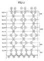
- FIGS. 1 A- FIG. 1Jare diagrams showing the fabrication processes of a semiconductor device according to a first embodiment of the present invention
- FIG. 2is a diagram showing the structure of a sample produced from the structure of FIG. 1J for measurement of a gate leakage current
- FIG. 3is a diagram showing the characteristics of the gate leakage current where a nitrogen atomic layer of FIG. 1J is not formed in the sample of FIG. 2 ;
- FIG. 4is a diagram showing the gate leakage current characteristics where the nitrogen atomic layer of FIG. 1J is formed in the sample of FIG. 2 ;
- FIGS. 5A-5Gare diagrams showing the fabrication process of a semiconductor device according to a second embodiment of the present invention.
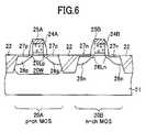
- FIG. 6is a diagram showing the structure of a CMOS semiconductor device according to a third embodiment of the present invention.
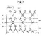
- FIGS. 1A through 1Jshow the fabricating process of a high-K dielectric gate insulation film on a Si substrate 1 of the first embodiment of the present invention.
- the high-K dielectric gate insulation filmis formed by an atomic layer depositing method in the following explanation, the high-K dielectric gate insulation film can also be formed, for example, by an MBE method and the like.
- H 2 Osteam
- H 2 O moleculesare adsorbed to the surface of the Si substrate 1 in the process of FIG. 1 B.
- the surface of the Si substrate 1is uniformly covered by a single atom thick oxygen atomic layer OL 1 .
- a bond of each oxygen atom in the oxygen atomic layer OL 1is bonded with a Si atom of the Si substrate, and the other bond of the oxygen atom is bonded with a hydrogen atom.
- a SiO 2 layer 2is formed on the surface of the Si substrate 1 in thickness of one molecule, and the surface of the SiO 2 molecule layer 2 is covered by OH basis.
- the oxygen atomic layer OL 1may not be one atom thick strictly, 90% or more of oxygen atoms are bonded with corresponding Si atoms on the Si substrate surface, which can be substantially considered that it is a single atom thick layer.
- SiCl 4 gasis supplied to the surface of the structure of FIG. 1B at the substrate temperature of 400 degrees C., and SiCl 4 molecules are adsorbed.
- hydrogen atoms in the OH basis on the surface of the oxygen atomic layer OL 1react with the SiCl 4 molecules, and are removed in the form of HCl, consequently the surface of the Si substrate is uniformly covered by the Si atomic layer SL 1 in single atom thickness.
- Two bonds of a Si atom in the Si atomic layer SL 1 produced in this mannerare bonded with two oxygen atoms in the oxygen atomic layer O 1 , and other two bonds of the Si atom are bonded with two Cl atoms.
- the Si atomic layer SL 1may not be in single atom thickness strictly, 90% or more of Si atoms are bonded with corresponding oxygen atoms of the oxygen atomic layer OL 1 , which can be substantially regarded as a single atom thick layer.
- NH 3 gasis supplied to the surface of the structure of FIG. 1C at the substrate temperature of 400 degrees C.
- a nitrogen atomic layer NL 1 in single atom thicknessis formed by replacing the Cl atoms of each Si atom in the Si atomic layer with nitrogen atoms.
- the Cl atoms previously bonded with the Si atoms in the Si atomic layer SL 1are removed in the form of HCl.
- Each of the nitrogen atoms formed in this manneris bonded with hydrogen atoms with two bonds that are not bonded with Si atoms.
- a one molecule thick SiN layer 3is formed on the one molecule thick SiO 2 molecule layer 2 .
- the nitrogen atomic layer NL 1may not be in the thickness of one atom strictly, 90% or more of the nitrogen atoms are bonded with corresponding Si atoms in the Si atomic layer SL 1 , which can be regarded substantially a single atom thick layer.
- SiCl 4 gasis supplied to the surface of the structure of FIG. 1D at the substrate temperature of 400 degrees C., and SiCl 4 molecules are adsorbed uniformly.
- the hydrogen atoms bonded with the nitrogen atoms in the nitrogen atomic layer NL 1are removed in the form of HCl. Consequently, the surface of the nitrogen atomic layer NL 1 is uniformly covered by a Si atomic layer SL 2 in single atom thickness.
- a Si atomic layer SL 2in single atom thickness.
- each of two bonds of a Si atom in the formed Si atomic layer SL 2is bonded with a nitrogen atom in the nitrogen atomic layer.
- Each of the remaining two bonds of the Si atom in the SiN molecule layerare bonded with a Cl atom.
- the Si atomic layer SL 2may not be in single atom thickness strictly, 90% or more of Si atoms are bonded with corresponding nitrogen atoms in the nitrogen atomic layer NL 1 , which can be substantially regarded as a single
- steamH 2 O
- Cl atoms that were bonded with Si atoms in the Si atomic layer SL 2are removed in the form of HCl, and an oxygen atomic layer OL 2 is formed, wherein oxygen atoms are bonded with Si atoms in the Si atomic layer SL 2 .
- the oxygen atoms in the oxygen atomic layer OL 2 and the Si atoms in the Si atomic layer SL 2may be considered as constituting a SiO 2 monomolecular layer, also they can be regarded as constituting a part of a high-K dielectric film as explained below.
- Each hydrogen atomis bonded with an oxygen atom in the oxygen atomic layer OL 2 , forming an OH base.
- the oxygen atomic layer OL 2may not be in single atom thickness strictly, 90% or more of oxygen atoms are bonded with Si atoms in the Si atomic layer SL 2 , which can be substantially regarded as a single atom thick layer.
- HfCl 4 gasis supplied to the surface of the structure of FIG. 1F , and HfCl 4 molecules are uniformly adsorbed on the oxygen atomic layer OL 2 .
- the hydrogen atom that forms the OH base on the surface of the oxygen mono-atomic layer OL 2reacts with an HfCl 4 molecule, and is removed in the form of HCl. Consequently, the oxygen atomic layer OL 2 is uniformly covered by a Hf atomic layer HL 1 in single atom thickness.
- Hf atomic layer HL 1Two bonds of a Hf atom of the formed Hf atomic layer HL 1 are bonded with two oxygen atoms in the oxygen atomic layer OL 2 , and each of two other bonds is bonded with a Cl atom.
- the Hf atomic layer HL 1may not be in single atom thickness strictly, either, 90% or more of the Hf atoms in the Hf atomic layer HL 1 are bonded with corresponding oxygen atoms of the oxygen atomic layer OL 2 , which can be considered substantially that the Hf atomic layer HL 1 is in single atom thickness.
- a hydrogen atomis bonded with each of the oxygen atoms in the oxygen atomic layer OL 3 , and an OH base is formed. Also in the oxygen atomic layer OL 3 , 90% or more of oxygen atoms are bonded with corresponding Hf atoms of the Hf atomic layer HL 1 , which can be substantially regarded as constituting a single atom thick layer.
- FIG. 1 G and FIG. 1Hmay be repeated an arbitrary number of times at the process of FIG. 1I , thereby a HfO 2 layer 4 , consisting of an oxygen atomic layer OL 3 and a Hf atomic layer HL 2 , is formed on the HfO 2 monomolecular layer, and an oxygen atomic layer OL 4 is further formed on the Hf atomic layer HL 2 .
- the oxygen atomic layer OL 3 and the Hf atomic layer HL 2may not be in single atom thickness strictly, either, they can be substantially regarded as single atom thick layers.
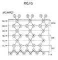
- SiCl 4 gas and NH 3 gasare supplied one by one to the structure of FIG. 1I , and a SiN monomolecular layer 5 , consisting of a Si atomic layer SL 3 and a nitrogen atomic layer NL 2 , is formed on the oxygen atomic layer OL 4 .
- a SiN monomolecular layer 5consisting of a Si atomic layer SL 3 and a nitrogen atomic layer NL 2 , is formed on the oxygen atomic layer OL 4 .
- the Si atomic layer SL 3 and the nitrogen atomic layer NL 2may not be strictly single atom thick layers, they can be substantially regarded as single atom thick layers like the previous atomic layers OL 1 through OL 4 .
- FIG. 1 A through FIG. 1Jare performed such that a thickness measured from the atomic layer OL 1 to the atomic layer NL 2 one to several nanometers, and a high-K dielectric gate insulation film is produced, on which gate electrodes, such as of poly silicon, are formed.
- the SiN monomolecular layer 3is formed on the SiO 2 monomolecular layer 2 in the process of FIG. 1D , when the HfO 2 layer is formed on this SiN layer 3 in the processes of FIG. 1 G through FIG. 1I , spreading into the Si substrate of Hf and oxygen of the HfO 2 layer is effectively suppressed. Further, with this structure, since the N atomic layer of the SiN monomolecular layer is separated from the surface of the Si substrate by the oxygen atomic layer OL 1 and the Si atomic layer SL 1 , a fluctuation of threshold characteristics of the semiconductor device due to a fixed charge of the N atom is avoided.
- the SiN molecule layer containing the nitrogen atomic layer NL 2is formed on the HfO 2 layer, thereby spread of Hf and oxygen from the HfO 2 layer to the poly silicon gate electrode is suppressed effectively. Further, dopant spread of B and the like from the poly silicon gate electrode to the Si substrate is also suppressed effectively.
- the high-K dielectric gate insulation filmhaving the structure as shown in FIG. 1J , it is important that the high-K dielectric film consisting of a laminating of HfO 2 layers is sandwiched by the oxygen atomic layers OL 2 and OL 4 . Thereby, each Hf atom is bonded with four oxygen atoms, steadily holding the Hf atom in a tetravalent state, and avoiding generation of an oxygen deficit by reduction and the like.
- one oxygen atomic layer OL 1 and one Si atomic layer SL 1are provided.
- a plurality of oxygen atomic layers and a plurality of Si atomic layersmay be provided.
- a plurality of nitrogen atomic layers NL 1 and Si atomic layers SL 2may be provided.
- thickness of the SiO 2 layerwhich is of a low dielectric constant, increases under the HfO 2 , the effect of using HfO 2 that is of a high-K dielectric constant will decrease. Therefore, there is a limit in increasing film thickness of the SiO 2 .
- ZrO 2As an alternative material for the high-K dielectric film, ZrO 2 may be considered. However, ZrO 2 tends to produce martensite type phase transition in the temperature range used in the semiconductor process. For this reason, it is more desirable to use HfO 2 that generates a phase transition at a higher temperature.
- the alternative material for the high-K dielectric filmincludes oxide and silicate of Sr, Ba, Ta, Ti, Y, Lr, and metallic elements of lanthanoid.
- FIG. 2shows a structure of a sample, wherein a poly silicon layer 6 is arranged as an electrode on the high-K dielectric gate insulation film that is formed in the manner described above.
- FIG. 3 and FIG. 4show measurement results of the leakage current characteristics of the sample shown in FIG. 2 .
- the result shown in FIG. 3represents the case where the nitrogen atomic layers NL 1 and NL 2 in FIG. 1J are omitted.
- the nitrogen atomic layers NL 1 and NL 2are formed by heat process of NH 3 gas at 650 degrees C. in the process of FIG. 1 D and FIG. 1J , respectively, and the oxygen atomic layer and the nitrogen atomic layer are formed such that a total thickness becomes about 1 nm.
- the HfO 2 layerhas a 3 nm film thickness on the whole.
- the leakage current density Jgranged between 0.43 and 55 Acm ⁇ 2 at an applied voltage of +1V.
- the leakage current density Jgranted between 0.84 and 7.88 ⁇ 10 ⁇ 5 Acm ⁇ 2 at the applied voltage of +1V, which is a significant reduction in comparison with the case of FIG. 10 .
- the film thicknessranged between 1.77 and 1.84 nm in terms of oxide equivalent thickness.
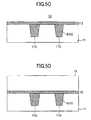
- FIGS. 5A through 5Gshow a manufacturing process of the semiconductor device 10 of a second embodiment of the present invention.
- a thermal oxidation layer 11 ais formed by a thermal oxidation processing, and a SiN film 11 b is further formed by CVD on the thermal oxidation film 11 a.
- openings corresponding to isolation areasare formed by dry etching patterning of the SiN film 11 b , and further openings that expose the Si substrate 11 are formed by dry etching patterning applied to the thermal oxidation film 11 a , using the SiN film 11 b as a mask. Further, isolation slots 11 A and 11 B having an inclined sidewall are formed corresponding to the openings are formed by wet etching the exposed Si substrate 11 , using the SiN film 11 b as a mask.
- thermal oxidationis applied to the structure of FIG. 5A , and a liner oxide film that is omitted in the figure is formed on the sidewall and the bottom of the isolation slots 11 A and 11 B.
- the isolation slots 11 A and 11 Bare filled with a CVD-SiO 2 film.
- the CVD-SiO 2 film, the SiN film 11 b under it, and the thermal oxidation film 11 a under itare ground and removed by the CMP method, and the SiO 2 isolation regions 11 C and 11 D that fill the isolation slots 11 A and 11 B are formed.
- the surface of the Si substrate 11is exposed, which is sacrifice-oxidized. Then, the sacrifice-oxidized surface is removed by an HF processing, such that a fresh Si substrate surface is exposed.
- a poly silicon layer 13is deposited on the gate insulation film 12 , resulting in the same structure as FIG. 2 .
- the poly silicon film 13 and the gate insulation film 12are patterned, and poly silicon gate electrodes 13 A, 13 B, and 13 C are formed.
- n-type impuritiesare implanted, using the poly silicon gate electrodes 13 A through 13 C as a mask.
- LDD spread areasare formed inside the Si substrate 11 .
- an LDD spread area 14 Ais formed on the both sides of the gate electrode 13 A
- an LDD spread area 14 Bis formed on the both sides of the gate electrode 13 B
- an LDD spread area 14 Cis further formed on the both sides of the gate electrode 13 C.
- a sidewall insulation filmis formed on the sidewall of each of the gate electrodes 13 A, 13 B, and 13 C. Ion implantation is performed, using the gate electrodes 13 A, 13 B and 13 C and the sidewall film as a mask, thereby spread areas 15 A, 15 B, and 15 C are formed outside each of the LDD spread areas 14 A, 14 B, and 14 C.
- low resistance silicide layers 13 a through 13 c and 15 a through 15 c of such as CoSi 2are formed on the surface of the gate electrodes 13 A through 13 C and the spread areas 15 A through 15 C, respectively, by a salicide process.
- a SiN film 16is formed by CVD on the structure of FIG. 5F such that the gate electrodes 13 A through 13 C are covered, and a layer insulation film 17 is further formed on the SiN film 16 .
- the layer insulation film 17is made flat by the CMF method, contact holes that expose the spread areas 15 A through 15 C are formed, and contact plugs 18 A through 18 C are formed in the contact holes such that the spread areas 15 A through 15 C, respectively, are contacted.
- the semiconductor device of the present inventionincludes a high-K dielectric gate insulation film as the gate insulation film 12 formed by the process of FIG. 5C , realizing short gate length of 0.1 micrometers or less. Physical film thickness of the gate insulation film of 1 through several nm is attained, suppressing the gate leakage current by the direct tunnel effect.
- the semiconductor device of the present inventionincludes an oxygen atomic layer in the portion where the gate insulation film 12 directly touches the Si substrate 11 that constitutes a channel region, stable threshold characteristics are attained without forming a dangling bond and an interface level in the interface between the substrate and the gate insulation film.
- the semiconductor device of the present inventionsince the high-K dielectric film is sandwiched by the nitrogen atomic layers, metallic elements and oxygen in the high-K dielectric film are not spread into the Si substrate 11 or the poly silicon gate electrodes 13 A through 13 C, resulting in excellent threshold characteristics. Further, spread of the dopant impurities to the Si substrate through the gate insulation film 12 from the poly silicon gate electrode is also suppressed, and a fluctuation of the threshold characteristics is suppressed.
- the nitrogen atomic layeris formed separately from the Si substrate surface by the oxygen atomic layer and the Si atomic layer, a fluctuation of the threshold characteristics due to the fixed charge of a nitrogen atom can be suppressed.
- the high-K dielectric layeris sandwiched by the oxygen atomic layers, the valence of metallic elements, such as Zr and Hf in the high-K dielectrics layer, is stabilized, and a problem, such as decline in the relative dielectric constant, can be avoided.
- FIG. 6shows a structure of a CMOS semiconductor device 20 of a third embodiment of the present invention.
- the CMOS semiconductor device 20includes an isolation area 22 that divides a p-type Si substrate 21 into a p-channel MOS area 20 A and an n-channel MOS area 20 B. In the p-channel MOS area 20 A, an n-type well 20 W is formed.
- a high-K dielectric gate insulation film 23 Athat has the same layer structure as shown in FIG. 1J is formed, corresponding to the channel region, and a poly silicon gate electrode 24 A doped by B is formed on the gate insulation film 23 A. Further, on the poly silicon gate electrode 24 A, a silicide layer 25 A is formed by the salicide process. Further, a sidewall film is formed on the both sides of the poly silicon gate electrode 24 A.
- a p-type LDO area 26 Lpis formed corresponding to each side of the surface of the wall of the gate electrode 24 A by ion implantation of B into the well 20 W, and a p+ type spread area 26 p is further formed outside the side wall insulation film. Further, a silicide low resistance layer 27 p is formed on the surface of the p+ type spread area.
- a high-K dielectric gate insulation film 23 Bthat has the same layer structure as shown in FIG. 1J is formed, corresponding to the channel region, and a poly silicon gate electrode 24 B doped by As or P is formed on the gate insulation film 23 B. Further, on the poly silicon gate electrode 24 B, a silicide layer 25 B is formed by the salicide process. Further, a sidewall film is formed on the both sides of the poly silicon-gate electrode 25 B.
- an n-type LDD area 26 Lnis formed by ion implantation of As or P, and an n+ type spread area 26 n is further formed outside the sidewall insulation film. Further, a silicide low resistance layer 27 n is formed on the surface of the n+ type spread area 26 n.
- each of the p-channel MOS transistor and n-channel MOS transistoris formed with very short gate length of 0.1 micrometers or less. Therefore, when decreasing oxide equivalent film thickness of a gate insulation film, the gate insulation films 23 A and 23 B can be formed in 1 through several nm of physical film thickness, and an increase of the gate leakage current by the tunnel current can be avoided.
- the nitrogen atomic layers NL 1 and NL 2are formed in the film, spread of oxygen and metallic elements, such as Hf and Zr, through the gate insulation film 23 A and 23 B is suppressed effectively. Further, since a high-quality SiO 2 molecule layer is formed in the portion that touches the Si channel region, formation of a dangling bond in the interface between the Si substrate and the gate insulation film, and an interface level are avoided, and stable threshold characteristics are attained. Further, since the nitrogen atomic layer NL 1 is formed separately from the Si substrate surface, a fluctuation of the threshold characteristics by the fixed charge of a nitrogen atom is also avoided.
- the spread of B from poly silicon gate electrode 24 A to the Si substrate 21is suppressed by formation of the nitrogen atomic layers NL 1 and NL 2 , and doping of the channel region that brings about a fluctuation of the threshold characteristics is avoided.
Landscapes
- Chemical & Material Sciences (AREA)
- Engineering & Computer Science (AREA)
- Power Engineering (AREA)
- Physics & Mathematics (AREA)
- Microelectronics & Electronic Packaging (AREA)
- Computer Hardware Design (AREA)
- Manufacturing & Machinery (AREA)
- General Physics & Mathematics (AREA)
- Condensed Matter Physics & Semiconductors (AREA)
- General Chemical & Material Sciences (AREA)
- Chemical Kinetics & Catalysis (AREA)
- Organic Chemistry (AREA)
- Metallurgy (AREA)
- Mechanical Engineering (AREA)
- Materials Engineering (AREA)
- Inorganic Chemistry (AREA)
- Crystallography & Structural Chemistry (AREA)
- Insulated Gate Type Field-Effect Transistor (AREA)
- Metal-Oxide And Bipolar Metal-Oxide Semiconductor Integrated Circuits (AREA)
- Formation Of Insulating Films (AREA)
Abstract
Description
- a channel area formed in a Si crystal layer,
- a gate insulation film formed on the channel area, containing a SiO layer that is formed on the Si crystal layer, a first SiN layer formed on the SiO layer, a dielectric metal oxide layer formed on the first SiN layer, and a second SiN layer formed on the dielectric metal oxide layer, and
- a gate electrode formed on the gate insulation film.
- a Si substrate,
- a gate insulation film formed on the Si substrate, and
- a gate electrode formed on the gate insulation film; wherein the gate insulation film, comprising:
- a first insulation film that comprises an oxygen atomic layer consisting of oxygen atoms, each of which is bonded with a Si atom of surface of the Si substrate, a first Si atomic layer consisting of Si atoms, each of which is bonded with an oxygen atom in the oxygen atomic layer, a nitrogen atomic layer consisting of nitrogen atoms, each of which is bonded with a Si atom in the Si atomic layer, and a second Si atomic layer, consisting of Si atoms, each of which is bonded with a nitrogen atom in the nitrogen atomic layer,
- a second insulation film that comprises an oxygen atomic layer consisting of oxygen atoms, each of which is bonded with a Si atom in the second Si atomic layer, a metal atomic layer consisting of metal atoms, each of which is bonded with an oxygen atom in the oxygen atomic layer, an oxygen atomic layer consisting of oxygen atoms, each of which is bonded with a metal atom in the metal atomic layer, and, at the topmost part, a topmost oxygen atomic layer consisting of oxygen atoms, each of which is bonded with a metal atom in the metal atomic layer, and
- a third insulation film that comprises a Si atomic layer that covers the topmost oxygen atomic layer, consisting of Si atoms, each of which is bonded with an oxygen atom in the topmost oxygen atomic layer, and a nitrogen atomic layer, consisting of nitrogen atoms, each of which is bonded with a Si atom in the Si atomic layer that covers the topmost oxygen atomic layer.
- (A) a process wherein gas-phase Si is supplied to Si substrate surface, such that the Si substrate surface adsorbs Si molecules in single molecule thickness,
- (B) a process wherein a gas containing oxygen is supplied to the Si substrate surface that adsorbed the Si molecules after the process (A), such that the adsorbed Si molecules are oxidized, producing a SiO molecule layer on the Si substrate surface,
- (C) a process wherein gas-phase Si is supplied to the Si substrate surface which is covered by the SiO molecule layer after the process (B), such that Si molecules are adsorbed in single molecule thickness,
- (D) a process wherein a gas containing nitrogen is supplied to the Si substrate surface that adsorbs the Si molecules after the process (C), such that the adsorbed Si molecules form a SiN molecule layer on the Si substrate surface,
- (E) a process wherein a gas containing oxygen, and a gas containing metallic elements are alternately supplied to the Si substrate surface that is covered by the SiN molecule layer after the process (D), such that a dielectrics metal oxide film is formed,
- (F) a process wherein gas-phase Si is supplied to the substrate surface which is covered by the dielectric metal oxide film after the process (E), such that Si molecules are adsorbed in single molecule thickness, forming a Si molecule layer, and
- (G) a process wherein a gas containing nitrogen is supplied to the substrate surface, which is covered by the Si molecule layer after the process (F), such that the adsorbed Si molecules form a SiN molecule layer on the Si substrate surface.
Claims (17)
Applications Claiming Priority (4)
| Application Number | Priority Date | Filing Date | Title |
|---|---|---|---|
| JP2001097128 | 2001-03-29 | ||
| JP2001-097128 | 2001-03-29 | ||
| JP2002-077055 | 2002-03-19 | ||
| JP2002077055AJP3792589B2 (en) | 2001-03-29 | 2002-03-19 | Manufacturing method of semiconductor device |
Publications (2)
| Publication Number | Publication Date |
|---|---|
| US20020146916A1 US20020146916A1 (en) | 2002-10-10 |
| US6894369B2true US6894369B2 (en) | 2005-05-17 |
Family
ID=26612622
Family Applications (1)
| Application Number | Title | Priority Date | Filing Date |
|---|---|---|---|
| US10/109,001Expired - LifetimeUS6894369B2 (en) | 2001-03-29 | 2002-03-29 | Semiconductor device having a high-dielectric gate insulation film and fabrication process thereof |
Country Status (5)
| Country | Link |
|---|---|
| US (1) | US6894369B2 (en) |
| JP (1) | JP3792589B2 (en) |
| KR (1) | KR100757645B1 (en) |
| CN (1) | CN1206736C (en) |
| TW (1) | TW544735B (en) |
Cited By (16)
| Publication number | Priority date | Publication date | Assignee | Title |
|---|---|---|---|---|
| US20060131672A1 (en)* | 2004-12-20 | 2006-06-22 | Chih-Hao Wang | Nitrogen treatment to improve high-k gate dielectrics |
| US20070017666A1 (en)* | 2005-07-19 | 2007-01-25 | Goenka Lakhi N | Energy management system for a hybrid-electric vehicle |
| KR100757645B1 (en)* | 2001-03-29 | 2007-09-10 | 후지쯔 가부시끼가이샤 | Semiconductor device and complementary semiconductor device |
| US20080203500A1 (en)* | 2003-06-20 | 2008-08-28 | Nec Corporation | Semiconductor device and production method therefor |
| US20080230618A1 (en)* | 2004-05-10 | 2008-09-25 | Bsst Llc | Climate control system for hybrid vehicles using thermoelectric devices |
| US20090042381A1 (en)* | 2007-08-07 | 2009-02-12 | Chen-Hua Yu | High-K Gate Dielectric and Method of Manufacture |
| US20100022841A1 (en)* | 2008-07-22 | 2010-01-28 | Fujifilm Corporation | Endoscope optical system device and endoscope with the same |
| US20100052374A1 (en)* | 2007-05-25 | 2010-03-04 | Bsst Llc | System and method for climate control within a passenger compartment of a vehicle |
| US20100155018A1 (en)* | 2008-12-19 | 2010-06-24 | Lakhi Nandlal Goenka | Hvac system for a hybrid vehicle |
| US20100287952A1 (en)* | 2009-05-18 | 2010-11-18 | Lakhi Nandlal Goenka | Temperature control system with thermoelectric device |
| US20100313576A1 (en)* | 2006-08-02 | 2010-12-16 | Lakhi Nandlal Goenka | Hybrid vehicle temperature control systems and methods |
| US7870745B2 (en) | 2006-03-16 | 2011-01-18 | Bsst Llc | Thermoelectric device efficiency enhancement using dynamic feedback |
| US8408012B2 (en) | 2005-04-08 | 2013-04-02 | Bsst Llc | Thermoelectric-based heating and cooling system |
| US8613200B2 (en) | 2008-10-23 | 2013-12-24 | Bsst Llc | Heater-cooler with bithermal thermoelectric device |
| US9178128B2 (en) | 2011-11-17 | 2015-11-03 | Gentherm Incorporated | Thermoelectric devices with interface materials and methods of manufacturing the same |
| US10991869B2 (en) | 2018-07-30 | 2021-04-27 | Gentherm Incorporated | Thermoelectric device having a plurality of sealing materials |
Families Citing this family (54)
| Publication number | Priority date | Publication date | Assignee | Title |
|---|---|---|---|---|
| US6852167B2 (en) | 2001-03-01 | 2005-02-08 | Micron Technology, Inc. | Methods, systems, and apparatus for uniform chemical-vapor depositions |
| JP4104834B2 (en)* | 2001-04-13 | 2008-06-18 | 株式会社東芝 | Manufacturing method of MIS field effect transistor |
| US6844203B2 (en) | 2001-08-30 | 2005-01-18 | Micron Technology, Inc. | Gate oxides, and methods of forming |
| US8026161B2 (en) | 2001-08-30 | 2011-09-27 | Micron Technology, Inc. | Highly reliable amorphous high-K gate oxide ZrO2 |
| US6960537B2 (en)* | 2001-10-02 | 2005-11-01 | Asm America, Inc. | Incorporation of nitrogen into high k dielectric film |
| US6953730B2 (en) | 2001-12-20 | 2005-10-11 | Micron Technology, Inc. | Low-temperature grown high quality ultra-thin CoTiO3 gate dielectrics |
| US6767795B2 (en) | 2002-01-17 | 2004-07-27 | Micron Technology, Inc. | Highly reliable amorphous high-k gate dielectric ZrOXNY |
| US6893984B2 (en)* | 2002-02-20 | 2005-05-17 | Micron Technology Inc. | Evaporated LaA1O3 films for gate dielectrics |
| US6812100B2 (en) | 2002-03-13 | 2004-11-02 | Micron Technology, Inc. | Evaporation of Y-Si-O films for medium-k dielectrics |
| US7160577B2 (en) | 2002-05-02 | 2007-01-09 | Micron Technology, Inc. | Methods for atomic-layer deposition of aluminum oxides in integrated circuits |
| US7589029B2 (en) | 2002-05-02 | 2009-09-15 | Micron Technology, Inc. | Atomic layer deposition and conversion |
| US7205218B2 (en) | 2002-06-05 | 2007-04-17 | Micron Technology, Inc. | Method including forming gate dielectrics having multiple lanthanide oxide layers |
| US7135421B2 (en) | 2002-06-05 | 2006-11-14 | Micron Technology, Inc. | Atomic layer-deposited hafnium aluminum oxide |
| US7221586B2 (en) | 2002-07-08 | 2007-05-22 | Micron Technology, Inc. | Memory utilizing oxide nanolaminates |
| US6921702B2 (en)* | 2002-07-30 | 2005-07-26 | Micron Technology Inc. | Atomic layer deposited nanolaminates of HfO2/ZrO2 films as gate dielectrics |
| US6967154B2 (en) | 2002-08-26 | 2005-11-22 | Micron Technology, Inc. | Enhanced atomic layer deposition |
| US7199023B2 (en)* | 2002-08-28 | 2007-04-03 | Micron Technology, Inc. | Atomic layer deposited HfSiON dielectric films wherein each precursor is independendently pulsed |
| US7084078B2 (en) | 2002-08-29 | 2006-08-01 | Micron Technology, Inc. | Atomic layer deposited lanthanide doped TiOx dielectric films |
| US6607973B1 (en)* | 2002-09-16 | 2003-08-19 | Advanced Micro Devices, Inc. | Preparation of high-k nitride silicate layers by cyclic molecular layer deposition |
| US6958302B2 (en) | 2002-12-04 | 2005-10-25 | Micron Technology, Inc. | Atomic layer deposited Zr-Sn-Ti-O films using TiI4 |
| US7101813B2 (en) | 2002-12-04 | 2006-09-05 | Micron Technology Inc. | Atomic layer deposited Zr-Sn-Ti-O films |
| JP3776889B2 (en)* | 2003-02-07 | 2006-05-17 | 株式会社東芝 | Semiconductor device and manufacturing method thereof |
| US7192892B2 (en) | 2003-03-04 | 2007-03-20 | Micron Technology, Inc. | Atomic layer deposited dielectric layers |
| JP4507232B2 (en) | 2003-03-24 | 2010-07-21 | ローム株式会社 | Manufacturing method of semiconductor device |
| US7135369B2 (en) | 2003-03-31 | 2006-11-14 | Micron Technology, Inc. | Atomic layer deposited ZrAlxOy dielectric layers including Zr4AlO9 |
| US7183186B2 (en) | 2003-04-22 | 2007-02-27 | Micro Technology, Inc. | Atomic layer deposited ZrTiO4 films |
| US7192824B2 (en) | 2003-06-24 | 2007-03-20 | Micron Technology, Inc. | Lanthanide oxide / hafnium oxide dielectric layers |
| JP2005023199A (en)* | 2003-07-02 | 2005-01-27 | Chisso Corp | Functional ultrathin film and method for forming the same |
| JP2005064317A (en)* | 2003-08-18 | 2005-03-10 | Semiconductor Leading Edge Technologies Inc | Semiconductor device |
| JP4059183B2 (en)* | 2003-10-07 | 2008-03-12 | ソニー株式会社 | Insulator thin film manufacturing method |
| US20050233477A1 (en)* | 2004-03-05 | 2005-10-20 | Tokyo Electron Limited | Substrate processing apparatus, substrate processing method, and program for implementing the method |
| JP2005277223A (en)* | 2004-03-25 | 2005-10-06 | National Institute Of Advanced Industrial & Technology | Semiconductor device and manufacturing method thereof |
| US7601649B2 (en) | 2004-08-02 | 2009-10-13 | Micron Technology, Inc. | Zirconium-doped tantalum oxide films |
| US7081421B2 (en) | 2004-08-26 | 2006-07-25 | Micron Technology, Inc. | Lanthanide oxide dielectric layer |
| US7494939B2 (en) | 2004-08-31 | 2009-02-24 | Micron Technology, Inc. | Methods for forming a lanthanum-metal oxide dielectric layer |
| US7588988B2 (en) | 2004-08-31 | 2009-09-15 | Micron Technology, Inc. | Method of forming apparatus having oxide films formed using atomic layer deposition |
| US7235501B2 (en) | 2004-12-13 | 2007-06-26 | Micron Technology, Inc. | Lanthanum hafnium oxide dielectrics |
| US7560395B2 (en) | 2005-01-05 | 2009-07-14 | Micron Technology, Inc. | Atomic layer deposited hafnium tantalum oxide dielectrics |
| JP4185057B2 (en) | 2005-01-28 | 2008-11-19 | 富士通株式会社 | Manufacturing method of semiconductor device |
| US7508648B2 (en)* | 2005-02-08 | 2009-03-24 | Micron Technology, Inc. | Atomic layer deposition of Dy doped HfO2 films as gate dielectrics |
| US7374964B2 (en) | 2005-02-10 | 2008-05-20 | Micron Technology, Inc. | Atomic layer deposition of CeO2/Al2O3 films as gate dielectrics |
| US7399666B2 (en) | 2005-02-15 | 2008-07-15 | Micron Technology, Inc. | Atomic layer deposition of Zr3N4/ZrO2 films as gate dielectrics |
| US7498247B2 (en) | 2005-02-23 | 2009-03-03 | Micron Technology, Inc. | Atomic layer deposition of Hf3N4/HfO2 films as gate dielectrics |
| US7687409B2 (en) | 2005-03-29 | 2010-03-30 | Micron Technology, Inc. | Atomic layer deposited titanium silicon oxide films |
| US7390756B2 (en) | 2005-04-28 | 2008-06-24 | Micron Technology, Inc. | Atomic layer deposited zirconium silicon oxide films |
| US7662729B2 (en) | 2005-04-28 | 2010-02-16 | Micron Technology, Inc. | Atomic layer deposition of a ruthenium layer to a lanthanide oxide dielectric layer |
| US7927948B2 (en) | 2005-07-20 | 2011-04-19 | Micron Technology, Inc. | Devices with nanocrystals and methods of formation |
| US7473637B2 (en) | 2005-07-20 | 2009-01-06 | Micron Technology, Inc. | ALD formed titanium nitride films |
| US8110469B2 (en) | 2005-08-30 | 2012-02-07 | Micron Technology, Inc. | Graded dielectric layers |
| US7709402B2 (en) | 2006-02-16 | 2010-05-04 | Micron Technology, Inc. | Conductive layers for hafnium silicon oxynitride films |
| US7563730B2 (en) | 2006-08-31 | 2009-07-21 | Micron Technology, Inc. | Hafnium lanthanide oxynitride films |
| US7605030B2 (en) | 2006-08-31 | 2009-10-20 | Micron Technology, Inc. | Hafnium tantalum oxynitride high-k dielectric and metal gates |
| US7759237B2 (en) | 2007-06-28 | 2010-07-20 | Micron Technology, Inc. | Method of forming lutetium and lanthanum dielectric structures |
| CN102077331B (en)* | 2008-06-27 | 2014-05-07 | 株式会社半导体能源研究所 | Thin film transistor |
Citations (7)
| Publication number | Priority date | Publication date | Assignee | Title |
|---|---|---|---|---|
| EP1124262A2 (en) | 2000-02-11 | 2001-08-16 | Sharp Kabushiki Kaisha | Multilayer dielectric stack and method |
| US20010029068A1 (en)* | 1999-02-26 | 2001-10-11 | Sailesh Chittipeddi | Semiconductor device structure including a tantalum pentoxide layer sandwiched between silicon nitride layers |
| US20020137339A1 (en)* | 1996-03-26 | 2002-09-26 | Hideki Takeuchi | Semiconductor device and manufacturing method thereof |
| US6602753B2 (en)* | 2000-07-26 | 2003-08-05 | Kabushiki Kaisha Toshiba | Semiconductor device having a gate insulating film comprising a metal oxide and method of manufacturing the same |
| US20040072383A1 (en)* | 2002-07-08 | 2004-04-15 | Nichia Corporation | Nitride semiconductor device comprising bonded substrate and fabrication method of the same |
| US6770974B2 (en)* | 2000-06-30 | 2004-08-03 | Sony Corporation | Semiconductor device and its manufacturing method |
| US20040152340A1 (en)* | 1999-06-04 | 2004-08-05 | Naoki Yamamoto | Semiconductor integrated circuit device and method for manufacturing the same |
Family Cites Families (4)
| Publication number | Priority date | Publication date | Assignee | Title |
|---|---|---|---|---|
| KR100567299B1 (en)* | 1998-03-27 | 2006-04-04 | 텍사스 인스트루먼츠 인코포레이티드 | Semiconductor device and method for manufacturing gate structure of semiconductor device |
| JP3513018B2 (en)* | 1998-06-30 | 2004-03-31 | 株式会社東芝 | Semiconductor device and manufacturing method thereof |
| KR100297719B1 (en)* | 1998-10-16 | 2001-08-07 | 윤종용 | Method for manufacturing thin film |
| JP3792589B2 (en)* | 2001-03-29 | 2006-07-05 | 富士通株式会社 | Manufacturing method of semiconductor device |
- 2002
- 2002-03-19JPJP2002077055Apatent/JP3792589B2/ennot_activeExpired - Lifetime
- 2002-03-27KRKR1020020016641Apatent/KR100757645B1/ennot_activeExpired - Fee Related
- 2002-03-28TWTW091106211Apatent/TW544735B/ennot_activeIP Right Cessation
- 2002-03-29USUS10/109,001patent/US6894369B2/ennot_activeExpired - Lifetime
- 2002-03-29CNCNB021218447Apatent/CN1206736C/ennot_activeExpired - Lifetime
Patent Citations (9)
| Publication number | Priority date | Publication date | Assignee | Title |
|---|---|---|---|---|
| US20020137339A1 (en)* | 1996-03-26 | 2002-09-26 | Hideki Takeuchi | Semiconductor device and manufacturing method thereof |
| US20010029068A1 (en)* | 1999-02-26 | 2001-10-11 | Sailesh Chittipeddi | Semiconductor device structure including a tantalum pentoxide layer sandwiched between silicon nitride layers |
| US6482694B2 (en)* | 1999-02-26 | 2002-11-19 | Agere Systems, Inc. | Semiconductor device structure including a tantalum pentoxide layer sandwiched between silicon nitride layers |
| US20040152340A1 (en)* | 1999-06-04 | 2004-08-05 | Naoki Yamamoto | Semiconductor integrated circuit device and method for manufacturing the same |
| EP1124262A2 (en) | 2000-02-11 | 2001-08-16 | Sharp Kabushiki Kaisha | Multilayer dielectric stack and method |
| JP2001267566A (en) | 2000-02-11 | 2001-09-28 | Sharp Corp | Multilayer dielectric stack and method |
| US6770974B2 (en)* | 2000-06-30 | 2004-08-03 | Sony Corporation | Semiconductor device and its manufacturing method |
| US6602753B2 (en)* | 2000-07-26 | 2003-08-05 | Kabushiki Kaisha Toshiba | Semiconductor device having a gate insulating film comprising a metal oxide and method of manufacturing the same |
| US20040072383A1 (en)* | 2002-07-08 | 2004-04-15 | Nichia Corporation | Nitride semiconductor device comprising bonded substrate and fabrication method of the same |
Cited By (37)
| Publication number | Priority date | Publication date | Assignee | Title |
|---|---|---|---|---|
| KR100757645B1 (en)* | 2001-03-29 | 2007-09-10 | 후지쯔 가부시끼가이샤 | Semiconductor device and complementary semiconductor device |
| US20080203500A1 (en)* | 2003-06-20 | 2008-08-28 | Nec Corporation | Semiconductor device and production method therefor |
| US7870892B2 (en) | 2004-05-10 | 2011-01-18 | Bsst Llc | Climate control method for hybrid vehicles using thermoelectric devices |
| US20080230618A1 (en)* | 2004-05-10 | 2008-09-25 | Bsst Llc | Climate control system for hybrid vehicles using thermoelectric devices |
| US7564108B2 (en)* | 2004-12-20 | 2009-07-21 | Taiwan Semiconductor Manufacturing Company, Ltd. | Nitrogen treatment to improve high-k gate dielectrics |
| US20060131672A1 (en)* | 2004-12-20 | 2006-06-22 | Chih-Hao Wang | Nitrogen treatment to improve high-k gate dielectrics |
| US8915091B2 (en) | 2005-04-08 | 2014-12-23 | Gentherm Incorporated | Thermoelectric-based thermal management system |
| US9863672B2 (en) | 2005-04-08 | 2018-01-09 | Gentherm Incorporated | Thermoelectric-based air conditioning system |
| US8408012B2 (en) | 2005-04-08 | 2013-04-02 | Bsst Llc | Thermoelectric-based heating and cooling system |
| US20070017666A1 (en)* | 2005-07-19 | 2007-01-25 | Goenka Lakhi N | Energy management system for a hybrid-electric vehicle |
| US8783397B2 (en) | 2005-07-19 | 2014-07-22 | Bsst Llc | Energy management system for a hybrid-electric vehicle |
| US8261868B2 (en) | 2005-07-19 | 2012-09-11 | Bsst Llc | Energy management system for a hybrid-electric vehicle |
| US7870745B2 (en) | 2006-03-16 | 2011-01-18 | Bsst Llc | Thermoelectric device efficiency enhancement using dynamic feedback |
| US20110107772A1 (en)* | 2006-03-16 | 2011-05-12 | Lakhi Nandlal Goenka | Thermoelectric device efficiency enhancement using dynamic feedback |
| US8424315B2 (en) | 2006-03-16 | 2013-04-23 | Bsst Llc | Thermoelectric device efficiency enhancement using dynamic feedback |
| US9103573B2 (en) | 2006-08-02 | 2015-08-11 | Gentherm Incorporated | HVAC system for a vehicle |
| US20100313576A1 (en)* | 2006-08-02 | 2010-12-16 | Lakhi Nandlal Goenka | Hybrid vehicle temperature control systems and methods |
| US8631659B2 (en) | 2006-08-02 | 2014-01-21 | Bsst Llc | Hybrid vehicle temperature control systems and methods |
| US9310112B2 (en) | 2007-05-25 | 2016-04-12 | Gentherm Incorporated | System and method for distributed thermoelectric heating and cooling |
| US10464391B2 (en) | 2007-05-25 | 2019-11-05 | Gentherm Incorporated | System and method for distributed thermoelectric heating and cooling |
| US20100052374A1 (en)* | 2007-05-25 | 2010-03-04 | Bsst Llc | System and method for climate control within a passenger compartment of a vehicle |
| US9366461B2 (en) | 2007-05-25 | 2016-06-14 | Gentherm Incorporated | System and method for climate control within a passenger compartment of a vehicle |
| US7998820B2 (en) | 2007-08-07 | 2011-08-16 | Taiwan Semiconductor Manufacturing Company, Ltd. | High-k gate dielectric and method of manufacture |
| US8294201B2 (en) | 2007-08-07 | 2012-10-23 | Taiwan Semiconductor Manufacturing Company, Ltd. | High-k gate dielectric and method of manufacture |
| US20090042381A1 (en)* | 2007-08-07 | 2009-02-12 | Chen-Hua Yu | High-K Gate Dielectric and Method of Manufacture |
| US20100022841A1 (en)* | 2008-07-22 | 2010-01-28 | Fujifilm Corporation | Endoscope optical system device and endoscope with the same |
| US8613200B2 (en) | 2008-10-23 | 2013-12-24 | Bsst Llc | Heater-cooler with bithermal thermoelectric device |
| US20100155018A1 (en)* | 2008-12-19 | 2010-06-24 | Lakhi Nandlal Goenka | Hvac system for a hybrid vehicle |
| US9038400B2 (en) | 2009-05-18 | 2015-05-26 | Gentherm Incorporated | Temperature control system with thermoelectric device |
| US10106011B2 (en) | 2009-05-18 | 2018-10-23 | Gentherm Incorporated | Temperature control system with thermoelectric device |
| US20100287952A1 (en)* | 2009-05-18 | 2010-11-18 | Lakhi Nandlal Goenka | Temperature control system with thermoelectric device |
| US11203249B2 (en) | 2009-05-18 | 2021-12-21 | Gentherm Incorporated | Temperature control system with thermoelectric device |
| US9178128B2 (en) | 2011-11-17 | 2015-11-03 | Gentherm Incorporated | Thermoelectric devices with interface materials and methods of manufacturing the same |
| US9865794B2 (en) | 2011-11-17 | 2018-01-09 | Gentherm Incorporated | Thermoelectric devices with interface materials and methods of manufacturing the same |
| US10991869B2 (en) | 2018-07-30 | 2021-04-27 | Gentherm Incorporated | Thermoelectric device having a plurality of sealing materials |
| US11075331B2 (en) | 2018-07-30 | 2021-07-27 | Gentherm Incorporated | Thermoelectric device having circuitry with structural rigidity |
| US11223004B2 (en) | 2018-07-30 | 2022-01-11 | Gentherm Incorporated | Thermoelectric device having a polymeric coating |
Also Published As
| Publication number | Publication date |
|---|---|
| CN1206736C (en) | 2005-06-15 |
| TW544735B (en) | 2003-08-01 |
| JP3792589B2 (en) | 2006-07-05 |
| KR100757645B1 (en) | 2007-09-10 |
| KR20020077126A (en) | 2002-10-11 |
| US20020146916A1 (en) | 2002-10-10 |
| JP2002359370A (en) | 2002-12-13 |
| CN1384549A (en) | 2002-12-11 |
Similar Documents
| Publication | Publication Date | Title |
|---|---|---|
| US6894369B2 (en) | Semiconductor device having a high-dielectric gate insulation film and fabrication process thereof | |
| US5436481A (en) | MOS-type semiconductor device and method of making the same | |
| US7514753B2 (en) | Semiconductor device | |
| US7687869B2 (en) | Semiconductor device and method of manufacturing the same | |
| US20050070123A1 (en) | Method for forming a thin film and method for fabricating a semiconductor device | |
| US20080164536A1 (en) | Transistors and Methods of Manufacture Thereof | |
| US20070278587A1 (en) | Semiconductor device and manufacturing method thereof | |
| JP4860183B2 (en) | Semiconductor device and manufacturing method thereof | |
| US20120299113A1 (en) | Semiconductor device and method for fabricating the same | |
| JP2005079223A (en) | Semiconductor device and manufacturing method of semiconductor device | |
| US7834408B2 (en) | Semiconductor device and method for manufacturing the same | |
| JP2006344836A (en) | Semiconductor device and manufacturing method thereof | |
| JP2002359371A (en) | Semiconductor device and manufacturing method thereof | |
| JP2011003717A (en) | Semiconductor apparatus and method of manufacturing the same | |
| US7238996B2 (en) | Semiconductor device | |
| JP2011253931A (en) | Semiconductor device and method of manufacturing the same | |
| US20050253181A1 (en) | Semiconductor device | |
| US20080023765A1 (en) | Semiconductor Devices and Methods of Fabricating the Same | |
| JP2010123669A (en) | Semiconductor device and manufacturing method thereof | |
| KR100655658B1 (en) | Gate electrode structure and manufacturing method thereof, semiconductor transistor having same and manufacturing method thereof | |
| JP3779556B2 (en) | Field effect transistor | |
| JP2006269520A (en) | Semiconductor device and manufacturing method thereof | |
| JP2004221309A (en) | Semiconductor device and manufacturing method thereof | |
| JP2006319091A (en) | Manufacturing method of semiconductor device | |
| JP2008130798A (en) | Semiconductor device and manufacturing method thereof |
Legal Events
| Date | Code | Title | Description |
|---|---|---|---|
| AS | Assignment | Owner name:FUJITSU LIMITED, JAPAN Free format text:ASSIGNMENT OF ASSIGNORS INTEREST;ASSIGNORS:IRINO, KIYOSHI;MORISAKI, YUSUKE;SUGITA, YOSHIHIRO;AND OTHERS;REEL/FRAME:012994/0968 Effective date:20020531 | |
| STCF | Information on status: patent grant | Free format text:PATENTED CASE | |
| FEPP | Fee payment procedure | Free format text:PAYOR NUMBER ASSIGNED (ORIGINAL EVENT CODE: ASPN); ENTITY STATUS OF PATENT OWNER: LARGE ENTITY | |
| FPAY | Fee payment | Year of fee payment:4 | |
| AS | Assignment | Owner name:FUJITSU MICROELECTRONICS LIMITED, JAPAN Free format text:ASSIGNMENT OF ASSIGNORS INTEREST;ASSIGNOR:FUJITSU LIMITED;REEL/FRAME:021976/0089 Effective date:20081104 Owner name:FUJITSU MICROELECTRONICS LIMITED,JAPAN Free format text:ASSIGNMENT OF ASSIGNORS INTEREST;ASSIGNOR:FUJITSU LIMITED;REEL/FRAME:021976/0089 Effective date:20081104 | |
| AS | Assignment | Owner name:FUJITSU SEMICONDUCTOR LIMITED, JAPAN Free format text:CHANGE OF NAME;ASSIGNOR:FUJITSU MICROELECTRONICS LIMITED;REEL/FRAME:024651/0744 Effective date:20100401 | |
| FPAY | Fee payment | Year of fee payment:8 | |
| FPAY | Fee payment | Year of fee payment:12 | |
| AS | Assignment | Owner name:FUJITSU SEMICONDUCTOR LIMITED, JAPAN Free format text:CHANGE OF ADDRESS;ASSIGNOR:FUJITSU SEMICONDUCTOR LIMITED;REEL/FRAME:041188/0401 Effective date:20160909 | |
| AS | Assignment | Owner name:AIZU FUJITSU SEMICONDUCTOR LIMITED, JAPAN Free format text:ASSIGNMENT OF ASSIGNORS INTEREST;ASSIGNOR:FUJITSU SEMICONDUCTOR LIMITED;REEL/FRAME:053209/0468 Effective date:20200331 | |
| AS | Assignment | Owner name:FUJITSU SEMICONDUCTOR LIMITED, JAPAN Free format text:CHANGE OF NAME AND CHANGE OF ADDRESS;ASSIGNOR:AIZU FUJITSU SEMICONDUCTOR LIMITED;REEL/FRAME:053481/0962 Effective date:20200410 |