US6893984B2 - Evaporated LaA1O3 films for gate dielectrics - Google Patents
Evaporated LaA1O3 films for gate dielectricsDownload PDFInfo
- Publication number
- US6893984B2 US6893984B2US10/081,439US8143902AUS6893984B2US 6893984 B2US6893984 B2US 6893984B2US 8143902 AUS8143902 AUS 8143902AUS 6893984 B2US6893984 B2US 6893984B2
- Authority
- US
- United States
- Prior art keywords
- rate
- evaporating
- film
- laalo
- forming
- Prior art date
- Legal status (The legal status is an assumption and is not a legal conclusion. Google has not performed a legal analysis and makes no representation as to the accuracy of the status listed.)
- Expired - Lifetime, expires
Links
- 239000003989dielectric materialSubstances0.000titleabstractdescription22
- 238000001704evaporationMethods0.000claimsabstractdescription80
- 229910002244LaAlO3Inorganic materials0.000claimsabstractdescription75
- PNEYBMLMFCGWSK-UHFFFAOYSA-Naluminium oxideInorganic materials[O-2].[O-2].[O-2].[Al+3].[Al+3]PNEYBMLMFCGWSK-UHFFFAOYSA-N0.000claimsabstractdescription70
- 229910052593corundumInorganic materials0.000claimsabstractdescription70
- 229910001845yogo sapphireInorganic materials0.000claimsabstractdescription70
- MRELNEQAGSRDBK-UHFFFAOYSA-Nlanthanum oxideInorganic materials[O-2].[O-2].[O-2].[La+3].[La+3]MRELNEQAGSRDBK-UHFFFAOYSA-N0.000claimsabstractdescription68
- KTUFCUMIWABKDW-UHFFFAOYSA-Noxo(oxolanthaniooxy)lanthanumChemical compoundO=[La]O[La]=OKTUFCUMIWABKDW-UHFFFAOYSA-N0.000claimsabstractdescription68
- 210000000746body regionAnatomy0.000claimsabstractdescription41
- 239000008188pelletSubstances0.000claimsabstractdescription24
- 230000008021depositionEffects0.000claimsabstractdescription8
- 238000000034methodMethods0.000claimsdescription76
- 230000015654memoryEffects0.000claimsdescription40
- 238000000137annealingMethods0.000claimsdescription12
- 238000000151depositionMethods0.000claimsdescription9
- 238000005566electron beam evaporationMethods0.000claimsdescription5
- 230000008878couplingEffects0.000claims3
- 238000010168coupling processMethods0.000claims3
- 238000005859coupling reactionMethods0.000claims3
- VYPSYNLAJGMNEJ-UHFFFAOYSA-NSilicium dioxideChemical compoundO=[Si]=OVYPSYNLAJGMNEJ-UHFFFAOYSA-N0.000abstractdescription101
- 239000000377silicon dioxideSubstances0.000abstractdescription50
- 229910052681coesiteInorganic materials0.000abstractdescription48
- 229910052906cristobaliteInorganic materials0.000abstractdescription48
- 229910052682stishoviteInorganic materials0.000abstractdescription48
- 229910052905tridymiteInorganic materials0.000abstractdescription48
- XUIMIQQOPSSXEZ-UHFFFAOYSA-NSiliconChemical compound[Si]XUIMIQQOPSSXEZ-UHFFFAOYSA-N0.000abstractdescription28
- 229910052710siliconInorganic materials0.000abstractdescription28
- 239000010703siliconSubstances0.000abstractdescription28
- 239000000463materialSubstances0.000abstractdescription26
- 239000000758substrateSubstances0.000abstractdescription22
- 230000008020evaporationEffects0.000abstractdescription15
- 238000004519manufacturing processMethods0.000abstractdescription7
- 238000012545processingMethods0.000abstractdescription7
- 238000006243chemical reactionMethods0.000abstractdescription2
- 239000010410layerSubstances0.000description68
- 239000010408filmSubstances0.000description41
- 230000008569processEffects0.000description15
- 239000004065semiconductorSubstances0.000description15
- 239000000872bufferSubstances0.000description12
- 230000015572biosynthetic processEffects0.000description9
- 235000012431wafersNutrition0.000description9
- 230000008901benefitEffects0.000description6
- 238000010894electron beam technologyMethods0.000description5
- 229910021420polycrystalline siliconInorganic materials0.000description5
- GWEVSGVZZGPLCZ-UHFFFAOYSA-NTitan oxideChemical compoundO=[Ti]=OGWEVSGVZZGPLCZ-UHFFFAOYSA-N0.000description4
- 230000000295complement effectEffects0.000description4
- 239000013078crystalSubstances0.000description4
- 238000013461designMethods0.000description4
- 239000002184metalSubstances0.000description4
- 230000002093peripheral effectEffects0.000description4
- 229920005591polysiliconPolymers0.000description4
- 230000004888barrier functionEffects0.000description3
- 239000003990capacitorSubstances0.000description3
- 238000004891communicationMethods0.000description3
- 239000004020conductorSubstances0.000description3
- 230000000694effectsEffects0.000description3
- 238000007667floatingMethods0.000description3
- 239000012212insulatorSubstances0.000description3
- 238000002955isolationMethods0.000description3
- 230000002829reductive effectEffects0.000description3
- 238000002207thermal evaporationMethods0.000description3
- MCMNRKCIXSYSNV-UHFFFAOYSA-NZirconium dioxideChemical compoundO=[Zr]=OMCMNRKCIXSYSNV-UHFFFAOYSA-N0.000description2
- 230000007423decreaseEffects0.000description2
- 238000011066ex-situ storageMethods0.000description2
- 230000005669field effectEffects0.000description2
- 230000000670limiting effectEffects0.000description2
- 230000000873masking effectEffects0.000description2
- 238000004377microelectronicMethods0.000description2
- 230000003647oxidationEffects0.000description2
- 238000007254oxidation reactionMethods0.000description2
- 235000012239silicon dioxideNutrition0.000description2
- 239000002356single layerSubstances0.000description2
- 229910052581Si3N4Inorganic materials0.000description1
- 229910004481Ta2O3Inorganic materials0.000description1
- 230000006978adaptationEffects0.000description1
- 229910021486amorphous silicon dioxideInorganic materials0.000description1
- 238000003491arrayMethods0.000description1
- 230000015556catabolic processEffects0.000description1
- 238000005229chemical vapour depositionMethods0.000description1
- 230000003247decreasing effectEffects0.000description1
- 230000007547defectEffects0.000description1
- 230000002950deficientEffects0.000description1
- 238000005137deposition processMethods0.000description1
- 238000010586diagramMethods0.000description1
- 238000009792diffusion processMethods0.000description1
- 239000002019doping agentSubstances0.000description1
- 230000009977dual effectEffects0.000description1
- 238000005516engineering processMethods0.000description1
- 238000011067equilibrationMethods0.000description1
- 230000002349favourable effectEffects0.000description1
- 230000006870functionEffects0.000description1
- CJNBYAVZURUTKZ-UHFFFAOYSA-Nhafnium(IV) oxideInorganic materialsO=[Hf]=OCJNBYAVZURUTKZ-UHFFFAOYSA-N0.000description1
- 238000010438heat treatmentMethods0.000description1
- 230000006872improvementEffects0.000description1
- 238000009413insulationMethods0.000description1
- 238000001755magnetron sputter depositionMethods0.000description1
- 238000004549pulsed laser depositionMethods0.000description1
- 230000009467reductionEffects0.000description1
- 238000012163sequencing techniqueMethods0.000description1
- 229910052814silicon oxideInorganic materials0.000description1
- 239000007858starting materialSubstances0.000description1
- 230000003068static effectEffects0.000description1
- 238000003860storageMethods0.000description1
- 239000010409thin filmSubstances0.000description1
- 230000035899viabilityEffects0.000description1
Images


Classifications
- H—ELECTRICITY
- H01—ELECTRIC ELEMENTS
- H01L—SEMICONDUCTOR DEVICES NOT COVERED BY CLASS H10
- H01L21/00—Processes or apparatus adapted for the manufacture or treatment of semiconductor or solid state devices or of parts thereof
- H01L21/02—Manufacture or treatment of semiconductor devices or of parts thereof
- H01L21/04—Manufacture or treatment of semiconductor devices or of parts thereof the devices having potential barriers, e.g. a PN junction, depletion layer or carrier concentration layer
- H01L21/18—Manufacture or treatment of semiconductor devices or of parts thereof the devices having potential barriers, e.g. a PN junction, depletion layer or carrier concentration layer the devices having semiconductor bodies comprising elements of Group IV of the Periodic Table or AIIIBV compounds with or without impurities, e.g. doping materials
- H01L21/28—Manufacture of electrodes on semiconductor bodies using processes or apparatus not provided for in groups H01L21/20 - H01L21/268
- H01L21/28008—Making conductor-insulator-semiconductor electrodes
- H01L21/28017—Making conductor-insulator-semiconductor electrodes the insulator being formed after the semiconductor body, the semiconductor being silicon
- H01L21/28158—Making the insulator
- H01L21/28167—Making the insulator on single crystalline silicon, e.g. using a liquid, i.e. chemical oxidation
- H01L21/28185—Making the insulator on single crystalline silicon, e.g. using a liquid, i.e. chemical oxidation with a treatment, e.g. annealing, after the formation of the gate insulator and before the formation of the definitive gate conductor
- H—ELECTRICITY
- H01—ELECTRIC ELEMENTS
- H01L—SEMICONDUCTOR DEVICES NOT COVERED BY CLASS H10
- H01L21/00—Processes or apparatus adapted for the manufacture or treatment of semiconductor or solid state devices or of parts thereof
- H01L21/02—Manufacture or treatment of semiconductor devices or of parts thereof
- H01L21/02104—Forming layers
- H01L21/02107—Forming insulating materials on a substrate
- H01L21/02109—Forming insulating materials on a substrate characterised by the type of layer, e.g. type of material, porous/non-porous, pre-cursors, mixtures or laminates
- H01L21/02112—Forming insulating materials on a substrate characterised by the type of layer, e.g. type of material, porous/non-porous, pre-cursors, mixtures or laminates characterised by the material of the layer
- H01L21/02172—Forming insulating materials on a substrate characterised by the type of layer, e.g. type of material, porous/non-porous, pre-cursors, mixtures or laminates characterised by the material of the layer the material containing at least one metal element, e.g. metal oxides, metal nitrides, metal oxynitrides or metal carbides
- H01L21/02175—Forming insulating materials on a substrate characterised by the type of layer, e.g. type of material, porous/non-porous, pre-cursors, mixtures or laminates characterised by the material of the layer the material containing at least one metal element, e.g. metal oxides, metal nitrides, metal oxynitrides or metal carbides characterised by the metal
- H01L21/02178—Forming insulating materials on a substrate characterised by the type of layer, e.g. type of material, porous/non-porous, pre-cursors, mixtures or laminates characterised by the material of the layer the material containing at least one metal element, e.g. metal oxides, metal nitrides, metal oxynitrides or metal carbides characterised by the metal the material containing aluminium, e.g. Al2O3
- H—ELECTRICITY
- H01—ELECTRIC ELEMENTS
- H01L—SEMICONDUCTOR DEVICES NOT COVERED BY CLASS H10
- H01L21/00—Processes or apparatus adapted for the manufacture or treatment of semiconductor or solid state devices or of parts thereof
- H01L21/02—Manufacture or treatment of semiconductor devices or of parts thereof
- H01L21/02104—Forming layers
- H01L21/02107—Forming insulating materials on a substrate
- H01L21/02109—Forming insulating materials on a substrate characterised by the type of layer, e.g. type of material, porous/non-porous, pre-cursors, mixtures or laminates
- H01L21/02112—Forming insulating materials on a substrate characterised by the type of layer, e.g. type of material, porous/non-porous, pre-cursors, mixtures or laminates characterised by the material of the layer
- H01L21/02172—Forming insulating materials on a substrate characterised by the type of layer, e.g. type of material, porous/non-porous, pre-cursors, mixtures or laminates characterised by the material of the layer the material containing at least one metal element, e.g. metal oxides, metal nitrides, metal oxynitrides or metal carbides
- H01L21/02175—Forming insulating materials on a substrate characterised by the type of layer, e.g. type of material, porous/non-porous, pre-cursors, mixtures or laminates characterised by the material of the layer the material containing at least one metal element, e.g. metal oxides, metal nitrides, metal oxynitrides or metal carbides characterised by the metal
- H01L21/02192—Forming insulating materials on a substrate characterised by the type of layer, e.g. type of material, porous/non-porous, pre-cursors, mixtures or laminates characterised by the material of the layer the material containing at least one metal element, e.g. metal oxides, metal nitrides, metal oxynitrides or metal carbides characterised by the metal the material containing at least one rare earth metal element, e.g. oxides of lanthanides, scandium or yttrium
- H—ELECTRICITY
- H01—ELECTRIC ELEMENTS
- H01L—SEMICONDUCTOR DEVICES NOT COVERED BY CLASS H10
- H01L21/00—Processes or apparatus adapted for the manufacture or treatment of semiconductor or solid state devices or of parts thereof
- H01L21/02—Manufacture or treatment of semiconductor devices or of parts thereof
- H01L21/02104—Forming layers
- H01L21/02107—Forming insulating materials on a substrate
- H01L21/02109—Forming insulating materials on a substrate characterised by the type of layer, e.g. type of material, porous/non-porous, pre-cursors, mixtures or laminates
- H01L21/02112—Forming insulating materials on a substrate characterised by the type of layer, e.g. type of material, porous/non-porous, pre-cursors, mixtures or laminates characterised by the material of the layer
- H01L21/02172—Forming insulating materials on a substrate characterised by the type of layer, e.g. type of material, porous/non-porous, pre-cursors, mixtures or laminates characterised by the material of the layer the material containing at least one metal element, e.g. metal oxides, metal nitrides, metal oxynitrides or metal carbides
- H01L21/02175—Forming insulating materials on a substrate characterised by the type of layer, e.g. type of material, porous/non-porous, pre-cursors, mixtures or laminates characterised by the material of the layer the material containing at least one metal element, e.g. metal oxides, metal nitrides, metal oxynitrides or metal carbides characterised by the metal
- H01L21/02194—Forming insulating materials on a substrate characterised by the type of layer, e.g. type of material, porous/non-porous, pre-cursors, mixtures or laminates characterised by the material of the layer the material containing at least one metal element, e.g. metal oxides, metal nitrides, metal oxynitrides or metal carbides characterised by the metal the material containing more than one metal element
- H—ELECTRICITY
- H01—ELECTRIC ELEMENTS
- H01L—SEMICONDUCTOR DEVICES NOT COVERED BY CLASS H10
- H01L21/00—Processes or apparatus adapted for the manufacture or treatment of semiconductor or solid state devices or of parts thereof
- H01L21/02—Manufacture or treatment of semiconductor devices or of parts thereof
- H01L21/02104—Forming layers
- H01L21/02107—Forming insulating materials on a substrate
- H01L21/02225—Forming insulating materials on a substrate characterised by the process for the formation of the insulating layer
- H01L21/0226—Forming insulating materials on a substrate characterised by the process for the formation of the insulating layer formation by a deposition process
- H01L21/02263—Forming insulating materials on a substrate characterised by the process for the formation of the insulating layer formation by a deposition process deposition from the gas or vapour phase
- H01L21/02269—Forming insulating materials on a substrate characterised by the process for the formation of the insulating layer formation by a deposition process deposition from the gas or vapour phase deposition by thermal evaporation
- H—ELECTRICITY
- H01—ELECTRIC ELEMENTS
- H01L—SEMICONDUCTOR DEVICES NOT COVERED BY CLASS H10
- H01L21/00—Processes or apparatus adapted for the manufacture or treatment of semiconductor or solid state devices or of parts thereof
- H01L21/02—Manufacture or treatment of semiconductor devices or of parts thereof
- H01L21/04—Manufacture or treatment of semiconductor devices or of parts thereof the devices having potential barriers, e.g. a PN junction, depletion layer or carrier concentration layer
- H01L21/18—Manufacture or treatment of semiconductor devices or of parts thereof the devices having potential barriers, e.g. a PN junction, depletion layer or carrier concentration layer the devices having semiconductor bodies comprising elements of Group IV of the Periodic Table or AIIIBV compounds with or without impurities, e.g. doping materials
- H01L21/28—Manufacture of electrodes on semiconductor bodies using processes or apparatus not provided for in groups H01L21/20 - H01L21/268
- H01L21/28008—Making conductor-insulator-semiconductor electrodes
- H01L21/28017—Making conductor-insulator-semiconductor electrodes the insulator being formed after the semiconductor body, the semiconductor being silicon
- H01L21/28158—Making the insulator
- H01L21/28167—Making the insulator on single crystalline silicon, e.g. using a liquid, i.e. chemical oxidation
- H01L21/28194—Making the insulator on single crystalline silicon, e.g. using a liquid, i.e. chemical oxidation by deposition, e.g. evaporation, ALD, CVD, sputtering, laser deposition
- H—ELECTRICITY
- H10—SEMICONDUCTOR DEVICES; ELECTRIC SOLID-STATE DEVICES NOT OTHERWISE PROVIDED FOR
- H10D—INORGANIC ELECTRIC SEMICONDUCTOR DEVICES
- H10D64/00—Electrodes of devices having potential barriers
- H10D64/60—Electrodes characterised by their materials
- H10D64/66—Electrodes having a conductor capacitively coupled to a semiconductor by an insulator, e.g. MIS electrodes
- H10D64/68—Electrodes having a conductor capacitively coupled to a semiconductor by an insulator, e.g. MIS electrodes characterised by the insulator, e.g. by the gate insulator
- H10D64/691—Electrodes having a conductor capacitively coupled to a semiconductor by an insulator, e.g. MIS electrodes characterised by the insulator, e.g. by the gate insulator comprising metallic compounds, e.g. metal oxides or metal silicates
Definitions
- the inventionrelates to semiconductor devices and device fabrication. Specifically, the invention relates to gate dielectric layers of transistor devices and their method of fabrication.
- the semiconductor device industryhas a market driven need to improve speed performance, improve its low static (off-state) power requirements, and adapt to a wide range of power supply and output voltage requirements for it silicon based microelectronic products.
- transistorsthere is continuous pressure to reduce the size of devices such as transistors.
- the ultimate goalis to fabricate increasingly smaller and more reliable integrated circuits (ICs) for use in products such as processor chips, mobile telephones, or memory devices such as DRAMs.
- ICsintegrated circuits
- the smaller devicesare frequently powered by batteries, where there is also pressure to reduce the size of the batteries, and to extend the time between battery charges. This forces the industry to not only design smaller transistors, but to design them to operate reliably with lower power supplies.
- FIG. 1A common configuration of such a transistor is shown in FIG. 1 . While the following discussion uses FIG. 1 to illustrate a transistor from the prior art, one skilled in the art will recognize that the present invention could be incorporated into the transistor shown in FIG. 1 to form a novel transistor according to the invention.
- the transistor 100is fabricated in a substrate 110 that is typically silicon, but could be fabricated from other semiconductor materials as well.
- the transistor 100has a first source/drain region 120 and a second source/drain region 130 .
- a body region 132is located between the first source/drain region and the second source/drain region, the body region 132 defining a channel of the transistor with a channel length 134 .
- a gate dielectric, or gate oxide 140is located on the body region 132 with a gate 150 located over the gate dielectric.
- the gate dielectriccan be formed from materials other than oxides, the gate dielectric is typically an oxide, and is commonly referred to as a gate oxide.
- the gatemay be fabricated from polycrystalline silicon (polysilicon) or other conducting materials such as metal may be used.
- the gate dielectric 140In fabricating transistors to be smaller in size and reliably operating on lower power supplies, one important design criteria is the gate dielectric 140 .
- the mainstay for forming the gate dielectrichas been silicon dioxide, SiO 2 .
- Thermally grown amorphous SiO 2provides a electrically and thermodynamically stable material, where the interface of a SiO 2 layer with an underlying Si provides a high quality interface as well as superior electrical isolation properties.
- use of SiO 2 on Sihas provided defect charge densities on the order of 10 10 /cm 2 , midgap interface state densities of approximately 10 10 /cm 2 eV, and breakdown voltages in the range of 15 MV/cm. With such qualities, there would be no apparent need to use a material other than SiO 2 , but with increased scaling, other requirements for gate dielectrics create the need to find other dielectric materials to be used for a gate dielectric.
- a gate dielectric 140when operating in a transistor, has both a physical gate dielectric thickness and an equivalent oxide thickness (t eq ).
- the equivalent oxide thicknessquantifies the electrical properties, such as capacitance, of a gate dielectric 140 in terms of a representative physical thickness.
- t eqis defined as the thickness of a theoretical SiO 2 layer that would be required to have the same capacitance density as a given dielectric, ignoring leakage current and reliability considerations.
- a SiO 2 layer of thickness, t, deposited on a Si surface as a gate dielectricwill also have a t eq larger than its thickness, t.
- This t eqresults from the capacitance in the surface channel on which the SiO 2 is deposited due to the formation of a depletion/inversion region.
- This depletion/inversion regioncan result in t eq being from 3 to 6 Angstroms ( ⁇ ) larger than the SiO 2 thickness, t.
- the gate dielectric equivalent oxide thickness, t eqto under 10 ⁇
- the physical thickness requirement for a SiO 2 layer used for a gate dielectricwould be need to be approximately 4 to 7 ⁇ . Additional requirements on a SiO 2 layer would depend on the gate electrode used in conjunction with the SiO 2 gate dielectric.
- CMOScomplementary metal-oxide-semiconductor field effect transistor
- Silicon dioxideis used as a gate dielectric, in part, due to its electrical isolation properties in a SiO 2 —Si based structure. This electrical isolation is due to the relatively large band gap of SiO 2 (8.9 eV) making it a good insulator from electrical conduction. Signification reductions in its band gap would eliminate it as a material for a gate dielectric. As the thickness of a SiO 2 layer decreases, the number of atomic layers, or monolayers of the material in the thickness decreases. At a certain thickness, the number of monolayers will be sufficiently small that the SiO 2 layer will not have a complete arrangement of atoms as in a larger or bulk layer.
- a thin SiO 2 layer of only one or two monolayerswill not form a full band gap.
- the lack of a full band gap in a SiO 2 gate dielectricwould cause an effective short between an underlying Si channel and an overlying polysilicon gate.
- This undesirable propertysets a limit on the physical thickness to which a SiO 2 layer can be scaled.
- the minimum thickness due to this monolayer effectis thought to be about 7-8 ⁇ . Therefore, for future devices to have a t eq less than about 10 ⁇ , other dielectrics than SiO 2 need to be considered for use as a gate dielectric.
- materials with a dielectric constant greater than that of SiO 2 , 3.9will have a physical thickness that can be considerably larger than a desired t eq , while providing the desired equivalent oxide thickness.
- an alternate dielectric material with a dielectric constant of 10could have a thickness of about 25.6 ⁇ to provide a t eq of 10 ⁇ , not including any depletion/inversion layer effects.
- the reduced equivalent oxide thickness of transistorscan be realized by using dielectric materials with higher dielectric constants than SiO 2 .
- the thinner equivalent oxide thickness, t eq , required for lower transistor operating voltages and smaller transistor dimensionsmay be realized by a significant number of materials, but additional fabricating requirements makes determining a suitable replacement for SiO 2 difficult.
- the current view for the microelectronics industryis still for Si based devices. This requires that the gate dielectric employed be grown on a silicon substrate or silicon layer, which places significant restraints on the substitute dielectric material. During the formation of the dielectric on the silicon layer, there exists the possibility that a small layer of SiO 2 could be formed in addition to the desired dielectric. The result would effectively be a dielectric layer consisting of two sublayers in parallel with each other and the silicon layer on which the dielectric is formed.
- the resulting capacitancewould be that of two dielectrics in series.
- the t eq of the dielectric layerwould be the sum of the SiO 2 thickness and a multiplicative factor of the thickness of the dielectric being formed.
- the t eqis again limited by a SiO 2 layer.
- the t eqwould be limited by the layer with the lowest dielectric constant.
- the layer interfacing with the silicon layermust provide a high quality interface to maintain a high channel carrier mobility.
- a method of forming a gate dielectric on a transistor body regionincludes evaporating Al 2 O 3 at a given rate, evaporating La 2 O 3 at another rate, and controlling the first rate and the second rate to provide an amorphous film containing LaAlO 3 on the transistor body region.
- the evaporation deposition of the LaAlO 3 filmis performed using two electron guns to evaporate dry pellets of Al 2 O 3 and La 2 O 3 .
- the two rates for evaporating the materialsare selectively chosen to provide a dielectric film composition having a predetermined dielectric constant ranging from the dielectric constant of an Al 2 O 3 film to the dielectric constant of a La 2 O 3 film.
- a transistoris fabricated by forming two source/drain regions separated by a body region, evaporating Al 2 O 3 using an electron gun at one rate, evaporating La 2 O 3 using a second electron gun at a second rate, controlling the two evaporation rates to provide a film containing LaAlO 3 on the body region, and forming a conductive gate on the film containing LaAlO 3 .
- Dry pellets of Al 2 O 3 and La 2 O 3are used for evaporating Al 2 O 3 and La 2 O 3 . Controlling the two rates provides the capability to form a film composition having a predetermined dielectric constant.
- these methodscan be used to further form a memory array where the process of forming the memory is adapted to form the gate dielectric in accordance with the present invention.
- an information handling systemcan be formed using the methods of the present invention, wherein a memory array formed in conjunction with forming a processor is formed to include transistors having gate dielectrics containing LaAlO 3 .
- These gate dielectricsare formed by evaporating Al 2 O 3 using an electron gun at one rate, evaporating La 2 O 3 using a second electron gun at a second rate, and controlling the two evaporation rates to provide a film containing LaAlO 3 for use as the gate dielectric.
- a transistor having two source/drain regions separated by a body regionincludes an amorphous gate dielectric containing LaAlO 3 located above the body region between the two source/drain regions.
- the gate dielectricmay be essentially composed of LaAlO 3 or it may also contain Al 2 O 3 , and La 2 O 3 .
- the dielectric constant of the gate dielectriccan range from about 9 to about 30.
- the gate dielectriccan have a thickness corresponding to an equivalent oxide thickness (t eq ) in the range from about 1.5 Angstroms to about 5 Angstroms, in addition to larger t eq values.
- a memory arrayincludes a number of transistors having two source/drain regions separated by a body region with an amorphous gate dielectric containing LaAlO 3 located above the body region between the two source/drain regions. These transistors provide the memory array with an array of transistors having gate dielectrics with equivalent oxide thickness (t eq ) in the range from about 1.5 Angstroms to about 5 Angstroms, providing transistors operable at reduced voltage levels.
- an information handling devicesuch as a computer, includes a processor and a memory array having a number of transistors having two source/drain regions separated by a body region that includes an amorphous gate dielectric containing LaAlO 3 located above the body region between the two source/drain regions.
- FIG. 1depicts a common configuration of a transistor.
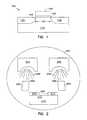
- FIG. 2depicts a deposition process in accordance with the present invention.
- FIG. 3depicts another configuration of a transistor capable of being fabricated in accordance with the present invention.
- FIG. 4depicts a perspective view of a personal computer incorporating devices made in accordance with the present invention.
- FIG. 5depicts a schematic view of a central processing unit incorporating devices made in accordance with the present invention.
- FIG. 6shows a schematic view of a DRAM memory device in accordance with the present invention.
- wafer and substrate used in the following descriptioninclude any structure having an exposed surface with which to form the integrated circuit (IC) structure of the invention.
- substrateis understood to include semiconductor wafers.
- substrateis also used to refer to semiconductor structures during processing, and may include other layers that have been fabricated thereupon. Both wafer and substrate include doped and undoped semiconductors, epitaxial semiconductor layers supported by a base semiconductor or insulator, as well as other semiconductor structures well known to one skilled in the art.
- conductoris understood to include semiconductors, and the term insulator or dielectric is defined to include any material that is less electrically conductive than the materials referred to as conductors.
- horizontalas used in this application is defined as a plane parallel to the conventional plane or surface of a wafer or substrate, regardless of the orientation of the wafer or substrate.
- verticalrefers to a direction perpendicular to the horizontal as defined above. Prepositions, such as “on”, “side” (as in “sidewall”), “higher”, “lower”, “over” and “under” are defined with respect to the conventional plane or surface being on the top surface of the wafer or substrate, regardless of the orientation of the wafer or substrate.
- Dielectric Constant Band gap Material( ⁇ ) E g (eV) Crystal Structure(s) SiO 2 3.9 8.9 Amorphous Si 3 N 4 7 5.1 Amorphous Al 2 O 3 9 8.7 Amorphous Y 2 O 3 15 5.6 Cubic La 2 O 3 30 4.3 Hexagonal, Cubic Ta 2 O 3 26 4.5 Orthorhombic TiO 2 80 3.5 Tetrag. (rutile, anatase) HfO 2 25 5.7 Mono., Tetrag., Cubic ZrO 2 25 7.8 Mono., Tetrag., Cubic
- SiO 2as a gate dielectric
- Having an amorphous structure for a gate dielectricis advantageous because grain boundaries in polycrystalline gate dielectrics provide high leakage paths. Additionally, grain size and orientation changes throughout a polycrystalline gate dielectric can cause variations in the film's dielectric constant.
- the abovementioned material properties including structureare for the materials in a bulk form.
- the materials having the advantage of a high dielectric constants relative to SiO 2also have the disadvantage of a crystalline form, at least in a bulk configuration.
- the best candidates for replacing SiO 2 as a gate dielectricare those with high dielectric constant, which can be fabricated as a thin layer with an amorphous form.
- a physical thickness of about 21 ⁇ of Al 2 O 3grown by thermal oxidation following thermal evaporation of an Al layer, could be obtained providing a t eq of 9.6 ⁇ with an interface state density greater than or equal to 3 ⁇ 10 10 eV ⁇ 1 cm ⁇ 2 .
- Higher physical thicknesses of about 48 ⁇ of Al 2 O 3provided films with t eq of 21 ⁇ with leakage current of approximately 10 ⁇ 8 A/cm 2 at 1 V gate bias, which is good when compared to a leakage current of 10 ⁇ 1 A/cm 2 at 1 V gate bias for a physical thickness of 21 ⁇ for a pure SiO 2 layer.
- La 2 O 3Another abovementioned material, La 2 O 3 , reportedly provided good results when fabricating thin films on silicon.
- Other studies on La 2 O 3showed reduced leakage current but an interfacial SiO x layer.
- the resultant filmswere determined to have a leakage current density decreased by about three orders of magnitude after annealing.
- This reported experimentation providing a LaAlO 3 buffer layer between silicon and a ferroelectric filmdemonstrated that a LaAlO 3 film could be obtained on silicon providing an amorphous dielectric layer with a dielectric constant between 21 and 24.
- Other reportsindicate that LaAlO 3 film can be grown by metal-organic chemical-vapor-deposition method, pulsed-laser depositions method, and rf magnetron sputtering method.
- layers of LaAlO 3can be deposited on silicon using low cost starting materials and resulting in dielectric layers whose dielectric constant can be chosen to range from the dielectric constant of Al 2 O 3 to the dielectric constant of La 2 O 3 .
- a layer of LaAlO 3is grown using dry pellets of Al 2 O 3 and La 2 O 3 .
- the gate dielectricis formed on a silicon substrate or silicon layer by electron beam evaporation of the dry pellets of using two electron guns controlled by two rate monitors. Controlling the rates for evaporating the dry pellets Al 2 O 3 and La 2 O 3 allows for the formation of a gate dielectric having a composition with a predetermined dielectric constant.
- the predetermined dielectric constantwill range from the dielectric constant of Al 2 O 3 to the dielectric constant of La 2 O 3 , depending on the composition of the film.
- the composition of the filmcan be shifted more towards an Al 2 O 3 film or more towards a La 2 O 3 film, depending upon the choice of the dielectric constant.
- FIG. 2depicts an electron beam evaporation technique to deposit a material forming a film containing LaAlO 3 on a surface such as a body region of a transistor.
- a substrate 210is placed inside a deposition chamber 260 .
- the substrate in this embodimentis masked by a first masking structure 270 and a second masking structure 271 .
- the unmasked region 233includes a body region of a transistor, however one skilled in the art will recognize that other semiconductor device structures may utilize this process.
- Also located within the deposition chamber 260is an electron gun 263 , a second electron gun 265 , a target 261 , and a second target 262 .
- the evaporation processcan be performed in chamber 260 using a base pressure lower than about 5 ⁇ 10 ⁇ 7 Torr and a deposition pressure less than about 2 ⁇ 10 ⁇ 6 Torr. Performing the evaporation under these conditions should allow a growth rate in the range from about 0.5 to about 50 nm/min.
- the wafer or substrate 210 containing the filmis annealed ex situ in an electric furnace at about 700° C. for about 10 minutes in N 2 ambience. Alternately, the wafer or substrate 210 can be annealed by RTA for about 10 to about 15 seconds in N 2 ambience.
- the LaAlO 3 dielectric filmshould have a dielectric constant in the range of about 21 to about 25.
- the composition of the filmcan vary from be a film of essentially Al 2 O 3 to a film that is essentially La 2 O 3 .
- the dielectric constant of the formed filmwill range from about 9 to about 30, with a dielectric constant in the range of about 21 to about 25 corresponding to a layer that is essentially LaAlO 3 .
- the two electron gunswill be controlled to formed a film containing Al 2 O 3 , La 2 O 3 , and LaAlO 3 in varying amounts depending on the setting for controlling the evaporation rates.
- a range of equivalent oxide thickness, t eq , attainable in accordance with the present inventionis associated with the capability to provide a composition having a dielectric constant in the range form about 9 to about 30, and the capability to attain growth rates in the range of from about 0.5 to about 50 nm/min.
- the t eq range in accordance with the present inventionare shown in the following
- LaAlO 3 in a bulk form at room temperaturehas a nearly cubic perovskite crystal structure with a lattice constant of 0.536 nm. Fortunately, the films grown by electron gun evaporation have an amorphous form, though it is expected that a dimension for a monolayer of LaAlO 3 is related to its lattice constant in bulk form. At a physical thickness about 0.5 nm, t eq would be expected to range from about 2.2 ⁇ to about 0.65 ⁇ for the dielectric constant ranging from 9 to 30. For a layer of essentially LaAlO 3 , t eq would be expected to range from about 0.93 ⁇ to about 0.78 ⁇ for a physical layer of 0.5 nm.
- t eqFor a substantially LaAlO 3 film having a thickness of approximately 2 nm, t eq would range from about 3 ⁇ to about 3.7 ⁇ . From above, it is apparent that a film containing LaAlO 3 can be attained with a t eq ranging from 1.5 ⁇ to 5 ⁇ . Further, such a film can provide a t eq significantly less than 2 or 3 ⁇ , even less than 1.5 ⁇ .
- the novel process described aboveprovides significant advantages by evaporating dry pellets of Al 2 O 3 and La 2 O 3 . Dry pellets of Al 2 O 3 and La 2 O 3 expensive than single crystal pellets of LaAlO 3 . Further, using two electron guns allows the formation of a gate dielectric with a chosen dielectric constant. Additionally, the novel process can be implemented to form transistors, memory devices, and information handling devices.
- a transistor 100 as depicted in FIG. 1can be formed by forming a source/drain region 120 and another source/drain region 130 in a silicon based substrate 110 where the two source/drain regions 120 , 130 are separated by a body region 132 .
- the body region 132 separated by the source/drain 120 and the source/drain 130defines a channel having a channel length 134 .
- Al 2 O 3is evaporated using an electron gun at a controlled rate.
- La 2 O 3is evaporated using a second electron gun at a second controlled rate. Evaporating the Al 2 O 3 source is begun substantially concurrent with evaporating La 2 O 3 , forming a film 140 containing LaAlO 3 on the body region.
- a gateis formed over the gate dielectric 140 .
- forming the gateincludes forming a polysilicon layer, though a metal gate can be formed in an alternative process.
- Forming the substrate, source/region regions, and the gateis performed using standard processes known to those skilled in the art. Additionally, the sequencing of the various elements of the process for forming a transistor is conducted with standard fabrication processes, also as known to those skilled in the art.
- the structure of FIG. 3depicts a transistor 300 having a silicon based substrate 310 with two source/drain regions 320 , 330 separated by a body region 332 .
- the body region 332 between the two source/drain regions 320 , 330defines a channel region having a channel length 334 .
- a stack 355including a gate dielectric 340 , a floating gate 352 , a floating gate dielectric 342 , and control gate 350 .
- Transistors created by the methods described abovemay be implemented into memory devices and information handling devices as shown in FIGS. 5-7 and described below. While specific types of memory devices and computing devices are shown below, it will be recognized by one skilled in the art that several types of memory devices and information handling devices could utilize the invention.
- a personal computeras shown in FIGS. 4 and 5 , include a monitor 400 , keyboard input 402 and a central processing unit 404 .
- the processor unittypically includes microprocessor 506 , memory bus circuit 508 having a plurality of memory slots 512 ( a-n ), and other peripheral circuitry 510 .
- Peripheral circuitry 510permits various peripheral devices 524 to interface processor-memory bus 520 over input/output (I/O) bus 522 .
- the personal computer shown in FIGS. 4 and 5also includes at least one transistor having a gate dielectric according to the teachings of the present invention.
- Coupled to memory bus 520are a plurality of memory slots 512 ( a-n ) which receive memory devices well known to those skilled in the art.
- memory slots 512a-n
- SIMMssingle in-line memory modules
- DIMMsdual in-line memory modules
- EDOextended data output
- DDR SDRAMDDR SDRAM
- SLDRAMDirect RDRAM
- SRAMFlash memories
- FIG. 6is a block diagram of an illustrative DRAM device 600 compatible with memory slots 512 ( a-n ).
- the description of DRAM 600has been simplified for purposes of illustrating a DRAM memory device and is not intended to be a complete description of all the features of a DRAM. Those skilled in the art will recognize that a wide variety of memory devices may be used in the implementation of the present invention.
- the example of a DRAM memory device shown in FIG. 6includes at least one transistor having a gate dielectric according to the teachings of the present invention.
- Row address buffer 612 and row decoder 614receive and decode row addresses from row address signals provided on address lines 604 by microprocessor 506 . Each unique row address corresponds to a row of cells in memory array 610 .
- Row decoder 614includes a wordline driver, an address decoder tree, and circuitry which translates a given row address received from row address buffers 612 and selectively activates the appropriate wordline of memory array 610 via the wordline drivers.
- Column address buffer 616 and column decoder 618receive and decode column address signals provided on address lines 604 .
- Column decoder 618also determines when a column is defective and the address of a replacement column.
- Column decoder 618is coupled to sense amplifiers 620 .
- Sense amplifiers 620are coupled to complementary pairs of bitlines of memory array 610 .
- Sense amplifiers 620are coupled to data-in buffer 622 and data-out buffer 624 .
- Data-in buffers 622 and data-out buffers 624are coupled to data lines 602 .
- data lines 602provide data to data-in buffer 622 .
- Sense amplifier 620receives data from data-in buffer 622 and stores the data in memory array 610 as a charge on a capacitor of a cell at an address specified on address lines 604 .
- Control logic 606is used to control the many available functions of DRAM 600 .
- various control circuits and signals not detailed hereininitiate and synchronize DRAM 600 operation as known to those skilled in the art.
- the description of DRAM 600has been simplified for purposes of illustrating the present invention and is not intended to be a complete description of all the features of a DRAM.
- memory devicesincluding but not limited to, SDRAMs, SLDRAMs, RDRAMs and other DRAMs and SRAMs, VRAMs and EEPROMs, may be used in the implementation of the present invention.
- the DRAM implementation described hereinis illustrative only and not intended to be exclusive or limiting.
- a gate dielectric containing LaAlO 3 and method of fabricating a gate dielectric contained LaAlO 3are provided that produces a reliable gate dielectric having a thinner equivalent oxide thickness than attainable using SiO 2 .
- LaAlO 3 gate dielectrics formed using the methods described hereinare thermodynamically stable such that the gate dielectrics formed will have minimal reactions with a silicon substrate or other structures during processing.
- Gate dielectric layers containing LaAlO 3are formed having a high dielectric constant ( ⁇ ) capable of a t eq thinner than 5 ⁇ , thinner than the expected limit for SiO 2 gate dielectrics.
- ⁇dielectric constant
- the physical thickness of the LaAlO 3 layeris much larger than the SiO 2 thickness associated with the t eq limit of SiO 2 . Forming the larger thickness provides advantages in processing the gate dielectric.
Landscapes
- Engineering & Computer Science (AREA)
- Computer Hardware Design (AREA)
- Power Engineering (AREA)
- Microelectronics & Electronic Packaging (AREA)
- Physics & Mathematics (AREA)
- Manufacturing & Machinery (AREA)
- Condensed Matter Physics & Semiconductors (AREA)
- General Physics & Mathematics (AREA)
- Chemical Kinetics & Catalysis (AREA)
- Chemical & Material Sciences (AREA)
- General Chemical & Material Sciences (AREA)
- Crystallography & Structural Chemistry (AREA)
- Insulated Gate Type Field-Effect Transistor (AREA)
- Thin Film Transistor (AREA)
- Semiconductor Memories (AREA)
Abstract
Description
t=(κ/κox)teq=(κ/3.9)teq.
Thus, materials with a dielectric constant greater than that of SiO2, 3.9, will have a physical thickness that can be considerably larger than a desired teq, while providing the desired equivalent oxide thickness. For example, an alternate dielectric material with a dielectric constant of 10 could have a thickness of about 25.6 Å to provide a teqof 10 Å, not including any depletion/inversion layer effects. Thus, the reduced equivalent oxide thickness of transistors can be realized by using dielectric materials with higher dielectric constants than SiO2.
| Dielectric Constant | Band gap | ||
| Material | (κ) | Eg(eV) | Crystal Structure(s) |
| SiO2 | 3.9 | 8.9 | Amorphous |
| Si3N4 | 7 | 5.1 | Amorphous |
| Al2O3 | 9 | 8.7 | Amorphous |
| Y2O3 | 15 | 5.6 | Cubic |
| La2O3 | 30 | 4.3 | Hexagonal, Cubic |
| Ta2O3 | 26 | 4.5 | Orthorhombic |
| TiO2 | 80 | 3.5 | Tetrag. (rutile, anatase) |
| HfO2 | 25 | 5.7 | Mono., Tetrag., Cubic |
| ZrO2 | 25 | 7.8 | Mono., Tetrag., Cubic |
| Physical Thickness | Physical Thickness | Physical Thickness | |
| t = 0.5 nm (5 Å) | t = 1.0 nm (10 Å) | t = 50 nm (500 Å) | |
| κ | teq(Å) | teq(Å) | teq(Å) |
| 9 | 2.17 | 4.33 | 216.67 |
| 21 | .93 | 1.86 | 92.86 |
| 25 | .78 | 1.56 | 78 |
| 30 | .65 | 1.3 | 65 |
Claims (43)
Priority Applications (2)
| Application Number | Priority Date | Filing Date | Title |
|---|---|---|---|
| US10/081,439US6893984B2 (en) | 2002-02-20 | 2002-02-20 | Evaporated LaA1O3 films for gate dielectrics |
| US11/059,594US20050145957A1 (en) | 2002-02-20 | 2005-02-16 | Evaporated LaAlO3 films for gate dielectrics |
Applications Claiming Priority (1)
| Application Number | Priority Date | Filing Date | Title |
|---|---|---|---|
| US10/081,439US6893984B2 (en) | 2002-02-20 | 2002-02-20 | Evaporated LaA1O3 films for gate dielectrics |
Related Child Applications (1)
| Application Number | Title | Priority Date | Filing Date |
|---|---|---|---|
| US11/059,594DivisionUS20050145957A1 (en) | 2002-02-20 | 2005-02-16 | Evaporated LaAlO3 films for gate dielectrics |
Publications (2)
| Publication Number | Publication Date |
|---|---|
| US20030157764A1 US20030157764A1 (en) | 2003-08-21 |
| US6893984B2true US6893984B2 (en) | 2005-05-17 |
Family
ID=27733266
Family Applications (2)
| Application Number | Title | Priority Date | Filing Date |
|---|---|---|---|
| US10/081,439Expired - LifetimeUS6893984B2 (en) | 2002-02-20 | 2002-02-20 | Evaporated LaA1O3 films for gate dielectrics |
| US11/059,594AbandonedUS20050145957A1 (en) | 2002-02-20 | 2005-02-16 | Evaporated LaAlO3 films for gate dielectrics |
Family Applications After (1)
| Application Number | Title | Priority Date | Filing Date |
|---|---|---|---|
| US11/059,594AbandonedUS20050145957A1 (en) | 2002-02-20 | 2005-02-16 | Evaporated LaAlO3 films for gate dielectrics |
Country Status (1)
| Country | Link |
|---|---|
| US (2) | US6893984B2 (en) |
Cited By (66)
| Publication number | Priority date | Publication date | Assignee | Title |
|---|---|---|---|---|
| US20030043637A1 (en)* | 2001-08-30 | 2003-03-06 | Micron Technology, Inc | Flash memory with low tunnel barrier interpoly insulators |
| US20040043569A1 (en)* | 2002-08-28 | 2004-03-04 | Ahn Kie Y. | Atomic layer deposited HfSiON dielectric films |
| US20040043541A1 (en)* | 2002-08-29 | 2004-03-04 | Ahn Kie Y. | Atomic layer deposited lanthanide doped TiOx dielectric films |
| US20040164365A1 (en)* | 2002-08-15 | 2004-08-26 | Micron Technology, Inc. | Lanthanide doped TiOx dielectric films |
| US20040185654A1 (en)* | 2001-12-20 | 2004-09-23 | Micron Technology, Inc. | Low-temperature growth high-quality ultra-thin praseodymium gate dielectrics |
| US20040214399A1 (en)* | 2003-04-22 | 2004-10-28 | Micron Technology, Inc. | Atomic layer deposited ZrTiO4 films |
| US20040262700A1 (en)* | 2003-06-24 | 2004-12-30 | Micron Technology, Inc. | Lanthanide oxide / hafnium oxide dielectrics |
| US20050020017A1 (en)* | 2003-06-24 | 2005-01-27 | Micron Technology, Inc. | Lanthanide oxide / hafnium oxide dielectric layers |
| US20050023627A1 (en)* | 2002-08-15 | 2005-02-03 | Micron Technology, Inc. | Lanthanide doped TiOx dielectric films by plasma oxidation |
| US7081421B2 (en) | 2004-08-26 | 2006-07-25 | Micron Technology, Inc. | Lanthanide oxide dielectric layer |
| US20060183272A1 (en)* | 2005-02-15 | 2006-08-17 | Micron Technology, Inc. | Atomic layer deposition of Zr3N4/ZrO2 films as gate dielectrics |
| US20060189154A1 (en)* | 2005-02-23 | 2006-08-24 | Micron Technology, Inc. | Atomic layer deposition of Hf3N4/HfO2 films as gate dielectrics |
| US7135421B2 (en) | 2002-06-05 | 2006-11-14 | Micron Technology, Inc. | Atomic layer-deposited hafnium aluminum oxide |
| US20060281330A1 (en)* | 2005-06-14 | 2006-12-14 | Micron Technology, Inc. | Iridium / zirconium oxide structure |
| US20070007635A1 (en)* | 2005-07-07 | 2007-01-11 | Micron Technology, Inc. | Self aligned metal gates on high-k dielectrics |
| US20070037415A1 (en)* | 2004-12-13 | 2007-02-15 | Micron Technology, Inc. | Lanthanum hafnium oxide dielectrics |
| US20070045752A1 (en)* | 2005-08-31 | 2007-03-01 | Leonard Forbes | Self aligned metal gates on high-K dielectrics |
| US20070049054A1 (en)* | 2005-08-31 | 2007-03-01 | Micron Technology, Inc. | Cobalt titanium oxide dielectric films |
| US7192892B2 (en) | 2003-03-04 | 2007-03-20 | Micron Technology, Inc. | Atomic layer deposited dielectric layers |
| US7205218B2 (en) | 2002-06-05 | 2007-04-17 | Micron Technology, Inc. | Method including forming gate dielectrics having multiple lanthanide oxide layers |
| US20070158702A1 (en)* | 2005-12-30 | 2007-07-12 | Doczy Mark L | Transistor including flatband voltage control through interface dipole engineering |
| US7259434B2 (en) | 2001-08-30 | 2007-08-21 | Micron Technology, Inc. | Highly reliable amorphous high-k gate oxide ZrO2 |
| US20080032062A1 (en)* | 2006-07-06 | 2008-02-07 | Meiere Scott H | Organometallic compounds having sterically hindered amides |
| US20080029790A1 (en)* | 2006-08-03 | 2008-02-07 | Micron Technology, Inc. | ALD of silicon films on germanium |
| US20080032424A1 (en)* | 2006-08-03 | 2008-02-07 | Micron Technology, Inc. | ALD of Zr-substituted BaTiO3 films as gate dielectrics |
| US20080054330A1 (en)* | 2006-08-31 | 2008-03-06 | Micron Technology, Inc. | Tantalum lanthanide oxynitride films |
| US20080087945A1 (en)* | 2006-08-31 | 2008-04-17 | Micron Technology, Inc. | Silicon lanthanide oxynitride films |
| US20080087890A1 (en)* | 2006-10-16 | 2008-04-17 | Micron Technology, Inc. | Methods to form dielectric structures in semiconductor devices and resulting devices |
| US7374964B2 (en) | 2005-02-10 | 2008-05-20 | Micron Technology, Inc. | Atomic layer deposition of CeO2/Al2O3 films as gate dielectrics |
| US7393736B2 (en) | 2005-08-29 | 2008-07-01 | Micron Technology, Inc. | Atomic layer deposition of Zrx Hfy Sn1-x-y O2 films as high k gate dielectrics |
| US7402876B2 (en) | 2002-12-04 | 2008-07-22 | Micron Technology, Inc. | Zr— Sn—Ti—O films |
| US7410668B2 (en) | 2001-03-01 | 2008-08-12 | Micron Technology, Inc. | Methods, systems, and apparatus for uniform chemical-vapor depositions |
| US7410910B2 (en) | 2005-08-31 | 2008-08-12 | Micron Technology, Inc. | Lanthanum aluminum oxynitride dielectric films |
| US7446368B2 (en) | 2001-08-30 | 2008-11-04 | Micron Technology, Inc. | Deposition of metal oxide and/or low asymmetrical tunnel barrier interpoly insulators |
| US20090004801A1 (en)* | 2007-06-28 | 2009-01-01 | Micron Technology, Inc. | Method of forming lutetium and lanthanum dielectric structures |
| US7494939B2 (en) | 2004-08-31 | 2009-02-24 | Micron Technology, Inc. | Methods for forming a lanthanum-metal oxide dielectric layer |
| US20090107586A1 (en)* | 2007-10-31 | 2009-04-30 | Kabushiki Kaisha Toshiba | Method for manufacturing a lanthanum oxide compound |
| US7544596B2 (en) | 2005-08-30 | 2009-06-09 | Micron Technology, Inc. | Atomic layer deposition of GdScO3 films as gate dielectrics |
| US7560395B2 (en) | 2005-01-05 | 2009-07-14 | Micron Technology, Inc. | Atomic layer deposited hafnium tantalum oxide dielectrics |
| US7560793B2 (en) | 2002-05-02 | 2009-07-14 | Micron Technology, Inc. | Atomic layer deposition and conversion |
| US7563730B2 (en) | 2006-08-31 | 2009-07-21 | Micron Technology, Inc. | Hafnium lanthanide oxynitride films |
| US7572695B2 (en) | 2005-05-27 | 2009-08-11 | Micron Technology, Inc. | Hafnium titanium oxide films |
| US7582161B2 (en) | 2006-04-07 | 2009-09-01 | Micron Technology, Inc. | Atomic layer deposited titanium-doped indium oxide films |
| US7582549B2 (en) | 2006-08-25 | 2009-09-01 | Micron Technology, Inc. | Atomic layer deposited barium strontium titanium oxide films |
| US7588988B2 (en) | 2004-08-31 | 2009-09-15 | Micron Technology, Inc. | Method of forming apparatus having oxide films formed using atomic layer deposition |
| US7601649B2 (en) | 2004-08-02 | 2009-10-13 | Micron Technology, Inc. | Zirconium-doped tantalum oxide films |
| US7605030B2 (en) | 2006-08-31 | 2009-10-20 | Micron Technology, Inc. | Hafnium tantalum oxynitride high-k dielectric and metal gates |
| US7611959B2 (en) | 2002-12-04 | 2009-11-03 | Micron Technology, Inc. | Zr-Sn-Ti-O films |
| US7625794B2 (en) | 2003-03-31 | 2009-12-01 | Micron Technology, Inc. | Methods of forming zirconium aluminum oxide |
| US7662729B2 (en) | 2005-04-28 | 2010-02-16 | Micron Technology, Inc. | Atomic layer deposition of a ruthenium layer to a lanthanide oxide dielectric layer |
| US7670646B2 (en) | 2002-05-02 | 2010-03-02 | Micron Technology, Inc. | Methods for atomic-layer deposition |
| US7687409B2 (en) | 2005-03-29 | 2010-03-30 | Micron Technology, Inc. | Atomic layer deposited titanium silicon oxide films |
| US7709402B2 (en) | 2006-02-16 | 2010-05-04 | Micron Technology, Inc. | Conductive layers for hafnium silicon oxynitride films |
| US7728626B2 (en) | 2002-07-08 | 2010-06-01 | Micron Technology, Inc. | Memory utilizing oxide nanolaminates |
| US7727908B2 (en) | 2006-08-03 | 2010-06-01 | Micron Technology, Inc. | Deposition of ZrA1ON films |
| US7759747B2 (en) | 2006-08-31 | 2010-07-20 | Micron Technology, Inc. | Tantalum aluminum oxynitride high-κ dielectric |
| US7776765B2 (en) | 2006-08-31 | 2010-08-17 | Micron Technology, Inc. | Tantalum silicon oxynitride high-k dielectrics and metal gates |
| US20100258881A1 (en)* | 2009-04-14 | 2010-10-14 | International Business Machines Corporation | Dual metal and dual dielectric integration for metal high-k fets |
| US7869242B2 (en) | 1999-07-30 | 2011-01-11 | Micron Technology, Inc. | Transmission lines for CMOS integrated circuits |
| US7972974B2 (en) | 2006-01-10 | 2011-07-05 | Micron Technology, Inc. | Gallium lanthanide oxide films |
| US8110469B2 (en) | 2005-08-30 | 2012-02-07 | Micron Technology, Inc. | Graded dielectric layers |
| US8125038B2 (en) | 2002-07-30 | 2012-02-28 | Micron Technology, Inc. | Nanolaminates of hafnium oxide and zirconium oxide |
| US8367506B2 (en) | 2007-06-04 | 2013-02-05 | Micron Technology, Inc. | High-k dielectrics with gold nano-particles |
| US8501563B2 (en) | 2005-07-20 | 2013-08-06 | Micron Technology, Inc. | Devices with nanocrystals and methods of formation |
| US20150129089A1 (en)* | 2013-11-13 | 2015-05-14 | The Government Of The United States Of America, As Represented By The Secretary Of The Navy | Hydrogen-Free Amorphous Dielectric Insulating Thin Films With No Tunneling States |
| US9741921B2 (en) | 2013-11-13 | 2017-08-22 | The United States Of America As Represented By The Secretary Of The Navy | Hydrogen free amorphous silicon as insulating dielectric material for superconducting quantum bits |
Families Citing this family (14)
| Publication number | Priority date | Publication date | Assignee | Title |
|---|---|---|---|---|
| US6844203B2 (en) | 2001-08-30 | 2005-01-18 | Micron Technology, Inc. | Gate oxides, and methods of forming |
| US6953730B2 (en) | 2001-12-20 | 2005-10-11 | Micron Technology, Inc. | Low-temperature grown high quality ultra-thin CoTiO3 gate dielectrics |
| US6767795B2 (en) | 2002-01-17 | 2004-07-27 | Micron Technology, Inc. | Highly reliable amorphous high-k gate dielectric ZrOXNY |
| US7045430B2 (en)* | 2002-05-02 | 2006-05-16 | Micron Technology Inc. | Atomic layer-deposited LaAlO3 films for gate dielectrics |
| US20050242387A1 (en)* | 2004-04-29 | 2005-11-03 | Micron Technology, Inc. | Flash memory device having a graded composition, high dielectric constant gate insulator |
| US7508648B2 (en)* | 2005-02-08 | 2009-03-24 | Micron Technology, Inc. | Atomic layer deposition of Dy doped HfO2 films as gate dielectrics |
| US7365027B2 (en) | 2005-03-29 | 2008-04-29 | Micron Technology, Inc. | ALD of amorphous lanthanide doped TiOx films |
| US7390756B2 (en)* | 2005-04-28 | 2008-06-24 | Micron Technology, Inc. | Atomic layer deposited zirconium silicon oxide films |
| JP2007053171A (en)* | 2005-08-16 | 2007-03-01 | Toshiba Corp | Nonvolatile semiconductor memory device |
| JP5057834B2 (en)* | 2007-04-25 | 2012-10-24 | 株式会社東芝 | Method for producing lanthanoid aluminate film |
| US7760541B2 (en)* | 2008-08-12 | 2010-07-20 | International Business Machines Corporation | Functional float mode screen to test for leakage defects on SRAM bitlines |
| TWI445166B (en)* | 2008-11-07 | 2014-07-11 | Sony Corp | Solid-state imaging device, method of manufacturing solid-state imaging device, and electronic device |
| TWI889225B (en)* | 2021-06-03 | 2025-07-01 | 瑞礱科技股份有限公司 | Gate dielectric and manufacturing method |
| TWI849316B (en)* | 2021-06-03 | 2024-07-21 | 瑞礱科技股份有限公司 | Gate dielectric and manufacturing method |
Citations (40)
| Publication number | Priority date | Publication date | Assignee | Title |
|---|---|---|---|---|
| US4394673A (en) | 1980-09-29 | 1983-07-19 | International Business Machines Corporation | Rare earth silicide Schottky barriers |
| US5302461A (en) | 1992-06-05 | 1994-04-12 | Hewlett-Packard Company | Dielectric films for use in magnetoresistive transducers |
| US5625233A (en) | 1995-01-13 | 1997-04-29 | Ibm Corporation | Thin film multi-layer oxygen diffusion barrier consisting of refractory metal, refractory metal aluminide, and aluminum oxide |
| US5698022A (en) | 1996-08-14 | 1997-12-16 | Advanced Technology Materials, Inc. | Lanthanide/phosphorus precursor compositions for MOCVD of lanthanide/phosphorus oxide films |
| US5801105A (en) | 1995-08-04 | 1998-09-01 | Tdk Corporation | Multilayer thin film, substrate for electronic device, electronic device, and preparation of multilayer oxide thin film |
| US5810923A (en) | 1994-08-17 | 1998-09-22 | Tdk Corporation | Method for forming oxide thin film and the treatment of silicon substrate |
| US5840897A (en) | 1990-07-06 | 1998-11-24 | Advanced Technology Materials, Inc. | Metal complex source reagents for chemical vapor deposition |
| US6040243A (en) | 1999-09-20 | 2000-03-21 | Chartered Semiconductor Manufacturing Ltd. | Method to form copper damascene interconnects using a reverse barrier metal scheme to eliminate copper diffusion |
| US6057271A (en) | 1989-12-22 | 2000-05-02 | Sumitomo Electric Industries, Ltd. | Method of making a superconducting microwave component by off-axis sputtering |
| US6093944A (en) | 1998-06-04 | 2000-07-25 | Lucent Technologies Inc. | Dielectric materials of amorphous compositions of TI-O2 doped with rare earth elements and devices employing same |
| US6110529A (en) | 1990-07-06 | 2000-08-29 | Advanced Tech Materials | Method of forming metal films on a substrate by chemical vapor deposition |
| US6203613B1 (en) | 1999-10-19 | 2001-03-20 | International Business Machines Corporation | Atomic layer deposition with nitrate containing precursors |
| US6203726B1 (en)* | 1997-03-04 | 2001-03-20 | Symyx Technologies, Inc. | Phosphor Materials |
| US6207589B1 (en) | 1999-07-19 | 2001-03-27 | Sharp Laboratories Of America, Inc. | Method of forming a doped metal oxide dielectric film |
| EP1096042A1 (en) | 1999-10-25 | 2001-05-02 | Motorola, Inc. | Method for fabricating a semiconductor structure including a metal oxide interface with silicon |
| US6297539B1 (en) | 1999-07-19 | 2001-10-02 | Sharp Laboratories Of America, Inc. | Doped zirconia, or zirconia-like, dielectric film transistor structure and deposition method for same |
| US6300203B1 (en) | 2000-10-05 | 2001-10-09 | Advanced Micro Devices, Inc. | Electrolytic deposition of dielectric precursor materials for use in in-laid gate MOS transistors |
| WO2002031875A2 (en) | 2000-10-10 | 2002-04-18 | Asm America, Inc. | Dielectric interface films and methods therefor |
| US6387712B1 (en) | 1996-06-26 | 2002-05-14 | Tdk Corporation | Process for preparing ferroelectric thin films |
| US20020089023A1 (en) | 2001-01-05 | 2002-07-11 | Motorola, Inc. | Low leakage current metal oxide-nitrides and method of fabricating same |
| US6432779B1 (en) | 2000-05-18 | 2002-08-13 | Motorola, Inc. | Selective removal of a metal oxide dielectric |
| US6451662B1 (en) | 2001-10-04 | 2002-09-17 | International Business Machines Corporation | Method of forming low-leakage on-chip capacitor |
| US6461914B1 (en) | 2001-08-29 | 2002-10-08 | Motorola, Inc. | Process for making a MIM capacitor |
| US20020146916A1 (en) | 2001-03-29 | 2002-10-10 | Kiyoshi Irino | Semiconductor device having a high-dielectric gate insulation film and fabrication process thereof |
| US6465334B1 (en) | 2000-10-05 | 2002-10-15 | Advanced Micro Devices, Inc. | Enhanced electroless deposition of dielectric precursor materials for use in in-laid gate MOS transistors |
| US20020155689A1 (en) | 2001-04-20 | 2002-10-24 | Ahn Kie Y. | Highly reliable gate oxide and method of fabrication |
| US6495436B2 (en) | 2001-02-09 | 2002-12-17 | Micron Technology, Inc. | Formation of metal oxide gate dielectric |
| US20020192974A1 (en) | 2001-06-13 | 2002-12-19 | Ahn Kie Y. | Dielectric layer forming method and devices formed therewith |
| US20030017717A1 (en) | 2001-07-18 | 2003-01-23 | Ahn Kie Y. | Methods for forming dielectric materials and methods for forming semiconductor devices |
| US6521911B2 (en) | 2000-07-20 | 2003-02-18 | North Carolina State University | High dielectric constant metal silicates formed by controlled metal-surface reactions |
| US6527866B1 (en)* | 2000-02-09 | 2003-03-04 | Conductus, Inc. | Apparatus and method for deposition of thin films |
| US6531354B2 (en) | 2000-01-19 | 2003-03-11 | North Carolina State University | Lanthanum oxide-based gate dielectrics for integrated circuit field effect transistors |
| US20030119291A1 (en) | 2001-12-20 | 2003-06-26 | Micron Technology, Inc. | Low-temperature grown high-quality ultra-thin praseodymium gate dielectrics |
| US6620670B2 (en) | 2002-01-18 | 2003-09-16 | Applied Materials, Inc. | Process conditions and precursors for atomic layer deposition (ALD) of AL2O3 |
| US6627503B2 (en) | 2000-02-11 | 2003-09-30 | Sharp Laboratories Of America, Inc. | Method of forming a multilayer dielectric stack |
| US20030207593A1 (en) | 2002-05-02 | 2003-11-06 | Micron Technology, Inc. | Atomic layer deposition and conversion |
| US6645882B1 (en)* | 2002-01-17 | 2003-11-11 | Advanced Micro Devices, Inc. | Preparation of composite high-K/standard-K dielectrics for semiconductor devices |
| US6683011B2 (en) | 2001-11-14 | 2004-01-27 | Regents Of The University Of Minnesota | Process for forming hafnium oxide films |
| US6696332B2 (en) | 2001-12-26 | 2004-02-24 | Texas Instruments Incorporated | Bilayer deposition to avoid unwanted interfacial reactions during high K gate dielectric processing |
| US6699745B1 (en) | 1997-03-27 | 2004-03-02 | Texas Instruments Incorporated | Capacitor and memory structure and method |
Family Cites Families (65)
| Publication number | Priority date | Publication date | Assignee | Title |
|---|---|---|---|---|
| US4725877A (en)* | 1986-04-11 | 1988-02-16 | American Telephone And Telegraph Company, At&T Bell Laboratories | Metallized semiconductor device including an interface layer |
| US5304622A (en)* | 1992-01-08 | 1994-04-19 | Nippon Oil Company, Ltd. | Process for producing polysilanes |
| TW235363B (en)* | 1993-01-25 | 1994-12-01 | Hitachi Seisakusyo Kk | |
| US6210537B1 (en)* | 1995-06-19 | 2001-04-03 | Lynntech, Inc. | Method of forming electronically conducting polymers on conducting and nonconducting substrates |
| US5777923A (en)* | 1996-06-17 | 1998-07-07 | Aplus Integrated Circuits, Inc. | Flash memory read/write controller |
| US6173379B1 (en)* | 1996-05-14 | 2001-01-09 | Intel Corporation | Memory device for a microprocessor register file having a power management scheme and method for copying information between memory sub-cells in a single clock cycle |
| US6267529B1 (en)* | 1996-10-04 | 2001-07-31 | Rondo Building Services Pty. Ltd. | Flexible traffic post |
| US5923056A (en)* | 1996-10-10 | 1999-07-13 | Lucent Technologies Inc. | Electronic components with doped metal oxide dielectric materials and a process for making electronic components with doped metal oxide dielectric materials |
| US6075691A (en)* | 1997-03-06 | 2000-06-13 | Lucent Technologies Inc. | Thin film capacitors and process for making them |
| US6034015A (en)* | 1997-05-14 | 2000-03-07 | Georgia Tech Research Corporation | Ceramic compositions for microwave wireless communication |
| US6350672B1 (en)* | 1997-07-28 | 2002-02-26 | United Microelectronics Corp. | Interconnect structure with gas dielectric compatible with unlanded vias |
| US6020024A (en)* | 1997-08-04 | 2000-02-01 | Motorola, Inc. | Method for forming high dielectric constant metal oxides |
| US6333556B1 (en)* | 1997-10-09 | 2001-12-25 | Micron Technology, Inc. | Insulating materials |
| KR100269328B1 (en)* | 1997-12-31 | 2000-10-16 | 윤종용 | Method for forming conductive layer using atomic layer deposition process |
| US6225237B1 (en)* | 1998-09-01 | 2001-05-01 | Micron Technology, Inc. | Method for forming metal-containing films using metal complexes with chelating O- and/or N-donor ligands |
| US6207522B1 (en)* | 1998-11-23 | 2001-03-27 | Microcoating Technologies | Formation of thin film capacitors |
| US6383861B1 (en)* | 1999-02-18 | 2002-05-07 | Micron Technology, Inc. | Method of fabricating a dual gate dielectric |
| US6436801B1 (en)* | 1999-02-26 | 2002-08-20 | Texas Instruments Incorporated | Hafnium nitride gate dielectric |
| US6709968B1 (en)* | 2000-08-16 | 2004-03-23 | Micron Technology, Inc. | Microelectronic device with package with conductive elements and associated method of manufacture |
| FI117942B (en)* | 1999-10-14 | 2007-04-30 | Asm Int | Process for making oxide thin films |
| US6392257B1 (en)* | 2000-02-10 | 2002-05-21 | Motorola Inc. | Semiconductor structure, semiconductor device, communicating device, integrated circuit, and process for fabricating the same |
| DE10010821A1 (en)* | 2000-02-29 | 2001-09-13 | Infineon Technologies Ag | Method for increasing the capacitance in a storage trench and trench capacitor with increased capacitance |
| US6537613B1 (en)* | 2000-04-10 | 2003-03-25 | Air Products And Chemicals, Inc. | Process for metal metalloid oxides and nitrides with compositional gradients |
| US6984591B1 (en)* | 2000-04-20 | 2006-01-10 | International Business Machines Corporation | Precursor source mixtures |
| US6573160B2 (en)* | 2000-05-26 | 2003-06-03 | Motorola, Inc. | Method of recrystallizing an amorphous region of a semiconductor |
| US7217615B1 (en)* | 2000-08-31 | 2007-05-15 | Micron Technology, Inc. | Capacitor fabrication methods including forming a conductive layer |
| US6541353B1 (en)* | 2000-08-31 | 2003-04-01 | Micron Technology, Inc. | Atomic layer doping apparatus and method |
| US6420230B1 (en)* | 2000-08-31 | 2002-07-16 | Micron Technology, Inc. | Capacitor fabrication methods and capacitor constructions |
| US6395650B1 (en)* | 2000-10-23 | 2002-05-28 | International Business Machines Corporation | Methods for forming metal oxide layers with enhanced purity |
| US7476420B2 (en)* | 2000-10-23 | 2009-01-13 | Asm International N.V. | Process for producing metal oxide films at low temperatures |
| KR20020056260A (en)* | 2000-12-29 | 2002-07-10 | 박종섭 | Method for forming metal gate of semiconductor devoie |
| KR100385952B1 (en)* | 2001-01-19 | 2003-06-02 | 삼성전자주식회사 | A semiconductor capacitor having tantalum oxide as dielctric film and formation method thereof |
| US6713846B1 (en)* | 2001-01-26 | 2004-03-30 | Aviza Technology, Inc. | Multilayer high κ dielectric films |
| US6844604B2 (en)* | 2001-02-02 | 2005-01-18 | Samsung Electronics Co., Ltd. | Dielectric layer for semiconductor device and method of manufacturing the same |
| US6613656B2 (en)* | 2001-02-13 | 2003-09-02 | Micron Technology, Inc. | Sequential pulse deposition |
| US6541280B2 (en)* | 2001-03-20 | 2003-04-01 | Motorola, Inc. | High K dielectric film |
| US6602720B2 (en)* | 2001-03-28 | 2003-08-05 | Sharp Laboratories Of America, Inc. | Single transistor ferroelectric transistor structure with high-K insulator and method of fabricating same |
| KR100426219B1 (en)* | 2001-05-18 | 2004-04-06 | 홍국선 | Dielectric Ceramic Compositions and Manufacturing Method of Multilayer components thereof |
| US7037574B2 (en)* | 2001-05-23 | 2006-05-02 | Veeco Instruments, Inc. | Atomic layer deposition for fabricating thin films |
| KR20030018134A (en)* | 2001-08-27 | 2003-03-06 | 한국전자통신연구원 | Method of forming an insulation layer of a semiconductor device for controlling the composition and the doping concentration |
| US7068544B2 (en)* | 2001-08-30 | 2006-06-27 | Micron Technology, Inc. | Flash memory with low tunnel barrier interpoly insulators |
| US6730575B2 (en)* | 2001-08-30 | 2004-05-04 | Micron Technology, Inc. | Methods of forming perovskite-type material and capacitor dielectric having perovskite-type crystalline structure |
| US7476925B2 (en)* | 2001-08-30 | 2009-01-13 | Micron Technology, Inc. | Atomic layer deposition of metal oxide and/or low asymmetrical tunnel barrier interploy insulators |
| US7160817B2 (en)* | 2001-08-30 | 2007-01-09 | Micron Technology, Inc. | Dielectric material forming methods |
| US6605549B2 (en)* | 2001-09-29 | 2003-08-12 | Intel Corporation | Method for improving nucleation and adhesion of CVD and ALD films deposited onto low-dielectric-constant dielectrics |
| US6720259B2 (en)* | 2001-10-02 | 2004-04-13 | Genus, Inc. | Passivation method for improved uniformity and repeatability for atomic layer deposition and chemical vapor deposition |
| US6562491B1 (en)* | 2001-10-15 | 2003-05-13 | Advanced Micro Devices, Inc. | Preparation of composite high-K dielectrics |
| US6559014B1 (en)* | 2001-10-15 | 2003-05-06 | Advanced Micro Devices, Inc. | Preparation of composite high-K / standard-K dielectrics for semiconductor devices |
| US6514808B1 (en)* | 2001-11-30 | 2003-02-04 | Motorola, Inc. | Transistor having a high K dielectric and short gate length and method therefor |
| US6674138B1 (en)* | 2001-12-31 | 2004-01-06 | Advanced Micro Devices, Inc. | Use of high-k dielectric materials in modified ONO structure for semiconductor devices |
| US6528858B1 (en)* | 2002-01-11 | 2003-03-04 | Advanced Micro Devices, Inc. | MOSFETs with differing gate dielectrics and method of formation |
| US7205218B2 (en)* | 2002-06-05 | 2007-04-17 | Micron Technology, Inc. | Method including forming gate dielectrics having multiple lanthanide oxide layers |
| US6790791B2 (en)* | 2002-08-15 | 2004-09-14 | Micron Technology, Inc. | Lanthanide doped TiOx dielectric films |
| US7199023B2 (en)* | 2002-08-28 | 2007-04-03 | Micron Technology, Inc. | Atomic layer deposited HfSiON dielectric films wherein each precursor is independendently pulsed |
| US7084078B2 (en)* | 2002-08-29 | 2006-08-01 | Micron Technology, Inc. | Atomic layer deposited lanthanide doped TiOx dielectric films |
| US7494939B2 (en)* | 2004-08-31 | 2009-02-24 | Micron Technology, Inc. | Methods for forming a lanthanum-metal oxide dielectric layer |
| US7235501B2 (en)* | 2004-12-13 | 2007-06-26 | Micron Technology, Inc. | Lanthanum hafnium oxide dielectrics |
| US7365027B2 (en)* | 2005-03-29 | 2008-04-29 | Micron Technology, Inc. | ALD of amorphous lanthanide doped TiOx films |
| US7606816B2 (en)* | 2005-06-03 | 2009-10-20 | Yahoo! Inc. | Record boundary identification and extraction through pattern mining |
| US7195999B2 (en)* | 2005-07-07 | 2007-03-27 | Micron Technology, Inc. | Metal-substituted transistor gates |
| US20070018214A1 (en)* | 2005-07-25 | 2007-01-25 | Micron Technology, Inc. | Magnesium titanium oxide films |
| US7575978B2 (en)* | 2005-08-04 | 2009-08-18 | Micron Technology, Inc. | Method for making conductive nanoparticle charge storage element |
| US7393736B2 (en)* | 2005-08-29 | 2008-07-01 | Micron Technology, Inc. | Atomic layer deposition of Zrx Hfy Sn1-x-y O2 films as high k gate dielectrics |
| US20070049023A1 (en)* | 2005-08-29 | 2007-03-01 | Micron Technology, Inc. | Zirconium-doped gadolinium oxide films |
| US7214994B2 (en)* | 2005-08-31 | 2007-05-08 | Micron Technology, Inc. | Self aligned metal gates on high-k dielectrics |
- 2002
- 2002-02-20USUS10/081,439patent/US6893984B2/ennot_activeExpired - Lifetime
- 2005
- 2005-02-16USUS11/059,594patent/US20050145957A1/ennot_activeAbandoned
Patent Citations (44)
| Publication number | Priority date | Publication date | Assignee | Title |
|---|---|---|---|---|
| US4394673A (en) | 1980-09-29 | 1983-07-19 | International Business Machines Corporation | Rare earth silicide Schottky barriers |
| US6057271A (en) | 1989-12-22 | 2000-05-02 | Sumitomo Electric Industries, Ltd. | Method of making a superconducting microwave component by off-axis sputtering |
| US5840897A (en) | 1990-07-06 | 1998-11-24 | Advanced Technology Materials, Inc. | Metal complex source reagents for chemical vapor deposition |
| US6110529A (en) | 1990-07-06 | 2000-08-29 | Advanced Tech Materials | Method of forming metal films on a substrate by chemical vapor deposition |
| US5302461A (en) | 1992-06-05 | 1994-04-12 | Hewlett-Packard Company | Dielectric films for use in magnetoresistive transducers |
| US5828080A (en) | 1994-08-17 | 1998-10-27 | Tdk Corporation | Oxide thin film, electronic device substrate and electronic device |
| US5810923A (en) | 1994-08-17 | 1998-09-22 | Tdk Corporation | Method for forming oxide thin film and the treatment of silicon substrate |
| US5625233A (en) | 1995-01-13 | 1997-04-29 | Ibm Corporation | Thin film multi-layer oxygen diffusion barrier consisting of refractory metal, refractory metal aluminide, and aluminum oxide |
| US5801105A (en) | 1995-08-04 | 1998-09-01 | Tdk Corporation | Multilayer thin film, substrate for electronic device, electronic device, and preparation of multilayer oxide thin film |
| US6387712B1 (en) | 1996-06-26 | 2002-05-14 | Tdk Corporation | Process for preparing ferroelectric thin films |
| US5698022A (en) | 1996-08-14 | 1997-12-16 | Advanced Technology Materials, Inc. | Lanthanide/phosphorus precursor compositions for MOCVD of lanthanide/phosphorus oxide films |
| US6203726B1 (en)* | 1997-03-04 | 2001-03-20 | Symyx Technologies, Inc. | Phosphor Materials |
| US6699745B1 (en) | 1997-03-27 | 2004-03-02 | Texas Instruments Incorporated | Capacitor and memory structure and method |
| US6093944A (en) | 1998-06-04 | 2000-07-25 | Lucent Technologies Inc. | Dielectric materials of amorphous compositions of TI-O2 doped with rare earth elements and devices employing same |
| US6207589B1 (en) | 1999-07-19 | 2001-03-27 | Sharp Laboratories Of America, Inc. | Method of forming a doped metal oxide dielectric film |
| US6297539B1 (en) | 1999-07-19 | 2001-10-02 | Sharp Laboratories Of America, Inc. | Doped zirconia, or zirconia-like, dielectric film transistor structure and deposition method for same |
| US6040243A (en) | 1999-09-20 | 2000-03-21 | Chartered Semiconductor Manufacturing Ltd. | Method to form copper damascene interconnects using a reverse barrier metal scheme to eliminate copper diffusion |
| US6203613B1 (en) | 1999-10-19 | 2001-03-20 | International Business Machines Corporation | Atomic layer deposition with nitrate containing precursors |
| EP1096042A1 (en) | 1999-10-25 | 2001-05-02 | Motorola, Inc. | Method for fabricating a semiconductor structure including a metal oxide interface with silicon |
| US6531354B2 (en) | 2000-01-19 | 2003-03-11 | North Carolina State University | Lanthanum oxide-based gate dielectrics for integrated circuit field effect transistors |
| US6527866B1 (en)* | 2000-02-09 | 2003-03-04 | Conductus, Inc. | Apparatus and method for deposition of thin films |
| US6627503B2 (en) | 2000-02-11 | 2003-09-30 | Sharp Laboratories Of America, Inc. | Method of forming a multilayer dielectric stack |
| US6432779B1 (en) | 2000-05-18 | 2002-08-13 | Motorola, Inc. | Selective removal of a metal oxide dielectric |
| US6521911B2 (en) | 2000-07-20 | 2003-02-18 | North Carolina State University | High dielectric constant metal silicates formed by controlled metal-surface reactions |
| US6300203B1 (en) | 2000-10-05 | 2001-10-09 | Advanced Micro Devices, Inc. | Electrolytic deposition of dielectric precursor materials for use in in-laid gate MOS transistors |
| US6465334B1 (en) | 2000-10-05 | 2002-10-15 | Advanced Micro Devices, Inc. | Enhanced electroless deposition of dielectric precursor materials for use in in-laid gate MOS transistors |
| WO2002031875A2 (en) | 2000-10-10 | 2002-04-18 | Asm America, Inc. | Dielectric interface films and methods therefor |
| US20020089023A1 (en) | 2001-01-05 | 2002-07-11 | Motorola, Inc. | Low leakage current metal oxide-nitrides and method of fabricating same |
| US6495436B2 (en) | 2001-02-09 | 2002-12-17 | Micron Technology, Inc. | Formation of metal oxide gate dielectric |
| US20020146916A1 (en) | 2001-03-29 | 2002-10-10 | Kiyoshi Irino | Semiconductor device having a high-dielectric gate insulation film and fabrication process thereof |
| US6514828B2 (en) | 2001-04-20 | 2003-02-04 | Micron Technology, Inc. | Method of fabricating a highly reliable gate oxide |
| US20020155688A1 (en) | 2001-04-20 | 2002-10-24 | Ahn Kie Y. | Highly reliable gate oxide and method of fabrication |
| US20020155689A1 (en) | 2001-04-20 | 2002-10-24 | Ahn Kie Y. | Highly reliable gate oxide and method of fabrication |
| US20020192974A1 (en) | 2001-06-13 | 2002-12-19 | Ahn Kie Y. | Dielectric layer forming method and devices formed therewith |
| US6534420B2 (en) | 2001-07-18 | 2003-03-18 | Micron Technology, Inc. | Methods for forming dielectric materials and methods for forming semiconductor devices |
| US20030017717A1 (en) | 2001-07-18 | 2003-01-23 | Ahn Kie Y. | Methods for forming dielectric materials and methods for forming semiconductor devices |
| US6461914B1 (en) | 2001-08-29 | 2002-10-08 | Motorola, Inc. | Process for making a MIM capacitor |
| US6451662B1 (en) | 2001-10-04 | 2002-09-17 | International Business Machines Corporation | Method of forming low-leakage on-chip capacitor |
| US6683011B2 (en) | 2001-11-14 | 2004-01-27 | Regents Of The University Of Minnesota | Process for forming hafnium oxide films |
| US20030119291A1 (en) | 2001-12-20 | 2003-06-26 | Micron Technology, Inc. | Low-temperature grown high-quality ultra-thin praseodymium gate dielectrics |
| US6696332B2 (en) | 2001-12-26 | 2004-02-24 | Texas Instruments Incorporated | Bilayer deposition to avoid unwanted interfacial reactions during high K gate dielectric processing |
| US6645882B1 (en)* | 2002-01-17 | 2003-11-11 | Advanced Micro Devices, Inc. | Preparation of composite high-K/standard-K dielectrics for semiconductor devices |
| US6620670B2 (en) | 2002-01-18 | 2003-09-16 | Applied Materials, Inc. | Process conditions and precursors for atomic layer deposition (ALD) of AL2O3 |
| US20030207593A1 (en) | 2002-05-02 | 2003-11-06 | Micron Technology, Inc. | Atomic layer deposition and conversion |
Non-Patent Citations (12)
| Title |
|---|
| Bunshad, Rointan F., et al., "Deposition Technologies for Films and Coatings: Developments and Applications", Park Ridge, N.J., U.S.A. : Noyes Publications, (1992), 102-103. |
| Geller, S., et al., "Crystallographic Studies of Perovskite-like Compounds. II. Rare Earth Aluminates", Acta Cryst. vol. 9, (1956), pp. 1019-1025. |
| Giess, E.A., et al., "Lanthanide gallate perovskite-type substrates for epitaxial, high-T<SUB>c </SUB>superconducting Ba<SUB>2</SUB>YCu<SUB>3</SUB>O<SUB>7-delta</SUB> films", IBM J. Res. Develop. vol. 34, No. 6, (Nov. 6, 1990), pp. 916-926. |
| Kim, D., et al., "Atomic Control of Substrate Termination and Heteroepitaxial Growth of SrTiO3/LaAIO3 Films", Journal of the Korean Phyical Society, 36(6), (Jun. 2000), 444-448. |
| Lee, A.E., et al., "Epitaxially grown sputtered LaA1O<SUB>3 </SUB>films", Appl. Phys. Lett. 57 (19), (Nov. 5, 1990), pp. 2019-2021. |
| Lee, L.P., et al., "Monolithic 77 K dc SQUID magnetometer", Appl. Phys. Lett. 59 (23), (Dec. 2, 1991), pp. 3051-3053. |
| Molodyk, A. A., et al., "Volatile Surfactant-Assisted MOCVD: Application to LaA1O<SUB>3 </SUB>Thin Film Growth", Chem. Vap. Deposition vol. 6, No. 3, (2000), pp. 133-138. |
| Ohmi, S., et al., "Rare Earth Metal Oxides for High-K Gate Insulator", Electrochemical Society Proceedings, vol. 2002-2, (2002), 376-387. |
| Park, Byung-Eun, et al., "Electrical properties of LaA1O<SUB>3</SUB>/Si and Sr<SUB>0.8</SUB>Bi<SUB>2.2</SUB>Ta<SUB>2</SUB>O<SUB>9</SUB>/LaA1O<SUB>3</SUB>/Si structures", Applied Physics Letters, vol. 79, No. 6, (Aug. 6, 2001), pp. 806-808. |
| Takemoto, J.H., et al., "Microstrip Resonators and Filters Using High-TC Superconducting Thin Films on LaA1O<SUB>3</SUB>", IEEE Transactions on Magnetics, vol. 27, No. 2, (Mar., 1991), pp. 2549-2552. |
| Wilk, G.D., et al., "High-kappa gate dielectrics: Current status and materials properties considerations", J. Appl. Phys., vol. 89, No. 10, (May 15, 2001), pp. 5243-5275. |
| Wolf, S., et al., In:Silicon Processing of the VLSI Era vol. 1, Lattic Press, 374-380. |
Cited By (187)
| Publication number | Priority date | Publication date | Assignee | Title |
|---|---|---|---|---|
| US7869242B2 (en) | 1999-07-30 | 2011-01-11 | Micron Technology, Inc. | Transmission lines for CMOS integrated circuits |
| US7410668B2 (en) | 2001-03-01 | 2008-08-12 | Micron Technology, Inc. | Methods, systems, and apparatus for uniform chemical-vapor depositions |
| US7476925B2 (en) | 2001-08-30 | 2009-01-13 | Micron Technology, Inc. | Atomic layer deposition of metal oxide and/or low asymmetrical tunnel barrier interploy insulators |
| US7259434B2 (en) | 2001-08-30 | 2007-08-21 | Micron Technology, Inc. | Highly reliable amorphous high-k gate oxide ZrO2 |
| US8652957B2 (en) | 2001-08-30 | 2014-02-18 | Micron Technology, Inc. | High-K gate dielectric oxide |
| US7545674B2 (en) | 2001-08-30 | 2009-06-09 | Micron Technology, Inc. | Flash memory with low tunnel barrier interpoly insulators |
| US8026161B2 (en) | 2001-08-30 | 2011-09-27 | Micron Technology, Inc. | Highly reliable amorphous high-K gate oxide ZrO2 |
| US7446368B2 (en) | 2001-08-30 | 2008-11-04 | Micron Technology, Inc. | Deposition of metal oxide and/or low asymmetrical tunnel barrier interpoly insulators |
| US7068544B2 (en) | 2001-08-30 | 2006-06-27 | Micron Technology, Inc. | Flash memory with low tunnel barrier interpoly insulators |
| US20030043637A1 (en)* | 2001-08-30 | 2003-03-06 | Micron Technology, Inc | Flash memory with low tunnel barrier interpoly insulators |
| US6979855B2 (en) | 2001-12-20 | 2005-12-27 | Micron Technology, Inc. | High-quality praseodymium gate dielectrics |
| US7064058B2 (en) | 2001-12-20 | 2006-06-20 | Micron Technology, Inc. | Low-temperature growth high-quality ultra-thin praseodymium gate dieletrics |
| US20040185654A1 (en)* | 2001-12-20 | 2004-09-23 | Micron Technology, Inc. | Low-temperature growth high-quality ultra-thin praseodymium gate dielectrics |
| US7670646B2 (en) | 2002-05-02 | 2010-03-02 | Micron Technology, Inc. | Methods for atomic-layer deposition |
| US7589029B2 (en) | 2002-05-02 | 2009-09-15 | Micron Technology, Inc. | Atomic layer deposition and conversion |
| US7560793B2 (en) | 2002-05-02 | 2009-07-14 | Micron Technology, Inc. | Atomic layer deposition and conversion |
| US7205218B2 (en) | 2002-06-05 | 2007-04-17 | Micron Technology, Inc. | Method including forming gate dielectrics having multiple lanthanide oxide layers |
| US7554161B2 (en) | 2002-06-05 | 2009-06-30 | Micron Technology, Inc. | HfAlO3 films for gate dielectrics |
| US7135421B2 (en) | 2002-06-05 | 2006-11-14 | Micron Technology, Inc. | Atomic layer-deposited hafnium aluminum oxide |
| US8093638B2 (en) | 2002-06-05 | 2012-01-10 | Micron Technology, Inc. | Systems with a gate dielectric having multiple lanthanide oxide layers |
| US8228725B2 (en) | 2002-07-08 | 2012-07-24 | Micron Technology, Inc. | Memory utilizing oxide nanolaminates |
| US7728626B2 (en) | 2002-07-08 | 2010-06-01 | Micron Technology, Inc. | Memory utilizing oxide nanolaminates |
| US8125038B2 (en) | 2002-07-30 | 2012-02-28 | Micron Technology, Inc. | Nanolaminates of hafnium oxide and zirconium oxide |
| US7026694B2 (en) | 2002-08-15 | 2006-04-11 | Micron Technology, Inc. | Lanthanide doped TiOx dielectric films by plasma oxidation |
| US20040164365A1 (en)* | 2002-08-15 | 2004-08-26 | Micron Technology, Inc. | Lanthanide doped TiOx dielectric films |
| US7235854B2 (en) | 2002-08-15 | 2007-06-26 | Micron Technology, Inc. | Lanthanide doped TiOx dielectric films |
| US7439194B2 (en) | 2002-08-15 | 2008-10-21 | Micron Technology, Inc. | Lanthanide doped TiOx dielectric films by plasma oxidation |
| US20050023627A1 (en)* | 2002-08-15 | 2005-02-03 | Micron Technology, Inc. | Lanthanide doped TiOx dielectric films by plasma oxidation |
| US20040043569A1 (en)* | 2002-08-28 | 2004-03-04 | Ahn Kie Y. | Atomic layer deposited HfSiON dielectric films |
| US7326980B2 (en) | 2002-08-28 | 2008-02-05 | Micron Technology, Inc. | Devices with HfSiON dielectric films which are Hf-O rich |
| US7199023B2 (en) | 2002-08-28 | 2007-04-03 | Micron Technology, Inc. | Atomic layer deposited HfSiON dielectric films wherein each precursor is independendently pulsed |
| US7084078B2 (en) | 2002-08-29 | 2006-08-01 | Micron Technology, Inc. | Atomic layer deposited lanthanide doped TiOx dielectric films |
| US20040043541A1 (en)* | 2002-08-29 | 2004-03-04 | Ahn Kie Y. | Atomic layer deposited lanthanide doped TiOx dielectric films |
| US7388246B2 (en) | 2002-08-29 | 2008-06-17 | Micron Technology, Inc. | Lanthanide doped TiOx dielectric films |
| US8445952B2 (en) | 2002-12-04 | 2013-05-21 | Micron Technology, Inc. | Zr-Sn-Ti-O films |
| US7402876B2 (en) | 2002-12-04 | 2008-07-22 | Micron Technology, Inc. | Zr— Sn—Ti—O films |
| US7410917B2 (en) | 2002-12-04 | 2008-08-12 | Micron Technology, Inc. | Atomic layer deposited Zr-Sn-Ti-O films using TiI4 |
| US7611959B2 (en) | 2002-12-04 | 2009-11-03 | Micron Technology, Inc. | Zr-Sn-Ti-O films |
| US7405454B2 (en) | 2003-03-04 | 2008-07-29 | Micron Technology, Inc. | Electronic apparatus with deposited dielectric layers |
| US7192892B2 (en) | 2003-03-04 | 2007-03-20 | Micron Technology, Inc. | Atomic layer deposited dielectric layers |
| US7625794B2 (en) | 2003-03-31 | 2009-12-01 | Micron Technology, Inc. | Methods of forming zirconium aluminum oxide |
| US20040214399A1 (en)* | 2003-04-22 | 2004-10-28 | Micron Technology, Inc. | Atomic layer deposited ZrTiO4 films |
| US7863667B2 (en) | 2003-04-22 | 2011-01-04 | Micron Technology, Inc. | Zirconium titanium oxide films |
| US7183186B2 (en) | 2003-04-22 | 2007-02-27 | Micro Technology, Inc. | Atomic layer deposited ZrTiO4 films |
| US7312494B2 (en)* | 2003-06-24 | 2007-12-25 | Micron Technology, Inc. | Lanthanide oxide / hafnium oxide dielectric layers |
| US7129553B2 (en) | 2003-06-24 | 2006-10-31 | Micron Technology, Inc. | Lanthanide oxide/hafnium oxide dielectrics |
| US7192824B2 (en) | 2003-06-24 | 2007-03-20 | Micron Technology, Inc. | Lanthanide oxide / hafnium oxide dielectric layers |
| US20040262700A1 (en)* | 2003-06-24 | 2004-12-30 | Micron Technology, Inc. | Lanthanide oxide / hafnium oxide dielectrics |
| US7049192B2 (en) | 2003-06-24 | 2006-05-23 | Micron Technology, Inc. | Lanthanide oxide / hafnium oxide dielectrics |
| US20050023626A1 (en)* | 2003-06-24 | 2005-02-03 | Micron Technology, Inc. | Lanthanide oxide / hafnium oxide dielectrics |
| US20050020017A1 (en)* | 2003-06-24 | 2005-01-27 | Micron Technology, Inc. | Lanthanide oxide / hafnium oxide dielectric layers |
| US7776762B2 (en) | 2004-08-02 | 2010-08-17 | Micron Technology, Inc. | Zirconium-doped tantalum oxide films |
| US7601649B2 (en) | 2004-08-02 | 2009-10-13 | Micron Technology, Inc. | Zirconium-doped tantalum oxide films |
| US8765616B2 (en) | 2004-08-02 | 2014-07-01 | Micron Technology, Inc. | Zirconium-doped tantalum oxide films |
| US8288809B2 (en) | 2004-08-02 | 2012-10-16 | Micron Technology, Inc. | Zirconium-doped tantalum oxide films |
| US7727905B2 (en) | 2004-08-02 | 2010-06-01 | Micron Technology, Inc. | Zirconium-doped tantalum oxide films |
| US8907486B2 (en) | 2004-08-26 | 2014-12-09 | Micron Technology, Inc. | Ruthenium for a dielectric containing a lanthanide |
| US8558325B2 (en) | 2004-08-26 | 2013-10-15 | Micron Technology, Inc. | Ruthenium for a dielectric containing a lanthanide |
| US7081421B2 (en) | 2004-08-26 | 2006-07-25 | Micron Technology, Inc. | Lanthanide oxide dielectric layer |
| US7719065B2 (en) | 2004-08-26 | 2010-05-18 | Micron Technology, Inc. | Ruthenium layer for a dielectric layer containing a lanthanide oxide |
| US8541276B2 (en) | 2004-08-31 | 2013-09-24 | Micron Technology, Inc. | Methods of forming an insulating metal oxide |
| US7867919B2 (en) | 2004-08-31 | 2011-01-11 | Micron Technology, Inc. | Method of fabricating an apparatus having a lanthanum-metal oxide dielectric layer |
| US7494939B2 (en) | 2004-08-31 | 2009-02-24 | Micron Technology, Inc. | Methods for forming a lanthanum-metal oxide dielectric layer |
| US8154066B2 (en) | 2004-08-31 | 2012-04-10 | Micron Technology, Inc. | Titanium aluminum oxide films |
| US8237216B2 (en) | 2004-08-31 | 2012-08-07 | Micron Technology, Inc. | Apparatus having a lanthanum-metal oxide semiconductor device |
| US7588988B2 (en) | 2004-08-31 | 2009-09-15 | Micron Technology, Inc. | Method of forming apparatus having oxide films formed using atomic layer deposition |
| US7411237B2 (en) | 2004-12-13 | 2008-08-12 | Micron Technology, Inc. | Lanthanum hafnium oxide dielectrics |
| US7915174B2 (en) | 2004-12-13 | 2011-03-29 | Micron Technology, Inc. | Dielectric stack containing lanthanum and hafnium |
| US7235501B2 (en) | 2004-12-13 | 2007-06-26 | Micron Technology, Inc. | Lanthanum hafnium oxide dielectrics |
| US20070037415A1 (en)* | 2004-12-13 | 2007-02-15 | Micron Technology, Inc. | Lanthanum hafnium oxide dielectrics |
| US8524618B2 (en) | 2005-01-05 | 2013-09-03 | Micron Technology, Inc. | Hafnium tantalum oxide dielectrics |
| US7560395B2 (en) | 2005-01-05 | 2009-07-14 | Micron Technology, Inc. | Atomic layer deposited hafnium tantalum oxide dielectrics |
| US8278225B2 (en) | 2005-01-05 | 2012-10-02 | Micron Technology, Inc. | Hafnium tantalum oxide dielectrics |
| US7602030B2 (en) | 2005-01-05 | 2009-10-13 | Micron Technology, Inc. | Hafnium tantalum oxide dielectrics |
| US7374964B2 (en) | 2005-02-10 | 2008-05-20 | Micron Technology, Inc. | Atomic layer deposition of CeO2/Al2O3 films as gate dielectrics |
| US7754618B2 (en) | 2005-02-10 | 2010-07-13 | Micron Technology, Inc. | Method of forming an apparatus having a dielectric containing cerium oxide and aluminum oxide |
| US20060183272A1 (en)* | 2005-02-15 | 2006-08-17 | Micron Technology, Inc. | Atomic layer deposition of Zr3N4/ZrO2 films as gate dielectrics |
| US7399666B2 (en) | 2005-02-15 | 2008-07-15 | Micron Technology, Inc. | Atomic layer deposition of Zr3N4/ZrO2 films as gate dielectrics |
| US20060263972A1 (en)* | 2005-02-15 | 2006-11-23 | Micron Technology, Inc. | ATOMIC LAYER DEPOSITION OF Zr3N4/ZrO2 FILMS AS GATE DIELECTRICS |
| US7423311B2 (en) | 2005-02-15 | 2008-09-09 | Micron Technology, Inc. | Atomic layer deposition of Zr3N4/ZrO2 films as gate dielectrics |
| US7498247B2 (en) | 2005-02-23 | 2009-03-03 | Micron Technology, Inc. | Atomic layer deposition of Hf3N4/HfO2 films as gate dielectrics |
| US7960803B2 (en) | 2005-02-23 | 2011-06-14 | Micron Technology, Inc. | Electronic device having a hafnium nitride and hafnium oxide film |
| US20060189154A1 (en)* | 2005-02-23 | 2006-08-24 | Micron Technology, Inc. | Atomic layer deposition of Hf3N4/HfO2 films as gate dielectrics |
| US8399365B2 (en) | 2005-03-29 | 2013-03-19 | Micron Technology, Inc. | Methods of forming titanium silicon oxide |
| US7687409B2 (en) | 2005-03-29 | 2010-03-30 | Micron Technology, Inc. | Atomic layer deposited titanium silicon oxide films |
| US8076249B2 (en) | 2005-03-29 | 2011-12-13 | Micron Technology, Inc. | Structures containing titanium silicon oxide |
| US7662729B2 (en) | 2005-04-28 | 2010-02-16 | Micron Technology, Inc. | Atomic layer deposition of a ruthenium layer to a lanthanide oxide dielectric layer |
| US7700989B2 (en) | 2005-05-27 | 2010-04-20 | Micron Technology, Inc. | Hafnium titanium oxide films |
| US7572695B2 (en) | 2005-05-27 | 2009-08-11 | Micron Technology, Inc. | Hafnium titanium oxide films |
| US7510983B2 (en) | 2005-06-14 | 2009-03-31 | Micron Technology, Inc. | Iridium/zirconium oxide structure |
| US20060281330A1 (en)* | 2005-06-14 | 2006-12-14 | Micron Technology, Inc. | Iridium / zirconium oxide structure |
| US20070010060A1 (en)* | 2005-07-07 | 2007-01-11 | Micron Technology, Inc. | Metal-substituted transistor gates |
| US7195999B2 (en) | 2005-07-07 | 2007-03-27 | Micron Technology, Inc. | Metal-substituted transistor gates |
| US20070007560A1 (en)* | 2005-07-07 | 2007-01-11 | Micron Technology, Inc. | Metal-substituted transistor gates |
| US7211492B2 (en) | 2005-07-07 | 2007-05-01 | Micron Technology, Inc. | Self aligned metal gates on high-k dielectrics |
| US7750379B2 (en) | 2005-07-07 | 2010-07-06 | Micron Technology, Inc. | Metal-substituted transistor gates |
| US20070007635A1 (en)* | 2005-07-07 | 2007-01-11 | Micron Technology, Inc. | Self aligned metal gates on high-k dielectrics |
| US7674698B2 (en) | 2005-07-07 | 2010-03-09 | Micron Technology, Inc. | Metal-substituted transistor gates |
| US8921914B2 (en) | 2005-07-20 | 2014-12-30 | Micron Technology, Inc. | Devices with nanocrystals and methods of formation |
| US8501563B2 (en) | 2005-07-20 | 2013-08-06 | Micron Technology, Inc. | Devices with nanocrystals and methods of formation |
| US20080224240A1 (en)* | 2005-08-29 | 2008-09-18 | Micron Technology, Inc. | ATOMIC LAYER DEPOSITION OF Zrx Hfy Sn1-x-y O2 FILMS AS HIGH k GATE DIELECTRICS |
| US7393736B2 (en) | 2005-08-29 | 2008-07-01 | Micron Technology, Inc. | Atomic layer deposition of Zrx Hfy Sn1-x-y O2 films as high k gate dielectrics |
| US7875912B2 (en) | 2005-08-29 | 2011-01-25 | Micron Technology, Inc. | Zrx Hfy Sn1-x-y O2 films as high k gate dielectrics |
| US8497542B2 (en) | 2005-08-29 | 2013-07-30 | Micron Technology, Inc. | ZrXHfYSn1-X-YO2 films as high K gate dielectrics |
| US20110121378A1 (en)* | 2005-08-29 | 2011-05-26 | Ahn Kie Y | ZrXHfYSn1-X-YO2 FILMS AS HIGH K GATE DIELECTRICS |
| US8603907B2 (en) | 2005-08-30 | 2013-12-10 | Micron Technology, Inc. | Apparatus having a dielectric containing scandium and gadolinium |
| US8110469B2 (en) | 2005-08-30 | 2012-02-07 | Micron Technology, Inc. | Graded dielectric layers |
| US8003985B2 (en) | 2005-08-30 | 2011-08-23 | Micron Technology, Inc. | Apparatus having a dielectric containing scandium and gadolinium |
| US7544596B2 (en) | 2005-08-30 | 2009-06-09 | Micron Technology, Inc. | Atomic layer deposition of GdScO3 films as gate dielectrics |
| US20090152620A1 (en)* | 2005-08-30 | 2009-06-18 | Micron Technology, Inc. | ATOMIC LAYER DEPOSITION OF GdScO3 FILMS AS GATE DIELECTRICS |
| US9627501B2 (en) | 2005-08-30 | 2017-04-18 | Micron Technology, Inc. | Graded dielectric structures |
| US8951903B2 (en) | 2005-08-30 | 2015-02-10 | Micron Technology, Inc. | Graded dielectric structures |
| US8933449B2 (en) | 2005-08-30 | 2015-01-13 | Micron Technology, Inc. | Apparatus having a dielectric containing scandium and gadolinium |
| US8455959B2 (en) | 2005-08-31 | 2013-06-04 | Micron Technology, Inc. | Apparatus containing cobalt titanium oxide |
| US7531869B2 (en) | 2005-08-31 | 2009-05-12 | Micron Technology, Inc. | Lanthanum aluminum oxynitride dielectric films |
| US7214994B2 (en) | 2005-08-31 | 2007-05-08 | Micron Technology, Inc. | Self aligned metal gates on high-k dielectrics |
| US20070049054A1 (en)* | 2005-08-31 | 2007-03-01 | Micron Technology, Inc. | Cobalt titanium oxide dielectric films |
| US20070045752A1 (en)* | 2005-08-31 | 2007-03-01 | Leonard Forbes | Self aligned metal gates on high-K dielectrics |
| US8071476B2 (en) | 2005-08-31 | 2011-12-06 | Micron Technology, Inc. | Cobalt titanium oxide dielectric films |
| US7410910B2 (en) | 2005-08-31 | 2008-08-12 | Micron Technology, Inc. | Lanthanum aluminum oxynitride dielectric films |
| US8895442B2 (en) | 2005-08-31 | 2014-11-25 | Micron Technology, Inc. | Cobalt titanium oxide dielectric films |
| US20070158702A1 (en)* | 2005-12-30 | 2007-07-12 | Doczy Mark L | Transistor including flatband voltage control through interface dipole engineering |
| US9129961B2 (en) | 2006-01-10 | 2015-09-08 | Micron Technology, Inc. | Gallium lathanide oxide films |
| US7972974B2 (en) | 2006-01-10 | 2011-07-05 | Micron Technology, Inc. | Gallium lanthanide oxide films |
| US9583334B2 (en) | 2006-01-10 | 2017-02-28 | Micron Technology, Inc. | Gallium lanthanide oxide films |
| US8785312B2 (en) | 2006-02-16 | 2014-07-22 | Micron Technology, Inc. | Conductive layers for hafnium silicon oxynitride |
| US8067794B2 (en) | 2006-02-16 | 2011-11-29 | Micron Technology, Inc. | Conductive layers for hafnium silicon oxynitride films |
| US7709402B2 (en) | 2006-02-16 | 2010-05-04 | Micron Technology, Inc. | Conductive layers for hafnium silicon oxynitride films |
| US8628615B2 (en) | 2006-04-07 | 2014-01-14 | Micron Technology, Inc. | Titanium-doped indium oxide films |
| US8273177B2 (en) | 2006-04-07 | 2012-09-25 | Micron Technology, Inc. | Titanium-doped indium oxide films |
| US7582161B2 (en) | 2006-04-07 | 2009-09-01 | Micron Technology, Inc. | Atomic layer deposited titanium-doped indium oxide films |
| US20110206863A1 (en)* | 2006-07-06 | 2011-08-25 | Scott Houston Meiere | Organometallic compounds having sterically hindered amides |
| US20080032062A1 (en)* | 2006-07-06 | 2008-02-07 | Meiere Scott H | Organometallic compounds having sterically hindered amides |
| US7956168B2 (en) | 2006-07-06 | 2011-06-07 | Praxair Technology, Inc. | Organometallic compounds having sterically hindered amides |
| US9236245B2 (en) | 2006-08-03 | 2016-01-12 | Micron Technology, Inc. | ZrA1ON films |
| US8993455B2 (en) | 2006-08-03 | 2015-03-31 | Micron Technology, Inc. | ZrAlON films |
| US20080032424A1 (en)* | 2006-08-03 | 2008-02-07 | Micron Technology, Inc. | ALD of Zr-substituted BaTiO3 films as gate dielectrics |
| US7727908B2 (en) | 2006-08-03 | 2010-06-01 | Micron Technology, Inc. | Deposition of ZrA1ON films |
| US20080029790A1 (en)* | 2006-08-03 | 2008-02-07 | Micron Technology, Inc. | ALD of silicon films on germanium |
| US8772050B2 (en) | 2006-08-03 | 2014-07-08 | Micron Technology, Inc. | Zr-substituted BaTiO3 films |
| US8269254B2 (en) | 2006-08-03 | 2012-09-18 | Micron Technology, Inc. | Silicon on germanium |
| US7985995B2 (en) | 2006-08-03 | 2011-07-26 | Micron Technology, Inc. | Zr-substituted BaTiO3 films |
| US20100270590A1 (en)* | 2006-08-03 | 2010-10-28 | Ahn Kie Y | Ald of silicon films on germanium |
| US8741746B2 (en) | 2006-08-03 | 2014-06-03 | Micron Technology, Inc. | Silicon on germanium |
| US8323988B2 (en) | 2006-08-03 | 2012-12-04 | Micron Technology, Inc. | Zr-substituted BaTiO3 films |
| US20100237403A1 (en)* | 2006-08-03 | 2010-09-23 | Ahn Kie Y | ZrAlON FILMS |
| US9502256B2 (en) | 2006-08-03 | 2016-11-22 | Micron Technology, Inc. | ZrAION films |
| US9252281B2 (en) | 2006-08-03 | 2016-02-02 | Micron Technology, Inc. | Silicon on germanium |
| US7749879B2 (en) | 2006-08-03 | 2010-07-06 | Micron Technology, Inc. | ALD of silicon films on germanium |
| US9202686B2 (en) | 2006-08-25 | 2015-12-01 | Micron Technology, Inc. | Electronic devices including barium strontium titanium oxide films |
| US8581352B2 (en) | 2006-08-25 | 2013-11-12 | Micron Technology, Inc. | Electronic devices including barium strontium titanium oxide films |
| US7582549B2 (en) | 2006-08-25 | 2009-09-01 | Micron Technology, Inc. | Atomic layer deposited barium strontium titanium oxide films |
| US7432548B2 (en) | 2006-08-31 | 2008-10-07 | Micron Technology, Inc. | Silicon lanthanide oxynitride films |
| US20080087945A1 (en)* | 2006-08-31 | 2008-04-17 | Micron Technology, Inc. | Silicon lanthanide oxynitride films |
| US8466016B2 (en) | 2006-08-31 | 2013-06-18 | Micron Technolgy, Inc. | Hafnium tantalum oxynitride dielectric |
| US7563730B2 (en) | 2006-08-31 | 2009-07-21 | Micron Technology, Inc. | Hafnium lanthanide oxynitride films |
| US8557672B2 (en) | 2006-08-31 | 2013-10-15 | Micron Technology, Inc. | Dielectrics containing at least one of a refractory metal or a non-refractory metal |
| US7544604B2 (en) | 2006-08-31 | 2009-06-09 | Micron Technology, Inc. | Tantalum lanthanide oxynitride films |
| US8168502B2 (en) | 2006-08-31 | 2012-05-01 | Micron Technology, Inc. | Tantalum silicon oxynitride high-K dielectrics and metal gates |
| US20080054330A1 (en)* | 2006-08-31 | 2008-03-06 | Micron Technology, Inc. | Tantalum lanthanide oxynitride films |
| US8114763B2 (en) | 2006-08-31 | 2012-02-14 | Micron Technology, Inc. | Tantalum aluminum oxynitride high-K dielectric |
| US7605030B2 (en) | 2006-08-31 | 2009-10-20 | Micron Technology, Inc. | Hafnium tantalum oxynitride high-k dielectric and metal gates |
| US8084370B2 (en) | 2006-08-31 | 2011-12-27 | Micron Technology, Inc. | Hafnium tantalum oxynitride dielectric |
| US8759170B2 (en) | 2006-08-31 | 2014-06-24 | Micron Technology, Inc. | Hafnium tantalum oxynitride dielectric |
| US7902582B2 (en) | 2006-08-31 | 2011-03-08 | Micron Technology, Inc. | Tantalum lanthanide oxynitride films |
| US7759747B2 (en) | 2006-08-31 | 2010-07-20 | Micron Technology, Inc. | Tantalum aluminum oxynitride high-κ dielectric |
| US8772851B2 (en) | 2006-08-31 | 2014-07-08 | Micron Technology, Inc. | Dielectrics containing at least one of a refractory metal or a non-refractory metal |
| US7989362B2 (en) | 2006-08-31 | 2011-08-02 | Micron Technology, Inc. | Hafnium lanthanide oxynitride films |
| US7776765B2 (en) | 2006-08-31 | 2010-08-17 | Micron Technology, Inc. | Tantalum silicon oxynitride high-k dielectrics and metal gates |
| US8519466B2 (en) | 2006-08-31 | 2013-08-27 | Micron Technology, Inc. | Tantalum silicon oxynitride high-K dielectrics and metal gates |
| US8951880B2 (en) | 2006-08-31 | 2015-02-10 | Micron Technology, Inc. | Dielectrics containing at least one of a refractory metal or a non-refractory metal |
| US20080087890A1 (en)* | 2006-10-16 | 2008-04-17 | Micron Technology, Inc. | Methods to form dielectric structures in semiconductor devices and resulting devices |
| US9064866B2 (en) | 2007-06-04 | 2015-06-23 | Micro Technology, Inc. | High-k dielectrics with gold nano-particles |
| US8367506B2 (en) | 2007-06-04 | 2013-02-05 | Micron Technology, Inc. | High-k dielectrics with gold nano-particles |
| US8847334B2 (en) | 2007-06-28 | 2014-09-30 | Micron Technology, Inc. | Method of forming lutetium and lanthanum dielectric structures |
| US20090004801A1 (en)* | 2007-06-28 | 2009-01-01 | Micron Technology, Inc. | Method of forming lutetium and lanthanum dielectric structures |
| US8071443B2 (en) | 2007-06-28 | 2011-12-06 | Micron Technology, Inc. | Method of forming lutetium and lanthanum dielectric structures |
| US7759237B2 (en) | 2007-06-28 | 2010-07-20 | Micron Technology, Inc. | Method of forming lutetium and lanthanum dielectric structures |
| US7736446B2 (en)* | 2007-10-31 | 2010-06-15 | Kabushiki Kaisha Toshiba | Method for manufacturing a lanthanum oxide compound |
| US20090107586A1 (en)* | 2007-10-31 | 2009-04-30 | Kabushiki Kaisha Toshiba | Method for manufacturing a lanthanum oxide compound |
| US20110180880A1 (en)* | 2009-04-14 | 2011-07-28 | International Business Machines Corporation | Dual metal and dual dielectric integration for metal high-k fets |
| US7943457B2 (en) | 2009-04-14 | 2011-05-17 | International Business Machines Corporation | Dual metal and dual dielectric integration for metal high-k FETs |
| US20100258881A1 (en)* | 2009-04-14 | 2010-10-14 | International Business Machines Corporation | Dual metal and dual dielectric integration for metal high-k fets |
| US8436427B2 (en) | 2009-04-14 | 2013-05-07 | International Business Machines Corporation | Dual metal and dual dielectric integration for metal high-K FETs |
| US20150129089A1 (en)* | 2013-11-13 | 2015-05-14 | The Government Of The United States Of America, As Represented By The Secretary Of The Navy | Hydrogen-Free Amorphous Dielectric Insulating Thin Films With No Tunneling States |
| US9530535B2 (en)* | 2013-11-13 | 2016-12-27 | The United States Of America, As Represented By The Secretary Of The Navy | Hydrogen-free amorphous dielectric insulating thin films with no tunneling states |
| US9741921B2 (en) | 2013-11-13 | 2017-08-22 | The United States Of America As Represented By The Secretary Of The Navy | Hydrogen free amorphous silicon as insulating dielectric material for superconducting quantum bits |
Also Published As
| Publication number | Publication date |
|---|---|
| US20030157764A1 (en) | 2003-08-21 |
| US20050145957A1 (en) | 2005-07-07 |
Similar Documents
| Publication | Publication Date | Title |
|---|---|---|
| US6893984B2 (en) | Evaporated LaA1O3 films for gate dielectrics | |
| US6812100B2 (en) | Evaporation of Y-Si-O films for medium-k dielectrics | |
| US7205218B2 (en) | Method including forming gate dielectrics having multiple lanthanide oxide layers | |
| US7235854B2 (en) | Lanthanide doped TiOx dielectric films | |
| US6900122B2 (en) | Low-temperature grown high-quality ultra-thin praseodymium gate dielectrics | |
| US7259434B2 (en) | Highly reliable amorphous high-k gate oxide ZrO2 | |
| US6844203B2 (en) | Gate oxides, and methods of forming | |
| US7045430B2 (en) | Atomic layer-deposited LaAlO3 films for gate dielectrics | |
| US7026694B2 (en) | Lanthanide doped TiOx dielectric films by plasma oxidation | |
| US7205620B2 (en) | Highly reliable amorphous high-k gate dielectric ZrOxNy | |
| US7199023B2 (en) | Atomic layer deposited HfSiON dielectric films wherein each precursor is independendently pulsed | |
| US7135421B2 (en) | Atomic layer-deposited hafnium aluminum oxide |
Legal Events
| Date | Code | Title | Description |
|---|---|---|---|
| AS | Assignment | Owner name:MICRON TECHNOLOGY, INC., IDAHO Free format text:ASSIGNMENT OF ASSIGNORS INTEREST;ASSIGNORS:AHN, KIE Y.;FORBES, LEONARD;REEL/FRAME:012632/0748;SIGNING DATES FROM 20020204 TO 20020208 | |
| FEPP | Fee payment procedure | Free format text:PAYOR NUMBER ASSIGNED (ORIGINAL EVENT CODE: ASPN); ENTITY STATUS OF PATENT OWNER: LARGE ENTITY | |
| STCF | Information on status: patent grant | Free format text:PATENTED CASE | |
| CC | Certificate of correction | ||
| FPAY | Fee payment | Year of fee payment:4 | |
| FPAY | Fee payment | Year of fee payment:8 | |
| AS | Assignment | Owner name:U.S. BANK NATIONAL ASSOCIATION, AS COLLATERAL AGENT, CALIFORNIA Free format text:SECURITY INTEREST;ASSIGNOR:MICRON TECHNOLOGY, INC.;REEL/FRAME:038669/0001 Effective date:20160426 Owner name:U.S. BANK NATIONAL ASSOCIATION, AS COLLATERAL AGEN Free format text:SECURITY INTEREST;ASSIGNOR:MICRON TECHNOLOGY, INC.;REEL/FRAME:038669/0001 Effective date:20160426 | |
| AS | Assignment | Owner name:MORGAN STANLEY SENIOR FUNDING, INC., AS COLLATERAL AGENT, MARYLAND Free format text:PATENT SECURITY AGREEMENT;ASSIGNOR:MICRON TECHNOLOGY, INC.;REEL/FRAME:038954/0001 Effective date:20160426 Owner name:MORGAN STANLEY SENIOR FUNDING, INC., AS COLLATERAL Free format text:PATENT SECURITY AGREEMENT;ASSIGNOR:MICRON TECHNOLOGY, INC.;REEL/FRAME:038954/0001 Effective date:20160426 | |
| FPAY | Fee payment | Year of fee payment:12 | |
| AS | Assignment | Owner name:U.S. BANK NATIONAL ASSOCIATION, AS COLLATERAL AGENT, CALIFORNIA Free format text:CORRECTIVE ASSIGNMENT TO CORRECT THE REPLACE ERRONEOUSLY FILED PATENT #7358718 WITH THE CORRECT PATENT #7358178 PREVIOUSLY RECORDED ON REEL 038669 FRAME 0001. ASSIGNOR(S) HEREBY CONFIRMS THE SECURITY INTEREST;ASSIGNOR:MICRON TECHNOLOGY, INC.;REEL/FRAME:043079/0001 Effective date:20160426 Owner name:U.S. BANK NATIONAL ASSOCIATION, AS COLLATERAL AGEN Free format text:CORRECTIVE ASSIGNMENT TO CORRECT THE REPLACE ERRONEOUSLY FILED PATENT #7358718 WITH THE CORRECT PATENT #7358178 PREVIOUSLY RECORDED ON REEL 038669 FRAME 0001. ASSIGNOR(S) HEREBY CONFIRMS THE SECURITY INTEREST;ASSIGNOR:MICRON TECHNOLOGY, INC.;REEL/FRAME:043079/0001 Effective date:20160426 | |
| AS | Assignment | Owner name:JPMORGAN CHASE BANK, N.A., AS COLLATERAL AGENT, ILLINOIS Free format text:SECURITY INTEREST;ASSIGNORS:MICRON TECHNOLOGY, INC.;MICRON SEMICONDUCTOR PRODUCTS, INC.;REEL/FRAME:047540/0001 Effective date:20180703 Owner name:JPMORGAN CHASE BANK, N.A., AS COLLATERAL AGENT, IL Free format text:SECURITY INTEREST;ASSIGNORS:MICRON TECHNOLOGY, INC.;MICRON SEMICONDUCTOR PRODUCTS, INC.;REEL/FRAME:047540/0001 Effective date:20180703 | |
| AS | Assignment | Owner name:MICRON TECHNOLOGY, INC., IDAHO Free format text:RELEASE BY SECURED PARTY;ASSIGNOR:U.S. BANK NATIONAL ASSOCIATION, AS COLLATERAL AGENT;REEL/FRAME:047243/0001 Effective date:20180629 | |
| AS | Assignment | Owner name:MICRON TECHNOLOGY, INC., IDAHO Free format text:RELEASE BY SECURED PARTY;ASSIGNOR:MORGAN STANLEY SENIOR FUNDING, INC., AS COLLATERAL AGENT;REEL/FRAME:050937/0001 Effective date:20190731 | |
| AS | Assignment | Owner name:MICRON TECHNOLOGY, INC., IDAHO Free format text:RELEASE BY SECURED PARTY;ASSIGNOR:JPMORGAN CHASE BANK, N.A., AS COLLATERAL AGENT;REEL/FRAME:051028/0001 Effective date:20190731 Owner name:MICRON SEMICONDUCTOR PRODUCTS, INC., IDAHO Free format text:RELEASE BY SECURED PARTY;ASSIGNOR:JPMORGAN CHASE BANK, N.A., AS COLLATERAL AGENT;REEL/FRAME:051028/0001 Effective date:20190731 |