US6891531B2 - Sensing an object with a plurality of conductors - Google Patents
Sensing an object with a plurality of conductorsDownload PDFInfo
- Publication number
- US6891531B2 US6891531B2US10/190,251US19025102AUS6891531B2US 6891531 B2US6891531 B2US 6891531B2US 19025102 AUS19025102 AUS 19025102AUS 6891531 B2US6891531 B2US 6891531B2
- Authority
- US
- United States
- Prior art keywords
- conductor
- conductors
- nodes
- circuits
- coupled
- Prior art date
- Legal status (The legal status is an assumption and is not a legal conclusion. Google has not performed a legal analysis and makes no representation as to the accuracy of the status listed.)
- Expired - Lifetime, expires
Links
Images


Classifications
- G—PHYSICS
- G06—COMPUTING OR CALCULATING; COUNTING
- G06F—ELECTRIC DIGITAL DATA PROCESSING
- G06F3/00—Input arrangements for transferring data to be processed into a form capable of being handled by the computer; Output arrangements for transferring data from processing unit to output unit, e.g. interface arrangements
- G06F3/01—Input arrangements or combined input and output arrangements for interaction between user and computer
- G06F3/03—Arrangements for converting the position or the displacement of a member into a coded form
- G06F3/041—Digitisers, e.g. for touch screens or touch pads, characterised by the transducing means
- G06F3/0416—Control or interface arrangements specially adapted for digitisers
- G06F3/04166—Details of scanning methods, e.g. sampling time, grouping of sub areas or time sharing with display driving
- G—PHYSICS
- G06—COMPUTING OR CALCULATING; COUNTING
- G06F—ELECTRIC DIGITAL DATA PROCESSING
- G06F3/00—Input arrangements for transferring data to be processed into a form capable of being handled by the computer; Output arrangements for transferring data from processing unit to output unit, e.g. interface arrangements
- G06F3/01—Input arrangements or combined input and output arrangements for interaction between user and computer
- G06F3/03—Arrangements for converting the position or the displacement of a member into a coded form
- G06F3/041—Digitisers, e.g. for touch screens or touch pads, characterised by the transducing means
- G06F3/044—Digitisers, e.g. for touch screens or touch pads, characterised by the transducing means by capacitive means
- G06F3/0446—Digitisers, e.g. for touch screens or touch pads, characterised by the transducing means by capacitive means using a grid-like structure of electrodes in at least two directions, e.g. using row and column electrodes
Definitions
- the present inventionrelates to sensing an object with a plurality of conductors. Some embodiments relate to touch sensitive pads that sense a human finger or a stylus.
- Touch sensitive padsare used in computers, microwave ovens, and other devices.
- a touch sensitive padallows a user (a human being) to enter information by touching the pad with a finger or a stylus.
- touch sensitive padsprovide a compact alternative to a mouse, and are used extensively in laptop and notebook computers. Some systems allow the user to enter verbal information into a computer by writing the information on a touch sensitive pad. Some devices do not require the user to touch the pad, it is sufficient for the user to place the object (the finger or the stylus) close to the pad. We will still call these pads “touch sensitive” herein.
- FIG. 1illustrates an exemplary system with a touch sensitive pad 110 .
- the padhas a number of conductors 120 X, 120 Y.
- Conductors 120 Xare parallel to each other, and conductors 120 Y are parallel to each other and perpendicular to conductors 120 X.
- a human finger 130touches the pad and thereby changes the state of some or all of conductors 120 (i.e. 120 X, 120 Y). For example, the presence or pressure of finger 130 may change the capacitance of the conductors passing under the finger.
- Sensing and processing circuit 140senses the conductors' states and determines the position and, possibly, the pressure of finger 130 on the pad. Circuit 140 then performs an appropriate action, e.g. moving a cursor on a computer screen, turning on a microwave oven, and so on.
- Conductors 120do not have to be arranged as two groups of parallel conductors, but can be arranged radially or in some other fashion.
- FIG. 2shows a sensing and processing circuit 140 of the type disclosed in U.S. Pat. No. 4,736,191 issued Apr. 5, 1988 to Matzke et al.
- Conductors 120shown as X 1 , . . . XN, are connected through appropriate resistors to inputs of multiplexer 210 .
- Multiplexer 210selects one conductor at a time, and connects the selected conductor to a line 214 .
- Processing circuit 220generates a signal indicative of the capacitance on line 214 and hence the capacitance of the selected conductor. The signal is generated as follows. Line 214 is discharged to ground, and then connected to a high voltage provided by microprocessor 230 .
- Circuit 220generates a pulse indicative of a period of time in which the voltage on line 214 rises to some predetermined value.
- Microprocessor 230measures the length of this pulse and stores it as an indication of the capacitance of the selected conductor. After suitable processing, the microprocessor causes multiplexer 210 to select the next conductor, and so on.
- TX 1is the time of processing the conductor X 1
- TX 2is the time of processing the conductor X 2 , and so on.
- FIG. 4illustrates a system in which the conductors are processed simultaneously.
- Each conductor 120is connected to a corresponding charge integrator 410 .
- Each charge integrator 410generates a voltage indicative of the respective conductor's capacitance, and provides the voltage to a respective circuit 420 .
- Circuits 420perform sample-and-hold and filtering functions. The outputs of circuits 420 are connected to analog to digital converter 430 . See U.S. Pat. No. 5,914,465 issued Jun. 22, 1999 to Allen et al.
- the simultaneous processing system of FIG. 4requires much circuitry. This is particularly undesirable if the analog circuitry (such as the integrators 410 ) and the digital circuitry are combined on one chip. Manufacturing the analog circuitry with a standard digital circuit process may require a precise analog circuit design or process trimming, which is cumbersome and inefficient for mass production.
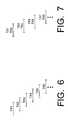
- the conductorsare processed in overlapping periods of time that are shifted relative to one another.
- An exampleis shown in FIG. 6 .
- the processing time TX 1 of conductor X 1overlaps with the time TX 2 for conductor X 2 , but the time TX 2 starts later than TX 1 .
- TX 3overlaps with TX 2 , but starts later than TX 2 , and so on.
- the conductors X 1 , X 2are processed simultaneously (like in FIG. 4 ).
- the conductors X 3 and X 4are also processed simultaneously.
- the time “TX 3 , TX 4 ”overlaps with “TX 1 , TX 2 ” but starts later than “TX 1 , TX 2 ”.
- more than two conductorsare processed simultaneously, yet for at least two conductors their processing times overlap but are shifted relative to each other.
- the processing time overlapallows the conductors to be processed faster than in the sequential systems.
- the response time to a movement of a finger or a stylusis improved, and/or more time is left for digital and other processing.
- less circuitryis required than in the simultaneous processing systems.
- less analog circuitryis needed, relaxing the analog circuit design and process trimming requirements.
- the power driving requirementsare reduced compared to the simultaneous processing systems.
- FIG. 8shows a voltage of a conductor Xn as a function of time.
- the conductor processingincludes a discharge phase Dn, a charging phase Cn, and a sensing phase Sn. In phase Dn, the conductor is discharged to ground.
- phase Cna predetermined amount of charge is injected into the conductor.
- phase Snthe charge on the conductor is sampled with a sample and hold circuit (not shown).
- the phases Dn, Cn, Snare of equal duration.
- FIG. 9shows the relative timing of the three phases for the conductors X 1 , X 2 , X 3 .
- the processing of a conductoris delayed by one phase duration relative to the previous conductor, so that D 2 coincides with C 1 , D 3 with C 2 and S 1 , and so on. More generally, the phases Sn, Cn+1, Dn+2 coincide.
- phase period Tat most one conductor is in any given phase (discharge, charge, or sense), so the circuitry for each phase can be shared by different conductors. For example, only one sample and hold circuit is needed. In addition, the current drive requirements for the charging and discharging circuitry (phases Cn and Dn) can be reduced since at most one conductor is charged and at most one conductor is discharged at any time.
- each phase period Tone conductor is in the sensing phase S, one conductor is in the charging phase C, and the remaining conductors are in the discharge phase.
- the grounded conductorsreduce the amount of noise injected into the adjacent conductors.
- each phase period Tone conductor is in the sensing phase, multiple conductors are in the charging phase, and multiple conductors are in the discharge phase. More generally, any number of conductors can be in the sensing stage, any number of conductors can be in the charging phase, and any number of conductors can be in the discharge phase in one phase period T. Multiple copies of the sensing, charging and discharge circuits can be provided.
- the inventionis not limited to the embodiments described above.
- the inventionis not limited to embodiments in which the discharging, charging or sensing circuitry is shared among different conductors, or to embodiments with low current driving requirements.
- the phases Dn, Cn, Sndo not have to be of equal duration.
- different phasesmay be overlap or even occur at the same time for a given conductor.
- the charging and sensing of a conductorcan be done at the same time.
- the phasescan be different from those in FIG. 8 .
- the inventionis applicable to systems in which the conductors are coupled to the driving (charging) and sensing lines capacitively. See U.S. Pat. No. 4,733,222 issued Mar. 22, 1988 to Evans and incorporated herein by reference. Other embodiments and variations are within the scope of the invention, as described below and defined by the appended claims.
- FIG. 1illustrates a prior art touch sensitive system.
- FIG. 2is a block diagram of a prior art sensing and processing circuit.
- FIG. 3is a timing diagram for the circuit of FIG. 2 .
- FIG. 4is a block diagram of another prior art sensing and processing circuit.
- FIG. 5is a timing diagram for the circuit of FIG. 4 .
- FIGS. 6 and 7are timing diagrams illustrating some embodiments of the present invention.
- FIG. 8is a conductor voltage plot in one embodiment of the present invention.
- FIG. 9is a timing diagram for the embodiment of FIG. 8 .
- FIG. 10is a block diagram of sensing and processing circuitry according to some embodiments of the present invention.
- FIG. 11is a block and circuit diagram of one implementation of a portion of the circuitry of FIG. 10 .
- FIG. 12is a timing diagram obtained in one embodiment of the present invention.
- FIGS. 13 and 14are circuit diagrams for one implementation of a portion of the circuitry of FIG. 10 .
- FIG. 15is a block and circuit diagram according to an embodiment of the present invention.
- FIG. 16is a top view of a prior art touch sensitive pad suitable for use with some embodiments of the present invention.
- FIG. 17is a cross sectional view of the pad of FIG. 16 .
- FIG. 10illustrates an example touch sensitive system that implements the timing of FIGS. 8 and 9 .
- Capacitors 1010schematically represent the capacitances of the respective conductors X 1 . . . XN. The capacitors are not actually present in the circuit.
- the total capacitance of a conductor, as represented by a capacitor 1010includes a base capacitance (e.g. the capacitance associated with the position of the conductors on a touch pad substrate, which can be a printed circuit board) and a capacitance due to a proximity of a conductive object such as a finger or a stylus.
- a base capacitancee.g. the capacitance associated with the position of the conductors on a touch pad substrate, which can be a printed circuit board
- a capacitance due to a proximity of a conductive objectsuch as a finger or a stylus.
- the conductorscan be arranged as in FIG. 1 or in any other suitable fashion.
- a radial arrangementis possible as in the aforementioned U.S. Pat. No. 4,736,191, incorporated herein by reference.
- the conductorscan be arranged on a flat or curved surface or in any suitable way.
- the N conductorsare connected to inputs of N:3 multiplexer 1020 .
- multiplexer 1020selects three conductors Xn, Xn+1, Xn+2 for the discharge, charging, and sensing phases.
- the outputs of MUX 1020are connected to inputs of respective driving and sensing circuits 1030 . 1 , 1030 . 2 , 1030 . 3 . Each of these circuits performs the discharging, charging, and sensing operations for one selected conductor.
- circuits 1030are connected to the respective inputs of 3:1 multiplexer 1040 .
- Multiplexer 1040selects a circuit 1030 when the circuit is in the sensing phase.
- the output of multiplexer 1040is connected to a sample and hold circuit 1050 .
- the output of sample and hold circuit 1050is connected to the input of analog to digital converter 1060 .
- the output of ADC 1060is connected to a digital processing circuit 1070 which may perform filtering, calibration, and other processing.
- ADC 1060 and circuit 1070are shown for illustration. The invention is not limited to any digital processing functions or their sequence, or to any function being implemented with digital circuitry. For example, the filtering can be performed before the A/D conversion, or can be omitted.
- the circuits 1020 , 1030 , 1040 , 1050 , 1060are controlled by a time division multiplexing (TDM) control circuit 1080 .
- Digital processing circuit 1070is controlled by a timing control circuit 1090 .
- Circuit 1090provides a Start signal to circuit 1080 to start conductor processing.
- Circuit 1080asserts a Ready signal Rdy to circuit 1090 near the end of each sensing phase to indicate that data sampled for one conductor are available for digital processing.
- This control schemeis provided for illustration and is not limiting.
- Circuits 1030 . 1 , 1030 . 2 , 1030 . 3are identical.
- FIG. 11illustrates one such circuit.
- Switch 1110 in TDM multiplexer 1020when closed, establishes a conductive path between a conductor Xn and an input terminal IN (terminal 1114 ) of circuit 1030 .
- Switch 1120 in 3:1 MUX 1040establishes a conductive path between the output terminal OUT of circuit 1030 and the input of S/H circuit 1050 .
- S/H circuit 1050is shown as a conventional circuit consisting essentially of (i) a pass gate 1122 connected between the output of multiplexer 1040 and the output 1124 of S/H 1050 , and (ii) a capacitor 1126 connected between the terminal 1124 and ground.
- Terminal 1124is connected to the input of A/D converter 1060 .
- Other types of S/H circuitsare also possible.
- Terminal IN of circuit 1030is connected to current source 1130 through switch 1140 , to ground through switch 1150 , and to terminal OUT through switch 1160 .
- Each switchwhen closed, establishes a conductive path between its terminals.
- the switchescan be implemented as transistors, pass gates, or in any other fashion, known or to be invented.
- the switches and the pass gate 1122are controlled by TDM control 1080 .
- switch 1150is closed and the switches 1140 , 1160 are open.
- Conductor Xnis discharged to ground.
- switch 1140is closed and switches 1150 , 1160 are open for a predetermined interval of time.
- Current source 1130sources a predetermined current, injecting a predetermined charge Q into the conductor Xn.
- switch 1160is closed and the switches 1140 , 1150 are open.
- the charge Qbecomes shared with the output OUT.
- the switch 1120is closed, and some of the charge is passed to the input of S/H circuit 1050 .
- Switch 1110is closed in all of the three phases Dn, Cn, Sn.
- Switch 1160can be omitted. Terminal IN can be connected directly to multiplexer 1040 .
- the conductor scanning operationbegins in response to a pulse of the signal Start provided by timing control 1090 .
- a pulseindicates the time when the corresponding conductor is selected by TDM multiplexer 1020 .
- TDM multiplexer 1020At first, only conductor X 1 is selected. Then X 2 is selected before deselection of X 1 , and X 3 is selected before deselection of X 1 and X 2 .
- a pulseindicates the time when the circuit 1030 . 1 is in the discharge phase, the circuit 1030 . 2 is in the charging phase, and the circuit 1030 . 3 is in the sensing phase.
- a pulse in the “1C, 2S, 3D” diagramindicates the time when the circuit 1030 . 1 is in the charging phase, the circuit 1030 . 2 is in the sensing phase, and the circuit 1030 . 3 is in the discharge phase.
- a pulse in the “1S, 2D, 3C” diagramindicates the time when the circuit 1030 . 1 is in the sensing phase, the circuit 1030 . 2 is in the discharge phase, and the circuit 1030 . 3 is in the charging phase.
- the duration of each phaseis 2.5-20.0 ⁇ s. Other durations are also possible.
- signal Rdyis asserted by TDM control 1080 to indicate valid digital data on the output of ADC 1060 .
- the datacan be stored in a register (not shown) in circuit 1070 , and/or processed in a suitable way.
- the Frame signalis asserted by TDM control 1080 to timing control 1090 when the last conductor is being scanned.
- a new scanning cyclecan be initiated by asserting Start.
- This sequenceis exemplary and not limiting. For example, scanning of all of the conductors can be performed multiple times without assertion of a Start signal (“free running mode”). The scanning can be performed with wrap around or in any other order.
- FIG. 13illustrates a circuit diagram for one implementation of circuit 1030 of FIG. 11 .
- Switches 1140 , 1150 , 1160are pass gates.
- a pass gateis a pair of an NMOS transistor and a PMOS transistor connected in parallel between the switch terminals.
- Current source 1130includes PMOS transistors 1310 , 1320 , 1330 , 1340 in current mirror configuration.
- the sources of transistors 1310 , 1330are connected to a positive voltage supply VDD.
- the gates of the two transistorsare connected to each other and to the drain of transistor 1310 .
- the drain of transistor 1310is connected to the source of transistor 1320 .
- the gate of transistor 1320is connected to its drain and to the gate of transistor 1340 .
- the drain of transistor 1320is connected to output terminal 1350 of a current source 1404 ( FIG. 14 ) that sinks a constant current Ibias from terminal 1350 .
- the circuit of FIG. 13is exemplary and not limiting.
- the drain of transistor 1330is connected to the source of transistor 1340 .
- the drain of transistor 1340is connected to switch 1140 .
- Current source 1404includes PMOS transistors 1410 , 1420 , 1430 , 1440 in current mirror configuration.
- the sources of transistors 1410 , 1430are connected to VDD.
- the gates of the two transistorsare connected to each other and to the drain of transistor 1410 .
- the drain of transistor 1410is connected to the source of transistor 1420 .
- the gate of transistor 1420is connected to its drain 1450 and to the gate of transistor 1440 .
- the source of transistor 1440is connected to the drain of transistor 1430 .
- the circuit of FIG. 14is exemplary and not limiting.
- the drain node 1450 of transistor 1420is connected to the drain of NMOS transistor 1460 .
- the gate of transistor 1460is connected to the output of operational amplifier 1464 .
- the positive input terminal of amplifier 1464receives a positive reference voltage Vref.
- the negative input terminal of amplifier 1464is connected to the source of transistor 1460 and to one terminal of resistor 1468 .
- the other terminal of resistor 1468is connected to ground.
- the current through transistor 1410is mirrored to the drain of transistor 1440 .
- the drain of transistor 1440is connected to the drain and the gate of NMOS transistor 1470 .
- the source of transistor 1470is connected to the drain and the gate of NMOS transistor 1474 .
- the source of transistor 1474is connected to ground.
- the gate of transistor 1474is connected to the gate of NMOS transistor 1480 whose source is connected to ground.
- the drain of transistor 1480is connected to the source of NMOS transistor 1490 .
- the gate of transistor 1490is connected to the gate of transistor 1470 .
- the drain of transistor 1490is connected to terminal 1350 .
- current source 1404is shared by circuits 1030 . 1 , 1030 . 2 , 1030 . 3 .
- Current source 1130 , and other circuitry,can also be shared as shown in FIG. 15 .
- Multiplexers 1020 , 1040are replaced with a cross connect circuit 1510 having N inputs connected to the respective conductors X 1 , . . . XN.
- Circuit 1510has three outputs connected, respectively, to the output of current source 1130 , a ground terminal, and one terminal of switch 1160 .
- the other terminal of switch 1160is connected to the input of S/H circuit 1050 .
- the cross connect 1510simultaneously selects three conductors and connects one of the conductors to ground for the discharge phase, one of the conductors to current source 1130 for the charging phase, and one of the conductors to switch 1160 for the sensing stage.
- switch 1160is omitted, and the corresponding output of cross connect 1510 is connected directly to the input of S/H 1050 .
- the driving and sensing circuits 1030are identical to the charge integrators 410 ( FIG. 4 ) described in the aforementioned U.S. Pat. No. 5,914,465. These circuits operate as follows. First the conductor connected to such a circuit 1030 is shorted to a voltage VDD. Then the circuit 1030 discharges the conductor with a constant current for a fixed period of time. The resulting conductor voltage appears on a plate of a capacitor. Then the conductor is shorted to ground, and then charged with a constant current for a fixed period of time. The resulting conductor voltage appears on a plate of another capacitor. The voltages on the two plates of the two capacitors are averaged. The averaged voltage is passed to S/H 1050 .
- each circuit 1030operates like the processing circuitry of FIG. 2 (measuring the time that it takes to change the conductor voltage from one value, e.g. ground, to another value). In some embodiments, circuits 1030 sense the conductor states by sensing a current through the conductor or some other physical parameter. Other variations are possible, known or to be invented.
- FIGS. 16-17illustrated an exemplary prior art touch pad 110 used in some embodiments of the invention.
- FIG. 16is a top view showing the conductors 120 X and also showing diamond shaped pads 120 Y-P which are part of conductors 120 Y.
- FIG. 17is a cross section along the line XVII—XVII in FIG. 16 .
- Conductors 120 X and pads 120 Y-Pare conductive traces (e.g. copper) formed on an insulating printed circuit board (PCB) 1710 .
- Conductors 120 Yalso include the conductive traces 120 Y-L on the bottom surface of PCB 1710 .
- Each trace 120 Y-Lis connected to one row of pads 120 Y-P by metal plugs 120 Y-M formed in through holes in PCB 1710 .
- Dielectric 1720is formed over the traces 120 X, 120 Y-P. Dielectric 1720 separates these traces from a finger or stylus 130 . Dielectric 1730 formed underneath PCB 1710 over the traces 120 Y-L.
- touch pad and touch surface structures and featuresare described in U.S. Pat. Nos. 5,914,465; 4,736,191 and 4,639,720, which are incorporated herein by reference.
- Other touch pad structuresincluding three-dimensional structures, one-dimensional structures, and other structures, known or to be invented, can also be suitable.
- the inventionis not limited to sensing a human finger or a stylus, but extends to sensing other types of objects.
- the inventionis not-limited to the circuits and structures described above, but is defined by the appended claims.
Landscapes
- Engineering & Computer Science (AREA)
- General Engineering & Computer Science (AREA)
- Theoretical Computer Science (AREA)
- Human Computer Interaction (AREA)
- Physics & Mathematics (AREA)
- General Physics & Mathematics (AREA)
- Measurement Of Resistance Or Impedance (AREA)
- Electronic Switches (AREA)
- Investigating Or Analyzing Materials By The Use Of Electric Means (AREA)
- Measurement Of Length, Angles, Or The Like Using Electric Or Magnetic Means (AREA)
- Position Input By Displaying (AREA)
- Switches That Are Operated By Magnetic Or Electric Fields (AREA)
- Push-Button Switches (AREA)
Abstract
Description
Claims (34)
Priority Applications (4)
| Application Number | Priority Date | Filing Date | Title |
|---|---|---|---|
| US10/190,251US6891531B2 (en) | 2002-07-05 | 2002-07-05 | Sensing an object with a plurality of conductors |
| TW091121057ATWI225621B (en) | 2002-07-05 | 2002-09-13 | Sensing an object with a plurality of conductors |
| CNB021434034ACN1221883C (en) | 2002-07-05 | 2002-09-24 | Method and device for detecting object with multiple conductors |
| JP2002332959AJP2004038919A (en) | 2002-07-05 | 2002-11-15 | Method for detecting object by using a plurality of electric conductors |
Applications Claiming Priority (1)
| Application Number | Priority Date | Filing Date | Title |
|---|---|---|---|
| US10/190,251US6891531B2 (en) | 2002-07-05 | 2002-07-05 | Sensing an object with a plurality of conductors |
Publications (2)
| Publication Number | Publication Date |
|---|---|
| US20040003949A1 US20040003949A1 (en) | 2004-01-08 |
| US6891531B2true US6891531B2 (en) | 2005-05-10 |
Family
ID=29780133
Family Applications (1)
| Application Number | Title | Priority Date | Filing Date |
|---|---|---|---|
| US10/190,251Expired - LifetimeUS6891531B2 (en) | 2002-07-05 | 2002-07-05 | Sensing an object with a plurality of conductors |
Country Status (4)
| Country | Link |
|---|---|
| US (1) | US6891531B2 (en) |
| JP (1) | JP2004038919A (en) |
| CN (1) | CN1221883C (en) |
| TW (1) | TWI225621B (en) |
Cited By (20)
| Publication number | Priority date | Publication date | Assignee | Title |
|---|---|---|---|---|
| US20060114241A1 (en)* | 2004-11-29 | 2006-06-01 | Holtek Semiconductor Inc. | Identification method for touch control device |
| US20070268265A1 (en)* | 2006-05-18 | 2007-11-22 | Cypress Semiconductor Corporation | Two-pin buttons |
| US20080179112A1 (en)* | 2007-01-30 | 2008-07-31 | Zheng Qin | Setting a discharge rate and a charge rate of a relaxation oscillator circuit |
| US20100026639A1 (en)* | 2008-08-04 | 2010-02-04 | Samsung Electronics Co., Ltd. | Liquid crystal display and touch sensing method thereof |
| US20110181549A1 (en)* | 2007-01-03 | 2011-07-28 | Steve Porter Hotelling | Double-sided touch-sensitive panel with shield and drive combined layer |
| US8040142B1 (en) | 2006-03-31 | 2011-10-18 | Cypress Semiconductor Corporation | Touch detection techniques for capacitive touch sense systems |
| US8321174B1 (en) | 2008-09-26 | 2012-11-27 | Cypress Semiconductor Corporation | System and method to measure capacitance of capacitive sensor array |
| US8358142B2 (en) | 2008-02-27 | 2013-01-22 | Cypress Semiconductor Corporation | Methods and circuits for measuring mutual and self capacitance |
| US8525798B2 (en) | 2008-01-28 | 2013-09-03 | Cypress Semiconductor Corporation | Touch sensing |
| US8536902B1 (en) | 2007-07-03 | 2013-09-17 | Cypress Semiconductor Corporation | Capacitance to frequency converter |
| US8547114B2 (en) | 2006-11-14 | 2013-10-01 | Cypress Semiconductor Corporation | Capacitance to code converter with sigma-delta modulator |
| US8570053B1 (en) | 2007-07-03 | 2013-10-29 | Cypress Semiconductor Corporation | Capacitive field sensor with sigma-delta modulator |
| US8570052B1 (en) | 2008-02-27 | 2013-10-29 | Cypress Semiconductor Corporation | Methods and circuits for measuring mutual and self capacitance |
| US8928618B2 (en) | 2004-05-06 | 2015-01-06 | Apple Inc. | Multipoint touchscreen |
| USRE45559E1 (en) | 1997-10-28 | 2015-06-09 | Apple Inc. | Portable computers |
| US9104273B1 (en) | 2008-02-29 | 2015-08-11 | Cypress Semiconductor Corporation | Multi-touch sensing method |
| US9417728B2 (en) | 2009-07-28 | 2016-08-16 | Parade Technologies, Ltd. | Predictive touch surface scanning |
| US9500686B1 (en) | 2007-06-29 | 2016-11-22 | Cypress Semiconductor Corporation | Capacitance measurement system and methods |
| US10175832B2 (en) | 2011-12-22 | 2019-01-08 | Quickstep Technologies Llc | Switched-electrode capacitive-measurement device for touch-sensitive and contactless interfaces |
| US10503328B2 (en) | 2011-06-16 | 2019-12-10 | Quickstep Technologies Llc | Device and method for generating an electrical power supply in an electronic system with a variable reference potential |
Families Citing this family (31)
| Publication number | Priority date | Publication date | Assignee | Title |
|---|---|---|---|---|
| JP4528150B2 (en)* | 2005-02-14 | 2010-08-18 | 京セラ株式会社 | Concavity and convexity pattern detection apparatus and method |
| CN102841713A (en)* | 2005-09-15 | 2012-12-26 | 苹果公司 | System and method for processing raw data of track pad device |
| TWI313431B (en)* | 2006-04-14 | 2009-08-11 | Ritdisplay Corporatio | Transparent touch panel |
| CN104965621B (en) | 2006-06-09 | 2018-06-12 | 苹果公司 | Touch screen LCD and its operating method |
| CN102981678B (en) | 2006-06-09 | 2015-07-22 | 苹果公司 | Touch screen liquid crystal display |
| US9507465B2 (en)* | 2006-07-25 | 2016-11-29 | Cypress Semiconductor Corporation | Technique for increasing the sensitivity of capacitive sensor arrays |
| US9710095B2 (en) | 2007-01-05 | 2017-07-18 | Apple Inc. | Touch screen stack-ups |
| JP4945345B2 (en)* | 2007-07-03 | 2012-06-06 | 株式会社 日立ディスプレイズ | Display device with touch panel |
| JP4932667B2 (en)* | 2007-10-17 | 2012-05-16 | 株式会社 日立ディスプレイズ | Screen input type image display system |
| US8072356B2 (en)* | 2007-12-13 | 2011-12-06 | Kyocera Corporation | Capacitive sensing user interfaces and implementation thereof |
| TWI361996B (en)* | 2008-03-21 | 2012-04-11 | Elan Microelectronics Corp | Touch panel device |
| JP5191769B2 (en)* | 2008-03-27 | 2013-05-08 | ルネサスエレクトロニクス株式会社 | Capacity detection apparatus and method |
| JP5229887B2 (en)* | 2008-08-06 | 2013-07-03 | 株式会社ワコム | Position detection device |
| CN101666830B (en)* | 2008-09-01 | 2013-01-02 | 瑞鼎科技股份有限公司 | Capacitance value measuring circuit and electronic device using it |
| JP5067763B2 (en)* | 2008-10-08 | 2012-11-07 | 株式会社ジャパンディスプレイウェスト | Contact detection device, display device, and contact detection method |
| TW201017501A (en)* | 2008-10-31 | 2010-05-01 | Elan Microelectronics Corp | The control circuit, method, and applications of capacitive touch panel |
| JP5486854B2 (en)* | 2009-06-29 | 2014-05-07 | 株式会社ジャパンディスプレイ | Information input device, display device |
| JP5361579B2 (en)* | 2009-07-09 | 2013-12-04 | 信越ポリマー株式会社 | Sensor panel for large display and manufacturing method thereof |
| CN102004590B (en)* | 2009-09-01 | 2015-03-04 | 义隆电子股份有限公司 | Front-end signal detector and method for improving anti-noise ability of capacitive touch panel |
| JP5667824B2 (en) | 2010-09-24 | 2015-02-12 | 株式会社ジャパンディスプレイ | Touch detection device and driving method thereof, display device with touch detection function, and electronic device |
| CN101976147B (en) | 2010-09-30 | 2013-03-27 | 江苏惠通集团有限责任公司 | Touch recognition method, touch key structure and touch device |
| US8804056B2 (en) | 2010-12-22 | 2014-08-12 | Apple Inc. | Integrated touch screens |
| TWI472971B (en)* | 2012-02-20 | 2015-02-11 | Innocom Tech Shenzhen Co Ltd | An electronic device and sensing method |
| TWI486847B (en)* | 2012-03-15 | 2015-06-01 | 義隆電子股份有限公司 | Scan method of touch panel to increase frame rate and touch panel using the same |
| JP5231668B2 (en)* | 2012-03-29 | 2013-07-10 | 株式会社ジャパンディスプレイイースト | Capacitive coupling type touch panel |
| JP5509473B2 (en)* | 2012-04-27 | 2014-06-04 | 株式会社ジャパンディスプレイ | Touch panel |
| JP5236099B2 (en)* | 2012-05-09 | 2013-07-17 | 株式会社ジャパンディスプレイイースト | Touch panel |
| US9971463B2 (en)* | 2015-09-29 | 2018-05-15 | Synaptics Incorporated | Row-based sensing on matrix pad sensors |
| US10705647B2 (en)* | 2016-12-30 | 2020-07-07 | Lg Display Co., Ltd. | Touch display device capable of selectively changing characteristic of touch driving signal |
| JP6480623B2 (en)* | 2018-04-12 | 2019-03-13 | 株式会社ジャパンディスプレイ | Capacitive coupling touch panel manufacturing method |
| CN112965641B (en)* | 2021-05-18 | 2021-09-10 | 深圳曦华科技有限公司 | Capacitance detection circuit, related method, module, device and equipment |
Citations (22)
| Publication number | Priority date | Publication date | Assignee | Title |
|---|---|---|---|---|
| US3497617A (en) | 1966-09-07 | 1970-02-24 | Marconi Co Ltd | Electrical position resolver arrangements |
| US3921166A (en) | 1972-09-15 | 1975-11-18 | Raytheon Co | Capacitance matrix keyboard |
| US4103252A (en) | 1976-11-26 | 1978-07-25 | Xerox Corporation | Capacitive touch-activated transducer system including a plurality of oscillators |
| JPS59121484A (en)* | 1982-12-27 | 1984-07-13 | Casio Comput Co Ltd | Coordinate input device |
| US4550221A (en) | 1983-10-07 | 1985-10-29 | Scott Mabusth | Touch sensitive control device |
| US4639720A (en) | 1981-01-12 | 1987-01-27 | Harris Corporation | Electronic sketch pad |
| US4680430A (en) | 1984-02-29 | 1987-07-14 | Fujitsu Limited | Coordinate detecting apparatus |
| US4686332A (en) | 1986-06-26 | 1987-08-11 | International Business Machines Corporation | Combined finger touch and stylus detection system for use on the viewing surface of a visual display device |
| US4733222A (en) | 1983-12-27 | 1988-03-22 | Integrated Touch Arrays, Inc. | Capacitance-variation-sensitive touch sensing array system |
| US4736191A (en) | 1985-08-02 | 1988-04-05 | Karl E. Matzke | Touch activated control method and apparatus |
| WO1991003039A1 (en) | 1989-08-16 | 1991-03-07 | Gerpheide George E | Methods and apparatus for data input |
| US5016008A (en) | 1987-05-25 | 1991-05-14 | Sextant Avionique | Device for detecting the position of a control member on a touch-sensitive pad |
| US5149919A (en) | 1990-10-31 | 1992-09-22 | International Business Machines Corporation | Stylus sensing system |
| US5349303A (en) | 1993-07-02 | 1994-09-20 | Cirque Corporation | Electrical charge transfer apparatus |
| US5374787A (en) | 1992-06-08 | 1994-12-20 | Synaptics, Inc. | Object position detector |
| US5565658A (en) | 1992-07-13 | 1996-10-15 | Cirque Corporation | Capacitance-based proximity with interference rejection apparatus and methods |
| US5914465A (en) | 1992-06-08 | 1999-06-22 | Synaptics, Inc. | Object position detector |
| US5914708A (en) | 1996-04-04 | 1999-06-22 | Cirque Corporation | Computer input stylus method and apparatus |
| US6222528B1 (en) | 1997-03-07 | 2001-04-24 | Cirque Corporation | Method and apparatus for data input |
| US6239788B1 (en)* | 1997-08-08 | 2001-05-29 | Sharp Kabushiki Kaisha | Coordinate input device and display-integrated type coordinate input device capable of directly detecting electrostatic coupling capacitance with high accuracy |
| US6262717B1 (en) | 1998-07-02 | 2001-07-17 | Cirque Corporation | Kiosk touch pad |
| US6452514B1 (en)* | 1999-01-26 | 2002-09-17 | Harald Philipp | Capacitive sensor and array |
- 2002
- 2002-07-05USUS10/190,251patent/US6891531B2/ennot_activeExpired - Lifetime
- 2002-09-13TWTW091121057Apatent/TWI225621B/ennot_activeIP Right Cessation
- 2002-09-24CNCNB021434034Apatent/CN1221883C/ennot_activeExpired - Fee Related
- 2002-11-15JPJP2002332959Apatent/JP2004038919A/enactivePending
Patent Citations (23)
| Publication number | Priority date | Publication date | Assignee | Title |
|---|---|---|---|---|
| US3497617A (en) | 1966-09-07 | 1970-02-24 | Marconi Co Ltd | Electrical position resolver arrangements |
| US3921166A (en) | 1972-09-15 | 1975-11-18 | Raytheon Co | Capacitance matrix keyboard |
| US4103252A (en) | 1976-11-26 | 1978-07-25 | Xerox Corporation | Capacitive touch-activated transducer system including a plurality of oscillators |
| US4639720A (en) | 1981-01-12 | 1987-01-27 | Harris Corporation | Electronic sketch pad |
| JPS59121484A (en)* | 1982-12-27 | 1984-07-13 | Casio Comput Co Ltd | Coordinate input device |
| US4550221A (en) | 1983-10-07 | 1985-10-29 | Scott Mabusth | Touch sensitive control device |
| US4733222A (en) | 1983-12-27 | 1988-03-22 | Integrated Touch Arrays, Inc. | Capacitance-variation-sensitive touch sensing array system |
| US4680430A (en) | 1984-02-29 | 1987-07-14 | Fujitsu Limited | Coordinate detecting apparatus |
| US4736191A (en) | 1985-08-02 | 1988-04-05 | Karl E. Matzke | Touch activated control method and apparatus |
| US4686332A (en) | 1986-06-26 | 1987-08-11 | International Business Machines Corporation | Combined finger touch and stylus detection system for use on the viewing surface of a visual display device |
| US5016008A (en) | 1987-05-25 | 1991-05-14 | Sextant Avionique | Device for detecting the position of a control member on a touch-sensitive pad |
| WO1991003039A1 (en) | 1989-08-16 | 1991-03-07 | Gerpheide George E | Methods and apparatus for data input |
| US5149919A (en) | 1990-10-31 | 1992-09-22 | International Business Machines Corporation | Stylus sensing system |
| US5374787A (en) | 1992-06-08 | 1994-12-20 | Synaptics, Inc. | Object position detector |
| US5495077A (en) | 1992-06-08 | 1996-02-27 | Synaptics, Inc. | Object position and proximity detector |
| US5914465A (en) | 1992-06-08 | 1999-06-22 | Synaptics, Inc. | Object position detector |
| US5565658A (en) | 1992-07-13 | 1996-10-15 | Cirque Corporation | Capacitance-based proximity with interference rejection apparatus and methods |
| US5349303A (en) | 1993-07-02 | 1994-09-20 | Cirque Corporation | Electrical charge transfer apparatus |
| US5914708A (en) | 1996-04-04 | 1999-06-22 | Cirque Corporation | Computer input stylus method and apparatus |
| US6222528B1 (en) | 1997-03-07 | 2001-04-24 | Cirque Corporation | Method and apparatus for data input |
| US6239788B1 (en)* | 1997-08-08 | 2001-05-29 | Sharp Kabushiki Kaisha | Coordinate input device and display-integrated type coordinate input device capable of directly detecting electrostatic coupling capacitance with high accuracy |
| US6262717B1 (en) | 1998-07-02 | 2001-07-17 | Cirque Corporation | Kiosk touch pad |
| US6452514B1 (en)* | 1999-01-26 | 2002-09-17 | Harald Philipp | Capacitive sensor and array |
Cited By (43)
| Publication number | Priority date | Publication date | Assignee | Title |
|---|---|---|---|---|
| USRE45559E1 (en) | 1997-10-28 | 2015-06-09 | Apple Inc. | Portable computers |
| USRE46548E1 (en) | 1997-10-28 | 2017-09-12 | Apple Inc. | Portable computers |
| US8928618B2 (en) | 2004-05-06 | 2015-01-06 | Apple Inc. | Multipoint touchscreen |
| US20060114241A1 (en)* | 2004-11-29 | 2006-06-01 | Holtek Semiconductor Inc. | Identification method for touch control device |
| US8248084B2 (en) | 2006-03-31 | 2012-08-21 | Cypress Semiconductor Corporation | Touch detection techniques for capacitive touch sense systems |
| US9494627B1 (en) | 2006-03-31 | 2016-11-15 | Monterey Research, Llc | Touch detection techniques for capacitive touch sense systems |
| US8040142B1 (en) | 2006-03-31 | 2011-10-18 | Cypress Semiconductor Corporation | Touch detection techniques for capacitive touch sense systems |
| US8004497B2 (en) | 2006-05-18 | 2011-08-23 | Cypress Semiconductor Corporation | Two-pin buttons |
| US8519973B1 (en) | 2006-05-18 | 2013-08-27 | Cypress Semiconductor Corporation | Apparatus and methods for detecting a conductive object at a location |
| US20070268265A1 (en)* | 2006-05-18 | 2007-11-22 | Cypress Semiconductor Corporation | Two-pin buttons |
| US10209833B1 (en) | 2006-05-18 | 2019-02-19 | Creator Technology B.V. | Apparatus and methods for detecting a conductive object at a location |
| US8547114B2 (en) | 2006-11-14 | 2013-10-01 | Cypress Semiconductor Corporation | Capacitance to code converter with sigma-delta modulator |
| US9154160B2 (en) | 2006-11-14 | 2015-10-06 | Cypress Semiconductor Corporation | Capacitance to code converter with sigma-delta modulator |
| US9166621B2 (en) | 2006-11-14 | 2015-10-20 | Cypress Semiconductor Corporation | Capacitance to code converter with sigma-delta modulator |
| US9836160B2 (en) | 2007-01-03 | 2017-12-05 | Apple Inc. | Double-sided touch-sensitive panel with shield and drive combined layer |
| US20110181549A1 (en)* | 2007-01-03 | 2011-07-28 | Steve Porter Hotelling | Double-sided touch-sensitive panel with shield and drive combined layer |
| US11112904B2 (en) | 2007-01-03 | 2021-09-07 | Apple Inc. | Double-sided touch-sensitive panel with shield and drive combined layer |
| US9465502B2 (en) | 2007-01-03 | 2016-10-11 | Apple Inc. | Double-sided touch-sensitive panel with shield and drive combined layer |
| US8884890B2 (en) | 2007-01-03 | 2014-11-11 | Apple Inc. | Double-sided touch-sensitive panel with shield and drive combined layer |
| US10474287B2 (en) | 2007-01-03 | 2019-11-12 | Apple Inc. | Double-sided touch-sensitive panel with shield and drive combined layer |
| US9075491B2 (en) | 2007-01-03 | 2015-07-07 | Apple Inc. | Double-sided touch-sensitive panel with shield and drive combined layer |
| US8058937B2 (en) | 2007-01-30 | 2011-11-15 | Cypress Semiconductor Corporation | Setting a discharge rate and a charge rate of a relaxation oscillator circuit |
| US20080179112A1 (en)* | 2007-01-30 | 2008-07-31 | Zheng Qin | Setting a discharge rate and a charge rate of a relaxation oscillator circuit |
| US9500686B1 (en) | 2007-06-29 | 2016-11-22 | Cypress Semiconductor Corporation | Capacitance measurement system and methods |
| US8570053B1 (en) | 2007-07-03 | 2013-10-29 | Cypress Semiconductor Corporation | Capacitive field sensor with sigma-delta modulator |
| US11549975B2 (en) | 2007-07-03 | 2023-01-10 | Cypress Semiconductor Corporation | Capacitive field sensor with sigma-delta modulator |
| US10025441B2 (en) | 2007-07-03 | 2018-07-17 | Cypress Semiconductor Corporation | Capacitive field sensor with sigma-delta modulator |
| US8536902B1 (en) | 2007-07-03 | 2013-09-17 | Cypress Semiconductor Corporation | Capacitance to frequency converter |
| US8525798B2 (en) | 2008-01-28 | 2013-09-03 | Cypress Semiconductor Corporation | Touch sensing |
| US9760192B2 (en) | 2008-01-28 | 2017-09-12 | Cypress Semiconductor Corporation | Touch sensing |
| US8570052B1 (en) | 2008-02-27 | 2013-10-29 | Cypress Semiconductor Corporation | Methods and circuits for measuring mutual and self capacitance |
| US9494628B1 (en) | 2008-02-27 | 2016-11-15 | Parade Technologies, Ltd. | Methods and circuits for measuring mutual and self capacitance |
| US8692563B1 (en) | 2008-02-27 | 2014-04-08 | Cypress Semiconductor Corporation | Methods and circuits for measuring mutual and self capacitance |
| US9423427B2 (en) | 2008-02-27 | 2016-08-23 | Parade Technologies, Ltd. | Methods and circuits for measuring mutual and self capacitance |
| US8358142B2 (en) | 2008-02-27 | 2013-01-22 | Cypress Semiconductor Corporation | Methods and circuits for measuring mutual and self capacitance |
| US9104273B1 (en) | 2008-02-29 | 2015-08-11 | Cypress Semiconductor Corporation | Multi-touch sensing method |
| US20100026639A1 (en)* | 2008-08-04 | 2010-02-04 | Samsung Electronics Co., Ltd. | Liquid crystal display and touch sensing method thereof |
| US10386969B1 (en) | 2008-09-26 | 2019-08-20 | Cypress Semiconductor Corporation | System and method to measure capacitance of capacitive sensor array |
| US8321174B1 (en) | 2008-09-26 | 2012-11-27 | Cypress Semiconductor Corporation | System and method to measure capacitance of capacitive sensor array |
| US11029795B2 (en) | 2008-09-26 | 2021-06-08 | Cypress Semiconductor Corporation | System and method to measure capacitance of capacitive sensor array |
| US9417728B2 (en) | 2009-07-28 | 2016-08-16 | Parade Technologies, Ltd. | Predictive touch surface scanning |
| US10503328B2 (en) | 2011-06-16 | 2019-12-10 | Quickstep Technologies Llc | Device and method for generating an electrical power supply in an electronic system with a variable reference potential |
| US10175832B2 (en) | 2011-12-22 | 2019-01-08 | Quickstep Technologies Llc | Switched-electrode capacitive-measurement device for touch-sensitive and contactless interfaces |
Also Published As
| Publication number | Publication date |
|---|---|
| JP2004038919A (en) | 2004-02-05 |
| TWI225621B (en) | 2004-12-21 |
| CN1221883C (en) | 2005-10-05 |
| US20040003949A1 (en) | 2004-01-08 |
| CN1466034A (en) | 2004-01-07 |
Similar Documents
| Publication | Publication Date | Title |
|---|---|---|
| US6891531B2 (en) | Sensing an object with a plurality of conductors | |
| US12181943B2 (en) | Reducing sleep current in a capacitance sensing system | |
| US11549975B2 (en) | Capacitive field sensor with sigma-delta modulator | |
| US10928953B2 (en) | Capacitance to code converter with sigma-delta modulator | |
| US8154310B1 (en) | Capacitance sensor with sensor capacitance compensation | |
| US8368409B2 (en) | Capacitance measurement system and method | |
| US9400298B1 (en) | Capacitive field sensor with sigma-delta modulator | |
| US7521942B2 (en) | Methods and systems for guarding a charge transfer capacitance sensor for proximity detection | |
| US8873743B1 (en) | Tapered capsense structure | |
| US8487639B1 (en) | Receive demodulator for capacitive sensing | |
| US8446158B1 (en) | Compensation for parasitic capacitance of a capacitive sensor | |
| JP5352905B2 (en) | Semiconductor device and touch sensor using the same | |
| US8159462B1 (en) | Reference voltage offset for capacitive touch-sensor measurement | |
| KR20150130963A (en) | Mutual capacitance sensing using a self-capacitance sensing device | |
| CN113010040B (en) | Capacitive touch device capable of eliminating stray capacitance | |
| CN112583417A (en) | Method for scanning keyboard circuit | |
| JP3094834U (en) | Device for detecting objects with multiple conductors |
Legal Events
| Date | Code | Title | Description |
|---|---|---|---|
| AS | Assignment | Owner name:HUTRON TECHNOLOGY CORPORATION, TAIWAN Free format text:ASSIGNMENT OF ASSIGNORS INTEREST;ASSIGNOR:LIN, JAOCHING;REEL/FRAME:013091/0669 Effective date:20020704 | |
| AS | Assignment | Owner name:SENTELIC CORPORATION, TAIWAN Free format text:CHANGE OF NAME;ASSIGNOR:HUTRON TECHNOLOGY CORPORATION;REEL/FRAME:014994/0894 Effective date:20031212 | |
| STCF | Information on status: patent grant | Free format text:PATENTED CASE | |
| FEPP | Fee payment procedure | Free format text:PAT HOLDER CLAIMS SMALL ENTITY STATUS, ENTITY STATUS SET TO SMALL (ORIGINAL EVENT CODE: LTOS); ENTITY STATUS OF PATENT OWNER: SMALL ENTITY | |
| FPAY | Fee payment | Year of fee payment:4 | |
| AS | Assignment | Owner name:TOUCHSCREEN GESTURES, LLC, TEXAS Free format text:ASSIGNMENT OF ASSIGNORS INTEREST;ASSIGNOR:SENTELIC CORPORATION;REEL/FRAME:028027/0638 Effective date:20120328 | |
| FPAY | Fee payment | Year of fee payment:8 | |
| FPAY | Fee payment | Year of fee payment:12 | |
| AS | Assignment | Owner name:OCEAN PRESTIGE LIMITED, SAMOA Free format text:ASSIGNMENT OF ASSIGNORS INTEREST;ASSIGNOR:TOUCHSCREEN GESTURES, LLC;REEL/FRAME:057939/0209 Effective date:20211027 | |
| AS | Assignment | Owner name:SENTELIC HOLDING CO., LTD., MAURITIUS Free format text:ASSIGNMENT OF ASSIGNORS INTEREST;ASSIGNOR:OCEAN PRESTIGE LIMITED;REEL/FRAME:059021/0252 Effective date:20220209 |