US6891447B2 - Electromagnetic coupling connector for three-dimensional electronic circuits - Google Patents
Electromagnetic coupling connector for three-dimensional electronic circuitsDownload PDFInfo
- Publication number
- US6891447B2 US6891447B2US10/459,667US45966703AUS6891447B2US 6891447 B2US6891447 B2US 6891447B2US 45966703 AUS45966703 AUS 45966703AUS 6891447 B2US6891447 B2US 6891447B2
- Authority
- US
- United States
- Prior art keywords
- coupling
- layer
- electromagnetic
- elements
- connector
- Prior art date
- Legal status (The legal status is an assumption and is not a legal conclusion. Google has not performed a legal analysis and makes no representation as to the accuracy of the status listed.)
- Expired - Fee Related, expires
Links
Images


Classifications
- H—ELECTRICITY
- H01—ELECTRIC ELEMENTS
- H01P—WAVEGUIDES; RESONATORS, LINES, OR OTHER DEVICES OF THE WAVEGUIDE TYPE
- H01P5/00—Coupling devices of the waveguide type
- H01P5/12—Coupling devices having more than two ports
- H01P5/16—Conjugate devices, i.e. devices having at least one port decoupled from one other port
- H01P5/18—Conjugate devices, i.e. devices having at least one port decoupled from one other port consisting of two coupled guides, e.g. directional couplers
- H01P5/184—Conjugate devices, i.e. devices having at least one port decoupled from one other port consisting of two coupled guides, e.g. directional couplers the guides being strip lines or microstrips
- H01P5/187—Broadside coupled lines
- H—ELECTRICITY
- H01—ELECTRIC ELEMENTS
- H01L—SEMICONDUCTOR DEVICES NOT COVERED BY CLASS H10
- H01L23/00—Details of semiconductor or other solid state devices
- H01L23/48—Arrangements for conducting electric current to or from the solid state body in operation, e.g. leads, terminal arrangements ; Selection of materials therefor
- H—ELECTRICITY
- H01—ELECTRIC ELEMENTS
- H01L—SEMICONDUCTOR DEVICES NOT COVERED BY CLASS H10
- H01L25/00—Assemblies consisting of a plurality of semiconductor or other solid state devices
- H01L25/03—Assemblies consisting of a plurality of semiconductor or other solid state devices all the devices being of a type provided for in a single subclass of subclasses H10B, H10D, H10F, H10H, H10K or H10N, e.g. assemblies of rectifier diodes
- H01L25/04—Assemblies consisting of a plurality of semiconductor or other solid state devices all the devices being of a type provided for in a single subclass of subclasses H10B, H10D, H10F, H10H, H10K or H10N, e.g. assemblies of rectifier diodes the devices not having separate containers
- H01L25/065—Assemblies consisting of a plurality of semiconductor or other solid state devices all the devices being of a type provided for in a single subclass of subclasses H10B, H10D, H10F, H10H, H10K or H10N, e.g. assemblies of rectifier diodes the devices not having separate containers the devices being of a type provided for in group H10D89/00
- H01L25/0652—Assemblies consisting of a plurality of semiconductor or other solid state devices all the devices being of a type provided for in a single subclass of subclasses H10B, H10D, H10F, H10H, H10K or H10N, e.g. assemblies of rectifier diodes the devices not having separate containers the devices being of a type provided for in group H10D89/00 the devices being arranged next and on each other, i.e. mixed assemblies
- H—ELECTRICITY
- H01—ELECTRIC ELEMENTS
- H01L—SEMICONDUCTOR DEVICES NOT COVERED BY CLASS H10
- H01L2225/00—Details relating to assemblies covered by the group H01L25/00 but not provided for in its subgroups
- H01L2225/03—All the devices being of a type provided for in the same main group of the same subclass of class H10, e.g. assemblies of rectifier diodes
- H01L2225/04—All the devices being of a type provided for in the same main group of the same subclass of class H10, e.g. assemblies of rectifier diodes the devices not having separate containers
- H01L2225/065—All the devices being of a type provided for in the same main group of the same subclass of class H10
- H01L2225/06503—Stacked arrangements of devices
- H01L2225/06527—Special adaptation of electrical connections, e.g. rewiring, engineering changes, pressure contacts, layout
- H—ELECTRICITY
- H01—ELECTRIC ELEMENTS
- H01L—SEMICONDUCTOR DEVICES NOT COVERED BY CLASS H10
- H01L2225/00—Details relating to assemblies covered by the group H01L25/00 but not provided for in its subgroups
- H01L2225/03—All the devices being of a type provided for in the same main group of the same subclass of class H10, e.g. assemblies of rectifier diodes
- H01L2225/04—All the devices being of a type provided for in the same main group of the same subclass of class H10, e.g. assemblies of rectifier diodes the devices not having separate containers
- H01L2225/065—All the devices being of a type provided for in the same main group of the same subclass of class H10
- H01L2225/06503—Stacked arrangements of devices
- H01L2225/06589—Thermal management, e.g. cooling
- H—ELECTRICITY
- H01—ELECTRIC ELEMENTS
- H01L—SEMICONDUCTOR DEVICES NOT COVERED BY CLASS H10
- H01L2924/00—Indexing scheme for arrangements or methods for connecting or disconnecting semiconductor or solid-state bodies as covered by H01L24/00
- H01L2924/0001—Technical content checked by a classifier
- H01L2924/0002—Not covered by any one of groups H01L24/00, H01L24/00 and H01L2224/00
- H—ELECTRICITY
- H01—ELECTRIC ELEMENTS
- H01L—SEMICONDUCTOR DEVICES NOT COVERED BY CLASS H10
- H01L2924/00—Indexing scheme for arrangements or methods for connecting or disconnecting semiconductor or solid-state bodies as covered by H01L24/00
- H01L2924/30—Technical effects
- H01L2924/301—Electrical effects
- H01L2924/3011—Impedance
Definitions
- the inventionrelates generally to an electromagnetic coupling connector for three-dimensional electronic circuits. More particularly, the invention relates to a coupling connector having layers of coupling elements for communication to mating coupling elements in an adjacent coupling connector through electromagnetic paths.
- Pin grid array (PGA) connectors and land grid array (LGA) connectorsare commonly used for high-density connections for electronic components.
- PGA connectorsinclude multiple pins on one side of the connector and sockets on the other side. The pins are often bent during assembly and do no make proper electrical connections. Furthermore, the thickness (or diameter) of the pins cannot be decreased without adversely affecting durability. Consequently, the connection density is limited.
- LGA connectorsinclude a set of plated connection pads for each side of the connector. Electrical coupling is achieved using interposers or fuzz buttons to contact mating pads.
- PGA and LGA connectorsgenerally exhibit wear with repeated insertion and removal, and are susceptible to dust and corrosion.
- Ball grid array (BGA) connectorsare commonly used to electrically couple a chip (e.g., an integrated circuit (IC)) to a circuit board.
- a BGA connectorincludes an array of solder balls and an array of pad on each side of the connector. The solder balls are melted to make connections between the pads on both sides of the connector. The connected items cannot be reliably separated once the solder process is completed. Moreover, the solder balls are subject to stress due to thermal expansion and shrinking, and the connections can fail over time.
- Optical connectorsare suitable for high-speed data communication. Electrical signals to be communicated to the electronic modules are converted to a modulated optical signal. The optical signals are transmitted across the optical connection and converted back to electrical signals in the receiving device. Optical connectors generally are not acceptable for high-density connections due to their inherent cost and power consumption.
- the inventionrelates to coupling connectors for three-dimensional circuits.
- the coupling connectorsprovide high-density two-dimensional configurations of coupling elements.
- Coupling connectorsare stacked vertically with circuit boards and devices to create three-dimensional circuits.
- the coupling connectorsare resistant to corrosion, dust and contamination, and do not exhibit the wear of conventional connectors that results from repeated connection and disconnection.
- the inventionfeatures a three-dimensional coupling connector having parallel first and second coupling layers and a routing layer disposed between the two coupling layers.
- Each coupling layerhas electromagnetic coupling elements adapted for communication through electromagnetic paths between the electromagnetic coupling element and a mating electromagnetic coupling element.
- the routing layerconducts an electrical signal from one of the electromagnetic coupling elements in the first coupling layer to one of the coupling elements in the second coupling layer.
- the coupling connectorincludes a dielectric layer disposed substantially adjacent to the first coupling layer opposite the second coupling layer.
- the coupling connectoralso includes a dielectric layer disposed substantially adjacent to the second coupling layer opposite the first coupling layer.
- the coupling connectorincludes a device layer disposed between the first coupling layer and the second coupling layer.
- the coupling connectoralso includes a thermally conductive layer disposed between the first coupling layer and the second coupling layer to remove thermal energy from the device layer.
- the inventionfeatures a three-dimensional coupling connector having a stack of circuit layers.
- Each of the circuit layersincludes parallel first and second coupling layers and a routing layer.
- Each of the coupling layersincludes electromagnetic coupling elements.
- Each of the electromagnetic coupling elementsis adapted for communication through an electromagnetic path between the electromagnetic coupling element and a mating electromagnetic coupling element.
- the routing layeris disposed between the coupling layers and is adapted to conduct an electrical signal from one of the electromagnetic coupling elements in the first coupling layer to one of the electromagnetic coupling elements in the second coupling layer.
- the coupling connectorincludes a dielectric layer disposed substantially adjacent to the first coupling layer opposite the second coupling layer.
- the coupling connectoralso includes a dielectric layer disposed substantially adjacent to the second coupling layer opposite the first coupling layer.
- the coupling connectorincludes a device layer disposed between the coupling layers.
- the coupling connectoralso includes a thermally conductive layer disposed between the coupling layers to remove thermal energy from the device layer.
- the inventionfeatures a method of transmitting a data signal between a first coupling layer and a second coupling layer using electromagnetic coupling of signal paths.
- Each of the first and second coupling layersincludes electromagnetic coupling elements.
- the methodincludes receiving a time-dependent electromagnetic data signal at one of the electromagnetic coupling elements of the first coupling layer in response to a coupling of the electromagnetic coupling element and a first mating electromagnetic coupling element.
- the methodalso includes conducting an electrical data signal responsive to the first time-dependent electromagnetic data signal to one of the electromagnetic coupling elements of the second coupling layer and transmitting a second time-dependent electromagnetic data signal from the electromagnetic coupling element in the second layer to a second mating electromagnetic coupling element.
- the second time-dependent electromagnetic data signalis responsive to the electrical data signal.
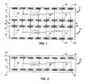
- FIG. 1is an illustration of an embodiment of mated three-dimensional coupling connectors in accordance with the invention.
- FIG. 2is an illustration of an embodiment of a three-dimensional coupling connector in accordance with the invention.
- FIG. 3is an illustration of a mated pair of electromagnetic coupling elements configured for unidirectional communication in accordance with an embodiment of the invention.
- FIG. 4is an illustration of a mated pair of electromagnetic coupling elements configured for bi-directional communication in accordance with an embodiment of the invention.
- FIG. 5is an illustration of serial pairs of mated coupling elements in accordance with an embodiment of the invention.
- FIG. 6is an illustration of mated capacitive coupling elements in accordance with an embodiment of the invention.
- FIG. 7is an illustration of mated inductive coupling elements in accordance with an embodiment of the invention.
- FIG. 8is an illustration of an embodiment of a three-dimensional circuit in accordance with the invention.
- FIG. 9is a side view illustration of the three-dimensional circuit of FIG. 8 .
- FIG. 10is an illustration of an embodiment of a three-dimensional circuit in accordance with the invention.
- the present inventionrelates to a reliable high-density, low-cost electromagnetic coupling connector that can be connected and disconnected many times.
- the coupling connectoris resistant to wear, corrosion, dust and repeated thermal stress.
- the coupling connectorcan operate with a mating coupling connector across a small gap.
- the coupling connectorcan operate while in contact with the mated coupling connector.
- Multiple coupling connectorscan be used to couple vertically stacked circuit layers, including layers having analog and digital processing modules.
- FIG. 1depicts a pair of three-dimensional coupling connectors 10 and 10 ′ according to the present invention.
- the connectors 10 , 10 ′are shown coupled to one another for transmitting and receiving data signals by electromagnetic communication.
- Primed referencesare used to identify components of coupling connector 10 ′ that are similar to their unprimed counterparts in coupling connector 10 .
- the coupling connector 10is fabricated as a single planar structure and includes an upper coupling layer 14 , a lower coupling layer 18 and a routing layer 22 .
- Each coupling layer 14 , 18includes a set of electromagnetic coupling elements 26 which can be separated in the plane of the layer 14 , 18 by air or by a non-conducting material. The location of at least one of the coupling elements 26 is selected to permit alignment with one or more respective coupling elements 26 ′ in the adjacent coupling connector 10 ′.
- the coupling elements 26 in the lower coupling layer 18 of coupling connector 10are arranged to mate with at least some of the coupling elements 26 ′ in the upper coupling layer 14 ′ of coupling connector 10 ′.
- a mated coupling elementis defined as a coupling element 26 that is positioned in close proximity to another coupling element 26 ′ in a different coupling connector 10 to establish a path (depicted as bi-directional arrows) between the elements 26 , 26 ′ for the transmission of electromagnetic signals.
- a coupling element 26 in one connector 10can be mated with more than one coupling element 26 ′ in a second connector 26 ′, for example by using coupling elements 26 , 26 ′ that differ in size, the description below is limited to one-to-one mated coupling elements 26 , 26 ′.
- Coupling elements 26can be distributed in the coupling layers 14 , 18 in any two-dimensional arrangement, including various arrays and linear configurations. Aligned coupling connectors 10 , 10 ′ enable communication of time-dependent electrical signals through electromagnetic paths established between the mated coupling element pairs 26 , 26 ′ across an air gap 30 .
- the routing layer 22provides conductive paths 34 between the coupling elements 26 in the top coupling layer 14 and the coupling elements 26 in the bottom coupling layer 18 .
- the conductive paths 34can take any direction and length within the routing layer 22 .
- the conductive paths 34are shown to pass horizontally and vertically (i.e., within the thickness of the routing layer 22 ) to indicate connected coupling elements 26 . It should be recognized, however, that the conductive paths 34 can be fabricated on the top and/or bottom surfaces of the routing layer 22 .
- the conductive pathscan be embedded in one or more planes within the thickness of the routing layer 22 , for example, by fabricating multiple conducting layers each etched to form electrical traces. In this example, each conducting layer is separated from an adjacent conducting layer by an insulating layer.
- two or more routing layers 22are included in the coupling connector 10 .
- the conductive paths 34are primarily two-dimensional because the routing is achieved within a plane of the routing layer 22 , the conductive paths 34 generally include pathways (e.g., via holes) that pass vertically through the routing layer 22 to permit complete paths between the coupling elements 26 in opposite coupling layers 14 , 18 .
- the routing layer 22can include any number of conductive planes. Some conductive paths 34 provide an electrical connection between a coupling element 26 in the upper coupling layer 14 and at least one coupling element 26 in the lower coupling layer 18 . Other conductive paths 34 provide an electrical connection between coupling elements 26 within the same coupling layer 14 , 18 . Still other conductive paths 34 provide an electrical connection between a coupling element 26 in the top coupling layer 14 with at least one other coupling element 26 in the top coupling layer 14 and at least one coupling element 26 in the lower coupling layer 18 .
- FIG. 2illustrates an embodiment of a three-dimensional coupling connector 38 having improved durability.
- the coupling connector 38is similar to the coupling connector 10 of FIG. 1 but also includes a dielectric layer 42 fabricated over each of the coupling layers 14 and 18 , respectively.
- the dielectric layers 42enable the coupling connector 38 to be connected to another coupling connector through direct physical contact of the connectors 38 without subjecting the coupling elements 26 to potentially damaging contact.
- there is no air gap 30 (see FIG. 1 ) between the connectors 38there is no means for dust to intrude between the coupling elements 26 .
- the dielectric layers 42seal, or encapsulate, the coupling elements 26 thereby preventing corrosion that can otherwise result from exposure to air and moisture.
- one of the dielectric layers 42can be omitted if the coupling connector 38 is intended to be coupled to another coupling connector at only one side (i.e., coupling layer 14 or coupling layer 18 ).
- FIG. 3shows a pair of mated coupling elements 26 and 26 ′ from the coupling connectors 10 and 10 ′, respectively, of FIG. 1 configured for unidirectional communication.
- Each coupling element 26 , 26 ′is protected by a portion of the adjacent dielectric layers 42 , 42 ′, respectively.
- Coupling element 26is in electrical communication with a transmit driver circuit 46 and coupling element 26 ′ is in electrical communication with a receiver circuit 50 .
- the transmit driver circuit 46 and receiver circuit 50can be fabricated near their respective coupling elements 26 , 26 ′ or can be fabricated farther away and coupled to the coupling elements 26 , 26 ′ by wires or transmission lines.
- the transmit driver circuit 46 and the receiver circuit 50are fabricated in a device layer (described below).
- connections to the coupling elements 26 , 26 ′can be single ended or double ended (i.e., two electrical paths) according to the type of coupling elements, signal integrity requirements, and whether a common reference voltage (i.e., ground) is available for both coupling elements 26 , 26 ′.
- a data signal provided by the transmit driver circuit 46 and transmit coupling element 26is electromagnetically communicated across an air gap 30 between the coupling elements 26 , 26 ′ and converted to an electrical data output signal by the receiving coupling element 26 ′ and receiver circuit 50 .
- the illustrationshows the coupling elements 26 , 26 ′ as separated by the dielectric layers 42 , 42 ′ and the air gap 30 , the dielectric layers 42 , 42 ′ can be in contact (i.e., no air gap) and electromagnetic communication between the coupling elements 26 , 26 ′ is possible.
- one or more of the coupling elements 26 , 26 ′, transmit drive circuit 46 and receiver circuit 50can include impedance matching networks for improving signal transfer or to prevent signal reflections.
- bi-directional communication between mated coupling elements 26 , 26 ′is possible by replacing the transmit driver circuit 46 and receiver circuit 50 with transceiver circuits 54 as shown in FIG. 4 .
- FIG. 5illustrates serial pairs of mated coupling elements 26 , 26 ′ (only two pairs shown for clarity).
- a data signalcan be transmitted through multiple coupling connectors. Because intermediate routing layers are constructed to conduct electrical signals laterally (i.e., through paths within the plane of each routing layer), it is possible to communicate a data signal from one coupling element 26 to any other coupling element 26 in any coupling connector in the same three-dimensional structure.
- FIG. 6illustrates a portion of two communicating coupling connectors 38 , 38 ′ (see FIG. 2 ).
- Each coupling connector 38 , 38 ′includes a coupling layer 18 and 14 ′, respectively, having double-ended capacitive coupling elements 58 and 58 ′, respectively, for differential signal transfer.
- One capacitive coupling element 58is coupled to a transmit driver circuit 46 the other capacitive coupling element 58 ′ is coupled to a receiver circuit 50 .
- the capacitive coupling elements 58 , 58 ′are fabricated as flat conductive pads.
- the padscan be circular, rectangular, hexagonal, or other shape. In other embodiments, the pads are non-planar structures such as portions of cylinders or spheres.
- any number of padscan be configured to operate as a single coupling element 58 , 58 ′.
- the capacitive coupling connectors 38 , 38 ′are aligned to reduce or eliminate any offset between the mated pads as measured in the planes of the pads to achieve increased capacitance.
- the gap 30 between the padsis minimized to further increase capacitance.
- the dielectric layers 42 , 42 ′are fabricated using materials having large dielectric constants. Electrolytic materials can be used for even greater capacitance.
- FIG. 7illustrates two mated inductive coupling elements 62 , 62 ′ configured for unidirectional communication.
- the inductive coupling elements 62 , 62 ′are coupled to a transmit driver circuit 46 and a receiver circuit 50 , respectively.
- Each inductive coupling element 62 , 62 ′is fabricated as an electrical coil or spiral.
- the coil cross-sectional shapecan be, for example, circular, rectangular or hexagonal.
- a single inductive coupling element 62 , 62 ′can be fabricated as multiple coils. Minimal lateral offset and minimum separation between the mated coupling elements 62 , 62 ′ is desired.
- ferrite materialis used to reduce the lateral extent of the electromagnetic field generated between the mated inductive coupling elements 62 , 62 ′. Consequently, the minimum distance between adjacent inductive coupling elements 62 , 62 ′ in the same coupling layer 14 , 18 (see FIG. 2 ) for non-interfering operation is reduced and a higher density of inductive coupling elements 62 , 62 ′ is possible.
- Both capacitive and inductive coupling elementscan be used in the same coupling connector if there is no substantial electromagnetic interference at one of the coupling elements resulting from the overlap of the generated electromagnetic field from the other coupling element.
- each type of coupling elementis used to transmit or receive a specific signal type.
- capacitive couplingcan be used for high-speed data signals and inductive coupling can be used to supply power in a non-interfering manner.
- both types of coupling elementsare combined as a single coupling element to increase the signal quality (e.g., signal-to-noise ratio).
- FIG. 8depicts a three-dimensional circuit 66 in accordance with the present invention and FIG. 9 depicts a side view of the circuit 66 of FIG. 8 .
- the illustrated embodimentshows three circuit layers 70 in the three-dimensional circuit 66 , although any number of circuit layers 70 is contemplated by the present invention.
- a circuit layer 70can be any circuit that is implemented in a substantially planar structure.
- a circuit layer 70can include a circuit board having very large-scale integration (VLSI) processors and/or multi-chip modules (MCMs).
- VLSIvery large-scale integration
- MCMsmulti-chip modules
- Each circuit layer 70includes an upper coupling layer 14 , a two-dimensional routing layer 22 , a device layer 74 , a thermally-conductive layer 78 and a lower coupling layer 18 .
- the upper and lower coupling layers 14 , 18are covered by dielectric layers 42 .
- the thermal expansion coefficients of the various layersare similar to reduce thermal stress. In one embodiment, the thermal expansion coefficients of the layers are approximately equal to the thermal expansion coefficient of silicon.
- Each device layer 74includes one or more electronic modules or devices 82 .
- the devices 82are used for processing data, providing active switching functionality or performing specialized functions.
- the devices 74can be analog processors, digital processors, switching modules and memory modules.
- multiple device layers 74are fabricated in a single circuit layer 70 .
- Thermally-conductive layer 78provides a thermal path to conduct heat from the devices 82 to a heat sink structure such as the cold plates 86 shown in the three-dimensional circuit 66 ′ of FIG. 10 .
- Multiple thermally-conductive layers 78can be included in a single circuit layer 70 to improve thermal management. Heat can be removed from the cold plates in many ways, for example, by air convection or liquid cooling.
- Thermally-conductive layers 78include via holes for conductive paths by which electrical signals can pass.
- the thermally-conductive layers 78are fabricated from a material having high thermal conductivity, such as a silicon or graphite substrate.
- passive micro heat pipesare embedded in the thermally-conductive layer 78 .
- an active liquid cooling systemis embedded in the thermally-conductive layer 78 .
- the inventionis not limited to a coupling connector having a single routing layer, a single device layer and a single thermally-conductive layer.
- the coupling connector of the inventioncan include multiple layers of various types according to the requirements of the specific connector application.
Landscapes
- Engineering & Computer Science (AREA)
- Power Engineering (AREA)
- Microelectronics & Electronic Packaging (AREA)
- Physics & Mathematics (AREA)
- Condensed Matter Physics & Semiconductors (AREA)
- General Physics & Mathematics (AREA)
- Computer Hardware Design (AREA)
- Details Of Connecting Devices For Male And Female Coupling (AREA)
Abstract
Description
Claims (21)
Priority Applications (3)
| Application Number | Priority Date | Filing Date | Title |
|---|---|---|---|
| US10/459,667US6891447B2 (en) | 2002-07-12 | 2003-06-11 | Electromagnetic coupling connector for three-dimensional electronic circuits |
| AU2003248734AAU2003248734A1 (en) | 2002-07-12 | 2003-06-24 | Electromagnetic coupling connector for three-dimensional electronic circuits |
| PCT/US2003/020258WO2004008577A2 (en) | 2002-07-12 | 2003-06-24 | Electromagnetic coupling connector for three-dimensional electronic circuits |
Applications Claiming Priority (2)
| Application Number | Priority Date | Filing Date | Title |
|---|---|---|---|
| US39545602P | 2002-07-12 | 2002-07-12 | |
| US10/459,667US6891447B2 (en) | 2002-07-12 | 2003-06-11 | Electromagnetic coupling connector for three-dimensional electronic circuits |
Publications (2)
| Publication Number | Publication Date |
|---|---|
| US20040095201A1 US20040095201A1 (en) | 2004-05-20 |
| US6891447B2true US6891447B2 (en) | 2005-05-10 |
Family
ID=30118509
Family Applications (1)
| Application Number | Title | Priority Date | Filing Date |
|---|---|---|---|
| US10/459,667Expired - Fee RelatedUS6891447B2 (en) | 2002-07-12 | 2003-06-11 | Electromagnetic coupling connector for three-dimensional electronic circuits |
Country Status (3)
| Country | Link |
|---|---|
| US (1) | US6891447B2 (en) |
| AU (1) | AU2003248734A1 (en) |
| WO (1) | WO2004008577A2 (en) |
Cited By (20)
| Publication number | Priority date | Publication date | Assignee | Title |
|---|---|---|---|---|
| US20040253874A1 (en)* | 2003-01-15 | 2004-12-16 | Plishner Paul J. | Connector or other circuit element having an indirectly coupled integrated circuit |
| US20060284715A1 (en)* | 2005-06-21 | 2006-12-21 | Camarena Villasenor Jose D J | Energy saving system for a unit requiring electricity |
| US20060283006A1 (en)* | 2005-06-21 | 2006-12-21 | Camarena Villasenor Jose D J | Method of manufacture of magnetic induction devices |
| US20080136424A1 (en)* | 2006-12-06 | 2008-06-12 | Alex Chow | Determining chip separation by comparing coupling capacitances |
| US20090130885A1 (en)* | 2007-11-15 | 2009-05-21 | Juergen Hagen | Plug connection device designed to connect two function elements for signal and power transmission |
| US20110201154A1 (en)* | 2005-05-09 | 2011-08-18 | Elpida Memory, Inc. | Semiconductor device including stacked semiconductor chips |
| US8150266B1 (en)* | 2003-09-12 | 2012-04-03 | Oracle America, Inc. | Method and apparatus for performing butterfly differential signaling |
| US20120125676A1 (en)* | 2006-01-13 | 2012-05-24 | Panasonic Corporation | Three-dimensional circuit board and its manufacturing method |
| US20130314181A1 (en)* | 2012-05-28 | 2013-11-28 | Sony Corporation | Coupler |
| US20130342287A1 (en)* | 2012-06-25 | 2013-12-26 | Dielectric Laboratories, Inc. | High frequency band pass filter with coupled surface mount transition |
| US8751556B2 (en) | 2010-06-11 | 2014-06-10 | Massachusetts Institute Of Technology | Processor for large graph algorithm computations and matrix operations |
| US8933540B2 (en) | 2013-02-28 | 2015-01-13 | International Business Machines Corporation | Thermal via for 3D integrated circuits structures |
| US10719762B2 (en)* | 2017-08-03 | 2020-07-21 | Xcelsis Corporation | Three dimensional chip structure implementing machine trained network |
| US10886177B2 (en) | 2016-10-07 | 2021-01-05 | Xcelsis Corporation | 3D chip with shared clock distribution network |
| US10892252B2 (en) | 2016-10-07 | 2021-01-12 | Xcelsis Corporation | Face-to-face mounted IC dies with orthogonal top interconnect layers |
| US10950547B2 (en) | 2016-10-07 | 2021-03-16 | Xcelsis Corporation | Stacked IC structure with system level wiring on multiple sides of the IC die |
| US10978348B2 (en) | 2016-10-07 | 2021-04-13 | Xcelsis Corporation | 3D chip sharing power interconnect layer |
| US11152336B2 (en) | 2016-10-07 | 2021-10-19 | Xcelsis Corporation | 3D processor having stacked integrated circuit die |
| US11289333B2 (en) | 2016-10-07 | 2022-03-29 | Xcelsis Corporation | Direct-bonded native interconnects and active base die |
| US11599299B2 (en) | 2019-11-19 | 2023-03-07 | Invensas Llc | 3D memory circuit |
Families Citing this family (7)
| Publication number | Priority date | Publication date | Assignee | Title |
|---|---|---|---|---|
| DE102012204556A1 (en)* | 2012-03-21 | 2013-09-26 | Schleifring Und Apparatebau Gmbh | Contactless plug |
| US9106270B2 (en)* | 2012-10-02 | 2015-08-11 | Covidien Lp | Transmitting data across a patient isolation barrier using an electric-field capacitive coupler module |
| EP3250892B1 (en) | 2015-01-28 | 2019-10-16 | Continental Teves AG & Co. OHG | Adapter with embedded filter components for sensors |
| WO2016120272A1 (en) | 2015-01-28 | 2016-08-04 | Continental Teves Ag & Co. Ohg | Sensor with symmetrically embedded sensor elements |
| US9645619B2 (en)* | 2015-05-29 | 2017-05-09 | Corsair Memory, Inc. | Micro heat pipe cooling system |
| DE102015115975A1 (en)* | 2015-09-22 | 2017-03-23 | Endress+Hauser Conducta Gmbh+Co. Kg | Connecting element for a sensor or a connection element of process automation |
| US20190252321A1 (en)* | 2016-09-28 | 2019-08-15 | Intel Corporation | Interconnector with bundled interconnects |
Citations (15)
| Publication number | Priority date | Publication date | Assignee | Title |
|---|---|---|---|---|
| US3742408A (en) | 1969-12-12 | 1973-06-26 | Bissett Berman Corp | Inductively coupled connector |
| US4038625A (en) | 1976-06-07 | 1977-07-26 | General Electric Company | Magnetic inductively-coupled connector |
| GB2149548A (en) | 1983-10-27 | 1985-06-12 | Robert Philp | Contact-less electronic connectors |
| US4884982A (en) | 1989-04-03 | 1989-12-05 | Amp Incorporated | Capacitive coupled connector |
| US5119172A (en) | 1991-03-04 | 1992-06-02 | Motorola, Inc. | Microelectronic device package employing capacitively coupled connections |
| US5212115A (en) | 1991-03-04 | 1993-05-18 | Motorola, Inc. | Method for microelectronic device packaging employing capacitively coupled connections |
| US5432486A (en) | 1993-05-20 | 1995-07-11 | Northern Telecom Limited | Capacitive and inductive coupling connector |
| US5557068A (en) | 1995-11-28 | 1996-09-17 | D-Link Corporation | Capacitive coupled BNC connector |
| US5786979A (en) | 1995-12-18 | 1998-07-28 | Douglass; Barry G. | High density inter-chip connections by electromagnetic coupling |
| US5818748A (en) | 1995-11-21 | 1998-10-06 | International Business Machines Corporation | Chip function separation onto separate stacked chips |
| US5821625A (en) | 1995-04-24 | 1998-10-13 | Matsushita Electric Industrial Co., Ltd. | Structure of chip on chip mounting preventing from crosstalk noise |
| US5995379A (en)* | 1997-10-30 | 1999-11-30 | Nec Corporation | Stacked module and substrate therefore |
| US6033263A (en) | 1996-10-15 | 2000-03-07 | The Whitaker Corporation | Electrically connector with capacitive coupling |
| US6559531B1 (en) | 1999-10-14 | 2003-05-06 | Sun Microsystems, Inc. | Face to face chips |
| US6717251B2 (en) | 2000-09-28 | 2004-04-06 | Kabushiki Kaisha Toshiba | Stacked type semiconductor device |
- 2003
- 2003-06-11USUS10/459,667patent/US6891447B2/ennot_activeExpired - Fee Related
- 2003-06-24WOPCT/US2003/020258patent/WO2004008577A2/ennot_activeApplication Discontinuation
- 2003-06-24AUAU2003248734Apatent/AU2003248734A1/ennot_activeAbandoned
Patent Citations (15)
| Publication number | Priority date | Publication date | Assignee | Title |
|---|---|---|---|---|
| US3742408A (en) | 1969-12-12 | 1973-06-26 | Bissett Berman Corp | Inductively coupled connector |
| US4038625A (en) | 1976-06-07 | 1977-07-26 | General Electric Company | Magnetic inductively-coupled connector |
| GB2149548A (en) | 1983-10-27 | 1985-06-12 | Robert Philp | Contact-less electronic connectors |
| US4884982A (en) | 1989-04-03 | 1989-12-05 | Amp Incorporated | Capacitive coupled connector |
| US5119172A (en) | 1991-03-04 | 1992-06-02 | Motorola, Inc. | Microelectronic device package employing capacitively coupled connections |
| US5212115A (en) | 1991-03-04 | 1993-05-18 | Motorola, Inc. | Method for microelectronic device packaging employing capacitively coupled connections |
| US5432486A (en) | 1993-05-20 | 1995-07-11 | Northern Telecom Limited | Capacitive and inductive coupling connector |
| US5821625A (en) | 1995-04-24 | 1998-10-13 | Matsushita Electric Industrial Co., Ltd. | Structure of chip on chip mounting preventing from crosstalk noise |
| US5818748A (en) | 1995-11-21 | 1998-10-06 | International Business Machines Corporation | Chip function separation onto separate stacked chips |
| US5557068A (en) | 1995-11-28 | 1996-09-17 | D-Link Corporation | Capacitive coupled BNC connector |
| US5786979A (en) | 1995-12-18 | 1998-07-28 | Douglass; Barry G. | High density inter-chip connections by electromagnetic coupling |
| US6033263A (en) | 1996-10-15 | 2000-03-07 | The Whitaker Corporation | Electrically connector with capacitive coupling |
| US5995379A (en)* | 1997-10-30 | 1999-11-30 | Nec Corporation | Stacked module and substrate therefore |
| US6559531B1 (en) | 1999-10-14 | 2003-05-06 | Sun Microsystems, Inc. | Face to face chips |
| US6717251B2 (en) | 2000-09-28 | 2004-04-06 | Kabushiki Kaisha Toshiba | Stacked type semiconductor device |
Non-Patent Citations (3)
| Title |
|---|
| Berard et al., Capacitive Coupled Connector, IBM Technical Disclosure Bulletin, Jul. 1975, p. 355-6. |
| Krembs, Capacitive-coupled Connectors for Gaseuous . . . , IBM Technical Disclosure Bulletin, Apr. 1971. |
| Kuijk et al., Integration of CMOS-VLSI and . . . , Electronics Letters, Oct. 9, 1997, p. 1778-9, vol. 33 No. 21. |
Cited By (54)
| Publication number | Priority date | Publication date | Assignee | Title |
|---|---|---|---|---|
| US20040253874A1 (en)* | 2003-01-15 | 2004-12-16 | Plishner Paul J. | Connector or other circuit element having an indirectly coupled integrated circuit |
| US7869974B2 (en)* | 2003-01-15 | 2011-01-11 | Plishner Paul J | Connector or other circuit element having an indirectly coupled integrated circuit |
| US8150266B1 (en)* | 2003-09-12 | 2012-04-03 | Oracle America, Inc. | Method and apparatus for performing butterfly differential signaling |
| US7395166B2 (en) | 2004-05-06 | 2008-07-01 | Paul J. Plishner | Connector including an integrated circuit powered by a connection to a conductor terminating in the connector |
| US9640243B2 (en) | 2005-05-09 | 2017-05-02 | Longitude Semiconductor S.A.R.L. | Semiconductor device including stacked semiconductor chips |
| US20110201154A1 (en)* | 2005-05-09 | 2011-08-18 | Elpida Memory, Inc. | Semiconductor device including stacked semiconductor chips |
| US8907463B2 (en)* | 2005-05-09 | 2014-12-09 | Ps4 Luxco S.A.R.L. | Semiconductor device including stacked semiconductor chips |
| US9048239B2 (en) | 2005-05-09 | 2015-06-02 | Ps4 Luxco S.A.R.L. | Semiconductor device including stacked semiconductor chips |
| US7183890B2 (en) | 2005-06-21 | 2007-02-27 | Jose De Jesus Camarena Villaseñor | Magnetic induction device |
| US7511445B2 (en) | 2005-06-21 | 2009-03-31 | Camarena Villasenor Jose De Jesus | Method of manufacture of magnetic induction devices |
| US7295097B2 (en) | 2005-06-21 | 2007-11-13 | Camarena Villasenor Jose De Je | Energy saving system for a unit requiring electricity |
| US20060283006A1 (en)* | 2005-06-21 | 2006-12-21 | Camarena Villasenor Jose D J | Method of manufacture of magnetic induction devices |
| US20060284714A1 (en)* | 2005-06-21 | 2006-12-21 | Camarena Villasenor Jose D J | Magnetic induction device |
| US20060284715A1 (en)* | 2005-06-21 | 2006-12-21 | Camarena Villasenor Jose D J | Energy saving system for a unit requiring electricity |
| US8809693B2 (en)* | 2006-01-13 | 2014-08-19 | Panasonic Corporation | Three-dimensional circuit board |
| US20120125676A1 (en)* | 2006-01-13 | 2012-05-24 | Panasonic Corporation | Three-dimensional circuit board and its manufacturing method |
| US20080136424A1 (en)* | 2006-12-06 | 2008-06-12 | Alex Chow | Determining chip separation by comparing coupling capacitances |
| US7871833B2 (en) | 2006-12-06 | 2011-01-18 | Oracle America, Inc. | Determining chip separation by comparing coupling capacitances |
| US20100060299A1 (en)* | 2006-12-06 | 2010-03-11 | Sun Microsystems, Inc. | Determining chip separation by comparing coupling capacitances |
| US7649255B2 (en)* | 2006-12-06 | 2010-01-19 | Sun Microsystems, Inc. | Determining chip separation by comparing coupling capacitances |
| US7722375B2 (en) | 2007-11-15 | 2010-05-25 | Siemens Aktiengesellschaft | Plug connection device designed to connect two function elements for signal and power transmission |
| DE102007054592B4 (en)* | 2007-11-15 | 2014-04-30 | Siemens Aktiengesellschaft | Plug connection device, designed to connect two functional elements for signal and power transmission |
| DE102007054592A1 (en)* | 2007-11-15 | 2009-05-28 | Siemens Ag | Plug connection device, designed to connect two functional elements for signal and power transmission |
| US20090130885A1 (en)* | 2007-11-15 | 2009-05-21 | Juergen Hagen | Plug connection device designed to connect two function elements for signal and power transmission |
| US9529590B2 (en) | 2010-06-11 | 2016-12-27 | Massachusetts Institute Of Technology | Processor for large graph algorithm computations and matrix operations |
| US8751556B2 (en) | 2010-06-11 | 2014-06-10 | Massachusetts Institute Of Technology | Processor for large graph algorithm computations and matrix operations |
| US9246548B2 (en)* | 2012-05-28 | 2016-01-26 | Sony Corporation | Electromagnetic coupling of electronic devices using resonant terminations that shift resonant frequencies |
| US20130314181A1 (en)* | 2012-05-28 | 2013-11-28 | Sony Corporation | Coupler |
| US9490768B2 (en)* | 2012-06-25 | 2016-11-08 | Knowles Cazenovia Inc. | High frequency band pass filter with coupled surface mount transition |
| US20130342287A1 (en)* | 2012-06-25 | 2013-12-26 | Dielectric Laboratories, Inc. | High frequency band pass filter with coupled surface mount transition |
| US9812750B2 (en) | 2012-06-25 | 2017-11-07 | Knowles Cazenovia Inc. | High frequency band pass filter with coupled surface mount transition |
| US8933540B2 (en) | 2013-02-28 | 2015-01-13 | International Business Machines Corporation | Thermal via for 3D integrated circuits structures |
| US11823906B2 (en) | 2016-10-07 | 2023-11-21 | Xcelsis Corporation | Direct-bonded native interconnects and active base die |
| US12218059B2 (en) | 2016-10-07 | 2025-02-04 | Adeia Semiconductor Inc. | Stacked IC structure with orthogonal interconnect layers |
| US10892252B2 (en) | 2016-10-07 | 2021-01-12 | Xcelsis Corporation | Face-to-face mounted IC dies with orthogonal top interconnect layers |
| US10950547B2 (en) | 2016-10-07 | 2021-03-16 | Xcelsis Corporation | Stacked IC structure with system level wiring on multiple sides of the IC die |
| US12401010B2 (en) | 2016-10-07 | 2025-08-26 | Adeia Semiconductor Inc. | 3D processor having stacked integrated circuit die |
| US10978348B2 (en) | 2016-10-07 | 2021-04-13 | Xcelsis Corporation | 3D chip sharing power interconnect layer |
| US11152336B2 (en) | 2016-10-07 | 2021-10-19 | Xcelsis Corporation | 3D processor having stacked integrated circuit die |
| US12362182B2 (en) | 2016-10-07 | 2025-07-15 | Adeia Semiconductor Inc. | Direct-bonded native interconnects and active base die |
| US11289333B2 (en) | 2016-10-07 | 2022-03-29 | Xcelsis Corporation | Direct-bonded native interconnects and active base die |
| US11557516B2 (en) | 2016-10-07 | 2023-01-17 | Adeia Semiconductor Inc. | 3D chip with shared clock distribution network |
| US12293993B2 (en) | 2016-10-07 | 2025-05-06 | Adeia Semiconductor Inc. | 3D chip sharing data bus |
| US10886177B2 (en) | 2016-10-07 | 2021-01-05 | Xcelsis Corporation | 3D chip with shared clock distribution network |
| US11824042B2 (en) | 2016-10-07 | 2023-11-21 | Xcelsis Corporation | 3D chip sharing data bus |
| US12142528B2 (en) | 2016-10-07 | 2024-11-12 | Adeia Semiconductor Inc. | 3D chip with shared clock distribution network |
| US11881454B2 (en) | 2016-10-07 | 2024-01-23 | Adeia Semiconductor Inc. | Stacked IC structure with orthogonal interconnect layers |
| US10719762B2 (en)* | 2017-08-03 | 2020-07-21 | Xcelsis Corporation | Three dimensional chip structure implementing machine trained network |
| US11790219B2 (en) | 2017-08-03 | 2023-10-17 | Adeia Semiconductor Inc. | Three dimensional circuit implementing machine trained network |
| US12248869B2 (en) | 2017-08-03 | 2025-03-11 | Adeia Semiconductor Inc. | Three dimensional circuit implementing machine trained network |
| US11176450B2 (en) | 2017-08-03 | 2021-11-16 | Xcelsis Corporation | Three dimensional circuit implementing machine trained network |
| US10970627B2 (en) | 2017-08-03 | 2021-04-06 | Xcelsis Corporation | Time borrowing between layers of a three dimensional chip stack |
| US11599299B2 (en) | 2019-11-19 | 2023-03-07 | Invensas Llc | 3D memory circuit |
| US12293108B2 (en) | 2019-11-19 | 2025-05-06 | Adeia Semiconductor Technologies Llc | 3D memory circuit |
Also Published As
| Publication number | Publication date |
|---|---|
| AU2003248734A8 (en) | 2004-02-02 |
| US20040095201A1 (en) | 2004-05-20 |
| AU2003248734A1 (en) | 2004-02-02 |
| WO2004008577A2 (en) | 2004-01-22 |
| WO2004008577A3 (en) | 2004-08-19 |
Similar Documents
| Publication | Publication Date | Title |
|---|---|---|
| US6891447B2 (en) | Electromagnetic coupling connector for three-dimensional electronic circuits | |
| US6932618B1 (en) | Mezzanine integrated circuit interconnect | |
| US7473102B2 (en) | Space transforming land grid array interposers | |
| US6884086B1 (en) | System and method for connecting a power converter to a land grid array socket | |
| CN111954955A (en) | Integrated antenna array package structure and method | |
| US8446738B2 (en) | Motherboard assembly for interconnecting and distributing signals and power | |
| US7425760B1 (en) | Multi-chip module structure with power delivery using flexible cables | |
| US11715912B2 (en) | Interposer having shielded contacts and traces | |
| US12255424B2 (en) | Electrical interposer with shielded contacts and shielding ground plane with optimized impedance response | |
| US6396710B1 (en) | High density interconnect module | |
| US7068120B2 (en) | Electromagnetic bus coupling having an electromagnetic coupling interposer | |
| US9426918B2 (en) | Socket package including integrataed capacitors | |
| WO2022212604A1 (en) | Interconnect alignment system and method | |
| WO2020135561A1 (en) | Chip and backplane connector interconnection apparatus, and communications device | |
| CN118946245B (en) | Quantum chip packaging device, integrated circuit and assembly method | |
| US20240356255A1 (en) | Array of compliant connectors for electronic assemblies | |
| JP3701242B2 (en) | Connection system | |
| Chen et al. | An overview of electrical and mechanical aspects of electronic packaging | |
| CN115966928A (en) | electrical connection device | |
| TW202308080A (en) | Electrical connection device characterized in that it is beneficial for a detachable electrical connection in response to a tiny scale and the shield of signal transmission can be generated | |
| KR20230122783A (en) | Electrical connector for signal transmission |
Legal Events
| Date | Code | Title | Description |
|---|---|---|---|
| AS | Assignment | Owner name:MASSACHUSETTS INSTITUTE OF TECHNOLO, MASSACHUSETTS Free format text:ASSIGNMENT OF ASSIGNORS INTEREST;ASSIGNOR:SONG, WILLIAM S.;REEL/FRAME:014179/0236 Effective date:20030610 | |
| AS | Assignment | Owner name:AIR FORCE, UNITED STATES, MASSACHUSETTS Free format text:CONFIRMATORY LICENSE;ASSIGNOR:MASSACHUSETTS INSTITUTE OF TECHNOLOGY, LINCOLN LABORATORY;REEL/FRAME:014345/0577 Effective date:20030711 | |
| FEPP | Fee payment procedure | Free format text:PAYOR NUMBER ASSIGNED (ORIGINAL EVENT CODE: ASPN); ENTITY STATUS OF PATENT OWNER: MICROENTITY | |
| FPAY | Fee payment | Year of fee payment:4 | |
| FEPP | Fee payment procedure | Free format text:PAYER NUMBER DE-ASSIGNED (ORIGINAL EVENT CODE: RMPN); ENTITY STATUS OF PATENT OWNER: MICROENTITY Free format text:PAYOR NUMBER ASSIGNED (ORIGINAL EVENT CODE: ASPN); ENTITY STATUS OF PATENT OWNER: MICROENTITY | |
| FPAY | Fee payment | Year of fee payment:8 | |
| FEPP | Fee payment procedure | Free format text:PATENT HOLDER CLAIMS MICRO ENTITY STATUS, ENTITY STATUS SET TO MICRO (ORIGINAL EVENT CODE: STOM); ENTITY STATUS OF PATENT OWNER: MICROENTITY | |
| REMI | Maintenance fee reminder mailed | ||
| LAPS | Lapse for failure to pay maintenance fees | ||
| STCH | Information on status: patent discontinuation | Free format text:PATENT EXPIRED DUE TO NONPAYMENT OF MAINTENANCE FEES UNDER 37 CFR 1.362 | |
| FP | Lapsed due to failure to pay maintenance fee | Effective date:20170510 |