US6890596B2 - Deposition methods - Google Patents
Deposition methodsDownload PDFInfo
- Publication number
- US6890596B2 US6890596B2US10/222,304US22230402AUS6890596B2US 6890596 B2US6890596 B2US 6890596B2US 22230402 AUS22230402 AUS 22230402AUS 6890596 B2US6890596 B2US 6890596B2
- Authority
- US
- United States
- Prior art keywords
- chamber
- purge gas
- substrate
- reactive
- deposition
- Prior art date
- Legal status (The legal status is an assumption and is not a legal conclusion. Google has not performed a legal analysis and makes no representation as to the accuracy of the status listed.)
- Expired - Fee Related, expires
Links
- 238000000151depositionMethods0.000titleclaimsabstractdescription143
- 238000010926purgeMethods0.000claimsabstractdescription211
- 239000000758substrateSubstances0.000claimsabstractdescription175
- 230000008021depositionEffects0.000claimsabstractdescription114
- 238000000034methodMethods0.000claimsabstractdescription103
- 239000000463materialSubstances0.000claimsabstractdescription78
- 238000005229chemical vapour depositionMethods0.000claimsdescription21
- 239000006227byproductSubstances0.000claimsdescription16
- 238000000231atomic layer depositionMethods0.000claimsdescription13
- 239000000203mixtureSubstances0.000claimsdescription11
- 239000002131composite materialSubstances0.000claimsdescription2
- 239000007789gasSubstances0.000description106
- 239000002243precursorSubstances0.000description19
- 239000010410layerSubstances0.000description14
- CBENFWSGALASAD-UHFFFAOYSA-NOzoneChemical compound[O-][O+]=OCBENFWSGALASAD-UHFFFAOYSA-N0.000description8
- 239000002356single layerSubstances0.000description8
- 125000004430oxygen atomChemical groupO*0.000description4
- 238000005240physical vapour depositionMethods0.000description4
- 239000011148porous materialSubstances0.000description4
- 239000004065semiconductorSubstances0.000description4
- 239000007806chemical reaction intermediateSubstances0.000description3
- 238000007599dischargingMethods0.000description3
- 239000000543intermediateSubstances0.000description3
- 239000000126substanceSubstances0.000description3
- 229910010068TiCl2Inorganic materials0.000description2
- 229910010062TiCl3Inorganic materials0.000description2
- 229910003074TiCl4Inorganic materials0.000description2
- ATJFFYVFTNAWJD-UHFFFAOYSA-NTinChemical group[Sn]ATJFFYVFTNAWJD-UHFFFAOYSA-N0.000description2
- PNEYBMLMFCGWSK-UHFFFAOYSA-Naluminium oxideInorganic materials[O-2].[O-2].[O-2].[Al+3].[Al+3]PNEYBMLMFCGWSK-UHFFFAOYSA-N0.000description2
- 238000000429assemblyMethods0.000description2
- 230000000712assemblyEffects0.000description2
- 230000015572biosynthetic processEffects0.000description2
- 238000004891communicationMethods0.000description2
- 239000000470constituentSubstances0.000description2
- 229910052593corundumInorganic materials0.000description2
- 230000000694effectsEffects0.000description2
- 239000000047productSubstances0.000description2
- 239000007787solidSubstances0.000description2
- XJDNKRIXUMDJCW-UHFFFAOYSA-Jtitanium tetrachlorideChemical compoundCl[Ti](Cl)(Cl)ClXJDNKRIXUMDJCW-UHFFFAOYSA-J0.000description2
- ZWYDDDAMNQQZHD-UHFFFAOYSA-Ltitanium(ii) chlorideChemical compound[Cl-].[Cl-].[Ti+2]ZWYDDDAMNQQZHD-UHFFFAOYSA-L0.000description2
- YONPGGFAJWQGJC-UHFFFAOYSA-Ktitanium(iii) chlorideChemical compoundCl[Ti](Cl)ClYONPGGFAJWQGJC-UHFFFAOYSA-K0.000description2
- JLTRXTDYQLMHGR-UHFFFAOYSA-NtrimethylaluminiumChemical compoundC[Al](C)CJLTRXTDYQLMHGR-UHFFFAOYSA-N0.000description2
- 229910001845yogo sapphireInorganic materials0.000description2
- QGZKDVFQNNGYKY-UHFFFAOYSA-NAmmoniaChemical classNQGZKDVFQNNGYKY-UHFFFAOYSA-N0.000description1
- 239000004809TeflonSubstances0.000description1
- 229920006362Teflon®Polymers0.000description1
- NRTOMJZYCJJWKI-UHFFFAOYSA-NTitanium nitrideChemical group[Ti]#NNRTOMJZYCJJWKI-UHFFFAOYSA-N0.000description1
- QVGXLLKOCUKJST-UHFFFAOYSA-Natomic oxygenChemical compound[O]QVGXLLKOCUKJST-UHFFFAOYSA-N0.000description1
- 238000004140cleaningMethods0.000description1
- 238000010276constructionMethods0.000description1
- 238000005137deposition processMethods0.000description1
- 239000000835fiberSubstances0.000description1
- 239000012530fluidSubstances0.000description1
- 229910000078germaneInorganic materials0.000description1
- 125000004435hydrogen atomChemical class[H]*0.000description1
- 229910010272inorganic materialInorganic materials0.000description1
- 239000011147inorganic materialSubstances0.000description1
- 239000007788liquidSubstances0.000description1
- 239000007791liquid phaseSubstances0.000description1
- 238000004519manufacturing processMethods0.000description1
- 239000002184metalSubstances0.000description1
- 229910052751metalInorganic materials0.000description1
- 239000002923metal particleSubstances0.000description1
- 238000012986modificationMethods0.000description1
- 230000004048modificationEffects0.000description1
- 239000011368organic materialSubstances0.000description1
- 239000001301oxygenSubstances0.000description1
- 229910052760oxygenInorganic materials0.000description1
- 230000000717retained effectEffects0.000description1
- 239000007790solid phaseSubstances0.000description1
- 238000001179sorption measurementMethods0.000description1
- 238000012876topographyMethods0.000description1
Images

Classifications
- C—CHEMISTRY; METALLURGY
- C23—COATING METALLIC MATERIAL; COATING MATERIAL WITH METALLIC MATERIAL; CHEMICAL SURFACE TREATMENT; DIFFUSION TREATMENT OF METALLIC MATERIAL; COATING BY VACUUM EVAPORATION, BY SPUTTERING, BY ION IMPLANTATION OR BY CHEMICAL VAPOUR DEPOSITION, IN GENERAL; INHIBITING CORROSION OF METALLIC MATERIAL OR INCRUSTATION IN GENERAL
- C23C—COATING METALLIC MATERIAL; COATING MATERIAL WITH METALLIC MATERIAL; SURFACE TREATMENT OF METALLIC MATERIAL BY DIFFUSION INTO THE SURFACE, BY CHEMICAL CONVERSION OR SUBSTITUTION; COATING BY VACUUM EVAPORATION, BY SPUTTERING, BY ION IMPLANTATION OR BY CHEMICAL VAPOUR DEPOSITION, IN GENERAL
- C23C16/00—Chemical coating by decomposition of gaseous compounds, without leaving reaction products of surface material in the coating, i.e. chemical vapour deposition [CVD] processes
- C23C16/44—Chemical coating by decomposition of gaseous compounds, without leaving reaction products of surface material in the coating, i.e. chemical vapour deposition [CVD] processes characterised by the method of coating
- C23C16/455—Chemical coating by decomposition of gaseous compounds, without leaving reaction products of surface material in the coating, i.e. chemical vapour deposition [CVD] processes characterised by the method of coating characterised by the method used for introducing gases into reaction chamber or for modifying gas flows in reaction chamber
- C23C16/45519—Inert gas curtains
- C—CHEMISTRY; METALLURGY
- C23—COATING METALLIC MATERIAL; COATING MATERIAL WITH METALLIC MATERIAL; CHEMICAL SURFACE TREATMENT; DIFFUSION TREATMENT OF METALLIC MATERIAL; COATING BY VACUUM EVAPORATION, BY SPUTTERING, BY ION IMPLANTATION OR BY CHEMICAL VAPOUR DEPOSITION, IN GENERAL; INHIBITING CORROSION OF METALLIC MATERIAL OR INCRUSTATION IN GENERAL
- C23C—COATING METALLIC MATERIAL; COATING MATERIAL WITH METALLIC MATERIAL; SURFACE TREATMENT OF METALLIC MATERIAL BY DIFFUSION INTO THE SURFACE, BY CHEMICAL CONVERSION OR SUBSTITUTION; COATING BY VACUUM EVAPORATION, BY SPUTTERING, BY ION IMPLANTATION OR BY CHEMICAL VAPOUR DEPOSITION, IN GENERAL
- C23C16/00—Chemical coating by decomposition of gaseous compounds, without leaving reaction products of surface material in the coating, i.e. chemical vapour deposition [CVD] processes
- C23C16/44—Chemical coating by decomposition of gaseous compounds, without leaving reaction products of surface material in the coating, i.e. chemical vapour deposition [CVD] processes characterised by the method of coating
- C23C16/4401—Means for minimising impurities, e.g. dust, moisture or residual gas, in the reaction chamber
- C—CHEMISTRY; METALLURGY
- C23—COATING METALLIC MATERIAL; COATING MATERIAL WITH METALLIC MATERIAL; CHEMICAL SURFACE TREATMENT; DIFFUSION TREATMENT OF METALLIC MATERIAL; COATING BY VACUUM EVAPORATION, BY SPUTTERING, BY ION IMPLANTATION OR BY CHEMICAL VAPOUR DEPOSITION, IN GENERAL; INHIBITING CORROSION OF METALLIC MATERIAL OR INCRUSTATION IN GENERAL
- C23C—COATING METALLIC MATERIAL; COATING MATERIAL WITH METALLIC MATERIAL; SURFACE TREATMENT OF METALLIC MATERIAL BY DIFFUSION INTO THE SURFACE, BY CHEMICAL CONVERSION OR SUBSTITUTION; COATING BY VACUUM EVAPORATION, BY SPUTTERING, BY ION IMPLANTATION OR BY CHEMICAL VAPOUR DEPOSITION, IN GENERAL
- C23C16/00—Chemical coating by decomposition of gaseous compounds, without leaving reaction products of surface material in the coating, i.e. chemical vapour deposition [CVD] processes
- C23C16/44—Chemical coating by decomposition of gaseous compounds, without leaving reaction products of surface material in the coating, i.e. chemical vapour deposition [CVD] processes characterised by the method of coating
- C23C16/455—Chemical coating by decomposition of gaseous compounds, without leaving reaction products of surface material in the coating, i.e. chemical vapour deposition [CVD] processes characterised by the method of coating characterised by the method used for introducing gases into reaction chamber or for modifying gas flows in reaction chamber
Definitions
- This inventionrelates to deposition methods.
- Semiconductor processing in the fabrication of integrated circuitrytypically includes the deposition of layers on semiconductor substrates.
- Exemplary processesinclude physical vapor deposition (PVD), and chemical vapor deposition (CVD) which herein includes atomic layer deposition (ALD).
- PVDphysical vapor deposition
- CVDchemical vapor deposition
- ALDatomic layer deposition
- successive mono-atomic layersare adsorbed to a substrate and/or reacted with the outer layer on the substrate, typically by successive feeding of different precursors to the substrate surface.
- Chemical and physical vapor depositionsare typically conducted within chambers or reactors which retain a single substrate upon a wafer holder or susceptor.
- the chambersinclude internal walls and other internal components which can undesirably have deposition product deposited thereupon in addition to the substrate. This is particularly problematic in ALD and other CVD processes, yet can also occur with PVD chambers.
- One existing method of protecting or preserving the internal chamber walls and other componentsis to shield such from the deposition material with one or more removable liners or shields.
- the linersmight be received immediately adjacent or against the internal chamber walls or other surfaces. Alternately, the liners might be displaced from the wall or other surfaces, thereby defining an appreciably reduced volume chamber, or subchamber, within which the substrate is received for deposition.
- liners and shieldsare used to protect the internal chamber walls and other components at given cleaning intervals.
- liners and shieldscan be periodically replaced with new or cleaned liners, thereby extending the life of the deposition chambers and components therein. Further and regardless, the spent liners and shields can typically be removed and replaced much more quickly than the time it would take to clean the internal chamber walls and other components at given cleaning intervals.
- An exemplary ALD methodincludes feeding a single vaporized precursor to a deposition chamber effective to form a first monolayer over a substrate received therein. Thereafter, the flow of the first deposition precursor is ceased and an inert purge gas is flowed through the chamber effective to remove any remaining first precursor which is not adhering to the substrate from the chamber. Subsequently, a second vapor precursor different from the first is flowed to the chamber effective to form a second monolayer on/with the first monolayer. The second monolayer might react with the first monolayer. Additional precursors can form successive monolayers, or the above process can be repeated until a desired thickness and composition layer has been formed over the substrate.
- a reaction by-productis any substance (whether gas, liquid, solid or mixture thereof) which results from reaction of any deposition precursor flowing to the chamber and that is not desired to be deposited on the substrate.
- an intermediate reaction by-product or reaction intermediate by-productis a reaction by-product formed by less than complete reaction of a precursor to form a desired monolayer on the substrate.
- reaction by-productsparticularly intermediate reaction by-products, may not be gaseous and may not completely react to form gaseous reaction by-products in the typical short precursor pulse times. Accordingly, the purge gas pulse may not be effective or sufficient in removing such intermediate reaction by-products from the substrate and chamber.
- the desired deposition productis TiN with HCl gas being the desired principle gaseous by-product.
- reaction intermediate by-productswhich might, even if gaseous, be difficult to remove from substrate openings.
- reaction intermediate by-productsare solid and/or liquid phase prior to HCl formation, complete removal can be even more problematic where less than complete reaction to TiN and HCl occurs.
- ozone moleculeis an inherently unstable, reactive form of oxygen which can rapidly dissociate and/or combine with another ozone molecule to form three O 2 molecules.
- a desired goal in the ozone feedis adsorption of oxygen atoms from the O 3 to the surface of the substrate with O 2 as the reaction by-product which is driven off.
- the O 2 which forms deep within openings on the substratehas to be removed therefrom while more O 3 needs to get into the openings to form a complete monolayer of oxygen atoms adhering to the substrate.
- the O 2 which formsis trying to get out while more O 3 is trying to get in.
- a deposition methodincludes positioning a substrate within a deposition chamber defined at least in part by chamber walls. At least one of the chamber walls comprises a chamber surface having a plurality of purge gas inlets to the chamber therein. A process gas is provided over the substrate effective to deposit a layer onto the substrate. During such providing, a material adheres to the chamber surface. Reactive purge gas is emitted to the deposition chamber from the purge gas inlets effective to form a reactive gas curtain over the chamber surface and away from the substrate, with such reactive gas reacting with such adhering material.
- a deposition methodincludes positioning a substrate within a deposition chamber defined at least in part by chamber walls.
- the deposition chamberhas a component received therein internally of the chamber walls.
- the componenthas a surface exposed to the chamber.
- the surfacehas a plurality of purge gas inlets to the chamber therein.
- a process gasis provided over the substrate effective to deposit a layer onto the substrate. During such providing, a material adheres to the chamber surface.
- Reactive purge gasis emitted to the deposition chamber from the purge gas inlets effective to form a reactive gas curtain over the component surface within the deposition chamber and away from the substrate, with such reactive gas reacting with such adhering material.
- FIG. 1is a diagrammatic sectional view of a chemical vapor deposition apparatus usable in accordance with an aspect of the invention.
- FIG. 2is an enlarged sectional view of a portion of a chemical vapor deposition apparatus usable in accordance with an aspect of the invention
- FIG. 3is an enlarged sectional view of a portion of an alternate embodiment chemical vapor deposition apparatus usable in accordance with an aspect of the invention.
- FIG. 4is an enlarged sectional view of a portion of another alternate embodiment chemical vapor deposition apparatus usable in accordance with an aspect of the invention.
- FIG. 5is a diagrammatic sectional view of an alternate chemical vapor deposition apparatus usable in accordance with an aspect of the invention.
- FIG. 6is a diagrammatic sectional view of another alternate chemical vapor deposition apparatus usable in accordance with an aspect of the invention.
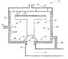
- FIG. 1depicts an exemplary embodiment chemical vapor deposition apparatus 10 usable in accordance with methodical aspects of the invention. Any other apparatus, whether existing or yet-to-be-developed, could of course also/alternatively be utilized.
- Apparatus 10includes a chamber 15 defined at least in part by chamber walls 12 , 14 and 16 .
- Wall or walls 12comprise a chamber sidewall
- wall or walls 14comprise a chamber base wall
- wall or walls 16comprise a chamber top wall.
- Chamber 15includes at least one process chemical inlet 18 thereto, and an outlet 20 feeding therefrom. Outlet 20 feeds to a foreline 22 for connection with a vacuum pump (not shown).
- a suitable substrate holder 24is provided within chamber 15 .
- Suchincludes some suitable support structure 26 , and is illustrated as receiving a substrate 25 , preferably a semiconductor substrate, thereatop.
- a substrate 25preferably a semiconductor substrate
- semiconductor substrateor “semiconductive substrate” is defined to mean any construction comprising semiconductive material, including, but not limited to, bulk semiconductive materials such as a semiconductive wafer (either alone or in assemblies comprising other materials thereon), and semiconductive material layers (either alone or in assemblies comprising other materials).
- substraterefers to any supporting structure, including, but not limited to, the semiconductive substrates described above.
- Process gas inlet 18is diagrammatically shown as feeding to a showerhead 27 associated with a lid of the apparatus for providing one or more process gasses to substrate 25 for deposition of a material thereon.
- Chamber sidewalls 12 and chamber base walls 14are depicted as having chamber surfaces having a plurality of purge gas inlets 28 to the chamber formed therein.
- the depicted purge gas inletsare separate or different from process gas inlet 18 .
- a plenum chamber 30is formed behind walls 12 , 14 and is fed by a purge gas inlet passageway 32 , which is thereby in fluid communication with purge gas inlets 28 .
- walls 12 , 14are constructed of highly porous materials, such as sintered metal particles or fibers, low density teflon, or other synthetic organic and/or inorganic materials, and by way of example only. Material selection would ideally be based on intended process chemistries.
- walls 12 , 14might be constructed to form a screen-like mesh, with pores/outlets 28 being defined by interstices thereof.
- the pore sizes of the materialwould depend on material characteristics and deposition process characteristics. Exemplary pore sizes include from tens of microns to tens of Angstroms.
- walls 12 , 14might comprise an essentially solid, hard, planar wall surface having a plurality of openings 28 drilled or otherwise formed therein, such as is shown. In FIG. 1 . the chamber surface having the plurality of purge gas inlets 28 is essentially formed on and constitutes both the chamber sidewall and the chamber base wall.
- purge gas inletsmight alternately be included only on either the sidewall or base wall, and the chamber surface can be considered as being only a portion or portions thereof. Further, purge gas inlets might also be provided on a top wall of chamber 15 , for example in manners described herein, and in accordance with U.S. patent application Ser. No. 09/805,620 filed on Mar. 13, 2001, entitled “Chemical Vapor Deposition Apparatus and Deposition Methods”, listing Craig M. Carpenter and Ross S. Dando as inventors, and which is hereby incorporated by reference.
- the purge gas inletsare substantially uniformly distributed over the chamber surface over which such are received.
- purge gas inlets 28might all be of substantially constant size, or of at least two inlet sizes.
- at least some of purge gas inlets 28 which are further from chamber outlet 20are larger than at least some of the purge gas inlets 28 which are closer to chamber outlet 20 .
- Suchprovides one manner by which, if desired, a greater volumetric flow of purge gas can be provided proximate the respective wall surfaces further from chamber outlet 20 than closer thereto.
- a purge gas outlet passageway 36is depicted as extending from purge gas inlet passageway 32 , 30 to foreline 22 , thereby by-passing the plurality of purge gas inlets 28 .
- Appropriate valvingmight, of course, be associated with passageway 36 or any other of the depicted passageways/inlets/outlets.
- a purge gas outlet passagewaymight be included to assist in control of the flow rate and pressure within plenum chamber 30 and, thereby, also from purge gas inlets 28 .
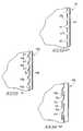
- FIGS. 2 , 3 and 4depict exemplary alternate purge gas inlets 28 .
- FIG. 2depicts an exemplary chamber wall 40 having a chamber surface 42 having a plurality of purge gas inlets 28 a received therein. Such are depicted as comprising openings extending from a purge gas inlet passageway 44 within wall 40 and which would be exposed to a deposition chamber, for example deposition chamber 15 .
- the exemplary depicted purge gas inlets 28 a in such embodimentare configured for discharging purge gas to the chamber in a direction which is substantially transverse, for example in a direction “A” to chamber surface 42 .
- a direction substantially transverseis defined to mean anything from perfectly perpendicular (90°) to the chamber surface to, but not including, 45° from the chamber surface.
- FIG. 3depicts an exemplary alternate embodiment chamber wall 40 b .
- Like numerals from the FIG. 2 described embodimentare utilized where appropriate, with differences being indicated by the suffix “b” or with different numerals.
- Purge gas inlets 28 bare depicted as being configured for discharging purge gas to the chamber in a direction substantially along chamber surface 42 b . In the context of this document, “substantially along” means from 45° to parallel with the chamber surface. In the depicted exemplary FIG.
- chamber surface 42 bis provided (or alternately considered, purge inlets 28 b are provided) with deflectors/diverters/ramps 43 angled at an exemplary 40° from surface 42 b for achieving such purge gas discharging generally in a direction “B”.
- FIG. 4depicts yet another embodiment configuration for purge gas inlets 28 c .
- deflectors 43 care depicted as curving or ramping to extend a portion thereof essentially parallel along surface 42 c.
- one preferred deposition methodpositions a substrate within a deposition chamber defined, at least in part, by chamber walls such as, by way of example only, substrate 25 positioned within chemical vapor deposition apparatus 10 .
- At least one of the chamber wallscomprises a chamber surface having a plurality of purge gas inlets to the chamber.
- any multiple set or subset of purge gas inlets 28depict such a plurality of purge gas inlets.
- a process gas(i.e., in one or more flowings) is provided over the substrate effective to deposit a layer onto the substrate.
- one or more process gassescould be provided via process gas inlet 18 to showerhead 27 .
- some materialadheres to the chamber surface.
- a reactive purge gasis emitted to the deposition chamber from purge gas inlets effective to form a reactive gas curtain over the chamber surface and away from the substrate, with such reactive gas reacting with the adhering material.
- the reactive gas flowingoccurs after depositing the layer on the substrate.
- the reactive gas flowingoccurs during the process gas flowing.
- the reactive purge gasis different in composition from all of the process gas. Further, the reactive gas may or may not be capable under conditions of the reactive gas flowing of reaction with the exposed layer which has or is being deposited.
- the adhering materialmight be reactive with one or a multiple of the deposition precursors. In such event, it might be desirable to remove such adhering material from the substrate so it will not react with subsequent flowing precursor, or at least in some way passivate such adhering material to preclude its reaction with subsequently flowing deposition precursors. Further by way of example only, the adhering material might result, in part, from the reaction of deposition precursor with material of the chamber surface, thus forming material adhering thereto. Such might constitute a monolayer in ALD including eventually considerably thicker layers from the successive formation of repeated monolayers.
- an exemplary adhered materialmight comprise oxygen atoms adhering to a metal chamber surface. Such could manifest by the feeding of ozone in any of the above-described exemplary processes involving the deposition of Al 2 O 3 . Alternately by way of example only, such might encompass any of TiCl 2 , TiCl 3 and NH 3 complexes with respect to TiCl 4 and NH 3 deposition precursor flows.
- the reactive gasreacts to modify the composition of the adhering material, with such modified composition material adhering to the chamber surface.
- the adhering materialcomprises Al—(CH 3 ) 2
- an exemplary reactive gaswould be activated hydrogen to modify the adhering material composition to Al, which still adheres to the chamber surface.
- the reactive gasreacts to effectively remove the adhered material, and any reaction by-product thereof, from adhering to the chamber surface.
- the adhering materialcomprises TiCl, TiCl 2 and/or TiCl 3
- an exemplary reactive gasincludes Cl 2 , which would effectively etch or otherwise vaporize the adhering material from the substrate and be exhausted from the chamber.
- the conditions (i.e., temperature, pressure, flow rate, etc.) of the reactive gas flowingcan be optimized by the artisan and are not otherwise particularly germane or preferred to any aspect of the invention. By way of example only, such conditions might be the same as, or different from, any of a first precursor gas flow, a second precursor gas flow and/or inert purge gas flow.
- the reactive gas flowis plasma-enhanced, for example either by plasma generation within the chamber, plasma generation remote of the chamber, or both.
- the particular reactive gas selectedwill depend as a minimum upon at least some portion or component of the adhering material which will be capable of reaction with the reactive gas under conditions of the reactive gas flowing.
- possible reactive gases componentsinclude Cl 2 , O 2 and H 2 .
- the adhering materialcomprises oxygen atoms, such might be removed in the presence of O 2 to form ozone and/or with H 2 to form H 2 O which is exhausted from the chamber.
- the reactive purge gasis emitted to the chamber in a direction substantially transverse to the chamber surface associated with the purge gas inlets and, in one embodiment, is also effective to form the reactive gas curtain to comprise substantially turbulent gas flow proximate the chamber surface.
- the purge gas emitting to the chamberis in a direction substantially along the chamber surface and, in one embodiment, is additionally effective to form the reactive gas curtain to comprise substantially laminar gas flow proximate the chamber surface. In some operating regimes, viscous or turbulent flow may be desired proximate the surface being protected, whereas in other regimes laminar flow might be desired.
- the purge gas emittingcomprises emitting a greater volume of purge gas from at least some purge gas inlets located further from the chamber outlet than from at least some purge gas inlets located closer to the chamber outlet.
- Preferred depositionsinclude chemical vapor deposition, including atomic layer deposition.
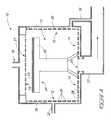
- FIG. 5depicts an exemplary alternate chemical vapor deposition apparatus 10 a .
- Chemical vapor deposition apparatus 10 aincludes a chamber liner apparatus 50 forming a deposition subchamber 17 within chamber 15 a .
- Chamber liner apparatus 50comprises subchamber surfaces 51 having a plurality of purge gas inlets 52 to the subchamber therein.
- purge gas inlets 52might be configured in any of the manners described above, including the depictions with respect to inlets 28 , 28 a , 28 b and 28 c described above.
- liner apparatus 50would ideally be configured or fabricated to be an easily replaceable component of apparatus 10 a .
- the exemplary FIG. 5 embodimentdepicts the various walls of liner apparatus 50 as comprising a retained intertwined, mesh-like material which is fed by a plurality of purge gas inlet passageways 56 for providing the desired purge gas thereto during deposition.
- Other preferred attributes of the methodfor example as described with respect to FIGS. 1-4 above, can be incorporated with chamber liner apparatus 50 .
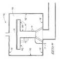
- FIG. 6depicts a chemical vapor deposition apparatus 10 f comprising a deposition chamber 15 f which is at least in part defined by chamber walls 12 f , 14 f and 16 f .
- Substrate holder 24 fcomprises support structure 26 f .
- Suchincludes a surface or surfaces 70 exposed to chamber 15 f and which comprise(s) a plurality of purge gas inlets 75 to chamber 15 f .
- An exemplary purge gas inlet passageway 77is shown in communication with support structure 26 f , and accordingly with purge gas inlets 75 .
- Such purge gas inletsmight have any of the attributes described above with respect to the other described embodiments.
- a deposition methodcomprises positioning a substrate within a deposition chamber defined at least in part by chamber walls.
- the deposition chambercomprises a component received therein internally of the chamber walls.
- substrate holder 24 f and its associated support structure 26 fis one exemplary such component.
- any other componentis contemplated in accordance with methodical aspects of the invention.
- the componentcomprises a surface, exposed to the chamber, which has a plurality of purge gas inlets to the chamber therein.
- a process gasis provided over the substrate effective to deposit a layer onto the substrate. During provision of the process gas effective to deposit a layer on the substrate, some material adheres to the chamber surface.
- a reactive purge gasis emitted to the deposition chamber from purge gas inlets effective to form a reactive gas curtain over the component surface and away from the substrate, with such reactive gas reacting with the adhering material.
- Control of the reactive purge gas flowcan be through a variety of methods, such as an active feedback control loop based on a pressure sensors ported to the purge gas channels and linked to mass flow controllers, needle valves, any of various digital valve-type flow controllers, line pressure regulators or other existing or yet-to-be developed methods.
Landscapes
- Chemical & Material Sciences (AREA)
- General Chemical & Material Sciences (AREA)
- Chemical Kinetics & Catalysis (AREA)
- Engineering & Computer Science (AREA)
- Materials Engineering (AREA)
- Mechanical Engineering (AREA)
- Metallurgy (AREA)
- Organic Chemistry (AREA)
- Chemical Vapour Deposition (AREA)
Abstract
Description
Claims (66)
Priority Applications (2)
| Application Number | Priority Date | Filing Date | Title |
|---|---|---|---|
| US10/222,304US6890596B2 (en) | 2002-08-15 | 2002-08-15 | Deposition methods |
| US11/075,017US7498057B2 (en) | 2002-08-15 | 2005-03-08 | Deposition methods |
Applications Claiming Priority (1)
| Application Number | Priority Date | Filing Date | Title |
|---|---|---|---|
| US10/222,304US6890596B2 (en) | 2002-08-15 | 2002-08-15 | Deposition methods |
Related Child Applications (1)
| Application Number | Title | Priority Date | Filing Date |
|---|---|---|---|
| US11/075,017ContinuationUS7498057B2 (en) | 2002-08-15 | 2005-03-08 | Deposition methods |
Publications (2)
| Publication Number | Publication Date |
|---|---|
| US20040033310A1 US20040033310A1 (en) | 2004-02-19 |
| US6890596B2true US6890596B2 (en) | 2005-05-10 |
Family
ID=31714929
Family Applications (2)
| Application Number | Title | Priority Date | Filing Date |
|---|---|---|---|
| US10/222,304Expired - Fee RelatedUS6890596B2 (en) | 2002-08-15 | 2002-08-15 | Deposition methods |
| US11/075,017Expired - Fee RelatedUS7498057B2 (en) | 2002-08-15 | 2005-03-08 | Deposition methods |
Family Applications After (1)
| Application Number | Title | Priority Date | Filing Date |
|---|---|---|---|
| US11/075,017Expired - Fee RelatedUS7498057B2 (en) | 2002-08-15 | 2005-03-08 | Deposition methods |
Country Status (1)
| Country | Link |
|---|---|
| US (2) | US6890596B2 (en) |
Cited By (316)
| Publication number | Priority date | Publication date | Assignee | Title |
|---|---|---|---|---|
| US20030176060A1 (en)* | 2002-03-13 | 2003-09-18 | Doan Trung Tri | Methods For Treating Pluralities Of Discrete Semiconductor Substrates |
| US20030215569A1 (en)* | 2002-05-17 | 2003-11-20 | Mardian Allen P. | Chemical vapor deposition apparatus and deposition method |
| US20040083959A1 (en)* | 2001-03-13 | 2004-05-06 | Carpenter Craig M. | Chemical vapor deposition apparatuses and deposition methods |
| US20040213908A1 (en)* | 2002-02-25 | 2004-10-28 | Derderian Garo J. | Deposition methods and apparatus for improved delivery of metastable species |
| US20040221807A1 (en)* | 2003-05-09 | 2004-11-11 | Mohith Verghese | Reactor surface passivation through chemical deactivation |
| US20050016452A1 (en)* | 2003-07-22 | 2005-01-27 | Samsung Electronics Co., Ltd. | Gas supply unit and semiconductor device manufacturing apparatus using the same |
| US20050028732A1 (en)* | 2002-01-22 | 2005-02-10 | Mardian Allen P. | Chemical vapor deposition method |
| US20050059246A1 (en)* | 2003-08-06 | 2005-03-17 | Takakazu Yamada | Device and method for manufacturing thin films |
| US20050126585A1 (en)* | 2003-12-11 | 2005-06-16 | Demetrius Sarigiannis | Method of removing residual contaminants from an environment |
| US20050147751A1 (en)* | 2002-08-15 | 2005-07-07 | Demetrius Sarigiannis | Deposition methods |
| US20050191416A1 (en)* | 2002-08-15 | 2005-09-01 | Cem Basceri | Methods of gas delivery for deposition processes and methods of depositing material on a substrate |
| US20070098894A1 (en)* | 2003-05-09 | 2007-05-03 | Mohith Verghese | Reactor surface passivation through chemical deactivation |
| US7615061B2 (en) | 2006-02-28 | 2009-11-10 | Arthrocare Corporation | Bone anchor suture-loading system, method and apparatus |
| US20100275952A1 (en)* | 2009-04-30 | 2010-11-04 | Asm America, Inc. | Selective etching of reactor surfaces |
| US20100279008A1 (en)* | 2007-09-12 | 2010-11-04 | Tokyo Electron Limited | Film deposition apparatus and film deposition method |
| US20110198736A1 (en)* | 2010-02-17 | 2011-08-18 | Asm America, Inc. | Reactive site deactivation against vapor deposition |
| US20120031337A1 (en)* | 2009-07-01 | 2012-02-09 | Ferrotec Corporation | Divided annular rib type plasma processing apparatus |
| US20130316079A1 (en)* | 2010-10-21 | 2013-11-28 | Leybold Optics Gmbh | Device and Process for Coating a Substrate |
| US20140357092A1 (en)* | 2013-06-04 | 2014-12-04 | Lam Research Corporation | Chamber wall of a plasma processing apparatus including a flowing protective liquid layer |
| US9223203B2 (en) | 2011-07-08 | 2015-12-29 | Asm International N.V. | Microcontact printed films as an activation layer for selective atomic layer deposition |
| CN106816393A (en)* | 2015-11-27 | 2017-06-09 | 中微半导体设备(上海)有限公司 | Processing method for substrate and equipment |
| US10157755B2 (en)* | 2015-10-01 | 2018-12-18 | Lam Research Corporation | Purge and pumping structures arranged beneath substrate plane to reduce defects |
| US10208380B2 (en)* | 2015-12-04 | 2019-02-19 | Applied Materials, Inc. | Advanced coating method and materials to prevent HDP-CVD chamber arcing |
| US10808310B2 (en)* | 2016-06-03 | 2020-10-20 | Applied Mateirals, Inc. | Effective and novel design for lower particle count and better wafer quality by diffusing the flow inside the chamber |
| US10847366B2 (en) | 2018-11-16 | 2020-11-24 | Asm Ip Holding B.V. | Methods for depositing a transition metal chalcogenide film on a substrate by a cyclical deposition process |
| US10844484B2 (en) | 2017-09-22 | 2020-11-24 | Asm Ip Holding B.V. | Apparatus for dispensing a vapor phase reactant to a reaction chamber and related methods |
| US10844486B2 (en) | 2009-04-06 | 2020-11-24 | Asm Ip Holding B.V. | Semiconductor processing reactor and components thereof |
| US10851456B2 (en) | 2016-04-21 | 2020-12-01 | Asm Ip Holding B.V. | Deposition of metal borides |
| US10858737B2 (en) | 2014-07-28 | 2020-12-08 | Asm Ip Holding B.V. | Showerhead assembly and components thereof |
| US10867786B2 (en) | 2018-03-30 | 2020-12-15 | Asm Ip Holding B.V. | Substrate processing method |
| US10867788B2 (en) | 2016-12-28 | 2020-12-15 | Asm Ip Holding B.V. | Method of forming a structure on a substrate |
| US10883175B2 (en)* | 2018-08-09 | 2021-01-05 | Asm Ip Holding B.V. | Vertical furnace for processing substrates and a liner for use therein |
| US10886123B2 (en) | 2017-06-02 | 2021-01-05 | Asm Ip Holding B.V. | Methods for forming low temperature semiconductor layers and related semiconductor device structures |
| US10892156B2 (en) | 2017-05-08 | 2021-01-12 | Asm Ip Holding B.V. | Methods for forming a silicon nitride film on a substrate and related semiconductor device structures |
| US10910262B2 (en) | 2017-11-16 | 2021-02-02 | Asm Ip Holding B.V. | Method of selectively depositing a capping layer structure on a semiconductor device structure |
| US10914004B2 (en) | 2018-06-29 | 2021-02-09 | Asm Ip Holding B.V. | Thin-film deposition method and manufacturing method of semiconductor device |
| US10923344B2 (en) | 2017-10-30 | 2021-02-16 | Asm Ip Holding B.V. | Methods for forming a semiconductor structure and related semiconductor structures |
| US10928731B2 (en) | 2017-09-21 | 2021-02-23 | Asm Ip Holding B.V. | Method of sequential infiltration synthesis treatment of infiltrateable material and structures and devices formed using same |
| US10934619B2 (en) | 2016-11-15 | 2021-03-02 | Asm Ip Holding B.V. | Gas supply unit and substrate processing apparatus including the gas supply unit |
| US10941490B2 (en) | 2014-10-07 | 2021-03-09 | Asm Ip Holding B.V. | Multiple temperature range susceptor, assembly, reactor and system including the susceptor, and methods of using the same |
| US10943771B2 (en) | 2016-10-26 | 2021-03-09 | Asm Ip Holding B.V. | Methods for thermally calibrating reaction chambers |
| US10950432B2 (en) | 2017-04-25 | 2021-03-16 | Asm Ip Holding B.V. | Method of depositing thin film and method of manufacturing semiconductor device |
| USD913980S1 (en) | 2018-02-01 | 2021-03-23 | Asm Ip Holding B.V. | Gas supply plate for semiconductor manufacturing apparatus |
| US10975470B2 (en) | 2018-02-23 | 2021-04-13 | Asm Ip Holding B.V. | Apparatus for detecting or monitoring for a chemical precursor in a high temperature environment |
| US11001925B2 (en) | 2016-12-19 | 2021-05-11 | Asm Ip Holding B.V. | Substrate processing apparatus |
| US11004977B2 (en) | 2017-07-19 | 2021-05-11 | Asm Ip Holding B.V. | Method for depositing a group IV semiconductor and related semiconductor device structures |
| US11018002B2 (en) | 2017-07-19 | 2021-05-25 | Asm Ip Holding B.V. | Method for selectively depositing a Group IV semiconductor and related semiconductor device structures |
| US11018047B2 (en) | 2018-01-25 | 2021-05-25 | Asm Ip Holding B.V. | Hybrid lift pin |
| US11015245B2 (en) | 2014-03-19 | 2021-05-25 | Asm Ip Holding B.V. | Gas-phase reactor and system having exhaust plenum and components thereof |
| US11024523B2 (en) | 2018-09-11 | 2021-06-01 | Asm Ip Holding B.V. | Substrate processing apparatus and method |
| US11022879B2 (en) | 2017-11-24 | 2021-06-01 | Asm Ip Holding B.V. | Method of forming an enhanced unexposed photoresist layer |
| US11031242B2 (en) | 2018-11-07 | 2021-06-08 | Asm Ip Holding B.V. | Methods for depositing a boron doped silicon germanium film |
| USD922229S1 (en) | 2019-06-05 | 2021-06-15 | Asm Ip Holding B.V. | Device for controlling a temperature of a gas supply unit |
| US11049751B2 (en) | 2018-09-14 | 2021-06-29 | Asm Ip Holding B.V. | Cassette supply system to store and handle cassettes and processing apparatus equipped therewith |
| US11053591B2 (en) | 2018-08-06 | 2021-07-06 | Asm Ip Holding B.V. | Multi-port gas injection system and reactor system including same |
| US11056567B2 (en) | 2018-05-11 | 2021-07-06 | Asm Ip Holding B.V. | Method of forming a doped metal carbide film on a substrate and related semiconductor device structures |
| US11056344B2 (en) | 2017-08-30 | 2021-07-06 | Asm Ip Holding B.V. | Layer forming method |
| US11069510B2 (en) | 2017-08-30 | 2021-07-20 | Asm Ip Holding B.V. | Substrate processing apparatus |
| US11078568B2 (en)* | 2019-01-08 | 2021-08-03 | Applied Materials, Inc. | Pumping apparatus and method for substrate processing chambers |
| US11081345B2 (en) | 2018-02-06 | 2021-08-03 | Asm Ip Holding B.V. | Method of post-deposition treatment for silicon oxide film |
| US11088002B2 (en) | 2018-03-29 | 2021-08-10 | Asm Ip Holding B.V. | Substrate rack and a substrate processing system and method |
| US11087997B2 (en) | 2018-10-31 | 2021-08-10 | Asm Ip Holding B.V. | Substrate processing apparatus for processing substrates |
| US11094546B2 (en) | 2017-10-05 | 2021-08-17 | Asm Ip Holding B.V. | Method for selectively depositing a metallic film on a substrate |
| US11094582B2 (en) | 2016-07-08 | 2021-08-17 | Asm Ip Holding B.V. | Selective deposition method to form air gaps |
| US11101370B2 (en) | 2016-05-02 | 2021-08-24 | Asm Ip Holding B.V. | Method of forming a germanium oxynitride film |
| US11107676B2 (en) | 2016-07-28 | 2021-08-31 | Asm Ip Holding B.V. | Method and apparatus for filling a gap |
| US11114283B2 (en) | 2018-03-16 | 2021-09-07 | Asm Ip Holding B.V. | Reactor, system including the reactor, and methods of manufacturing and using same |
| US11114294B2 (en) | 2019-03-08 | 2021-09-07 | Asm Ip Holding B.V. | Structure including SiOC layer and method of forming same |
| USD930782S1 (en) | 2019-08-22 | 2021-09-14 | Asm Ip Holding B.V. | Gas distributor |
| US11127617B2 (en) | 2017-11-27 | 2021-09-21 | Asm Ip Holding B.V. | Storage device for storing wafer cassettes for use with a batch furnace |
| US11127589B2 (en) | 2019-02-01 | 2021-09-21 | Asm Ip Holding B.V. | Method of topology-selective film formation of silicon oxide |
| USD931978S1 (en) | 2019-06-27 | 2021-09-28 | Asm Ip Holding B.V. | Showerhead vacuum transport |
| US11139191B2 (en) | 2017-08-09 | 2021-10-05 | Asm Ip Holding B.V. | Storage apparatus for storing cassettes for substrates and processing apparatus equipped therewith |
| US11139308B2 (en) | 2015-12-29 | 2021-10-05 | Asm Ip Holding B.V. | Atomic layer deposition of III-V compounds to form V-NAND devices |
| US11158513B2 (en) | 2018-12-13 | 2021-10-26 | Asm Ip Holding B.V. | Methods for forming a rhenium-containing film on a substrate by a cyclical deposition process and related semiconductor device structures |
| US11164955B2 (en) | 2017-07-18 | 2021-11-02 | Asm Ip Holding B.V. | Methods for forming a semiconductor device structure and related semiconductor device structures |
| USD935572S1 (en) | 2019-05-24 | 2021-11-09 | Asm Ip Holding B.V. | Gas channel plate |
| US11171025B2 (en) | 2019-01-22 | 2021-11-09 | Asm Ip Holding B.V. | Substrate processing device |
| US11168395B2 (en) | 2018-06-29 | 2021-11-09 | Asm Ip Holding B.V. | Temperature-controlled flange and reactor system including same |
| US11205585B2 (en) | 2016-07-28 | 2021-12-21 | Asm Ip Holding B.V. | Substrate processing apparatus and method of operating the same |
| US11217444B2 (en) | 2018-11-30 | 2022-01-04 | Asm Ip Holding B.V. | Method for forming an ultraviolet radiation responsive metal oxide-containing film |
| US11222772B2 (en) | 2016-12-14 | 2022-01-11 | Asm Ip Holding B.V. | Substrate processing apparatus |
| USD940837S1 (en) | 2019-08-22 | 2022-01-11 | Asm Ip Holding B.V. | Electrode |
| US11227782B2 (en) | 2019-07-31 | 2022-01-18 | Asm Ip Holding B.V. | Vertical batch furnace assembly |
| US11227789B2 (en) | 2019-02-20 | 2022-01-18 | Asm Ip Holding B.V. | Method and apparatus for filling a recess formed within a substrate surface |
| US11232963B2 (en) | 2018-10-03 | 2022-01-25 | Asm Ip Holding B.V. | Substrate processing apparatus and method |
| US11230766B2 (en) | 2018-03-29 | 2022-01-25 | Asm Ip Holding B.V. | Substrate processing apparatus and method |
| US11233133B2 (en) | 2015-10-21 | 2022-01-25 | Asm Ip Holding B.V. | NbMC layers |
| US11242598B2 (en) | 2015-06-26 | 2022-02-08 | Asm Ip Holding B.V. | Structures including metal carbide material, devices including the structures, and methods of forming same |
| US11251068B2 (en) | 2018-10-19 | 2022-02-15 | Asm Ip Holding B.V. | Substrate processing apparatus and substrate processing method |
| US11251040B2 (en) | 2019-02-20 | 2022-02-15 | Asm Ip Holding B.V. | Cyclical deposition method including treatment step and apparatus for same |
| US11251035B2 (en) | 2016-12-22 | 2022-02-15 | Asm Ip Holding B.V. | Method of forming a structure on a substrate |
| USD944946S1 (en) | 2019-06-14 | 2022-03-01 | Asm Ip Holding B.V. | Shower plate |
| US11270899B2 (en) | 2018-06-04 | 2022-03-08 | Asm Ip Holding B.V. | Wafer handling chamber with moisture reduction |
| US11274369B2 (en) | 2018-09-11 | 2022-03-15 | Asm Ip Holding B.V. | Thin film deposition method |
| US11282698B2 (en) | 2019-07-19 | 2022-03-22 | Asm Ip Holding B.V. | Method of forming topology-controlled amorphous carbon polymer film |
| US11289326B2 (en) | 2019-05-07 | 2022-03-29 | Asm Ip Holding B.V. | Method for reforming amorphous carbon polymer film |
| US11286558B2 (en) | 2019-08-23 | 2022-03-29 | Asm Ip Holding B.V. | Methods for depositing a molybdenum nitride film on a surface of a substrate by a cyclical deposition process and related semiconductor device structures including a molybdenum nitride film |
| US11286562B2 (en) | 2018-06-08 | 2022-03-29 | Asm Ip Holding B.V. | Gas-phase chemical reactor and method of using same |
| USD947913S1 (en) | 2019-05-17 | 2022-04-05 | Asm Ip Holding B.V. | Susceptor shaft |
| US11295980B2 (en) | 2017-08-30 | 2022-04-05 | Asm Ip Holding B.V. | Methods for depositing a molybdenum metal film over a dielectric surface of a substrate by a cyclical deposition process and related semiconductor device structures |
| US11296189B2 (en) | 2018-06-21 | 2022-04-05 | Asm Ip Holding B.V. | Method for depositing a phosphorus doped silicon arsenide film and related semiconductor device structures |
| USD948463S1 (en) | 2018-10-24 | 2022-04-12 | Asm Ip Holding B.V. | Susceptor for semiconductor substrate supporting apparatus |
| USD949319S1 (en) | 2019-08-22 | 2022-04-19 | Asm Ip Holding B.V. | Exhaust duct |
| US11306395B2 (en) | 2017-06-28 | 2022-04-19 | Asm Ip Holding B.V. | Methods for depositing a transition metal nitride film on a substrate by atomic layer deposition and related deposition apparatus |
| US11315794B2 (en) | 2019-10-21 | 2022-04-26 | Asm Ip Holding B.V. | Apparatus and methods for selectively etching films |
| US11339476B2 (en) | 2019-10-08 | 2022-05-24 | Asm Ip Holding B.V. | Substrate processing device having connection plates, substrate processing method |
| US11342216B2 (en) | 2019-02-20 | 2022-05-24 | Asm Ip Holding B.V. | Cyclical deposition method and apparatus for filling a recess formed within a substrate surface |
| US11345999B2 (en) | 2019-06-06 | 2022-05-31 | Asm Ip Holding B.V. | Method of using a gas-phase reactor system including analyzing exhausted gas |
| US11355338B2 (en) | 2019-05-10 | 2022-06-07 | Asm Ip Holding B.V. | Method of depositing material onto a surface and structure formed according to the method |
| US11361990B2 (en) | 2018-05-28 | 2022-06-14 | Asm Ip Holding B.V. | Substrate processing method and device manufactured by using the same |
| US11374112B2 (en) | 2017-07-19 | 2022-06-28 | Asm Ip Holding B.V. | Method for depositing a group IV semiconductor and related semiconductor device structures |
| US11378337B2 (en) | 2019-03-28 | 2022-07-05 | Asm Ip Holding B.V. | Door opener and substrate processing apparatus provided therewith |
| US11387106B2 (en) | 2018-02-14 | 2022-07-12 | Asm Ip Holding B.V. | Method for depositing a ruthenium-containing film on a substrate by a cyclical deposition process |
| US11387120B2 (en) | 2017-09-28 | 2022-07-12 | Asm Ip Holding B.V. | Chemical dispensing apparatus and methods for dispensing a chemical to a reaction chamber |
| US11393690B2 (en) | 2018-01-19 | 2022-07-19 | Asm Ip Holding B.V. | Deposition method |
| US11390946B2 (en) | 2019-01-17 | 2022-07-19 | Asm Ip Holding B.V. | Methods of forming a transition metal containing film on a substrate by a cyclical deposition process |
| US11390950B2 (en) | 2017-01-10 | 2022-07-19 | Asm Ip Holding B.V. | Reactor system and method to reduce residue buildup during a film deposition process |
| US11390945B2 (en) | 2019-07-03 | 2022-07-19 | Asm Ip Holding B.V. | Temperature control assembly for substrate processing apparatus and method of using same |
| US11398382B2 (en) | 2018-03-27 | 2022-07-26 | Asm Ip Holding B.V. | Method of forming an electrode on a substrate and a semiconductor device structure including an electrode |
| US11401605B2 (en) | 2019-11-26 | 2022-08-02 | Asm Ip Holding B.V. | Substrate processing apparatus |
| US11410851B2 (en) | 2017-02-15 | 2022-08-09 | Asm Ip Holding B.V. | Methods for forming a metallic film on a substrate by cyclical deposition and related semiconductor device structures |
| US11411088B2 (en) | 2018-11-16 | 2022-08-09 | Asm Ip Holding B.V. | Methods for forming a metal silicate film on a substrate in a reaction chamber and related semiconductor device structures |
| US11414760B2 (en) | 2018-10-08 | 2022-08-16 | Asm Ip Holding B.V. | Substrate support unit, thin film deposition apparatus including the same, and substrate processing apparatus including the same |
| US11417545B2 (en) | 2017-08-08 | 2022-08-16 | Asm Ip Holding B.V. | Radiation shield |
| US11424119B2 (en) | 2019-03-08 | 2022-08-23 | Asm Ip Holding B.V. | Method for selective deposition of silicon nitride layer and structure including selectively-deposited silicon nitride layer |
| US11430640B2 (en) | 2019-07-30 | 2022-08-30 | Asm Ip Holding B.V. | Substrate processing apparatus |
| US11430674B2 (en) | 2018-08-22 | 2022-08-30 | Asm Ip Holding B.V. | Sensor array, apparatus for dispensing a vapor phase reactant to a reaction chamber and related methods |
| US11437241B2 (en) | 2020-04-08 | 2022-09-06 | Asm Ip Holding B.V. | Apparatus and methods for selectively etching silicon oxide films |
| US11443926B2 (en) | 2019-07-30 | 2022-09-13 | Asm Ip Holding B.V. | Substrate processing apparatus |
| US11447864B2 (en) | 2019-04-19 | 2022-09-20 | Asm Ip Holding B.V. | Layer forming method and apparatus |
| US11447861B2 (en) | 2016-12-15 | 2022-09-20 | Asm Ip Holding B.V. | Sequential infiltration synthesis apparatus and a method of forming a patterned structure |
| US11453943B2 (en) | 2016-05-25 | 2022-09-27 | Asm Ip Holding B.V. | Method for forming carbon-containing silicon/metal oxide or nitride film by ALD using silicon precursor and hydrocarbon precursor |
| USD965044S1 (en) | 2019-08-19 | 2022-09-27 | Asm Ip Holding B.V. | Susceptor shaft |
| USD965524S1 (en) | 2019-08-19 | 2022-10-04 | Asm Ip Holding B.V. | Susceptor support |
| US11469098B2 (en) | 2018-05-08 | 2022-10-11 | Asm Ip Holding B.V. | Methods for depositing an oxide film on a substrate by a cyclical deposition process and related device structures |
| US11476109B2 (en) | 2019-06-11 | 2022-10-18 | Asm Ip Holding B.V. | Method of forming an electronic structure using reforming gas, system for performing the method, and structure formed using the method |
| US11473195B2 (en) | 2018-03-01 | 2022-10-18 | Asm Ip Holding B.V. | Semiconductor processing apparatus and a method for processing a substrate |
| US11482418B2 (en) | 2018-02-20 | 2022-10-25 | Asm Ip Holding B.V. | Substrate processing method and apparatus |
| US11482533B2 (en) | 2019-02-20 | 2022-10-25 | Asm Ip Holding B.V. | Apparatus and methods for plug fill deposition in 3-D NAND applications |
| US11482412B2 (en) | 2018-01-19 | 2022-10-25 | Asm Ip Holding B.V. | Method for depositing a gap-fill layer by plasma-assisted deposition |
| US11488819B2 (en) | 2018-12-04 | 2022-11-01 | Asm Ip Holding B.V. | Method of cleaning substrate processing apparatus |
| US11488854B2 (en) | 2020-03-11 | 2022-11-01 | Asm Ip Holding B.V. | Substrate handling device with adjustable joints |
| US11492703B2 (en) | 2018-06-27 | 2022-11-08 | Asm Ip Holding B.V. | Cyclic deposition methods for forming metal-containing material and films and structures including the metal-containing material |
| US11495459B2 (en) | 2019-09-04 | 2022-11-08 | Asm Ip Holding B.V. | Methods for selective deposition using a sacrificial capping layer |
| US11499222B2 (en) | 2018-06-27 | 2022-11-15 | Asm Ip Holding B.V. | Cyclic deposition methods for forming metal-containing material and films and structures including the metal-containing material |
| US11499226B2 (en) | 2018-11-02 | 2022-11-15 | Asm Ip Holding B.V. | Substrate supporting unit and a substrate processing device including the same |
| US11501973B2 (en) | 2018-01-16 | 2022-11-15 | Asm Ip Holding B.V. | Method for depositing a material film on a substrate within a reaction chamber by a cyclical deposition process and related device structures |
| US11501956B2 (en) | 2012-10-12 | 2022-11-15 | Asm Ip Holding B.V. | Semiconductor reaction chamber showerhead |
| US11501968B2 (en) | 2019-11-15 | 2022-11-15 | Asm Ip Holding B.V. | Method for providing a semiconductor device with silicon filled gaps |
| US11515187B2 (en) | 2020-05-01 | 2022-11-29 | Asm Ip Holding B.V. | Fast FOUP swapping with a FOUP handler |
| US11515188B2 (en) | 2019-05-16 | 2022-11-29 | Asm Ip Holding B.V. | Wafer boat handling device, vertical batch furnace and method |
| US11521851B2 (en) | 2020-02-03 | 2022-12-06 | Asm Ip Holding B.V. | Method of forming structures including a vanadium or indium layer |
| US11527400B2 (en) | 2019-08-23 | 2022-12-13 | Asm Ip Holding B.V. | Method for depositing silicon oxide film having improved quality by peald using bis(diethylamino)silane |
| US11527403B2 (en) | 2019-12-19 | 2022-12-13 | Asm Ip Holding B.V. | Methods for filling a gap feature on a substrate surface and related semiconductor structures |
| US11530483B2 (en) | 2018-06-21 | 2022-12-20 | Asm Ip Holding B.V. | Substrate processing system |
| US11532757B2 (en) | 2016-10-27 | 2022-12-20 | Asm Ip Holding B.V. | Deposition of charge trapping layers |
| US11530876B2 (en) | 2020-04-24 | 2022-12-20 | Asm Ip Holding B.V. | Vertical batch furnace assembly comprising a cooling gas supply |
| US11551925B2 (en) | 2019-04-01 | 2023-01-10 | Asm Ip Holding B.V. | Method for manufacturing a semiconductor device |
| US11551912B2 (en) | 2020-01-20 | 2023-01-10 | Asm Ip Holding B.V. | Method of forming thin film and method of modifying surface of thin film |
| US11557474B2 (en) | 2019-07-29 | 2023-01-17 | Asm Ip Holding B.V. | Methods for selective deposition utilizing n-type dopants and/or alternative dopants to achieve high dopant incorporation |
| USD975665S1 (en) | 2019-05-17 | 2023-01-17 | Asm Ip Holding B.V. | Susceptor shaft |
| US11562901B2 (en) | 2019-09-25 | 2023-01-24 | Asm Ip Holding B.V. | Substrate processing method |
| US11572620B2 (en) | 2018-11-06 | 2023-02-07 | Asm Ip Holding B.V. | Methods for selectively depositing an amorphous silicon film on a substrate |
| US11581186B2 (en) | 2016-12-15 | 2023-02-14 | Asm Ip Holding B.V. | Sequential infiltration synthesis apparatus |
| US11587814B2 (en) | 2019-07-31 | 2023-02-21 | Asm Ip Holding B.V. | Vertical batch furnace assembly |
| US11587821B2 (en) | 2017-08-08 | 2023-02-21 | Asm Ip Holding B.V. | Substrate lift mechanism and reactor including same |
| US11587815B2 (en) | 2019-07-31 | 2023-02-21 | Asm Ip Holding B.V. | Vertical batch furnace assembly |
| US11594600B2 (en) | 2019-11-05 | 2023-02-28 | Asm Ip Holding B.V. | Structures with doped semiconductor layers and methods and systems for forming same |
| USD979506S1 (en) | 2019-08-22 | 2023-02-28 | Asm Ip Holding B.V. | Insulator |
| US11594450B2 (en) | 2019-08-22 | 2023-02-28 | Asm Ip Holding B.V. | Method for forming a structure with a hole |
| USD980813S1 (en) | 2021-05-11 | 2023-03-14 | Asm Ip Holding B.V. | Gas flow control plate for substrate processing apparatus |
| US11605528B2 (en) | 2019-07-09 | 2023-03-14 | Asm Ip Holding B.V. | Plasma device using coaxial waveguide, and substrate treatment method |
| USD980814S1 (en) | 2021-05-11 | 2023-03-14 | Asm Ip Holding B.V. | Gas distributor for substrate processing apparatus |
| US11610775B2 (en) | 2016-07-28 | 2023-03-21 | Asm Ip Holding B.V. | Method and apparatus for filling a gap |
| US11610774B2 (en) | 2019-10-02 | 2023-03-21 | Asm Ip Holding B.V. | Methods for forming a topographically selective silicon oxide film by a cyclical plasma-enhanced deposition process |
| US11615970B2 (en) | 2019-07-17 | 2023-03-28 | Asm Ip Holding B.V. | Radical assist ignition plasma system and method |
| USD981973S1 (en) | 2021-05-11 | 2023-03-28 | Asm Ip Holding B.V. | Reactor wall for substrate processing apparatus |
| US11626316B2 (en) | 2019-11-20 | 2023-04-11 | Asm Ip Holding B.V. | Method of depositing carbon-containing material on a surface of a substrate, structure formed using the method, and system for forming the structure |
| US11626308B2 (en) | 2020-05-13 | 2023-04-11 | Asm Ip Holding B.V. | Laser alignment fixture for a reactor system |
| US11629407B2 (en) | 2019-02-22 | 2023-04-18 | Asm Ip Holding B.V. | Substrate processing apparatus and method for processing substrates |
| US11629406B2 (en) | 2018-03-09 | 2023-04-18 | Asm Ip Holding B.V. | Semiconductor processing apparatus comprising one or more pyrometers for measuring a temperature of a substrate during transfer of the substrate |
| US11637011B2 (en) | 2019-10-16 | 2023-04-25 | Asm Ip Holding B.V. | Method of topology-selective film formation of silicon oxide |
| US11637014B2 (en) | 2019-10-17 | 2023-04-25 | Asm Ip Holding B.V. | Methods for selective deposition of doped semiconductor material |
| US11639548B2 (en) | 2019-08-21 | 2023-05-02 | Asm Ip Holding B.V. | Film-forming material mixed-gas forming device and film forming device |
| US11639811B2 (en) | 2017-11-27 | 2023-05-02 | Asm Ip Holding B.V. | Apparatus including a clean mini environment |
| US11646204B2 (en) | 2020-06-24 | 2023-05-09 | Asm Ip Holding B.V. | Method for forming a layer provided with silicon |
| US11646205B2 (en) | 2019-10-29 | 2023-05-09 | Asm Ip Holding B.V. | Methods of selectively forming n-type doped material on a surface, systems for selectively forming n-type doped material, and structures formed using same |
| US11643724B2 (en) | 2019-07-18 | 2023-05-09 | Asm Ip Holding B.V. | Method of forming structures using a neutral beam |
| US11644758B2 (en) | 2020-07-17 | 2023-05-09 | Asm Ip Holding B.V. | Structures and methods for use in photolithography |
| US11646197B2 (en) | 2018-07-03 | 2023-05-09 | Asm Ip Holding B.V. | Method for depositing silicon-free carbon-containing film as gap-fill layer by pulse plasma-assisted deposition |
| US11646184B2 (en) | 2019-11-29 | 2023-05-09 | Asm Ip Holding B.V. | Substrate processing apparatus |
| US11649546B2 (en) | 2016-07-08 | 2023-05-16 | Asm Ip Holding B.V. | Organic reactants for atomic layer deposition |
| US11658030B2 (en) | 2017-03-29 | 2023-05-23 | Asm Ip Holding B.V. | Method for forming doped metal oxide films on a substrate by cyclical deposition and related semiconductor device structures |
| US11658029B2 (en) | 2018-12-14 | 2023-05-23 | Asm Ip Holding B.V. | Method of forming a device structure using selective deposition of gallium nitride and system for same |
| US11658035B2 (en) | 2020-06-30 | 2023-05-23 | Asm Ip Holding B.V. | Substrate processing method |
| US11664245B2 (en) | 2019-07-16 | 2023-05-30 | Asm Ip Holding B.V. | Substrate processing device |
| US11664199B2 (en) | 2018-10-19 | 2023-05-30 | Asm Ip Holding B.V. | Substrate processing apparatus and substrate processing method |
| US11664267B2 (en) | 2019-07-10 | 2023-05-30 | Asm Ip Holding B.V. | Substrate support assembly and substrate processing device including the same |
| US11676812B2 (en) | 2016-02-19 | 2023-06-13 | Asm Ip Holding B.V. | Method for forming silicon nitride film selectively on top/bottom portions |
| US11674220B2 (en) | 2020-07-20 | 2023-06-13 | Asm Ip Holding B.V. | Method for depositing molybdenum layers using an underlayer |
| US11680839B2 (en) | 2019-08-05 | 2023-06-20 | Asm Ip Holding B.V. | Liquid level sensor for a chemical source vessel |
| USD990441S1 (en) | 2021-09-07 | 2023-06-27 | Asm Ip Holding B.V. | Gas flow control plate |
| US11685991B2 (en) | 2018-02-14 | 2023-06-27 | Asm Ip Holding B.V. | Method for depositing a ruthenium-containing film on a substrate by a cyclical deposition process |
| USD990534S1 (en) | 2020-09-11 | 2023-06-27 | Asm Ip Holding B.V. | Weighted lift pin |
| US11688603B2 (en) | 2019-07-17 | 2023-06-27 | Asm Ip Holding B.V. | Methods of forming silicon germanium structures |
| US11705333B2 (en) | 2020-05-21 | 2023-07-18 | Asm Ip Holding B.V. | Structures including multiple carbon layers and methods of forming and using same |
| US11718913B2 (en) | 2018-06-04 | 2023-08-08 | Asm Ip Holding B.V. | Gas distribution system and reactor system including same |
| US11725277B2 (en) | 2011-07-20 | 2023-08-15 | Asm Ip Holding B.V. | Pressure transmitter for a semiconductor processing environment |
| US11725280B2 (en) | 2020-08-26 | 2023-08-15 | Asm Ip Holding B.V. | Method for forming metal silicon oxide and metal silicon oxynitride layers |
| US11735422B2 (en) | 2019-10-10 | 2023-08-22 | Asm Ip Holding B.V. | Method of forming a photoresist underlayer and structure including same |
| US11742198B2 (en) | 2019-03-08 | 2023-08-29 | Asm Ip Holding B.V. | Structure including SiOCN layer and method of forming same |
| US11742189B2 (en) | 2015-03-12 | 2023-08-29 | Asm Ip Holding B.V. | Multi-zone reactor, system including the reactor, and method of using the same |
| US11769682B2 (en) | 2017-08-09 | 2023-09-26 | Asm Ip Holding B.V. | Storage apparatus for storing cassettes for substrates and processing apparatus equipped therewith |
| US11767589B2 (en) | 2020-05-29 | 2023-09-26 | Asm Ip Holding B.V. | Substrate processing device |
| US11776846B2 (en) | 2020-02-07 | 2023-10-03 | Asm Ip Holding B.V. | Methods for depositing gap filling fluids and related systems and devices |
| US11781221B2 (en) | 2019-05-07 | 2023-10-10 | Asm Ip Holding B.V. | Chemical source vessel with dip tube |
| US11781243B2 (en) | 2020-02-17 | 2023-10-10 | Asm Ip Holding B.V. | Method for depositing low temperature phosphorous-doped silicon |
| US11802338B2 (en) | 2017-07-26 | 2023-10-31 | Asm Ip Holding B.V. | Chemical treatment, deposition and/or infiltration apparatus and method for using the same |
| US11804364B2 (en) | 2020-05-19 | 2023-10-31 | Asm Ip Holding B.V. | Substrate processing apparatus |
| US11810788B2 (en) | 2016-11-01 | 2023-11-07 | Asm Ip Holding B.V. | Methods for forming a transition metal niobium nitride film on a substrate by atomic layer deposition and related semiconductor device structures |
| US11814747B2 (en) | 2019-04-24 | 2023-11-14 | Asm Ip Holding B.V. | Gas-phase reactor system-with a reaction chamber, a solid precursor source vessel, a gas distribution system, and a flange assembly |
| US11823876B2 (en) | 2019-09-05 | 2023-11-21 | Asm Ip Holding B.V. | Substrate processing apparatus |
| US11821078B2 (en) | 2020-04-15 | 2023-11-21 | Asm Ip Holding B.V. | Method for forming precoat film and method for forming silicon-containing film |
| US11823866B2 (en) | 2020-04-02 | 2023-11-21 | Asm Ip Holding B.V. | Thin film forming method |
| US11830738B2 (en) | 2020-04-03 | 2023-11-28 | Asm Ip Holding B.V. | Method for forming barrier layer and method for manufacturing semiconductor device |
| US11827981B2 (en) | 2020-10-14 | 2023-11-28 | Asm Ip Holding B.V. | Method of depositing material on stepped structure |
| US11828707B2 (en) | 2020-02-04 | 2023-11-28 | Asm Ip Holding B.V. | Method and apparatus for transmittance measurements of large articles |
| US11830730B2 (en) | 2017-08-29 | 2023-11-28 | Asm Ip Holding B.V. | Layer forming method and apparatus |
| US11840761B2 (en) | 2019-12-04 | 2023-12-12 | Asm Ip Holding B.V. | Substrate processing apparatus |
| US11848200B2 (en) | 2017-05-08 | 2023-12-19 | Asm Ip Holding B.V. | Methods for selectively forming a silicon nitride film on a substrate and related semiconductor device structures |
| US11873557B2 (en) | 2020-10-22 | 2024-01-16 | Asm Ip Holding B.V. | Method of depositing vanadium metal |
| US11876356B2 (en) | 2020-03-11 | 2024-01-16 | Asm Ip Holding B.V. | Lockout tagout assembly and system and method of using same |
| US11885023B2 (en) | 2018-10-01 | 2024-01-30 | Asm Ip Holding B.V. | Substrate retaining apparatus, system including the apparatus, and method of using same |
| US11887857B2 (en) | 2020-04-24 | 2024-01-30 | Asm Ip Holding B.V. | Methods and systems for depositing a layer comprising vanadium, nitrogen, and a further element |
| US11885020B2 (en) | 2020-12-22 | 2024-01-30 | Asm Ip Holding B.V. | Transition metal deposition method |
| USD1012873S1 (en) | 2020-09-24 | 2024-01-30 | Asm Ip Holding B.V. | Electrode for semiconductor processing apparatus |
| US11885013B2 (en) | 2019-12-17 | 2024-01-30 | Asm Ip Holding B.V. | Method of forming vanadium nitride layer and structure including the vanadium nitride layer |
| US11891696B2 (en) | 2020-11-30 | 2024-02-06 | Asm Ip Holding B.V. | Injector configured for arrangement within a reaction chamber of a substrate processing apparatus |
| US11898243B2 (en) | 2020-04-24 | 2024-02-13 | Asm Ip Holding B.V. | Method of forming vanadium nitride-containing layer |
| US11901179B2 (en) | 2020-10-28 | 2024-02-13 | Asm Ip Holding B.V. | Method and device for depositing silicon onto substrates |
| US11915929B2 (en) | 2019-11-26 | 2024-02-27 | Asm Ip Holding B.V. | Methods for selectively forming a target film on a substrate comprising a first dielectric surface and a second metallic surface |
| US11923190B2 (en) | 2018-07-03 | 2024-03-05 | Asm Ip Holding B.V. | Method for depositing silicon-free carbon-containing film as gap-fill layer by pulse plasma-assisted deposition |
| US11923181B2 (en) | 2019-11-29 | 2024-03-05 | Asm Ip Holding B.V. | Substrate processing apparatus for minimizing the effect of a filling gas during substrate processing |
| US11929251B2 (en) | 2019-12-02 | 2024-03-12 | Asm Ip Holding B.V. | Substrate processing apparatus having electrostatic chuck and substrate processing method |
| US11946137B2 (en) | 2020-12-16 | 2024-04-02 | Asm Ip Holding B.V. | Runout and wobble measurement fixtures |
| US11961741B2 (en) | 2020-03-12 | 2024-04-16 | Asm Ip Holding B.V. | Method for fabricating layer structure having target topological profile |
| US11959168B2 (en) | 2020-04-29 | 2024-04-16 | Asm Ip Holding B.V. | Solid source precursor vessel |
| USD1023959S1 (en) | 2021-05-11 | 2024-04-23 | Asm Ip Holding B.V. | Electrode for substrate processing apparatus |
| US11967488B2 (en) | 2013-02-01 | 2024-04-23 | Asm Ip Holding B.V. | Method for treatment of deposition reactor |
| US11976359B2 (en) | 2020-01-06 | 2024-05-07 | Asm Ip Holding B.V. | Gas supply assembly, components thereof, and reactor system including same |
| US11986868B2 (en) | 2020-02-28 | 2024-05-21 | Asm Ip Holding B.V. | System dedicated for parts cleaning |
| US11987881B2 (en) | 2020-05-22 | 2024-05-21 | Asm Ip Holding B.V. | Apparatus for depositing thin films using hydrogen peroxide |
| US11993847B2 (en) | 2020-01-08 | 2024-05-28 | Asm Ip Holding B.V. | Injector |
| US11996289B2 (en) | 2020-04-16 | 2024-05-28 | Asm Ip Holding B.V. | Methods of forming structures including silicon germanium and silicon layers, devices formed using the methods, and systems for performing the methods |
| US11993843B2 (en) | 2017-08-31 | 2024-05-28 | Asm Ip Holding B.V. | Substrate processing apparatus |
| US11996292B2 (en) | 2019-10-25 | 2024-05-28 | Asm Ip Holding B.V. | Methods for filling a gap feature on a substrate surface and related semiconductor structures |
| US11996309B2 (en) | 2019-05-16 | 2024-05-28 | Asm Ip Holding B.V. | Wafer boat handling device, vertical batch furnace and method |
| US12009241B2 (en) | 2019-10-14 | 2024-06-11 | Asm Ip Holding B.V. | Vertical batch furnace assembly with detector to detect cassette |
| US12009224B2 (en) | 2020-09-29 | 2024-06-11 | Asm Ip Holding B.V. | Apparatus and method for etching metal nitrides |
| US12006572B2 (en) | 2019-10-08 | 2024-06-11 | Asm Ip Holding B.V. | Reactor system including a gas distribution assembly for use with activated species and method of using same |
| US12020934B2 (en) | 2020-07-08 | 2024-06-25 | Asm Ip Holding B.V. | Substrate processing method |
| US12025484B2 (en) | 2018-05-08 | 2024-07-02 | Asm Ip Holding B.V. | Thin film forming method |
| US12027365B2 (en) | 2020-11-24 | 2024-07-02 | Asm Ip Holding B.V. | Methods for filling a gap and related systems and devices |
| US12033885B2 (en) | 2020-01-06 | 2024-07-09 | Asm Ip Holding B.V. | Channeled lift pin |
| US12040200B2 (en) | 2017-06-20 | 2024-07-16 | Asm Ip Holding B.V. | Semiconductor processing apparatus and methods for calibrating a semiconductor processing apparatus |
| US12040177B2 (en) | 2020-08-18 | 2024-07-16 | Asm Ip Holding B.V. | Methods for forming a laminate film by cyclical plasma-enhanced deposition processes |
| US12040199B2 (en) | 2018-11-28 | 2024-07-16 | Asm Ip Holding B.V. | Substrate processing apparatus for processing substrates |
| US12051602B2 (en) | 2020-05-04 | 2024-07-30 | Asm Ip Holding B.V. | Substrate processing system for processing substrates with an electronics module located behind a door in a front wall of the substrate processing system |
| US12051567B2 (en) | 2020-10-07 | 2024-07-30 | Asm Ip Holding B.V. | Gas supply unit and substrate processing apparatus including gas supply unit |
| US12057314B2 (en) | 2020-05-15 | 2024-08-06 | Asm Ip Holding B.V. | Methods for silicon germanium uniformity control using multiple precursors |
| US12074022B2 (en) | 2020-08-27 | 2024-08-27 | Asm Ip Holding B.V. | Method and system for forming patterned structures using multiple patterning process |
| US12087586B2 (en) | 2020-04-15 | 2024-09-10 | Asm Ip Holding B.V. | Method of forming chromium nitride layer and structure including the chromium nitride layer |
| US12107005B2 (en) | 2020-10-06 | 2024-10-01 | Asm Ip Holding B.V. | Deposition method and an apparatus for depositing a silicon-containing material |
| US12106944B2 (en) | 2020-06-02 | 2024-10-01 | Asm Ip Holding B.V. | Rotating substrate support |
| US12112940B2 (en) | 2019-07-19 | 2024-10-08 | Asm Ip Holding B.V. | Method of forming topology-controlled amorphous carbon polymer film |
| US12125700B2 (en) | 2020-01-16 | 2024-10-22 | Asm Ip Holding B.V. | Method of forming high aspect ratio features |
| US12129545B2 (en) | 2020-12-22 | 2024-10-29 | Asm Ip Holding B.V. | Precursor capsule, a vessel and a method |
| US12131885B2 (en) | 2020-12-22 | 2024-10-29 | Asm Ip Holding B.V. | Plasma treatment device having matching box |
| US12148609B2 (en) | 2020-09-16 | 2024-11-19 | Asm Ip Holding B.V. | Silicon oxide deposition method |
| US12154824B2 (en) | 2020-08-14 | 2024-11-26 | Asm Ip Holding B.V. | Substrate processing method |
| US12159788B2 (en) | 2020-12-14 | 2024-12-03 | Asm Ip Holding B.V. | Method of forming structures for threshold voltage control |
| US12169361B2 (en) | 2019-07-30 | 2024-12-17 | Asm Ip Holding B.V. | Substrate processing apparatus and method |
| US12173404B2 (en) | 2020-03-17 | 2024-12-24 | Asm Ip Holding B.V. | Method of depositing epitaxial material, structure formed using the method, and system for performing the method |
| US12173402B2 (en) | 2018-02-15 | 2024-12-24 | Asm Ip Holding B.V. | Method of forming a transition metal containing film on a substrate by a cyclical deposition process, a method for supplying a transition metal halide compound to a reaction chamber, and related vapor deposition apparatus |
| US12195852B2 (en) | 2020-11-23 | 2025-01-14 | Asm Ip Holding B.V. | Substrate processing apparatus with an injector |
| US12209308B2 (en) | 2020-11-12 | 2025-01-28 | Asm Ip Holding B.V. | Reactor and related methods |
| US12211742B2 (en) | 2020-09-10 | 2025-01-28 | Asm Ip Holding B.V. | Methods for depositing gap filling fluid |
| US12217954B2 (en) | 2020-08-25 | 2025-02-04 | Asm Ip Holding B.V. | Method of cleaning a surface |
| USD1060598S1 (en) | 2021-12-03 | 2025-02-04 | Asm Ip Holding B.V. | Split showerhead cover |
| US12218269B2 (en) | 2020-02-13 | 2025-02-04 | Asm Ip Holding B.V. | Substrate processing apparatus including light receiving device and calibration method of light receiving device |
| US12218000B2 (en) | 2020-09-25 | 2025-02-04 | Asm Ip Holding B.V. | Semiconductor processing method |
| US12217946B2 (en) | 2020-10-15 | 2025-02-04 | Asm Ip Holding B.V. | Method of manufacturing semiconductor device, and substrate treatment apparatus using ether-CAT |
| US12221357B2 (en) | 2020-04-24 | 2025-02-11 | Asm Ip Holding B.V. | Methods and apparatus for stabilizing vanadium compounds |
| US12230531B2 (en) | 2018-04-09 | 2025-02-18 | Asm Ip Holding B.V. | Substrate supporting apparatus, substrate processing apparatus including the same, and substrate processing method |
| US12243757B2 (en) | 2020-05-21 | 2025-03-04 | Asm Ip Holding B.V. | Flange and apparatus for processing substrates |
| US12241158B2 (en) | 2020-07-20 | 2025-03-04 | Asm Ip Holding B.V. | Method for forming structures including transition metal layers |
| US12243747B2 (en) | 2020-04-24 | 2025-03-04 | Asm Ip Holding B.V. | Methods of forming structures including vanadium boride and vanadium phosphide layers |
| US12243742B2 (en) | 2020-04-21 | 2025-03-04 | Asm Ip Holding B.V. | Method for processing a substrate |
| US12240760B2 (en) | 2016-03-18 | 2025-03-04 | Asm Ip Holding B.V. | Aligned carbon nanotubes |
| US12247286B2 (en) | 2019-08-09 | 2025-03-11 | Asm Ip Holding B.V. | Heater assembly including cooling apparatus and method of using same |
| US12252785B2 (en) | 2019-06-10 | 2025-03-18 | Asm Ip Holding B.V. | Method for cleaning quartz epitaxial chambers |
| US12255053B2 (en) | 2020-12-10 | 2025-03-18 | Asm Ip Holding B.V. | Methods and systems for depositing a layer |
| US12266524B2 (en) | 2020-06-16 | 2025-04-01 | Asm Ip Holding B.V. | Method for depositing boron containing silicon germanium layers |
| US12272527B2 (en) | 2018-05-09 | 2025-04-08 | Asm Ip Holding B.V. | Apparatus for use with hydrogen radicals and method of using same |
| US12276023B2 (en) | 2017-08-04 | 2025-04-15 | Asm Ip Holding B.V. | Showerhead assembly for distributing a gas within a reaction chamber |
| US12278129B2 (en) | 2020-03-04 | 2025-04-15 | Asm Ip Holding B.V. | Alignment fixture for a reactor system |
| US12288710B2 (en) | 2020-12-18 | 2025-04-29 | Asm Ip Holding B.V. | Wafer processing apparatus with a rotatable table |
| US12322591B2 (en) | 2020-07-27 | 2025-06-03 | Asm Ip Holding B.V. | Thin film deposition process |
| US12378665B2 (en) | 2018-10-26 | 2025-08-05 | Asm Ip Holding B.V. | High temperature coatings for a preclean and etch apparatus and related methods |
| US12406846B2 (en) | 2020-05-26 | 2025-09-02 | Asm Ip Holding B.V. | Method for depositing boron and gallium containing silicon germanium layers |
| US12410515B2 (en) | 2020-01-29 | 2025-09-09 | Asm Ip Holding B.V. | Contaminant trap system for a reactor system |
| US12431354B2 (en) | 2020-07-01 | 2025-09-30 | Asm Ip Holding B.V. | Silicon nitride and silicon oxide deposition methods using fluorine inhibitor |
| US12431334B2 (en) | 2020-02-13 | 2025-09-30 | Asm Ip Holding B.V. | Gas distribution assembly |
| US12428726B2 (en) | 2019-10-08 | 2025-09-30 | Asm Ip Holding B.V. | Gas injection system and reactor system including same |
| US12442082B2 (en) | 2021-05-04 | 2025-10-14 | Asm Ip Holding B.V. | Reactor system comprising a tuning circuit |
Families Citing this family (10)
| Publication number | Priority date | Publication date | Assignee | Title |
|---|---|---|---|---|
| DE10320597A1 (en)* | 2003-04-30 | 2004-12-02 | Aixtron Ag | Method and device for depositing semiconductor layers with two process gases, one of which is preconditioned |
| DE102005032711A1 (en)* | 2005-07-07 | 2007-01-11 | Siemens Ag | Method for producing a nanoparticle-containing layer on a substrate |
| US20110237051A1 (en) | 2010-03-26 | 2011-09-29 | Kenneth Lee Hess | Process and apparatus for deposition of multicomponent semiconductor layers |
| US9937536B2 (en)* | 2012-07-12 | 2018-04-10 | Taiwan Semiconductor Manufacturing Company Limited | Air purge cleaning for semiconductor polishing apparatus |
| WO2014094103A1 (en) | 2012-12-18 | 2014-06-26 | Seastar Chemicals Inc. | Process and method for in-situ dry cleaning of thin film deposition reactors and thin film layers |
| US9738977B1 (en)* | 2016-06-17 | 2017-08-22 | Lam Research Corporation | Showerhead curtain gas method and system for film profile modulation |
| DE102017116650B4 (en)* | 2017-07-24 | 2025-03-13 | VON ARDENNE Asset GmbH & Co. KG | Processing arrangement and method for conditioning a processing arrangement |
| SG11202112556XA (en)* | 2019-05-15 | 2021-12-30 | Applied Materials Inc | Methods of reducing chamber residues |
| US12087573B2 (en) | 2019-07-17 | 2024-09-10 | Lam Research Corporation | Modulation of oxidation profile for substrate processing |
| US11427910B2 (en)* | 2020-10-20 | 2022-08-30 | Sky Tech Inc. | Atomic layer deposition equipment capable of reducing precursor deposition and atomic layer deposition process method using the same |
Citations (41)
| Publication number | Priority date | Publication date | Assignee | Title |
|---|---|---|---|---|
| US5879459A (en) | 1997-08-29 | 1999-03-09 | Genus, Inc. | Vertically-stacked process reactor and cluster tool system for atomic layer deposition |
| US5925411A (en)* | 1990-07-16 | 1999-07-20 | Siliconix Incorporated | Gas-based substrate deposition protection |
| US5972430A (en) | 1997-11-26 | 1999-10-26 | Advanced Technology Materials, Inc. | Digital chemical vapor deposition (CVD) method for forming a multi-component oxide layer |
| US6015597A (en) | 1997-11-26 | 2000-01-18 | 3M Innovative Properties Company | Method for coating diamond-like networks onto particles |
| US6174377B1 (en) | 1997-03-03 | 2001-01-16 | Genus, Inc. | Processing chamber for atomic layer deposition processes |
| US6200893B1 (en) | 1999-03-11 | 2001-03-13 | Genus, Inc | Radical-assisted sequential CVD |
| WO2001027347A1 (en) | 1999-10-15 | 2001-04-19 | Asm Microchemistry Oy | Method of depositing transition metal nitride thin films |
| WO2001029893A1 (en) | 1999-10-15 | 2001-04-26 | Asm America, Inc. | Method for depositing nanolaminate thin films on sensitive surfaces |
| WO2001029280A1 (en) | 1999-10-15 | 2001-04-26 | Asm America, Inc. | Deposition of transition metal carbides |
| US6270572B1 (en) | 1998-08-07 | 2001-08-07 | Samsung Electronics Co., Ltd. | Method for manufacturing thin film using atomic layer deposition |
| US6287965B1 (en) | 1997-07-28 | 2001-09-11 | Samsung Electronics Co, Ltd. | Method of forming metal layer using atomic layer deposition and semiconductor device having the metal layer as barrier metal layer or upper or lower electrode of capacitor |
| WO2001066832A2 (en) | 2000-03-07 | 2001-09-13 | Asm America, Inc. | Graded thin films |
| US20010024387A1 (en) | 1999-12-03 | 2001-09-27 | Ivo Raaijmakers | Conformal thin films over textured capacitor electrodes |
| US6301434B1 (en)* | 1998-03-23 | 2001-10-09 | Mattson Technology, Inc. | Apparatus and method for CVD and thermal processing of semiconductor substrates |
| US6305314B1 (en) | 1999-03-11 | 2001-10-23 | Genvs, Inc. | Apparatus and concept for minimizing parasitic chemical vapor deposition during atomic layer deposition |
| US20010050039A1 (en) | 2000-06-07 | 2001-12-13 | Park Chang-Soo | Method of forming a thin film using atomic layer deposition method |
| US20010054381A1 (en)* | 1998-12-14 | 2001-12-27 | Salvador P Umotoy | High temperature chemical vapor deposition chamber |
| US6355561B1 (en) | 2000-11-21 | 2002-03-12 | Micron Technology, Inc. | ALD method to improve surface coverage |
| US6391785B1 (en) | 1999-08-24 | 2002-05-21 | Interuniversitair Microelektronica Centrum (Imec) | Method for bottomless deposition of barrier layers in integrated circuit metallization schemes |
| US6403156B2 (en) | 2000-06-28 | 2002-06-11 | Hyundai Electronics Industries Co., Ltd. | Method of forming an A1203 film in a semiconductor device |
| US20020086111A1 (en) | 2001-01-03 | 2002-07-04 | Byun Jeong Soo | Method of forming refractory metal nitride layers using chemisorption techniques |
| US6426307B2 (en) | 2000-06-20 | 2002-07-30 | Hyundai Electronics Industries Co. | Method of manufacturing an aluminum oxide film in a semiconductor device |
| US6468924B2 (en) | 2000-12-06 | 2002-10-22 | Samsung Electronics Co., Ltd. | Methods of forming thin films by atomic layer deposition |
| US6475276B1 (en) | 1999-10-15 | 2002-11-05 | Asm Microchemistry Oy | Production of elemental thin films using a boron-containing reducing agent |
| US6475286B1 (en)* | 1999-07-13 | 2002-11-05 | Aixtron Aktiengesellschaft | Seal means for separable closing elements, such as separable elements of chemical vapor deposition chamber and deposition reactor apparatus |
| US6482476B1 (en) | 1997-10-06 | 2002-11-19 | Shengzhong Frank Liu | Low temperature plasma enhanced CVD ceramic coating process for metal, alloy and ceramic materials |
| US20030085424A1 (en) | 2001-11-02 | 2003-05-08 | International Business Machines Corporation | Transistor structure with thick recessed source/drain structures and fabrication process of same |
| US6585823B1 (en) | 2000-07-07 | 2003-07-01 | Asm International, N.V. | Atomic layer deposition |
| US6586343B1 (en)* | 1999-07-09 | 2003-07-01 | Applied Materials, Inc. | Method and apparatus for directing constituents through a processing chamber |
| US6590251B2 (en) | 1999-12-08 | 2003-07-08 | Samsung Electronics Co., Ltd. | Semiconductor devices having metal layers as barrier layers on upper or lower electrodes of capacitors |
| US6589886B2 (en) | 1999-12-22 | 2003-07-08 | Hyundai Electronics Industries Co., Ltd. | Method for manufacturing aluminum oxide film for use in a semiconductor device |
| US20030143328A1 (en) | 2002-01-26 | 2003-07-31 | Applied Materials, Inc. | Apparatus and method for plasma assisted deposition |
| US6620723B1 (en) | 2000-06-27 | 2003-09-16 | Applied Materials, Inc. | Formation of boride barrier layers using chemisorption techniques |
| US20030183171A1 (en) | 1999-03-11 | 2003-10-02 | Ofer Sneh | Apparatus and concept for minimizing parasitic chemical vapor deposition during atomic layer deposition |
| US20040033688A1 (en) | 2002-08-15 | 2004-02-19 | Demetrius Sarigiannis | Atomic layer deposition methods |
| US6696157B1 (en) | 2000-03-05 | 2004-02-24 | 3M Innovative Properties Company | Diamond-like glass thin films |
| US6696368B2 (en) | 2001-07-31 | 2004-02-24 | Micron Technology, Inc. | Titanium boronitride layer for high aspect ratio semiconductor devices |
| US6720027B2 (en) | 2002-04-08 | 2004-04-13 | Applied Materials, Inc. | Cyclical deposition of a variable content titanium silicon nitride layer |
| US6727169B1 (en) | 1999-10-15 | 2004-04-27 | Asm International, N.V. | Method of making conformal lining layers for damascene metallization |
| US6746952B2 (en) | 2001-08-29 | 2004-06-08 | Micron Technology, Inc. | Diffusion barrier layer for semiconductor wafer fabrication |
| US20040137728A1 (en) | 2002-09-13 | 2004-07-15 | Shipley Company, L.L.C. | Air gap formation |
Family Cites Families (23)
| Publication number | Priority date | Publication date | Assignee | Title |
|---|---|---|---|---|
| US5225032A (en) | 1991-08-09 | 1993-07-06 | Allied-Signal Inc. | Method of producing stoichiometric, epitaxial, monocrystalline films of silicon carbide at temperatures below 900 degrees centigrade |
| KR100333237B1 (en)* | 1993-10-29 | 2002-09-12 | 어플라이드 머티어리얼스, 인코포레이티드 | Contaminant reduction improvements for plasma etch chambers |
| JPH08302474A (en)* | 1995-04-28 | 1996-11-19 | Anelva Corp | Heating equipment for CVD equipment |
| US6258170B1 (en)* | 1997-09-11 | 2001-07-10 | Applied Materials, Inc. | Vaporization and deposition apparatus |
| US6206973B1 (en)* | 1999-04-23 | 2001-03-27 | Silicon Valley Group Thermal System Llc | Chemical vapor deposition system and method |
| FI117978B (en) | 2000-04-14 | 2007-05-15 | Asm Int | Method and apparatus for constructing a thin film on a substrate |
| US6613695B2 (en) | 2000-11-24 | 2003-09-02 | Asm America, Inc. | Surface preparation prior to deposition |
| US6613656B2 (en) | 2001-02-13 | 2003-09-02 | Micron Technology, Inc. | Sequential pulse deposition |
| US7378127B2 (en) | 2001-03-13 | 2008-05-27 | Micron Technology, Inc. | Chemical vapor deposition methods |
| US6610169B2 (en) | 2001-04-21 | 2003-08-26 | Simplus Systems Corporation | Semiconductor processing system and method |
| KR100406534B1 (en) | 2001-05-03 | 2003-11-20 | 주식회사 하이닉스반도체 | Method for fabricating ruthenium thin film |
| US6629853B2 (en) | 2001-05-17 | 2003-10-07 | Tyco Electronics Corporation | Self-aligning power connector system |
| JP4387190B2 (en)* | 2001-10-18 | 2009-12-16 | ビュン,チュル,スー | Chemical vapor deposition method and apparatus having functions of preventing contamination and increasing film growth rate |
| US7081271B2 (en) | 2001-12-07 | 2006-07-25 | Applied Materials, Inc. | Cyclical deposition of refractory metal silicon nitride |
| US7229666B2 (en)* | 2002-01-22 | 2007-06-12 | Micron Technology, Inc. | Chemical vapor deposition method |
| US6730367B2 (en) | 2002-03-05 | 2004-05-04 | Micron Technology, Inc. | Atomic layer deposition method with point of use generated reactive gas species |
| US6613587B1 (en) | 2002-04-11 | 2003-09-02 | Micron Technology, Inc. | Method of replacing at least a portion of a semiconductor substrate deposition chamber liner |
| US6620253B1 (en) | 2002-04-11 | 2003-09-16 | Micron Technology, Inc. | Engagement mechanism for semiconductor substrate deposition process kit hardware |
| US6821347B2 (en) | 2002-07-08 | 2004-11-23 | Micron Technology, Inc. | Apparatus and method for depositing materials onto microelectronic workpieces |
| US7150789B2 (en) | 2002-07-29 | 2006-12-19 | Micron Technology, Inc. | Atomic layer deposition methods |
| US6890596B2 (en)* | 2002-08-15 | 2005-05-10 | Micron Technology, Inc. | Deposition methods |
| US6673701B1 (en) | 2002-08-27 | 2004-01-06 | Micron Technology, Inc. | Atomic layer deposition methods |
| US7107998B2 (en)* | 2003-10-16 | 2006-09-19 | Novellus Systems, Inc. | Method for preventing and cleaning ruthenium-containing deposits in a CVD apparatus |
- 2002
- 2002-08-15USUS10/222,304patent/US6890596B2/ennot_activeExpired - Fee Related
- 2005
- 2005-03-08USUS11/075,017patent/US7498057B2/ennot_activeExpired - Fee Related
Patent Citations (58)
| Publication number | Priority date | Publication date | Assignee | Title |
|---|---|---|---|---|
| US6482262B1 (en) | 1959-10-10 | 2002-11-19 | Asm Microchemistry Oy | Deposition of transition metal carbides |
| US5925411A (en)* | 1990-07-16 | 1999-07-20 | Siliconix Incorporated | Gas-based substrate deposition protection |
| US6387185B2 (en) | 1997-03-03 | 2002-05-14 | Genus, Inc. | Processing chamber for atomic layer deposition processes |
| US6174377B1 (en) | 1997-03-03 | 2001-01-16 | Genus, Inc. | Processing chamber for atomic layer deposition processes |
| US20020108714A1 (en) | 1997-03-03 | 2002-08-15 | Kenneth Doering | Processing chamber for atomic layer deposition processes |
| US6287965B1 (en) | 1997-07-28 | 2001-09-11 | Samsung Electronics Co, Ltd. | Method of forming metal layer using atomic layer deposition and semiconductor device having the metal layer as barrier metal layer or upper or lower electrode of capacitor |
| US5879459A (en) | 1997-08-29 | 1999-03-09 | Genus, Inc. | Vertically-stacked process reactor and cluster tool system for atomic layer deposition |
| US6482476B1 (en) | 1997-10-06 | 2002-11-19 | Shengzhong Frank Liu | Low temperature plasma enhanced CVD ceramic coating process for metal, alloy and ceramic materials |
| US6197120B1 (en) | 1997-11-26 | 2001-03-06 | 3M Innovative Properties Company | Apparatus for coating diamond-like networks onto particles |
| US6015597A (en) | 1997-11-26 | 2000-01-18 | 3M Innovative Properties Company | Method for coating diamond-like networks onto particles |
| US5972430A (en) | 1997-11-26 | 1999-10-26 | Advanced Technology Materials, Inc. | Digital chemical vapor deposition (CVD) method for forming a multi-component oxide layer |
| US6301434B1 (en)* | 1998-03-23 | 2001-10-09 | Mattson Technology, Inc. | Apparatus and method for CVD and thermal processing of semiconductor substrates |
| US6270572B1 (en) | 1998-08-07 | 2001-08-07 | Samsung Electronics Co., Ltd. | Method for manufacturing thin film using atomic layer deposition |
| US20010054381A1 (en)* | 1998-12-14 | 2001-12-27 | Salvador P Umotoy | High temperature chemical vapor deposition chamber |
| US6475910B1 (en) | 1999-03-11 | 2002-11-05 | Genus, Inc. | Radical-assisted sequential CVD |
| US6451695B2 (en) | 1999-03-11 | 2002-09-17 | Genus, Inc. | Radical-assisted sequential CVD |
| US6638862B2 (en) | 1999-03-11 | 2003-10-28 | Genus, Inc. | Radical-assisted sequential CVD |
| US6630401B2 (en) | 1999-03-11 | 2003-10-07 | Genus, Inc. | Radical-assisted sequential CVD |
| US20030183171A1 (en) | 1999-03-11 | 2003-10-02 | Ofer Sneh | Apparatus and concept for minimizing parasitic chemical vapor deposition during atomic layer deposition |
| US6602784B2 (en) | 1999-03-11 | 2003-08-05 | Genus, Inc. | Radical-assisted sequential CVD |
| US6200893B1 (en) | 1999-03-11 | 2001-03-13 | Genus, Inc | Radical-assisted sequential CVD |
| US6305314B1 (en) | 1999-03-11 | 2001-10-23 | Genvs, Inc. | Apparatus and concept for minimizing parasitic chemical vapor deposition during atomic layer deposition |
| US6451119B2 (en) | 1999-03-11 | 2002-09-17 | Genus, Inc. | Apparatus and concept for minimizing parasitic chemical vapor deposition during atomic layer deposition |
| US6586343B1 (en)* | 1999-07-09 | 2003-07-01 | Applied Materials, Inc. | Method and apparatus for directing constituents through a processing chamber |
| US6475286B1 (en)* | 1999-07-13 | 2002-11-05 | Aixtron Aktiengesellschaft | Seal means for separable closing elements, such as separable elements of chemical vapor deposition chamber and deposition reactor apparatus |
| US6664192B2 (en) | 1999-08-24 | 2003-12-16 | Interuniversitair Microelektronica Centrum (Imec) | Method for bottomless deposition of barrier layers in integrated circuit metallization schemes |
| US6391785B1 (en) | 1999-08-24 | 2002-05-21 | Interuniversitair Microelektronica Centrum (Imec) | Method for bottomless deposition of barrier layers in integrated circuit metallization schemes |
| WO2001029280A1 (en) | 1999-10-15 | 2001-04-26 | Asm America, Inc. | Deposition of transition metal carbides |
| WO2001029893A1 (en) | 1999-10-15 | 2001-04-26 | Asm America, Inc. | Method for depositing nanolaminate thin films on sensitive surfaces |
| US6475276B1 (en) | 1999-10-15 | 2002-11-05 | Asm Microchemistry Oy | Production of elemental thin films using a boron-containing reducing agent |
| US6727169B1 (en) | 1999-10-15 | 2004-04-27 | Asm International, N.V. | Method of making conformal lining layers for damascene metallization |
| WO2001027347A1 (en) | 1999-10-15 | 2001-04-19 | Asm Microchemistry Oy | Method of depositing transition metal nitride thin films |
| US20020187256A1 (en) | 1999-10-15 | 2002-12-12 | Kai-Erik Elers | Method of producing elemental thin films |
| US20030031807A1 (en) | 1999-10-15 | 2003-02-13 | Kai-Erik Elers | Deposition of transition metal carbides |
| US20010024387A1 (en) | 1999-12-03 | 2001-09-27 | Ivo Raaijmakers | Conformal thin films over textured capacitor electrodes |
| US6590251B2 (en) | 1999-12-08 | 2003-07-08 | Samsung Electronics Co., Ltd. | Semiconductor devices having metal layers as barrier layers on upper or lower electrodes of capacitors |
| US6589886B2 (en) | 1999-12-22 | 2003-07-08 | Hyundai Electronics Industries Co., Ltd. | Method for manufacturing aluminum oxide film for use in a semiconductor device |
| US6696157B1 (en) | 2000-03-05 | 2004-02-24 | 3M Innovative Properties Company | Diamond-like glass thin films |
| US20030032281A1 (en) | 2000-03-07 | 2003-02-13 | Werkhoven Christiaan J. | Graded thin films |
| US6534395B2 (en) | 2000-03-07 | 2003-03-18 | Asm Microchemistry Oy | Method of forming graded thin films using alternating pulses of vapor phase reactants |
| US20030129826A1 (en) | 2000-03-07 | 2003-07-10 | Werkhoven Christiaan J. | Graded thin films |
| US20010041250A1 (en) | 2000-03-07 | 2001-11-15 | Werkhoven Christian J. | Graded thin films |
| WO2001066832A2 (en) | 2000-03-07 | 2001-09-13 | Asm America, Inc. | Graded thin films |
| US20010050039A1 (en) | 2000-06-07 | 2001-12-13 | Park Chang-Soo | Method of forming a thin film using atomic layer deposition method |
| US6426307B2 (en) | 2000-06-20 | 2002-07-30 | Hyundai Electronics Industries Co. | Method of manufacturing an aluminum oxide film in a semiconductor device |
| US6620723B1 (en) | 2000-06-27 | 2003-09-16 | Applied Materials, Inc. | Formation of boride barrier layers using chemisorption techniques |
| US6403156B2 (en) | 2000-06-28 | 2002-06-11 | Hyundai Electronics Industries Co., Ltd. | Method of forming an A1203 film in a semiconductor device |
| US6585823B1 (en) | 2000-07-07 | 2003-07-01 | Asm International, N.V. | Atomic layer deposition |
| US6355561B1 (en) | 2000-11-21 | 2002-03-12 | Micron Technology, Inc. | ALD method to improve surface coverage |
| US6468924B2 (en) | 2000-12-06 | 2002-10-22 | Samsung Electronics Co., Ltd. | Methods of forming thin films by atomic layer deposition |
| US20020086111A1 (en) | 2001-01-03 | 2002-07-04 | Byun Jeong Soo | Method of forming refractory metal nitride layers using chemisorption techniques |
| US6696368B2 (en) | 2001-07-31 | 2004-02-24 | Micron Technology, Inc. | Titanium boronitride layer for high aspect ratio semiconductor devices |
| US6746952B2 (en) | 2001-08-29 | 2004-06-08 | Micron Technology, Inc. | Diffusion barrier layer for semiconductor wafer fabrication |
| US20030085424A1 (en) | 2001-11-02 | 2003-05-08 | International Business Machines Corporation | Transistor structure with thick recessed source/drain structures and fabrication process of same |
| US20030143328A1 (en) | 2002-01-26 | 2003-07-31 | Applied Materials, Inc. | Apparatus and method for plasma assisted deposition |
| US6720027B2 (en) | 2002-04-08 | 2004-04-13 | Applied Materials, Inc. | Cyclical deposition of a variable content titanium silicon nitride layer |
| US20040033688A1 (en) | 2002-08-15 | 2004-02-19 | Demetrius Sarigiannis | Atomic layer deposition methods |
| US20040137728A1 (en) | 2002-09-13 | 2004-07-15 | Shipley Company, L.L.C. | Air gap formation |
Non-Patent Citations (9)
| Title |
|---|
| U.S. Appl. No. 10/121,302, Carpenter, filed Apr. 11, 2002. |
| U.S. Appl. No. 10/132,003, Dando et al., filed Apr. 24, 2002. |
| U.S. Appl. No. 10/132,767, Dando et al., filed Apr. 24, 2002. |
| U.S. Appl. No. 10/150,388, Mardian et al., filed May 17, 2002. |
| U.S. Appl. No. 10/163,671, Dando et al., filed Jun. 5, 2002. |
| U.S. Appl. No. 10/163,689, Derderian et al., filed Jun. 5, 2002. |
| U.S. Appl. No. 10/208,314, Castrovillo et al., filed Jul. 29, 2002. |
| U.S. Appl. No. 10/222,282, Sarigiannis et al., filed Aug. 15, 2002. |
| U.S. Appl. No. 10/229,887, Marsh et al., filed Aug. 27, 2002. |
Cited By (406)
| Publication number | Priority date | Publication date | Assignee | Title |
|---|---|---|---|---|
| US20040216671A1 (en)* | 2001-03-13 | 2004-11-04 | Carpenter Craig M | Chemical vapor deposition apparatuses |
| US7378127B2 (en) | 2001-03-13 | 2008-05-27 | Micron Technology, Inc. | Chemical vapor deposition methods |
| US20040083959A1 (en)* | 2001-03-13 | 2004-05-06 | Carpenter Craig M. | Chemical vapor deposition apparatuses and deposition methods |
| US7229666B2 (en)* | 2002-01-22 | 2007-06-12 | Micron Technology, Inc. | Chemical vapor deposition method |
| US20050028732A1 (en)* | 2002-01-22 | 2005-02-10 | Mardian Allen P. | Chemical vapor deposition method |
| US7527693B2 (en) | 2002-02-25 | 2009-05-05 | Micron Technology, Inc. | Apparatus for improved delivery of metastable species |
| US20040213908A1 (en)* | 2002-02-25 | 2004-10-28 | Derderian Garo J. | Deposition methods and apparatus for improved delivery of metastable species |
| US7393562B2 (en) | 2002-02-25 | 2008-07-01 | Micron Technology, Inc. | Deposition methods for improved delivery of metastable species |
| US7112544B2 (en) | 2002-03-13 | 2006-09-26 | Micron Technology, Inc. | Method of atomic layer deposition on plural semiconductor substrates simultaneously |
| US7183208B2 (en) | 2002-03-13 | 2007-02-27 | Micron Technology, Inc. | Methods for treating pluralities of discrete semiconductor substrates |
| US20040235302A1 (en)* | 2002-03-13 | 2004-11-25 | Doan Trung Tri | Method of atomic layer deposition on plural semiconductor substrates simultaneously |
| US7247581B2 (en) | 2002-03-13 | 2007-07-24 | Micron Technology, Inc. | Methods for treating pluralities of discrete semiconductor substrates |
| US20030176060A1 (en)* | 2002-03-13 | 2003-09-18 | Doan Trung Tri | Methods For Treating Pluralities Of Discrete Semiconductor Substrates |
| US20030176061A1 (en)* | 2002-03-13 | 2003-09-18 | Doan Trung Tri | Apparatuses For Treating Pluralities of Discrete Semiconductor Substrates |
| US20030186515A1 (en)* | 2002-03-13 | 2003-10-02 | Dean Trung Tri | Methods for simultaneously depositing layers over pluralities of discrete semiconductor substrate |
| US7220312B2 (en)* | 2002-03-13 | 2007-05-22 | Micron Technology, Inc. | Methods for treating semiconductor substrates |
| US20050009335A1 (en)* | 2002-03-13 | 2005-01-13 | Dean Trung Tri | Apparatuses for treating pluralities of discrete semiconductor substrates; and methods for treating pluralities of discrete semiconductor substrates |
| US20060057800A1 (en)* | 2002-03-13 | 2006-03-16 | Micron Technology, Inc. | Methods for treating pluralities of discrete semiconductor substrates |
| US20030215569A1 (en)* | 2002-05-17 | 2003-11-20 | Mardian Allen P. | Chemical vapor deposition apparatus and deposition method |
| US7468104B2 (en) | 2002-05-17 | 2008-12-23 | Micron Technology, Inc. | Chemical vapor deposition apparatus and deposition method |
| US20050193947A1 (en)* | 2002-08-15 | 2005-09-08 | Cem Basceri | Deposition reactors and systems |
| US20050147751A1 (en)* | 2002-08-15 | 2005-07-07 | Demetrius Sarigiannis | Deposition methods |
| US20050191416A1 (en)* | 2002-08-15 | 2005-09-01 | Cem Basceri | Methods of gas delivery for deposition processes and methods of depositing material on a substrate |
| US7498057B2 (en)* | 2002-08-15 | 2009-03-03 | Micron Technology, Inc. | Deposition methods |
| US7399499B2 (en) | 2002-08-15 | 2008-07-15 | Micron Technology, Inc. | Methods of gas delivery for deposition processes and methods of depositing material on a substrate |
| US7118779B2 (en)* | 2003-05-09 | 2006-10-10 | Asm America, Inc. | Reactor surface passivation through chemical deactivation |
| US7799135B2 (en) | 2003-05-09 | 2010-09-21 | Asm America, Inc. | Reactor surface passivation through chemical deactivation |
| US20070098894A1 (en)* | 2003-05-09 | 2007-05-03 | Mohith Verghese | Reactor surface passivation through chemical deactivation |
| US20070084404A1 (en)* | 2003-05-09 | 2007-04-19 | Mohith Verghese | Reactor surface passivation through chemical deactivation |
| US20040221807A1 (en)* | 2003-05-09 | 2004-11-11 | Mohith Verghese | Reactor surface passivation through chemical deactivation |
| US7914847B2 (en) | 2003-05-09 | 2011-03-29 | Asm America, Inc. | Reactor surface passivation through chemical deactivation |
| US20050016452A1 (en)* | 2003-07-22 | 2005-01-27 | Samsung Electronics Co., Ltd. | Gas supply unit and semiconductor device manufacturing apparatus using the same |
| US7618493B2 (en)* | 2003-08-06 | 2009-11-17 | Ulvac, Inc. | Device and method for manufacturing thin films |
| US20050059246A1 (en)* | 2003-08-06 | 2005-03-17 | Takakazu Yamada | Device and method for manufacturing thin films |
| US20050126585A1 (en)* | 2003-12-11 | 2005-06-16 | Demetrius Sarigiannis | Method of removing residual contaminants from an environment |
| US7611971B2 (en)* | 2003-12-11 | 2009-11-03 | Micron Technology, Inc. | Method of removing residual contaminants from an environment |
| US7247561B2 (en)* | 2003-12-11 | 2007-07-24 | Micron Technology, Inc. | Method of removing residual contaminants from an environment |
| US20060240646A1 (en)* | 2003-12-11 | 2006-10-26 | Demetrius Sarigiannis | Method of removing residual contaminants from an environment |
| US7615061B2 (en) | 2006-02-28 | 2009-11-10 | Arthrocare Corporation | Bone anchor suture-loading system, method and apparatus |
| US20100279008A1 (en)* | 2007-09-12 | 2010-11-04 | Tokyo Electron Limited | Film deposition apparatus and film deposition method |
| US8506713B2 (en)* | 2007-09-12 | 2013-08-13 | Tokyo Electron Limited | Film deposition apparatus and film deposition method |
| US10844486B2 (en) | 2009-04-06 | 2020-11-24 | Asm Ip Holding B.V. | Semiconductor processing reactor and components thereof |
| US9481937B2 (en) | 2009-04-30 | 2016-11-01 | Asm America, Inc. | Selective etching of reactor surfaces |
| US20100275952A1 (en)* | 2009-04-30 | 2010-11-04 | Asm America, Inc. | Selective etching of reactor surfaces |
| US10358599B2 (en) | 2009-04-30 | 2019-07-23 | Asm America, Inc. | Selective etching of reactor surfaces |
| US20120031337A1 (en)* | 2009-07-01 | 2012-02-09 | Ferrotec Corporation | Divided annular rib type plasma processing apparatus |
| US8833299B2 (en)* | 2009-07-01 | 2014-09-16 | Ferrotec Corporation | Divided annular rib type plasma processing apparatus |
| US20110198736A1 (en)* | 2010-02-17 | 2011-08-18 | Asm America, Inc. | Reactive site deactivation against vapor deposition |
| US8293658B2 (en) | 2010-02-17 | 2012-10-23 | Asm America, Inc. | Reactive site deactivation against vapor deposition |
| US20130316079A1 (en)* | 2010-10-21 | 2013-11-28 | Leybold Optics Gmbh | Device and Process for Coating a Substrate |
| US9223203B2 (en) | 2011-07-08 | 2015-12-29 | Asm International N.V. | Microcontact printed films as an activation layer for selective atomic layer deposition |
| US11725277B2 (en) | 2011-07-20 | 2023-08-15 | Asm Ip Holding B.V. | Pressure transmitter for a semiconductor processing environment |
| US11501956B2 (en) | 2012-10-12 | 2022-11-15 | Asm Ip Holding B.V. | Semiconductor reaction chamber showerhead |
| US11967488B2 (en) | 2013-02-01 | 2024-04-23 | Asm Ip Holding B.V. | Method for treatment of deposition reactor |
| US20140357092A1 (en)* | 2013-06-04 | 2014-12-04 | Lam Research Corporation | Chamber wall of a plasma processing apparatus including a flowing protective liquid layer |
| US11015245B2 (en) | 2014-03-19 | 2021-05-25 | Asm Ip Holding B.V. | Gas-phase reactor and system having exhaust plenum and components thereof |
| US10858737B2 (en) | 2014-07-28 | 2020-12-08 | Asm Ip Holding B.V. | Showerhead assembly and components thereof |
| US11795545B2 (en) | 2014-10-07 | 2023-10-24 | Asm Ip Holding B.V. | Multiple temperature range susceptor, assembly, reactor and system including the susceptor, and methods of using the same |
| US10941490B2 (en) | 2014-10-07 | 2021-03-09 | Asm Ip Holding B.V. | Multiple temperature range susceptor, assembly, reactor and system including the susceptor, and methods of using the same |
| US11742189B2 (en) | 2015-03-12 | 2023-08-29 | Asm Ip Holding B.V. | Multi-zone reactor, system including the reactor, and method of using the same |
| US11242598B2 (en) | 2015-06-26 | 2022-02-08 | Asm Ip Holding B.V. | Structures including metal carbide material, devices including the structures, and methods of forming same |
| US10157755B2 (en)* | 2015-10-01 | 2018-12-18 | Lam Research Corporation | Purge and pumping structures arranged beneath substrate plane to reduce defects |
| US11233133B2 (en) | 2015-10-21 | 2022-01-25 | Asm Ip Holding B.V. | NbMC layers |
| CN106816393A (en)* | 2015-11-27 | 2017-06-09 | 中微半导体设备(上海)有限公司 | Processing method for substrate and equipment |
| US10655223B2 (en)* | 2015-12-04 | 2020-05-19 | Applied Materials, Inc. | Advanced coating method and materials to prevent HDP-CVD chamber arcing |
| US10208380B2 (en)* | 2015-12-04 | 2019-02-19 | Applied Materials, Inc. | Advanced coating method and materials to prevent HDP-CVD chamber arcing |
| US11139308B2 (en) | 2015-12-29 | 2021-10-05 | Asm Ip Holding B.V. | Atomic layer deposition of III-V compounds to form V-NAND devices |
| US11956977B2 (en) | 2015-12-29 | 2024-04-09 | Asm Ip Holding B.V. | Atomic layer deposition of III-V compounds to form V-NAND devices |
| US11676812B2 (en) | 2016-02-19 | 2023-06-13 | Asm Ip Holding B.V. | Method for forming silicon nitride film selectively on top/bottom portions |
| US12240760B2 (en) | 2016-03-18 | 2025-03-04 | Asm Ip Holding B.V. | Aligned carbon nanotubes |
| US10851456B2 (en) | 2016-04-21 | 2020-12-01 | Asm Ip Holding B.V. | Deposition of metal borides |
| US11101370B2 (en) | 2016-05-02 | 2021-08-24 | Asm Ip Holding B.V. | Method of forming a germanium oxynitride film |
| US11453943B2 (en) | 2016-05-25 | 2022-09-27 | Asm Ip Holding B.V. | Method for forming carbon-containing silicon/metal oxide or nitride film by ALD using silicon precursor and hydrocarbon precursor |
| US10808310B2 (en)* | 2016-06-03 | 2020-10-20 | Applied Mateirals, Inc. | Effective and novel design for lower particle count and better wafer quality by diffusing the flow inside the chamber |
| US11094582B2 (en) | 2016-07-08 | 2021-08-17 | Asm Ip Holding B.V. | Selective deposition method to form air gaps |
| US11749562B2 (en) | 2016-07-08 | 2023-09-05 | Asm Ip Holding B.V. | Selective deposition method to form air gaps |
| US11649546B2 (en) | 2016-07-08 | 2023-05-16 | Asm Ip Holding B.V. | Organic reactants for atomic layer deposition |
| US11694892B2 (en) | 2016-07-28 | 2023-07-04 | Asm Ip Holding B.V. | Method and apparatus for filling a gap |
| US11107676B2 (en) | 2016-07-28 | 2021-08-31 | Asm Ip Holding B.V. | Method and apparatus for filling a gap |
| US11610775B2 (en) | 2016-07-28 | 2023-03-21 | Asm Ip Holding B.V. | Method and apparatus for filling a gap |
| US11205585B2 (en) | 2016-07-28 | 2021-12-21 | Asm Ip Holding B.V. | Substrate processing apparatus and method of operating the same |
| US10943771B2 (en) | 2016-10-26 | 2021-03-09 | Asm Ip Holding B.V. | Methods for thermally calibrating reaction chambers |
| US11532757B2 (en) | 2016-10-27 | 2022-12-20 | Asm Ip Holding B.V. | Deposition of charge trapping layers |
| US11810788B2 (en) | 2016-11-01 | 2023-11-07 | Asm Ip Holding B.V. | Methods for forming a transition metal niobium nitride film on a substrate by atomic layer deposition and related semiconductor device structures |
| US11396702B2 (en) | 2016-11-15 | 2022-07-26 | Asm Ip Holding B.V. | Gas supply unit and substrate processing apparatus including the gas supply unit |
| US10934619B2 (en) | 2016-11-15 | 2021-03-02 | Asm Ip Holding B.V. | Gas supply unit and substrate processing apparatus including the gas supply unit |
| US11222772B2 (en) | 2016-12-14 | 2022-01-11 | Asm Ip Holding B.V. | Substrate processing apparatus |
| US12000042B2 (en) | 2016-12-15 | 2024-06-04 | Asm Ip Holding B.V. | Sequential infiltration synthesis apparatus and a method of forming a patterned structure |
| US11581186B2 (en) | 2016-12-15 | 2023-02-14 | Asm Ip Holding B.V. | Sequential infiltration synthesis apparatus |
| US11851755B2 (en) | 2016-12-15 | 2023-12-26 | Asm Ip Holding B.V. | Sequential infiltration synthesis apparatus and a method of forming a patterned structure |
| US11970766B2 (en) | 2016-12-15 | 2024-04-30 | Asm Ip Holding B.V. | Sequential infiltration synthesis apparatus |
| US11447861B2 (en) | 2016-12-15 | 2022-09-20 | Asm Ip Holding B.V. | Sequential infiltration synthesis apparatus and a method of forming a patterned structure |
| US11001925B2 (en) | 2016-12-19 | 2021-05-11 | Asm Ip Holding B.V. | Substrate processing apparatus |
| US11251035B2 (en) | 2016-12-22 | 2022-02-15 | Asm Ip Holding B.V. | Method of forming a structure on a substrate |
| US10867788B2 (en) | 2016-12-28 | 2020-12-15 | Asm Ip Holding B.V. | Method of forming a structure on a substrate |
| US12043899B2 (en) | 2017-01-10 | 2024-07-23 | Asm Ip Holding B.V. | Reactor system and method to reduce residue buildup during a film deposition process |
| US11390950B2 (en) | 2017-01-10 | 2022-07-19 | Asm Ip Holding B.V. | Reactor system and method to reduce residue buildup during a film deposition process |
| US11410851B2 (en) | 2017-02-15 | 2022-08-09 | Asm Ip Holding B.V. | Methods for forming a metallic film on a substrate by cyclical deposition and related semiconductor device structures |
| US12106965B2 (en) | 2017-02-15 | 2024-10-01 | Asm Ip Holding B.V. | Methods for forming a metallic film on a substrate by cyclical deposition and related semiconductor device structures |
| US11658030B2 (en) | 2017-03-29 | 2023-05-23 | Asm Ip Holding B.V. | Method for forming doped metal oxide films on a substrate by cyclical deposition and related semiconductor device structures |
| US10950432B2 (en) | 2017-04-25 | 2021-03-16 | Asm Ip Holding B.V. | Method of depositing thin film and method of manufacturing semiconductor device |
| US11848200B2 (en) | 2017-05-08 | 2023-12-19 | Asm Ip Holding B.V. | Methods for selectively forming a silicon nitride film on a substrate and related semiconductor device structures |
| US10892156B2 (en) | 2017-05-08 | 2021-01-12 | Asm Ip Holding B.V. | Methods for forming a silicon nitride film on a substrate and related semiconductor device structures |
| US10886123B2 (en) | 2017-06-02 | 2021-01-05 | Asm Ip Holding B.V. | Methods for forming low temperature semiconductor layers and related semiconductor device structures |
| US12040200B2 (en) | 2017-06-20 | 2024-07-16 | Asm Ip Holding B.V. | Semiconductor processing apparatus and methods for calibrating a semiconductor processing apparatus |
| US11976361B2 (en) | 2017-06-28 | 2024-05-07 | Asm Ip Holding B.V. | Methods for depositing a transition metal nitride film on a substrate by atomic layer deposition and related deposition apparatus |
| US11306395B2 (en) | 2017-06-28 | 2022-04-19 | Asm Ip Holding B.V. | Methods for depositing a transition metal nitride film on a substrate by atomic layer deposition and related deposition apparatus |
| US11695054B2 (en) | 2017-07-18 | 2023-07-04 | Asm Ip Holding B.V. | Methods for forming a semiconductor device structure and related semiconductor device structures |
| US11164955B2 (en) | 2017-07-18 | 2021-11-02 | Asm Ip Holding B.V. | Methods for forming a semiconductor device structure and related semiconductor device structures |
| US11004977B2 (en) | 2017-07-19 | 2021-05-11 | Asm Ip Holding B.V. | Method for depositing a group IV semiconductor and related semiconductor device structures |
| US11374112B2 (en) | 2017-07-19 | 2022-06-28 | Asm Ip Holding B.V. | Method for depositing a group IV semiconductor and related semiconductor device structures |
| US12363960B2 (en) | 2017-07-19 | 2025-07-15 | Asm Ip Holding B.V. | Method for depositing a Group IV semiconductor and related semiconductor device structures |
| US11018002B2 (en) | 2017-07-19 | 2021-05-25 | Asm Ip Holding B.V. | Method for selectively depositing a Group IV semiconductor and related semiconductor device structures |
| US11802338B2 (en) | 2017-07-26 | 2023-10-31 | Asm Ip Holding B.V. | Chemical treatment, deposition and/or infiltration apparatus and method for using the same |
| US12276023B2 (en) | 2017-08-04 | 2025-04-15 | Asm Ip Holding B.V. | Showerhead assembly for distributing a gas within a reaction chamber |
| US11417545B2 (en) | 2017-08-08 | 2022-08-16 | Asm Ip Holding B.V. | Radiation shield |
| US11587821B2 (en) | 2017-08-08 | 2023-02-21 | Asm Ip Holding B.V. | Substrate lift mechanism and reactor including same |
| US11139191B2 (en) | 2017-08-09 | 2021-10-05 | Asm Ip Holding B.V. | Storage apparatus for storing cassettes for substrates and processing apparatus equipped therewith |
| US11769682B2 (en) | 2017-08-09 | 2023-09-26 | Asm Ip Holding B.V. | Storage apparatus for storing cassettes for substrates and processing apparatus equipped therewith |
| US11830730B2 (en) | 2017-08-29 | 2023-11-28 | Asm Ip Holding B.V. | Layer forming method and apparatus |
| US11295980B2 (en) | 2017-08-30 | 2022-04-05 | Asm Ip Holding B.V. | Methods for depositing a molybdenum metal film over a dielectric surface of a substrate by a cyclical deposition process and related semiconductor device structures |
| US11056344B2 (en) | 2017-08-30 | 2021-07-06 | Asm Ip Holding B.V. | Layer forming method |
| US11581220B2 (en) | 2017-08-30 | 2023-02-14 | Asm Ip Holding B.V. | Methods for depositing a molybdenum metal film over a dielectric surface of a substrate by a cyclical deposition process and related semiconductor device structures |
| US11069510B2 (en) | 2017-08-30 | 2021-07-20 | Asm Ip Holding B.V. | Substrate processing apparatus |
| US11993843B2 (en) | 2017-08-31 | 2024-05-28 | Asm Ip Holding B.V. | Substrate processing apparatus |
| US10928731B2 (en) | 2017-09-21 | 2021-02-23 | Asm Ip Holding B.V. | Method of sequential infiltration synthesis treatment of infiltrateable material and structures and devices formed using same |
| US10844484B2 (en) | 2017-09-22 | 2020-11-24 | Asm Ip Holding B.V. | Apparatus for dispensing a vapor phase reactant to a reaction chamber and related methods |
| US11387120B2 (en) | 2017-09-28 | 2022-07-12 | Asm Ip Holding B.V. | Chemical dispensing apparatus and methods for dispensing a chemical to a reaction chamber |
| US12033861B2 (en) | 2017-10-05 | 2024-07-09 | Asm Ip Holding B.V. | Method for selectively depositing a metallic film on a substrate |
| US11094546B2 (en) | 2017-10-05 | 2021-08-17 | Asm Ip Holding B.V. | Method for selectively depositing a metallic film on a substrate |
| US12040184B2 (en) | 2017-10-30 | 2024-07-16 | Asm Ip Holding B.V. | Methods for forming a semiconductor structure and related semiconductor structures |
| US10923344B2 (en) | 2017-10-30 | 2021-02-16 | Asm Ip Holding B.V. | Methods for forming a semiconductor structure and related semiconductor structures |
| US10910262B2 (en) | 2017-11-16 | 2021-02-02 | Asm Ip Holding B.V. | Method of selectively depositing a capping layer structure on a semiconductor device structure |
| US11022879B2 (en) | 2017-11-24 | 2021-06-01 | Asm Ip Holding B.V. | Method of forming an enhanced unexposed photoresist layer |
| US11639811B2 (en) | 2017-11-27 | 2023-05-02 | Asm Ip Holding B.V. | Apparatus including a clean mini environment |
| US11682572B2 (en) | 2017-11-27 | 2023-06-20 | Asm Ip Holdings B.V. | Storage device for storing wafer cassettes for use with a batch furnace |
| US11127617B2 (en) | 2017-11-27 | 2021-09-21 | Asm Ip Holding B.V. | Storage device for storing wafer cassettes for use with a batch furnace |
| US11501973B2 (en) | 2018-01-16 | 2022-11-15 | Asm Ip Holding B.V. | Method for depositing a material film on a substrate within a reaction chamber by a cyclical deposition process and related device structures |
| US11482412B2 (en) | 2018-01-19 | 2022-10-25 | Asm Ip Holding B.V. | Method for depositing a gap-fill layer by plasma-assisted deposition |
| US11972944B2 (en) | 2018-01-19 | 2024-04-30 | Asm Ip Holding B.V. | Method for depositing a gap-fill layer by plasma-assisted deposition |
| US12119228B2 (en) | 2018-01-19 | 2024-10-15 | Asm Ip Holding B.V. | Deposition method |
| US11393690B2 (en) | 2018-01-19 | 2022-07-19 | Asm Ip Holding B.V. | Deposition method |
| US11018047B2 (en) | 2018-01-25 | 2021-05-25 | Asm Ip Holding B.V. | Hybrid lift pin |
| USD913980S1 (en) | 2018-02-01 | 2021-03-23 | Asm Ip Holding B.V. | Gas supply plate for semiconductor manufacturing apparatus |
| US11735414B2 (en) | 2018-02-06 | 2023-08-22 | Asm Ip Holding B.V. | Method of post-deposition treatment for silicon oxide film |
| US11081345B2 (en) | 2018-02-06 | 2021-08-03 | Asm Ip Holding B.V. | Method of post-deposition treatment for silicon oxide film |
| US11387106B2 (en) | 2018-02-14 | 2022-07-12 | Asm Ip Holding B.V. | Method for depositing a ruthenium-containing film on a substrate by a cyclical deposition process |
| US11685991B2 (en) | 2018-02-14 | 2023-06-27 | Asm Ip Holding B.V. | Method for depositing a ruthenium-containing film on a substrate by a cyclical deposition process |
| US12173402B2 (en) | 2018-02-15 | 2024-12-24 | Asm Ip Holding B.V. | Method of forming a transition metal containing film on a substrate by a cyclical deposition process, a method for supplying a transition metal halide compound to a reaction chamber, and related vapor deposition apparatus |
| US11482418B2 (en) | 2018-02-20 | 2022-10-25 | Asm Ip Holding B.V. | Substrate processing method and apparatus |
| US11939673B2 (en) | 2018-02-23 | 2024-03-26 | Asm Ip Holding B.V. | Apparatus for detecting or monitoring for a chemical precursor in a high temperature environment |
| US10975470B2 (en) | 2018-02-23 | 2021-04-13 | Asm Ip Holding B.V. | Apparatus for detecting or monitoring for a chemical precursor in a high temperature environment |
| US11473195B2 (en) | 2018-03-01 | 2022-10-18 | Asm Ip Holding B.V. | Semiconductor processing apparatus and a method for processing a substrate |
| US11629406B2 (en) | 2018-03-09 | 2023-04-18 | Asm Ip Holding B.V. | Semiconductor processing apparatus comprising one or more pyrometers for measuring a temperature of a substrate during transfer of the substrate |
| US11114283B2 (en) | 2018-03-16 | 2021-09-07 | Asm Ip Holding B.V. | Reactor, system including the reactor, and methods of manufacturing and using same |
| US12020938B2 (en) | 2018-03-27 | 2024-06-25 | Asm Ip Holding B.V. | Method of forming an electrode on a substrate and a semiconductor device structure including an electrode |
| US11398382B2 (en) | 2018-03-27 | 2022-07-26 | Asm Ip Holding B.V. | Method of forming an electrode on a substrate and a semiconductor device structure including an electrode |
| US11230766B2 (en) | 2018-03-29 | 2022-01-25 | Asm Ip Holding B.V. | Substrate processing apparatus and method |
| US11088002B2 (en) | 2018-03-29 | 2021-08-10 | Asm Ip Holding B.V. | Substrate rack and a substrate processing system and method |
| US10867786B2 (en) | 2018-03-30 | 2020-12-15 | Asm Ip Holding B.V. | Substrate processing method |
| US12230531B2 (en) | 2018-04-09 | 2025-02-18 | Asm Ip Holding B.V. | Substrate supporting apparatus, substrate processing apparatus including the same, and substrate processing method |
| US12025484B2 (en) | 2018-05-08 | 2024-07-02 | Asm Ip Holding B.V. | Thin film forming method |
| US11469098B2 (en) | 2018-05-08 | 2022-10-11 | Asm Ip Holding B.V. | Methods for depositing an oxide film on a substrate by a cyclical deposition process and related device structures |
| US12272527B2 (en) | 2018-05-09 | 2025-04-08 | Asm Ip Holding B.V. | Apparatus for use with hydrogen radicals and method of using same |
| US11056567B2 (en) | 2018-05-11 | 2021-07-06 | Asm Ip Holding B.V. | Method of forming a doped metal carbide film on a substrate and related semiconductor device structures |
| US11908733B2 (en) | 2018-05-28 | 2024-02-20 | Asm Ip Holding B.V. | Substrate processing method and device manufactured by using the same |
| US11361990B2 (en) | 2018-05-28 | 2022-06-14 | Asm Ip Holding B.V. | Substrate processing method and device manufactured by using the same |
| US11718913B2 (en) | 2018-06-04 | 2023-08-08 | Asm Ip Holding B.V. | Gas distribution system and reactor system including same |
| US11270899B2 (en) | 2018-06-04 | 2022-03-08 | Asm Ip Holding B.V. | Wafer handling chamber with moisture reduction |
| US11837483B2 (en) | 2018-06-04 | 2023-12-05 | Asm Ip Holding B.V. | Wafer handling chamber with moisture reduction |
| US11286562B2 (en) | 2018-06-08 | 2022-03-29 | Asm Ip Holding B.V. | Gas-phase chemical reactor and method of using same |
| US11296189B2 (en) | 2018-06-21 | 2022-04-05 | Asm Ip Holding B.V. | Method for depositing a phosphorus doped silicon arsenide film and related semiconductor device structures |
| US11530483B2 (en) | 2018-06-21 | 2022-12-20 | Asm Ip Holding B.V. | Substrate processing system |
| US11492703B2 (en) | 2018-06-27 | 2022-11-08 | Asm Ip Holding B.V. | Cyclic deposition methods for forming metal-containing material and films and structures including the metal-containing material |
| US11952658B2 (en) | 2018-06-27 | 2024-04-09 | Asm Ip Holding B.V. | Cyclic deposition methods for forming metal-containing material and films and structures including the metal-containing material |
| US11814715B2 (en) | 2018-06-27 | 2023-11-14 | Asm Ip Holding B.V. | Cyclic deposition methods for forming metal-containing material and films and structures including the metal-containing material |
| US11499222B2 (en) | 2018-06-27 | 2022-11-15 | Asm Ip Holding B.V. | Cyclic deposition methods for forming metal-containing material and films and structures including the metal-containing material |
| US11168395B2 (en) | 2018-06-29 | 2021-11-09 | Asm Ip Holding B.V. | Temperature-controlled flange and reactor system including same |
| US10914004B2 (en) | 2018-06-29 | 2021-02-09 | Asm Ip Holding B.V. | Thin-film deposition method and manufacturing method of semiconductor device |
| US11923190B2 (en) | 2018-07-03 | 2024-03-05 | Asm Ip Holding B.V. | Method for depositing silicon-free carbon-containing film as gap-fill layer by pulse plasma-assisted deposition |
| US11646197B2 (en) | 2018-07-03 | 2023-05-09 | Asm Ip Holding B.V. | Method for depositing silicon-free carbon-containing film as gap-fill layer by pulse plasma-assisted deposition |
| US11053591B2 (en) | 2018-08-06 | 2021-07-06 | Asm Ip Holding B.V. | Multi-port gas injection system and reactor system including same |
| US10883175B2 (en)* | 2018-08-09 | 2021-01-05 | Asm Ip Holding B.V. | Vertical furnace for processing substrates and a liner for use therein |
| US11430674B2 (en) | 2018-08-22 | 2022-08-30 | Asm Ip Holding B.V. | Sensor array, apparatus for dispensing a vapor phase reactant to a reaction chamber and related methods |
| US11804388B2 (en) | 2018-09-11 | 2023-10-31 | Asm Ip Holding B.V. | Substrate processing apparatus and method |
| US11274369B2 (en) | 2018-09-11 | 2022-03-15 | Asm Ip Holding B.V. | Thin film deposition method |
| US11024523B2 (en) | 2018-09-11 | 2021-06-01 | Asm Ip Holding B.V. | Substrate processing apparatus and method |
| US11049751B2 (en) | 2018-09-14 | 2021-06-29 | Asm Ip Holding B.V. | Cassette supply system to store and handle cassettes and processing apparatus equipped therewith |
| US11885023B2 (en) | 2018-10-01 | 2024-01-30 | Asm Ip Holding B.V. | Substrate retaining apparatus, system including the apparatus, and method of using same |
| US11232963B2 (en) | 2018-10-03 | 2022-01-25 | Asm Ip Holding B.V. | Substrate processing apparatus and method |
| US11414760B2 (en) | 2018-10-08 | 2022-08-16 | Asm Ip Holding B.V. | Substrate support unit, thin film deposition apparatus including the same, and substrate processing apparatus including the same |
| US11664199B2 (en) | 2018-10-19 | 2023-05-30 | Asm Ip Holding B.V. | Substrate processing apparatus and substrate processing method |
| US11251068B2 (en) | 2018-10-19 | 2022-02-15 | Asm Ip Holding B.V. | Substrate processing apparatus and substrate processing method |
| USD948463S1 (en) | 2018-10-24 | 2022-04-12 | Asm Ip Holding B.V. | Susceptor for semiconductor substrate supporting apparatus |
| US12378665B2 (en) | 2018-10-26 | 2025-08-05 | Asm Ip Holding B.V. | High temperature coatings for a preclean and etch apparatus and related methods |
| US11735445B2 (en) | 2018-10-31 | 2023-08-22 | Asm Ip Holding B.V. | Substrate processing apparatus for processing substrates |
| US11087997B2 (en) | 2018-10-31 | 2021-08-10 | Asm Ip Holding B.V. | Substrate processing apparatus for processing substrates |
| US11499226B2 (en) | 2018-11-02 | 2022-11-15 | Asm Ip Holding B.V. | Substrate supporting unit and a substrate processing device including the same |
| US11866823B2 (en) | 2018-11-02 | 2024-01-09 | Asm Ip Holding B.V. | Substrate supporting unit and a substrate processing device including the same |
| US11572620B2 (en) | 2018-11-06 | 2023-02-07 | Asm Ip Holding B.V. | Methods for selectively depositing an amorphous silicon film on a substrate |
| US11031242B2 (en) | 2018-11-07 | 2021-06-08 | Asm Ip Holding B.V. | Methods for depositing a boron doped silicon germanium film |
| US11244825B2 (en) | 2018-11-16 | 2022-02-08 | Asm Ip Holding B.V. | Methods for depositing a transition metal chalcogenide film on a substrate by a cyclical deposition process |
| US11798999B2 (en) | 2018-11-16 | 2023-10-24 | Asm Ip Holding B.V. | Methods for forming a metal silicate film on a substrate in a reaction chamber and related semiconductor device structures |
| US10847366B2 (en) | 2018-11-16 | 2020-11-24 | Asm Ip Holding B.V. | Methods for depositing a transition metal chalcogenide film on a substrate by a cyclical deposition process |
| US11411088B2 (en) | 2018-11-16 | 2022-08-09 | Asm Ip Holding B.V. | Methods for forming a metal silicate film on a substrate in a reaction chamber and related semiconductor device structures |
| US12040199B2 (en) | 2018-11-28 | 2024-07-16 | Asm Ip Holding B.V. | Substrate processing apparatus for processing substrates |
| US11217444B2 (en) | 2018-11-30 | 2022-01-04 | Asm Ip Holding B.V. | Method for forming an ultraviolet radiation responsive metal oxide-containing film |
| US11488819B2 (en) | 2018-12-04 | 2022-11-01 | Asm Ip Holding B.V. | Method of cleaning substrate processing apparatus |
| US11158513B2 (en) | 2018-12-13 | 2021-10-26 | Asm Ip Holding B.V. | Methods for forming a rhenium-containing film on a substrate by a cyclical deposition process and related semiconductor device structures |
| US11769670B2 (en) | 2018-12-13 | 2023-09-26 | Asm Ip Holding B.V. | Methods for forming a rhenium-containing film on a substrate by a cyclical deposition process and related semiconductor device structures |
| US11658029B2 (en) | 2018-12-14 | 2023-05-23 | Asm Ip Holding B.V. | Method of forming a device structure using selective deposition of gallium nitride and system for same |
| US11078568B2 (en)* | 2019-01-08 | 2021-08-03 | Applied Materials, Inc. | Pumping apparatus and method for substrate processing chambers |
| US11390946B2 (en) | 2019-01-17 | 2022-07-19 | Asm Ip Holding B.V. | Methods of forming a transition metal containing film on a substrate by a cyclical deposition process |
| US11959171B2 (en) | 2019-01-17 | 2024-04-16 | Asm Ip Holding B.V. | Methods of forming a transition metal containing film on a substrate by a cyclical deposition process |
| US11171025B2 (en) | 2019-01-22 | 2021-11-09 | Asm Ip Holding B.V. | Substrate processing device |
| US11127589B2 (en) | 2019-02-01 | 2021-09-21 | Asm Ip Holding B.V. | Method of topology-selective film formation of silicon oxide |
| US11482533B2 (en) | 2019-02-20 | 2022-10-25 | Asm Ip Holding B.V. | Apparatus and methods for plug fill deposition in 3-D NAND applications |
| US11798834B2 (en) | 2019-02-20 | 2023-10-24 | Asm Ip Holding B.V. | Cyclical deposition method and apparatus for filling a recess formed within a substrate surface |
| US12176243B2 (en) | 2019-02-20 | 2024-12-24 | Asm Ip Holding B.V. | Method and apparatus for filling a recess formed within a substrate surface |
| US11227789B2 (en) | 2019-02-20 | 2022-01-18 | Asm Ip Holding B.V. | Method and apparatus for filling a recess formed within a substrate surface |
| US11251040B2 (en) | 2019-02-20 | 2022-02-15 | Asm Ip Holding B.V. | Cyclical deposition method including treatment step and apparatus for same |
| US11615980B2 (en) | 2019-02-20 | 2023-03-28 | Asm Ip Holding B.V. | Method and apparatus for filling a recess formed within a substrate surface |
| US11342216B2 (en) | 2019-02-20 | 2022-05-24 | Asm Ip Holding B.V. | Cyclical deposition method and apparatus for filling a recess formed within a substrate surface |
| US12410522B2 (en) | 2019-02-22 | 2025-09-09 | Asm Ip Holding B.V. | Substrate processing apparatus and method for processing substrates |
| US11629407B2 (en) | 2019-02-22 | 2023-04-18 | Asm Ip Holding B.V. | Substrate processing apparatus and method for processing substrates |
| US11901175B2 (en) | 2019-03-08 | 2024-02-13 | Asm Ip Holding B.V. | Method for selective deposition of silicon nitride layer and structure including selectively-deposited silicon nitride layer |
| US11742198B2 (en) | 2019-03-08 | 2023-08-29 | Asm Ip Holding B.V. | Structure including SiOCN layer and method of forming same |
| US11424119B2 (en) | 2019-03-08 | 2022-08-23 | Asm Ip Holding B.V. | Method for selective deposition of silicon nitride layer and structure including selectively-deposited silicon nitride layer |
| US11114294B2 (en) | 2019-03-08 | 2021-09-07 | Asm Ip Holding B.V. | Structure including SiOC layer and method of forming same |
| US11378337B2 (en) | 2019-03-28 | 2022-07-05 | Asm Ip Holding B.V. | Door opener and substrate processing apparatus provided therewith |
| US11551925B2 (en) | 2019-04-01 | 2023-01-10 | Asm Ip Holding B.V. | Method for manufacturing a semiconductor device |
| US11447864B2 (en) | 2019-04-19 | 2022-09-20 | Asm Ip Holding B.V. | Layer forming method and apparatus |
| US11814747B2 (en) | 2019-04-24 | 2023-11-14 | Asm Ip Holding B.V. | Gas-phase reactor system-with a reaction chamber, a solid precursor source vessel, a gas distribution system, and a flange assembly |
| US11289326B2 (en) | 2019-05-07 | 2022-03-29 | Asm Ip Holding B.V. | Method for reforming amorphous carbon polymer film |
| US11781221B2 (en) | 2019-05-07 | 2023-10-10 | Asm Ip Holding B.V. | Chemical source vessel with dip tube |
| US11355338B2 (en) | 2019-05-10 | 2022-06-07 | Asm Ip Holding B.V. | Method of depositing material onto a surface and structure formed according to the method |
| US11996309B2 (en) | 2019-05-16 | 2024-05-28 | Asm Ip Holding B.V. | Wafer boat handling device, vertical batch furnace and method |
| US11515188B2 (en) | 2019-05-16 | 2022-11-29 | Asm Ip Holding B.V. | Wafer boat handling device, vertical batch furnace and method |
| USD975665S1 (en) | 2019-05-17 | 2023-01-17 | Asm Ip Holding B.V. | Susceptor shaft |
| USD947913S1 (en) | 2019-05-17 | 2022-04-05 | Asm Ip Holding B.V. | Susceptor shaft |
| USD935572S1 (en) | 2019-05-24 | 2021-11-09 | Asm Ip Holding B.V. | Gas channel plate |
| USD922229S1 (en) | 2019-06-05 | 2021-06-15 | Asm Ip Holding B.V. | Device for controlling a temperature of a gas supply unit |
| US11345999B2 (en) | 2019-06-06 | 2022-05-31 | Asm Ip Holding B.V. | Method of using a gas-phase reactor system including analyzing exhausted gas |
| US11453946B2 (en) | 2019-06-06 | 2022-09-27 | Asm Ip Holding B.V. | Gas-phase reactor system including a gas detector |
| US12195855B2 (en) | 2019-06-06 | 2025-01-14 | Asm Ip Holding B.V. | Gas-phase reactor system including a gas detector |
| US12252785B2 (en) | 2019-06-10 | 2025-03-18 | Asm Ip Holding B.V. | Method for cleaning quartz epitaxial chambers |
| US11476109B2 (en) | 2019-06-11 | 2022-10-18 | Asm Ip Holding B.V. | Method of forming an electronic structure using reforming gas, system for performing the method, and structure formed using the method |
| US11908684B2 (en) | 2019-06-11 | 2024-02-20 | Asm Ip Holding B.V. | Method of forming an electronic structure using reforming gas, system for performing the method, and structure formed using the method |
| USD944946S1 (en) | 2019-06-14 | 2022-03-01 | Asm Ip Holding B.V. | Shower plate |
| USD931978S1 (en) | 2019-06-27 | 2021-09-28 | Asm Ip Holding B.V. | Showerhead vacuum transport |
| US11390945B2 (en) | 2019-07-03 | 2022-07-19 | Asm Ip Holding B.V. | Temperature control assembly for substrate processing apparatus and method of using same |
| US11746414B2 (en) | 2019-07-03 | 2023-09-05 | Asm Ip Holding B.V. | Temperature control assembly for substrate processing apparatus and method of using same |
| US11605528B2 (en) | 2019-07-09 | 2023-03-14 | Asm Ip Holding B.V. | Plasma device using coaxial waveguide, and substrate treatment method |
| US11664267B2 (en) | 2019-07-10 | 2023-05-30 | Asm Ip Holding B.V. | Substrate support assembly and substrate processing device including the same |
| US12107000B2 (en) | 2019-07-10 | 2024-10-01 | Asm Ip Holding B.V. | Substrate support assembly and substrate processing device including the same |
| US11996304B2 (en) | 2019-07-16 | 2024-05-28 | Asm Ip Holding B.V. | Substrate processing device |
| US11664245B2 (en) | 2019-07-16 | 2023-05-30 | Asm Ip Holding B.V. | Substrate processing device |
| US11688603B2 (en) | 2019-07-17 | 2023-06-27 | Asm Ip Holding B.V. | Methods of forming silicon germanium structures |
| US11615970B2 (en) | 2019-07-17 | 2023-03-28 | Asm Ip Holding B.V. | Radical assist ignition plasma system and method |
| US12129548B2 (en) | 2019-07-18 | 2024-10-29 | Asm Ip Holding B.V. | Method of forming structures using a neutral beam |
| US11643724B2 (en) | 2019-07-18 | 2023-05-09 | Asm Ip Holding B.V. | Method of forming structures using a neutral beam |
| US11282698B2 (en) | 2019-07-19 | 2022-03-22 | Asm Ip Holding B.V. | Method of forming topology-controlled amorphous carbon polymer film |
| US12112940B2 (en) | 2019-07-19 | 2024-10-08 | Asm Ip Holding B.V. | Method of forming topology-controlled amorphous carbon polymer film |
| US11557474B2 (en) | 2019-07-29 | 2023-01-17 | Asm Ip Holding B.V. | Methods for selective deposition utilizing n-type dopants and/or alternative dopants to achieve high dopant incorporation |
| US12169361B2 (en) | 2019-07-30 | 2024-12-17 | Asm Ip Holding B.V. | Substrate processing apparatus and method |
| US11430640B2 (en) | 2019-07-30 | 2022-08-30 | Asm Ip Holding B.V. | Substrate processing apparatus |
| US11443926B2 (en) | 2019-07-30 | 2022-09-13 | Asm Ip Holding B.V. | Substrate processing apparatus |
| US11587814B2 (en) | 2019-07-31 | 2023-02-21 | Asm Ip Holding B.V. | Vertical batch furnace assembly |
| US11587815B2 (en) | 2019-07-31 | 2023-02-21 | Asm Ip Holding B.V. | Vertical batch furnace assembly |
| US11876008B2 (en) | 2019-07-31 | 2024-01-16 | Asm Ip Holding B.V. | Vertical batch furnace assembly |
| US11227782B2 (en) | 2019-07-31 | 2022-01-18 | Asm Ip Holding B.V. | Vertical batch furnace assembly |
| US11680839B2 (en) | 2019-08-05 | 2023-06-20 | Asm Ip Holding B.V. | Liquid level sensor for a chemical source vessel |
| US12247286B2 (en) | 2019-08-09 | 2025-03-11 | Asm Ip Holding B.V. | Heater assembly including cooling apparatus and method of using same |
| USD965524S1 (en) | 2019-08-19 | 2022-10-04 | Asm Ip Holding B.V. | Susceptor support |
| USD965044S1 (en) | 2019-08-19 | 2022-09-27 | Asm Ip Holding B.V. | Susceptor shaft |
| US11639548B2 (en) | 2019-08-21 | 2023-05-02 | Asm Ip Holding B.V. | Film-forming material mixed-gas forming device and film forming device |
| USD979506S1 (en) | 2019-08-22 | 2023-02-28 | Asm Ip Holding B.V. | Insulator |
| US12040229B2 (en) | 2019-08-22 | 2024-07-16 | Asm Ip Holding B.V. | Method for forming a structure with a hole |
| USD949319S1 (en) | 2019-08-22 | 2022-04-19 | Asm Ip Holding B.V. | Exhaust duct |
| USD940837S1 (en) | 2019-08-22 | 2022-01-11 | Asm Ip Holding B.V. | Electrode |
| USD930782S1 (en) | 2019-08-22 | 2021-09-14 | Asm Ip Holding B.V. | Gas distributor |
| US11594450B2 (en) | 2019-08-22 | 2023-02-28 | Asm Ip Holding B.V. | Method for forming a structure with a hole |
| US11898242B2 (en) | 2019-08-23 | 2024-02-13 | Asm Ip Holding B.V. | Methods for forming a polycrystalline molybdenum film over a surface of a substrate and related structures including a polycrystalline molybdenum film |
| US11286558B2 (en) | 2019-08-23 | 2022-03-29 | Asm Ip Holding B.V. | Methods for depositing a molybdenum nitride film on a surface of a substrate by a cyclical deposition process and related semiconductor device structures including a molybdenum nitride film |
| US12033849B2 (en) | 2019-08-23 | 2024-07-09 | Asm Ip Holding B.V. | Method for depositing silicon oxide film having improved quality by PEALD using bis(diethylamino)silane |
| US11527400B2 (en) | 2019-08-23 | 2022-12-13 | Asm Ip Holding B.V. | Method for depositing silicon oxide film having improved quality by peald using bis(diethylamino)silane |
| US11827978B2 (en) | 2019-08-23 | 2023-11-28 | Asm Ip Holding B.V. | Methods for depositing a molybdenum nitride film on a surface of a substrate by a cyclical deposition process and related semiconductor device structures including a molybdenum nitride film |
| US11495459B2 (en) | 2019-09-04 | 2022-11-08 | Asm Ip Holding B.V. | Methods for selective deposition using a sacrificial capping layer |
| US11823876B2 (en) | 2019-09-05 | 2023-11-21 | Asm Ip Holding B.V. | Substrate processing apparatus |
| US11562901B2 (en) | 2019-09-25 | 2023-01-24 | Asm Ip Holding B.V. | Substrate processing method |
| US12230497B2 (en) | 2019-10-02 | 2025-02-18 | Asm Ip Holding B.V. | Methods for forming a topographically selective silicon oxide film by a cyclical plasma-enhanced deposition process |
| US11610774B2 (en) | 2019-10-02 | 2023-03-21 | Asm Ip Holding B.V. | Methods for forming a topographically selective silicon oxide film by a cyclical plasma-enhanced deposition process |
| US12428726B2 (en) | 2019-10-08 | 2025-09-30 | Asm Ip Holding B.V. | Gas injection system and reactor system including same |
| US11339476B2 (en) | 2019-10-08 | 2022-05-24 | Asm Ip Holding B.V. | Substrate processing device having connection plates, substrate processing method |
| US12006572B2 (en) | 2019-10-08 | 2024-06-11 | Asm Ip Holding B.V. | Reactor system including a gas distribution assembly for use with activated species and method of using same |
| US11735422B2 (en) | 2019-10-10 | 2023-08-22 | Asm Ip Holding B.V. | Method of forming a photoresist underlayer and structure including same |
| US12009241B2 (en) | 2019-10-14 | 2024-06-11 | Asm Ip Holding B.V. | Vertical batch furnace assembly with detector to detect cassette |
| US11637011B2 (en) | 2019-10-16 | 2023-04-25 | Asm Ip Holding B.V. | Method of topology-selective film formation of silicon oxide |
| US11637014B2 (en) | 2019-10-17 | 2023-04-25 | Asm Ip Holding B.V. | Methods for selective deposition of doped semiconductor material |
| US11315794B2 (en) | 2019-10-21 | 2022-04-26 | Asm Ip Holding B.V. | Apparatus and methods for selectively etching films |
| US11996292B2 (en) | 2019-10-25 | 2024-05-28 | Asm Ip Holding B.V. | Methods for filling a gap feature on a substrate surface and related semiconductor structures |
| US11646205B2 (en) | 2019-10-29 | 2023-05-09 | Asm Ip Holding B.V. | Methods of selectively forming n-type doped material on a surface, systems for selectively forming n-type doped material, and structures formed using same |
| US11594600B2 (en) | 2019-11-05 | 2023-02-28 | Asm Ip Holding B.V. | Structures with doped semiconductor layers and methods and systems for forming same |
| US12266695B2 (en) | 2019-11-05 | 2025-04-01 | Asm Ip Holding B.V. | Structures with doped semiconductor layers and methods and systems for forming same |
| US11501968B2 (en) | 2019-11-15 | 2022-11-15 | Asm Ip Holding B.V. | Method for providing a semiconductor device with silicon filled gaps |
| US11626316B2 (en) | 2019-11-20 | 2023-04-11 | Asm Ip Holding B.V. | Method of depositing carbon-containing material on a surface of a substrate, structure formed using the method, and system for forming the structure |
| US11915929B2 (en) | 2019-11-26 | 2024-02-27 | Asm Ip Holding B.V. | Methods for selectively forming a target film on a substrate comprising a first dielectric surface and a second metallic surface |
| US11401605B2 (en) | 2019-11-26 | 2022-08-02 | Asm Ip Holding B.V. | Substrate processing apparatus |
| US11646184B2 (en) | 2019-11-29 | 2023-05-09 | Asm Ip Holding B.V. | Substrate processing apparatus |
| US11923181B2 (en) | 2019-11-29 | 2024-03-05 | Asm Ip Holding B.V. | Substrate processing apparatus for minimizing the effect of a filling gas during substrate processing |
| US11929251B2 (en) | 2019-12-02 | 2024-03-12 | Asm Ip Holding B.V. | Substrate processing apparatus having electrostatic chuck and substrate processing method |
| US11840761B2 (en) | 2019-12-04 | 2023-12-12 | Asm Ip Holding B.V. | Substrate processing apparatus |
| US11885013B2 (en) | 2019-12-17 | 2024-01-30 | Asm Ip Holding B.V. | Method of forming vanadium nitride layer and structure including the vanadium nitride layer |
| US12119220B2 (en) | 2019-12-19 | 2024-10-15 | Asm Ip Holding B.V. | Methods for filling a gap feature on a substrate surface and related semiconductor structures |
| US11527403B2 (en) | 2019-12-19 | 2022-12-13 | Asm Ip Holding B.V. | Methods for filling a gap feature on a substrate surface and related semiconductor structures |
| US12033885B2 (en) | 2020-01-06 | 2024-07-09 | Asm Ip Holding B.V. | Channeled lift pin |
| US11976359B2 (en) | 2020-01-06 | 2024-05-07 | Asm Ip Holding B.V. | Gas supply assembly, components thereof, and reactor system including same |
| US11993847B2 (en) | 2020-01-08 | 2024-05-28 | Asm Ip Holding B.V. | Injector |
| US12125700B2 (en) | 2020-01-16 | 2024-10-22 | Asm Ip Holding B.V. | Method of forming high aspect ratio features |
| US11551912B2 (en) | 2020-01-20 | 2023-01-10 | Asm Ip Holding B.V. | Method of forming thin film and method of modifying surface of thin film |
| US12410515B2 (en) | 2020-01-29 | 2025-09-09 | Asm Ip Holding B.V. | Contaminant trap system for a reactor system |
| US11521851B2 (en) | 2020-02-03 | 2022-12-06 | Asm Ip Holding B.V. | Method of forming structures including a vanadium or indium layer |
| US11828707B2 (en) | 2020-02-04 | 2023-11-28 | Asm Ip Holding B.V. | Method and apparatus for transmittance measurements of large articles |
| US11776846B2 (en) | 2020-02-07 | 2023-10-03 | Asm Ip Holding B.V. | Methods for depositing gap filling fluids and related systems and devices |
| US12431334B2 (en) | 2020-02-13 | 2025-09-30 | Asm Ip Holding B.V. | Gas distribution assembly |
| US12218269B2 (en) | 2020-02-13 | 2025-02-04 | Asm Ip Holding B.V. | Substrate processing apparatus including light receiving device and calibration method of light receiving device |
| US11781243B2 (en) | 2020-02-17 | 2023-10-10 | Asm Ip Holding B.V. | Method for depositing low temperature phosphorous-doped silicon |
| US11986868B2 (en) | 2020-02-28 | 2024-05-21 | Asm Ip Holding B.V. | System dedicated for parts cleaning |
| US12278129B2 (en) | 2020-03-04 | 2025-04-15 | Asm Ip Holding B.V. | Alignment fixture for a reactor system |
| US11876356B2 (en) | 2020-03-11 | 2024-01-16 | Asm Ip Holding B.V. | Lockout tagout assembly and system and method of using same |
| US11837494B2 (en) | 2020-03-11 | 2023-12-05 | Asm Ip Holding B.V. | Substrate handling device with adjustable joints |
| US11488854B2 (en) | 2020-03-11 | 2022-11-01 | Asm Ip Holding B.V. | Substrate handling device with adjustable joints |
| US11961741B2 (en) | 2020-03-12 | 2024-04-16 | Asm Ip Holding B.V. | Method for fabricating layer structure having target topological profile |
| US12173404B2 (en) | 2020-03-17 | 2024-12-24 | Asm Ip Holding B.V. | Method of depositing epitaxial material, structure formed using the method, and system for performing the method |
| US11823866B2 (en) | 2020-04-02 | 2023-11-21 | Asm Ip Holding B.V. | Thin film forming method |
| US11830738B2 (en) | 2020-04-03 | 2023-11-28 | Asm Ip Holding B.V. | Method for forming barrier layer and method for manufacturing semiconductor device |
| US11437241B2 (en) | 2020-04-08 | 2022-09-06 | Asm Ip Holding B.V. | Apparatus and methods for selectively etching silicon oxide films |
| US12087586B2 (en) | 2020-04-15 | 2024-09-10 | Asm Ip Holding B.V. | Method of forming chromium nitride layer and structure including the chromium nitride layer |
| US11821078B2 (en) | 2020-04-15 | 2023-11-21 | Asm Ip Holding B.V. | Method for forming precoat film and method for forming silicon-containing film |
| US11996289B2 (en) | 2020-04-16 | 2024-05-28 | Asm Ip Holding B.V. | Methods of forming structures including silicon germanium and silicon layers, devices formed using the methods, and systems for performing the methods |
| US12243742B2 (en) | 2020-04-21 | 2025-03-04 | Asm Ip Holding B.V. | Method for processing a substrate |
| US12243747B2 (en) | 2020-04-24 | 2025-03-04 | Asm Ip Holding B.V. | Methods of forming structures including vanadium boride and vanadium phosphide layers |
| US12130084B2 (en) | 2020-04-24 | 2024-10-29 | Asm Ip Holding B.V. | Vertical batch furnace assembly comprising a cooling gas supply |
| US11887857B2 (en) | 2020-04-24 | 2024-01-30 | Asm Ip Holding B.V. | Methods and systems for depositing a layer comprising vanadium, nitrogen, and a further element |
| US11898243B2 (en) | 2020-04-24 | 2024-02-13 | Asm Ip Holding B.V. | Method of forming vanadium nitride-containing layer |
| US12221357B2 (en) | 2020-04-24 | 2025-02-11 | Asm Ip Holding B.V. | Methods and apparatus for stabilizing vanadium compounds |
| US11530876B2 (en) | 2020-04-24 | 2022-12-20 | Asm Ip Holding B.V. | Vertical batch furnace assembly comprising a cooling gas supply |
| US11959168B2 (en) | 2020-04-29 | 2024-04-16 | Asm Ip Holding B.V. | Solid source precursor vessel |
| US11515187B2 (en) | 2020-05-01 | 2022-11-29 | Asm Ip Holding B.V. | Fast FOUP swapping with a FOUP handler |
| US11798830B2 (en) | 2020-05-01 | 2023-10-24 | Asm Ip Holding B.V. | Fast FOUP swapping with a FOUP handler |
| US12051602B2 (en) | 2020-05-04 | 2024-07-30 | Asm Ip Holding B.V. | Substrate processing system for processing substrates with an electronics module located behind a door in a front wall of the substrate processing system |
| US11626308B2 (en) | 2020-05-13 | 2023-04-11 | Asm Ip Holding B.V. | Laser alignment fixture for a reactor system |
| US12057314B2 (en) | 2020-05-15 | 2024-08-06 | Asm Ip Holding B.V. | Methods for silicon germanium uniformity control using multiple precursors |
| US11804364B2 (en) | 2020-05-19 | 2023-10-31 | Asm Ip Holding B.V. | Substrate processing apparatus |
| US11705333B2 (en) | 2020-05-21 | 2023-07-18 | Asm Ip Holding B.V. | Structures including multiple carbon layers and methods of forming and using same |
| US12243757B2 (en) | 2020-05-21 | 2025-03-04 | Asm Ip Holding B.V. | Flange and apparatus for processing substrates |
| US11987881B2 (en) | 2020-05-22 | 2024-05-21 | Asm Ip Holding B.V. | Apparatus for depositing thin films using hydrogen peroxide |
| US12406846B2 (en) | 2020-05-26 | 2025-09-02 | Asm Ip Holding B.V. | Method for depositing boron and gallium containing silicon germanium layers |
| US11767589B2 (en) | 2020-05-29 | 2023-09-26 | Asm Ip Holding B.V. | Substrate processing device |
| US12106944B2 (en) | 2020-06-02 | 2024-10-01 | Asm Ip Holding B.V. | Rotating substrate support |
| US12266524B2 (en) | 2020-06-16 | 2025-04-01 | Asm Ip Holding B.V. | Method for depositing boron containing silicon germanium layers |
| US11646204B2 (en) | 2020-06-24 | 2023-05-09 | Asm Ip Holding B.V. | Method for forming a layer provided with silicon |
| US11658035B2 (en) | 2020-06-30 | 2023-05-23 | Asm Ip Holding B.V. | Substrate processing method |
| US12431354B2 (en) | 2020-07-01 | 2025-09-30 | Asm Ip Holding B.V. | Silicon nitride and silicon oxide deposition methods using fluorine inhibitor |
| US12020934B2 (en) | 2020-07-08 | 2024-06-25 | Asm Ip Holding B.V. | Substrate processing method |
| US11644758B2 (en) | 2020-07-17 | 2023-05-09 | Asm Ip Holding B.V. | Structures and methods for use in photolithography |
| US12055863B2 (en) | 2020-07-17 | 2024-08-06 | Asm Ip Holding B.V. | Structures and methods for use in photolithography |
| US12241158B2 (en) | 2020-07-20 | 2025-03-04 | Asm Ip Holding B.V. | Method for forming structures including transition metal layers |
| US11674220B2 (en) | 2020-07-20 | 2023-06-13 | Asm Ip Holding B.V. | Method for depositing molybdenum layers using an underlayer |
| US12322591B2 (en) | 2020-07-27 | 2025-06-03 | Asm Ip Holding B.V. | Thin film deposition process |
| US12154824B2 (en) | 2020-08-14 | 2024-11-26 | Asm Ip Holding B.V. | Substrate processing method |
| US12040177B2 (en) | 2020-08-18 | 2024-07-16 | Asm Ip Holding B.V. | Methods for forming a laminate film by cyclical plasma-enhanced deposition processes |
| US12217954B2 (en) | 2020-08-25 | 2025-02-04 | Asm Ip Holding B.V. | Method of cleaning a surface |
| US11725280B2 (en) | 2020-08-26 | 2023-08-15 | Asm Ip Holding B.V. | Method for forming metal silicon oxide and metal silicon oxynitride layers |
| US12074022B2 (en) | 2020-08-27 | 2024-08-27 | Asm Ip Holding B.V. | Method and system for forming patterned structures using multiple patterning process |
| US12211742B2 (en) | 2020-09-10 | 2025-01-28 | Asm Ip Holding B.V. | Methods for depositing gap filling fluid |
| USD990534S1 (en) | 2020-09-11 | 2023-06-27 | Asm Ip Holding B.V. | Weighted lift pin |
| US12148609B2 (en) | 2020-09-16 | 2024-11-19 | Asm Ip Holding B.V. | Silicon oxide deposition method |
| USD1012873S1 (en) | 2020-09-24 | 2024-01-30 | Asm Ip Holding B.V. | Electrode for semiconductor processing apparatus |
| US12218000B2 (en) | 2020-09-25 | 2025-02-04 | Asm Ip Holding B.V. | Semiconductor processing method |
| US12009224B2 (en) | 2020-09-29 | 2024-06-11 | Asm Ip Holding B.V. | Apparatus and method for etching metal nitrides |
| US12107005B2 (en) | 2020-10-06 | 2024-10-01 | Asm Ip Holding B.V. | Deposition method and an apparatus for depositing a silicon-containing material |
| US12051567B2 (en) | 2020-10-07 | 2024-07-30 | Asm Ip Holding B.V. | Gas supply unit and substrate processing apparatus including gas supply unit |
| US11827981B2 (en) | 2020-10-14 | 2023-11-28 | Asm Ip Holding B.V. | Method of depositing material on stepped structure |
| US12217946B2 (en) | 2020-10-15 | 2025-02-04 | Asm Ip Holding B.V. | Method of manufacturing semiconductor device, and substrate treatment apparatus using ether-CAT |
| US11873557B2 (en) | 2020-10-22 | 2024-01-16 | Asm Ip Holding B.V. | Method of depositing vanadium metal |
| US11901179B2 (en) | 2020-10-28 | 2024-02-13 | Asm Ip Holding B.V. | Method and device for depositing silicon onto substrates |
| US12209308B2 (en) | 2020-11-12 | 2025-01-28 | Asm Ip Holding B.V. | Reactor and related methods |
| US12195852B2 (en) | 2020-11-23 | 2025-01-14 | Asm Ip Holding B.V. | Substrate processing apparatus with an injector |
| US12027365B2 (en) | 2020-11-24 | 2024-07-02 | Asm Ip Holding B.V. | Methods for filling a gap and related systems and devices |
| US11891696B2 (en) | 2020-11-30 | 2024-02-06 | Asm Ip Holding B.V. | Injector configured for arrangement within a reaction chamber of a substrate processing apparatus |
| US12255053B2 (en) | 2020-12-10 | 2025-03-18 | Asm Ip Holding B.V. | Methods and systems for depositing a layer |
| US12159788B2 (en) | 2020-12-14 | 2024-12-03 | Asm Ip Holding B.V. | Method of forming structures for threshold voltage control |
| US11946137B2 (en) | 2020-12-16 | 2024-04-02 | Asm Ip Holding B.V. | Runout and wobble measurement fixtures |
| US12288710B2 (en) | 2020-12-18 | 2025-04-29 | Asm Ip Holding B.V. | Wafer processing apparatus with a rotatable table |
| US11885020B2 (en) | 2020-12-22 | 2024-01-30 | Asm Ip Holding B.V. | Transition metal deposition method |
| US12131885B2 (en) | 2020-12-22 | 2024-10-29 | Asm Ip Holding B.V. | Plasma treatment device having matching box |
| US12129545B2 (en) | 2020-12-22 | 2024-10-29 | Asm Ip Holding B.V. | Precursor capsule, a vessel and a method |
| US12442082B2 (en) | 2021-05-04 | 2025-10-14 | Asm Ip Holding B.V. | Reactor system comprising a tuning circuit |
| USD980814S1 (en) | 2021-05-11 | 2023-03-14 | Asm Ip Holding B.V. | Gas distributor for substrate processing apparatus |
| USD981973S1 (en) | 2021-05-11 | 2023-03-28 | Asm Ip Holding B.V. | Reactor wall for substrate processing apparatus |
| USD1023959S1 (en) | 2021-05-11 | 2024-04-23 | Asm Ip Holding B.V. | Electrode for substrate processing apparatus |
| USD980813S1 (en) | 2021-05-11 | 2023-03-14 | Asm Ip Holding B.V. | Gas flow control plate for substrate processing apparatus |
| USD990441S1 (en) | 2021-09-07 | 2023-06-27 | Asm Ip Holding B.V. | Gas flow control plate |
| USD1060598S1 (en) | 2021-12-03 | 2025-02-04 | Asm Ip Holding B.V. | Split showerhead cover |
| US12444599B2 (en) | 2021-12-08 | 2025-10-14 | Asm Ip Holding B.V. | Method for forming an ultraviolet radiation responsive metal oxide-containing film |
Also Published As
| Publication number | Publication date |
|---|---|
| US20040033310A1 (en) | 2004-02-19 |
| US20050147751A1 (en) | 2005-07-07 |
| US7498057B2 (en) | 2009-03-03 |
Similar Documents
| Publication | Publication Date | Title |
|---|---|---|
| US6890596B2 (en) | Deposition methods | |
| US7468104B2 (en) | Chemical vapor deposition apparatus and deposition method | |
| US7303991B2 (en) | Atomic layer deposition methods | |
| US7229666B2 (en) | Chemical vapor deposition method | |
| US7271077B2 (en) | Deposition methods with time spaced and time abutting precursor pulses | |
| US7150789B2 (en) | Atomic layer deposition methods | |
| US8784950B2 (en) | Method for forming aluminum oxide film using Al compound containing alkyl group and alkoxy or alkylamine group | |
| US7771535B2 (en) | Semiconductor manufacturing apparatus | |
| KR100734748B1 (en) | In-situ nitride thin film deposition method | |
| US7018469B2 (en) | Atomic layer deposition methods of forming silicon dioxide comprising layers | |
| US8163648B2 (en) | Atomic layer deposition methods | |
| JP2009203533A (en) | Atomic layer epitaxy apparatus |
Legal Events
| Date | Code | Title | Description |
|---|---|---|---|
| AS | Assignment | Owner name:MICRON TECHNOLOGY, INC., WASHINGTON Free format text:ASSIGNMENT OF ASSIGNORS INTEREST;ASSIGNORS:SARIGIANNIS, DEMETRIUS;DERDERIAN, GARO J.;BASCERI, CEM;AND OTHERS;REEL/FRAME:013208/0216;SIGNING DATES FROM 20020807 TO 20020814 | |
| FEPP | Fee payment procedure | Free format text:PAYOR NUMBER ASSIGNED (ORIGINAL EVENT CODE: ASPN); ENTITY STATUS OF PATENT OWNER: LARGE ENTITY | |
| CC | Certificate of correction | ||
| FPAY | Fee payment | Year of fee payment:4 | |
| AS | Assignment | Owner name:ROUND ROCK RESEARCH, LLC,NEW YORK Free format text:ASSIGNMENT OF ASSIGNORS INTEREST;ASSIGNOR:MICRON TECHNOLOGY, INC.;REEL/FRAME:023786/0416 Effective date:20091223 Owner name:ROUND ROCK RESEARCH, LLC, NEW YORK Free format text:ASSIGNMENT OF ASSIGNORS INTEREST;ASSIGNOR:MICRON TECHNOLOGY, INC.;REEL/FRAME:023786/0416 Effective date:20091223 | |
| FPAY | Fee payment | Year of fee payment:8 | |
| REMI | Maintenance fee reminder mailed | ||
| LAPS | Lapse for failure to pay maintenance fees | ||
| STCH | Information on status: patent discontinuation | Free format text:PATENT EXPIRED DUE TO NONPAYMENT OF MAINTENANCE FEES UNDER 37 CFR 1.362 | |
| FP | Lapsed due to failure to pay maintenance fee | Effective date:20170510 |