US6889427B2 - Process for disengaging semiconductor die from an adhesive film - Google Patents
Process for disengaging semiconductor die from an adhesive filmDownload PDFInfo
- Publication number
- US6889427B2 US6889427B2US10/077,538US7753802AUS6889427B2US 6889427 B2US6889427 B2US 6889427B2US 7753802 AUS7753802 AUS 7753802AUS 6889427 B2US6889427 B2US 6889427B2
- Authority
- US
- United States
- Prior art keywords
- die
- semiconductor die
- blade
- film
- anvil
- Prior art date
- Legal status (The legal status is an assumption and is not a legal conclusion. Google has not performed a legal analysis and makes no representation as to the accuracy of the status listed.)
- Expired - Lifetime, expires
Links
Images


Classifications
- H—ELECTRICITY
- H01—ELECTRIC ELEMENTS
- H01L—SEMICONDUCTOR DEVICES NOT COVERED BY CLASS H10
- H01L21/00—Processes or apparatus adapted for the manufacture or treatment of semiconductor or solid state devices or of parts thereof
- H01L21/67—Apparatus specially adapted for handling semiconductor or electric solid state devices during manufacture or treatment thereof; Apparatus specially adapted for handling wafers during manufacture or treatment of semiconductor or electric solid state devices or components ; Apparatus not specifically provided for elsewhere
- H01L21/67005—Apparatus not specifically provided for elsewhere
- H01L21/67011—Apparatus for manufacture or treatment
- H01L21/67092—Apparatus for mechanical treatment
- H—ELECTRICITY
- H01—ELECTRIC ELEMENTS
- H01L—SEMICONDUCTOR DEVICES NOT COVERED BY CLASS H10
- H01L21/00—Processes or apparatus adapted for the manufacture or treatment of semiconductor or solid state devices or of parts thereof
- H01L21/67—Apparatus specially adapted for handling semiconductor or electric solid state devices during manufacture or treatment thereof; Apparatus specially adapted for handling wafers during manufacture or treatment of semiconductor or electric solid state devices or components ; Apparatus not specifically provided for elsewhere
- H01L21/67005—Apparatus not specifically provided for elsewhere
- H01L21/67011—Apparatus for manufacture or treatment
- H01L21/67132—Apparatus for placing on an insulating substrate, e.g. tape
- H—ELECTRICITY
- H01—ELECTRIC ELEMENTS
- H01L—SEMICONDUCTOR DEVICES NOT COVERED BY CLASS H10
- H01L2221/00—Processes or apparatus adapted for the manufacture or treatment of semiconductor or solid state devices or of parts thereof covered by H01L21/00
- H01L2221/67—Apparatus for handling semiconductor or electric solid state devices during manufacture or treatment thereof; Apparatus for handling wafers during manufacture or treatment of semiconductor or electric solid state devices or components; Apparatus not specifically provided for elsewhere
- H01L2221/683—Apparatus for handling semiconductor or electric solid state devices during manufacture or treatment thereof; Apparatus for handling wafers during manufacture or treatment of semiconductor or electric solid state devices or components; Apparatus not specifically provided for elsewhere for supporting or gripping
- H01L2221/68304—Apparatus for handling semiconductor or electric solid state devices during manufacture or treatment thereof; Apparatus for handling wafers during manufacture or treatment of semiconductor or electric solid state devices or components; Apparatus not specifically provided for elsewhere for supporting or gripping using temporarily an auxiliary support
- H01L2221/68318—Auxiliary support including means facilitating the separation of a device or wafer from the auxiliary support
- H01L2221/68322—Auxiliary support including means facilitating the selective separation of some of a plurality of devices from the auxiliary support
- Y—GENERAL TAGGING OF NEW TECHNOLOGICAL DEVELOPMENTS; GENERAL TAGGING OF CROSS-SECTIONAL TECHNOLOGIES SPANNING OVER SEVERAL SECTIONS OF THE IPC; TECHNICAL SUBJECTS COVERED BY FORMER USPC CROSS-REFERENCE ART COLLECTIONS [XRACs] AND DIGESTS
- Y10—TECHNICAL SUBJECTS COVERED BY FORMER USPC
- Y10S—TECHNICAL SUBJECTS COVERED BY FORMER USPC CROSS-REFERENCE ART COLLECTIONS [XRACs] AND DIGESTS
- Y10S156/00—Adhesive bonding and miscellaneous chemical manufacture
- Y10S156/918—Delaminating processes adapted for specified product, e.g. delaminating medical specimen slide
- Y10S156/93—Semiconductive product delaminating, e.g. delaminating emiconductive wafer from underlayer
- Y10S156/931—Peeling away backing
- Y10S156/932—Peeling away backing with poking during delaminating, e.g. jabbing release sheet backing to remove wafer
- Y—GENERAL TAGGING OF NEW TECHNOLOGICAL DEVELOPMENTS; GENERAL TAGGING OF CROSS-SECTIONAL TECHNOLOGIES SPANNING OVER SEVERAL SECTIONS OF THE IPC; TECHNICAL SUBJECTS COVERED BY FORMER USPC CROSS-REFERENCE ART COLLECTIONS [XRACs] AND DIGESTS
- Y10—TECHNICAL SUBJECTS COVERED BY FORMER USPC
- Y10S—TECHNICAL SUBJECTS COVERED BY FORMER USPC CROSS-REFERENCE ART COLLECTIONS [XRACs] AND DIGESTS
- Y10S156/00—Adhesive bonding and miscellaneous chemical manufacture
- Y10S156/934—Apparatus having delaminating means adapted for delaminating a specified article
- Y10S156/941—Means for delaminating semiconductive product
- Y10S156/943—Means for delaminating semiconductive product with poking delaminating means, e.g. jabbing means
- Y—GENERAL TAGGING OF NEW TECHNOLOGICAL DEVELOPMENTS; GENERAL TAGGING OF CROSS-SECTIONAL TECHNOLOGIES SPANNING OVER SEVERAL SECTIONS OF THE IPC; TECHNICAL SUBJECTS COVERED BY FORMER USPC CROSS-REFERENCE ART COLLECTIONS [XRACs] AND DIGESTS
- Y10—TECHNICAL SUBJECTS COVERED BY FORMER USPC
- Y10T—TECHNICAL SUBJECTS COVERED BY FORMER US CLASSIFICATION
- Y10T156/00—Adhesive bonding and miscellaneous chemical manufacture
- Y10T156/19—Delaminating means
- Y10T156/1978—Delaminating bending means
- Y10T156/1983—Poking delaminating means
- Y—GENERAL TAGGING OF NEW TECHNOLOGICAL DEVELOPMENTS; GENERAL TAGGING OF CROSS-SECTIONAL TECHNOLOGIES SPANNING OVER SEVERAL SECTIONS OF THE IPC; TECHNICAL SUBJECTS COVERED BY FORMER USPC CROSS-REFERENCE ART COLLECTIONS [XRACs] AND DIGESTS
- Y10—TECHNICAL SUBJECTS COVERED BY FORMER USPC
- Y10T—TECHNICAL SUBJECTS COVERED BY FORMER US CLASSIFICATION
- Y10T29/00—Metal working
- Y10T29/49—Method of mechanical manufacture
- Y10T29/49002—Electrical device making
- Y10T29/49117—Conductor or circuit manufacturing
- Y10T29/49124—On flat or curved insulated base, e.g., printed circuit, etc.
- Y10T29/4913—Assembling to base an electrical component, e.g., capacitor, etc.
- Y—GENERAL TAGGING OF NEW TECHNOLOGICAL DEVELOPMENTS; GENERAL TAGGING OF CROSS-SECTIONAL TECHNOLOGIES SPANNING OVER SEVERAL SECTIONS OF THE IPC; TECHNICAL SUBJECTS COVERED BY FORMER USPC CROSS-REFERENCE ART COLLECTIONS [XRACs] AND DIGESTS
- Y10—TECHNICAL SUBJECTS COVERED BY FORMER USPC
- Y10T—TECHNICAL SUBJECTS COVERED BY FORMER US CLASSIFICATION
- Y10T29/00—Metal working
- Y10T29/49—Method of mechanical manufacture
- Y10T29/49789—Obtaining plural product pieces from unitary workpiece
- Y10T29/49798—Dividing sequentially from leading end, e.g., by cutting or breaking
- Y—GENERAL TAGGING OF NEW TECHNOLOGICAL DEVELOPMENTS; GENERAL TAGGING OF CROSS-SECTIONAL TECHNOLOGIES SPANNING OVER SEVERAL SECTIONS OF THE IPC; TECHNICAL SUBJECTS COVERED BY FORMER USPC CROSS-REFERENCE ART COLLECTIONS [XRACs] AND DIGESTS
- Y10—TECHNICAL SUBJECTS COVERED BY FORMER USPC
- Y10T—TECHNICAL SUBJECTS COVERED BY FORMER US CLASSIFICATION
- Y10T29/00—Metal working
- Y10T29/49—Method of mechanical manufacture
- Y10T29/49815—Disassembling
- Y—GENERAL TAGGING OF NEW TECHNOLOGICAL DEVELOPMENTS; GENERAL TAGGING OF CROSS-SECTIONAL TECHNOLOGIES SPANNING OVER SEVERAL SECTIONS OF THE IPC; TECHNICAL SUBJECTS COVERED BY FORMER USPC CROSS-REFERENCE ART COLLECTIONS [XRACs] AND DIGESTS
- Y10—TECHNICAL SUBJECTS COVERED BY FORMER USPC
- Y10T—TECHNICAL SUBJECTS COVERED BY FORMER US CLASSIFICATION
- Y10T29/00—Metal working
- Y10T29/53—Means to assemble or disassemble
- Y10T29/53274—Means to disassemble electrical device
Definitions
- the present inventionrelates generally to semiconductor manufacturing and more particularly to a process and apparatus for picking die during a die attach operation.
- Pre-packaging operations of IC chipswhich include operations such semiconductor substrate (wafer) mounting, wafer sawing, die separation, die transfer, and die attach are critical operations which demand care while handling wafers and their respective dice and die. Functional die damaged during these operations unnecessarily increase processing costs and reduce yield.
- One particular type of die substrate susceptible to problems during pre-packaging operationsincludes gallium arsenide (GaAs). Crystalline GaAs is brittle and predisposed to chipping and cracking.
- a typical die attach operationincludes removing individual die 10 from the backing tape (adhesive film) 12 and attaching them to a packaging substrate (not shown), i.e., a leadframe, or a plastic or ceramic substrate.
- Plunge-up needles 14are projected from a needle holder 16 and push the die from underneath through openings in an anvil 13 causing the die 10 and the adhesive tape 12 to disengage from one another thereby facilitating the transport of the die 10 to a collet (soft rubber vacuum pick-up) 12 on the pick-up head of the die attacher (not shown).
- the die attacherthen aligns the die in its proper orientation and positions it on a die transfer pack or the packaging substrate.
- FIGS. 1 and 2include cross-sectional views illustrating a prior art apparatus and method for disengaging a die from an adhesive tape during a die attach operation.
- FIGS. 4 , 5 , and 6include examples of a design for a plunge-up blade holder, a plunge-up blade, and an anvil, respectively used in accordance with the present invention.
- FIGS. 3 and 7 - 10include cross-sectional views illustrating a bladed die pick-up apparatus and a method of picking up a die in accordance with an embodiment of the present invention.
- the present inventioncontemplates a method and apparatus for removing die from an adhesive film during a die attach operation.
- the apparatusincludes a blade mechanically coupled to a blade holder, wherein the blade is inclined relative to the primary surface of the semiconductor die.
- the methodfurther comprises using the blade to lift the semiconductor die while it is attached to the adhesive tape to assist in its disengagement.
- the bladefacilitates peeling of the semiconductor die from the adhesive tape while distributing mechanical stresses exerted on the semiconductor die during the lifting operation across the surface area of the semiconductor die thereby resulting in reduced die fractures.
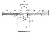
- FIG. 3illustrates a cross-sectional view of a die picking system illustrating an embodiment of the present invention. Included in FIG. 3 are a plurality of semiconductor die 301 - 305 , wherein the bottom surface of the semiconductor die are attached to an adhesive film 32 .
- the adhesive filmis mounted a rigid frame (not shown) and placed on an X-Y table (not shown) that controls relative alignment of respective die in the die picking apparatus.
- the X-Y tableis controlled by a series of stepper motors, as know to one of ordinary skill.
- the adhesive film 32overlies an anvil 33 .
- the anvil 33includes an aperture opening 331 having a location corresponding with a position for die pick-up processing for a semiconductor die, such as for example die 303 .
- a soft rubber vacuum pickup 38assists in the detachment of the die from the adhesive film 32 and transports the die 303 , after the die separation, to a package (not shown) for subsequent die attach processing.
- the plunge-up blade 34 and blade holder 36replace the prior art needle(s) shown in prior art FIGS. 1 and 2 .
- FIGS. 4 , 5 , and 6are non-limiting embodiments illustrating examples of designs for the plunge-up blade holder 36 , the plunge-up blade 34 , and the anvil 33 , respectively, for use with the present invention.
- FIG. 4Shown in FIG. 4 is a top view 361 and side view 362 of the blade holder 36 that includes the plunge-up blade 34 .
- FIG. 4Shown in the top view of FIG. 4 , one specific implementation of the blade holder design illustrates that it may be cylindrically shaped having a groove 40 that extends through its diameter.
- the groove 40is slightly wider than the width of the blade 34 .
- the blade 34is positioned in the groove 40 , set to a desired inclined position as indicated by the angle 42 , and then secured with setscrew 37 .
- the blademay be integrally formed as part of the blade holder, or a variety of other blade 34 and groove 40 configurations may be incorporated.
- a groove or a slotmay be milled in the blade holder at a predetermined angle thereby eliminating the need to manually align the blade.
- the degree of the angle and the blade lengthare dependent on a variety of factors, such as the size (length and width) and thickness of the die, characteristics of the adhesive film 32 , and operational speed of the die picking system. These factors will become apparent during subsequent discussion with respect to operation of the die picking system.
- FIG. 5Shown in FIG. 5 is a cross-sectional view 341 and a side view 342 of the blade 34 shown in FIGS. 3 and 4 .
- the blade 34is designed to have a width 52 of approximately 127 microns (5-mil). For the purposes of this specification 1-mil is equal to 0.001 inches.
- the top portion 50 of the blade 34is rounded, wherein the radius of the top rounded portion of the top surface is approximately 127 microns.
- a radius substantially less than 5-milmay cause problems with puncturing the adhesive film 32 during the die picking operation.
- diameters significantly greater than 5 milsuch as for example, approximately 508 microns (20-mil) allows too much surface area of the blade to contact adhesive film 32 , thereby impeding pick-up of the die by the soft rubber vacuum pickup due to insufficient delamination of the die from the tape.
- FIG. 5is an illustration of the side view 342 of the plunge-up blade 34 .
- Dimensions 54should be selected such that it corresponds generally to the length or width of a die such as die 303 shown in FIG. 3 .
- this length 54may depend on a variety of factors that include the dimensions and shape of the die, the adhesive strength of the adhesive film 32 , and the amount of vacuum applied by the soft rubber vacuum pickup, which will be discussed subsequently.
- a rectangle design where the bottom edge 501 is rounded similar to edge corresponding to the top portion of the blade 50may be incorporated to increase the overall life and use of the blade 34 .
- edge 501used to perform the die picking operation.
- edge 502is illustrated as being substantially flat with respect to extending along the length 54 , it also may be advantageous to slightly curve the edge 502 to create a bend in the surface extending along the length 54 to additionally promote peeling of the die from the adhesive tape.
- the previously disclosed designmay be characterized as an I-blade design wherein the blade is continuous and extends along a single axis in a single direction.
- the present inventionalso contemplates alternative designs, which may include multiple blades that may extend along more than one axis.
- an X-blade, Y-blade, V-blade or multiple finger-blade designcan be incorporated wherein multiple blades contact the adhesive tape along more than one axis to disengage the die. Multiple blade configurations may be particularly helpful by strategically distributing the force exerted on the die during the pick-up operation.
- the bladecan be designed to include slots, whereby the surface of the blade discontinuous, further reducing the surface area of the blade actually contacting the adhesive tape during the lifting operation.
- FIG. 6Shown in FIG. 6 is an anvil 33 designed for use with the plunge-up blade 34 .
- Opening 331corresponds to the opening 331 in FIG. 3 and is designed to accommodate movement of the plunge-up blade 34 through it.
- vacuum ports 333are shown on the anvil 33 .
- the vacuum portsare used to secure the adhesive film and die during the die picking operation. For example, after the tape 32 attached to dice 301 - 305 has been moved to a processing position over the opening 331 by way of an X-Y table, vacuum is applied through the vacuum ports 333 to secure the adhesive tape 32 to the anvil base.
- problemscan be encountered with the adhesive film 32 becoming punctured using prior art pins. When this happens problems may be encountered with the ability to adequately secure the adhesive film 32 to the anvil via the vacuum.
- the present inventionis therefore also advantageous from the standpoint that the potential for such punctures is substantially reduced.
- FIGS. 3 and 7 - 10are a series of processing steps illustrating the use of the plunge-up blade 34 to effectively remove a die 303 from an adhesive film 32 during the die picking portion of a die attach operation.
- die 303has been positioned to a processing position corresponding to the opening 331 of the anvil 33 .
- the primary surface 3031 of the semiconductor die 303is substantially parallel with the surface 332 of the anvil 33 , as shown in FIG. 3 .
- the plunge-up blade 34 and blade holder 36are in a retracted position relative to the base of the anvil 33 . Referring now to FIG.
- the plunge-up blade 34 and blade holder 36have been moved to a position where the plunge-up blade 34 is projected through the opening 331 thereby lifting an edge portion of die 303 such that the die is elevated above the plane of the anvil at an angle that substantially corresponds to the incline of the blade 34 .
- the angled blade 34simultaneously supports the die while promoting peeling during the lifting step, which facilitates separation of the die 303 from the adhesive film 32 with minimal damage to die.
- GaAs diewhich are much more brittle than semiconductor substrate types such as monocrystalline silicon.
- the bladeprovides support for the semiconductor die 303 while it is being lifted above the processing plane of the base of the anvil, thereby reducing stress concentration and distributing the pressure exerted by the blade across a greater surface area of the backside of semiconductor die 303 , as compared to the prior art needles.
- the bladeis oriented diagonally relative to the length (or width) of the die 303 .
- the blademay also be oriented in directions that are substantially parallel to the length (or width) of the die, or when using multiple blades, they may extend in any combination of directions. A combination of the peeling effect and added support contribute significantly to the overall reduction in fractures observed during die picking operations.
- the fracturesare most notably observed on gallium arsenide die having a thickness less than approximately 63.5 microns (2.5-mil) when using prior art needles to lift the die.
- the present inventionhas been successfully used to lift gallium arsenide die having a thickness of less than approximately 25.4 microns (1.0 mil) without producing die fractures.
- One of ordinary skill in the artrecognizes however, that the present invention is not limited to any specific semiconductor device substrate thickness or any particular substrate type.
- the soft rubber vacuum pickup 38is moved into a position that corresponds with a pick-up position to contact or nearly contact the die 303 when the plunge-up blade 34 is in its extended position.
- the positioning of the soft rubber vacuum pickup 38can occur prior to, during, or after extension of the blade.
- the vacuum 70is on or turned on.
- the die 303is now securely mounted to the soft rubber vacuum pickup 38 via the vacuum 70 .
- the soft rubber vacuum pickup 38which is holding the die can be moved to a subsequent stage of the die attach operation.
- the plunge-up blade 34 and blade holder 36have been moved to their retracted position and the soft rubber vacuum pickup holding die 303 has now been moved to a position for package mounting.
- the adhesive film 32has substantially retained its original shape and is puncture free.
- the die picking process step for die 303 with respect to the plunge-up bladeis substantially complete.
- the vacuum applied to the backside of the adhesive film 32 through the vacuum ports of anvil 33is turned off and the adhesive tape 32 and dice are moved into a position for die lifting processing of subsequent die.
- the adhesive film 32has been positioned such that die 304 is now in a processing position on the anvil 33 and ready for processing in the die picking operation.
Landscapes
- Engineering & Computer Science (AREA)
- Physics & Mathematics (AREA)
- Condensed Matter Physics & Semiconductors (AREA)
- General Physics & Mathematics (AREA)
- Manufacturing & Machinery (AREA)
- Computer Hardware Design (AREA)
- Microelectronics & Electronic Packaging (AREA)
- Power Engineering (AREA)
- Perforating, Stamping-Out Or Severing By Means Other Than Cutting (AREA)
- Container, Conveyance, Adherence, Positioning, Of Wafer (AREA)
- Encapsulation Of And Coatings For Semiconductor Or Solid State Devices (AREA)
- Adhesive Tapes (AREA)
Abstract
Description
Claims (10)
Priority Applications (4)
| Application Number | Priority Date | Filing Date | Title |
|---|---|---|---|
| US10/077,538US6889427B2 (en) | 2002-02-15 | 2002-02-15 | Process for disengaging semiconductor die from an adhesive film |
| AU2003209055AAU2003209055A1 (en) | 2002-02-15 | 2003-02-07 | Process and apparatus for disengaging semiconductor die from an adhesive film |
| PCT/US2003/003757WO2003071848A1 (en) | 2002-02-15 | 2003-02-07 | Process and apparatus for disengaging semiconductor die from an adhesive film |
| TW092103107ATWI263289B (en) | 2002-02-15 | 2003-02-14 | Process and apparatus for disengaging semiconductor die from an adhesive film |
Applications Claiming Priority (1)
| Application Number | Priority Date | Filing Date | Title |
|---|---|---|---|
| US10/077,538US6889427B2 (en) | 2002-02-15 | 2002-02-15 | Process for disengaging semiconductor die from an adhesive film |
Publications (2)
| Publication Number | Publication Date |
|---|---|
| US20030154597A1 US20030154597A1 (en) | 2003-08-21 |
| US6889427B2true US6889427B2 (en) | 2005-05-10 |
Family
ID=27732673
Family Applications (1)
| Application Number | Title | Priority Date | Filing Date |
|---|---|---|---|
| US10/077,538Expired - LifetimeUS6889427B2 (en) | 2002-02-15 | 2002-02-15 | Process for disengaging semiconductor die from an adhesive film |
Country Status (4)
| Country | Link |
|---|---|
| US (1) | US6889427B2 (en) |
| AU (1) | AU2003209055A1 (en) |
| TW (1) | TWI263289B (en) |
| WO (1) | WO2003071848A1 (en) |
Cited By (44)
| Publication number | Priority date | Publication date | Assignee | Title |
|---|---|---|---|---|
| US20050255673A1 (en)* | 2004-05-11 | 2005-11-17 | Asm Assembly Automation Ltd. | Apparatus and method for semicondutor chip detachment |
| US20060278986A1 (en)* | 2005-06-14 | 2006-12-14 | John Trezza | Chip capacitive coupling |
| US20060278996A1 (en)* | 2005-06-14 | 2006-12-14 | John Trezza | Active packaging |
| US20060281292A1 (en)* | 2005-06-14 | 2006-12-14 | John Trezza | Rigid-backed, membrane-based chip tooling |
| US20060281363A1 (en)* | 2005-06-14 | 2006-12-14 | John Trezza | Remote chip attachment |
| US20060281219A1 (en)* | 2005-06-14 | 2006-12-14 | John Trezza | Chip-based thermo-stack |
| US20060278981A1 (en)* | 2005-06-14 | 2006-12-14 | John Trezza | Electronic chip contact structure |
| US20060278995A1 (en)* | 2005-06-14 | 2006-12-14 | John Trezza | Chip spanning connection |
| US20060278992A1 (en)* | 2005-06-14 | 2006-12-14 | John Trezza | Post & penetration interconnection |
| US20070048120A1 (en)* | 2005-08-15 | 2007-03-01 | Texas Instruments Incorporated | Vacuum shroud for a die attach tool |
| US20070069340A1 (en)* | 2005-09-29 | 2007-03-29 | Semiconductor Energy Laboratory Co., Ltd. | Pickup device and pickup method |
| WO2006138493A3 (en)* | 2005-06-14 | 2007-04-19 | Cubic Wafer Inc | Chip tooling |
| US20070161235A1 (en)* | 2005-06-14 | 2007-07-12 | John Trezza | Back-to-front via process |
| US20070228539A1 (en)* | 2004-04-13 | 2007-10-04 | Unaxis International Trading Ltd., A Swiss Corporation | Method for detaching a semiconductor chip from a foil and device for mounting semiconductor chips |
| US20070246165A1 (en)* | 2003-10-02 | 2007-10-25 | Sony Corporation | Method of producing semiconductor package, apparatus for producing semiconductor package, and adhesive film |
| US20070278641A1 (en)* | 2005-06-14 | 2007-12-06 | John Trezza | Side Stacking Apparatus and Method |
| US20070281460A1 (en)* | 2006-06-06 | 2007-12-06 | Cubic Wafer, Inc. | Front-end processed wafer having through-chip connections |
| US20070281466A1 (en)* | 2006-06-06 | 2007-12-06 | John Trezza | Front-end processed wafer having through-chip connections |
| US20080086874A1 (en)* | 2006-10-16 | 2008-04-17 | Asm Assembly Automation Ltd. | Die detachment apparatus comprising pre-peeling structure |
| US20080172869A1 (en)* | 2007-01-23 | 2008-07-24 | Micron Technology, Inc. | Methods and systems for processing semiconductor workpieces |
| US20090191029A1 (en)* | 2008-01-30 | 2009-07-30 | Taeg Ki Lim | System for handling semiconductor dies |
| US20100037445A1 (en)* | 2006-06-19 | 2010-02-18 | Samsung Electronics Co., Ltd. | Method of and apparatus for detaching semiconductor chips from a tape |
| US7670874B2 (en) | 2007-02-16 | 2010-03-02 | John Trezza | Plated pillar package formation |
| US7851348B2 (en) | 2005-06-14 | 2010-12-14 | Abhay Misra | Routingless chip architecture |
| US20110114450A1 (en)* | 2009-11-18 | 2011-05-19 | Ev Group E. Thallner Gmbh | Transport system for accommodating and transporting flexible substrates |
| US20120211172A1 (en)* | 2011-02-17 | 2012-08-23 | Semikron Elektronik GmbH & Ko. KG | Apparatus and Method to Remove At Least One Chip-Like Semiconductor Component from a Film |
| US20120216396A1 (en)* | 2011-02-28 | 2012-08-30 | Pradeep Kumar Rai | Non-uniform vacuum profile die attach tip |
| US20130026212A1 (en)* | 2011-07-06 | 2013-01-31 | Flextronics Ap, Llc | Solder deposition system and method for metal bumps |
| US8456015B2 (en) | 2005-06-14 | 2013-06-04 | Cufer Asset Ltd. L.L.C. | Triaxial through-chip connection |
| US20140193232A1 (en)* | 2013-01-10 | 2014-07-10 | Epistar Corporation | Apparatus for flipping semiconductor device |
| US9111984B2 (en) | 2013-10-28 | 2015-08-18 | Freescale Semiconductor Inc. | Devices and methods of operation for separating semiconductor die from adhesive tape |
| US9196520B1 (en) | 2014-08-01 | 2015-11-24 | Freescale Semiconductor, Inc. | Tape release systems and methods for semiconductor dies |
| US20160118362A1 (en)* | 2014-10-23 | 2016-04-28 | Samsung Electronics Co., Ltd. | Bonding apparatus and substrate manufacturing equipment including the same |
| US9633883B2 (en)* | 2015-03-20 | 2017-04-25 | Rohinni, LLC | Apparatus for transfer of semiconductor devices |
| US20180122673A1 (en)* | 2016-11-03 | 2018-05-03 | Rohinni, LLC | Compliant Needle for Direct Transfer of Semiconductor Devices |
| TWI630674B (en)* | 2013-01-10 | 2018-07-21 | 晶元光電股份有限公司 | Semiconductor device transfer apparatus |
| US10062588B2 (en) | 2017-01-18 | 2018-08-28 | Rohinni, LLC | Flexible support substrate for transfer of semiconductor devices |
| US10297478B2 (en)* | 2016-11-23 | 2019-05-21 | Rohinni, LLC | Method and apparatus for embedding semiconductor devices |
| US10410905B1 (en)* | 2018-05-12 | 2019-09-10 | Rohinni, LLC | Method and apparatus for direct transfer of multiple semiconductor devices |
| US10471545B2 (en) | 2016-11-23 | 2019-11-12 | Rohinni, LLC | Top-side laser for direct transfer of semiconductor devices |
| US10504767B2 (en) | 2016-11-23 | 2019-12-10 | Rohinni, LLC | Direct transfer apparatus for a pattern array of semiconductor device die |
| US11094571B2 (en) | 2018-09-28 | 2021-08-17 | Rohinni, LLC | Apparatus to increase transferspeed of semiconductor devices with micro-adjustment |
| US11239104B2 (en) | 2019-03-12 | 2022-02-01 | Samsung Electronics Co., Ltd. | Chip ejecting apparatus |
| US20230317500A1 (en)* | 2022-03-31 | 2023-10-05 | Intel Corporation | Heat-assisted die ejection system |
Families Citing this family (10)
| Publication number | Priority date | Publication date | Assignee | Title |
|---|---|---|---|---|
| US7303647B2 (en)* | 2004-10-29 | 2007-12-04 | Asm Assembly Automation Ltd. | Driving mechanism for chip detachment apparatus |
| WO2009056469A1 (en)* | 2007-10-31 | 2009-05-07 | Oerlikon Assembly Equipment Ag, Steinhausen | Foil perforating needle for detaching a small die from a foil |
| TWI427713B (en)* | 2008-10-23 | 2014-02-21 | Gallant Prec Machining Co Ltd | Seperation method for a chip from tape film and a chip pickup method |
| MY150953A (en)* | 2008-11-05 | 2014-03-31 | Esec Ag | Die-ejector |
| CN102044404B (en)* | 2009-10-12 | 2015-12-09 | 桑迪士克科技公司 | To tape the system be separated for making semiconductor die and nude film through cutting |
| DE102012013370B4 (en)* | 2012-07-04 | 2017-11-23 | Fraunhofer-Gesellschaft zur Förderung der angewandten Forschung e.V. | Mounting device and method for fixing a needle in a needle holder of an ejection device for lifting a chip from a carrier material |
| TW201417195A (en)* | 2012-10-23 | 2014-05-01 | Wecon Automation Corp | Circular type die placing method |
| DE102013210850B3 (en)* | 2013-06-11 | 2014-03-27 | Infineon Technologies Ag | Method for manufacturing semiconductor module, involves carrying out removal of adhesive upper surface of circuit carrier, locating projections from bottom face of carrier, and inserting circuit carrier in through-holes of adhesion carrier |
| JP6627449B2 (en)* | 2015-11-20 | 2020-01-08 | 富士ゼロックス株式会社 | Gripping device, element manufacturing method, substrate device manufacturing method |
| TWI821679B (en)* | 2020-08-25 | 2023-11-11 | 南韓商杰宜斯科技有限公司 | Wafer processing apparatus and wafer processing method |
Citations (18)
| Publication number | Priority date | Publication date | Assignee | Title |
|---|---|---|---|---|
| JPS5715431A (en) | 1980-06-30 | 1982-01-26 | Mitsubishi Electric Corp | Pushing up collet of automatic die bonder |
| JPS6263441A (en) | 1985-09-13 | 1987-03-20 | Nec Corp | Semiconductor device manufacturing equipment |
| US4667402A (en)* | 1983-10-07 | 1987-05-26 | Siemens Aktiengesellschaft | Method for micro-pack production |
| JPS62128139A (en) | 1985-11-29 | 1987-06-10 | Toshiba Corp | Peeling device |
| JPS6468938A (en) | 1987-09-09 | 1989-03-15 | Kyushu Nippon Electric | Removal of defective semiconductor element |
| US4850780A (en)* | 1987-09-28 | 1989-07-25 | Kulicke And Soffa Industries Inc. | Pre-peel die ejector apparatus |
| US4859269A (en)* | 1987-08-31 | 1989-08-22 | Sumitomo Electric Industries, Ltd. | Chip mounting apparatus |
| JPH05121525A (en) | 1991-10-25 | 1993-05-18 | Sharp Corp | Picking-up method of chip |
| US5270260A (en)* | 1990-08-23 | 1993-12-14 | Siemens Aktiengesellschaft | Method and apparatus for connecting a semiconductor chip to a carrier system |
| US5343363A (en) | 1992-12-21 | 1994-08-30 | Delco Electronics Corporation | Split backed pressure sensitive die carrier tape |
| US5411921A (en)* | 1992-02-10 | 1995-05-02 | Rohm Co., Ltd. | Semiconductor chip die bonding using a double-sided adhesive tape |
| JPH07249674A (en) | 1994-03-10 | 1995-09-26 | Sony Corp | Method and device for manufacturing semiconductor device |
| US5524765A (en) | 1994-11-15 | 1996-06-11 | Tempo G | Carrier tape packaging system utilizing a layer of gel for retaining small components |
| US5589029A (en)* | 1994-07-21 | 1996-12-31 | Matsushita Electric Industrial Co., Ltd. | Semiconductor chip-supply method and apparatus |
| JPH10189690A (en) | 1996-12-26 | 1998-07-21 | Hitachi Ltd | Semiconductor chip pickup method and pickup device |
| US6201306B1 (en)* | 1995-12-05 | 2001-03-13 | Kabushiki Kaisha Toshiba | Push-up pin of a semiconductor element pushing-up device, and a method for separating |
| US6204092B1 (en)* | 1999-04-13 | 2001-03-20 | Lucent Technologies, Inc. | Apparatus and method for transferring semiconductor die to a carrier |
| US6589809B1 (en)* | 2001-07-16 | 2003-07-08 | Micron Technology, Inc. | Method for attaching semiconductor components to a substrate using local UV curing of dicing tape |
- 2002
- 2002-02-15USUS10/077,538patent/US6889427B2/ennot_activeExpired - Lifetime
- 2003
- 2003-02-07WOPCT/US2003/003757patent/WO2003071848A1/ennot_activeApplication Discontinuation
- 2003-02-07AUAU2003209055Apatent/AU2003209055A1/ennot_activeAbandoned
- 2003-02-14TWTW092103107Apatent/TWI263289B/ennot_activeIP Right Cessation
Patent Citations (19)
| Publication number | Priority date | Publication date | Assignee | Title |
|---|---|---|---|---|
| JPS5715431A (en) | 1980-06-30 | 1982-01-26 | Mitsubishi Electric Corp | Pushing up collet of automatic die bonder |
| US4667402A (en)* | 1983-10-07 | 1987-05-26 | Siemens Aktiengesellschaft | Method for micro-pack production |
| JPS6263441A (en) | 1985-09-13 | 1987-03-20 | Nec Corp | Semiconductor device manufacturing equipment |
| JPS62128139A (en) | 1985-11-29 | 1987-06-10 | Toshiba Corp | Peeling device |
| US4859269A (en)* | 1987-08-31 | 1989-08-22 | Sumitomo Electric Industries, Ltd. | Chip mounting apparatus |
| JPS6468938A (en) | 1987-09-09 | 1989-03-15 | Kyushu Nippon Electric | Removal of defective semiconductor element |
| US4850780A (en)* | 1987-09-28 | 1989-07-25 | Kulicke And Soffa Industries Inc. | Pre-peel die ejector apparatus |
| US5270260A (en)* | 1990-08-23 | 1993-12-14 | Siemens Aktiengesellschaft | Method and apparatus for connecting a semiconductor chip to a carrier system |
| JPH05121525A (en) | 1991-10-25 | 1993-05-18 | Sharp Corp | Picking-up method of chip |
| US5411921A (en)* | 1992-02-10 | 1995-05-02 | Rohm Co., Ltd. | Semiconductor chip die bonding using a double-sided adhesive tape |
| US5343363A (en) | 1992-12-21 | 1994-08-30 | Delco Electronics Corporation | Split backed pressure sensitive die carrier tape |
| JPH07249674A (en) | 1994-03-10 | 1995-09-26 | Sony Corp | Method and device for manufacturing semiconductor device |
| US5589029A (en)* | 1994-07-21 | 1996-12-31 | Matsushita Electric Industrial Co., Ltd. | Semiconductor chip-supply method and apparatus |
| US5524765A (en) | 1994-11-15 | 1996-06-11 | Tempo G | Carrier tape packaging system utilizing a layer of gel for retaining small components |
| US6201306B1 (en)* | 1995-12-05 | 2001-03-13 | Kabushiki Kaisha Toshiba | Push-up pin of a semiconductor element pushing-up device, and a method for separating |
| US6555418B2 (en)* | 1995-12-05 | 2003-04-29 | Kabushiki Kaisha Toshiba | Method for separating a semiconductor element in a semiconductor element pushing-up device |
| JPH10189690A (en) | 1996-12-26 | 1998-07-21 | Hitachi Ltd | Semiconductor chip pickup method and pickup device |
| US6204092B1 (en)* | 1999-04-13 | 2001-03-20 | Lucent Technologies, Inc. | Apparatus and method for transferring semiconductor die to a carrier |
| US6589809B1 (en)* | 2001-07-16 | 2003-07-08 | Micron Technology, Inc. | Method for attaching semiconductor components to a substrate using local UV curing of dicing tape |
Non-Patent Citations (1)
| Title |
|---|
| PCT/US03/03757 PCT Search Report mailed May 9, 2003. |
Cited By (128)
| Publication number | Priority date | Publication date | Assignee | Title |
|---|---|---|---|---|
| US20070246165A1 (en)* | 2003-10-02 | 2007-10-25 | Sony Corporation | Method of producing semiconductor package, apparatus for producing semiconductor package, and adhesive film |
| US7719125B2 (en)* | 2004-04-13 | 2010-05-18 | Unaxis International Trading Ltd. | Method for detaching a semiconductor chip from a foil and device for mounting semiconductor chips |
| US20070228539A1 (en)* | 2004-04-13 | 2007-10-04 | Unaxis International Trading Ltd., A Swiss Corporation | Method for detaching a semiconductor chip from a foil and device for mounting semiconductor chips |
| US7240422B2 (en)* | 2004-05-11 | 2007-07-10 | Asm Assembly Automation Ltd. | Apparatus for semiconductor chip detachment |
| US20050255673A1 (en)* | 2004-05-11 | 2005-11-17 | Asm Assembly Automation Ltd. | Apparatus and method for semicondutor chip detachment |
| US8154131B2 (en) | 2005-06-14 | 2012-04-10 | Cufer Asset Ltd. L.L.C. | Profiled contact |
| US20060278986A1 (en)* | 2005-06-14 | 2006-12-14 | John Trezza | Chip capacitive coupling |
| US20060281363A1 (en)* | 2005-06-14 | 2006-12-14 | John Trezza | Remote chip attachment |
| US20060281219A1 (en)* | 2005-06-14 | 2006-12-14 | John Trezza | Chip-based thermo-stack |
| US20060278331A1 (en)* | 2005-06-14 | 2006-12-14 | Roger Dugas | Membrane-based chip tooling |
| US20060278981A1 (en)* | 2005-06-14 | 2006-12-14 | John Trezza | Electronic chip contact structure |
| US20060278995A1 (en)* | 2005-06-14 | 2006-12-14 | John Trezza | Chip spanning connection |
| US20060278992A1 (en)* | 2005-06-14 | 2006-12-14 | John Trezza | Post & penetration interconnection |
| US7838997B2 (en) | 2005-06-14 | 2010-11-23 | John Trezza | Remote chip attachment |
| US8846445B2 (en) | 2005-06-14 | 2014-09-30 | Cufer Asset Ltd. L.L.C. | Inverse chip connector |
| WO2006138493A3 (en)* | 2005-06-14 | 2007-04-19 | Cubic Wafer Inc | Chip tooling |
| US20060281307A1 (en)* | 2005-06-14 | 2006-12-14 | John Trezza | Post-attachment chip-to-chip connection |
| US20070161235A1 (en)* | 2005-06-14 | 2007-07-12 | John Trezza | Back-to-front via process |
| US20070167004A1 (en)* | 2005-06-14 | 2007-07-19 | John Trezza | Triaxial through-chip connection |
| US20070182020A1 (en)* | 2005-06-14 | 2007-08-09 | John Trezza | Chip connector |
| US20070196948A1 (en)* | 2005-06-14 | 2007-08-23 | John Trezza | Stacked chip-based system and method |
| US20060278966A1 (en)* | 2005-06-14 | 2006-12-14 | John Trezza | Contact-based encapsulation |
| US20060281292A1 (en)* | 2005-06-14 | 2006-12-14 | John Trezza | Rigid-backed, membrane-based chip tooling |
| US20070278641A1 (en)* | 2005-06-14 | 2007-12-06 | John Trezza | Side Stacking Apparatus and Method |
| US20060278993A1 (en)* | 2005-06-14 | 2006-12-14 | John Trezza | Chip connector |
| US8093729B2 (en) | 2005-06-14 | 2012-01-10 | Cufer Asset Ltd. L.L.C. | Electrically conductive interconnect system and method |
| US9324629B2 (en) | 2005-06-14 | 2016-04-26 | Cufer Asset Ltd. L.L.C. | Tooling for coupling multiple electronic chips |
| US9147635B2 (en) | 2005-06-14 | 2015-09-29 | Cufer Asset Ltd. L.L.C. | Contact-based encapsulation |
| US7482272B2 (en) | 2005-06-14 | 2009-01-27 | John Trezza | Through chip connection |
| US7521806B2 (en) | 2005-06-14 | 2009-04-21 | John Trezza | Chip spanning connection |
| US7534722B2 (en) | 2005-06-14 | 2009-05-19 | John Trezza | Back-to-front via process |
| US7538033B2 (en) | 2005-06-14 | 2009-05-26 | John Trezza | Post-attachment chip-to-chip connection |
| US20090137116A1 (en)* | 2005-06-14 | 2009-05-28 | Cufer Asset Ltd. L.L.C. | Isolating chip-to-chip contact |
| US7560813B2 (en) | 2005-06-14 | 2009-07-14 | John Trezza | Chip-based thermo-stack |
| US8197627B2 (en) | 2005-06-14 | 2012-06-12 | Cufer Asset Ltd. L.L.C. | Pin-type chip tooling |
| US7659202B2 (en) | 2005-06-14 | 2010-02-09 | John Trezza | Triaxial through-chip connection |
| US8232194B2 (en) | 2005-06-14 | 2012-07-31 | Cufer Asset Ltd. L.L.C. | Process for chip capacitive coupling |
| US8643186B2 (en) | 2005-06-14 | 2014-02-04 | Cufer Asset Ltd. L.L.C. | Processed wafer via |
| US8456015B2 (en) | 2005-06-14 | 2013-06-04 | Cufer Asset Ltd. L.L.C. | Triaxial through-chip connection |
| US7687400B2 (en) | 2005-06-14 | 2010-03-30 | John Trezza | Side stacking apparatus and method |
| US8084851B2 (en) | 2005-06-14 | 2011-12-27 | Cufer Asset Ltd. L.L.C. | Side stacking apparatus and method |
| US20060278996A1 (en)* | 2005-06-14 | 2006-12-14 | John Trezza | Active packaging |
| US7767493B2 (en) | 2005-06-14 | 2010-08-03 | John Trezza | Post & penetration interconnection |
| US7781886B2 (en) | 2005-06-14 | 2010-08-24 | John Trezza | Electronic chip contact structure |
| US7785987B2 (en) | 2005-06-14 | 2010-08-31 | John Trezza | Isolating chip-to-chip contact |
| US7786592B2 (en) | 2005-06-14 | 2010-08-31 | John Trezza | Chip capacitive coupling |
| US7785931B2 (en) | 2005-06-14 | 2010-08-31 | John Trezza | Chip-based thermo-stack |
| US7808111B2 (en) | 2005-06-14 | 2010-10-05 | John Trezza | Processed wafer via |
| US8197626B2 (en) | 2005-06-14 | 2012-06-12 | Cufer Asset Ltd. L.L.C. | Rigid-backed, membrane-based chip tooling |
| US7847412B2 (en) | 2005-06-14 | 2010-12-07 | John Trezza | Isolating chip-to-chip contact |
| US7851348B2 (en) | 2005-06-14 | 2010-12-14 | Abhay Misra | Routingless chip architecture |
| US7884483B2 (en) | 2005-06-14 | 2011-02-08 | Cufer Asset Ltd. L.L.C. | Chip connector |
| US7919870B2 (en) | 2005-06-14 | 2011-04-05 | Cufer Asset Ltd. L.L.C. | Coaxial through chip connection |
| US7932584B2 (en) | 2005-06-14 | 2011-04-26 | Cufer Asset Ltd. L.L.C. | Stacked chip-based system and method |
| US7942182B2 (en) | 2005-06-14 | 2011-05-17 | Cufer Asset Ltd. L.L.C. | Rigid-backed, membrane-based chip tooling |
| US8283778B2 (en) | 2005-06-14 | 2012-10-09 | Cufer Asset Ltd. L.L.C. | Thermally balanced via |
| US7946331B2 (en) | 2005-06-14 | 2011-05-24 | Cufer Asset Ltd. L.L.C. | Pin-type chip tooling |
| US7969015B2 (en) | 2005-06-14 | 2011-06-28 | Cufer Asset Ltd. L.L.C. | Inverse chip connector |
| US7989958B2 (en) | 2005-06-14 | 2011-08-02 | Cufer Assett Ltd. L.L.C. | Patterned contact |
| US8021922B2 (en) | 2005-06-14 | 2011-09-20 | Cufer Asset Ltd. L.L.C. | Remote chip attachment |
| US8053903B2 (en) | 2005-06-14 | 2011-11-08 | Cufer Asset Ltd. L.L.C. | Chip capacitive coupling |
| US8067312B2 (en) | 2005-06-14 | 2011-11-29 | Cufer Asset Ltd. L.L.C. | Coaxial through chip connection |
| US20070048120A1 (en)* | 2005-08-15 | 2007-03-01 | Texas Instruments Incorporated | Vacuum shroud for a die attach tool |
| US8137050B2 (en)* | 2005-09-29 | 2012-03-20 | Semiconductor Energy Laboratory Co., Ltd. | Pickup device and pickup method |
| US20070069340A1 (en)* | 2005-09-29 | 2007-03-29 | Semiconductor Energy Laboratory Co., Ltd. | Pickup device and pickup method |
| US7687397B2 (en) | 2006-06-06 | 2010-03-30 | John Trezza | Front-end processed wafer having through-chip connections |
| US20070281466A1 (en)* | 2006-06-06 | 2007-12-06 | John Trezza | Front-end processed wafer having through-chip connections |
| US20070281460A1 (en)* | 2006-06-06 | 2007-12-06 | Cubic Wafer, Inc. | Front-end processed wafer having through-chip connections |
| US20100037445A1 (en)* | 2006-06-19 | 2010-02-18 | Samsung Electronics Co., Ltd. | Method of and apparatus for detaching semiconductor chips from a tape |
| US20080086874A1 (en)* | 2006-10-16 | 2008-04-17 | Asm Assembly Automation Ltd. | Die detachment apparatus comprising pre-peeling structure |
| US7665204B2 (en)* | 2006-10-16 | 2010-02-23 | Asm Assembly Automation Ltd. | Die detachment apparatus comprising pre-peeling structure |
| US20080172869A1 (en)* | 2007-01-23 | 2008-07-24 | Micron Technology, Inc. | Methods and systems for processing semiconductor workpieces |
| US7670874B2 (en) | 2007-02-16 | 2010-03-02 | John Trezza | Plated pillar package formation |
| US20090191029A1 (en)* | 2008-01-30 | 2009-07-30 | Taeg Ki Lim | System for handling semiconductor dies |
| US20110114450A1 (en)* | 2009-11-18 | 2011-05-19 | Ev Group E. Thallner Gmbh | Transport system for accommodating and transporting flexible substrates |
| US8931624B2 (en)* | 2009-11-18 | 2015-01-13 | Ev Group E. Thallner Gmbh | Transport system for accommodating and transporting flexible substrates |
| US8470131B2 (en)* | 2011-02-17 | 2013-06-25 | Semikron Elektronik Gmbh & Co., Kg | Apparatus and method to remove at least one chip-like semiconductor component from a film |
| US20120211172A1 (en)* | 2011-02-17 | 2012-08-23 | Semikron Elektronik GmbH & Ko. KG | Apparatus and Method to Remove At Least One Chip-Like Semiconductor Component from a Film |
| US9038264B2 (en)* | 2011-02-28 | 2015-05-26 | Sandisk Semiconductor (Shanghai) Co., Ltd. | Non-uniform vacuum profile die attach tip |
| US20120216396A1 (en)* | 2011-02-28 | 2012-08-30 | Pradeep Kumar Rai | Non-uniform vacuum profile die attach tip |
| US20130026212A1 (en)* | 2011-07-06 | 2013-01-31 | Flextronics Ap, Llc | Solder deposition system and method for metal bumps |
| TWI571949B (en)* | 2013-01-10 | 2017-02-21 | 晶元光電股份有限公司 | Semiconductor device transfer apparatus |
| TWI630674B (en)* | 2013-01-10 | 2018-07-21 | 晶元光電股份有限公司 | Semiconductor device transfer apparatus |
| US20140193232A1 (en)* | 2013-01-10 | 2014-07-10 | Epistar Corporation | Apparatus for flipping semiconductor device |
| US9754808B2 (en) | 2013-01-10 | 2017-09-05 | Epistar Corporation | Apparatus for flipping semiconductor device for transferring the semiconductor device between substrates |
| US9209058B2 (en)* | 2013-01-10 | 2015-12-08 | Epistar Corporation | Apparatus for flipping semiconductor device |
| US9111984B2 (en) | 2013-10-28 | 2015-08-18 | Freescale Semiconductor Inc. | Devices and methods of operation for separating semiconductor die from adhesive tape |
| US9196520B1 (en) | 2014-08-01 | 2015-11-24 | Freescale Semiconductor, Inc. | Tape release systems and methods for semiconductor dies |
| US9553069B2 (en)* | 2014-10-23 | 2017-01-24 | Samsung Electronics Co., Ltd. | Bonding apparatus and substrate manufacturing equipment including the same |
| US20160118362A1 (en)* | 2014-10-23 | 2016-04-28 | Samsung Electronics Co., Ltd. | Bonding apparatus and substrate manufacturing equipment including the same |
| US10170454B2 (en) | 2015-03-20 | 2019-01-01 | Rohinni, LLC | Method and apparatus for direct transfer of semiconductor device die from a mapped wafer |
| US11152339B2 (en) | 2015-03-20 | 2021-10-19 | Rohinni, LLC | Method for improved transfer of semiconductor die |
| US9985003B2 (en) | 2015-03-20 | 2018-05-29 | Rohinni, LLC | Substrate with array of LEDs for backlighting a display device |
| US9871023B2 (en)* | 2015-03-20 | 2018-01-16 | Rohinni, LLC | Method for transfer of semiconductor devices |
| US11562990B2 (en) | 2015-03-20 | 2023-01-24 | Rohinni, Inc. | Systems for direct transfer of semiconductor device die |
| US20180261579A1 (en)* | 2015-03-20 | 2018-09-13 | Rohinni, LLC | Method and apparatus for improved direct transfer of semiconductor die |
| US11515293B2 (en) | 2015-03-20 | 2022-11-29 | Rohinni, LLC | Direct transfer of semiconductor devices from a substrate |
| US10157896B2 (en) | 2015-03-20 | 2018-12-18 | Rohinni, LLC | Method and apparatus for light diffusion |
| US9633883B2 (en)* | 2015-03-20 | 2017-04-25 | Rohinni, LLC | Apparatus for transfer of semiconductor devices |
| US10242971B2 (en) | 2015-03-20 | 2019-03-26 | Rohinni, LLC | Apparatus for direct transfer of semiconductor devices with needle retraction support |
| US10290615B2 (en)* | 2015-03-20 | 2019-05-14 | Rohinni, LLC | Method and apparatus for improved direct transfer of semiconductor die |
| US11488940B2 (en) | 2015-03-20 | 2022-11-01 | Rohinni, Inc. | Method for transfer of semiconductor devices onto glass substrates |
| US10325885B2 (en) | 2015-03-20 | 2019-06-18 | Rohinni, LLC | Semiconductor device on string circuit and method of making the same |
| US10910354B2 (en) | 2015-03-20 | 2021-02-02 | Rohinni, LLC | Apparatus for direct transfer of semiconductor device die |
| US10361176B2 (en) | 2015-03-20 | 2019-07-23 | Rohinni, LLC | Substrate with array of LEDs for backlighting a display device |
| US10373937B2 (en) | 2015-03-20 | 2019-08-06 | Rohinni, LLC | Apparatus for multi-direct transfer of semiconductors |
| US10636770B2 (en) | 2015-03-20 | 2020-04-28 | Rohinni, LLC | Apparatus and method for direct transfer of semiconductor devices from a substrate and stacking semiconductor devices on each other |
| US10622337B2 (en) | 2015-03-20 | 2020-04-14 | Rohinni, LLC | Method and apparatus for transfer of semiconductor devices |
| US10490532B2 (en) | 2015-03-20 | 2019-11-26 | Rohinni, LLC | Apparatus and method for direct transfer of semiconductor devices |
| US10615153B2 (en) | 2015-03-20 | 2020-04-07 | Rohinni, LLC | Apparatus for direct transfer of semiconductor device die |
| US10566319B2 (en) | 2015-03-20 | 2020-02-18 | Rohinni, LLC | Apparatus for direct transfer of semiconductor device die |
| US10615152B2 (en) | 2015-03-20 | 2020-04-07 | Rohinni, LLC | Semiconductor device on glass substrate |
| US11069551B2 (en) | 2016-11-03 | 2021-07-20 | Rohinni, LLC | Method of dampening a force applied to an electrically-actuatable element |
| US10141215B2 (en)* | 2016-11-03 | 2018-11-27 | Rohinni, LLC | Compliant needle for direct transfer of semiconductor devices |
| US20180122673A1 (en)* | 2016-11-03 | 2018-05-03 | Rohinni, LLC | Compliant Needle for Direct Transfer of Semiconductor Devices |
| US11462433B2 (en) | 2016-11-23 | 2022-10-04 | Rohinni, LLC | Direct transfer apparatus for a pattern array of semiconductor device die |
| US10504767B2 (en) | 2016-11-23 | 2019-12-10 | Rohinni, LLC | Direct transfer apparatus for a pattern array of semiconductor device die |
| US10297478B2 (en)* | 2016-11-23 | 2019-05-21 | Rohinni, LLC | Method and apparatus for embedding semiconductor devices |
| US10471545B2 (en) | 2016-11-23 | 2019-11-12 | Rohinni, LLC | Top-side laser for direct transfer of semiconductor devices |
| US11538699B2 (en) | 2016-11-23 | 2022-12-27 | Rohinni, LLC | Method and apparatus for embedding semiconductor devices |
| US10354895B2 (en) | 2017-01-18 | 2019-07-16 | Rohinni, LLC | Support substrate for transfer of semiconductor devices |
| US10062588B2 (en) | 2017-01-18 | 2018-08-28 | Rohinni, LLC | Flexible support substrate for transfer of semiconductor devices |
| US10410905B1 (en)* | 2018-05-12 | 2019-09-10 | Rohinni, LLC | Method and apparatus for direct transfer of multiple semiconductor devices |
| US11094571B2 (en) | 2018-09-28 | 2021-08-17 | Rohinni, LLC | Apparatus to increase transferspeed of semiconductor devices with micro-adjustment |
| US11728195B2 (en) | 2018-09-28 | 2023-08-15 | Rohinni, Inc. | Apparatuses for executing a direct transfer of a semiconductor device die disposed on a first substrate to a second substrate |
| US12165895B2 (en) | 2018-09-28 | 2024-12-10 | Cowles Semi, Llc | Apparatuses for executing a direct transfer of a semiconductor device die disposed on a first substrate to a second substrate |
| US11239104B2 (en) | 2019-03-12 | 2022-02-01 | Samsung Electronics Co., Ltd. | Chip ejecting apparatus |
| US20230317500A1 (en)* | 2022-03-31 | 2023-10-05 | Intel Corporation | Heat-assisted die ejection system |
Also Published As
| Publication number | Publication date |
|---|---|
| WO2003071848A1 (en) | 2003-08-28 |
| US20030154597A1 (en) | 2003-08-21 |
| AU2003209055A1 (en) | 2003-09-09 |
| TW200305960A (en) | 2003-11-01 |
| TWI263289B (en) | 2006-10-01 |
Similar Documents
| Publication | Publication Date | Title |
|---|---|---|
| US6889427B2 (en) | Process for disengaging semiconductor die from an adhesive film | |
| KR100639587B1 (en) | Protective tape joining method and apparatus using the same as well as protective tape separating method and apparatus using the same | |
| US6204092B1 (en) | Apparatus and method for transferring semiconductor die to a carrier | |
| JP4754278B2 (en) | Chip body manufacturing method | |
| US6767803B2 (en) | Method for peeling protective sheet | |
| TWI292596B (en) | Manufacturing method of semiconductor device | |
| CN100392798C (en) | Thin die separation apparatus and method | |
| JP2010010207A (en) | Separating apparatus and separating method | |
| JP2003209082A (en) | Method and device for attaching protective tape and method for removing protective tape | |
| JP2002050670A (en) | Pickup device and pickup method | |
| CN108713247B (en) | Substrate transfer method and substrate transfer apparatus | |
| US20120247657A1 (en) | Substrate transfer method and substrate transfer apparatus | |
| JPH09167779A (en) | Semiconductor manufacturing equipment | |
| JP2006191144A (en) | Pickup device and pickup method | |
| US20130039733A1 (en) | Pick and place tape release for thin semiconductor dies | |
| CN101826480B (en) | Flanged Collet Body for Die Picking Tool | |
| JP2001093864A (en) | Semiconductor wafer fixing jig and method of manufacturing semiconductor device | |
| US5240882A (en) | Process and apparatus for making discrete type substrates by re-slicing a wafer | |
| JPH10189690A (en) | Semiconductor chip pickup method and pickup device | |
| JP2005109155A (en) | Semiconductor wafer processing method | |
| US6602736B1 (en) | Method and apparatus for separating semiconductor chips | |
| JP2002353296A (en) | Equipment for peeling wafer protective tape and wafer mounting equipment | |
| JP2002151528A (en) | Die bonding sheet sticking device and method of sticking die bonding sheet | |
| JP2004031535A (en) | Adhesive sheet peeling method, adhesive sheet peeling device | |
| EP0348783B1 (en) | Process of making discrete type substrates |
Legal Events
| Date | Code | Title | Description |
|---|---|---|---|
| AS | Assignment | Owner name:MOTOROLA, INC., ILLINOIS Free format text:ASSIGNMENT OF ASSIGNORS INTEREST;ASSIGNORS:YEE, LUP KWEUN;BELMAS, DARRELL JACOB;REEL/FRAME:012618/0493;SIGNING DATES FROM 20020208 TO 20020212 | |
| AS | Assignment | Owner name:FREESCALE SEMICONDUCTOR, INC., TEXAS Free format text:ASSIGNMENT OF ASSIGNORS INTEREST;ASSIGNOR:MOTOROLA, INC;REEL/FRAME:015360/0718 Effective date:20040404 Owner name:FREESCALE SEMICONDUCTOR, INC.,TEXAS Free format text:ASSIGNMENT OF ASSIGNORS INTEREST;ASSIGNOR:MOTOROLA, INC;REEL/FRAME:015360/0718 Effective date:20040404 | |
| STCF | Information on status: patent grant | Free format text:PATENTED CASE | |
| AS | Assignment | Owner name:CITIBANK, N.A. AS COLLATERAL AGENT, NEW YORK Free format text:SECURITY AGREEMENT;ASSIGNORS:FREESCALE SEMICONDUCTOR, INC.;FREESCALE ACQUISITION CORPORATION;FREESCALE ACQUISITION HOLDINGS CORP.;AND OTHERS;REEL/FRAME:018855/0129 Effective date:20061201 Owner name:CITIBANK, N.A. AS COLLATERAL AGENT,NEW YORK Free format text:SECURITY AGREEMENT;ASSIGNORS:FREESCALE SEMICONDUCTOR, INC.;FREESCALE ACQUISITION CORPORATION;FREESCALE ACQUISITION HOLDINGS CORP.;AND OTHERS;REEL/FRAME:018855/0129 Effective date:20061201 | |
| FPAY | Fee payment | Year of fee payment:4 | |
| AS | Assignment | Owner name:CITIBANK, N.A., AS COLLATERAL AGENT,NEW YORK Free format text:SECURITY AGREEMENT;ASSIGNOR:FREESCALE SEMICONDUCTOR, INC.;REEL/FRAME:024397/0001 Effective date:20100413 Owner name:CITIBANK, N.A., AS COLLATERAL AGENT, NEW YORK Free format text:SECURITY AGREEMENT;ASSIGNOR:FREESCALE SEMICONDUCTOR, INC.;REEL/FRAME:024397/0001 Effective date:20100413 | |
| FPAY | Fee payment | Year of fee payment:8 | |
| AS | Assignment | Owner name:CITIBANK, N.A., AS NOTES COLLATERAL AGENT, NEW YORK Free format text:SECURITY AGREEMENT;ASSIGNOR:FREESCALE SEMICONDUCTOR, INC.;REEL/FRAME:030633/0424 Effective date:20130521 Owner name:CITIBANK, N.A., AS NOTES COLLATERAL AGENT, NEW YOR Free format text:SECURITY AGREEMENT;ASSIGNOR:FREESCALE SEMICONDUCTOR, INC.;REEL/FRAME:030633/0424 Effective date:20130521 | |
| AS | Assignment | Owner name:CITIBANK, N.A., AS NOTES COLLATERAL AGENT, NEW YORK Free format text:SECURITY AGREEMENT;ASSIGNOR:FREESCALE SEMICONDUCTOR, INC.;REEL/FRAME:031591/0266 Effective date:20131101 Owner name:CITIBANK, N.A., AS NOTES COLLATERAL AGENT, NEW YOR Free format text:SECURITY AGREEMENT;ASSIGNOR:FREESCALE SEMICONDUCTOR, INC.;REEL/FRAME:031591/0266 Effective date:20131101 | |
| AS | Assignment | Owner name:FREESCALE SEMICONDUCTOR, INC., TEXAS Free format text:PATENT RELEASE;ASSIGNOR:CITIBANK, N.A., AS COLLATERAL AGENT;REEL/FRAME:037354/0225 Effective date:20151207 Owner name:FREESCALE SEMICONDUCTOR, INC., TEXAS Free format text:PATENT RELEASE;ASSIGNOR:CITIBANK, N.A., AS COLLATERAL AGENT;REEL/FRAME:037356/0553 Effective date:20151207 Owner name:FREESCALE SEMICONDUCTOR, INC., TEXAS Free format text:PATENT RELEASE;ASSIGNOR:CITIBANK, N.A., AS COLLATERAL AGENT;REEL/FRAME:037356/0143 Effective date:20151207 | |
| AS | Assignment | Owner name:MORGAN STANLEY SENIOR FUNDING, INC., MARYLAND Free format text:ASSIGNMENT AND ASSUMPTION OF SECURITY INTEREST IN PATENTS;ASSIGNOR:CITIBANK, N.A.;REEL/FRAME:037486/0517 Effective date:20151207 | |
| AS | Assignment | Owner name:MORGAN STANLEY SENIOR FUNDING, INC., MARYLAND Free format text:ASSIGNMENT AND ASSUMPTION OF SECURITY INTEREST IN PATENTS;ASSIGNOR:CITIBANK, N.A.;REEL/FRAME:037518/0292 Effective date:20151207 | |
| AS | Assignment | Owner name:MORGAN STANLEY SENIOR FUNDING, INC., MARYLAND Free format text:SUPPLEMENT TO THE SECURITY AGREEMENT;ASSIGNOR:FREESCALE SEMICONDUCTOR, INC.;REEL/FRAME:039138/0001 Effective date:20160525 | |
| FPAY | Fee payment | Year of fee payment:12 | |
| AS | Assignment | Owner name:NXP, B.V., F/K/A FREESCALE SEMICONDUCTOR, INC., NETHERLANDS Free format text:RELEASE BY SECURED PARTY;ASSIGNOR:MORGAN STANLEY SENIOR FUNDING, INC.;REEL/FRAME:040925/0001 Effective date:20160912 Owner name:NXP, B.V., F/K/A FREESCALE SEMICONDUCTOR, INC., NE Free format text:RELEASE BY SECURED PARTY;ASSIGNOR:MORGAN STANLEY SENIOR FUNDING, INC.;REEL/FRAME:040925/0001 Effective date:20160912 | |
| AS | Assignment | Owner name:NXP B.V., NETHERLANDS Free format text:RELEASE BY SECURED PARTY;ASSIGNOR:MORGAN STANLEY SENIOR FUNDING, INC.;REEL/FRAME:040928/0001 Effective date:20160622 | |
| AS | Assignment | Owner name:NXP USA, INC., TEXAS Free format text:CHANGE OF NAME;ASSIGNOR:FREESCALE SEMICONDUCTOR INC.;REEL/FRAME:040652/0180 Effective date:20161107 | |
| AS | Assignment | Owner name:NXP USA, INC., TEXAS Free format text:CORRECTIVE ASSIGNMENT TO CORRECT THE NATURE OF CONVEYANCE LISTED CHANGE OF NAME SHOULD BE MERGER AND CHANGE PREVIOUSLY RECORDED AT REEL: 040652 FRAME: 0180. ASSIGNOR(S) HEREBY CONFIRMS THE MERGER AND CHANGE OF NAME;ASSIGNOR:FREESCALE SEMICONDUCTOR INC.;REEL/FRAME:041354/0148 Effective date:20161107 | |
| AS | Assignment | Owner name:MORGAN STANLEY SENIOR FUNDING, INC., MARYLAND Free format text:CORRECTIVE ASSIGNMENT TO CORRECT THE REMOVE PATENTS 8108266 AND 8062324 AND REPLACE THEM WITH 6108266 AND 8060324 PREVIOUSLY RECORDED ON REEL 037518 FRAME 0292. ASSIGNOR(S) HEREBY CONFIRMS THE ASSIGNMENT AND ASSUMPTION OF SECURITY INTEREST IN PATENTS;ASSIGNOR:CITIBANK, N.A.;REEL/FRAME:041703/0536 Effective date:20151207 | |
| AS | Assignment | Owner name:SHENZHEN XINGUODU TECHNOLOGY CO., LTD., CHINA Free format text:CORRECTIVE ASSIGNMENT TO CORRECT THE TO CORRECT THE APPLICATION NO. FROM 13,883,290 TO 13,833,290 PREVIOUSLY RECORDED ON REEL 041703 FRAME 0536. ASSIGNOR(S) HEREBY CONFIRMS THE THE ASSIGNMENT AND ASSUMPTION OF SECURITYINTEREST IN PATENTS.;ASSIGNOR:MORGAN STANLEY SENIOR FUNDING, INC.;REEL/FRAME:048734/0001 Effective date:20190217 | |
| AS | Assignment | Owner name:NXP B.V., NETHERLANDS Free format text:RELEASE BY SECURED PARTY;ASSIGNOR:MORGAN STANLEY SENIOR FUNDING, INC.;REEL/FRAME:050744/0097 Effective date:20190903 | |
| AS | Assignment | Owner name:MORGAN STANLEY SENIOR FUNDING, INC., MARYLAND Free format text:CORRECTIVE ASSIGNMENT TO CORRECT THE REMOVE APPLICATION11759915 AND REPLACE IT WITH APPLICATION 11759935 PREVIOUSLY RECORDED ON REEL 037486 FRAME 0517. ASSIGNOR(S) HEREBY CONFIRMS THE ASSIGNMENT AND ASSUMPTION OF SECURITYINTEREST IN PATENTS;ASSIGNOR:CITIBANK, N.A.;REEL/FRAME:053547/0421 Effective date:20151207 | |
| AS | Assignment | Owner name:NXP B.V., NETHERLANDS Free format text:CORRECTIVE ASSIGNMENT TO CORRECT THE REMOVEAPPLICATION 11759915 AND REPLACE IT WITH APPLICATION11759935 PREVIOUSLY RECORDED ON REEL 040928 FRAME 0001. ASSIGNOR(S) HEREBY CONFIRMS THE RELEASE OF SECURITYINTEREST;ASSIGNOR:MORGAN STANLEY SENIOR FUNDING, INC.;REEL/FRAME:052915/0001 Effective date:20160622 | |
| AS | Assignment | Owner name:NXP, B.V. F/K/A FREESCALE SEMICONDUCTOR, INC., NETHERLANDS Free format text:CORRECTIVE ASSIGNMENT TO CORRECT THE REMOVEAPPLICATION 11759915 AND REPLACE IT WITH APPLICATION11759935 PREVIOUSLY RECORDED ON REEL 040925 FRAME 0001. ASSIGNOR(S) HEREBY CONFIRMS THE RELEASE OF SECURITYINTEREST;ASSIGNOR:MORGAN STANLEY SENIOR FUNDING, INC.;REEL/FRAME:052917/0001 Effective date:20160912 |