US6888997B2 - Waveguide device and optical transfer system for directing light to an image plane - Google Patents
Waveguide device and optical transfer system for directing light to an image planeDownload PDFInfo
- Publication number
- US6888997B2 US6888997B2US10/660,214US66021403AUS6888997B2US 6888997 B2US6888997 B2US 6888997B2US 66021403 AUS66021403 AUS 66021403AUS 6888997 B2US6888997 B2US 6888997B2
- Authority
- US
- United States
- Prior art keywords
- waveguide device
- light
- transmitting body
- light transmitting
- image plane
- Prior art date
- Legal status (The legal status is an assumption and is not a legal conclusion. Google has not performed a legal analysis and makes no representation as to the accuracy of the status listed.)
- Expired - Fee Related
Links
Images


Classifications
- G—PHYSICS
- G02—OPTICS
- G02B—OPTICAL ELEMENTS, SYSTEMS OR APPARATUS
- G02B6/00—Light guides; Structural details of arrangements comprising light guides and other optical elements, e.g. couplings
- G02B6/0001—Light guides; Structural details of arrangements comprising light guides and other optical elements, e.g. couplings specially adapted for lighting devices or systems
- G02B6/0011—Light guides; Structural details of arrangements comprising light guides and other optical elements, e.g. couplings specially adapted for lighting devices or systems the light guides being planar or of plate-like form
- G02B6/0033—Means for improving the coupling-out of light from the light guide
- G02B6/0035—Means for improving the coupling-out of light from the light guide provided on the surface of the light guide or in the bulk of it
- G02B6/0045—Means for improving the coupling-out of light from the light guide provided on the surface of the light guide or in the bulk of it by shaping at least a portion of the light guide
- G02B6/0046—Tapered light guide, e.g. wedge-shaped light guide
- G—PHYSICS
- G02—OPTICS
- G02B—OPTICAL ELEMENTS, SYSTEMS OR APPARATUS
- G02B6/00—Light guides; Structural details of arrangements comprising light guides and other optical elements, e.g. couplings
- G02B6/10—Light guides; Structural details of arrangements comprising light guides and other optical elements, e.g. couplings of the optical waveguide type
- G—PHYSICS
- G02—OPTICS
- G02B—OPTICAL ELEMENTS, SYSTEMS OR APPARATUS
- G02B6/00—Light guides; Structural details of arrangements comprising light guides and other optical elements, e.g. couplings
- G02B6/24—Coupling light guides
- G02B6/42—Coupling light guides with opto-electronic elements
- G02B6/4298—Coupling light guides with opto-electronic elements coupling with non-coherent light sources and/or radiation detectors, e.g. lamps, incandescent bulbs, scintillation chambers
- H—ELECTRICITY
- H04—ELECTRIC COMMUNICATION TECHNIQUE
- H04N—PICTORIAL COMMUNICATION, e.g. TELEVISION
- H04N1/00—Scanning, transmission or reproduction of documents or the like, e.g. facsimile transmission; Details thereof
- H04N1/024—Details of scanning heads ; Means for illuminating the original
- H04N1/028—Details of scanning heads ; Means for illuminating the original for picture information pick-up
- H04N1/02815—Means for illuminating the original, not specific to a particular type of pick-up head
- H04N1/0282—Using a single or a few point light sources, e.g. a laser diode
- H04N1/0284—Using a single or a few point light sources, e.g. a laser diode in combination with a light integrating, concentrating or diffusing cavity
- G—PHYSICS
- G02—OPTICS
- G02B—OPTICAL ELEMENTS, SYSTEMS OR APPARATUS
- G02B6/00—Light guides; Structural details of arrangements comprising light guides and other optical elements, e.g. couplings
- G02B2006/0098—Light guides; Structural details of arrangements comprising light guides and other optical elements, e.g. couplings for scanning
- G—PHYSICS
- G02—OPTICS
- G02B—OPTICAL ELEMENTS, SYSTEMS OR APPARATUS
- G02B6/00—Light guides; Structural details of arrangements comprising light guides and other optical elements, e.g. couplings
- G02B6/0001—Light guides; Structural details of arrangements comprising light guides and other optical elements, e.g. couplings specially adapted for lighting devices or systems
- G02B6/0011—Light guides; Structural details of arrangements comprising light guides and other optical elements, e.g. couplings specially adapted for lighting devices or systems the light guides being planar or of plate-like form
- G02B6/0033—Means for improving the coupling-out of light from the light guide
- G02B6/005—Means for improving the coupling-out of light from the light guide provided by one optical element, or plurality thereof, placed on the light output side of the light guide
- G02B6/0055—Reflecting element, sheet or layer
- G—PHYSICS
- G02—OPTICS
- G02B—OPTICAL ELEMENTS, SYSTEMS OR APPARATUS
- G02B6/00—Light guides; Structural details of arrangements comprising light guides and other optical elements, e.g. couplings
- G02B6/02—Optical fibres with cladding with or without a coating
- G02B6/032—Optical fibres with cladding with or without a coating with non solid core or cladding
- H—ELECTRICITY
- H04—ELECTRIC COMMUNICATION TECHNIQUE
- H04N—PICTORIAL COMMUNICATION, e.g. TELEVISION
- H04N2201/00—Indexing scheme relating to scanning, transmission or reproduction of documents or the like, and to details thereof
- H04N2201/04—Scanning arrangements
- H04N2201/0402—Arrangements not specific to a particular one of the scanning methods covered by groups H04N1/04 - H04N1/207
- H04N2201/0404—Scanning transparent media, e.g. photographic film
- H04N2201/0408—Scanning film strips or rolls
Definitions
- the present inventionrelates generally to light transfer devices and systems, and more particularly to a device used with a light transfer system for efficiently transferring light from a light source to an image plane.
- the collection angle in condenser systemsis generally low compared to other systems.
- the condenser systemsgenerally have a plurality of optical elements, and as such, increases the complexity of mechanically mounting each component of the system, and can increase the overall cost of the system.
- the light beamcan be easily obstructed or scattered by various objects.
- a guided-wave optical devicetransmits light through dielectric conduits, which can provide long distance light transmission without the need or use of relay lenses.
- a guided-wave optical deviceis a light conduit that is configured as either a slab, strip, or cylinder of dielectric material, and generally having a rectangular vertical cross sectional shape along its respective longitudinal axis.
- These guided-wave optic devicesutilize internal reflections to integrate and transport light to an image plane. Light reflects off the interface between the dielectric material and outside material (e.g., a material with an index of refraction less than the dielectric material, such as glass with an additive, or air) interface.
- optical devices and systemshave a number of shortcomings that can greatly reduce the amount of light and/or focus of the light being transmitted from the light source to the image plane.
- light being emitted from conventional devices and systemsis not always uniform and any source imperfections are transmitted through the device and system.
- the present inventioncomprises a waveguide device for transmitting light.
- the present inventioncomprises a waveguide device having a light transmitting body.
- the bodyincludes a first surface and a second surface, and a longitudinal axis. At least one of the first and second surfaces, and preferably both surfaces, are configured to be non-parallel to the longitudinal axis. Furthermore, the first surface is configured to be non-parallel to the second surface.
- the body of the waveguide deviceis configured in a generally elliptical shape along the longitudinal axis, whereby a proximal portion of the waveguide device is generally symmetrical with a distal portion.
- the body of the waveguide devicepreferably comprises a dielectric material, such as either a plastic material (e.g., acrylic), or a glass material.
- a dielectric materialsuch as either a plastic material (e.g., acrylic), or a glass material.
- the body of the waveguide deviceis a solid piece of material.
- the bodymay include a hollow chamber therein.
- the first and/or second surfaces of the bodymay also include a reflective coating material.
- the coatingmay be bare gold, gold, aluminum, silver, mixtures thereof, or any other suitable reflective material.
- the body of the waveguide of the present inventionmay also include an end surface that is configured to be parallel to the transverse axis of the waveguide device.
- the present inventioncomprises may include an optical transfer system having a light source operable to produce electromagnetic energy, and an elliptically configured waveguide device operable to receive electromagnetic energy from the light source.
- the waveguide devicecan direct the electromagnetic energy to an image plane.
- the waveguide deviceincludes a body having a first surface and a second surface and a longitudinal axis, at least one of the first and second surfaces is configured to be non-parallel to the longitudinal axis.
- the waveguide devicemay also include an end portion provided adjacent the image plane, and/or an end that is positioned abutting the light source.
- the present inventionmay include a digital film processing system.
- the digital film processing systemhas at least one light source operable to produce light, and an elliptically configured waveguide device operable to direct light from at least one light source, such as a source of electromagnetic radiation, to a photographic media.
- the digital film processing systemalso includes at last one optical sensor operable to detect light from the photographic media and a computer processor connected to the at least one sensor and operable to produce a digital image.
- the at least one optical sensoroperates to detect reflected and/or transmissive light from the photographic media.
- FIG. 1is a prospective view of an optical device in accordance with the present invention
- FIG. 2is a vertical sectional view of an optical device and system in accordance with the present invention.
- FIG. 3Ais a vertical sectional view of alternative embodiment of an optical device and system in accordance with the present invention.
- FIG. 3Bis a vertical sectional view of yet alternative embodiment of an optical device and system in accordance with the present invention.
- FIG. 4is a vertical sectional view of yet another embodiment of an optical device and system in accordance with the present invention.
- FIG. 5is a vertical sectional view of still another embodiment of an optical device and system in accordance with the present invention.
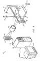
- FIG. 6is a perspective view of a digital film processing system in accordance with the present invention.
- FIGS. 1 and 2illustrate an optical transfer system 8 in accordance with one embodiment of the invention.
- the optical transfer system 8comprises a light source 12 and a waveguide device 10 .
- the light source 12 and waveguide device 10 of the optical transfer system 8can be assembled using fixtures and techniques known in the industry.
- the present inventioncan be used in a variety of suitable articles and devices desiring the collection and transfer of light, such as a digital film processing system (see FIG. 6 ), a copier, a scanner, and various medical devices.
- Light source 12 in the optical transfer system 8is generally positioned relative to the waveguide device 10 so that the transfer or transmission of light to the waveguide device 10 is optimized.
- the light source 12is positioned adjacent one end 22 of the waveguide device 10 , and preferably, in an abutting relationship with end 22 , as exemplified in FIG. 2 .
- Examples of light source 12 used with the present inventioncan include a source of electromagnetic radiation, a laser, an LED light array, fluorescent light tubes, or any other suitable light source.
- Waveguide device 10assists in the transfer or transmission of light over an extended distance and/or to hard to reach areas.
- waveguide device 10includes a generally longitudinally extending solid body 11 for transmitting light.
- the body 11has a longitudinal axis L and a transverse axis T generally along the waveguide device's centerline, which is preferably generally perpendicular to the longitudinal axis L.
- the waveguide device 10comprises a generally elliptical shaped vertical cross sectional configuration along its longitudinal axis L, as exemplified in FIGS. 2-5 .
- Waveguide device 10includes a first surface 16 , and a second surface 18 , which generally define two outer boundaries of the waveguide device 10 , and/or interfaces with the surrounding material, which can be air.
- First surface 16 and/or second surface 18are preferably oriented in a non-parallel relationship to the longitudinal axis L, and ⁇ or to each other.
- the waveguide device 10can have a generally overall elliptical cross sectional shaped configuration.
- the orientation of first surface 16 and a second surface 18respectively, can be selected to enhance and/or maximize the collection angle of the waveguide device 10 , preferably so that it can approach about 180 degrees relative to the longitudinal axis L, and maintain total internal reflection.
- proximal portion 20 of the waveguide device 10is provided, generally adjacent the light source 12
- distal portion 30 of the waveguide device 10is generally provided adjacent the image plane 14 .
- Body 11 of the waveguide device 10can be made from any material that will transfer or transmit light.
- materials which are suitable for body 11can include dielectric materials, glass and plastics, such as acrylics, polystyrenes, polycarbonates, and other dielectric materials that transmit light.
- the materialmay also include additives to enhance the durability, the strength of the material, the optical quality, the heat resistance, and the flame retardants of the body 11 .
- the material of body 11will be homogeneous to assist in reducing light scattering.
- the material of body 11is non-homogeneous and includes materials of varying densities to focus the light.
- the densities of non-homogeneous material of body 11can vary in the form of a gradient that decreases in density, preferably linearly decreases, from the longitudinal axis L outwardly along the transverse axis T toward the first surface 16 and second surface 18 .
- Body 11also preferably will be resistant to scratching so that the waveguide device 10 is durable and wear resistant.
- Materials used for body 11will have a suitable index of refraction to enhance light retention in the waveguide device 10 , and to minimize the loss of light due to light refraction.
- the index of refraction of body 11is greater than or equal to about 1.4, more preferably from about 1.4 to about 1.6, and most preferably about 1.5.
- the body 11may include a coating 19 to enhance wear resistance and durability, and/or to assist in preserving total internal reflection.
- coating 19include materials and coating that are used with eyeglass lens, or contact lenses.
- image plane 14can be positioned so that light can be transmitted or transferred from waveguide device 10 to the image plane 14 , and preferably, so that the irradiation of the light on the image plane 14 is enhanced.
- the image plane 14can be positioned or provided adjacent an oppositively disposed end 34 of the waveguide device 10 .
- Image plane 14can include various media and articles, including but not limited to, photographic media, paper, film, photodiodes, any media illuminator, and other medias and articles that will display a light image.
- distal portion 30may include an end surface 32 , which is generally configured to sharped the focus of the light on the image plane 14 .
- the length between end surface 32 and image plane 14operates to vary the focus point of the light being emitted from the waveguide device 10 .
- the length between end surface 32 and image plane 14can vary depending on whether it is desirable to reduce the loss of light, or to enhance the focus of the light on the image plane 14 .
- the longer the length between end surface 32 and image plane 14the further the focus point of the light is away from the image plane 14 .
- the end surface 32may be configured in a parallel orientation relative to transverse axis T. In another embodiment, the end surface 32 may be configured in a hyperbolic or spherical surface, in an aspherical surface (e.g., see FIG. 3 B), or in another shape to assist in compensating for the air/material interface refraction. In certain applications, the waveguide device 10 may be manufactured with end surface 32 . Alternatively, an end portion 34 may be removed after manufacturing whereby the waveguide device 10 could be tailored to a particular need or situation.
- waveguide device 10includes a hollow chamber 17 between the first surface 16 and the second surface 18 that is filled with material more transmissive, more homogeneous, and/or having a lower refractive index than body 11 , such as air.
- coating 19such as a reflective coating, may be used to assist in enhancing the focus point of the light on the image plane 14 , and to minimizing or eliminate refraction of the light out of the waveguide device 10 .
- the coating 19may be applied to either the inner surface 16 A of the first surface 16 , and/or the inner surface 18 A of the second surface 18 (See e.g., FIG.
- the coating 19is clear. Selection and placement of the coating 19 operates to optimize the transfer of light depending on the wavelength of light being transmitted through the waveguide device 10 . For example, a coating 19 of a bare gold is preferred for use with near infrared light, whereas a coating 19 of silver and aluminum may be preferred for use with visible light.
- a digital film processing system 100operates by converting electromagnetic radiation from an image to an electronic (digital) representation of the image.
- the image being scannedis typically embodied in a physical form or an image plane (e.g., 14 ), such as on a photographic media or film 112 , although other media may be used.
- the electromagnetic radiation used to convert the image into a digitized representationis preferably infrared light.
- the digital film processing system 100generally includes at least one and preferably a number of optic sensors 102 .
- the optic sensors 102detect light and measure the intensity of electromagnetic energy passing through or reflected by the film 112 .
- the source of electromagnetic energyis typically a light source 12 , which illuminates the film 112 containing the scene image 104 . Radiation from the light source 12 may be diffused or directed by additional optics such as filters (not shown) and one or more lens 106 . Waveguide device 10 is positioned between the light source 12 and the film 112 to direct light to the film 112 , and in order to illuminate the images 104 and 108 more uniformly.
- Light source 12is positioned on the side of the film 112 opposite the optic sensors 102 . This placement results in sensors 102 detecting radiation emitted from light source 12 as it passes through the images 104 and 108 on the film 112 .
- Another light source 111is shown placed on the same side of the film 112 as the sensors 102 . When light source 111 is activated, sensors 102 detect radiation reflected by the images 104 and 108 .
Landscapes
- Physics & Mathematics (AREA)
- Optics & Photonics (AREA)
- General Physics & Mathematics (AREA)
- Engineering & Computer Science (AREA)
- Multimedia (AREA)
- Signal Processing (AREA)
- Optical Couplings Of Light Guides (AREA)
Abstract
Description
Claims (20)
Priority Applications (1)
| Application Number | Priority Date | Filing Date | Title |
|---|---|---|---|
| US10/660,214US6888997B2 (en) | 2000-12-05 | 2003-09-11 | Waveguide device and optical transfer system for directing light to an image plane |
Applications Claiming Priority (2)
| Application Number | Priority Date | Filing Date | Title |
|---|---|---|---|
| US09/730,332US6628884B2 (en) | 1999-12-30 | 2000-12-05 | Digital film processing system using a light transfer device |
| US10/660,214US6888997B2 (en) | 2000-12-05 | 2003-09-11 | Waveguide device and optical transfer system for directing light to an image plane |
Related Parent Applications (1)
| Application Number | Title | Priority Date | Filing Date |
|---|---|---|---|
| US09/730,332DivisionUS6628884B2 (en) | 1999-12-30 | 2000-12-05 | Digital film processing system using a light transfer device |
Publications (2)
| Publication Number | Publication Date |
|---|---|
| US20040047585A1 US20040047585A1 (en) | 2004-03-11 |
| US6888997B2true US6888997B2 (en) | 2005-05-03 |
Family
ID=31994624
Family Applications (1)
| Application Number | Title | Priority Date | Filing Date |
|---|---|---|---|
| US10/660,214Expired - Fee RelatedUS6888997B2 (en) | 2000-12-05 | 2003-09-11 | Waveguide device and optical transfer system for directing light to an image plane |
Country Status (1)
| Country | Link |
|---|---|
| US (1) | US6888997B2 (en) |
Cited By (9)
| Publication number | Priority date | Publication date | Assignee | Title |
|---|---|---|---|---|
| US20080080166A1 (en)* | 2006-10-02 | 2008-04-03 | Duong Dung T | LED system and method |
| US20090053529A1 (en)* | 2007-08-21 | 2009-02-26 | Saint-Gobain Performance Plastics Corporation | Roofing sheet material |
| US20090275157A1 (en)* | 2006-10-02 | 2009-11-05 | Illumitex, Inc. | Optical device shaping |
| US7772604B2 (en) | 2006-01-05 | 2010-08-10 | Illumitex | Separate optical device for directing light from an LED |
| US7803867B2 (en) | 2005-05-19 | 2010-09-28 | Arkema Inc. | Highly weatherable roof coatings containing aqueous fluoropolymer dispersions |
| US7829358B2 (en) | 2008-02-08 | 2010-11-09 | Illumitex, Inc. | System and method for emitter layer shaping |
| US8115217B2 (en) | 2008-12-11 | 2012-02-14 | Illumitex, Inc. | Systems and methods for packaging light-emitting diode devices |
| US8449128B2 (en) | 2009-08-20 | 2013-05-28 | Illumitex, Inc. | System and method for a lens and phosphor layer |
| US8585253B2 (en) | 2009-08-20 | 2013-11-19 | Illumitex, Inc. | System and method for color mixing lens array |
Families Citing this family (1)
| Publication number | Priority date | Publication date | Assignee | Title |
|---|---|---|---|---|
| TWI230299B (en)* | 2003-02-12 | 2005-04-01 | Benq Corp | Hollowed backlight module |
Citations (164)
| Publication number | Priority date | Publication date | Assignee | Title |
|---|---|---|---|---|
| US2404138A (en) | 1941-10-06 | 1946-07-16 | Alvin L Mayer | Apparatus for developing exposed photographic prints |
| US3520690A (en) | 1965-06-25 | 1970-07-14 | Fuji Photo Film Co Ltd | Process for controlling dye gradation in color photographic element |
| US3520689A (en) | 1965-06-16 | 1970-07-14 | Fuji Photo Film Co Ltd | Color developing process utilizing pyridinium salts |
| US3587435A (en) | 1969-04-24 | 1971-06-28 | Pat P Chioffe | Film processing machine |
| US3615479A (en) | 1968-05-27 | 1971-10-26 | Itek Corp | Automatic film processing method and apparatus therefor |
| US3615498A (en) | 1967-07-29 | 1971-10-26 | Fuji Photo Film Co Ltd | Color developers containing substituted nbenzyl-p-aminophenol competing developing agents |
| US3617109A (en)* | 1969-09-23 | 1971-11-02 | Bell Telephone Labor Inc | Light guide coupling and scanning arrangement |
| US3617282A (en) | 1970-05-18 | 1971-11-02 | Eastman Kodak Co | Nucleating agents for photographic reversal processes |
| US3747120A (en) | 1971-01-11 | 1973-07-17 | N Stemme | Arrangement of writing mechanisms for writing on paper with a coloredliquid |
| US3790905A (en)* | 1970-12-03 | 1974-02-05 | Licentia Gmbh | Waveguide for simultaneously transmitting two electromagnetic waves |
| US3833161A (en) | 1972-02-08 | 1974-09-03 | Bosch Photokino Gmbh | Apparatus for intercepting and threading the leader of convoluted motion picture film or the like |
| US3903541A (en) | 1971-07-27 | 1975-09-02 | Meister Frederick W Von | Apparatus for processing printing plates precoated on one side only |
| US3946398A (en) | 1970-06-29 | 1976-03-23 | Silonics, Inc. | Method and apparatus for recording with writing fluids and drop projection means therefor |
| US3959048A (en) | 1974-11-29 | 1976-05-25 | Stanfield James S | Apparatus and method for repairing elongated flexible strips having damaged sprocket feed holes along the edge thereof |
| US4026756A (en) | 1976-03-19 | 1977-05-31 | Stanfield James S | Apparatus for repairing elongated flexible strips having damaged sprocket feed holes along the edge thereof |
| US4081577A (en) | 1973-12-26 | 1978-03-28 | American Hoechst Corporation | Pulsed spray of fluids |
| US4088116A (en)* | 1976-01-06 | 1978-05-09 | Jose Pastor | Radiant energy collector |
| US4091343A (en)* | 1975-06-30 | 1978-05-23 | Epsilon Lambda Electronics Corp. | Insular waveguide directional coupler |
| US4142107A (en) | 1977-06-30 | 1979-02-27 | International Business Machines Corporation | Resist development control system |
| US4215927A (en) | 1979-04-13 | 1980-08-05 | Scott Paper Company | Lithographic plate processing apparatus |
| US4249985A (en) | 1979-03-05 | 1981-02-10 | Stanfield James S | Pressure roller for apparatus useful in repairing sprocket holes on strip material |
| US4265545A (en) | 1979-07-27 | 1981-05-05 | Intec Corporation | Multiple source laser scanning inspection system |
| US4301469A (en) | 1980-04-30 | 1981-11-17 | United Technologies Corporation | Run length encoder for color raster scanner |
| US4490729A (en) | 1982-09-15 | 1984-12-25 | The Mead Corporation | Ink jet printer |
| US4501480A (en) | 1981-10-16 | 1985-02-26 | Pioneer Electronic Corporation | System for developing a photo-resist material used as a recording medium |
| US4564280A (en) | 1982-10-28 | 1986-01-14 | Fujitsu Limited | Method and apparatus for developing resist film including a movable nozzle arm |
| US4594598A (en) | 1982-10-26 | 1986-06-10 | Sharp Kabushiki Kaisha | Printer head mounting assembly in an ink jet system printer |
| US4621037A (en) | 1984-07-09 | 1986-11-04 | Sigma Corporation | Method for detecting endpoint of development |
| US4623236A (en) | 1985-10-31 | 1986-11-18 | Polaroid Corporation | Photographic processing composition applicator |
| US4633300A (en) | 1983-10-21 | 1986-12-30 | Canon Kabushiki Kaisha | Color information detecting device |
| US4636808A (en) | 1985-09-09 | 1987-01-13 | Eastman Kodak Company | Continuous ink jet printer |
| US4666307A (en) | 1984-01-19 | 1987-05-19 | Fuji Photo Film Co., Ltd. | Method for calibrating photographic image information |
| US4670779A (en) | 1984-01-10 | 1987-06-02 | Sharp Kabushiki Kaisha | Color-picture analyzing apparatus with red-purpose and green-purpose filters |
| EP0261782A2 (en) | 1986-08-15 | 1988-03-30 | Konica Corporation | A color image processing apparatus |
| US4736221A (en) | 1985-10-18 | 1988-04-05 | Fuji Photo Film Co., Ltd. | Method and device for processing photographic film using atomized liquid processing agents |
| US4741621A (en) | 1986-08-18 | 1988-05-03 | Westinghouse Electric Corp. | Geometric surface inspection system with dual overlap light stripe generator |
| US4745040A (en) | 1976-08-27 | 1988-05-17 | Levine Alfred B | Method for destructive electronic development of photo film |
| US4755844A (en) | 1985-04-30 | 1988-07-05 | Kabushiki Kaisha Toshiba | Automatic developing device |
| US4777102A (en) | 1976-08-27 | 1988-10-11 | Levine Alfred B | Method and apparatus for electronic development of color photographic film |
| US4796061A (en) | 1985-11-16 | 1989-01-03 | Dainippon Screen Mfg. Co., Ltd. | Device for detachably attaching a film onto a drum in a drum type picture scanning recording apparatus |
| US4814630A (en) | 1987-06-29 | 1989-03-21 | Ncr Corporation | Document illuminating apparatus using light sources A, B, and C in periodic arrays |
| US4821114A (en) | 1986-05-02 | 1989-04-11 | Dr. Ing. Rudolf Hell Gmbh | Opto-electronic scanning arrangement |
| US4845551A (en) | 1985-05-31 | 1989-07-04 | Fuji Photo Film Co., Ltd. | Method for correcting color photographic image data on the basis of calibration data read from a reference film |
| US4851311A (en) | 1987-12-17 | 1989-07-25 | Texas Instruments Incorporated | Process for determining photoresist develop time by optical transmission |
| US4857430A (en) | 1987-12-17 | 1989-08-15 | Texas Instruments Incorporated | Process and system for determining photoresist development endpoint by effluent analysis |
| US4875067A (en) | 1987-07-23 | 1989-10-17 | Fuji Photo Film Co., Ltd. | Processing apparatus |
| WO1990001240A1 (en) | 1988-07-25 | 1990-02-08 | Eastman Kodak Company | Film noise reduction by application of bayes theorem to positive/negative film |
| US4969045A (en) | 1988-05-20 | 1990-11-06 | Sanyo Electric Co., Ltd. | Image sensing apparatus having automatic iris function of automatically adjusting exposure in response to video signal |
| US4994918A (en) | 1989-04-28 | 1991-02-19 | Bts Broadcast Television Systems Gmbh | Method and circuit for the automatic correction of errors in image steadiness during film scanning |
| EP0422220A1 (en) | 1989-03-28 | 1991-04-17 | Yokogawa Medical Systems, Ltd | Image processing apparatus |
| US5027146A (en) | 1989-08-31 | 1991-06-25 | Eastman Kodak Company | Processing apparatus |
| WO1991009493A1 (en) | 1989-12-18 | 1991-06-27 | Eastman Kodak Company | Method for deriving noise-reduced estimates of colour signal parameters from multiple colour/luminance image sensor outputs |
| US5034767A (en) | 1987-08-28 | 1991-07-23 | Hanetz International Inc. | Development system |
| US5080688A (en)* | 1985-12-20 | 1992-01-14 | Cohen Michael L | Colored plastic lens reducing visual noise for VDT viewers |
| US5101286A (en) | 1990-03-21 | 1992-03-31 | Eastman Kodak Company | Scanning film during the film process for output to a video monitor |
| US5124216A (en) | 1990-07-31 | 1992-06-23 | At&T Bell Laboratories | Method for monitoring photoresist latent images |
| US5155596A (en) | 1990-12-03 | 1992-10-13 | Eastman Kodak Company | Film scanner illumination system having an automatic light control |
| US5196285A (en) | 1990-05-18 | 1993-03-23 | Xinix, Inc. | Method for control of photoresist develop processes |
| US5200817A (en) | 1991-08-29 | 1993-04-06 | Xerox Corporation | Conversion of an RGB color scanner into a colorimetric scanner |
| EP0525886A3 (en) | 1991-07-25 | 1993-05-12 | Eastman Kodak Company | Coater for low flowrate coating |
| US5212512A (en) | 1990-11-30 | 1993-05-18 | Fuji Photo Film Co., Ltd. | Photofinishing system |
| US5231439A (en) | 1990-08-03 | 1993-07-27 | Fuji Photo Film Co., Ltd. | Photographic film handling method |
| US5235352A (en) | 1991-08-16 | 1993-08-10 | Compaq Computer Corporation | High density ink jet printhead |
| US5255408A (en) | 1992-02-11 | 1993-10-26 | Eastman Kodak Company | Photographic film cleaner |
| US5267030A (en) | 1989-12-22 | 1993-11-30 | Eastman Kodak Company | Method and associated apparatus for forming image data metrics which achieve media compatibility for subsequent imaging application |
| US5266805A (en) | 1992-05-05 | 1993-11-30 | International Business Machines Corporation | System and method for image recovery |
| EP0580293A1 (en) | 1992-07-17 | 1994-01-26 | International Business Machines Corporation | Scanning film during the film process |
| US5296923A (en) | 1991-01-09 | 1994-03-22 | Konica Corporation | Color image reproducing device and method |
| EP0601364A1 (en) | 1992-11-30 | 1994-06-15 | Konica Corporation | Film image editing apparatus |
| US5350664A (en) | 1993-02-12 | 1994-09-27 | Eastman Kodak Company | Photographic elements for producing blue, green, and red exposure records of the same hue and methods for the retrieval and differentiation of the exposure records |
| US5350651A (en) | 1993-02-12 | 1994-09-27 | Eastman Kodak Company | Methods for the retrieval and differentiation of blue, green and red exposure records of the same hue from photographic elements containing absorbing interlayers |
| US5357307A (en) | 1992-11-25 | 1994-10-18 | Eastman Kodak Company | Apparatus for processing photosensitive material |
| US5360701A (en) | 1991-01-05 | 1994-11-01 | Ilford Limited | Antistatic backing for photographic roll film |
| US5368558A (en)* | 1991-01-11 | 1994-11-29 | Baxter International Inc. | Ultrasonic ablation catheter device having endoscopic component and method of using same |
| US5371542A (en) | 1992-06-23 | 1994-12-06 | The United States Of America As Represented By The Secretary Of The Navy | Dual waveband signal processing system |
| US5391443A (en) | 1991-07-19 | 1995-02-21 | Eastman Kodak Company | Process for the extraction of spectral image records from dye image forming photographic elements |
| US5414779A (en) | 1993-06-14 | 1995-05-09 | Eastman Kodak Company | Image frame detection |
| US5416550A (en) | 1990-09-14 | 1995-05-16 | Eastman Kodak Company | Photographic processing apparatus |
| US5418119A (en) | 1993-07-16 | 1995-05-23 | Eastman Kodak Company | Photographic elements for producing blue, green and red exposure records of the same hue |
| US5418597A (en) | 1992-09-14 | 1995-05-23 | Eastman Kodak Company | Clamping arrangement for film scanning apparatus |
| US5432579A (en) | 1991-10-03 | 1995-07-11 | Fuji Photo Film Co., Ltd. | Photograph printing system |
| US5436738A (en) | 1992-01-22 | 1995-07-25 | Eastman Kodak Company | Three dimensional thermal internegative photographic printing apparatus and method |
| US5440365A (en) | 1993-10-14 | 1995-08-08 | Eastman Kodak Company | Photosensitive material processor |
| EP0669753A2 (en) | 1994-02-28 | 1995-08-30 | Minolta Co., Ltd. | An apparatus for reproducing images |
| US5448380A (en) | 1993-07-31 | 1995-09-05 | Samsung Electronics Co., Ltd. | color image processing method and apparatus for correcting a color signal from an input image device |
| US5447811A (en) | 1992-09-24 | 1995-09-05 | Eastman Kodak Company | Color image reproduction of scenes with preferential tone mapping |
| US5452018A (en) | 1991-04-19 | 1995-09-19 | Sony Electronics Inc. | Digital color correction system having gross and fine adjustment modes |
| US5465155A (en) | 1992-07-17 | 1995-11-07 | International Business Machines Corporation | Duplex film scanning |
| US5477345A (en) | 1993-12-15 | 1995-12-19 | Xerox Corporation | Apparatus for subsampling chrominance |
| EP0482790B1 (en) | 1990-10-23 | 1996-01-03 | Crosfield Electronics Limited | Method and apparatus for generating representation of an image |
| US5496669A (en) | 1992-07-01 | 1996-03-05 | Interuniversitair Micro-Elektronica Centrum Vzw | System for detecting a latent image using an alignment apparatus |
| US5516608A (en) | 1994-02-28 | 1996-05-14 | International Business Machines Corporation | Method for controlling a line dimension arising in photolithographic processes |
| US5519510A (en) | 1992-07-17 | 1996-05-21 | International Business Machines Corporation | Electronic film development |
| US5546477A (en) | 1993-03-30 | 1996-08-13 | Klics, Inc. | Data compression and decompression |
| US5550566A (en) | 1993-07-15 | 1996-08-27 | Media Vision, Inc. | Video capture expansion card |
| US5552904A (en) | 1994-01-31 | 1996-09-03 | Samsung Electronics Co., Ltd. | Color correction method and apparatus using adaptive region separation |
| US5563717A (en) | 1995-02-03 | 1996-10-08 | Eastman Kodak Company | Method and means for calibration of photographic media using pre-exposed miniature images |
| US5568270A (en) | 1992-12-09 | 1996-10-22 | Fuji Photo Film Co., Ltd. | Image reading apparatus which varies reading time according to image density |
| US5576836A (en) | 1993-10-29 | 1996-11-19 | Minolta Co., Ltd. | Multi-picture image printing system |
| US5581376A (en) | 1994-08-29 | 1996-12-03 | Xerox Corporation | System for correcting color images using tetrahedral interpolation over a hexagonal lattice |
| US5587752A (en) | 1995-06-05 | 1996-12-24 | Eastman Kodak Company | Camera, system and method for producing composite photographic image |
| US5596415A (en) | 1993-06-14 | 1997-01-21 | Eastman Kodak Company | Iterative predictor-based detection of image frame locations |
| EP0768571A2 (en) | 1995-09-18 | 1997-04-16 | Noritsu Koki Co., Ltd. | Film connecting device |
| US5627016A (en) | 1996-02-29 | 1997-05-06 | Eastman Kodak Company | Method and apparatus for photofinishing photosensitive film |
| US5649260A (en) | 1995-06-26 | 1997-07-15 | Eastman Kodak Company | Automated photofinishing apparatus |
| WO1997025652A1 (en) | 1996-01-09 | 1997-07-17 | Minnesota Mining And Manufacturing Company | Slot applicator for processing solutions |
| US5664253A (en) | 1995-09-12 | 1997-09-02 | Eastman Kodak Company | Stand alone photofinishing apparatus |
| US5664255A (en) | 1996-05-29 | 1997-09-02 | Eastman Kodak Company | Photographic printing and processing apparatus |
| EP0794454A2 (en) | 1996-03-04 | 1997-09-10 | Fuji Photo Film Co., Ltd. | Film scanner |
| US5667944A (en) | 1995-10-25 | 1997-09-16 | Eastman Kodak Company | Digital process sensitivity correction |
| US5678116A (en) | 1994-04-06 | 1997-10-14 | Dainippon Screen Mfg. Co., Ltd. | Method and apparatus for drying a substrate having a resist film with a miniaturized pattern |
| EP0806861A1 (en) | 1996-05-10 | 1997-11-12 | Noritsu Koki Co., Ltd. | Electronic image printing apparatus attachable to a photographic processing apparatus |
| US5691118A (en) | 1996-10-10 | 1997-11-25 | Eastman Kodak Company | Color paper processing using two acidic stop solutions before and after bleaching |
| US5695914A (en) | 1995-09-15 | 1997-12-09 | Eastman Kodak Company | Process of forming a dye image |
| US5698382A (en) | 1995-09-25 | 1997-12-16 | Konica Corporation | Processing method for silver halide color photographic light-sensitive material |
| US5726773A (en) | 1994-11-29 | 1998-03-10 | Carl-Zeiss-Stiftung | Apparatus for scanning and digitizing photographic image objects and method of operating said apparatus |
| US5739897A (en) | 1994-08-16 | 1998-04-14 | Gretag Imaging Ag | Method and system for creating index prints on and/or with a photographic printer |
| WO1998019216A1 (en) | 1996-10-26 | 1998-05-07 | Applied Science Fiction, Inc. | Method and apparatus for electronic film development |
| US5758001A (en)* | 1996-08-27 | 1998-05-26 | Hughes Electronics | System and method for conjugating electromagnetic energy beams based on stimulated brillouin scattering in asymmetric waveguides |
| WO1998025399A1 (en) | 1996-12-05 | 1998-06-11 | Applied Science Fiction, Inc. | Method and apparatus for reducing noise in electronic film development |
| US5771107A (en) | 1995-01-11 | 1998-06-23 | Mita Industrial Co., Ltd. | Image processor with image edge emphasizing capability |
| WO1998031142A1 (en) | 1997-01-06 | 1998-07-16 | Applied Science Fiction, Inc. | Defect channel nulling |
| US5790277A (en) | 1994-06-08 | 1998-08-04 | International Business Machines Corporation | Duplex film scanning |
| US5835795A (en) | 1996-06-25 | 1998-11-10 | Photo Dimensions | Blended photographic composite images |
| US5835811A (en) | 1995-08-31 | 1998-11-10 | Noritsu Koki Co., Ltd. | Photosensitive material processing apparatus |
| EP0878777A2 (en) | 1997-05-09 | 1998-11-18 | Xerox Corporation | Method for enhancement of reduced color set images |
| WO1998034397A3 (en) | 1997-01-30 | 1998-11-19 | Applied Science Fiction Inc | Four color trilinear ccd scanning |
| WO1998034157A3 (en) | 1997-01-30 | 1998-12-10 | Applied Science Fiction Inc | System and method for latent film recovery in electronic film development |
| US5870172A (en) | 1996-03-29 | 1999-02-09 | Blume; Stephen T. | Apparatus for producing a video and digital image directly from dental x-ray film |
| US5880819A (en) | 1995-06-29 | 1999-03-09 | Fuji Photo Film Co., Ltd. | Photographic film loading method, photographic film conveying apparatus, and image reading apparatus |
| US5892595A (en) | 1996-01-26 | 1999-04-06 | Ricoh Company, Ltd. | Image reading apparatus for correct positioning of color component values of each picture element |
| EP0930498A2 (en) | 1997-12-26 | 1999-07-21 | Nidek Co., Ltd. | Inspection apparatus and method for detecting defects |
| US5930388A (en) | 1996-10-24 | 1999-07-27 | Sharp Kabuskiki Kaisha | Color image processing apparatus |
| WO1999043148A1 (en) | 1998-02-23 | 1999-08-26 | Applied Science Fiction, Inc. | Parametric image stitching |
| WO1999043149A1 (en) | 1998-02-23 | 1999-08-26 | Applied Science Fiction, Inc. | Progressive area scan in electronic film development |
| US5959720A (en) | 1996-03-22 | 1999-09-28 | Eastman Kodak Company | Method for color balance determination |
| US5963662A (en) | 1996-08-07 | 1999-10-05 | Georgia Tech Research Corporation | Inspection system and method for bond detection and validation of surface mount devices |
| US5966465A (en) | 1994-09-21 | 1999-10-12 | Ricoh Corporation | Compression/decompression using reversible embedded wavelets |
| US5982937A (en) | 1996-12-24 | 1999-11-09 | Electronics For Imaging, Inc. | Apparatus and method for hybrid compression of raster data |
| US5982936A (en) | 1995-04-18 | 1999-11-09 | Advanced Micro Devices, Inc. | Performance of video decompression by using block oriented data structures |
| US5982941A (en) | 1997-02-07 | 1999-11-09 | Eastman Kodak Company | Method of producing digital image with improved performance characteristic |
| US5982951A (en) | 1996-05-28 | 1999-11-09 | Canon Kabushiki Kaisha | Apparatus and method for combining a plurality of images |
| US5979011A (en) | 1995-04-07 | 1999-11-09 | Noritsu Koki Co., Ltd | Dust removing apparatus |
| US5991444A (en) | 1994-11-14 | 1999-11-23 | Sarnoff Corporation | Method and apparatus for performing mosaic based image compression |
| US5998109A (en) | 1997-12-24 | 1999-12-07 | Konica Corporation | Method for a silver halide light-sensitive photographic material and development reading method |
| US6000284A (en) | 1997-04-02 | 1999-12-14 | Board Of Trustees Operating Michigan State University | Method and apparatus for determining and quantifying resistance to scuff damage of a film adhered on a panel |
| US6005987A (en) | 1996-10-17 | 1999-12-21 | Sharp Kabushiki Kaisha | Picture image forming apparatus |
| JP2000068732A (en)* | 1998-08-26 | 2000-03-03 | Hitachi Cable Ltd | Leaky waveguide |
| US6065824A (en) | 1994-12-22 | 2000-05-23 | Hewlett-Packard Company | Method and apparatus for storing information on a replaceable ink container |
| US6088084A (en) | 1997-10-17 | 2000-07-11 | Fuji Photo Film Co., Ltd. | Original carrier and image reader |
| US6089687A (en) | 1998-03-09 | 2000-07-18 | Hewlett-Packard Company | Method and apparatus for specifying ink volume in an ink container |
| US6101273A (en) | 1995-10-31 | 2000-08-08 | Fuji Photo Film Co., Ltd. | Image reproducing method and apparatus |
| US6102508A (en) | 1996-09-27 | 2000-08-15 | Hewlett-Packard Company | Method and apparatus for selecting printer consumables |
| US6137965A (en) | 1998-12-22 | 2000-10-24 | Gid Gmbh | Container for developing equipment |
| WO2001001197B1 (en) | 1999-06-29 | 2001-02-15 | Applied Science Fiction Inc | Slot coating device for electronic film development |
| WO2001013174A1 (en) | 1999-08-17 | 2001-02-22 | Applied Science Fiction, Inc. | Method and system for using calibration patches in electronic film processing |
| US6200738B1 (en) | 1998-10-29 | 2001-03-13 | Konica Corporation | Image forming method |
| WO2001045042A1 (en) | 1999-12-17 | 2001-06-21 | Applied Science Fiction, Inc. | Method and system for selective enhancement of image data |
| WO2001050192A1 (en) | 1999-12-31 | 2001-07-12 | Applied Science Fiction, Inc. | Digital film processing method |
| WO2001050197A1 (en) | 1999-12-30 | 2001-07-12 | Applied Science Fiction, Inc. | System and method for digital color dye film processing |
| WO2001050193A1 (en) | 1999-12-30 | 2001-07-12 | Applied Science Fiction, Inc. | Improved system and method for digital film development using visible light |
| WO2001050194A1 (en) | 1999-12-30 | 2001-07-12 | Applied Science Fiction, Inc. | System and method for digital film development using visible light |
| WO2001052556A2 (en) | 1999-12-30 | 2001-07-19 | Applied Science Fiction, Inc. | Methods and apparatus for transporting and positioning film in a digital film processing system |
| US6336825B1 (en)* | 1995-03-26 | 2002-01-08 | Pepperl + Fuchs Gmbh | Electrical connector with light-guiding body |
- 2003
- 2003-09-11USUS10/660,214patent/US6888997B2/ennot_activeExpired - Fee Related
Patent Citations (168)
| Publication number | Priority date | Publication date | Assignee | Title |
|---|---|---|---|---|
| US2404138A (en) | 1941-10-06 | 1946-07-16 | Alvin L Mayer | Apparatus for developing exposed photographic prints |
| US3520689A (en) | 1965-06-16 | 1970-07-14 | Fuji Photo Film Co Ltd | Color developing process utilizing pyridinium salts |
| US3520690A (en) | 1965-06-25 | 1970-07-14 | Fuji Photo Film Co Ltd | Process for controlling dye gradation in color photographic element |
| US3615498A (en) | 1967-07-29 | 1971-10-26 | Fuji Photo Film Co Ltd | Color developers containing substituted nbenzyl-p-aminophenol competing developing agents |
| US3615479A (en) | 1968-05-27 | 1971-10-26 | Itek Corp | Automatic film processing method and apparatus therefor |
| US3587435A (en) | 1969-04-24 | 1971-06-28 | Pat P Chioffe | Film processing machine |
| US3617109A (en)* | 1969-09-23 | 1971-11-02 | Bell Telephone Labor Inc | Light guide coupling and scanning arrangement |
| US3617282A (en) | 1970-05-18 | 1971-11-02 | Eastman Kodak Co | Nucleating agents for photographic reversal processes |
| US3946398A (en) | 1970-06-29 | 1976-03-23 | Silonics, Inc. | Method and apparatus for recording with writing fluids and drop projection means therefor |
| US3790905A (en)* | 1970-12-03 | 1974-02-05 | Licentia Gmbh | Waveguide for simultaneously transmitting two electromagnetic waves |
| US3747120A (en) | 1971-01-11 | 1973-07-17 | N Stemme | Arrangement of writing mechanisms for writing on paper with a coloredliquid |
| US3903541A (en) | 1971-07-27 | 1975-09-02 | Meister Frederick W Von | Apparatus for processing printing plates precoated on one side only |
| US3833161A (en) | 1972-02-08 | 1974-09-03 | Bosch Photokino Gmbh | Apparatus for intercepting and threading the leader of convoluted motion picture film or the like |
| US4081577A (en) | 1973-12-26 | 1978-03-28 | American Hoechst Corporation | Pulsed spray of fluids |
| US3959048A (en) | 1974-11-29 | 1976-05-25 | Stanfield James S | Apparatus and method for repairing elongated flexible strips having damaged sprocket feed holes along the edge thereof |
| US4091343A (en)* | 1975-06-30 | 1978-05-23 | Epsilon Lambda Electronics Corp. | Insular waveguide directional coupler |
| US4088116A (en)* | 1976-01-06 | 1978-05-09 | Jose Pastor | Radiant energy collector |
| US4026756A (en) | 1976-03-19 | 1977-05-31 | Stanfield James S | Apparatus for repairing elongated flexible strips having damaged sprocket feed holes along the edge thereof |
| US4745040A (en) | 1976-08-27 | 1988-05-17 | Levine Alfred B | Method for destructive electronic development of photo film |
| US4777102A (en) | 1976-08-27 | 1988-10-11 | Levine Alfred B | Method and apparatus for electronic development of color photographic film |
| US4142107A (en) | 1977-06-30 | 1979-02-27 | International Business Machines Corporation | Resist development control system |
| US4249985A (en) | 1979-03-05 | 1981-02-10 | Stanfield James S | Pressure roller for apparatus useful in repairing sprocket holes on strip material |
| US4215927A (en) | 1979-04-13 | 1980-08-05 | Scott Paper Company | Lithographic plate processing apparatus |
| US4265545A (en) | 1979-07-27 | 1981-05-05 | Intec Corporation | Multiple source laser scanning inspection system |
| US4301469A (en) | 1980-04-30 | 1981-11-17 | United Technologies Corporation | Run length encoder for color raster scanner |
| US4501480A (en) | 1981-10-16 | 1985-02-26 | Pioneer Electronic Corporation | System for developing a photo-resist material used as a recording medium |
| US4490729A (en) | 1982-09-15 | 1984-12-25 | The Mead Corporation | Ink jet printer |
| US4594598A (en) | 1982-10-26 | 1986-06-10 | Sharp Kabushiki Kaisha | Printer head mounting assembly in an ink jet system printer |
| US4564280A (en) | 1982-10-28 | 1986-01-14 | Fujitsu Limited | Method and apparatus for developing resist film including a movable nozzle arm |
| US4633300A (en) | 1983-10-21 | 1986-12-30 | Canon Kabushiki Kaisha | Color information detecting device |
| US4670779A (en) | 1984-01-10 | 1987-06-02 | Sharp Kabushiki Kaisha | Color-picture analyzing apparatus with red-purpose and green-purpose filters |
| US4666307A (en) | 1984-01-19 | 1987-05-19 | Fuji Photo Film Co., Ltd. | Method for calibrating photographic image information |
| US4621037A (en) | 1984-07-09 | 1986-11-04 | Sigma Corporation | Method for detecting endpoint of development |
| US4755844A (en) | 1985-04-30 | 1988-07-05 | Kabushiki Kaisha Toshiba | Automatic developing device |
| US4845551A (en) | 1985-05-31 | 1989-07-04 | Fuji Photo Film Co., Ltd. | Method for correcting color photographic image data on the basis of calibration data read from a reference film |
| US4636808A (en) | 1985-09-09 | 1987-01-13 | Eastman Kodak Company | Continuous ink jet printer |
| US4736221A (en) | 1985-10-18 | 1988-04-05 | Fuji Photo Film Co., Ltd. | Method and device for processing photographic film using atomized liquid processing agents |
| US4623236A (en) | 1985-10-31 | 1986-11-18 | Polaroid Corporation | Photographic processing composition applicator |
| US4796061A (en) | 1985-11-16 | 1989-01-03 | Dainippon Screen Mfg. Co., Ltd. | Device for detachably attaching a film onto a drum in a drum type picture scanning recording apparatus |
| US5080688A (en)* | 1985-12-20 | 1992-01-14 | Cohen Michael L | Colored plastic lens reducing visual noise for VDT viewers |
| US4821114A (en) | 1986-05-02 | 1989-04-11 | Dr. Ing. Rudolf Hell Gmbh | Opto-electronic scanning arrangement |
| EP0261782A2 (en) | 1986-08-15 | 1988-03-30 | Konica Corporation | A color image processing apparatus |
| US4741621A (en) | 1986-08-18 | 1988-05-03 | Westinghouse Electric Corp. | Geometric surface inspection system with dual overlap light stripe generator |
| US4814630A (en) | 1987-06-29 | 1989-03-21 | Ncr Corporation | Document illuminating apparatus using light sources A, B, and C in periodic arrays |
| US4875067A (en) | 1987-07-23 | 1989-10-17 | Fuji Photo Film Co., Ltd. | Processing apparatus |
| US5034767A (en) | 1987-08-28 | 1991-07-23 | Hanetz International Inc. | Development system |
| US4851311A (en) | 1987-12-17 | 1989-07-25 | Texas Instruments Incorporated | Process for determining photoresist develop time by optical transmission |
| US4857430A (en) | 1987-12-17 | 1989-08-15 | Texas Instruments Incorporated | Process and system for determining photoresist development endpoint by effluent analysis |
| US4969045A (en) | 1988-05-20 | 1990-11-06 | Sanyo Electric Co., Ltd. | Image sensing apparatus having automatic iris function of automatically adjusting exposure in response to video signal |
| WO1990001240A1 (en) | 1988-07-25 | 1990-02-08 | Eastman Kodak Company | Film noise reduction by application of bayes theorem to positive/negative film |
| EP0422220A1 (en) | 1989-03-28 | 1991-04-17 | Yokogawa Medical Systems, Ltd | Image processing apparatus |
| US4994918A (en) | 1989-04-28 | 1991-02-19 | Bts Broadcast Television Systems Gmbh | Method and circuit for the automatic correction of errors in image steadiness during film scanning |
| US5027146A (en) | 1989-08-31 | 1991-06-25 | Eastman Kodak Company | Processing apparatus |
| WO1991009493A1 (en) | 1989-12-18 | 1991-06-27 | Eastman Kodak Company | Method for deriving noise-reduced estimates of colour signal parameters from multiple colour/luminance image sensor outputs |
| US5267030A (en) | 1989-12-22 | 1993-11-30 | Eastman Kodak Company | Method and associated apparatus for forming image data metrics which achieve media compatibility for subsequent imaging application |
| US5101286A (en) | 1990-03-21 | 1992-03-31 | Eastman Kodak Company | Scanning film during the film process for output to a video monitor |
| US5292605A (en) | 1990-05-18 | 1994-03-08 | Xinix, Inc. | Method for control of photoresist develop processes |
| US5196285A (en) | 1990-05-18 | 1993-03-23 | Xinix, Inc. | Method for control of photoresist develop processes |
| US5124216A (en) | 1990-07-31 | 1992-06-23 | At&T Bell Laboratories | Method for monitoring photoresist latent images |
| US5231439A (en) | 1990-08-03 | 1993-07-27 | Fuji Photo Film Co., Ltd. | Photographic film handling method |
| US5416550A (en) | 1990-09-14 | 1995-05-16 | Eastman Kodak Company | Photographic processing apparatus |
| EP0482790B1 (en) | 1990-10-23 | 1996-01-03 | Crosfield Electronics Limited | Method and apparatus for generating representation of an image |
| US5212512A (en) | 1990-11-30 | 1993-05-18 | Fuji Photo Film Co., Ltd. | Photofinishing system |
| US5155596A (en) | 1990-12-03 | 1992-10-13 | Eastman Kodak Company | Film scanner illumination system having an automatic light control |
| US5360701A (en) | 1991-01-05 | 1994-11-01 | Ilford Limited | Antistatic backing for photographic roll film |
| US5296923A (en) | 1991-01-09 | 1994-03-22 | Konica Corporation | Color image reproducing device and method |
| US5368558A (en)* | 1991-01-11 | 1994-11-29 | Baxter International Inc. | Ultrasonic ablation catheter device having endoscopic component and method of using same |
| US5452018A (en) | 1991-04-19 | 1995-09-19 | Sony Electronics Inc. | Digital color correction system having gross and fine adjustment modes |
| US5391443A (en) | 1991-07-19 | 1995-02-21 | Eastman Kodak Company | Process for the extraction of spectral image records from dye image forming photographic elements |
| EP0525886A3 (en) | 1991-07-25 | 1993-05-12 | Eastman Kodak Company | Coater for low flowrate coating |
| US5334247A (en) | 1991-07-25 | 1994-08-02 | Eastman Kodak Company | Coater design for low flowrate coating applications |
| US5235352A (en) | 1991-08-16 | 1993-08-10 | Compaq Computer Corporation | High density ink jet printhead |
| US5200817A (en) | 1991-08-29 | 1993-04-06 | Xerox Corporation | Conversion of an RGB color scanner into a colorimetric scanner |
| US5432579A (en) | 1991-10-03 | 1995-07-11 | Fuji Photo Film Co., Ltd. | Photograph printing system |
| US5436738A (en) | 1992-01-22 | 1995-07-25 | Eastman Kodak Company | Three dimensional thermal internegative photographic printing apparatus and method |
| US5255408A (en) | 1992-02-11 | 1993-10-26 | Eastman Kodak Company | Photographic film cleaner |
| US5266805A (en) | 1992-05-05 | 1993-11-30 | International Business Machines Corporation | System and method for image recovery |
| US5371542A (en) | 1992-06-23 | 1994-12-06 | The United States Of America As Represented By The Secretary Of The Navy | Dual waveband signal processing system |
| US5496669A (en) | 1992-07-01 | 1996-03-05 | Interuniversitair Micro-Elektronica Centrum Vzw | System for detecting a latent image using an alignment apparatus |
| US5465155A (en) | 1992-07-17 | 1995-11-07 | International Business Machines Corporation | Duplex film scanning |
| EP0580293A1 (en) | 1992-07-17 | 1994-01-26 | International Business Machines Corporation | Scanning film during the film process |
| US5519510A (en) | 1992-07-17 | 1996-05-21 | International Business Machines Corporation | Electronic film development |
| US5418597A (en) | 1992-09-14 | 1995-05-23 | Eastman Kodak Company | Clamping arrangement for film scanning apparatus |
| US5447811A (en) | 1992-09-24 | 1995-09-05 | Eastman Kodak Company | Color image reproduction of scenes with preferential tone mapping |
| US5357307A (en) | 1992-11-25 | 1994-10-18 | Eastman Kodak Company | Apparatus for processing photosensitive material |
| EP0601364A1 (en) | 1992-11-30 | 1994-06-15 | Konica Corporation | Film image editing apparatus |
| US5568270A (en) | 1992-12-09 | 1996-10-22 | Fuji Photo Film Co., Ltd. | Image reading apparatus which varies reading time according to image density |
| US5350664A (en) | 1993-02-12 | 1994-09-27 | Eastman Kodak Company | Photographic elements for producing blue, green, and red exposure records of the same hue and methods for the retrieval and differentiation of the exposure records |
| US5350651A (en) | 1993-02-12 | 1994-09-27 | Eastman Kodak Company | Methods for the retrieval and differentiation of blue, green and red exposure records of the same hue from photographic elements containing absorbing interlayers |
| US5546477A (en) | 1993-03-30 | 1996-08-13 | Klics, Inc. | Data compression and decompression |
| US5596415A (en) | 1993-06-14 | 1997-01-21 | Eastman Kodak Company | Iterative predictor-based detection of image frame locations |
| US5414779A (en) | 1993-06-14 | 1995-05-09 | Eastman Kodak Company | Image frame detection |
| US5550566A (en) | 1993-07-15 | 1996-08-27 | Media Vision, Inc. | Video capture expansion card |
| US5418119A (en) | 1993-07-16 | 1995-05-23 | Eastman Kodak Company | Photographic elements for producing blue, green and red exposure records of the same hue |
| US5448380A (en) | 1993-07-31 | 1995-09-05 | Samsung Electronics Co., Ltd. | color image processing method and apparatus for correcting a color signal from an input image device |
| US5440365A (en) | 1993-10-14 | 1995-08-08 | Eastman Kodak Company | Photosensitive material processor |
| US5576836A (en) | 1993-10-29 | 1996-11-19 | Minolta Co., Ltd. | Multi-picture image printing system |
| US5477345A (en) | 1993-12-15 | 1995-12-19 | Xerox Corporation | Apparatus for subsampling chrominance |
| US5552904A (en) | 1994-01-31 | 1996-09-03 | Samsung Electronics Co., Ltd. | Color correction method and apparatus using adaptive region separation |
| EP0669753A2 (en) | 1994-02-28 | 1995-08-30 | Minolta Co., Ltd. | An apparatus for reproducing images |
| US5516608A (en) | 1994-02-28 | 1996-05-14 | International Business Machines Corporation | Method for controlling a line dimension arising in photolithographic processes |
| US5678116A (en) | 1994-04-06 | 1997-10-14 | Dainippon Screen Mfg. Co., Ltd. | Method and apparatus for drying a substrate having a resist film with a miniaturized pattern |
| US5790277A (en) | 1994-06-08 | 1998-08-04 | International Business Machines Corporation | Duplex film scanning |
| US5739897A (en) | 1994-08-16 | 1998-04-14 | Gretag Imaging Ag | Method and system for creating index prints on and/or with a photographic printer |
| US5581376A (en) | 1994-08-29 | 1996-12-03 | Xerox Corporation | System for correcting color images using tetrahedral interpolation over a hexagonal lattice |
| US5966465A (en) | 1994-09-21 | 1999-10-12 | Ricoh Corporation | Compression/decompression using reversible embedded wavelets |
| US5991444A (en) | 1994-11-14 | 1999-11-23 | Sarnoff Corporation | Method and apparatus for performing mosaic based image compression |
| US5726773A (en) | 1994-11-29 | 1998-03-10 | Carl-Zeiss-Stiftung | Apparatus for scanning and digitizing photographic image objects and method of operating said apparatus |
| US6065824A (en) | 1994-12-22 | 2000-05-23 | Hewlett-Packard Company | Method and apparatus for storing information on a replaceable ink container |
| US5771107A (en) | 1995-01-11 | 1998-06-23 | Mita Industrial Co., Ltd. | Image processor with image edge emphasizing capability |
| US5563717A (en) | 1995-02-03 | 1996-10-08 | Eastman Kodak Company | Method and means for calibration of photographic media using pre-exposed miniature images |
| US6336825B1 (en)* | 1995-03-26 | 2002-01-08 | Pepperl + Fuchs Gmbh | Electrical connector with light-guiding body |
| US5979011A (en) | 1995-04-07 | 1999-11-09 | Noritsu Koki Co., Ltd | Dust removing apparatus |
| US5982936A (en) | 1995-04-18 | 1999-11-09 | Advanced Micro Devices, Inc. | Performance of video decompression by using block oriented data structures |
| US5587752A (en) | 1995-06-05 | 1996-12-24 | Eastman Kodak Company | Camera, system and method for producing composite photographic image |
| US5649260A (en) | 1995-06-26 | 1997-07-15 | Eastman Kodak Company | Automated photofinishing apparatus |
| US5880819A (en) | 1995-06-29 | 1999-03-09 | Fuji Photo Film Co., Ltd. | Photographic film loading method, photographic film conveying apparatus, and image reading apparatus |
| US5835811A (en) | 1995-08-31 | 1998-11-10 | Noritsu Koki Co., Ltd. | Photosensitive material processing apparatus |
| US5664253A (en) | 1995-09-12 | 1997-09-02 | Eastman Kodak Company | Stand alone photofinishing apparatus |
| US5695914A (en) | 1995-09-15 | 1997-12-09 | Eastman Kodak Company | Process of forming a dye image |
| EP0768571A2 (en) | 1995-09-18 | 1997-04-16 | Noritsu Koki Co., Ltd. | Film connecting device |
| US5698382A (en) | 1995-09-25 | 1997-12-16 | Konica Corporation | Processing method for silver halide color photographic light-sensitive material |
| US5667944A (en) | 1995-10-25 | 1997-09-16 | Eastman Kodak Company | Digital process sensitivity correction |
| US6101273A (en) | 1995-10-31 | 2000-08-08 | Fuji Photo Film Co., Ltd. | Image reproducing method and apparatus |
| WO1997025652A1 (en) | 1996-01-09 | 1997-07-17 | Minnesota Mining And Manufacturing Company | Slot applicator for processing solutions |
| US5892595A (en) | 1996-01-26 | 1999-04-06 | Ricoh Company, Ltd. | Image reading apparatus for correct positioning of color component values of each picture element |
| US5627016A (en) | 1996-02-29 | 1997-05-06 | Eastman Kodak Company | Method and apparatus for photofinishing photosensitive film |
| EP0794454A2 (en) | 1996-03-04 | 1997-09-10 | Fuji Photo Film Co., Ltd. | Film scanner |
| US5959720A (en) | 1996-03-22 | 1999-09-28 | Eastman Kodak Company | Method for color balance determination |
| US5870172A (en) | 1996-03-29 | 1999-02-09 | Blume; Stephen T. | Apparatus for producing a video and digital image directly from dental x-ray film |
| EP0806861A1 (en) | 1996-05-10 | 1997-11-12 | Noritsu Koki Co., Ltd. | Electronic image printing apparatus attachable to a photographic processing apparatus |
| US5982951A (en) | 1996-05-28 | 1999-11-09 | Canon Kabushiki Kaisha | Apparatus and method for combining a plurality of images |
| US5664255A (en) | 1996-05-29 | 1997-09-02 | Eastman Kodak Company | Photographic printing and processing apparatus |
| US5835795A (en) | 1996-06-25 | 1998-11-10 | Photo Dimensions | Blended photographic composite images |
| US5963662A (en) | 1996-08-07 | 1999-10-05 | Georgia Tech Research Corporation | Inspection system and method for bond detection and validation of surface mount devices |
| US5758001A (en)* | 1996-08-27 | 1998-05-26 | Hughes Electronics | System and method for conjugating electromagnetic energy beams based on stimulated brillouin scattering in asymmetric waveguides |
| US6102508A (en) | 1996-09-27 | 2000-08-15 | Hewlett-Packard Company | Method and apparatus for selecting printer consumables |
| US5691118A (en) | 1996-10-10 | 1997-11-25 | Eastman Kodak Company | Color paper processing using two acidic stop solutions before and after bleaching |
| US6005987A (en) | 1996-10-17 | 1999-12-21 | Sharp Kabushiki Kaisha | Picture image forming apparatus |
| US5930388A (en) | 1996-10-24 | 1999-07-27 | Sharp Kabuskiki Kaisha | Color image processing apparatus |
| WO1998019216A1 (en) | 1996-10-26 | 1998-05-07 | Applied Science Fiction, Inc. | Method and apparatus for electronic film development |
| US5988896A (en) | 1996-10-26 | 1999-11-23 | Applied Science Fiction, Inc. | Method and apparatus for electronic film development |
| US6069714A (en) | 1996-12-05 | 2000-05-30 | Applied Science Fiction, Inc. | Method and apparatus for reducing noise in electronic film development |
| WO1998025399A1 (en) | 1996-12-05 | 1998-06-11 | Applied Science Fiction, Inc. | Method and apparatus for reducing noise in electronic film development |
| US5982937A (en) | 1996-12-24 | 1999-11-09 | Electronics For Imaging, Inc. | Apparatus and method for hybrid compression of raster data |
| WO1998031142A1 (en) | 1997-01-06 | 1998-07-16 | Applied Science Fiction, Inc. | Defect channel nulling |
| WO1998034397A3 (en) | 1997-01-30 | 1998-11-19 | Applied Science Fiction Inc | Four color trilinear ccd scanning |
| WO1998034157A3 (en) | 1997-01-30 | 1998-12-10 | Applied Science Fiction Inc | System and method for latent film recovery in electronic film development |
| US5982941A (en) | 1997-02-07 | 1999-11-09 | Eastman Kodak Company | Method of producing digital image with improved performance characteristic |
| US6000284A (en) | 1997-04-02 | 1999-12-14 | Board Of Trustees Operating Michigan State University | Method and apparatus for determining and quantifying resistance to scuff damage of a film adhered on a panel |
| EP0878777A2 (en) | 1997-05-09 | 1998-11-18 | Xerox Corporation | Method for enhancement of reduced color set images |
| US6088084A (en) | 1997-10-17 | 2000-07-11 | Fuji Photo Film Co., Ltd. | Original carrier and image reader |
| US5998109A (en) | 1997-12-24 | 1999-12-07 | Konica Corporation | Method for a silver halide light-sensitive photographic material and development reading method |
| EP0930498A2 (en) | 1997-12-26 | 1999-07-21 | Nidek Co., Ltd. | Inspection apparatus and method for detecting defects |
| WO1999043149A1 (en) | 1998-02-23 | 1999-08-26 | Applied Science Fiction, Inc. | Progressive area scan in electronic film development |
| WO1999043148A1 (en) | 1998-02-23 | 1999-08-26 | Applied Science Fiction, Inc. | Parametric image stitching |
| US6089687A (en) | 1998-03-09 | 2000-07-18 | Hewlett-Packard Company | Method and apparatus for specifying ink volume in an ink container |
| JP2000068732A (en)* | 1998-08-26 | 2000-03-03 | Hitachi Cable Ltd | Leaky waveguide |
| US6200738B1 (en) | 1998-10-29 | 2001-03-13 | Konica Corporation | Image forming method |
| US6137965A (en) | 1998-12-22 | 2000-10-24 | Gid Gmbh | Container for developing equipment |
| WO2001001197B1 (en) | 1999-06-29 | 2001-02-15 | Applied Science Fiction Inc | Slot coating device for electronic film development |
| WO2001013174A1 (en) | 1999-08-17 | 2001-02-22 | Applied Science Fiction, Inc. | Method and system for using calibration patches in electronic film processing |
| WO2001045042A1 (en) | 1999-12-17 | 2001-06-21 | Applied Science Fiction, Inc. | Method and system for selective enhancement of image data |
| WO2001050197A1 (en) | 1999-12-30 | 2001-07-12 | Applied Science Fiction, Inc. | System and method for digital color dye film processing |
| WO2001050193A1 (en) | 1999-12-30 | 2001-07-12 | Applied Science Fiction, Inc. | Improved system and method for digital film development using visible light |
| WO2001050194A1 (en) | 1999-12-30 | 2001-07-12 | Applied Science Fiction, Inc. | System and method for digital film development using visible light |
| WO2001052556A2 (en) | 1999-12-30 | 2001-07-19 | Applied Science Fiction, Inc. | Methods and apparatus for transporting and positioning film in a digital film processing system |
| WO2001050192A1 (en) | 1999-12-31 | 2001-07-12 | Applied Science Fiction, Inc. | Digital film processing method |
Non-Patent Citations (11)
| Title |
|---|
| "A Method of Characterisstics Model of a Drop-on-Demand Ink-Jet Device Using an Integral Method Drop Formation Model", Wallace, D., MicroFab Technologies, Inc., The American Society of Mechanical Engineers, Winter Annual Meeting, pp. 1-9, Dec. 10-15, 1989. |
| "Adaptive Fourier Threshold Filtering: A Method to Reduce Noise and Incoherent Artifacts in High Resolution Cardiac Images", Doyle. M., et al., 8306 Magnetic Resonance in Medicine 31, No. 5, Baltimore, MD, May, pp. 546-550, 1994. |
| "Adaptive-neighborhood filtering of images corrupted by signal-dependent noise", Rangayyan, R., et al., Applied Optics, vol. 37, No. 20, pp. 4477-4487, Jul. 10, 1998. |
| "Anisotropic Spectral Magnitude Estimation Filters for Noise Reduction and Image Enhancement", Aich, T., et al., Philips GmbH Research Laboratories, IEEE, pp. 335-338, 1996. |
| "Digital Imaging Equipment White Papers", Putting Damaged Film on ICE, www.nikonusa.com/reference/whitepapers/imaging, Nikon Corporation, Nov. 28, 2000. |
| "Grayscale Characteristics", The Nature of Color Images, Photographic Negatives, pp. 163-168. |
| "Ink-Jet Based Fluid Microdispensing in Biochemical Applications". Wallace. D., MicroFab Technologies, Inc., Laboratory Automation News, vol. 1. No. 5, pp. 6-9, Nov., 1996. |
| "Low-Cost Display Assembly and Interconnect Using Ink-Jet Printing Technology", Hayes, D. et al., Display Works '99, MicroFab Technologies, Inc., pp. 1-4, 1999. |
| "MicroJet Printing of Solder and Polymers for Multi-Chip Modules and Chip-Scale Package", Hayes, D., et al., MicroFab Technologies, Inc. |
| "Parallel Production of Oligonucleotide Arrays Using Membranes and Reagent Jet Printing", Stimpson. D., et al., Research Reports, BioTechniques, vol. 25, No. 5, pp. 886-890, 1998. |
| "Protorealistic Ink-Jet Printing Through Dynamic Spot Size Control", Wallace, D., Journal of Imaging Science and Technology, vol. 40, No. 5, pp. 390-395, Sep./Oct. 1996. |
Cited By (16)
| Publication number | Priority date | Publication date | Assignee | Title |
|---|---|---|---|---|
| US7803867B2 (en) | 2005-05-19 | 2010-09-28 | Arkema Inc. | Highly weatherable roof coatings containing aqueous fluoropolymer dispersions |
| US9574743B2 (en) | 2006-01-05 | 2017-02-21 | Illumitex, Inc. | Separate optical device for directing light from an LED |
| US8896003B2 (en) | 2006-01-05 | 2014-11-25 | Illumitex, Inc. | Separate optical device for directing light from an LED |
| US7772604B2 (en) | 2006-01-05 | 2010-08-10 | Illumitex | Separate optical device for directing light from an LED |
| US7968896B2 (en) | 2006-01-05 | 2011-06-28 | Illumitex, Inc. | Separate optical device for directing light from an LED |
| US8087960B2 (en) | 2006-10-02 | 2012-01-03 | Illumitex, Inc. | LED system and method |
| US7789531B2 (en) | 2006-10-02 | 2010-09-07 | Illumitex, Inc. | LED system and method |
| US20080080166A1 (en)* | 2006-10-02 | 2008-04-03 | Duong Dung T | LED system and method |
| US20090275157A1 (en)* | 2006-10-02 | 2009-11-05 | Illumitex, Inc. | Optical device shaping |
| US20090053529A1 (en)* | 2007-08-21 | 2009-02-26 | Saint-Gobain Performance Plastics Corporation | Roofing sheet material |
| US7829358B2 (en) | 2008-02-08 | 2010-11-09 | Illumitex, Inc. | System and method for emitter layer shaping |
| US8263993B2 (en) | 2008-02-08 | 2012-09-11 | Illumitex, Inc. | System and method for emitter layer shaping |
| US8115217B2 (en) | 2008-12-11 | 2012-02-14 | Illumitex, Inc. | Systems and methods for packaging light-emitting diode devices |
| US8449128B2 (en) | 2009-08-20 | 2013-05-28 | Illumitex, Inc. | System and method for a lens and phosphor layer |
| US8585253B2 (en) | 2009-08-20 | 2013-11-19 | Illumitex, Inc. | System and method for color mixing lens array |
| US9086211B2 (en) | 2009-08-20 | 2015-07-21 | Illumitex, Inc. | System and method for color mixing lens array |
Also Published As
| Publication number | Publication date |
|---|---|
| US20040047585A1 (en) | 2004-03-11 |
Similar Documents
| Publication | Publication Date | Title |
|---|---|---|
| KR0155034B1 (en) | Uneven surface reader | |
| US6429927B1 (en) | Imaging device, especially for optical fingerprinting | |
| US7315632B2 (en) | Device for imaging the papillary lines of a finger | |
| US5274228A (en) | Linear light source/collector with integrating cylinder and light pipe means | |
| US5416608A (en) | Image reading apparatus | |
| US6888997B2 (en) | Waveguide device and optical transfer system for directing light to an image plane | |
| JP2018200468A (en) | Optical system for light collection | |
| JP3103150B2 (en) | Optical measuring machine | |
| KR101738188B1 (en) | Relief pattern detection device | |
| JP2592192B2 (en) | Irradiation device for document scanning device | |
| KR20060023571A (en) | Light guide and image reading device | |
| US5256868A (en) | Contact scanners for scanning images of an illuminated film onto a photosensor array | |
| US4716287A (en) | Light pipe for an optical mouse | |
| US6628884B2 (en) | Digital film processing system using a light transfer device | |
| JP2005503702A (en) | Optical system, optical element, and user unit for illuminating a subject for imaging | |
| US20080151553A1 (en) | Illuminator and Image Reader Employing It | |
| JP3110745B2 (en) | Optical document scanning device | |
| PL1683073T3 (en) | Optical imaging device suited for forming an image of fingerprints | |
| KR101486215B1 (en) | Optical elements for document irradiators | |
| US5526458A (en) | Vision system with fiber optic plate to detilt oblique images | |
| KR970705017A (en) | Method and apparatus for determining the refractive index of different media | |
| US5666204A (en) | Method and apparatus for optical shape measurement of oblong objects | |
| JPH09257696A (en) | Surface plasmon resonance sensor | |
| JP3662125B2 (en) | Lighting device | |
| JP3066740B2 (en) | Imaging system |
Legal Events
| Date | Code | Title | Description |
|---|---|---|---|
| FEPP | Fee payment procedure | Free format text:PAYOR NUMBER ASSIGNED (ORIGINAL EVENT CODE: ASPN); ENTITY STATUS OF PATENT OWNER: LARGE ENTITY | |
| FPAY | Fee payment | Year of fee payment:4 | |
| FEPP | Fee payment procedure | Free format text:PAYER NUMBER DE-ASSIGNED (ORIGINAL EVENT CODE: RMPN); ENTITY STATUS OF PATENT OWNER: LARGE ENTITY Free format text:PAYOR NUMBER ASSIGNED (ORIGINAL EVENT CODE: ASPN); ENTITY STATUS OF PATENT OWNER: LARGE ENTITY | |
| AS | Assignment | Owner name:CITICORP NORTH AMERICA, INC., AS AGENT, NEW YORK Free format text:SECURITY INTEREST;ASSIGNORS:EASTMAN KODAK COMPANY;PAKON, INC.;REEL/FRAME:028201/0420 Effective date:20120215 | |
| FPAY | Fee payment | Year of fee payment:8 | |
| AS | Assignment | Owner name:WILMINGTON TRUST, NATIONAL ASSOCIATION, AS AGENT, Free format text:PATENT SECURITY AGREEMENT;ASSIGNORS:EASTMAN KODAK COMPANY;PAKON, INC.;REEL/FRAME:030122/0235 Effective date:20130322 Owner name:WILMINGTON TRUST, NATIONAL ASSOCIATION, AS AGENT, MINNESOTA Free format text:PATENT SECURITY AGREEMENT;ASSIGNORS:EASTMAN KODAK COMPANY;PAKON, INC.;REEL/FRAME:030122/0235 Effective date:20130322 | |
| AS | Assignment | Owner name:JPMORGAN CHASE BANK, N.A., AS ADMINISTRATIVE, DELAWARE Free format text:INTELLECTUAL PROPERTY SECURITY AGREEMENT (FIRST LIEN);ASSIGNORS:EASTMAN KODAK COMPANY;FAR EAST DEVELOPMENT LTD.;FPC INC.;AND OTHERS;REEL/FRAME:031158/0001 Effective date:20130903 Owner name:BARCLAYS BANK PLC, AS ADMINISTRATIVE AGENT, NEW YORK Free format text:INTELLECTUAL PROPERTY SECURITY AGREEMENT (SECOND LIEN);ASSIGNORS:EASTMAN KODAK COMPANY;FAR EAST DEVELOPMENT LTD.;FPC INC.;AND OTHERS;REEL/FRAME:031159/0001 Effective date:20130903 Owner name:BANK OF AMERICA N.A., AS AGENT, MASSACHUSETTS Free format text:INTELLECTUAL PROPERTY SECURITY AGREEMENT (ABL);ASSIGNORS:EASTMAN KODAK COMPANY;FAR EAST DEVELOPMENT LTD.;FPC INC.;AND OTHERS;REEL/FRAME:031162/0117 Effective date:20130903 Owner name:EASTMAN KODAK COMPANY, NEW YORK Free format text:RELEASE OF SECURITY INTEREST IN PATENTS;ASSIGNORS:CITICORP NORTH AMERICA, INC., AS SENIOR DIP AGENT;WILMINGTON TRUST, NATIONAL ASSOCIATION, AS JUNIOR DIP AGENT;REEL/FRAME:031157/0451 Effective date:20130903 Owner name:JPMORGAN CHASE BANK, N.A., AS ADMINISTRATIVE, DELA Free format text:INTELLECTUAL PROPERTY SECURITY AGREEMENT (FIRST LIEN);ASSIGNORS:EASTMAN KODAK COMPANY;FAR EAST DEVELOPMENT LTD.;FPC INC.;AND OTHERS;REEL/FRAME:031158/0001 Effective date:20130903 Owner name:BARCLAYS BANK PLC, AS ADMINISTRATIVE AGENT, NEW YO Free format text:INTELLECTUAL PROPERTY SECURITY AGREEMENT (SECOND LIEN);ASSIGNORS:EASTMAN KODAK COMPANY;FAR EAST DEVELOPMENT LTD.;FPC INC.;AND OTHERS;REEL/FRAME:031159/0001 Effective date:20130903 Owner name:PAKON, INC., NEW YORK Free format text:RELEASE OF SECURITY INTEREST IN PATENTS;ASSIGNORS:CITICORP NORTH AMERICA, INC., AS SENIOR DIP AGENT;WILMINGTON TRUST, NATIONAL ASSOCIATION, AS JUNIOR DIP AGENT;REEL/FRAME:031157/0451 Effective date:20130903 | |
| REMI | Maintenance fee reminder mailed | ||
| LAPS | Lapse for failure to pay maintenance fees | ||
| STCH | Information on status: patent discontinuation | Free format text:PATENT EXPIRED DUE TO NONPAYMENT OF MAINTENANCE FEES UNDER 37 CFR 1.362 | |
| FP | Lapsed due to failure to pay maintenance fee | Effective date:20170503 | |
| AS | Assignment | Owner name:KODAK PHILIPPINES, LTD., NEW YORK Free format text:RELEASE BY SECURED PARTY;ASSIGNOR:JP MORGAN CHASE BANK, N.A., AS ADMINISTRATIVE AGENT;REEL/FRAME:049814/0001 Effective date:20190617 Owner name:NPEC, INC., NEW YORK Free format text:RELEASE BY SECURED PARTY;ASSIGNOR:JP MORGAN CHASE BANK, N.A., AS ADMINISTRATIVE AGENT;REEL/FRAME:049814/0001 Effective date:20190617 Owner name:FPC, INC., NEW YORK Free format text:RELEASE BY SECURED PARTY;ASSIGNOR:JP MORGAN CHASE BANK, N.A., AS ADMINISTRATIVE AGENT;REEL/FRAME:049814/0001 Effective date:20190617 Owner name:QUALEX, INC., NEW YORK Free format text:RELEASE BY SECURED PARTY;ASSIGNOR:JP MORGAN CHASE BANK, N.A., AS ADMINISTRATIVE AGENT;REEL/FRAME:049814/0001 Effective date:20190617 Owner name:PAKON, INC., NEW YORK Free format text:RELEASE BY SECURED PARTY;ASSIGNOR:JP MORGAN CHASE BANK, N.A., AS ADMINISTRATIVE AGENT;REEL/FRAME:049814/0001 Effective date:20190617 Owner name:LASER PACIFIC MEDIA CORPORATION, NEW YORK Free format text:RELEASE BY SECURED PARTY;ASSIGNOR:JP MORGAN CHASE BANK, N.A., AS ADMINISTRATIVE AGENT;REEL/FRAME:049814/0001 Effective date:20190617 Owner name:KODAK PORTUGUESA LIMITED, NEW YORK Free format text:RELEASE BY SECURED PARTY;ASSIGNOR:JP MORGAN CHASE BANK, N.A., AS ADMINISTRATIVE AGENT;REEL/FRAME:049814/0001 Effective date:20190617 Owner name:EASTMAN KODAK COMPANY, NEW YORK Free format text:RELEASE BY SECURED PARTY;ASSIGNOR:JP MORGAN CHASE BANK, N.A., AS ADMINISTRATIVE AGENT;REEL/FRAME:049814/0001 Effective date:20190617 Owner name:KODAK AMERICAS, LTD., NEW YORK Free format text:RELEASE BY SECURED PARTY;ASSIGNOR:JP MORGAN CHASE BANK, N.A., AS ADMINISTRATIVE AGENT;REEL/FRAME:049814/0001 Effective date:20190617 Owner name:FAR EAST DEVELOPMENT LTD., NEW YORK Free format text:RELEASE BY SECURED PARTY;ASSIGNOR:JP MORGAN CHASE BANK, N.A., AS ADMINISTRATIVE AGENT;REEL/FRAME:049814/0001 Effective date:20190617 Owner name:KODAK IMAGING NETWORK, INC., NEW YORK Free format text:RELEASE BY SECURED PARTY;ASSIGNOR:JP MORGAN CHASE BANK, N.A., AS ADMINISTRATIVE AGENT;REEL/FRAME:049814/0001 Effective date:20190617 Owner name:CREO MANUFACTURING AMERICA LLC, NEW YORK Free format text:RELEASE BY SECURED PARTY;ASSIGNOR:JP MORGAN CHASE BANK, N.A., AS ADMINISTRATIVE AGENT;REEL/FRAME:049814/0001 Effective date:20190617 Owner name:KODAK AVIATION LEASING LLC, NEW YORK Free format text:RELEASE BY SECURED PARTY;ASSIGNOR:JP MORGAN CHASE BANK, N.A., AS ADMINISTRATIVE AGENT;REEL/FRAME:049814/0001 Effective date:20190617 Owner name:KODAK (NEAR EAST), INC., NEW YORK Free format text:RELEASE BY SECURED PARTY;ASSIGNOR:JP MORGAN CHASE BANK, N.A., AS ADMINISTRATIVE AGENT;REEL/FRAME:049814/0001 Effective date:20190617 Owner name:KODAK REALTY, INC., NEW YORK Free format text:RELEASE BY SECURED PARTY;ASSIGNOR:JP MORGAN CHASE BANK, N.A., AS ADMINISTRATIVE AGENT;REEL/FRAME:049814/0001 Effective date:20190617 | |
| AS | Assignment | Owner name:QUALEX INC., NEW YORK Free format text:RELEASE BY SECURED PARTY;ASSIGNOR:BARCLAYS BANK PLC;REEL/FRAME:052773/0001 Effective date:20170202 Owner name:NPEC INC., NEW YORK Free format text:RELEASE BY SECURED PARTY;ASSIGNOR:BARCLAYS BANK PLC;REEL/FRAME:052773/0001 Effective date:20170202 Owner name:FPC INC., NEW YORK Free format text:RELEASE BY SECURED PARTY;ASSIGNOR:BARCLAYS BANK PLC;REEL/FRAME:052773/0001 Effective date:20170202 Owner name:KODAK AMERICAS LTD., NEW YORK Free format text:RELEASE BY SECURED PARTY;ASSIGNOR:BARCLAYS BANK PLC;REEL/FRAME:052773/0001 Effective date:20170202 Owner name:EASTMAN KODAK COMPANY, NEW YORK Free format text:RELEASE BY SECURED PARTY;ASSIGNOR:BARCLAYS BANK PLC;REEL/FRAME:052773/0001 Effective date:20170202 Owner name:KODAK REALTY INC., NEW YORK Free format text:RELEASE BY SECURED PARTY;ASSIGNOR:BARCLAYS BANK PLC;REEL/FRAME:052773/0001 Effective date:20170202 Owner name:KODAK (NEAR EAST) INC., NEW YORK Free format text:RELEASE BY SECURED PARTY;ASSIGNOR:BARCLAYS BANK PLC;REEL/FRAME:052773/0001 Effective date:20170202 Owner name:LASER PACIFIC MEDIA CORPORATION, NEW YORK Free format text:RELEASE BY SECURED PARTY;ASSIGNOR:BARCLAYS BANK PLC;REEL/FRAME:052773/0001 Effective date:20170202 Owner name:FAR EAST DEVELOPMENT LTD., NEW YORK Free format text:RELEASE BY SECURED PARTY;ASSIGNOR:BARCLAYS BANK PLC;REEL/FRAME:052773/0001 Effective date:20170202 Owner name:KODAK PHILIPPINES LTD., NEW YORK Free format text:RELEASE BY SECURED PARTY;ASSIGNOR:BARCLAYS BANK PLC;REEL/FRAME:052773/0001 Effective date:20170202 |