US6888989B1 - Photonic chip mounting in a recess for waveguide alignment and connection - Google Patents
Photonic chip mounting in a recess for waveguide alignment and connectionDownload PDFInfo
- Publication number
- US6888989B1 US6888989B1US10/310,604US31060402AUS6888989B1US 6888989 B1US6888989 B1US 6888989B1US 31060402 AUS31060402 AUS 31060402AUS 6888989 B1US6888989 B1US 6888989B1
- Authority
- US
- United States
- Prior art keywords
- recess
- integrated circuit
- wafer
- depth
- photonic
- Prior art date
- Legal status (The legal status is an assumption and is not a legal conclusion. Google has not performed a legal analysis and makes no representation as to the accuracy of the status listed.)
- Expired - Fee Related
Links
- 239000000758substrateSubstances0.000claimsabstractdescription57
- 230000003287optical effectEffects0.000claimsabstractdescription41
- 238000000034methodMethods0.000claimsdescription53
- 229910052710siliconInorganic materials0.000claimsdescription53
- 239000010703siliconSubstances0.000claimsdescription53
- XUIMIQQOPSSXEZ-UHFFFAOYSA-NSiliconChemical compound[Si]XUIMIQQOPSSXEZ-UHFFFAOYSA-N0.000claimsdescription47
- 238000007373indentationMethods0.000claimsdescription25
- 229920002120photoresistant polymerPolymers0.000claimsdescription24
- 238000001039wet etchingMethods0.000claimsdescription23
- 239000004065semiconductorSubstances0.000claimsdescription22
- 239000000463materialSubstances0.000claimsdescription21
- 238000001312dry etchingMethods0.000claimsdescription18
- VYPSYNLAJGMNEJ-UHFFFAOYSA-NSilicium dioxideChemical compoundO=[Si]=OVYPSYNLAJGMNEJ-UHFFFAOYSA-N0.000claimsdescription14
- 238000000206photolithographyMethods0.000claimsdescription12
- 229910052760oxygenInorganic materials0.000claimsdescription9
- 239000001301oxygenSubstances0.000claimsdescription9
- 239000012212insulatorSubstances0.000claimsdescription8
- 238000005530etchingMethods0.000claimsdescription7
- 239000000377silicon dioxideSubstances0.000claimsdescription7
- 230000015572biosynthetic processEffects0.000claimsdescription5
- -1oxygen ionsChemical class0.000claimsdescription5
- 238000000151depositionMethods0.000claimsdescription4
- 235000012239silicon dioxideNutrition0.000claimsdescription4
- 238000000137annealingMethods0.000claimsdescription3
- 238000007493shaping processMethods0.000claims2
- 230000008878couplingEffects0.000abstractdescription15
- 238000010168coupling processMethods0.000abstractdescription15
- 238000005859coupling reactionMethods0.000abstractdescription15
- 235000012431wafersNutrition0.000description43
- 230000008569processEffects0.000description29
- 239000011521glassSubstances0.000description12
- 238000004519manufacturing processMethods0.000description12
- GPXJNWSHGFTCBW-UHFFFAOYSA-NIndium phosphideChemical compound[In]#PGPXJNWSHGFTCBW-UHFFFAOYSA-N0.000description9
- 239000000835fiberSubstances0.000description9
- 239000013307optical fiberSubstances0.000description9
- 230000009466transformationEffects0.000description9
- 150000002500ionsChemical class0.000description8
- 238000005516engineering processMethods0.000description6
- 238000013459approachMethods0.000description5
- 239000002131composite materialSubstances0.000description5
- 239000013078crystalSubstances0.000description5
- QVGXLLKOCUKJST-UHFFFAOYSA-Natomic oxygenChemical compound[O]QVGXLLKOCUKJST-UHFFFAOYSA-N0.000description4
- 238000002513implantationMethods0.000description4
- 238000003032molecular dockingMethods0.000description4
- 229910001218Gallium arsenideInorganic materials0.000description3
- 230000008901benefitEffects0.000description3
- 150000001875compoundsChemical class0.000description3
- 230000003647oxidationEffects0.000description3
- 238000007254oxidation reactionMethods0.000description3
- 229910000679solderInorganic materials0.000description3
- 238000004891communicationMethods0.000description2
- 238000013461designMethods0.000description2
- 230000008020evaporationEffects0.000description2
- 238000001704evaporationMethods0.000description2
- 238000005468ion implantationMethods0.000description2
- 229910052751metalInorganic materials0.000description2
- 239000002184metalSubstances0.000description2
- 238000012986modificationMethods0.000description2
- 230000004048modificationEffects0.000description2
- 238000001020plasma etchingMethods0.000description2
- 238000000926separation methodMethods0.000description2
- 238000004528spin coatingMethods0.000description2
- 229910000980Aluminium gallium arsenideInorganic materials0.000description1
- 239000004593EpoxySubstances0.000description1
- 229910003327LiNbO3Inorganic materials0.000description1
- KWYUFKZDYYNOTN-UHFFFAOYSA-MPotassium hydroxideChemical compound[OH-].[K+]KWYUFKZDYYNOTN-UHFFFAOYSA-M0.000description1
- 229910052581Si3N4Inorganic materials0.000description1
- RTAQQCXQSZGOHL-UHFFFAOYSA-NTitaniumChemical compound[Ti]RTAQQCXQSZGOHL-UHFFFAOYSA-N0.000description1
- 229910002113barium titanateInorganic materials0.000description1
- 230000005540biological transmissionEffects0.000description1
- 238000005229chemical vapour depositionMethods0.000description1
- 238000005520cutting processMethods0.000description1
- 230000008021depositionEffects0.000description1
- 238000001514detection methodMethods0.000description1
- 229910003460diamondInorganic materials0.000description1
- 239000010432diamondSubstances0.000description1
- 239000003989dielectric materialSubstances0.000description1
- 238000009713electroplatingMethods0.000description1
- 230000007246mechanismEffects0.000description1
- 238000001465metallisationMethods0.000description1
- 238000000059patterningMethods0.000description1
- 238000000623plasma-assisted chemical vapour depositionMethods0.000description1
- 229920000642polymerPolymers0.000description1
- 238000004886process controlMethods0.000description1
- 238000012545processingMethods0.000description1
- 230000001902propagating effectEffects0.000description1
- 238000004544sputter depositionMethods0.000description1
- 239000010936titaniumSubstances0.000description1
- 229910052719titaniumInorganic materials0.000description1
- 238000000844transformationMethods0.000description1
- 230000001131transforming effectEffects0.000description1
Images


Classifications
- G—PHYSICS
- G02—OPTICS
- G02B—OPTICAL ELEMENTS, SYSTEMS OR APPARATUS
- G02B6/00—Light guides; Structural details of arrangements comprising light guides and other optical elements, e.g. couplings
- G02B6/24—Coupling light guides
- G02B6/36—Mechanical coupling means
- G02B6/3628—Mechanical coupling means for mounting fibres to supporting carriers
- G02B6/3632—Mechanical coupling means for mounting fibres to supporting carriers characterised by the cross-sectional shape of the mechanical coupling means
- G02B6/3636—Mechanical coupling means for mounting fibres to supporting carriers characterised by the cross-sectional shape of the mechanical coupling means the mechanical coupling means being grooves
- G—PHYSICS
- G02—OPTICS
- G02B—OPTICAL ELEMENTS, SYSTEMS OR APPARATUS
- G02B6/00—Light guides; Structural details of arrangements comprising light guides and other optical elements, e.g. couplings
- G02B6/24—Coupling light guides
- G02B6/42—Coupling light guides with opto-electronic elements
- G02B6/4201—Packages, e.g. shape, construction, internal or external details
- G02B6/4219—Mechanical fixtures for holding or positioning the elements relative to each other in the couplings; Alignment methods for the elements, e.g. measuring or observing methods especially used therefor
- G02B6/4228—Passive alignment, i.e. without a detection of the degree of coupling or the position of the elements
- G02B6/423—Passive alignment, i.e. without a detection of the degree of coupling or the position of the elements using guiding surfaces for the alignment
- G—PHYSICS
- G02—OPTICS
- G02B—OPTICAL ELEMENTS, SYSTEMS OR APPARATUS
- G02B6/00—Light guides; Structural details of arrangements comprising light guides and other optical elements, e.g. couplings
- G02B6/10—Light guides; Structural details of arrangements comprising light guides and other optical elements, e.g. couplings of the optical waveguide type
- G02B6/12—Light guides; Structural details of arrangements comprising light guides and other optical elements, e.g. couplings of the optical waveguide type of the integrated circuit kind
- G02B2006/12166—Manufacturing methods
- G02B2006/12176—Etching
- G—PHYSICS
- G02—OPTICS
- G02B—OPTICAL ELEMENTS, SYSTEMS OR APPARATUS
- G02B6/00—Light guides; Structural details of arrangements comprising light guides and other optical elements, e.g. couplings
- G02B6/24—Coupling light guides
- G02B6/36—Mechanical coupling means
- G02B6/3628—Mechanical coupling means for mounting fibres to supporting carriers
- G02B6/3684—Mechanical coupling means for mounting fibres to supporting carriers characterised by the manufacturing process of surface profiling of the supporting carrier
- G02B6/3692—Mechanical coupling means for mounting fibres to supporting carriers characterised by the manufacturing process of surface profiling of the supporting carrier with surface micromachining involving etching, e.g. wet or dry etching steps
Definitions
- the present inventionrelates generally to fiber optic communications and in particular, to systems and methods for coupling photonic integrated circuits with integrated optical waveguides.
- optical or photonic integrated circuitswith multiple input/output ports are expected to replace many of the discrete optical components that are currently interconnected using optical fibers to provide complex optical systems.
- the propagating light mode in a single-mode optical fiberis generally much larger than the beam size in a single-mode channel waveguide made from a semiconductor material such as silicon (Si) or compound semiconductors (e.g., AlGaAs, InGaAsP), it is necessary to transform the beam size between a fiber and an integrated semiconductor optical waveguide.
- the modemust be transformed from a circular shape in the fiber to an elliptical shape in the semiconductor waveguide.
- One existing technique for achieving relatively efficient beam size transformationis to place one or more discrete optical elements such as a micro-lens between the end faces of the fiber and the integrated optical waveguide. Obviously, this approach will not be cost-effective when the semiconductor based photonic chip has a large number of ports (e.g., more than 16).
- An alternativeis to fabricate an array of beam-size transformers together with an array of optical-fiber-positioning grooves (which typically have either a V-shaped or U-shaped cross section and will be referred to herein as V-grooves) on a single substrate using photolithography-based planar mass production means. Examples of such techniques are described in the above cross-referenced U.S. patent applications entitled “Integrated Planar Composite Coupling Structures for Bi-directional Light Beam Transformation between a Small Size Waveguide and a Large Size Waveguide” and “Connection Between A Waveguide Array And A Fiber Array.” This approach considerably reduces the difficulty of aligning and coupling the light path at the large-beam end of a beam-size transformer array with an optical fiber array.
- the light pathmust be aligned and coupled with the small-size channel waveguide of a photonic integrated circuit.
- the photonic integrated circuitscould be fabricated together with the beam-size transformers and fiber-positioning V-grooves on the same substrate, thereby providing inherent alignment and connection.
- indium phosphide-based compound semiconductorInGaAsP
- InGaAsPindium phosphide-based compound semiconductor
- Photonic integrated circuitswhich are typically small
- beam size transformers and fiber positioning V-grooveswhich typically require a much larger surface
- the small-beam-size ports of the beam-size transformersmust be aligned with the small channel waveguides of an InGaAsP-based photonic chip in order to provide efficient transmission of light.
- Various alignment systemshave been used depending on the shape of the respective end faces of the photonic chip and the beam-size transformer.
- vertical end facetsare desirable, e.g., semiconductor lasers (in which vertical end facets act as partially reflective mirrors to provide feedback for the laser cavity).
- Vertical end facetsare easily created by cleaving the crystalline photonic substrate along its vertical crystal plane.
- Such devicesare traditionally coupled to a fiber using discrete optical beam transforming components, e.g., a ball lens, to accomplish the beam-size and shape transformations.
- a recessmay be dry-etched in the glass and/or silicon substrate on which the beam-size transformers and fiber-positioning V-grooves are formed or mounted, the size and depth of the recess being selected to provide alignment between the beam-size transformers and a photonic chip mounted in the recess.
- Harpin et al.“Assembly of an optical component and an optical waveguide,” U.S. Pat. No. 5,881,190, issued Mar.
- a recessmay be formed on a SIMOX (Separation by IMplanted Oxygen) based silicon-on-insulator (SOI) substrate and used to mount and align a laser diode with a weakly guiding channel waveguide made on the same SOI substrate. Dry-etching of the recess provides vertical end walls matching the end facets of the photonic chip.
- SIMOXSeparatation by IMplanted Oxygen
- SOIsilicon-on-insulator
- This methodprovides an alignment accuracy in the lateral and longitudinal directions determined by the limitations of photolithography (which has a feature size or position accuracy limit of about 0.5 microns), while vertical alignment is achieved by using a natural etch stop at the interface between silicon and SiO 2 in the SOI wafer (which has a position accuracy limit of about 0.01 microns).
- the larger inaccuracy in the lateral directionis tolerable because for a III-V compound semiconductor-based channel waveguide, the guided beam mode is elliptical in shape.
- the lateral beam size of a single-mode semiconductor waveguideis about two to three times the vertical beam size.
- a weakly guided modeis typically about 5 ⁇ m wide by 2 ⁇ m high
- a strongly guided modeis about 1 ⁇ m wide by 0.4 ⁇ m high.
- the required precision of vertical alignmentis higher than for lateral alignment.
- the recess technologyhas a number of limitations.
- the cleaving processcannot produce a photonic chip with a size controlled to submicron precision because of the relatively large size (typically a few microns) of the diamond tip that initiates the cleaving and the limited positioning precision (about 5 microns) of existing cleaving machinery.
- existing automatic chip placement machineryoffers a placement position accuracy of about 5 microns. Consequently, in order to allow for size variations in the cleaved photonic chips and to prevent mechanical damage to the photonic chip when it is placed into the recess, the recess must be made larger than the photonic chip by at least 10 microns. The photonic chip is then aligned with the channel waveguide by pushing the chip to one corner of the recess.
- the methodis limited to a photonic chip having only one output (or input) port on one side that must be connected and aligned with one channel waveguide.
- these designsare inadequate, in part because pushing a chip that is smaller (e.g., by 10 ⁇ m) than the recess to one end of the recess will always leave a gap (of 10 ⁇ m) at the opposite end, leading to unacceptable light loss at the opposite end.
- Harpindiscloses as a substrate a standard SIMOX-based SOI wafer in which the thickness of the buried insulating SiO 2 layer has a standard value of approximately 0.4 ⁇ m. This insulating layer provides a natural etch stop, thereby defining the depth of the etched recess. If this standard thickness is not suitable for a particular configuration of photonic chip and integrated waveguide, then the technique of Harpin cannot be used.
- end facetsare not desirable; end facets of these devices are typically made to have a small inclination angle (typically 8° or 9°) in the lateral plane so that reflected light does not couple back into the device.
- a small inclination angletypically 8° or 9°
- the present inventionprovides an improved coupling system for coupling photonic integrated circuits with integrated optical waveguides, together with fabrication techniques for the coupling.
- the present inventionmay be used with single-port photonic integrated circuits coupled to single integrated optical waveguides or with multiport photonic integrated circuits coupled to an array of integrated optical waveguides.
- a devicefor mounting and aligning a single-port or multiport photonic integrated circuit with one or more integrated optical waveguides.
- the devicecomprises a substrate on which one or more integrated optical waveguides are fabricated or mounted.
- a recessis formed in the substrate at the desired mounting location of the photonic integrated circuit.
- the recesshas at least one end wall that is inclined with respect to a normal to the substrate surface.
- a photonic integrated circuithas at least one end face that is inclined to match the inclined end wall of the recess. The length and width of the recess are controlled so that inserting the photonic integrated circuit into the recess passively provides lateral alignment of the photonic integrated circuit with the integrated optical waveguide(s).
- the depth of the recessis also controlled so that inserting the photonic integrated circuit into the recess passively provides vertical alignment of the photonic integrated circuit with the integrated optical waveguide(s).
- the inclined end wall of the recess and the inclined end face of the photonic integrated circuitserve to guide the photonic integrated circuit into position during mounting.
- a plurality of pillarsmay be provided on the floor of the recess, each of the pillars having inclined side faces, and a corresponding plurality of indentations in the bottom surface of the photonic integrated circuit, each of the indentations having inclined side walls.
- the respective dimensions of the pillars and indentationsare chosen so that during mounting, each pillar interlocks with an indentation, thereby providing further alignment and self-guided docking for the photonic integrated circuit in the recess.
- the substratemay comprise a silicon-on-insulator wafer, or a silica-on-silicon wafer.
- a methodfor mounting a photonic integrated circuit in alignment with one or more integrated optical waveguides fabricated on a substrate. At least one end face of the photonic integrated circuit is shaped to have an inclination angle with respect to a vertical direction. A recess is formed in the substrate, the recess having at least one end wall with an inclination angle with respect to the vertical direction that is substantially equal to the end-face inclination angle of the photonic circuit. As the recess is formed, the depth, length, and width of the recess are controlled so that mounting the photonic integrated circuit in the recess vertically and laterally aligns the photonic integrated circuit with the one or more integrated optical waveguides.
- the recessmay be formed by applying a photoresist layer to the substrate, then applying a grayscale mask pattern over the photoresist layer, the grayscale mask pattern configured to produce a recess with an inclined end wall.
- Photolithographythen produces a photoresist pattern that is vertically tapered in a region corresponding to the desired location of the inclined end wall, and dry etching transfers the vertically tapered photoresist pattern to the substrate, thereby producing the inclined end wall.
- the inclined end facemay be created by wet-etching of the crystalline semiconductor material.
- the recess in the substratemay be created by wet etching the crystalline semiconductor material.
- pillarsmay be formed on the floor of the recess during the formation of the recess, and corresponding indentations may be formed on the mounting surface of the photonic integrated circuit. During mounting, each pillar is aligned with the corresponding indentation.
- recess depthmay be controlled by forming insulating layers within the silicon, the insulating layers having different depths in different areas of the wafer.
- implantation of oxygen ions using a patterned retardation mask layermay be used; the patterned retardation mask layer causes implanted oxygen ions to penetrate to approximately a first depth in the region of the wafer where the recess is to be formed and to approximately a second depth less deep than the first depth in another region of the wafer.
- the waferis then thermally annealed to create a first partial insulating (silicon dioxide) layer at approximately the first depth and a second partial insulating layer at approximately the second depth.
- the second partial insulating layeris then used as a natural etch stop to establish the floor, and therefore the depth, of the recess.
- the depth of the recessmay be controlled by using as the substrate a silicon-on-insulator (SOI) wafer.
- SOIsilicon-on-insulator
- the thickness of the insulating layer and the top silicon layermay be controlled through wafer bonding.
- the interface between the insulating layer and the bottom silicon layermay be used as a natural etch stop to establish the floor, and therefore the depth, of the recess.
- the depth of the recessmay be controlled by using as the substrate a silica-on-silicon (SOS) wafer.
- SOSsilica-on-silicon
- the thickness of the top silica layermay be controlled through wafer bonding.
- the interface between the insulating layer and the bottom silicon layermay be used as a natural etch stop to establish the floor, and therefore the depth, of the recess.
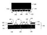
- FIG. 1is a cross-sectional view of an embodiment of a mounting recess for a photonic chip according to the present invention
- FIGS. 2A-Care cross-sectional views showing steps in the fabrication of a recess in a substrate
- FIGS. 3A-Care cross-sectional views showing steps in the fabrication of inclined end faces for a photonic chip
- FIGS. 4A-Eare cross-sectional views showing steps in a wet etching process for forming a recess in a silicon-on-insulator (SOI) substrate;
- FIGS. 5A-Eare cross-sectional views showing steps in a wet etching process for forming inclined end faces on a photonic chip
- FIGS. 6A-Fare cross-sectional views showing steps in fabrication of a recess using a modified SIMOX process
- FIGS. 7A-Care cross-sectional views illustrating control of recess depth in a SOI substrate.
- FIGS. 8A-Bare cross-sectional views illustrating control of recess depth in a silica-on-silicon (SOS) substrate.
- SOSsilica-on-silicon
- FIG. 1is a cross-sectional view of an exemplary embodiment of a photonic chip mounting arrangement according to the present invention.
- Recess 140is formed in top layer 153 and insulating (SiO 2 ) layer 152 of silicon-on-insulator (SOI) or silica-on-silicon (SOS) substrate 150 .
- End walls 130 of recess 140have a nonzero (preferably greater than 10°) inclination angle with respect to vertical; the specific choice of inclination angle will be discussed in more detail below. In some embodiments, all side walls of recess 140 have similarly inclined surfaces, although this is not required.
- Recess 140has a substantially flat bottom surface 141 .
- bottom surface 141has a surface area of about 300 ⁇ m by 300 ⁇ m.
- a number of pillars 160(which may be anywhere from 2 to 50 ⁇ m tall) are formed on bottom surface 141 , each pillar having inclined side faces.
- three pillars 160 in a triangular arrangementare used, but the number and placement of pillars may be varied.
- Conducting paths and pads(not shown) are preferably fabricated on bottom surface 141 for electrical connection with a photonic chip.
- One or more integrated optical waveguidesare fabricated in top layer 153 , which comprises silicon when the substrate is an SOI wafer, or doped silica or glass when the substrate is an SOS wafer.
- the integrated optical waveguidesmay include any optical waveguiding and/or beam-reshaping structure, including a micro-optic structure such as a micro-optical lens, mirror, or diffractive element.
- the waveguidesmay also include a combined waveguiding and beam transformation structure, such as a coupler of the type described in the above-cross-referenced co-pending U.S.
- the integrated optical waveguidesmay be fabricated using any suitable methods and materials, including but not limited to glass, semiconductors, polymers, optical crystals, or other dielectric materials. Fabrication of the waveguides in top layer 153 may be done before, after, or concurrently with formation of recess 140 .
- a photonic integrated circuit (chip) 120has inclined end faces 110 , the inclination angle of which is approximately equal to the inclination of the end walls 130 of recess 140 . Again, in some embodiments, all side faces of photonic chip 120 have similarly inclined surfaces, although this is not required.
- the dimensions of bottom surface 121 of photonic chip 120are substantially equal to the corresponding dimensions of the bottom surface 141 of recess 140 .
- a number of indentations 180typically about 1 to 10 ⁇ m deep
- each indentationaligns with a corresponding pillar 160 on bottom surface 141 of recess 140 so that the top of each pillar 160 fits into one of indentations 180 .
- the respective inclination angles of chip end faces 110 and recess end walls 130provide automatic lateral alignment between the waveguiding region of photonic chip 120 and the integrated optical waveguides fabricated in layer 153 .
- the depth of recess 140is also controlled to provide vertical alignment between the waveguiding region of photonic chip 120 and the integrated optical waveguides fabricated in layer 153 and, if desired, to leave enough space for electrical connection materials.
- pillars 160 and indentations 180provide an enhanced docking mechanism.
- the interlocking of pillars 160 and indentations 180helps to guide photonic chip 120 into position while protecting end faces 110 from mechanical damage.
- pillars 160are made higher than indentation 180 so that bottom surface 121 of photonic chip 120 does not contact bottom surface 141 of recess 140 .
- electrical connection materialssuch as solder materials or silvered epoxy, are placed in the space between surfaces 121 and 141 to fix photonic chip 120 into position and to provide electrical connections for photonic chip 120 .
- pillars 160 and indentations 180also improves the alignment of photonic chip 120 with waveguides fabricated in silicon or glass layer 153 . It will be appreciated that similar docking and alignment functionality may alternatively be provided by indentations in recess 140 and matching pillars on the bottom surface of chip 110 , and that the number and placement of pillars and corresponding indentations may be varied.
- FIGS. 2A-Cillustrate a dry etching process for forming a recess with vertically inclined walls in a silicon-based substrate.
- FIG. 2Ashows a substrate 200 , which may be an SOI or SOS substrate.
- Substrate 200includes a bottom silicon layer 234 , an insulating (SiO 2 ) layer 235 , and a top layer 230 .
- Top layer 230may be either a silicon layer of an SOI wafer or glass waveguide layer on an SOS wafer, the glass waveguide layer having a higher refractive index than insulating layer 235 .
- a photoresist layer 210is applied to top layer 230 , e.g., by spin-coating.
- a grayscale mask 220is then introduced.
- Grayscale mask 220is designed to have a low-density area (shown as a light gray area) in the central recess region, progressively increasing-density areas at the end walls, and a high-density area (shown as a dark area) outside the recess.
- Photolithography with ultraviolet (UV) exposurecauses a portion of photoresist layer 230 to be removed in inverse proportion to the density of grayscale mask 220 .
- photolithography using grayscale mask 220produces a vertically tapered photoresist pattern 215 , shown in FIG. 2B.
- a dry etching processtransfers tapered photoresist pattern 215 to top layer 230 and insulating (SiO 2 ) layer 235 , as shown in FIG. 2 C. This creates a recess region 240 with vertically inclined (or tapered) side walls 250 .
- the grayscale maskis designed so that pillars within the area of the recess are also formed via dry etching. This may be done, for instance, by configuring grayscale mask 220 to provide additional protected (high-density) or partially protected regions within the recess area.
- openings or trenches for conducting paths and/or padsare then formed, for instance by using well-known dry etching techniques.
- Conducting paths and/or padsare then formed by depositing metal film into these openings or trenches, e.g., by evaporation, sputtering or other known processes. This step may be followed by electroplating to increase the thickness of the metal films.
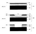
- FIGS. 3A-Cillustrate a dry etching process for forming inclined end faces on a photonic chip.
- a photoresist layer 260is applied to the surface of a photonic chip 280 , e.g., by spin-coating.
- a grayscale mask 270is then used in photolithography to form vertically tapered photoresist pattern 275 , shown in FIG. 3B.
- a dry etching process(indicated by arrows) transfers tapered photoresist pattern 275 to photonic chip 280 . This process defines a photonic chip mounting surface 285 and vertically inclined (or tapered) end faces 290 .
- the width of surface 285is chosen so that when photonic chip 280 is mounted on a substrate, such as substrate 200 (shown in FIG. 2 C), surface 285 fits into recess 240 , and chip end faces 290 align with recess end walls 250 .
- the grayscale mask 270is designed so that indentations in the bottom surface of the photonic chip are also formed via dry etching. This may be done, for instance, by providing additional exposed or partly exposed areas on the grayscale mask.
- An alternative approachuses wet etching rather than dry etching to provide nearly equal inclination angles for the photonic chip and recess at lower cost and complexity. It is well known in the art that Si-, GaAs- and InP-based semiconductors all have crystal planes of different orientations and that highly selective wet etching techniques are capable of revealing these crystal planes, resulting in the formation of angled walls (such as V-grooves) in these semiconductors. The inclination angle of a V-groove side wall with respect to the vertical direction depends on the crystalline structure. For the most commonly used (100) orientation semiconductors, the angles are similar: 35.25° for Si, 35° for GaAs, and 32.5° for InP.
- wet etchingThe disadvantage of wet etching is that the respective inclination angles of the photonic chip end faces and recess side walls will not be exactly equal if different semiconductors are used, e.g., if the recess is formed in a silicon wafer for mounting an InP-based photonic chip. In view of the lower cost of wet etching, however, the differences in inclination angles are small enough to be acceptable for many applications.
- FIGS. 4A-Eillustrate a wet etching process for forming a recess in a (100) SOI wafer 310 .
- Wafer 310shown in FIG. 4A comprises a base silicon layer 311 , an insulating SiO 2 layer 312 , and an upper silicon layer 313 , in which integrated channel waveguides are to be formed.
- a thin (for example, 200 nm) cap layer 320 of SiO 2 and/or Si 3 N 4is deposited on the SOI wafer 310 using, e.g., chemical vapor deposition.
- a photoresist pattern 330is generated on top of cap layer 320 using standard photolithography-based processes.
- Reactive ion etchingis then performed to remove the part of cap layer 320 that is not protected by photoresist pattern 330 .
- the remaining photoresist 330is removed and highly selective wet etching in aqueous potassium hydroxide (KOH) solution is carried out to form the vertically inclined side walls 340 of the recess in waveguide layer 313 , as shown in FIG. 4 D.
- KOHpotassium hydroxide
- the remaining portion of cap pattern 320 and the part of SiO 2 layer 312 occupying the central portion of the recessare then etched away, as shown in FIG. 4E , using highly selective dry or wet etching that does not attack silicon.
- the end wall of the recessmay be vertical in SiO 2 layer 312 , as shown in FIG. 4 E.
- Adequate alignment between waveguide layer 313 and the photonic chipis provided by the inclined part of the wall in the top silicon layer.
- pillarsare also formed in the recess; they can be fabricated during etching of the recess by using a suitably patterned photoresist. If desired, they can be shortened after fabrication by a further etching process in which the side walls of the recess are protected. After formation of the recess, conducting paths and/or pads may be fabricated on the floor of the recess, as described above. It will be appreciated that other materials and etchants may be used in the above-described method.
- FIGS. 5A-DA similar process for wet etching of an InP-based photonic chip 360 is shown in FIGS. 5A-D .
- a thin (for example 100 nm) titanium cap layer 370is applied to photonic chip 360 , using, e.g., e-beam evaporation.
- a photoresist pattern 380is then generated on top of cap layer 370 using standard photolithography-based processes.
- Wet etchingis then performed to remove the part of cap layer 370 that is not protected by photoresist pattern 380 , thereby forming a patterned cap 375 , shown in FIG. 5 B.
- FIG. 5Eshows an example of wet-etched photonic chip 360 mounted in a recess wet-etched in a silicon substrate 332 . Alignment is achieved using pillars and indentations 337 . A small (about 1 ⁇ m) gap 335 remains between photonic chip end face 390 and recess end face 339 . For many applications, gap 335 does not lead to unacceptable light loss.
- a combination of wet and dry etchingmay be used to create the vertically inclined side faces.
- the photonic chipmay be wet etched while the recess is dry etched to match the inclination angle of the photonic chip.
- dry etchingis preferred because glass is an amorphous material rather than a crystal.
- the depth of the recessmust be controlled.
- the process for fabricating a mounting recessprovides flexible control over the depth of the recess so that the process may be used with a broad range of photonic chips having different vertical dimensions. Two methods for flexibly controlling the depth of a recess according to the present invention will now be described. It will be appreciated that these are examples and that other processes may be employed.
- One preferred processemploys a silicon-on-insulator (SOI) wafer in which the depth of the insulating SiO 2 layer is different at different locations in the wafer.
- SOIsilicon-on-insulator
- Such a wafercan be fabricated using a modified Separation by IMplanted Oxygen (SIMOX) process in which the depth of the implanted insulating layer is controlled, as will now be described.
- SIMOXSeparation by IMplanted Oxygen
- SIMOX-based SOI wafersare made by implanting oxygen ions into a silicon wafer, then thermally annealing the wafer to convert the oxygen-ion-implanted region into SiO 2 .
- the depth of the buried SiO 2 layer(which determines the thickness of the top silicon layer) is determined by the ion energy, while the thickness of the buried SiO 2 layer is determined by the range of ion energies used, to create a thicker SiO 2 layer, multiple implantations may be performed, each with a different ion energy.
- the thickness of the top silicon layermay optionally be increased by epitaxially growing silicon upwards.
- Existing SIMOX processesresult in the buried SiO 2 layer and the top silicon layer each having essentially a uniform thickness.
- FIG. 6Ashows a silicon wafer 445 on which a patterned implantation retardation mask 410 , made of, e.g., SiO 2 , has been deposited using plasma-enhanced chemical vapor deposition or other suitable deposition techniques, e.g., thermal oxidation.
- Retardation mask 410is patterned by means of conventional photolithography or related patterning technologies.
- oxygen ion implantation(indicated by arrows 430 ) is then carried out to create buried SiO 2 layers 440 , 450 .
- the thickness of retardation mask 410controls the depth to which the ions will penetrate into silicon wafer 445 . As ions pass through retardation mask 410 , they are slowed and thus enter wafer 445 with less energy than ions that have not passed through retardation mask 410 . Consequently, in the region of mask 410 , ions do not penetrate as far as where mask 410 is absent. Thus implanted SiO 2 layer 450 (where there is no retardation mask) is at a lower depth than implanted SiO 2 layer 440 . As is well known in the art, multiple oxygen ion implantation steps using different ion energies may be used to increase the thickness of implanted SiO 2 layers 440 , 450 .
- wet etching mask 460is created, either by removing part of retardation mask 410 or by completely removing retardation mask 410 and forming a new wet etching mask 460 .
- the silicon region above the deeper buried SiO 2 layer 450is then etched using highly selective wet etching for silicon (indicated by arrows 470 ), resulting in the configuration of FIG. 6 D.
- This stepis followed by either dry or wet etching of SiO 2 to remove the protruding edges of upper buried SiO 2 layer 440 along with lower SiO 2 layer 450 , as shown in FIG. 6 E.
- the SiO 2 /Si interface 455(indicated in FIG. 6D ) provides a natural etch stop; thus, because the modified SIMOX process controls the depth of interface 455 , the depth of recess 465 is controlled.
- Silicon layer 480 above the shallower buried SiO 2 layer 440may be made into small-dimension silicon channel waveguides to form the small-beam-size side of a beam-size transformer as described in the above-cross-referenced co-pending application entitled “Integrated Planar Composite Coupling Structures for Bi-directional Light Beam Transformation between a Small Mode Size Waveguide and a Large Mode Size Waveguide.”
- other waveguidesmay be formed in layer 480 .
- a photonic chip 490 with inclined end facesis mounted in recess 465 , as shown in FIG. 6 F.
- the depth of the recessmay also be controlled by using as a substrate either an SOI wafer made through wafer bonding or an SOS wafer made through thermal oxidation.
- FIG. 7Ashows an SOI wafer 500 comprising bottom silicon layer 505 , insulating layer 510 , and top silicon layer 520 .
- smart cutting technologycombined with wafer bonding processes allow precise control of the thickness of both insulating layer 510 and top silicon layer 520 .
- Etching cap pattern 530shown in FIG. 7B , is created using photolithography-related processes such as metal deposition and lift off, and wet etching is carried out to create vertically inclined end walls 522 for top silicon layer 520 .
- dry etching of SiO 2is performed, which provides a natural stop at an SiO 2 /Si interface 527 .
- FIG. 7CA section of the recess end wall is vertical, but as discussed above with reference to FIG. 4E , adequate alignment and docking is still provided by inclined end faces 522 and preferably the fabrication of pillars (not shown). Because the thickness of top silicon layer 520 and insulating layer 510 may be precisely controlled during wafer fabrication, flexible control over the depth of the recess is provided.
- FIG. 8illustrates control of the recess depth in an SOS wafer.
- FIG. 8Ashows an SOS wafer having a top glass waveguide layer 640 over SiO 2 layer 610 .
- such waferscan be made through thermal oxidation, followed by deposition of the waveguide layer 640 , which provides good control over the thickness of top layer 640 and SiO 2 layer 610 .
- a grayscale-mask-created photoresist pattern 650is formed on the wafer, and dry etching 660 is employed to create the inclined side walls 680 of the recess 670 .
- the detailsare similar to those described above with regard to FIG. 2 , with the SiO 2 /Si interface 827 serving as a natural etch stop.
- the thickness of top glass waveguide layer 640 and SiO 2 layer 610may be precisely controlled during wafer fabrication, enhanced control over the depth of the recess is provided.
- the exemplary embodimentsemploy a silicon substrate, other suitable materials may be used, for instance InP, GaAs, LiNbO 3 and BaTiO 3 .
- the representative dimensions provided hereinare exemplary and may be varied.
- integrated beam-size-transformation couplershave been used as exemplary integrated waveguides, the present invention may be used with any other type of integrated channel waveguide or other optical device, including waveguide-based lasers, amplifiers, modulators, or photodetectors.
Landscapes
- Physics & Mathematics (AREA)
- General Physics & Mathematics (AREA)
- Optics & Photonics (AREA)
- Optical Integrated Circuits (AREA)
- Optical Couplings Of Light Guides (AREA)
Abstract
Description
Claims (12)
Priority Applications (1)
| Application Number | Priority Date | Filing Date | Title |
|---|---|---|---|
| US10/310,604US6888989B1 (en) | 2001-12-11 | 2002-12-04 | Photonic chip mounting in a recess for waveguide alignment and connection |
Applications Claiming Priority (2)
| Application Number | Priority Date | Filing Date | Title |
|---|---|---|---|
| US33913101P | 2001-12-11 | 2001-12-11 | |
| US10/310,604US6888989B1 (en) | 2001-12-11 | 2002-12-04 | Photonic chip mounting in a recess for waveguide alignment and connection |
Publications (1)
| Publication Number | Publication Date |
|---|---|
| US6888989B1true US6888989B1 (en) | 2005-05-03 |
Family
ID=34525925
Family Applications (1)
| Application Number | Title | Priority Date | Filing Date |
|---|---|---|---|
| US10/310,604Expired - Fee RelatedUS6888989B1 (en) | 2001-12-11 | 2002-12-04 | Photonic chip mounting in a recess for waveguide alignment and connection |
Country Status (1)
| Country | Link |
|---|---|
| US (1) | US6888989B1 (en) |
Cited By (39)
| Publication number | Priority date | Publication date | Assignee | Title |
|---|---|---|---|---|
| US20040042729A1 (en)* | 2002-08-28 | 2004-03-04 | Phosistor Technologies, Inc. | Optical beam transformer module for light coupling between a fiber array and a photonic chip and the method of making the same |
| US20050014300A1 (en)* | 2001-10-09 | 2005-01-20 | Infinera Corporation | Optical probe and method of testing employing an interrogation beam or optical pickup |
| US20050036738A1 (en)* | 2002-08-28 | 2005-02-17 | Phosistor Technologies, Inc. | Varying refractive index optical medium using at least two materials with thicknesses less than a wavelength |
| US20090141224A1 (en)* | 2007-11-29 | 2009-06-04 | Sony Corporation | Photosensor and display device |
| US20090170232A1 (en)* | 2007-12-27 | 2009-07-02 | Joon-Ku Yoon | Method for manufacturing iamge sensor |
| US20100135615A1 (en)* | 2002-08-28 | 2010-06-03 | Seng-Tiong Ho | Apparatus for coupling light between input and output waveguides |
| CN102983119A (en)* | 2012-11-22 | 2013-03-20 | 华中科技大学 | Recessed type alignment mark used for electron beam alignment on SOI (Silicon On Insulator) and manufacturing method thereof |
| EP1860474B1 (en)* | 2006-05-25 | 2014-10-15 | Xyratex Technology Limited | An optical printed circuit board blank, a kit and a method of making an optical printed circuit board |
| WO2014176561A1 (en)* | 2013-04-25 | 2014-10-30 | Skorpios Technologies, Inc. | Method and system for height registration during chip bonding |
| US9316785B2 (en) | 2013-10-09 | 2016-04-19 | Skorpios Technologies, Inc. | Integration of an unprocessed, direct-bandgap chip into a silicon photonic device |
| US20160291265A1 (en)* | 2015-04-01 | 2016-10-06 | Coriant Advanced Technology, LLC | Optically Aligned Hybrid Semiconductor Device and Method |
| US9496431B2 (en) | 2013-10-09 | 2016-11-15 | Skorpios Technologies, Inc. | Coplanar integration of a direct-bandgap chip into a silicon photonic device |
| US20170254954A1 (en)* | 2016-03-01 | 2017-09-07 | Futurewei Technologies, Inc. | Integration of V-grooves on Silicon-On-Insulator (SOI) Platform for Direct Fiber Coupling |
| US9759868B2 (en) | 2015-11-05 | 2017-09-12 | International Business Machines Corporation | Structures for preventing dicing damage |
| US9829631B2 (en) | 2015-04-20 | 2017-11-28 | Skorpios Technologies, Inc. | Vertical output couplers for photonic devices |
| US9885832B2 (en) | 2014-05-27 | 2018-02-06 | Skorpios Technologies, Inc. | Waveguide mode expander using amorphous silicon |
| US9977188B2 (en) | 2011-08-30 | 2018-05-22 | Skorpios Technologies, Inc. | Integrated photonics mode expander |
| US10088629B2 (en) | 2014-03-07 | 2018-10-02 | Skorpios Technologies, Inc. | Wide shoulder, high order mode filter for thick-silicon waveguides |
| US20180358778A1 (en)* | 2017-06-09 | 2018-12-13 | International Business Machines Corporation | Self-alignment features for iii-v ridge process and angled facet die |
| US10319693B2 (en) | 2014-06-16 | 2019-06-11 | Skorpios Technologies, Inc. | Micro-pillar assisted semiconductor bonding |
| US10393962B2 (en) | 2017-11-30 | 2019-08-27 | International Business Machines Corporation | Optimized stand-offs and mechanical stops for precise three dimensional self-alignment |
| US10649148B2 (en) | 2017-10-25 | 2020-05-12 | Skorpios Technologies, Inc. | Multistage spot size converter in silicon photonics |
| CN111458809A (en)* | 2019-01-22 | 2020-07-28 | 意法半导体(克洛尔2)公司 | Photonic system and method of making the same |
| DE102019213097A1 (en)* | 2019-08-30 | 2021-03-04 | Robert Bosch Gmbh | Process for the production of a photonic system and photonic system |
| JP2021071647A (en)* | 2019-10-31 | 2021-05-06 | 京セラ株式会社 | Optical waveguide package and light emitting device |
| US11183492B2 (en)* | 2010-12-08 | 2021-11-23 | Skorpios Technologies, Inc. | Multilevel template assisted wafer bonding |
| US11181688B2 (en) | 2009-10-13 | 2021-11-23 | Skorpios Technologies, Inc. | Integration of an unprocessed, direct-bandgap chip into a silicon photonic device |
| WO2021250098A1 (en)* | 2020-06-09 | 2021-12-16 | Rockley Photonics Limited | Optoelectronic device and method of manufacture thereof |
| CN113874983A (en)* | 2019-05-15 | 2021-12-31 | 应用材料公司 | Methods of forming variable depth device structures |
| US11360263B2 (en) | 2019-01-31 | 2022-06-14 | Skorpios Technologies. Inc. | Self-aligned spot size converter |
| CN114664863A (en)* | 2020-12-23 | 2022-06-24 | 格芯(美国)集成电路科技有限公司 | Silicon-on-insulator chip structure with substrate-embedded optical waveguides and method |
| WO2022165900A1 (en)* | 2021-02-08 | 2022-08-11 | 桂林雷光科技有限公司 | Semiconductor active and passive integrated coupling method |
| US11482513B2 (en) | 2009-10-13 | 2022-10-25 | Skorpios Technologies, Inc. | Heterogeneous substrate bonding for photonic integration |
| WO2022254290A1 (en) | 2021-05-31 | 2022-12-08 | Picadvanced S.A. | Multifunctional self-sustained hosting apparatus and related bidirectional optical sub assembly based on photonic integrated circuit |
| US11650381B1 (en) | 2022-02-12 | 2023-05-16 | Globalfoundries U.S. Inc. | PIC die and package with cover for multiple level and multiple depth connections of fibers to on-chip optical components |
| US20230228940A1 (en)* | 2022-01-17 | 2023-07-20 | Globalfoundries U.S. Inc. | Photonics chips including cavities with non-right-angle internal corners |
| US12130470B2 (en) | 2021-10-25 | 2024-10-29 | Globalfoundries U.S. Inc. | PIC die and package with multiple level and multiple depth connections of fibers to on-chip optical components |
| US20250110271A1 (en)* | 2023-09-29 | 2025-04-03 | Taiwan Semiconductor Manufacturing Company Ltd | Photonic device and method of fabricating same |
| US12444723B2 (en) | 2022-09-20 | 2025-10-14 | Skorpios Technologies, Inc. | Heterogeneous bonding for photonic integration |
Citations (10)
| Publication number | Priority date | Publication date | Assignee | Title |
|---|---|---|---|---|
| US4466696A (en) | 1982-03-29 | 1984-08-21 | Honeywell Inc. | Self-aligned coupling of optical fiber to semiconductor laser or LED |
| US5259049A (en) | 1991-09-19 | 1993-11-02 | International Business Machines Corporation | Self-aligned optical waveguide to laser structure and method for making the same |
| US5337398A (en) | 1992-11-30 | 1994-08-09 | At&T Bell Laboratories | Single in-line optical package |
| US5444805A (en) | 1992-03-07 | 1995-08-22 | Robert Bosch Gmbh | Integrated optical component |
| US5881190A (en) | 1996-05-16 | 1999-03-09 | Bookham Technology Limited | Assembly of an optical component and an optical waveguide |
| US5907649A (en) | 1994-09-26 | 1999-05-25 | Siemens Aktiengesellschaft | Coupling arrangement for optically coupling together an OEIC module and optical fibers |
| US5937124A (en) | 1996-02-29 | 1999-08-10 | The Whitaker Corporation | Package for an optoelectronic device |
| US6112001A (en) | 1997-07-30 | 2000-08-29 | Kyocera Corporation | Optical coupler and a method of producing it |
| US6151430A (en)* | 1998-07-08 | 2000-11-21 | Gore Enterprise Holdings, Inc. | Photonic device having an integal guide and method of manufacturing |
| US6324323B1 (en)* | 1999-01-07 | 2001-11-27 | Nu-Wave Photonics Inc. | Adhesive-free lens-attached optical fibers to optical waveguide packaging system |
- 2002
- 2002-12-04USUS10/310,604patent/US6888989B1/ennot_activeExpired - Fee Related
Patent Citations (10)
| Publication number | Priority date | Publication date | Assignee | Title |
|---|---|---|---|---|
| US4466696A (en) | 1982-03-29 | 1984-08-21 | Honeywell Inc. | Self-aligned coupling of optical fiber to semiconductor laser or LED |
| US5259049A (en) | 1991-09-19 | 1993-11-02 | International Business Machines Corporation | Self-aligned optical waveguide to laser structure and method for making the same |
| US5444805A (en) | 1992-03-07 | 1995-08-22 | Robert Bosch Gmbh | Integrated optical component |
| US5337398A (en) | 1992-11-30 | 1994-08-09 | At&T Bell Laboratories | Single in-line optical package |
| US5907649A (en) | 1994-09-26 | 1999-05-25 | Siemens Aktiengesellschaft | Coupling arrangement for optically coupling together an OEIC module and optical fibers |
| US5937124A (en) | 1996-02-29 | 1999-08-10 | The Whitaker Corporation | Package for an optoelectronic device |
| US5881190A (en) | 1996-05-16 | 1999-03-09 | Bookham Technology Limited | Assembly of an optical component and an optical waveguide |
| US6112001A (en) | 1997-07-30 | 2000-08-29 | Kyocera Corporation | Optical coupler and a method of producing it |
| US6151430A (en)* | 1998-07-08 | 2000-11-21 | Gore Enterprise Holdings, Inc. | Photonic device having an integal guide and method of manufacturing |
| US6324323B1 (en)* | 1999-01-07 | 2001-11-27 | Nu-Wave Photonics Inc. | Adhesive-free lens-attached optical fibers to optical waveguide packaging system |
Non-Patent Citations (2)
| Title |
|---|
| Boyd, et al., "Optical Coupling from Fibers to Channel Waveguides Formed on Silicon," Applied Optics, vol. 17, No. 6, Optical Society of America, pp. 895-898, (Mar. 15, 1978). |
| Choi, et al., "Self-Aligning Silicon Groove Technology Platform for the Low Cost Optical Module," Electronic Components and Technology Conference, pp. 1140-1144, (1999). |
Cited By (74)
| Publication number | Priority date | Publication date | Assignee | Title |
|---|---|---|---|---|
| US7079718B2 (en)* | 2001-10-09 | 2006-07-18 | Infinera Corporation | Optical probe and method of testing employing an interrogation beam or optical pickup |
| US20050014300A1 (en)* | 2001-10-09 | 2005-01-20 | Infinera Corporation | Optical probe and method of testing employing an interrogation beam or optical pickup |
| US20040042729A1 (en)* | 2002-08-28 | 2004-03-04 | Phosistor Technologies, Inc. | Optical beam transformer module for light coupling between a fiber array and a photonic chip and the method of making the same |
| US20050036738A1 (en)* | 2002-08-28 | 2005-02-17 | Phosistor Technologies, Inc. | Varying refractive index optical medium using at least two materials with thicknesses less than a wavelength |
| US7303339B2 (en) | 2002-08-28 | 2007-12-04 | Phosistor Technologies, Inc. | Optical beam transformer module for light coupling between a fiber array and a photonic chip and the method of making the same |
| US7426328B2 (en) | 2002-08-28 | 2008-09-16 | Phosistor Technologies, Inc. | Varying refractive index optical medium using at least two materials with thicknesses less than a wavelength |
| US20090046979A1 (en)* | 2002-08-28 | 2009-02-19 | Phosistor Technologies, Inc. | Varying refractive index optical medium using at least two materials with thicknesses less than a wavelength |
| US8538208B2 (en) | 2002-08-28 | 2013-09-17 | Seng-Tiong Ho | Apparatus for coupling light between input and output waveguides |
| US7616856B2 (en)* | 2002-08-28 | 2009-11-10 | Phosistor Technologies, Inc. | Varying refractive index optical medium using at least two materials with thicknesses less than a wavelength |
| US20100135615A1 (en)* | 2002-08-28 | 2010-06-03 | Seng-Tiong Ho | Apparatus for coupling light between input and output waveguides |
| EP1860474B1 (en)* | 2006-05-25 | 2014-10-15 | Xyratex Technology Limited | An optical printed circuit board blank, a kit and a method of making an optical printed circuit board |
| TWI397173B (en)* | 2007-11-29 | 2013-05-21 | Japan Display West Inc | Photoreceptor and display device |
| US20090141224A1 (en)* | 2007-11-29 | 2009-06-04 | Sony Corporation | Photosensor and display device |
| US7787082B2 (en)* | 2007-11-29 | 2010-08-31 | Sony Corporation | Photosensor and display device |
| US20090170232A1 (en)* | 2007-12-27 | 2009-07-02 | Joon-Ku Yoon | Method for manufacturing iamge sensor |
| US11482513B2 (en) | 2009-10-13 | 2022-10-25 | Skorpios Technologies, Inc. | Heterogeneous substrate bonding for photonic integration |
| US12287510B2 (en)* | 2009-10-13 | 2025-04-29 | Skorpios Technologies, Inc. | Integration of an unprocessed, direct-bandgap chip into a silicon photonic device |
| US20220171125A1 (en)* | 2009-10-13 | 2022-06-02 | Skorpios Technologies, Inc. | Integration of an unprocessed, direct-bandgap chip into a silicon photonic device |
| US11181688B2 (en) | 2009-10-13 | 2021-11-23 | Skorpios Technologies, Inc. | Integration of an unprocessed, direct-bandgap chip into a silicon photonic device |
| US11183492B2 (en)* | 2010-12-08 | 2021-11-23 | Skorpios Technologies, Inc. | Multilevel template assisted wafer bonding |
| US9977188B2 (en) | 2011-08-30 | 2018-05-22 | Skorpios Technologies, Inc. | Integrated photonics mode expander |
| US10895686B2 (en) | 2011-08-30 | 2021-01-19 | Skorpios Technologies, Inc. | Integrated photonics mode expander |
| CN102983119B (en)* | 2012-11-22 | 2015-08-26 | 华中科技大学 | The upper recessed alignment marks for electron beam alignment of SOI and manufacture method |
| CN102983119A (en)* | 2012-11-22 | 2013-03-20 | 华中科技大学 | Recessed type alignment mark used for electron beam alignment on SOI (Silicon On Insulator) and manufacturing method thereof |
| WO2014176561A1 (en)* | 2013-04-25 | 2014-10-30 | Skorpios Technologies, Inc. | Method and system for height registration during chip bonding |
| US9324682B2 (en) | 2013-04-25 | 2016-04-26 | Skorpios Technologies, Inc. | Method and system for height registration during chip bonding |
| US9316785B2 (en) | 2013-10-09 | 2016-04-19 | Skorpios Technologies, Inc. | Integration of an unprocessed, direct-bandgap chip into a silicon photonic device |
| US9882073B2 (en) | 2013-10-09 | 2018-01-30 | Skorpios Technologies, Inc. | Structures for bonding a direct-bandgap chip to a silicon photonic device |
| US9923105B2 (en) | 2013-10-09 | 2018-03-20 | Skorpios Technologies, Inc. | Processing of a direct-bandgap chip after bonding to a silicon photonic device |
| US9496431B2 (en) | 2013-10-09 | 2016-11-15 | Skorpios Technologies, Inc. | Coplanar integration of a direct-bandgap chip into a silicon photonic device |
| US10088629B2 (en) | 2014-03-07 | 2018-10-02 | Skorpios Technologies, Inc. | Wide shoulder, high order mode filter for thick-silicon waveguides |
| US10295746B2 (en) | 2014-03-07 | 2019-05-21 | Skorpios Technologies, Inc. | Wide shoulder, high order mode filter for thick-silicon waveguides |
| US9885832B2 (en) | 2014-05-27 | 2018-02-06 | Skorpios Technologies, Inc. | Waveguide mode expander using amorphous silicon |
| US11409039B2 (en) | 2014-05-27 | 2022-08-09 | Skorpios Technologies, Inc. | Waveguide mode expander having non-crystalline silicon features |
| US10001600B2 (en) | 2014-05-27 | 2018-06-19 | Skorpios Technologies, Inc. | Waveguide mode expander having an amorphous-silicon shoulder |
| US10345521B2 (en) | 2014-05-27 | 2019-07-09 | Skorpios Technologies, Inc. | Method of modifying mode size of an optical beam, using a waveguide mode expander having non-crystalline silicon features |
| US10319693B2 (en) | 2014-06-16 | 2019-06-11 | Skorpios Technologies, Inc. | Micro-pillar assisted semiconductor bonding |
| US10222565B2 (en) | 2015-04-01 | 2019-03-05 | Elenion Technologies, Llc | Optically aligned hybrid semiconductor device and method |
| US20160291265A1 (en)* | 2015-04-01 | 2016-10-06 | Coriant Advanced Technology, LLC | Optically Aligned Hybrid Semiconductor Device and Method |
| US20190179091A1 (en)* | 2015-04-01 | 2019-06-13 | Elenion Technologies, Llc | Optically aligned hybrid semiconductor device and method |
| US9817197B2 (en)* | 2015-04-01 | 2017-11-14 | Elenion Technologies, Llc | Optically aligned hybrid semiconductor device and method |
| WO2016161150A1 (en)* | 2015-04-01 | 2016-10-06 | Coriant Advanced Technology, LLC | Optically aligned hybrid semiconductor device and method |
| US10678005B2 (en)* | 2015-04-01 | 2020-06-09 | Elenion Technologies, Llc | Optically aligned hybrid semiconductor device and method |
| US10132996B2 (en) | 2015-04-20 | 2018-11-20 | Skorpios Technologies, Inc. | Back side via vertical output couplers |
| US9829631B2 (en) | 2015-04-20 | 2017-11-28 | Skorpios Technologies, Inc. | Vertical output couplers for photonic devices |
| US9759868B2 (en) | 2015-11-05 | 2017-09-12 | International Business Machines Corporation | Structures for preventing dicing damage |
| US20170254954A1 (en)* | 2016-03-01 | 2017-09-07 | Futurewei Technologies, Inc. | Integration of V-grooves on Silicon-On-Insulator (SOI) Platform for Direct Fiber Coupling |
| US9933570B2 (en)* | 2016-03-01 | 2018-04-03 | Futurewei Technologies, Inc. | Integration of V-grooves on silicon-on-insulator (SOI) platform for direct fiber coupling |
| US20180358778A1 (en)* | 2017-06-09 | 2018-12-13 | International Business Machines Corporation | Self-alignment features for iii-v ridge process and angled facet die |
| US11239631B2 (en) | 2017-06-09 | 2022-02-01 | International Business Machines Corporation | Self-alignment features for III-V ridge process and angled facet die |
| US10490971B2 (en) | 2017-06-09 | 2019-11-26 | International Business Machines Corporation | Self-alignment features for III-V ridge process and angled facet die |
| US10649148B2 (en) | 2017-10-25 | 2020-05-12 | Skorpios Technologies, Inc. | Multistage spot size converter in silicon photonics |
| US11079549B2 (en) | 2017-10-25 | 2021-08-03 | Skorpios Technologies, Inc. | Multistage spot size converter in silicon photonics |
| US10393962B2 (en) | 2017-11-30 | 2019-08-27 | International Business Machines Corporation | Optimized stand-offs and mechanical stops for precise three dimensional self-alignment |
| US12019293B2 (en) | 2019-01-22 | 2024-06-25 | Stmicroelectronics (Crolles 2) Sas | Photonic system and method for its manufacture |
| CN111458809A (en)* | 2019-01-22 | 2020-07-28 | 意法半导体(克洛尔2)公司 | Photonic system and method of making the same |
| US11474317B2 (en) | 2019-01-22 | 2022-10-18 | Stmicroelectronics (Crolles 2) Sas | Photonic system and method for its manufacture |
| CN111458809B (en)* | 2019-01-22 | 2022-07-26 | 意法半导体(克洛尔2)公司 | Photonic system and method of making the same |
| US11360263B2 (en) | 2019-01-31 | 2022-06-14 | Skorpios Technologies. Inc. | Self-aligned spot size converter |
| CN113874983A (en)* | 2019-05-15 | 2021-12-31 | 应用材料公司 | Methods of forming variable depth device structures |
| DE102019213097A1 (en)* | 2019-08-30 | 2021-03-04 | Robert Bosch Gmbh | Process for the production of a photonic system and photonic system |
| JP2021071647A (en)* | 2019-10-31 | 2021-05-06 | 京セラ株式会社 | Optical waveguide package and light emitting device |
| WO2021250098A1 (en)* | 2020-06-09 | 2021-12-16 | Rockley Photonics Limited | Optoelectronic device and method of manufacture thereof |
| US12313878B2 (en) | 2020-06-09 | 2025-05-27 | Rockley Photonics Limited | Optoelectronic device and method of manufacture thereof |
| CN114664863A (en)* | 2020-12-23 | 2022-06-24 | 格芯(美国)集成电路科技有限公司 | Silicon-on-insulator chip structure with substrate-embedded optical waveguides and method |
| WO2022165900A1 (en)* | 2021-02-08 | 2022-08-11 | 桂林雷光科技有限公司 | Semiconductor active and passive integrated coupling method |
| WO2022254290A1 (en) | 2021-05-31 | 2022-12-08 | Picadvanced S.A. | Multifunctional self-sustained hosting apparatus and related bidirectional optical sub assembly based on photonic integrated circuit |
| KR20240014497A (en) | 2021-05-31 | 2024-02-01 | 픽어드밴스드 에스.에이. | Photonic integrated circuit-based multifunctional self-sustaining hosting device and associated bidirectional optical subassembly |
| US12130470B2 (en) | 2021-10-25 | 2024-10-29 | Globalfoundries U.S. Inc. | PIC die and package with multiple level and multiple depth connections of fibers to on-chip optical components |
| US20230228940A1 (en)* | 2022-01-17 | 2023-07-20 | Globalfoundries U.S. Inc. | Photonics chips including cavities with non-right-angle internal corners |
| US11828983B2 (en)* | 2022-01-17 | 2023-11-28 | Globalfoundries U.S. Inc. | Photonics chips including cavities with non-right-angle internal corners |
| US11650381B1 (en) | 2022-02-12 | 2023-05-16 | Globalfoundries U.S. Inc. | PIC die and package with cover for multiple level and multiple depth connections of fibers to on-chip optical components |
| US12444723B2 (en) | 2022-09-20 | 2025-10-14 | Skorpios Technologies, Inc. | Heterogeneous bonding for photonic integration |
| US20250110271A1 (en)* | 2023-09-29 | 2025-04-03 | Taiwan Semiconductor Manufacturing Company Ltd | Photonic device and method of fabricating same |
Similar Documents
| Publication | Publication Date | Title |
|---|---|---|
| US6888989B1 (en) | Photonic chip mounting in a recess for waveguide alignment and connection | |
| EP3308206B1 (en) | Self-alignment for apparatus comprising photonic device | |
| US11378751B2 (en) | Laser patterned adapters with waveguides and etched connectors for low cost alignment of optics to chips | |
| US6316281B1 (en) | Method for fabricating a hybrid optical integrated circuit employing SOI optical waveguide | |
| US6993225B2 (en) | Tapered structure for providing coupling between external optical device and planar optical waveguide and method of forming the same | |
| US6549713B1 (en) | Stabilized and integrated fiber devices | |
| US9494741B2 (en) | Apparatus comprising at least one optical device optically coupled to at least one waveguide on an optical chip | |
| KR101258725B1 (en) | Wideband optical coupling into thin soi cmos photonic integrated circuit | |
| US20040114869A1 (en) | Mode converter including tapered waveguide for optically coupling photonic devices | |
| US20030019838A1 (en) | Optoelectronic packaging | |
| US8137572B2 (en) | Reflective planar lightwave circuit waveguide | |
| EP3724705B1 (en) | Passive fiber coupler with uv windows | |
| US12019270B2 (en) | Multi-layer silicon photonics apparatus | |
| US7574077B2 (en) | Optical imaging device for optical proximity communication | |
| US20180081207A1 (en) | Edge construction on optical devices | |
| CN113534337A (en) | Processing method and structure of silicon photonic chip optical coupling structure | |
| US20070075443A1 (en) | Resonator system for optical proximity communication | |
| US20020071636A1 (en) | Method and apparatus for attaching an optical fibre to an optical device | |
| EP3414806B1 (en) | Broadband back mirror for a iii-v chip in silicon photonics | |
| WO2004088715A2 (en) | Tapered structure for providing coupling between external optical device and planar optical waveguide and method of forming the same | |
| JP2820202B2 (en) | Manufacturing method of spot size converter | |
| JP2003302545A (en) | Optical transmission module |
Legal Events
| Date | Code | Title | Description |
|---|---|---|---|
| AS | Assignment | Owner name:PHOSISTOR TECHNOLOGIES, INCORPORATED, CALIFORNIA Free format text:ASSIGNMENT OF ASSIGNORS INTEREST;ASSIGNORS:ZHOU, YAN;HO, SENG-TIONG;REEL/FRAME:014001/0362 Effective date:20021122 | |
| FEPP | Fee payment procedure | Free format text:PAYOR NUMBER ASSIGNED (ORIGINAL EVENT CODE: ASPN); ENTITY STATUS OF PATENT OWNER: SMALL ENTITY | |
| AS | Assignment | Owner name:PHOSISTOR TECHNOLOGIES, INC., CALIFORNIA Free format text:ASSIGNMENT OF ASSIGNORS INTEREST;ASSIGNORS:ZHOU, YAN;HO, SENG-TIONG;REEL/FRAME:014651/0761;SIGNING DATES FROM 20030801 TO 20030804 | |
| FPAY | Fee payment | Year of fee payment:4 | |
| FPAY | Fee payment | Year of fee payment:8 | |
| AS | Assignment | Owner name:HO, SENG-TIONG, ILLINOIS Free format text:ASSIGNMENT OF ASSIGNORS INTEREST;ASSIGNOR:PHOSISTOR TECHNOLOGIES, INC.;REEL/FRAME:032037/0903 Effective date:20030828 | |
| REMI | Maintenance fee reminder mailed | ||
| LAPS | Lapse for failure to pay maintenance fees | ||
| STCH | Information on status: patent discontinuation | Free format text:PATENT EXPIRED DUE TO NONPAYMENT OF MAINTENANCE FEES UNDER 37 CFR 1.362 | |
| FP | Lapsed due to failure to pay maintenance fee | Effective date:20170503 |