US6888750B2 - Nonvolatile memory on SOI and compound semiconductor substrates and method of fabrication - Google Patents
Nonvolatile memory on SOI and compound semiconductor substrates and method of fabricationDownload PDFInfo
- Publication number
- US6888750B2 US6888750B2US09/927,642US92764201AUS6888750B2US 6888750 B2US6888750 B2US 6888750B2US 92764201 AUS92764201 AUS 92764201AUS 6888750 B2US6888750 B2US 6888750B2
- Authority
- US
- United States
- Prior art keywords
- array
- layer
- rail
- substrate
- charge storage
- Prior art date
- Legal status (The legal status is an assumption and is not a legal conclusion. Google has not performed a legal analysis and makes no representation as to the accuracy of the status listed.)
- Expired - Lifetime, expires
Links
Images


Classifications
- H—ELECTRICITY
- H10—SEMICONDUCTOR DEVICES; ELECTRIC SOLID-STATE DEVICES NOT OTHERWISE PROVIDED FOR
- H10B—ELECTRONIC MEMORY DEVICES
- H10B43/00—EEPROM devices comprising charge-trapping gate insulators
- H10B43/30—EEPROM devices comprising charge-trapping gate insulators characterised by the memory core region
- H—ELECTRICITY
- H10—SEMICONDUCTOR DEVICES; ELECTRIC SOLID-STATE DEVICES NOT OTHERWISE PROVIDED FOR
- H10B—ELECTRONIC MEMORY DEVICES
- H10B41/00—Electrically erasable-and-programmable ROM [EEPROM] devices comprising floating gates
- H10B41/20—Electrically erasable-and-programmable ROM [EEPROM] devices comprising floating gates characterised by three-dimensional arrangements, e.g. with cells on different height levels
- H—ELECTRICITY
- H10—SEMICONDUCTOR DEVICES; ELECTRIC SOLID-STATE DEVICES NOT OTHERWISE PROVIDED FOR
- H10B—ELECTRONIC MEMORY DEVICES
- H10B41/00—Electrically erasable-and-programmable ROM [EEPROM] devices comprising floating gates
- H10B41/30—Electrically erasable-and-programmable ROM [EEPROM] devices comprising floating gates characterised by the memory core region
- H—ELECTRICITY
- H10—SEMICONDUCTOR DEVICES; ELECTRIC SOLID-STATE DEVICES NOT OTHERWISE PROVIDED FOR
- H10B—ELECTRONIC MEMORY DEVICES
- H10B43/00—EEPROM devices comprising charge-trapping gate insulators
- H10B43/20—EEPROM devices comprising charge-trapping gate insulators characterised by three-dimensional arrangements, e.g. with cells on different height levels
- H—ELECTRICITY
- H10—SEMICONDUCTOR DEVICES; ELECTRIC SOLID-STATE DEVICES NOT OTHERWISE PROVIDED FOR
- H10B—ELECTRONIC MEMORY DEVICES
- H10B69/00—Erasable-and-programmable ROM [EPROM] devices not provided for in groups H10B41/00 - H10B63/00, e.g. ultraviolet erasable-and-programmable ROM [UVEPROM] devices
- H—ELECTRICITY
- H10—SEMICONDUCTOR DEVICES; ELECTRIC SOLID-STATE DEVICES NOT OTHERWISE PROVIDED FOR
- H10D—INORGANIC ELECTRIC SEMICONDUCTOR DEVICES
- H10D84/00—Integrated devices formed in or on semiconductor substrates that comprise only semiconducting layers, e.g. on Si wafers or on GaAs-on-Si wafers
- H10D84/01—Manufacture or treatment
- H10D84/02—Manufacture or treatment characterised by using material-based technologies
- H10D84/03—Manufacture or treatment characterised by using material-based technologies using Group IV technology, e.g. silicon technology or silicon-carbide [SiC] technology
- H10D84/038—Manufacture or treatment characterised by using material-based technologies using Group IV technology, e.g. silicon technology or silicon-carbide [SiC] technology using silicon technology, e.g. SiGe
- H—ELECTRICITY
- H10—SEMICONDUCTOR DEVICES; ELECTRIC SOLID-STATE DEVICES NOT OTHERWISE PROVIDED FOR
- H10D—INORGANIC ELECTRIC SEMICONDUCTOR DEVICES
- H10D86/00—Integrated devices formed in or on insulating or conducting substrates, e.g. formed in silicon-on-insulator [SOI] substrates or on stainless steel or glass substrates
- H10D86/01—Manufacture or treatment
- G—PHYSICS
- G11—INFORMATION STORAGE
- G11C—STATIC STORES
- G11C16/00—Erasable programmable read-only memories
- G11C16/02—Erasable programmable read-only memories electrically programmable
- G11C16/04—Erasable programmable read-only memories electrically programmable using variable threshold transistors, e.g. FAMOS
- G11C16/0466—Erasable programmable read-only memories electrically programmable using variable threshold transistors, e.g. FAMOS comprising cells with charge storage in an insulating layer, e.g. metal-nitride-oxide-silicon [MNOS], silicon-oxide-nitride-oxide-silicon [SONOS]
- H—ELECTRICITY
- H10—SEMICONDUCTOR DEVICES; ELECTRIC SOLID-STATE DEVICES NOT OTHERWISE PROVIDED FOR
- H10D—INORGANIC ELECTRIC SEMICONDUCTOR DEVICES
- H10D88/00—Three-dimensional [3D] integrated devices
- H—ELECTRICITY
- H10—SEMICONDUCTOR DEVICES; ELECTRIC SOLID-STATE DEVICES NOT OTHERWISE PROVIDED FOR
- H10D—INORGANIC ELECTRIC SEMICONDUCTOR DEVICES
- H10D88/00—Three-dimensional [3D] integrated devices
- H10D88/01—Manufacture or treatment
Definitions
- the present inventionis directed generally to semiconductor devices and methods of fabrication and more particularly to a nonvolatile memory array and method of fabrication.
- driver circuitsalso known as peripheral circuits
- driver circuitsalso known as peripheral circuits
- Such a memory arrayis disclosed in U.S. Pat. Nos. 6,034,882 and 6,185,122, incorporated herein by reference.
- forming the driver circuits in the bulk monocrystalline silicon substratemay be undesirable for some applications of the memory array.
- a preferred embodiment of the present inventionprovides a nonvolatile memory array, comprising an array of nonvolatile memory devices, at least one driver circuit, and a substrate, wherein the at least one driver circuit is not located in a bulk monocrystalline silicon substrate.
- Nonvolatile memory arraycomprising a monocrystalline silicon substrate, at least one driver circuit formed above the substrate, and an array of nonvolatile memory devices formed above the substrate.
- Another preferred embodiment of the present inventionprovides a method of making a nonvolatile memory array, comprising forming at least one driver circuit above a substrate or in a semiconductor substrate other than a monocrystalline silicon substrate, and forming an array of nonvolatile memory devices.
- FIGS. 1-3are schematic side cross sectional views of a memory array according to the first and second preferred embodiments of the invention.
- FIG. 4Ais a three dimensional view of a rail stack antifuse memory array according to the third preferred embodiment of the invention.
- FIG. 4Bis a side cross sectional view of a rail stack antifuse memory array according to an alternative aspect of the third preferred embodiment of the invention.
- FIG. 5is a three dimensional view of a rail stack EEPROM memory array according to the fourth preferred embodiment of the invention.
- FIGS. 6 and 7are three dimensional views of two terminal pillar devices according to the fifth preferred embodiment of the invention.
- FIG. 8is a three dimensional view of an EEPROM pillar device according to the sixth preferred embodiment of the invention.
- FIG. 9is a three dimensional view of an TFT EEPROM array according to the seventh preferred embodiment of the invention.
- FIG. 10Ais side cross sectional view of an FN tunneling flash memory array according to the eighth preferred embodiment of the invention.
- FIG. 10Bis a side cross sectional view along line B—B in FIG. 10 A.
- FIG. 11is a side cross section view of a TFT CMOS EEPROM array according to the ninth preferred embodiment of the invention.
- FIGS. 12 to 14are circuit diagrams of logic circuits using the TFT CMOS EEPROM array of the ninth preferred embodiment.
- FIG. 15is a schematic side cross sectional view of a memory array monolithically integrated with a non-memory device.
- the driver circuit of the nonvolatile memory arraydoes not have to be located in a bulk monocrystalline silicon substrate. Instead, the driver circuit may be formed in a silicon on insulator (SOI) substrate or in a compound semiconductor substrate, depending on the type of electronic device in which the array is to be incorporated.
- SOIsilicon on insulator
- FIG. 1illustrates a schematic overview of a nonvolatile memory array 1 according to the first preferred embodiment of the present invention.
- at least one driver circuit 2is formed in an SOI substrate, which contains an insulating surface 3 .
- An array of nonvolatile memory devices 4is located above the at least one driver circuit 2 .
- the array of nonvolatile memory devices 4may be located adjacent to or below the driver circuit 2 in the SOI substrate.
- the preferred SOI substrates of the first preferred embodimentare schematically illustrated in FIGS. 2A and 2B .
- the SOI substrateincludes a silicon layer 5 over the insulating surface 3 .
- the silicon layer 5may be a single crystal silicon layer, a polycrystalline silicon (i.e., “polysilicon”) layer or an amorphous silicon layer.
- the at least one driver circuit 2is located in the silicon layer 5 . If there are a plurality of driver circuits 2 in the silicon layer 5 , then the driver circuits may be isolated from each other by field oxides, trench isolation structures and/or any other known isolation structures.
- the insulating surface 3 below the silicon layer 5may be an insulating layer 6 formed on or over a semiconductor substrate 7 or an insulating substrate 8 , as shown in FIGS. 2A and 2B , respectively.
- the SOI substrateincludes a silicon layer 5 formed on an insulating layer 6 , such as silicon oxide, silicon nitride, silicon oxynitride and/or other insulting layers.
- the insulating layer 6is located on or over a bulk monocrystalline silicon substrate 7 , as shown in FIG. 2 A.
- the at least one driver circuit 2is located in layer 5 above the bulk monocrystalline silicon substrate 7 .
- the SOI substrate (i.e., elements 5 , 6 , and 7 ) shown in FIG. 2Amay be formed by the SIMOX (separation by implantation of oxygen) method.
- the SIMOX methodincludes providing a monocrystalline silicon substrate 7 and implanting oxygen below the surface of the substrate 7 .
- the substrate 7is then annealed to form a silicon oxide layer 6 in the substrate. Since the oxygen was implanted below the substrate 7 surface, a single crystal silicon layer 5 (which used to comprise the top section of the substrate 7 ) remains above the silicon oxide layer 6 .
- the at least one driver circuit 2is then formed in the single crystal silicon layer 5 .
- the at least one driver circuit 2preferably contains MOS (metal oxide semiconductor) and CMOS (complementary MOS) transistors and is preferably fabricated in substrate using ordinary MOS and CMOS fabrication techniques.
- the SOI substratemay be formed by a seeded lateral epitaxy method.
- a monocrystalline silicon substrate 7is provided.
- An insulating layer 6such as a silicon oxide layer, is formed over the substrate 7 .
- One or more windows or vias to the substrate 7are formed in layer 6 .
- a silicon layer 5is deposited over the silicon oxide layer 6 , such that it contacts the substrate 7 through the windows in layer 6 .
- the silicon layer 5may be deposited as a single crystal silicon layer over the silicon oxide layer using the substrate as a seed.
- the silicon layer 5may be deposited as an amorphous or polycrystalline silicon layer, and then recrystallized by laser or thermal annealing into a single crystal layer using the substrate 7 as a seed. Then, the at least one driver circuit 2 is formed in the single crystal silicon layer 5 .
- the silicon layer 5may comprise a polycrystalline silicon or an amorphous silicon layer formed over the insulating layer 6 .
- the insulating layer 6such as a silicon oxide, silicon nitride or silicon oxynitride interlayer insulating layer is formed over the substrate 7 .
- the polycrystalline or amorphous silicon layer 5is then deposited over the insulating layer 6 , and the driver circuit 2 is formed in the layer 5 .
- the crystallinity of the layer 5may be improved by laser and/or thermal annealing.
- an amorphous silicon layermay be converted into a polycrystalline silicon layer.
- a crystallization catalyst materialsuch as Ge, or a transition metal, such as Ni, Pt, Pd, etc., or their silicides, may be used as a seed for the crystallization of the amorphous silicon layer.
- the SOI substrateincludes a silicon layer 5 formed on or over an insulating substrate 8 , as shown in FIG. 2 B.
- the insulating substrate 8may be a glass, plastic or ceramic substrate.
- Glass substratesinclude, for example, silicate glass, aluminosilicate glass, boroaluminosilicate glass, germanate glass and various glass-ceramics (i.e., glasses which contain at least 5% crystal phase).
- Plastic substratesare preferably flexible or bendable, and include, for example, polyimide, PTFE and various other polymer based materials.
- Ceramic substratesinclude, for example, sapphire, alumina, zirconia, yttria stabilized zirconia and quartz (crystalline silica), etc. It should be noted that it is possible to form a single crystal silicon layer directly on a sapphire substrate.
- the silicon layer 5 formed on the insulating substrate 8may be a single crystal silicon layer formed by the wafer bonding method.
- This methodincludes providing a temporary monocrystalline silicon substrate (not shown) and forming the at least one driver circuit 2 in this substrate. The temporary substrate is then selectively removed from below the driver circuit 2 , such that only the single crystal silicon layer 5 in which the driver circuit 2 is located remains.
- the temporary substratemay be removed by selective wet etching which preferentially etches the first conductivity type substrate to the second conductivity type layer 5 in which the driver circuit 2 is located.
- the temporary substratemay be removed by non-selective etch back or chemical mechanical polishing which is stopped before any portion of the driver circuit is removed, by using an etch stop layer and/or a timed etchback or polishing.
- a permanent insulating substrate 8(such as a glass substrate) is attached to the at least one driver circuit 2 .
- the silicon layer 5may be a polycrystalline or an amorphous silicon layer formed directly over an insulating substrate 8 .
- an optional impurity blocking insulating layersuch as a silicon oxide, silicon nitride or aluminum oxide layer may be formed between the insulating substrate 8 and the silicon layer 5 .
- the crystallinity of the layer 5may be improved by laser and/or thermal annealing.
- an amorphous silicon layermay be converted into a polycrystalline silicon layer.
- a crystallization catalyst materialsuch as Ni, Ge, Pt, Pd, etc., may be used as a seed for the crystallization of the amorphous silicon layer.
- the driver circuit 2is formed within the memory array or above the memory array.
- the driver circuit 2is also formed in an SOI substrate, which comprises an amorphous or polycrystalline semiconductor (i.e., silicon) layer(s) which is separated from a monocrystalline semiconductor or insulating substrate by one or more interlayer insulating layers and/or one or more device levels of the memory array.
- the at least one driver circuitis vertically integrated with the memory array to increase the device density.
- the at least one driver circuit 2is formed in a III-V, II-VI or IV—IV semiconductor substrate 9 , as shown in FIG. 3 .
- the array of nonvolatile memory devices(not shown in FIG. 3 ) is formed above or adjacent to the at least one driver circuit 2 .
- the III-V semiconductor substratemay be a GaAs, InP or GaN substrate.
- the II-VI semiconductor substratemay be a ZnSe, CdSe or CdS substrate.
- the IV—IV substratemay be a silicon carbide (“SiC”) or a SiGe substrate.
- the at least one driver circuit 2may include a decoding circuit, a sensing circuit, a programming circuit and/or other logic circuits.
- the array of nonvolatile memory devices 4comprises an array of PROMs, EPROMs or EEPROMs.
- the array 4may be a two or a three dimensional array.
- the array of nonvolatile memory devicescomprises a monolithic three dimensional array of memory devices.
- monolithicmeans that layers of each level of the array were directly deposited on the layers of each underlying level of the array.
- a first interlayer insulating layeris formed over the at least one driver circuit, at least one first semiconductor layer is deposited over the first interlayer insulating layer, and a first array of PROMs, EPROMs or EEPROMs is formed in the at least one first semiconductor layer. Then, a second interlayer insulating layer is formed over the first array of PROMs, EPROMs or EEPROMs. At least one second semiconductor layer is formed over the second interlayer insulating layer. A second array of PROMs, EPROMs or EEPROMs is formed in the at least one second semiconductor layer to form a monolithic three dimensional array. Additional array levels may be formed in the same fashion if desired. In contrast, two dimensional arrays may be formed separately and then packaged together to form a non-monolithic memory device.
- nonvolatile memory deviceswhich may be formed in the array of memory devices 4 are described below with respect to the third through seventh preferred embodiments. It should be noted that memory devices other than those described below may formed in the array instead.
- the memory devicesmay comprise the devices disclosed in U.S. Pat. Nos. 5,825,046, 6,075,719, 6,087,674 and 6,141,241, incorporated herein by references.
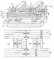
- the array of nonvolatile memory devices 4comprises a three dimensional array of antifuses.
- the array of antifusespreferably comprises a first set of rail stack conductors, a second set of rail stack conductors extending in a different direction than the first set of rail stack conductors, and an insulating layer disposed between the first and the second sets of rail stacks, as illustrated in FIG. 4 .
- the array of FIG. 4Amay have any number of levels of memory cells, such as 2 to 8 levels.
- Each levelincludes a first plurality of parallel spaced-apart rail-stacks running in a first direction and a second plurality of rail-stacks or conductors running in a second direction.
- the first rail-stacksrun perpendicular to the second conductors/rail-stacks and hence form a right angle at their intersections.
- a bitcan be stored at each of the intersections of rail-stacks. However, there are no physically discrete individual memory cells at the intersections, rather memory cells are defined by the rail-stacks and intermediate layers. This makes it easier to fabricate the memory array.
- the term “memory cell”is intended broadly to encompass physically discrete elements or elements that are defined by rail-stacks and intermediate layers, or any other localized region where a bit can be stored. When the array is fabricated all the bits are in the zero (or one) state and after programming, the programmed bits are in the one (or zero) state.
- FIG. 4Aseveral rail-stacks are illustrated in the partial cross-section of the array.
- a rail-stack 16is shown at one height and a half rail-stack 18 is shown at a second height above the first height.
- half rail-stacksare disposed between rail-stack 16 and a substrate 10 .
- the substrate 10may comprise an SOI substrate of the first embodiment or a compound semiconductor substrate of the second embodiment.
- the at least one driver circuit 2is fabricated in substrate 10 under the memory array 4 using, for instance, ordinary MOS and CMOS fabrication techniques. Vias are used to connect conductors within the rail-stacks to the substrate to allow access to each rail-stack in order to program data into the array and to read data from the array. For instance, the circuitry within the substrate 10 may select the rail-stack 16 and the rail stack 18 to program or to read a bit associated with the intersection of these rail-stacks. Alternatively, the at least one driver circuit 2 may be formed within or above the memory array, if desired.
- an insulating layer 12is formed over the substrate 10 containing the driver circuit(s) in order that the array may be fabricated above the substrate.
- This layermay be planarized with, for instance, chemical-mechanical polishing (CMP) to provide a flat surface upon which the array may be fabricated.
- CMPchemical-mechanical polishing
- a conductive layer 14is formed over the substrate.
- conductive layersare used within the rail-stacks and these layers and the resultant conductors may be fabricated from elemental metals such as tungsten, tantalum, aluminum, copper or metal alloys such as MoW.
- Metal silicidesmay also be used such as TiSi 2 , CoSi 2 or a conductive compound such as TiN, WC may be used.
- a highly doped semiconductor layer such as siliconis also suitable. Multiple layer structures may be used selecting one or more of the above.
- a layer of semiconductor material 15such as silicon is formed over the conductive layer.
- Thisis typically a polysilicon layer; however, an amorphous layer may be used.
- Other semiconductor materialsmay be used such as Ge, GaAs, etc.
- this semiconductor layeris highly doped and, as will be seen, forms one-half a diode.
- half rail-stacksare formed. These rail-stacks are “half” or partial rail-stacks since they are approximately half the thickness of the rail-stacks used in the next level.
- the layer 20is a dielectric such as silicon dioxide which is deposited by chemical vapor deposition (CVD) in a blanket deposition over the half rail-stacks and filling the space between the rail-stacks to form a dielectric fill.
- the fill insulating materialsuch as silicon oxide
- the fill materialis then planarized to expose the top surface of the semiconductor layer 15 in the rail stacks, and the antifuse layer 20 , such as silicon oxide, is deposited over the rail stacks and the fill material.
- the layer 20is selectively grown on the upper surface of the silicon layer 15 and only exists on the rail-stacks.
- a full set of memory array rail-stacksis formed on the layer 20 .
- Thiscomprises first the deposition of a lightly doped silicon layer 21 doped with a conductivity-type dopant opposite to that used for the silicon layer 15 , a heavily doped silicon layer 22 doped also opposite to the layer 15 , a conductive layer 23 and a heavily doped silicon layer 24 doped with the same conductivity-type dopant as layers 21 and 22 .
- the rail-stacks shown in FIG. 4Asuch as rail-stack 16 , are formed. These rail-stacks are oriented, as illustrated, in a direction perpendicular to the rail-stacks above and below them.
- the spaces between the rail-stacksare filled with a dielectric such as silicon dioxide.
- a dielectricsuch as silicon dioxide.
- CMPchemical mechanical polishing
- SOGspin-on-glass
- Other fill and planarization methodscan be used.
- another antifuse layer 26is formed, for instance from a dielectric such as silicon dioxide, silicon nitride, silicon oxynitride, amorphous carbon or other insulating materials or combinations of materials. Also an updoped layer of silicon may be used for the antifuse layer.
- a dielectricsuch as silicon dioxide, silicon nitride, silicon oxynitride, amorphous carbon or other insulating materials or combinations of materials.
- an updoped layer of siliconmay be used for the antifuse layer.
- This half rail-stackcomprises a silicon layer 28 doped with a conductivity-type dopant opposite to that of layer 24 . This is a lightly doped layer.
- Another silicon layer 30is formed on layer 28 and this layer is doped with the same conductivity-type dopant as layer 28 ; however, it is more heavily doped. Then a conductive layer 31 is formed above the layer 30 .
- Half rail-stacksare used at the very upper-most level of the array and at the very lowest level of the array. In between the half rail-stacks, full rail-stacks, such as rail-stack 16 , are used throughout the array.
- the silicon layers disposed on the conductive layersextend the entire length of the rail-stacks in the embodiment of FIG. 4 A and are uninterrupted, except possibly where vias are used to provide a conductive path to the substrate 10 .
- FIG. 4Aa path 32 is illustrated from a lower conductor in level 17 to an upper conductor in this level found in the rail-stack 18 .
- This pathis accessed in one embodiment through decoding circuitry in the substrate for both programming and reading of data into and from the array for one bit.
- a relatively high voltagee.g. 5-20V
- This relatively high voltagecauses a breach in the layer 26 creating a diode. Without this high voltage, the layer 26 remains an insulator.
- diodescan be selectively formed so as to program the array. While programming the array with the layers adjacent to the antifuse material being forward-biased is currently preferred, it is also possible to program using a reverse-biasing potential.
- a voltage lower than the programming voltageis used. This lower voltage is applied so as to forward-bias the diode of the cell being accessed and thus allow a sense amplifier to determine whether or not the layer 26 is intact between the rail-stacks. Note that “sneak” or parasitic paths in the array which would interfere with the sensing will include a reverse-biased diode.
- the anode and cathode of the diodesare reversed at each of the successive antifuse layers. This facilitates programming and sensing, since all of the conductors at each level are either bitlines or wordlines. And, for instance, conductors at one height will serve as bitlines for two levels and conductors at the next height serve as wordlines for two levels. This simplifies the decoding and sensing and more importantly reduces processing.
- FIG. 4Billustrates an array of a preferred aspect of the third embodiment where, if the antifuse layer is breached, all the diodes will have a P+/N ⁇ junction. Thus, there will be no diodes with a P ⁇ /N+ junction.
- the first rail-stack 120comprises a first P+ semiconductor (i.e., silicon) layer 125 , a conductor 126 , a second P+ layer 127 and an antifuse layer 128 .
- the thickness of layers 125 - 127may be 400 to 3000 ⁇ , such as 1,000/500/1,000 ⁇ , for layers 125 , 126 and 127 respectively.
- the antifuse layer 128may be about 20-40 ⁇ , preferably about 30 ⁇ thick.
- the second rail-stack 121comprises a first N ⁇ semiconductor (i.e., silicon) layer 129 , a first N+ semiconductor layer 130 , a conductor 131 , a second N+ layer 132 and a second N ⁇ layer 133 .
- the thickness of layers 129 - 133may be 400 to 3000 ⁇ , such as 2,000/500/500/500/2000 ⁇ for layers 129 , 130 , 131 , 132 and 133 respectively.
- the third rail-stack 122contains the same layers as the first rail-stack 120 in reverse order.
- the third rail stackincludes a first P+ semiconductor (i.e., silicon) layer 139 , a conductor 140 , a second P+ layer 142 and an antifuse layer 143 .
- the semiconductor layersmay comprise polysilicon or amorphous silicon.
- the conductorsmay be heavily doped polysilicon, metal, silicide or combinations thereof.
- a CMP planarized dielectric fill 144such as silicon dioxide, is provided in the spaces between the rail-stacks.
- the diodes between the conductors 126 and 131are all P+/N ⁇ type.
- the diodes in the next level between the conductors 131 and 140are again all P+/N ⁇ type.
- the rail-stacks shownare used throughout the memory array so that the entire array has only P+/N ⁇ type diodes in its memory cells.
- the diodes in the illustrated rail-stacks of FIG. 4Bare forward biased towards the conductor 131 and the conductor 141 .
- the diodescan be oriented identically, that is, with all their anodes (or cathodes) pointing upwardly. This can be obtained for the P+/N ⁇ type diodes by having both a P+ doped and N ⁇ doped semiconductor layer in each of the rail-stacks. For instance, layers 132 and 133 would be replaced with a P+ layer and layer 142 would be replaced with N ⁇ and N+ layers. This still maintains only one type of diode (P+/N ⁇ ) throughout the array.
- FIG. 4Bshows that after the antifuse layer is breached, only P+/N ⁇ diodes will be created
- an array with only P ⁇ /N+ type diodescan be fabricated by replacing the P+ layers with N+ layers and replacing the N+ and N ⁇ layers with P+ and P ⁇ layers, respectively.
- the arraycan have the anodes (or cathodes) vertically aligned as discussed above for the P+/N ⁇ type diodes.
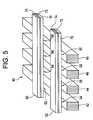
- the array of non-volatile memory devicescomprises a three dimensional array of rail stack EEPROMs. These EEPROMs are three terminal devices in contrast to the two terminal antifuse devices of the third embodiment.
- the arraycomprises a first plurality of spaced-apart conductors disposed at a first height above the substrate in a first direction.
- the arrayalso comprises a second plurality of spaced-apart rail-stacks disposed above the first height in a second direction different from the first direction, each rail-stack including a semiconductor film of a first conductivity type in contact with said first plurality of spaced-apart conductors, a local charge storage film disposed above the semiconductor film and a conductive film disposed above the local charge storage film.
- FIG. 5illustrates a three dimensional array of rail stack EEPROMs according to the fourth preferred embodiment of the present invention.
- the array 40includes a first plurality of spaced-apart conductors such as n+ doped polysilicon bit lines 42 , 44 , 46 , 48 disposed in a first direction above the substrate (not shown).
- a second plurality of spaced-apart “rail stacks” 50 , 52are disposed in a second direction different from the first direction (and preferably orthogonally) at a second height above the substrate so that they are above bit lines 42 , 44 , 46 and 48 and in contact therewith at intersection points 54 , 56 , 58 , 60 , 62 , 64 , 66 , 68 .
- Each rail stack 50 , 52 in this embodimentincludes at least a layer of p ⁇ doped polysilicon 70 .
- a charge storage medium 72such as a dielectric isolated floating gate, an ONO dielectric film (i.e., a SiO 2 /Si 3 N 4-x O 1.5x /SiO 2 film, where 0 ⁇ x ⁇ 1) or an insulating layer containing conductive nanocrystals.
- a conductive wordline 74which may comprise n+ doped polysilicon is disposed over the charge storage medium 72 .
- a planarized oxide material(not shown) may be deposited in the spaces between adjacent bit lines and rail stacks. A conventional chemical mechanical polishing (CMP) process may be used to accomplish this.
- the bit lines 42 , 44 , 46 , 48may comprise p+ doped rather than n+ doped polysilicon, while layer 70 may comprise n ⁇ doped rather than p ⁇ doped polysilicon.
- the memory array structure of FIG. 5can be easily extrapolated to three dimensions. To do this, an interlayer insulating layer is placed over the rail stacks 50 , 52 after the CMP process. This layer prevents shorting one set of wordlines with the next set of bit lines. Then another layer of bit lines 42 , 44 , 46 , 48 is constructed over the interlayer insulating layer followed by an oxide deposition and a CMP step, followed by a deposition of another set of rail stacks. This process can be repeated a number of times, as desired, to form two or more device levels (such as eight levels, for example).
- the array of non-volatile memory devices 4comprises a three dimensional array of two terminal pillar memory devices.
- one device of the three-dimensional memoryis illustrated.
- the deviceincludes a conductor 81 at one level and a conductor 80 at the next level in the array.
- a pillar structureis formed in alignment with the conductors 80 and 81 .
- This pillar structureforms a cell in accordance with the present embodiment.
- the cellincludes a steering element and a storage stack.
- the steering elementcomprises a junction diode which contains a p+ region 82 and an n ⁇ region 10 .
- the storage stackcomprises a tunnel oxide region 84 , a charge trapping region 86 and a blocking oxide 85 .
- the charge trapping region 86may comprise silicon nitride, silicon oxynitride, an ONO dielectric film or silicon nanocrystals in an insulating layer.
- the conductors 80 and 81are shared with cells disposed above and below the single cell shown in FIG. 6 .
- FIG. 7shows another preferred aspect of this embodiment where again there are spaced-apart, parallel conductors at one level, such as conductor 91 , and parallel, spaced-apart conductors at the next level, such as conductor 90 .
- a pillar structureis again fabricated between the conductors 90 and 91 .
- the storage stackcomprising the blocking oxide 93 , charge trapping region 94 and tunnel oxide 95 is disposed between the p and n regions of the diode. Specifically, the p+ region 92 of the diode is in contact with the blocking oxide 93 and the n ⁇ region 96 is in contact with the tunnel oxide 95 .
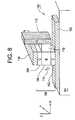
- the array of non-volatile memory devices 4comprises a three dimensional array of three terminal pillar memory devices, such as pillar EEPROMs. These devices differ from the devices of the previous embodiment in that they contain three rather than two terminals.
- a three terminal nonvolatile stackable pillar memory device 100is illustrated in FIG. 8 .
- Pillar memory device 100includes a first contact region 102 formed on a first input/output (I/O) 103 conductor (i.e., electrode), which is formed above a plane (x-y) of a substrate 101 .
- a semiconductor body 104is formed directly on the first contact region 102 and a second contact region 106 is formed directly on the body 104 .
- the contact regions 102 and 104are heavily doped semiconductor regions of a first conductivity type (i.e., source and drain regions), while the body is a lightly doped semiconductor region of a second conductivity type (i.e., a channel).
- the semiconductor regions 102 , 104 and 106preferably comprise doped polysilicon.
- a second I/O conductor 116i.e., electrode is formed on the second contact region 106 .
- the first contact region 102 , the body 104 , and the second contact region 106are each vertically aligned with one another to form a pillar 108 .
- a control gate 112is formed adjacent to and in direct contact with the charge storage medium or region 110 .
- the control gate 112 and charge storage medium 110are constructed so that they lie laterally adjacent to pillar 108 so that they may electrically communicate with the pillar 108 .
- the charge storage mediumis the region that electrically screens the control gate and the channel region addressed by the control gate.
- the charge storage mediummay comprise a silicon oxide/nitride/oxide (“ONO”) dielectric film, conductive nanocrystals in an insulating layer or a floating gate located between a tunnel dielectric layer and a control gate dielectric layer.
- ONOsilicon oxide/nitride/oxide
- the pillar memory cell of the present embodimentcan be easily stacked in a three dimensional array with source/drain conductors 103 and 116 running parallel or perpendicular to each other and parallel to the plane of the substrate 101 without requiring the use of vertical interconnect strategies for the source and drain connections.
- the conductor 112 to the control gatemay be run vertically (as shown in FIG. 8 ) or horizontally.
- memory device 100 shown in FIG. 8includes a charge storage medium 110 and a control gate 112 formed on only one side or surface of pillar 108
- the pillar memory device of the present embodimentcan be fabricated so that the entire body of the pillar 108 is surrounded by a single charge storage member 110 and a single control gate 112 .
- each surface of the pillar 108can have an independently controlled charge storage member and control gate and thereby enable multiple bits of data to be stored in a single pillar memory device.
- the use of multiple charge storage members and control gatesenables the storage of multiple values on a single pillar device by determining how much of the channel is exposed to charge.
- each face of body 104 of pillar 108can have different doping densities to create different threshold voltages for each face to further enable the pillar memory to store additional states and therefore additional bits.
- the array of non-volatile memory devices 4comprises a three dimensional array of thin film transistor (“TFT”) EEPROMs.
- This arraycomprises a plurality of vertically separated device levels, each level comprising an array of TFT EEPROMs.
- Each TFT EEPROMincludes a channel, source and drain regions, a control gate, and a charge storage region between the channel and the control gate.
- the arrayalso comprises a plurality of bit line columns in each device level, each bit line contacting the source or the drain regions of the TFT EEPROMs.
- the arrayfurther comprises a plurality of word line rows in each device level, and at least one interlayer insulating layer located between the device levels.
- FIG. 9illustrates a preferred three dimensional memory array 200 according to the seventh preferred embodiment of the present invention.
- the three dimensional memory array 200is a three dimensional array of TFT EEPROMs.
- Each TFT EEPROMcontains source and drain regions 217 , a channel 219 , a control gate 243 , control gate sidewall spacers (not shown for clarity in FIG. 9 ) and a charge storage region 207 between the channel and the control gate.
- the channel 219 of each TFT EEPROMcomprises amorphous silicon or polysilicon.
- the charge storage region 207may comprise a silicon oxide/nitride/oxide (“ONO”) dielectric film, isolated nanocrystals or a floating gate located between a tunneling dielectric and a control gate dielectric layer.
- ONOsilicon oxide/nitride/oxide
- the memory array 200also contains a plurality of bit line columns 225 .
- Each bit line 225contacts the source or the drain regions 217 of a plurality of TFT EEPROMs.
- the columns of the bit lines 225extend substantially perpendicular to the source-channel-drain direction of the TFT EEPROMs (i.e., a small deviation from the perpendicular direction is included in the term “substantially perpendicular”).
- the bit lines 225 in each device levelare shaped as rails which extend under the intergate insulating layer 227 .
- the bit linesinclude the buried diffusion regions formed during the source and drain 217 doping steps and the overlying silicide 223 layers.
- the source and drain regions 217are formed in the bit lines 225 where the word lines 241 intersect (i.e., overly) the bit lines 225 .
- the doped source and drain regions 217are located adjacent to the TFT EEPROM channel regions 219 .
- the memory array 200also includes a plurality of word line rows 241 .
- Each word line 241contacts the control gates 243 of a plurality of TFT EEPROMs 200 .
- the word linescan themselves comprise the control gates.
- the rows of word linesextend substantially parallel to the source-channel-drain direction of the TFT EEPROMs.
- the plurality of word lines 241are self aligned to the control gates 243 of the array of TFT EEPROMs or the word lines themselves comprise the control gates. If floating gates, but not control gates are included in the array, then the word lines are self aligned to the floating gates and to the control gate dielectric.
- the word linesare also self aligned to the channel and the charge storage regions of the TFT EEPROMs located below the respective word lines.
- Each device level 245 of the arrayis separated and decoupled in the vertical direction by an interlayer insulating layer 203 .
- the interlayer insulating layer 203also isolates adjacent word lines 241 and adjacent portions of the channels 219 below the respective word lines 241 in each device level 245 .
- Each level of the TFT EEPROMsmay be formed by forming a plurality of gate electrodes 209 on the active silicon areas.
- the source and drain regions 217are implanted into the active silicon areas using the gates 209 as a mask.
- the remaining silicon active areasform the TFT channel regions 219 .
- Sidewall spacers(not shown) are formed on the gates 209 .
- silicide regions 223are formed on the source and drain regions 217 by the salicide method.
- the intergate insulating layer 227is deposited over the gates 209 and planarized to expose the gates 209 .
- a sacrificial blocking layermay also be formed over the gates 209 .
- the blocking layeris removed after layer 227 is planarized to expose the gates 209 .
- a conductive materialis deposited and patterned to form the word lines 241 and control gates 243 .
- the channels 219 and the charge storage region 207are also patterned during the same etching step using the same photores
- the memory devices of the preferred embodiments of the present inventionmay be arranged in a three dimensional virtual ground array (VGA) nonvolatile flash memory.
- VGAvirtual ground array
- the devicesmay also be formed in nonvolatile flash memory architectures other than VGA, such as NOR-type memory and Dual String NOR (DuSNOR) memory architectures.
- each EEPROMoccurs by hot carrier injection.
- hot carrier injectiona voltage is placed across a diode (i.e., between a source and a drain of a TFT EEPROM).
- the hot carriersi.e., hot electrons and holes
- This procedureis a relatively high power event.
- FN tunnelingFor low power portable applications where both program/erase and read power are important, a flash nonvolatile memory using Fowler-Nordheim tunneling (“FN tunneling”) for both program and erase may be used.
- FN tunnelingresults from applying a voltage across a dielectric.
- a voltageis applied between a control gate and a source and/or a drain region of the TFT, for writing and erasing the TFT EEPROM. This is in contrast with hot carrier injection programming, where a voltage is applied between the source and the drain regions.
- a flash memory array which uses FN tunneling for program and eraseis advantageous because thousands of bits in such a flash memory array may be programmed at the same time. Also, FN tunneling is a very efficient way of programming since most (close to 100%) of the current goes to program the device. This is in contrast with hot carrier injection where only about 1-2% of the source-drain current goes to program the device.
- charge storage devicessuch as TFT EEPROMs
- TFT EEPROMsare arranged in a flash memory array configuration which utilizes FN tunneling programming.
- the TFT EEPROMsmay be arranged in the rail stack, pillar or self-aligned TFT or configurations of the previous embodiments.
- the TFT EEPROMsare arranged in the rail stack configuration.
- the VGAis not compatible with FN tunneling since the whole channel polysilicon inverts along the length of the pulsed-high word line and will then program cells in addition to the one that needs programming. Therefore, the FN tunneling rail stack (crosspoint) flash array differs from the VGA in that in the FN tunneling array the active polysilicon layer is patterned into polysilicon islands to allow FN tunneling programming.
- an extra photolithographic masking stepis added to the process of making the rail stack array shown in FIG. 5 during which the polysilicon active layer is etched into islands in each device cell.
- the same photoresist maskcan be used to define (i.e., etch) the charge storage regions in each cell.
- the flash memory array 330is preferably formed over a planarized interlayer insulating layer 331 , such as a CMP planarized silicon oxide layer.
- Layer 331is formed over a substrate (not shown) as in the previous embodiments.
- Each device of the array(shown by dashed lines 332 in FIG. 10A ) is thus a TFT because it is formed over an insulating layer.
- the array 330contains a first plurality of spaced-apart conductive bit lines 333 disposed at a first height above the substrate in a first direction.
- the arrayalso contains a second plurality of spaced-apart rail-stacks 335 .
- the rail stacksare disposed at a second height in a second direction different from the first direction.
- the bit lines 333 and the rail stacks 335are arranged perpendicular to each other.
- the TFT EEPROM 332is formed at the intersection of the rail stacks 335 and the bit lines 333 .
- Each rail-stack 335includes a plurality of semiconductor islands 337 , which comprise the active regions of the TFT EEPROMs 332 .
- One surface of the islands 337is in contact with the bit lines 333 .
- Each rail stack 335also includes a conductive word line 339 and a charge storage region 341 disposed between a second surface of the semiconductor islands 337 and the word line 339 .
- the semiconductor islands 337preferably comprise polysilicon of a first conductivity type (i.e., P ⁇ or N ⁇ ). However, the islands may comprise amorphous silicon if desired.
- the polysilicon islands 337include source and drain regions 343 of a second conductivity type (i.e., N+ or P+). The source and drain regions 343 are located at contacting intersections between the bit line conductors 333 and the rail stacks 335 .
- the bit lines 333preferably comprise polysilicon of the second conductivity type (i.e., N+ or P+).
- the bit lines 333contact the source and drain regions 343 .
- the source and drain regionsare formed by outdiffusion of dopants from the bit lines.
- an optional metal or a metal silicide layer(not shown in FIG. 10A ) may be disposed in contact with the bit lines 333 to increase the conductivity of the bit lines.
- the space between said spaced-apart bit line conductors 333is filled with a planarized insulating filler material 345 , such as silicon oxide.
- the charge storage regions 341may comprise a dielectric isolated floating gate, electrically isolated nanocrystals or an ONO dielectric stack, as in the previous embodiments.
- An exemplary array having a dielectric isolated floating gateis illustrated in FIGS. 10 A and B.
- the charge storage region 341comprises a polysilicon floating gate 347 between a tunnel dielectric 349 , such as a silicon oxide layer, and a control gate dielectric 351 (also known as the intergate or interpoly dielectric) made of a material such as silicon oxide or an ONO layer stack.
- the lateral sides 353 of the tunnel dielectric 349 and the floating gate 347are aligned to the lateral sides 355 of the semiconductor islands 337 .
- the control gate dielectric 351extends between the semiconductor islands 337 and contacts the planarized insulating material 345 between the semiconductor islands 337 .
- the floating gate 347may be made from hemispherical grain polysilicon which has a textured surface to maximize the control gate to floating gate coupling. Alternatively, the coupling may be increased by increasing the floating gate height, by forming horns or protrusions in the floating gate, or by roughening the floating gate surface.
- the word line 339comprises a polysilicon layer of a second conductivity type (i.e., N+ or P+) and a metal or a metal silicide layer in contact with the polysilicon layer.
- the word line 339acts as a control gate of the TFT EEPROM in locations where it overlies the charge storage regions 341 . Thus, formation of a separate control gate for each TFT is not required.
- the rail stacks 335are disposed above the bit lines 333 , as shown in FIGS. 10A and B . However, if desired, the rail stacks 335 may be disposed below the bit lines 333 in each device level, (i.e., bottom gate TFT EEPROMs are formed).
- the word line 339 , the charge storage regions 341 and the semiconductor islands 337are aligned in a plane 356 perpendicular to the substrate and parallel to a source to drain direction.
- the rail stacks 335are separated by a second planarized insulating layer 357 , such as silicon oxide.
- the flash memory arraymay comprise a two dimensional array
- the flash memory arraycomprises a monolithic three dimensional array comprising a plurality of device levels.
- three device levelsare shown in FIG. 10 A.
- the device levelsare separated by an interlayer insulating layer 359 , such as a silicon oxide layer.
- layers 357 and 359may comprise the same silicon oxide layer which is deposited above and between the rail stacks 359 , and then planarized by CMP.
- either its drain bit line or its source bit line 333are grounded while the positive programming voltage is applied to the selected word line 339 adjacent to the device 332 (which is a high impedance node). All other word lines on the same device level are grounded while all other bit lines on the same level device can float or are placed at a slight positive voltage. This means that only the selected cell 332 experiences the programming voltage across it.
- the floating gate 347is pulled high while the source and/or drain 343 are grounded. Electrons tunnel to the floating gate 347 from the source and/or drain 343 and an inversion channel is formed in the silicon channel 337 .
- the current to program such a cell to get a threshold voltage shift of about 5V in approximately one millisecondis several picoamps.
- bit lines 333can be grounded and a negative voltage pulse is applied to the selected word line 339 .
- All other word linescan either be grounded or can float. All other bit lines float or are placed at a slight negative voltage.
- a plurality (or all) of EEPROM cells in the arraycan be erased at the same time by pulsing a plurality of word lines to a high negative value while all bit lines are grounded.
- the selected wordlineis grounded while the selected cell's bit lines are pulsed positive. All other word lines float or are pulsed slightly positive while all the other bitlines are grounded.
- the driver circuit(s) 2may comprise conventional CMOS thin film transistors formed in an SOI substrate or bulk CMOS transistors formed in a compound semiconductor substrate.
- FIG. 11illustrates a CMOS TFT array according to a ninth preferred embodiment of the present invention that may be used in a driver circuit 2 .
- the NMOS and PMOS transistors of the CMOS arraymay be formed adjacent to each other in the same device level in an alternating fashion (i.e., as alternating NMOS and PMOS transistors).
- the one charge carrier type transistorsi.e., NMOS or PMOS
- the other charge carrier type transistorsi.e., PMOS or NMOS
- a common gate linealso known as a word line in memory devices
- the driver circuit 2 of the ninth preferred embodimentcomprises a plurality of vertically stacked, common gate CMOS TFT transistors.
- FIG. 11One device level of a vertically stacked, common gate CMOS array in a rail stack configuration according to the ninth preferred embodiment of the present invention is shown in FIG. 11 .
- the arraymay also be arranged in a pillar or self-aligned TFT configurations illustrated in FIGS. 8 and 9 .
- the CMOS array in FIG. 11is similar to the array illustrated in FIG. 5 , except that transistors of different charge carrier type are formed on either side of the gate line.
- the NMOS transistorsare arranged below the PMOS transistors. However, it should be understood that the PMOS transistors may be arranged below the NMOS transistors if desired.
- the array of CMOS devices 400is preferably formed over a planarized interlayer insulating layer 401 , such as a CMP planarized silicon oxide layer.
- Layer 401is formed over a substrate (not shown) as in the previous embodiments.
- Each CMOS deviceis thus a CMOS TFT because it is formed over an insulating layer.
- the arrayincludes a plurality of gate lines (i.e., word lines) 403 (only one gate line is shown in the cross sectional view of FIG. 11 ).
- the gate linecomprises a first N+ polysilicon layer 405 , a silicide layer 407 , such as a TiSi x or WSi x layer, over the first polysilicon layer and a second P+ polysilicon layer 409 above the silicide layer.
- the gate line 403acts as a gate electrode in each TFT. Thus, no separate gate electrodes connected to the gate lines are required.
- a first insulating layer 411is disposed adjacent to a first side of the gate electrode 403 .
- This insulating layer 411may be a conventional gate dielectric.
- the insulating layer 411is a charge storage layer (i.e., charge trapping media), such as an ONO stack or isolated nanocrystals, to form charge storage CMOS TFTS, such as EEPROM CMOS TFTs. If floating gate type EEPROM CMOS TFTs are desired, then a floating gate and a control gate dielectric may be added between the insulating layer 411 and the gate line 403 .
- a p-type semiconductor layer 413such as a P ⁇ polysilicon layer, is disposed on a side of the first insulating layer opposite to the gate 403 .
- This layercontains the NMOS TFT bodies.
- N+ source and drain regions 415are disposed in layer 413 .
- the portions of layer 413 between regions 415comprise NMOS TFT channel regions.
- the source and drain regions 415are formed by outdiffusion of n-type dopants from the source and drain electrodes (i.e., bit lines) 417 .
- regions 415may be formed by any other method, such as by masking and ion implantation.
- the electrodes 417contact the source and drain regions 415 and are disposed on the bottom of the p-type semiconductor layer 413 (i.e., on the side of layer 413 opposite to the first insulating layer 411 ).
- the electrodes 417comprise N+ polysilicon rails which extend in a direction perpendicular to the gate line 403 .
- an optional metal or metal silicide layeris formed in contact with electrodes 417 to increase their conductivity.
- the electrodes 417may comprise metal or metal silicide instead of the heavily doped polysilicon, if desired.
- a planar insulating filler layer 418such as silicon oxide, is disposed between the source and drain electrodes 417 .
- each NMOS TFT 419is located between adjacent source and drain regions 415 and comprises a portion of layers 405 , 411 , 413 and 417 , as illustrated in FIG. 11 .
- the PMOS TFTS 421are located above the NMOS TFTs 419 .
- the PMOS TFTs 421include a second insulating layer 423 adjacent to a second side of the gate electrode 403 .
- layer 423is located on the P+ polysilicon layer 409 of the gate line 403 .
- the insulating layer 423may be a conventional gate dielectric.
- the insulating layer 423is a charge storage layer (i.e., charge trapping media), such as an ONO stack or isolated nanocrystals, to form charge storage CMOS TFTS, such as EEPROM CMOS TFTs. If floating gate type EEPROM CMOS TFTs are desired, then a floating gate and a control gate dielectric may be added between the insulating layer 423 and the gate line 403 .
- An n-type semiconductor layer 425such as an N ⁇ polysilicon layer, is disposed above the second insulating layer 423 .
- Layer 425is disposed on the opposite side of layer 423 from the gate electrode 403 .
- P+ source and drain regions 427are disposed in layer 425 , such that regions of layer 425 between the source and drain regions 427 comprise channel regions of PMOS TFTs.
- Source and drain electrodes 429are disposed over the N ⁇ polysilicon layer 425 and in contact with the source and drain regions 429 . Thus, the electrodes 429 are disposed on top side of the N ⁇ polysilicon layer 425 opposite to the second insulating layer 423 .
- a planar insulating filler layer 431such as silicon oxide, is disposed between the source and drain electrodes 429 . If desired, an optional metal or metal silicide layer is formed in contact with electrodes 429 to increase their conductivity.
- each PMOS TFT 421is located between adjacent source and drain regions 427 and comprises a portion of layers 409 , 423 , 425 and 429 , as illustrated in FIG. 11.
- a TFT EEPROM CMOS device( 419 and 421 ) is formed at each intersection of the first and the third spaced-apart electrodes or conductors 417 , 429 and the common gate line 403 .
- the CMOS structuremay be inverted and the PMOS TFTs formed below NMOS TFTs. It should be noted that NMOS and PMOS electrodes (i.e., bit lines) do not have to fall directly on top of each other, although they preferably should have the same pitch.
- NMOS and PMOS transistorsthus can have different channel lengths, but the pitch (and thus array size) will be limited by the longer of the two channel lengths.
- TFTs of one conductivity typei.e., NMOS or PMOS TFTs
- TFTs of the other conductivity typei.e., PMOS or NMOS
- the CMOS of this aspectcomprises one EEPROM TFT and one non-EEPROM TFT.
- the TFT CMOS device array 400 illustrated in FIG. 11is highly planar and compact.
- the NMOS source and drain electrodes 417comprise polysilicon rails which extend above the interlayer insulating layer 401 in a first plane parallel to the substrate surface.
- the p-type polysilicon layer 413extends above the source and drain electrodes 417 in a second plane.
- the gate line 403extends above layers 417 , 413 and 411 in a third plane.
- the n-type polysilicon layer 425extends above the gate line 403 in a fourth plane.
- the PMOS source and drain electrodes 429comprise polysilicon rails which extend above the n-type semiconductor layer 425 in a fifth plane. Each of the five planes does not intersect any of the other planes.
- the TFT CMOS array 400is also self aligned.
- the gate electrode 403 , the first insulating layer 411 , the p-type semiconductor layer 413 , the second insulating layer 423 and the n-type semiconductor layer 425comprise a rail stack which is located in a plane parallel to the substrate.
- the rail stackextends perpendicular to the source and drain electrodes 417 , 429 .
- the gate electrode 403 , the first insulating layer 411 , the p-type semiconductor layer 413 , the second insulating layer 423 and the n-type semiconductor layer 425are self aligned in a plane perpendicular to the substrate and parallel to the source to drain direction.
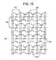
- the resulting TFT CMOS arrayis a matrix of NMOS 419 and PMOS 421 devices with common gates 403 .
- the array shown in FIG. 12is an unprogrammed or unconfigured array.
- the arraycan then be configured into logic elements or memory devices by rupturing the gate dielectric (i.e., the charge storage film or region) to form a conductive link which connects the gate lines (i.e., word line rows) 403 and source and drain electrodes 417 , 429 (i.e., bit lines), or by storing charge in the charge storage regions of either NMOS or PMOS transistors to raise their threshold voltages and keep them permanently off.
- the array of TFT CMOS EEPROM devices 400may be used to form either logic elements or a memory array.
- the same semiconductor device in the unconfigured arraymay be used either as an antifuse or as an EPROM or an EEPROM.
- a driver circuitcomprising a plurality of charge storage devices and a plurality of antifuse devices.
- the circuitmay comprise a field programmable gate array or a programmable logic device.
- the plurality of charge storage devices and the plurality of antifuse devicescomprise a same set of devices. This greatly simplifies the fabrication of the circuit. These devices function as charge storage devices when a first programming voltage is applied to the devices to turn these devices off by increasing their threshold voltage. These devices also function as antifuses when a second programming voltage higher than a first voltage is applied to the devices.
- the second voltagemay be any voltage which is sufficient to form a conductive link through the charge storage region.
- the firsti.e., charge storage voltage
- the second voltage sufficient to form the conductive linkmay be 5-50 volts, depending on the device characteristics.
- charge storage and antifuse semiconductor deviceshaving a different structure may be provided.
- any charge storage devices which function as an antifuse when a conductive link has been formed through its charge storage regionare within the scope of the ninth preferred embodiment.
- any deviceis within the scope of the ninth preferred embodiment if the device contains a semiconductor active region, a charge storage region adjacent to the semiconductor active region, a first electrode and second electrodes, and where charge is stored in the charge storage region when a first programming voltage is applied between the first and the second electrodes, and a conductive link is formed through the charge storage region to form a conductive path between the first and the second electrodes. Therefore, a charge storage device which is capable of being used as an antifuse is not limited to rail stack TFT EEPROMs. Such charge storage devices may include the pillar or self aligned TFT EEPROMs and diodes with charge storage regions of the previous embodiments.
- FIG. 13illustrates how a 4 ⁇ 4 cell array of the circuit of FIG. 12 can be programmed into an inverter 443 .
- a high voltageis applied between gate (i.e., word) line 445 and bit lines 447 , which will be used to carry the output voltage, V out .
- Thiscauses conductive antifuse links 448 to form to electrically connect lines 445 and 447 .
- a programming voltageis applied to all other transistors 450 to increase their threshold voltage to turn them off, except to NMOS transistors 455 and PMOS transistors 457 .
- the NMOS 455 and PMOS 457 transistorsform the inverter.
- V inWhen a high voltage, V in , is provided into gate line 449 , then a low voltage, V out , is read out, and vice-versa.
- Voltages V SS (i.e., ground) and V DD (i.e., power supply voltage)are provided into bit lines 451 and 453 which are connected to transistors 455 and 457 .
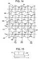
- FIG. 14illustrates how a 4 ⁇ 4 cell array of the circuit of FIG. 12 can be programmed into a two input NAND gate 460 .
- a high voltageis applied between gate (i.e., word) line 445 and bit lines 447 , which will be used to carry the output voltage, V out .
- Thiscauses conductive antifuse links 448 to form to electrically connect lines 445 and 447 .
- a programming voltageis provided to all other transistors 450 to increase their threshold voltage to turn them off, except for PMOS transistors 461 and 465 and NMOS transistors 463 and 465 .
- the transistors 461 , 463 , 465 and 467form the NAND gate.
- Input voltages V in1 and V in2are provided into gate lines 469 and 471 .
- CMOS 461 / 463is connected to gate line 469
- transistors 465 and 467are connected to gate line 471 .
- Voltages V SS and V DDare provided into bit lines 473 and 475 .
- NMOS 467is connected to bit line 475
- PMOS 461 and 465are connected to bit line 473 .
- Output voltagescan be read out from lines 445 or 447 , which are connected by a blown antifuse 448 .
- the driver circuits in an SOI or a compound semiconductor substrateBy forming the driver circuits in an SOI or a compound semiconductor substrate, numerous advantages may be realized. For example, by forming the driver circuits in SOI substrates, the leakage current between the devices of the driver circuits is improved compared to the devices formed in a monocrystalline silicon substrate. Furthermore, the radiation hardness of the devices formed in an SOI substrate is improved compared to the radiation hardness of the devices formed in a monocrystalline silicon substrate.
- the driver circuits formed in a silicon carbide substrateBy forming the driver circuits in a silicon carbide substrate, the leakage current and radiation hardness of the driver circuits is improved compared to the driver circuits formed in a silicon substrate. Furthermore, the driver circuits formed in a silicon carbide substrate can withstand a higher operating voltage than the driver circuits formed in a silicon substrates. Thus, the memory array of the preferred embodiments may be used in an environment where it will be subjected to high radiation doses, such as in military devices and in space craft, by forming the driver circuits in an SOI or a silicon carbide substrate.
- the operating speed of the driver circuitsis higher than the operating speed of the driver circuits formed in a silicon substrate.
- the memory array of the preferred embodimentsmay be used in an environment where high device operating speed is required.
- driver circuits in SOI or compound semiconductor substratesmay be monolithically integrated (i.e., formed over the same substrate) with additional devices which are ordinarily formed on SOI or compound semiconductor substrates.
- the driver circuit(s) 2 , the memory array 4 and the additional device(s) 500are monolithically formed on the same substrate, which contains an insulating surface 3 .
- the additional device 500is formed over the same substrate as the driver circuits 2 by depositing a semiconductor layer over the substrate and forming the device 500 in the deposited semiconductor layer.
- the additional device 500which is ordinarily formed on SOI or compound semiconductor substrate is a non-memory device, such as an optoelectronic component.
- An optoelectronic componentmay comprise a laser, an light emitting diode (LED) or a semiconductor photodetector. These devices are ordinarily formed on a III-V semiconductor, glass, plastic or ceramic substrates.
- the driver circuit 2is also formed on a III-V, glass, plastic or ceramic substrate.
- the additional device 500which is ordinarily formed on a compound semiconductor substrate is a microwave circuit (such as a monolithic microwave integrated circuit or MMIC) or a radio frequency circuit.
- the driver circuit 2is also formed in a III-V substrate.
- the additional device 500which is ordinarily formed on an SOI substrate, such as a glass, plastic or ceramic substrate, is a liquid crystal display (“LCD”). Since an LCD usually has TFT driver circuits and TFTs in the display matrix, it is preferable to form the driver circuits 2 of the memory array during the same step as the LCD driver circuits, and to form the TFT EEPROMs of one level of the seventh embodiment during the same step as the matrix TFTs of LCD.
- LCDliquid crystal display
- the additional device 500which is ordinarily formed on an SOI substrate, such as a flexible plastic substrate is a smart card processing circuit.
- the memory array and the smart card chipmay be formed on the same plastic substrate for use as a smart card.
- a metal silicide layerwas formed in contact with a silicon layer, such as a polysilicon word line or bit line.
- a silicon layersuch as a polysilicon word line or bit line.
- One preferred method of forming a titanium silicide layer in contact with a silicon layeris by using a silicon cap and a TiN layer.
- the titanium silicide layeris formed on an undoped amorphous silicon cap layer.
- the cap layeris formed on a heavily doped silicon layer, such as a polysilicon or amorphous silicon layer doped to a concentration in excess of 10 19 cm ⁇ 3 , such as 10 19 cm ⁇ 3 to 10 21 cm ⁇ .
- the cap layeris preferably deposited on P+ polysilicon or N+ amorphous silicon layers. The N+ amorphous silicon may then be recrystallized into N+ polysilicon during subsequent annealing steps.
- a method of forming a titanium silicide (TiSi 2 ) layercomprises the following steps.
- a heavily doped polysilicon layeris deposited.
- a P+ polysilicon layeris boron doped to a concentration of 5 ⁇ 10 20 cm ⁇ 3 , and has a thickness of about 1400 Angstroms.
- a cap layer of undoped amorphous siliconis deposited on the P+ polysilicon layer. The cap may be 600 Angstroms thick, for example.
- a titanium layeris deposited on the cap. The titanium layer may be 250 Angstroms thick, for example.
- a titanium nitride layeris deposited on the titanium layer. The titanium nitride layer may be 100 Angstroms thick, for example. Other layer thicknesses may be used, as required.
- the layersare annealed at a temperature below 650° C. for less than five minutes to react the titanium and the silicon in the cap to form a C49 phase TiSi 2 layer.
- the annealmay be carried out at 600° C. for 1 minute, for example.
- another P+ polysilicon layeris deposited over the stack and the stack is etched into a thin “wire” or “rail”, such as a word line or bit line.
- the wire or railmay be 0.25 mm wide or less.
- the titanium silicideis then transformed from the C49 to the C54 phase by a high temperature (i.e., above 650° C.) anneal.
- the annealcan take place before or after the wires or rails are patterned, at 800° C.
- each Si/Ti/TiN film stackfor one minute, for example.
- dopant diffusion and thermal grooving of the TiSi 2is minimized.
- Multiple film stackscan be deposited and etched sequentially.
Landscapes
- Semiconductor Memories (AREA)
Abstract
Description
Claims (20)
Priority Applications (2)
| Application Number | Priority Date | Filing Date | Title |
|---|---|---|---|
| US09/927,642US6888750B2 (en) | 2000-04-28 | 2001-08-13 | Nonvolatile memory on SOI and compound semiconductor substrates and method of fabrication |
| PCT/US2002/021318WO2003017285A1 (en) | 2001-08-13 | 2002-08-12 | Nonvolatile memory on soi and compound semiconductor substrates and methods of fabrication |
Applications Claiming Priority (3)
| Application Number | Priority Date | Filing Date | Title |
|---|---|---|---|
| US56062600A | 2000-04-28 | 2000-04-28 | |
| US09/814,727US6420215B1 (en) | 2000-04-28 | 2001-03-21 | Three-dimensional memory array and method of fabrication |
| US09/927,642US6888750B2 (en) | 2000-04-28 | 2001-08-13 | Nonvolatile memory on SOI and compound semiconductor substrates and method of fabrication |
Related Parent Applications (1)
| Application Number | Title | Priority Date | Filing Date |
|---|---|---|---|
| US09/814,727Continuation-In-PartUS6420215B1 (en) | 2000-04-28 | 2001-03-21 | Three-dimensional memory array and method of fabrication |
Publications (2)
| Publication Number | Publication Date |
|---|---|
| US20010055838A1 US20010055838A1 (en) | 2001-12-27 |
| US6888750B2true US6888750B2 (en) | 2005-05-03 |
Family
ID=25455036
Family Applications (1)
| Application Number | Title | Priority Date | Filing Date |
|---|---|---|---|
| US09/927,642Expired - LifetimeUS6888750B2 (en) | 2000-04-28 | 2001-08-13 | Nonvolatile memory on SOI and compound semiconductor substrates and method of fabrication |
Country Status (2)
| Country | Link |
|---|---|
| US (1) | US6888750B2 (en) |
| WO (1) | WO2003017285A1 (en) |
Cited By (218)
| Publication number | Priority date | Publication date | Assignee | Title |
|---|---|---|---|---|
| US20030040157A1 (en)* | 2001-08-24 | 2003-02-27 | Leonard Forbes | Vertical transistor with horizontal gate layers |
| US20040023441A1 (en)* | 2002-08-01 | 2004-02-05 | Trivedi Jigish D. | Edge intensive antifuse and method for making the same |
| US20040070421A1 (en)* | 2002-10-15 | 2004-04-15 | Kapoor Ashok K. | Programmable logic devices with silicon-germanium circuitry and associated methods |
| US20040145399A1 (en)* | 2002-10-03 | 2004-07-29 | Arup Bhattacharyya | High performance three-dimensional TFT-based CMOS inverters, and computer systems utilizing such novel CMOS inverters |
| US20040207001A1 (en)* | 2001-03-28 | 2004-10-21 | Matrix Semiconductor, Inc. | Two mask floating gate EEPROM and method of making |
| US20040206996A1 (en)* | 2000-08-14 | 2004-10-21 | Matrix Semiconductor, Inc. | Dense arrays and charge storage devices |
| US20040212395A1 (en)* | 2002-07-08 | 2004-10-28 | Madurawe Raminda Udaya | Three dimensional integrated circuits |
| US20040245577A1 (en)* | 2003-06-03 | 2004-12-09 | Arup Bhattacharyya | SRAM devices, and electronic systems comprising SRAM devices |
| US20050078514A1 (en)* | 2003-09-30 | 2005-04-14 | Scheuerlein Roy E. | Multiple twin cell non-volatile memory array and logic block structure and method therefor |
| US20050093022A1 (en)* | 2002-08-09 | 2005-05-05 | Macronix International Co., Ltd. | Spacer chalcogenide memory device |
| US20050112804A1 (en)* | 2002-03-13 | 2005-05-26 | Matrix Semiconductor, Inc. | Silicide-silicon oxide-semiconductor antifuse device and method of making |
| US20050180248A1 (en)* | 2003-03-31 | 2005-08-18 | Scheuerlein Roy E. | Word line arrangement having multi-layer word line segments for three-dimensional memory array |
| US20060038212A1 (en)* | 2004-08-19 | 2006-02-23 | John Moore | Structure for amorphous carbon based non-volatile memory |
| US20060110878A1 (en)* | 2004-11-22 | 2006-05-25 | Macronix International Co., Ltd. | Side wall active pin memory and manufacturing method |
| US20060145181A1 (en)* | 2004-12-30 | 2006-07-06 | Klaus Ufert | Opto-electronic memory element on the basis of organic metalloporphyrin molecules |
| US20060157679A1 (en)* | 2005-01-19 | 2006-07-20 | Matrix Semiconductor, Inc. | Structure and method for biasing phase change memory array for reliable writing |
| US20060202251A1 (en)* | 2005-02-25 | 2006-09-14 | Micron Technology, Inc. | Scalable high performance non-volatile memory cells using multi-mechanism carrier transport |
| US20060249735A1 (en)* | 2001-08-13 | 2006-11-09 | Sandisk Corporation | TFT mask ROM and method for making same |
| US20060284158A1 (en)* | 2005-06-17 | 2006-12-21 | Macronix International Co., Ltd. | Self-aligned, embedded phase change ram and manufacturing method |
| US20060284214A1 (en)* | 2005-06-17 | 2006-12-21 | Macronix International Co., Ltd. | Thin film fuse phase change cell with thermal isolation layer and manufacturing method |
| US20060286743A1 (en)* | 2005-06-17 | 2006-12-21 | Macronix International Co., Ltd. | Method for Manufacturing a Narrow Structure on an Integrated Circuit |
| US20070080448A1 (en)* | 2005-10-11 | 2007-04-12 | International Business Machines Corporation | Method and structure for optimizing yield of 3-d chip manufacture |
| US20070081410A1 (en)* | 2005-10-07 | 2007-04-12 | International Business Machines Corporation | Wafer level i/o test and repair enabled by i/o layer |
| US20070108429A1 (en)* | 2005-11-14 | 2007-05-17 | Macronix International Co., Ltd. | Pipe shaped phase change memory |
| US20070109843A1 (en)* | 2005-11-15 | 2007-05-17 | Macronix International Co., Ltd. | Phase Change Memory Device and Manufacturing Method |
| US20070108430A1 (en)* | 2005-11-15 | 2007-05-17 | Macronix International Co., Ltd. | Thermally contained/insulated phase change memory device and method (combined) |
| US20070117315A1 (en)* | 2005-11-22 | 2007-05-24 | Macronix International Co., Ltd. | Memory cell device and manufacturing method |
| US20070121363A1 (en)* | 2005-11-28 | 2007-05-31 | Macronix International Co., Ltd. | Phase Change Memory Cell and Manufacturing Method |
| US20070126040A1 (en)* | 2005-11-21 | 2007-06-07 | Hsiang-Lan Lung | Vacuum cell thermal isolation for a phase change memory device |
| US20070131922A1 (en)* | 2005-12-13 | 2007-06-14 | Macronix International Co., Ltd. | Thin Film Fuse Phase Change Cell with Thermal Isolation Pad and Manufacturing Method |
| US20070131980A1 (en)* | 2005-11-21 | 2007-06-14 | Lung Hsiang L | Vacuum jacket for phase change memory element |
| US20070134876A1 (en)* | 2005-12-09 | 2007-06-14 | Macronix International Co., Ltd. | Stacked thin film transistor, non-volatile memory devices and methods for fabricating the same |
| US20070131999A1 (en)* | 2005-12-09 | 2007-06-14 | Macronix International Co., Ltd. | Gated Diode Nonvolatile Memory Process |
| US20070145575A1 (en)* | 2004-01-27 | 2007-06-28 | Masato Mori | Circuit board and method for mounting chip component |
| US20070155172A1 (en)* | 2005-12-05 | 2007-07-05 | Macronix International Co., Ltd. | Manufacturing Method for Phase Change RAM with Electrode Layer Process |
| US20070161186A1 (en)* | 2006-01-09 | 2007-07-12 | Macronix International Co., Ltd. | Programmable Resistive RAM and Manufacturing Method |
| US20070158690A1 (en)* | 2006-01-09 | 2007-07-12 | Macronix International Co., Ltd. | Programmable Resistive RAM and Manufacturing Method |
| US20070158645A1 (en)* | 2006-01-11 | 2007-07-12 | Macronix International Co., Ltd. | Self-align planerized bottom electrode phase change memory and manufacturing method |
| US20070158862A1 (en)* | 2005-11-21 | 2007-07-12 | Hsiang-Lan Lung | Vacuum jacketed electrode for phase change memory element |
| US20070158632A1 (en)* | 2006-01-09 | 2007-07-12 | Macronix International Co., Ltd. | Method for Fabricating a Pillar-Shaped Phase Change Memory Element |
| US20070158633A1 (en)* | 2005-12-27 | 2007-07-12 | Macronix International Co., Ltd. | Method for Forming Self-Aligned Thermal Isolation Cell for a Variable Resistance Memory Array |
| US20070173019A1 (en)* | 2006-01-09 | 2007-07-26 | Macronix International Co., Ltd. | Programmable Resistive Ram and Manufacturing Method |
| US20070173063A1 (en)* | 2006-01-24 | 2007-07-26 | Macronix International Co., Ltd. | Self-aligned manufacturing method, and manufacturing method for thin film fuse phase change ram |
| US20070176261A1 (en)* | 2006-01-30 | 2007-08-02 | Macronix International Co., Ltd. | Vertical Side Wall Active Pin Structures in a Phase Change Memory and Manufacturing Methods |
| US20070241371A1 (en)* | 2006-04-17 | 2007-10-18 | Macronix International Co., Ltd. | Memory device and manufacturing method |
| US20070242511A1 (en)* | 2002-12-31 | 2007-10-18 | En-Hsing Chen | Nand memory array incorporating capacitance boosting of channel regions in unselected memory cells and method for operation of same |
| US20070257300A1 (en)* | 2006-05-05 | 2007-11-08 | Macronix International Co., Ltd. | Structures and Methods of a Bistable Resistive Random Access Memory |
| US20070258291A1 (en)* | 2006-05-08 | 2007-11-08 | Macronix International Co., Ltd. | Methods and apparatus for implementing bit-by-bit erase of a flash memory device |
| US20070262388A1 (en)* | 2006-05-09 | 2007-11-15 | Macronix International Co., Ltd. | Bridge Resistance Random Access Memory Device and Method With A Singular Contact Structure |
| US20070263423A1 (en)* | 2003-03-31 | 2007-11-15 | Scheuerlein Roy E | Three-dimensional memory device incorporating segmented array line memory array |
| US20070274121A1 (en)* | 2005-06-17 | 2007-11-29 | Macronix International Co., Ltd. | Multi-level memory cell having phase change element and asymmetrical thermal boundary |
| US20070278529A1 (en)* | 2006-05-30 | 2007-12-06 | Macronix International Co., Ltd. | Resistor random access memory cell with l-shaped electrode |
| US20070281420A1 (en)* | 2006-05-30 | 2007-12-06 | Macronix International Co., Ltd. | Resistor random access memory cell with reduced active area and reduced contact areas |
| US20080014676A1 (en)* | 2006-07-12 | 2008-01-17 | Macronix International Co., Ltd. | Method for Making a Pillar-Type Phase Change Memory Element |
| US20080043520A1 (en)* | 2006-02-07 | 2008-02-21 | Chen Shih H | I-shaped phase change memory cell with thermal isolation |
| US20080061341A1 (en)* | 2006-09-11 | 2008-03-13 | Macronix International Co., Ltd. | Memory Device Having Wide Area Phase Change Element and Small Electrode Contact Area |
| US20080087942A1 (en)* | 2006-10-11 | 2008-04-17 | Macronix International Co., Ltd. | Vertical channel memory and manufacturing method thereof and operating method using the same |
| US20080087946A1 (en)* | 2006-10-11 | 2008-04-17 | Macronix International Co., Ltd. | Vertical channel transistor structure and manufacturing method thereof |
| US20080096341A1 (en)* | 2006-10-24 | 2008-04-24 | Macronix International Co., Ltd. | Method for Manufacturing a Resistor Random Access Memory with Reduced Active Area and Reduced Contact Areas |
| US20080096375A1 (en)* | 2006-10-18 | 2008-04-24 | Macronix International Co., Ltd. | Method for Making Memory Cell Device |
| US20080094885A1 (en)* | 2006-10-24 | 2008-04-24 | Macronix International Co., Ltd. | Bistable Resistance Random Access Memory Structures with Multiple Memory Layers and Multilevel Memory States |
| US20080101149A1 (en)* | 2004-12-30 | 2008-05-01 | Fasoli Luca G | Hierarchical decoding of dense memory arrays using multiple levels of multiple-headed decoders |
| US20080099791A1 (en)* | 2006-10-04 | 2008-05-01 | Macronix International Co., Ltd. | Memory Cell Device with Circumferentially-Extending Memory Element |
| US20080106923A1 (en)* | 2006-10-24 | 2008-05-08 | Macronix International Co., Ltd. | Phase Change Memory Cells with Dual Access Devices |
| US20080109993A1 (en)* | 2006-11-10 | 2008-05-15 | Ji Man Myeong | Hinge module for an electronic device and electronic device having the same |
| US20080116440A1 (en)* | 2006-11-16 | 2008-05-22 | Macronix International Co., Ltd. | Resistance Random Access Memory Structure for Enhanced Retention |
| US20080121861A1 (en)* | 2006-08-16 | 2008-05-29 | Macronix International Co., Ltd. | Self-Aligned Structure and Method for Confining a Melting Point in a Resistor Random Access Memory |
| US20080138931A1 (en)* | 2006-12-06 | 2008-06-12 | Macronix International Co., Ltd. | Method for Making a Self-Converged Void and Bottom Electrode for Memoery Cell |
| US20080137400A1 (en)* | 2006-12-06 | 2008-06-12 | Macronix International Co., Ltd. | Phase Change Memory Cell with Thermal Barrier and Method for Fabricating the Same |
| US20080135824A1 (en)* | 2006-12-07 | 2008-06-12 | Macronix International Co., Ltd. | Method and Structure of a Multi-Level Cell Resistance Random Access Memory with Metal Oxides |
| US20080138929A1 (en)* | 2006-12-06 | 2008-06-12 | Macronix International Co., Ltd. | Method for Making a Self-Converged Memory Material Element for Memory Cell |
| US20080135920A1 (en)* | 2005-12-09 | 2008-06-12 | Macronix International Co., Ltd. | Gated Diode Nonvolatile Memory Process |
| US7388771B2 (en) | 2006-10-24 | 2008-06-17 | Macronix International Co., Ltd. | Methods of operating a bistable resistance random access memory with multiple memory layers and multilevel memory states |
| US20080142984A1 (en)* | 2006-12-15 | 2008-06-19 | Macronix International Co., Ltd. | Multi-Layer Electrode Structure |
| US20080145951A1 (en)* | 2006-12-19 | 2008-06-19 | Liesl Folks | High density spin torque three dimensional (3D) memory arrays addressed with microwave current |
| US20080144353A1 (en)* | 2006-12-13 | 2008-06-19 | Macronix International Co., Ltd. | Method, Apparatus and Computer Program Product for Read Before Programming Process on Programmable Resistive Memory Cell |
| US20080157053A1 (en)* | 2006-12-28 | 2008-07-03 | Macronix International Co., Ltd. | Resistor Random Access Memory Cell Device |
| US20080165570A1 (en)* | 2007-01-05 | 2008-07-10 | Macronix International Co., Ltd. | Current Compliant Sensing Architecture for Multilevel Phase Change Memory |
| US20080165571A1 (en)* | 2007-01-09 | 2008-07-10 | Macronix International Co., Ltd. | Method, Apparatus and Computer Program Product for Read Before Programming Process on Multiple Programmable Resistive Memory Cell |
| US20080179685A1 (en)* | 2007-01-31 | 2008-07-31 | Petti Christopher J | Embedded memory in a cmos circuit and methods of forming the same |
| US20080182367A1 (en)* | 2007-01-31 | 2008-07-31 | Petti Christopher J | Embedded memory in a cmos circuit and methods of forming the same |
| US20080186761A1 (en)* | 2007-02-07 | 2008-08-07 | Macronix International Co., Ltd. | Memory Cell with Separate Read and Program Paths |
| US20080186755A1 (en)* | 2007-02-05 | 2008-08-07 | Macronix International Co., Ltd. | Memory cell device and programming methods |
| US20080185730A1 (en)* | 2007-02-02 | 2008-08-07 | Macronix International Co., Ltd. | Memory cell device with coplanar electrode surface and method |
| US20080192534A1 (en)* | 2007-02-08 | 2008-08-14 | Macronix International Co., Ltd. | Memory element with reduced-current phase change element |
| US20080191187A1 (en)* | 2007-02-12 | 2008-08-14 | Macronix International Co., Ltd. | Method for manufacturing a phase change memory device with pillar bottom electrode |
| US20080191186A1 (en)* | 2007-02-14 | 2008-08-14 | Macronix International Co., Ltd. | Phase change memory cell with filled sidewall memory element and method for fabricating the same |
| US7414258B2 (en) | 2005-11-16 | 2008-08-19 | Macronix International Co., Ltd. | Spacer electrode small pin phase change memory RAM and manufacturing method |
| US20080197333A1 (en)* | 2007-02-21 | 2008-08-21 | Macronix International Co., Ltd. | Programmable Resistive Memory Cell with Self-Forming Gap |
| US20080197334A1 (en)* | 2007-02-21 | 2008-08-21 | Macronix International Co., Ltd. | Phase Change Memory Cell with Heater and Method for Fabricating the Same |
| US20080203375A1 (en)* | 2007-02-27 | 2008-08-28 | Macronix International Co., Ltd. | Memory Cell with Memory Element Contacting Ring-Shaped Upper End of Bottom Electrode |
| US7423300B2 (en) | 2006-05-24 | 2008-09-09 | Macronix International Co., Ltd. | Single-mask phase change memory element |
| US20080247224A1 (en)* | 2007-04-06 | 2008-10-09 | Macronix International Co., Ltd. | Phase Change Memory Bridge Cell with Diode Isolation Device |
| US7440315B2 (en) | 2007-01-09 | 2008-10-21 | Macronix International Co., Ltd. | Method, apparatus and computer program product for stepped reset programming process on programmable resistive memory cell |
| US20080259672A1 (en)* | 2007-04-17 | 2008-10-23 | Macronix International Co., Ltd. | 4f2 self align side wall active phase change memory |
| US20080266940A1 (en)* | 2005-11-21 | 2008-10-30 | Erh-Kun Lai | Air Cell Thermal Isolation for a Memory Array Formed of a Programmable Resistive Material |
| US20080266933A1 (en)* | 2007-04-24 | 2008-10-30 | Macronix International Co., Ltd. | Method and Apparatus for Refreshing Programmable Resistive Memory |
| US20080273364A1 (en)* | 2007-05-04 | 2008-11-06 | Macronix International Co., Ltd. | Memory structure with embeded multi-type memory |
| US7450411B2 (en) | 2005-11-15 | 2008-11-11 | Macronix International Co., Ltd. | Phase change memory device and manufacturing method |
| US20090003110A1 (en)* | 2007-06-29 | 2009-01-01 | Tyler Thorp | Methods and apparatus for extending the effective thermal operating range of a memory |
| US20090003109A1 (en)* | 2007-06-29 | 2009-01-01 | Tyler Thorp | Methods and apparatus for extending the effective thermal operating range of a memory |
| US20090014706A1 (en)* | 2007-07-13 | 2009-01-15 | Macronix International Co., Ltd. | 4f2 self align fin bottom electrodes fet drive phase change memory |
| US20090034323A1 (en)* | 2007-08-02 | 2009-02-05 | Macronix International Co., Ltd. | Phase change memory with dual word lines and source lines and method of operating same |
| US20090032793A1 (en)* | 2007-08-03 | 2009-02-05 | Macronix International Co., Ltd. | Resistor Random Access Memory Structure Having a Defined Small Area of Electrical Contact |
| US20090032796A1 (en)* | 2007-07-31 | 2009-02-05 | Macronix International Co., Ltd. | Phase change memory bridge cell |
| US20090039414A1 (en)* | 2007-08-09 | 2009-02-12 | Macronix International Co., Ltd. | Charge trapping memory cell with high speed erase |
| US20090072216A1 (en)* | 2007-09-14 | 2009-03-19 | Macronix International Co., Ltd. | Phase change memory cell array with self-converged bottom electrode and method for manufacturing |
| US20090072215A1 (en)* | 2007-09-14 | 2009-03-19 | Macronix International Co., Ltd. | Phase change memory cell in via array with self-aligned, self-converged bottom electrode and method for manufacturing |
| US7507986B2 (en) | 2005-11-21 | 2009-03-24 | Macronix International Co., Ltd. | Thermal isolation for an active-sidewall phase change memory cell |
| US7514334B2 (en) | 2005-06-17 | 2009-04-07 | Macronix International Co., Ltd. | Thin film plate phase change RAM circuit and manufacturing method |
| US20090095948A1 (en)* | 2007-10-12 | 2009-04-16 | Macronix International Co., Ltd. | Programmable Resistive Memory with Diode Structure |
| US7521364B2 (en) | 2005-12-02 | 2009-04-21 | Macronix Internation Co., Ltd. | Surface topology improvement method for plug surface areas |
| US20090122588A1 (en)* | 2007-11-14 | 2009-05-14 | Macronix International Co., Ltd. | Phase change memory cell including a thermal protect bottom electrode and manufacturing methods |
| US7534647B2 (en) | 2005-06-17 | 2009-05-19 | Macronix International Co., Ltd. | Damascene phase change RAM and manufacturing method |
| US7535756B2 (en) | 2007-01-31 | 2009-05-19 | Macronix International Co., Ltd. | Method to tighten set distribution for PCRAM |
| US20090147564A1 (en)* | 2007-12-07 | 2009-06-11 | Macronix International Co., Ltd. | Phase change memory cell having interface structures with essentially equal thermal impedances and manufacturing methods |
| US20090168482A1 (en)* | 2007-12-28 | 2009-07-02 | Samsung Electronics Co., Ltd. | Three-dimensional memory device |
| US20090180324A1 (en)* | 2008-01-15 | 2009-07-16 | Ramaswamy D V Nirmal | Semiconductor Constructions, NAND Unit Cells, Methods Of Forming Semiconductor Constructions, And Methods Of Forming NAND Unit Cells |
| US20090184310A1 (en)* | 2008-01-18 | 2009-07-23 | Macronix International Co., Ltd. | Memory cell with memory element contacting an inverted t-shaped bottom electrode |
| US20090189138A1 (en)* | 2008-01-28 | 2009-07-30 | Macronix International Co., Ltd. | Fill-in etching free pore device |
| US7569844B2 (en) | 2007-04-17 | 2009-08-04 | Macronix International Co., Ltd. | Memory cell sidewall contacting side electrode |
| US7579613B2 (en) | 2005-06-17 | 2009-08-25 | Macronix International Co., Ltd. | Thin film fuse phase change RAM and manufacturing method |
| US20090242880A1 (en)* | 2008-03-25 | 2009-10-01 | Macronix International Co., Ltd. | Thermally stabilized electrode structure |
| US20090251963A1 (en)* | 2008-04-03 | 2009-10-08 | Samsung Electronics Co., Ltd. | Non-volatile memory device and method of manufacturing the same |
| US20090261313A1 (en)* | 2008-04-22 | 2009-10-22 | Macronix International Co., Ltd. | Memory cell having a buried phase change region and method for fabricating the same |
| US20090309087A1 (en)* | 2008-06-12 | 2009-12-17 | Macronix International Co., Ltd. | Phase change memory cell having top and bottom sidewall contacts |
| US7635855B2 (en) | 2005-11-15 | 2009-12-22 | Macronix International Co., Ltd. | I-shaped phase change memory cell |
| US7639527B2 (en) | 2008-01-07 | 2009-12-29 | Macronix International Co., Ltd. | Phase change memory dynamic resistance test and manufacturing methods |
| US20100019215A1 (en)* | 2008-07-22 | 2010-01-28 | Macronix International Co., Ltd. | Mushroom type memory cell having self-aligned bottom electrode and diode access device |
| US20100032732A1 (en)* | 2008-08-06 | 2010-02-11 | International Business Machines Corporation | Electrical antifuse having a multi-thickness dielectric layer |
| US7663135B2 (en) | 2007-01-31 | 2010-02-16 | Macronix International Co., Ltd. | Memory cell having a side electrode contact |
| US20100039867A1 (en)* | 2008-08-15 | 2010-02-18 | Macronix International Co., Ltd. | Electrically Isolated Gated Diode Nonvolatile Memory |
| US20100046285A1 (en)* | 2008-08-19 | 2010-02-25 | Macronix International Co., Ltd. | Multiple phase change materials in an integrated circuit for system on a chip application |
| US20100067301A1 (en)* | 2008-09-17 | 2010-03-18 | Kim Suk-Pil | Columnar non-volatile memory devices with auxiliary transistors and methods of operating the same |
| US20100067285A1 (en)* | 2008-09-12 | 2010-03-18 | Macronix International Co., Ltd. | Novel sensing circuit for pcram applications |
| US7682868B2 (en) | 2006-12-06 | 2010-03-23 | Macronix International Co., Ltd. | Method for making a keyhole opening during the manufacture of a memory cell |
| US7688619B2 (en) | 2005-11-28 | 2010-03-30 | Macronix International Co., Ltd. | Phase change memory cell and manufacturing method |
| US7696506B2 (en) | 2006-06-27 | 2010-04-13 | Macronix International Co., Ltd. | Memory cell with memory material insulation and manufacturing method |
| US20100091558A1 (en)* | 2008-10-10 | 2010-04-15 | Macronix International Co., Ltd. | Dielectric-Sandwiched Pillar Memory Device |
| US7701750B2 (en) | 2008-05-08 | 2010-04-20 | Macronix International Co., Ltd. | Phase change device having two or more substantial amorphous regions in high resistance state |
| US20100117048A1 (en)* | 2008-11-07 | 2010-05-13 | Macronix International Co., Ltd. | Memory cell access device having a pn-junction with polycrystalline and single-crystal semiconductor regions |
| US20100171188A1 (en)* | 2009-01-07 | 2010-07-08 | Macronix International Co., Ltd. | Integrated circuit device with single crystal silicon on silicide and manufacturing method |
| US20100184259A1 (en)* | 2007-06-27 | 2010-07-22 | Radigan Steven J | Method for fabricating a 3-d integrated circuit using a hard mask of silicon-oxynitride on amorphous carbon |
| US7777215B2 (en) | 2007-07-20 | 2010-08-17 | Macronix International Co., Ltd. | Resistive memory structure with buffer layer |
| US7781807B2 (en) | 2006-11-30 | 2010-08-24 | Kabushiki Kaisha Toshiba | Non-volatile semiconductor storage device |
| US7786461B2 (en) | 2007-04-03 | 2010-08-31 | Macronix International Co., Ltd. | Memory structure with reduced-size memory element between memory material portions |
| US7825398B2 (en) | 2008-04-07 | 2010-11-02 | Macronix International Co., Ltd. | Memory cell having improved mechanical stability |
| US7869270B2 (en) | 2008-12-29 | 2011-01-11 | Macronix International Co., Ltd. | Set algorithm for phase change memory cell |
| US7894254B2 (en) | 2009-07-15 | 2011-02-22 | Macronix International Co., Ltd. | Refresh circuitry for phase change memory |
| US7910907B2 (en) | 2006-03-15 | 2011-03-22 | Macronix International Co., Ltd. | Manufacturing method for pipe-shaped electrode phase change memory |
| CN101369582B (en)* | 2007-08-15 | 2011-03-30 | 旺宏电子股份有限公司 | Vertical non-volatile memory and manufacturing method thereof |
| US7919766B2 (en) | 2007-10-22 | 2011-04-05 | Macronix International Co., Ltd. | Method for making self aligning pillar memory cell device |
| US7928421B2 (en) | 2006-04-21 | 2011-04-19 | Macronix International Co., Ltd. | Phase change memory cell with vacuum spacer |
| US7932506B2 (en) | 2008-07-22 | 2011-04-26 | Macronix International Co., Ltd. | Fully self-aligned pore-type memory cell having diode access device |
| US7933139B2 (en) | 2009-05-15 | 2011-04-26 | Macronix International Co., Ltd. | One-transistor, one-resistor, one-capacitor phase change memory |
| US7968876B2 (en) | 2009-05-22 | 2011-06-28 | Macronix International Co., Ltd. | Phase change memory cell having vertical channel access transistor |
| US20110169064A1 (en)* | 2010-01-11 | 2011-07-14 | International Business Machines Corporation | Read transistor for single poly non-volatile memory using body contacted soi device |
| US8030635B2 (en) | 2009-01-13 | 2011-10-04 | Macronix International Co., Ltd. | Polysilicon plug bipolar transistor for phase change memory |
| US8030634B2 (en) | 2008-03-31 | 2011-10-04 | Macronix International Co., Ltd. | Memory array with diode driver and method for fabricating the same |
| US20110241126A1 (en)* | 2008-12-22 | 2011-10-06 | Cambridge Silicon Radio Ltd. | Rf cmos transistor design |
| US8036014B2 (en)* | 2008-11-06 | 2011-10-11 | Macronix International Co., Ltd. | Phase change memory program method without over-reset |
| US8064247B2 (en) | 2009-01-14 | 2011-11-22 | Macronix International Co., Ltd. | Rewritable memory device based on segregation/re-absorption |
| US8062833B2 (en) | 2005-12-30 | 2011-11-22 | Macronix International Co., Ltd. | Chalcogenide layer etching method |
| US8064248B2 (en) | 2009-09-17 | 2011-11-22 | Macronix International Co., Ltd. | 2T2R-1T1R mix mode phase change memory array |
| US8077505B2 (en) | 2008-05-07 | 2011-12-13 | Macronix International Co., Ltd. | Bipolar switching of phase change device |
| US8084760B2 (en) | 2009-04-20 | 2011-12-27 | Macronix International Co., Ltd. | Ring-shaped electrode and manufacturing method for same |
| US8089137B2 (en) | 2009-01-07 | 2012-01-03 | Macronix International Co., Ltd. | Integrated circuit memory with single crystal silicon on silicide driver and manufacturing method |
| US8097871B2 (en) | 2009-04-30 | 2012-01-17 | Macronix International Co., Ltd. | Low operational current phase change memory structures |
| US8107283B2 (en) | 2009-01-12 | 2012-01-31 | Macronix International Co., Ltd. | Method for setting PCRAM devices |
| US8110822B2 (en) | 2009-07-15 | 2012-02-07 | Macronix International Co., Ltd. | Thermal protect PCRAM structure and methods for making |
| US8134857B2 (en) | 2008-06-27 | 2012-03-13 | Macronix International Co., Ltd. | Methods for high speed reading operation of phase change memory and device employing same |
| US8158965B2 (en) | 2008-02-05 | 2012-04-17 | Macronix International Co., Ltd. | Heating center PCRAM structure and methods for making |
| US8173987B2 (en) | 2009-04-27 | 2012-05-08 | Macronix International Co., Ltd. | Integrated circuit 3D phase change memory array and manufacturing method |
| US8178387B2 (en) | 2009-10-23 | 2012-05-15 | Macronix International Co., Ltd. | Methods for reducing recrystallization time for a phase change material |
| US8198619B2 (en) | 2009-07-15 | 2012-06-12 | Macronix International Co., Ltd. | Phase change memory cell structure |
| US8238149B2 (en) | 2009-06-25 | 2012-08-07 | Macronix International Co., Ltd. | Methods and apparatus for reducing defect bits in phase change memory |
| US20120224408A1 (en)* | 2011-03-03 | 2012-09-06 | Tianhong Yan | Three dimensional memory system with column pipeline |
| US8310864B2 (en) | 2010-06-15 | 2012-11-13 | Macronix International Co., Ltd. | Self-aligned bit line under word line memory array |
| US8324681B2 (en) | 2005-12-09 | 2012-12-04 | Macronix International Co., Ltd. | Stacked non-volatile memory device and methods for fabricating the same |
| US8324605B2 (en) | 2008-10-02 | 2012-12-04 | Macronix International Co., Ltd. | Dielectric mesh isolated phase change structure for phase change memory |
| US8350316B2 (en) | 2009-05-22 | 2013-01-08 | Macronix International Co., Ltd. | Phase change memory cells having vertical channel access transistor and memory plane |
| US8363463B2 (en) | 2009-06-25 | 2013-01-29 | Macronix International Co., Ltd. | Phase change memory having one or more non-constant doping profiles |
| US8395935B2 (en) | 2010-10-06 | 2013-03-12 | Macronix International Co., Ltd. | Cross-point self-aligned reduced cell size phase change memory |
| US8406033B2 (en) | 2009-06-22 | 2013-03-26 | Macronix International Co., Ltd. | Memory device and method for sensing and fixing margin cells |
| US8467238B2 (en) | 2010-11-15 | 2013-06-18 | Macronix International Co., Ltd. | Dynamic pulse operation for phase change memory |
| US8497705B2 (en) | 2010-11-09 | 2013-07-30 | Macronix International Co., Ltd. | Phase change device for interconnection of programmable logic device |
| US8553476B2 (en) | 2011-03-03 | 2013-10-08 | Sandisk 3D Llc | Three dimensional memory system with page of data across word lines |
| US8605495B2 (en) | 2011-05-09 | 2013-12-10 | Macronix International Co., Ltd. | Isolation device free memory |
| US8643162B2 (en) | 2007-11-19 | 2014-02-04 | Raminda Udaya Madurawe | Pads and pin-outs in three dimensional integrated circuits |
| US8664689B2 (en) | 2008-11-07 | 2014-03-04 | Macronix International Co., Ltd. | Memory cell access device having a pn-junction with polycrystalline plug and single-crystal semiconductor regions |
| US8709890B2 (en) | 2011-12-12 | 2014-04-29 | International Business Machines Corporation | Method and structure for forming ETSOI capacitors, diodes, resistors and back gate contacts |
| US8729521B2 (en) | 2010-05-12 | 2014-05-20 | Macronix International Co., Ltd. | Self aligned fin-type programmable memory cell |
| US8748258B2 (en) | 2011-12-12 | 2014-06-10 | International Business Machines Corporation | Method and structure for forming on-chip high quality capacitors with ETSOI transistors |
| US8809829B2 (en) | 2009-06-15 | 2014-08-19 | Macronix International Co., Ltd. | Phase change memory having stabilized microstructure and manufacturing method |
| US8861271B1 (en) | 2012-03-16 | 2014-10-14 | Cypress Semiconductor Corporation | High reliability non-volatile static random access memory devices, methods and systems |
| US8933536B2 (en) | 2009-01-22 | 2015-01-13 | Macronix International Co., Ltd. | Polysilicon pillar bipolar transistor with self-aligned memory element |
| US8987700B2 (en) | 2011-12-02 | 2015-03-24 | Macronix International Co., Ltd. | Thermally confined electrode for programmable resistance memory |
| US9053766B2 (en) | 2011-03-03 | 2015-06-09 | Sandisk 3D, Llc | Three dimensional memory system with intelligent select circuit |
| US9087169B2 (en) | 2008-09-14 | 2015-07-21 | Raminda U. Madurawe | Automated metal pattern generation for integrated circuits |
| US20150249188A1 (en)* | 2013-05-30 | 2015-09-03 | International Business Machines Corporation | Heterojunction light emitting diode |
| US9159412B1 (en) | 2014-07-15 | 2015-10-13 | Macronix International Co., Ltd. | Staggered write and verify for phase change memory |
| US9240405B2 (en) | 2011-04-19 | 2016-01-19 | Macronix International Co., Ltd. | Memory with off-chip controller |
| US9336879B2 (en) | 2014-01-24 | 2016-05-10 | Macronix International Co., Ltd. | Multiple phase change materials in an integrated circuit for system on a chip application |
| US9355740B2 (en) | 2014-03-12 | 2016-05-31 | Kabushiki Kaisha Toshiba | Semiconductor nonvolatile memory device with one-time programmable memories |
| US9397665B2 (en) | 2003-12-04 | 2016-07-19 | Callahan Cellular L.L.C. | Programmable structured arrays |
| US9478495B1 (en) | 2015-10-26 | 2016-10-25 | Sandisk Technologies Llc | Three dimensional memory device containing aluminum source contact via structure and method of making thereof |
| US9547736B2 (en) | 2002-07-08 | 2017-01-17 | Callahan Cellular L.L.C. | Timing exact design conversions from FPGA to ASIC |
| US9559113B2 (en) | 2014-05-01 | 2017-01-31 | Macronix International Co., Ltd. | SSL/GSL gate oxide in 3D vertical channel NAND |
| US9627395B2 (en) | 2015-02-11 | 2017-04-18 | Sandisk Technologies Llc | Enhanced channel mobility three-dimensional memory structure and method of making thereof |
| US9672906B2 (en) | 2015-06-19 | 2017-06-06 | Macronix International Co., Ltd. | Phase change memory with inter-granular switching |
| US9806088B2 (en)* | 2016-02-15 | 2017-10-31 | Toshiba Memory Corporation | Semiconductor memory device having memory cells arranged three-dimensionally and method of manufacturing the same |
| USRE47311E1 (en) | 2005-01-03 | 2019-03-19 | Macronix International Co., Ltd. | Silicon on insulator and thin film transistor bandgap engineered split gate memory |
| US20190252318A1 (en)* | 2016-01-29 | 2019-08-15 | Taiwan Semiconductor Manufacturing Company, Ltd. | Semiconductor Device and Method |
| US10559578B2 (en)* | 2017-06-02 | 2020-02-11 | Applied Materials, Inc. | Deposition of cobalt films with high deposition rate |
| US10665581B1 (en) | 2019-01-23 | 2020-05-26 | Sandisk Technologies Llc | Three-dimensional semiconductor chip containing memory die bonded to both sides of a support die and methods of making the same |
| US10879260B2 (en) | 2019-02-28 | 2020-12-29 | Sandisk Technologies Llc | Bonded assembly of a support die and plural memory dies containing laterally shifted vertical interconnections and methods for making the same |
| US12094904B2 (en) | 2020-10-06 | 2024-09-17 | Samsung Electronics Co., Ltd. | Image sensor |
| TWI872091B (en)* | 2019-12-30 | 2025-02-11 | 南韓商愛思開海力士有限公司 | Memory device and method for fabricating the same |
Families Citing this family (99)
| Publication number | Priority date | Publication date | Assignee | Title |
|---|---|---|---|---|
| US6888750B2 (en) | 2000-04-28 | 2005-05-03 | Matrix Semiconductor, Inc. | Nonvolatile memory on SOI and compound semiconductor substrates and method of fabrication |
| US7087975B2 (en)* | 2000-12-28 | 2006-08-08 | Infineon Technologies Ag | Area efficient stacking of antifuses in semiconductor device |
| US6593624B2 (en) | 2001-09-25 | 2003-07-15 | Matrix Semiconductor, Inc. | Thin film transistors with vertically offset drain regions |
| US7068544B2 (en)* | 2001-08-30 | 2006-06-27 | Micron Technology, Inc. | Flash memory with low tunnel barrier interpoly insulators |
| US7087954B2 (en) | 2001-08-30 | 2006-08-08 | Micron Technology, Inc. | In service programmable logic arrays with low tunnel barrier interpoly insulators |
| US7476925B2 (en) | 2001-08-30 | 2009-01-13 | Micron Technology, Inc. | Atomic layer deposition of metal oxide and/or low asymmetrical tunnel barrier interploy insulators |
| US7135734B2 (en)* | 2001-08-30 | 2006-11-14 | Micron Technology, Inc. | Graded composition metal oxide tunnel barrier interpoly insulators |
| US6754108B2 (en) | 2001-08-30 | 2004-06-22 | Micron Technology, Inc. | DRAM cells with repressed floating gate memory, low tunnel barrier interpoly insulators |
| US7132711B2 (en) | 2001-08-30 | 2006-11-07 | Micron Technology, Inc. | Programmable array logic or memory with p-channel devices and asymmetrical tunnel barriers |
| US7075829B2 (en) | 2001-08-30 | 2006-07-11 | Micron Technology, Inc. | Programmable memory address and decode circuits with low tunnel barrier interpoly insulators |
| US6815781B2 (en)* | 2001-09-25 | 2004-11-09 | Matrix Semiconductor, Inc. | Inverted staggered thin film transistor with salicided source/drain structures and method of making same |
| US6897522B2 (en) | 2001-10-31 | 2005-05-24 | Sandisk Corporation | Multi-state non-volatile integrated circuit memory systems that employ dielectric storage elements |
| US6925007B2 (en) | 2001-10-31 | 2005-08-02 | Sandisk Corporation | Multi-state non-volatile integrated circuit memory systems that employ dielectric storage elements |
| US6534841B1 (en)* | 2001-12-14 | 2003-03-18 | Hewlett-Packard Company | Continuous antifuse material in memory structure |
| US6703652B2 (en)* | 2002-01-16 | 2004-03-09 | Hewlett-Packard Development Company, L.P. | Memory structure and method making |
| US6885573B2 (en)* | 2002-03-15 | 2005-04-26 | Hewlett-Packard Development Company, L.P. | Diode for use in MRAM devices and method of manufacture |
| US6579760B1 (en)* | 2002-03-28 | 2003-06-17 | Macronix International Co., Ltd. | Self-aligned, programmable phase change memory |
| US6940085B2 (en) | 2002-04-02 | 2005-09-06 | Hewlett-Packard Development Company, I.P. | Memory structures |
| US6643159B2 (en) | 2002-04-02 | 2003-11-04 | Hewlett-Packard Development Company, L.P. | Cubic memory array |
| US6661691B2 (en) | 2002-04-02 | 2003-12-09 | Hewlett-Packard Development Company, L.P. | Interconnection structure and methods |
| US6821848B2 (en)* | 2002-04-02 | 2004-11-23 | Hewlett-Packard Development Company, L.P. | Tunnel-junction structures and methods |
| US20030183868A1 (en)* | 2002-04-02 | 2003-10-02 | Peter Fricke | Memory structures |
| US6967350B2 (en)* | 2002-04-02 | 2005-11-22 | Hewlett-Packard Development Company, L.P. | Memory structures |
| US6737675B2 (en) | 2002-06-27 | 2004-05-18 | Matrix Semiconductor, Inc. | High density 3D rail stack arrays |
| US6774458B2 (en) | 2002-07-23 | 2004-08-10 | Hewlett Packard Development Company, L.P. | Vertical interconnection structure and methods |
| US6710409B1 (en) | 2002-10-15 | 2004-03-23 | Matrix Semiconductor, Inc. | Inverted staggered thin film transistor with etch stop layer and method of making same |
| US6858899B2 (en)* | 2002-10-15 | 2005-02-22 | Matrix Semiconductor, Inc. | Thin film transistor with metal oxide layer and method of making same |
| US7057234B2 (en)* | 2002-12-06 | 2006-06-06 | Cornell Research Foundation, Inc. | Scalable nano-transistor and memory using back-side trapping |
| CN100403549C (en)* | 2002-12-19 | 2008-07-16 | 松下电器产业株式会社 | Semiconductor device and holding circuit |
| US6807119B2 (en)* | 2002-12-23 | 2004-10-19 | Matrix Semiconductor, Inc. | Array containing charge storage and dummy transistors and method of operating the array |
| US6849905B2 (en)* | 2002-12-23 | 2005-02-01 | Matrix Semiconductor, Inc. | Semiconductor device with localized charge storage dielectric and method of making same |
| AU2003300480A1 (en)* | 2002-12-31 | 2004-07-29 | Matrix Semiconductor, Inc. | Nand memory array incorporating capacitance boosting of channel regions in unselected memory cells and method for operation of same |
| US7005350B2 (en)* | 2002-12-31 | 2006-02-28 | Matrix Semiconductor, Inc. | Method for fabricating programmable memory array structures incorporating series-connected transistor strings |
| JP2006512776A (en)* | 2002-12-31 | 2006-04-13 | マトリックス セミコンダクター インコーポレイテッド | Programmable memory array structure incorporating transistor strings connected in series and method for manufacturing and operating this structure |
| US7505321B2 (en) | 2002-12-31 | 2009-03-17 | Sandisk 3D Llc | Programmable memory array structure incorporating series-connected transistor strings and methods for fabrication and operation of same |
| US6858883B2 (en) | 2003-06-03 | 2005-02-22 | Hewlett-Packard Development Company, L.P. | Partially processed tunnel junction control element |
| EP1687838A4 (en)* | 2003-11-18 | 2009-04-29 | Halliburton Energy Serv Inc | HIGH TEMPERATURE MEMORY DEVICE |
| WO2005049957A2 (en)* | 2003-11-18 | 2005-06-02 | Halliburton Energy Services, Inc. | High temperature environment tool system and method |
| US7442932B2 (en)* | 2003-11-18 | 2008-10-28 | Halliburton Energy Services, Inc. | High temperature imaging device |
| US7023739B2 (en)* | 2003-12-05 | 2006-04-04 | Matrix Semiconductor, Inc. | NAND memory array incorporating multiple write pulse programming of individual memory cells and method for operation of same |
| US20050128807A1 (en)* | 2003-12-05 | 2005-06-16 | En-Hsing Chen | Nand memory array incorporating multiple series selection devices and method for operation of same |
| US7221588B2 (en) | 2003-12-05 | 2007-05-22 | Sandisk 3D Llc | Memory array incorporating memory cells arranged in NAND strings |
| US20060171200A1 (en) | 2004-02-06 | 2006-08-03 | Unity Semiconductor Corporation | Memory using mixed valence conductive oxides |
| US7082052B2 (en) | 2004-02-06 | 2006-07-25 | Unity Semiconductor Corporation | Multi-resistive state element with reactive metal |
| CN1998087B (en)* | 2004-03-12 | 2014-12-31 | 独立行政法人科学技术振兴机构 | Amorphous oxide and thin film transistor |
| US20050212022A1 (en)* | 2004-03-24 | 2005-09-29 | Greer Edward C | Memory cell having an electric field programmable storage element, and method of operating same |
| KR100604871B1 (en)* | 2004-06-17 | 2006-07-31 | 삼성전자주식회사 | Complementary nonvolatile memory device, operation method thereof, fabrication method thereof, logic device and semiconductor device including same |
| US7598134B2 (en) | 2004-07-28 | 2009-10-06 | Micron Technology, Inc. | Memory device forming methods |
| DE102004056973A1 (en)* | 2004-11-25 | 2006-06-01 | Infineon Technologies Ag | Method for producing and integrating solid body electrolyte memory cells comprises depositing a lower electrode material on a silicon substrate, structuring the lower electrode material and further processing |
| US7220983B2 (en) | 2004-12-09 | 2007-05-22 | Macronix International Co., Ltd. | Self-aligned small contact phase-change memory method and device |
| US7177191B2 (en)* | 2004-12-30 | 2007-02-13 | Sandisk 3D Llc | Integrated circuit including memory array incorporating multiple types of NAND string structures |
| US7298665B2 (en)* | 2004-12-30 | 2007-11-20 | Sandisk 3D Llc | Dual-mode decoder circuit, integrated circuit memory array incorporating same, and related methods of operation |
| US7692236B1 (en)* | 2005-02-15 | 2010-04-06 | Spansion Llc | Multiple dual bit memory integrated circuit system |
| US8565003B2 (en) | 2011-06-28 | 2013-10-22 | Unity Semiconductor Corporation | Multilayer cross-point memory array having reduced disturb susceptibility |
| US8937292B2 (en) | 2011-08-15 | 2015-01-20 | Unity Semiconductor Corporation | Vertical cross point arrays for ultra high density memory applications |
| US20130082232A1 (en) | 2011-09-30 | 2013-04-04 | Unity Semiconductor Corporation | Multi Layered Conductive Metal Oxide Structures And Methods For Facilitating Enhanced Performance Characteristics Of Two Terminal Memory Cells |
| US8270193B2 (en) | 2010-01-29 | 2012-09-18 | Unity Semiconductor Corporation | Local bit lines and methods of selecting the same to access memory elements in cross-point arrays |
| US8559209B2 (en) | 2011-06-10 | 2013-10-15 | Unity Semiconductor Corporation | Array voltage regulating technique to enable data operations on large cross-point memory arrays with resistive memory elements |
| JP2006278987A (en)* | 2005-03-30 | 2006-10-12 | Nec Electronics Corp | Nonvolatile memory element and manufacturing method thereof |
| US7514288B2 (en)* | 2005-06-17 | 2009-04-07 | Macronix International Co., Ltd. | Manufacturing methods for thin film fuse phase change ram |
| US20070009821A1 (en)* | 2005-07-08 | 2007-01-11 | Charlotte Cutler | Devices containing multi-bit data |
| US7927948B2 (en) | 2005-07-20 | 2011-04-19 | Micron Technology, Inc. | Devices with nanocrystals and methods of formation |
| US8110469B2 (en) | 2005-08-30 | 2012-02-07 | Micron Technology, Inc. | Graded dielectric layers |
| US7745820B2 (en)* | 2005-11-03 | 2010-06-29 | The Ohio State University | Negative differential resistance polymer devices and circuits incorporating same |
| TWI266423B (en)* | 2005-12-23 | 2006-11-11 | Ind Tech Res Inst | Three-dimensional thin-film transistor nano-die memory device and manufacturing method thereof |
| US7439594B2 (en) | 2006-03-16 | 2008-10-21 | Micron Technology, Inc. | Stacked non-volatile memory with silicon carbide-based amorphous silicon thin film transistors |
| US20070284650A1 (en)* | 2006-06-07 | 2007-12-13 | Josef Willer | Memory device and a method of forming a memory device |
| US20080315206A1 (en)* | 2007-06-19 | 2008-12-25 | Herner S Brad | Highly Scalable Thin Film Transistor |
| US20090251960A1 (en)* | 2008-04-07 | 2009-10-08 | Halliburton Energy Services, Inc. | High temperature memory device |
| KR101529575B1 (en)* | 2008-09-10 | 2015-06-29 | 삼성전자주식회사 | Transistor, inverter comprising the same and methods of manufacturing transistor and inverter |
| WO2010038423A1 (en)* | 2008-10-01 | 2010-04-08 | パナソニック株式会社 | Nonvolatile storage element and nonvolatile storage device using same |
| KR101539699B1 (en)* | 2009-03-19 | 2015-07-27 | 삼성전자주식회사 | Non-volatile memory device having three-dimensional structure and manufacturing method thereof |
| US8168538B2 (en)* | 2009-05-26 | 2012-05-01 | Macronix International Co., Ltd. | Buried silicide structure and method for making |
| US8164146B2 (en)* | 2009-09-23 | 2012-04-24 | Macronix International Co., Ltd. | Substrate symmetrical silicide source/drain surrounding gate transistor |
| US8638584B2 (en)* | 2010-02-02 | 2014-01-28 | Unity Semiconductor Corporation | Memory architectures and techniques to enhance throughput for cross-point arrays |
| CN101834152B (en)* | 2010-04-20 | 2012-08-22 | 中国科学院上海微系统与信息技术研究所 | Method for manufacturing three-dimensionally stacked resistance conversion memory |
| CN102263041B (en)* | 2010-05-27 | 2013-02-13 | 中国科学院上海微系统与信息技术研究所 | Method for manufacturing multilayer stacked resistance conversion memorizer |
| US8446767B2 (en) | 2010-07-02 | 2013-05-21 | Micron Technology, Inc. | Memories and their formation |
| JP5075959B2 (en)* | 2010-09-14 | 2012-11-21 | 株式会社東芝 | Resistance change memory |
| US8630114B2 (en)* | 2011-01-19 | 2014-01-14 | Macronix International Co., Ltd. | Memory architecture of 3D NOR array |
| US10566056B2 (en) | 2011-06-10 | 2020-02-18 | Unity Semiconductor Corporation | Global bit line pre-charge circuit that compensates for process, operating voltage, and temperature variations |
| US8891276B2 (en) | 2011-06-10 | 2014-11-18 | Unity Semiconductor Corporation | Memory array with local bitlines and local-to-global bitline pass gates and gain stages |
| US9117495B2 (en) | 2011-06-10 | 2015-08-25 | Unity Semiconductor Corporation | Global bit line pre-charge circuit that compensates for process, operating voltage, and temperature variations |
| US8552525B2 (en) | 2011-07-01 | 2013-10-08 | Micron Technology, Inc. | Semiconductor structures and devices and methods of forming the same |
| US10134916B2 (en)* | 2012-08-27 | 2018-11-20 | Micron Technology, Inc. | Transistor devices, memory cells, and arrays of memory cells |
| JP2014053371A (en)* | 2012-09-05 | 2014-03-20 | Toshiba Corp | Nonvolatile semiconductor memory device |
| US9214351B2 (en) | 2013-03-12 | 2015-12-15 | Macronix International Co., Ltd. | Memory architecture of thin film 3D array |
| US10151195B2 (en)* | 2014-04-29 | 2018-12-11 | China Petroleum & Chemical Corporation | Electronic devices for high temperature drilling operations |
| TW201725704A (en)* | 2016-01-05 | 2017-07-16 | 聯華電子股份有限公司 | Non-volatile memory component and manufacturing method thereof |
| US11342469B2 (en)* | 2018-07-09 | 2022-05-24 | Macom Technology Solutions Holdings, Inc. | Vertical etch heterolithic integrated circuit devices |
| US10957705B2 (en)* | 2018-12-24 | 2021-03-23 | Sandisk Technologies Llc | Three-dimensional memory devices having a multi-stack bonded structure using a logic die and multiple three-dimensional memory dies and method of making the same |
| US11737274B2 (en) | 2021-02-08 | 2023-08-22 | Macronix International Co., Ltd. | Curved channel 3D memory device |
| US11916011B2 (en) | 2021-04-14 | 2024-02-27 | Macronix International Co., Ltd. | 3D virtual ground memory and manufacturing methods for same |
| US11985808B2 (en)* | 2021-07-05 | 2024-05-14 | Changxin Memory Technologies, Inc. | Memory and method for manufacturing same |
| US12108588B2 (en) | 2021-07-05 | 2024-10-01 | Changxin Memory Technologies, Inc. | Memory and method for manufacturing same |
| US11710519B2 (en) | 2021-07-06 | 2023-07-25 | Macronix International Co., Ltd. | High density memory with reference memory using grouped cells and corresponding operations |
| US12299597B2 (en) | 2021-08-27 | 2025-05-13 | Macronix International Co., Ltd. | Reconfigurable AI system |
| US12321603B2 (en) | 2023-02-22 | 2025-06-03 | Macronix International Co., Ltd. | High bandwidth non-volatile memory for AI inference system |
| US12417170B2 (en) | 2023-05-10 | 2025-09-16 | Macronix International Co., Ltd. | Computing system and method of operation thereof |
Citations (157)
| Publication number | Priority date | Publication date | Assignee | Title |
|---|---|---|---|---|
| US3414892A (en) | 1967-12-26 | 1968-12-03 | Lab For Electronics Inc | Means interconnecting printed circuit memory planes |
| US3432827A (en) | 1964-09-04 | 1969-03-11 | An Controls Inc Di | Stacked magnetic memory system |
| US3571809A (en) | 1968-11-04 | 1971-03-23 | Energy Conversion Devices Inc | Memory matrix having serially connected threshold and memory switch devices at each cross-over point |
| US3573757A (en) | 1968-11-04 | 1971-04-06 | Energy Conversion Devices Inc | Memory matrix having serially connected threshold and memory switch devices at each cross-over point |
| US3576549A (en) | 1969-04-14 | 1971-04-27 | Cogar Corp | Semiconductor device, method, and memory array |
| US3582908A (en) | 1969-03-10 | 1971-06-01 | Bell Telephone Labor Inc | Writing a read-only memory while protecting nonselected elements |
| US3629863A (en) | 1968-11-04 | 1971-12-21 | Energy Conversion Devices Inc | Film deposited circuits and devices therefor |
| US3634929A (en) | 1968-11-02 | 1972-01-18 | Tokyo Shibaura Electric Co | Method of manufacturing semiconductor integrated circuits |
| US3671948A (en) | 1970-09-25 | 1972-06-20 | North American Rockwell | Read-only memory |
| US3699543A (en) | 1968-11-04 | 1972-10-17 | Energy Conversion Devices Inc | Combination film deposited switch unit and integrated circuits |
| US3717852A (en) | 1971-09-17 | 1973-02-20 | Ibm | Electronically rewritable read-only memory using via connections |
| US3728695A (en) | 1971-10-06 | 1973-04-17 | Intel Corp | Random-access floating gate mos memory array |
| US3787822A (en) | 1971-04-23 | 1974-01-22 | Philips Corp | Method of providing internal connections in a semiconductor device |
| US3846767A (en) | 1973-10-24 | 1974-11-05 | Energy Conversion Devices Inc | Method and means for resetting filament-forming memory semiconductor device |
| US3863231A (en) | 1973-07-23 | 1975-01-28 | Nat Res Dev | Read only memory with annular fuse links |
| US3877049A (en) | 1973-11-28 | 1975-04-08 | William D Buckley | Electrodes for amorphous semiconductor switch devices and method of making the same |
| US3886577A (en) | 1973-09-12 | 1975-05-27 | Energy Conversion Devices Inc | Filament-type memory semiconductor device and method of making the same |
| US3922648A (en) | 1974-08-19 | 1975-11-25 | Energy Conversion Devices Inc | Method and means for preventing degradation of threshold voltage of filament-forming memory semiconductor device |
| US3980505A (en) | 1973-09-12 | 1976-09-14 | Buckley William D | Process of making a filament-type memory semiconductor device |
| US3990098A (en) | 1972-12-22 | 1976-11-02 | E. I. Du Pont De Nemours And Co. | Structure capable of forming a diode and associated conductive path |
| US4146902A (en) | 1975-12-03 | 1979-03-27 | Nippon Telegraph And Telephone Public Corp. | Irreversible semiconductor switching element and semiconductor memory device utilizing the same |
| US4177475A (en) | 1977-10-31 | 1979-12-04 | Burroughs Corporation | High temperature amorphous memory device for an electrically alterable read-only memory |
| US4203158A (en) | 1978-02-24 | 1980-05-13 | Intel Corporation | Electrically programmable and erasable MOS floating gate memory device employing tunneling and method of fabricating same |
| US4203123A (en) | 1977-12-12 | 1980-05-13 | Burroughs Corporation | Thin film memory device employing amorphous semiconductor materials |
| US4272880A (en) | 1979-04-20 | 1981-06-16 | Intel Corporation | MOS/SOS Process |
| US4281397A (en) | 1979-10-29 | 1981-07-28 | Texas Instruments Incorporated | Virtual ground MOS EPROM or ROM matrix |
| EP0073486A2 (en) | 1981-08-31 | 1983-03-09 | Kabushiki Kaisha Toshiba | Stacked semiconductor memory |
| US4419741A (en) | 1980-01-28 | 1983-12-06 | Rca Corporation | Read only memory (ROM) having high density memory array with on pitch decoder circuitry |
| US4420766A (en) | 1981-02-09 | 1983-12-13 | Harris Corporation | Reversibly programmable polycrystalline silicon memory element |
| US4442507A (en) | 1981-02-23 | 1984-04-10 | Burroughs Corporation | Electrically programmable read-only memory stacked above a semiconductor substrate |
| US4489478A (en) | 1981-09-29 | 1984-12-25 | Fujitsu Limited | Process for producing a three-dimensional semiconductor device |
| US4494135A (en) | 1976-04-06 | 1985-01-15 | U.S. Philips Corporation | Programmable read only memory cell having an electrically destructible programmation element integrally formed with a junction diode |
| US4499557A (en) | 1980-10-28 | 1985-02-12 | Energy Conversion Devices, Inc. | Programmable cell for use in programmable electronic arrays |
| US4498226A (en) | 1981-08-31 | 1985-02-12 | Tokyo Shibaura Denki Kabushiki Kaisha | Method for manufacturing three-dimensional semiconductor device by sequential beam epitaxy |
| US4500905A (en) | 1981-09-30 | 1985-02-19 | Tokyo Shibaura Denki Kabushiki Kaisha | Stacked semiconductor device with sloping sides |
| US4507757A (en) | 1982-03-23 | 1985-03-26 | Texas Instruments Incorporated | Avalanche fuse element in programmable memory |
| US4535424A (en) | 1982-06-03 | 1985-08-13 | Texas Instruments Incorporated | Solid state three dimensional semiconductor memory array |
| US4543594A (en) | 1982-09-07 | 1985-09-24 | Intel Corporation | Fusible link employing capacitor structure |
| US4569121A (en) | 1983-03-07 | 1986-02-11 | Signetics Corporation | Method of fabricating a programmable read-only memory cell incorporating an antifuse utilizing deposition of amorphous semiconductor layer |
| JPS61222216A (en) | 1985-03-28 | 1986-10-02 | Canon Inc | Manufacture of superlattice semiconductor device |
| US4630096A (en) | 1984-05-30 | 1986-12-16 | Motorola, Inc. | High density IC module assembly |
| US4646266A (en) | 1984-09-28 | 1987-02-24 | Energy Conversion Devices, Inc. | Programmable semiconductor structures and methods for using the same |
| US4672577A (en) | 1984-06-18 | 1987-06-09 | Hiroshima University | Three-dimensional integrated circuit with optically coupled shared memories |
| US4677742A (en) | 1983-01-18 | 1987-07-07 | Energy Conversion Devices, Inc. | Electronic matrix arrays and method for making the same |
| US4686758A (en) | 1984-06-27 | 1987-08-18 | Honeywell Inc. | Three-dimensional CMOS using selective epitaxial growth |
| US4692994A (en) | 1986-04-29 | 1987-09-15 | Hitachi, Ltd. | Process for manufacturing semiconductor devices containing microbridges |
| US4710798A (en) | 1985-09-10 | 1987-12-01 | Northern Telecom Limited | Integrated circuit chip package |
| JPS6352463B2 (en) | 1978-11-08 | 1988-10-19 | Kyushu Nippon Electric | |
| US4811114A (en) | 1986-02-24 | 1989-03-07 | Konishiroku Photo Industry Co., Ltd. | Image reading apparatus |
| US4811082A (en) | 1986-11-12 | 1989-03-07 | International Business Machines Corporation | High performance integrated circuit packaging structure |
| US4820657A (en) | 1987-02-06 | 1989-04-11 | Georgia Tech Research Corporation | Method for altering characteristics of junction semiconductor devices |
| US4823181A (en) | 1986-05-09 | 1989-04-18 | Actel Corporation | Programmable low impedance anti-fuse element |
| US4876220A (en) | 1986-05-16 | 1989-10-24 | Actel Corporation | Method of making programmable low impedance interconnect diode element |
| US4881114A (en) | 1986-05-16 | 1989-11-14 | Actel Corporation | Selectively formable vertical diode circuit element |
| US4899205A (en) | 1986-05-09 | 1990-02-06 | Actel Corporation | Electrically-programmable low-impedance anti-fuse element |
| US4922319A (en) | 1985-09-09 | 1990-05-01 | Fujitsu Limited | Semiconductor programmable memory device |
| US4943538A (en) | 1986-05-09 | 1990-07-24 | Actel Corporation | Programmable low impedance anti-fuse element |
| EP0387834A2 (en) | 1989-03-14 | 1990-09-19 | Kabushiki Kaisha Toshiba | Semiconductor structure for processing and storing of information |
| EP0395886A2 (en) | 1989-04-03 | 1990-11-07 | Olympus Optical Co., Ltd. | Memory cell and multidimensinal memory device constituted by arranging the memory cells |
| US5001539A (en) | 1988-07-08 | 1991-03-19 | Mitsubishi Denki Kabushiki Kaisha | Multiple layer static random access memory device |
| US5070383A (en) | 1989-01-10 | 1991-12-03 | Zoran Corporation | Programmable memory matrix employing voltage-variable resistors |
| US5070384A (en) | 1990-04-12 | 1991-12-03 | Actel Corporation | Electrically programmable antifuse element incorporating a dielectric and amorphous silicon interlayer |
| US5089862A (en) | 1986-05-12 | 1992-02-18 | Warner Jr Raymond M | Monocrystalline three-dimensional integrated circuit |
| US5160987A (en) | 1989-10-26 | 1992-11-03 | International Business Machines Corporation | Three-dimensional semiconductor structures formed from planar layers |
| EP0516866A1 (en) | 1991-05-03 | 1992-12-09 | International Business Machines Corporation | Modular multilayer interwiring structure |
| US5191551A (en) | 1990-11-30 | 1993-03-02 | Nec Corporation | Non-volatile semiconductor memory device with transistor paralleling floating gate transistor |
| US5191405A (en) | 1988-12-23 | 1993-03-02 | Matsushita Electric Industrial Co., Ltd. | Three-dimensional stacked lsi |
| US5202754A (en) | 1991-09-13 | 1993-04-13 | International Business Machines Corporation | Three-dimensional multichip packages and methods of fabrication |
| JPH0582787B2 (en) | 1983-11-08 | 1993-11-22 | Tokyo Shibaura Electric Co | |
| US5266912A (en) | 1992-08-19 | 1993-11-30 | Micron Technology, Inc. | Inherently impedance matched multiple integrated circuit module |
| US5283468A (en) | 1988-05-30 | 1994-02-01 | Canon Kabushiki Kaisha | Electric circuit apparatus |
| US5283458A (en) | 1992-03-30 | 1994-02-01 | Trw Inc. | Temperature stable semiconductor bulk acoustic resonator |
| JPH0622352B2 (en) | 1988-10-12 | 1994-03-23 | 勝敏 嶺 | Noise removal method |
| US5306935A (en) | 1988-12-21 | 1994-04-26 | Texas Instruments Incorporated | Method of forming a nonvolatile stacked memory |
| US5311039A (en) | 1990-04-24 | 1994-05-10 | Seiko Epson Corporation | PROM and ROM memory cells |
| US5321286A (en) | 1991-11-26 | 1994-06-14 | Nec Corporation | Non-volatile semiconductor memory device having thin film memory transistors stacked over associated selecting transistors |
| EP0606653A1 (en) | 1993-01-04 | 1994-07-20 | Texas Instruments Incorporated | Field programmable distributed processing memory |
| US5334880A (en) | 1991-04-30 | 1994-08-02 | International Business Machines Corporation | Low voltage programmable storage element |
| WO1994026083A1 (en) | 1993-04-23 | 1994-11-10 | Irvine Sensors Corporation | Electronic module comprising a stack of ic chips |
| JPH06338602A (en) | 1993-05-28 | 1994-12-06 | Toshiba Corp | Semiconductor memory device and manufacturing method thereof |
| US5379255A (en) | 1992-12-14 | 1995-01-03 | Texas Instruments Incorporated | Three dimensional famos memory devices and methods of fabricating |
| US5391907A (en) | 1991-04-15 | 1995-02-21 | Gold Star Electron Co., Ltd. | Semiconductor device with buried inverse T-type field region |
| US5391518A (en) | 1993-09-24 | 1995-02-21 | Vlsi Technology, Inc. | Method of making a field programmable read only memory (ROM) cell using an amorphous silicon fuse with buried contact polysilicon and metal electrodes |
| US5398200A (en) | 1992-03-02 | 1995-03-14 | Motorola, Inc. | Vertically formed semiconductor random access memory device |
| EP0644548A2 (en) | 1993-09-13 | 1995-03-22 | International Business Machines Corporation | Integrated memory cube, structure and fabrication |
| US5422435A (en) | 1992-05-22 | 1995-06-06 | National Semiconductor Corporation | Stacked multi-chip modules and method of manufacturing |
| US5426566A (en) | 1991-09-30 | 1995-06-20 | International Business Machines Corporation | Multichip integrated circuit packages and systems |
| US5427979A (en) | 1993-10-18 | 1995-06-27 | Vlsi Technology, Inc. | Method for making multi-level antifuse structure |
| US5434745A (en) | 1994-07-26 | 1995-07-18 | White Microelectronics Div. Of Bowmar Instrument Corp. | Stacked silicon die carrier assembly |
| US5441907A (en) | 1994-06-27 | 1995-08-15 | Taiwan Semiconductor Manufacturing Company | Process for manufacturing a plug-diode mask ROM |
| US5453952A (en) | 1991-04-23 | 1995-09-26 | Mitsubishi Denki Kabushiki Kaisha | Semiconductor device having peripheral circuit formed of TFT (thin film transistor) |
| US5455445A (en) | 1994-01-21 | 1995-10-03 | Kulite Semiconductor Products, Inc. | Multi-level semiconductor structures having environmentally isolated elements |
| US5463244A (en) | 1994-05-26 | 1995-10-31 | Symetrix Corporation | Antifuse programmable element using ferroelectric material |
| US5468997A (en) | 1991-06-10 | 1995-11-21 | Ngk Spark Plug Co., Ltd. | Integrated circuit package having a multilayered wiring portion formed on an insulating substrate |
| US5468663A (en) | 1992-03-12 | 1995-11-21 | International Business Machines Corporation | Method of fabricating three-dimensional direct-write EEPROM arrays |
| US5471090A (en) | 1993-03-08 | 1995-11-28 | International Business Machines Corporation | Electronic structures having a joining geometry providing reduced capacitive loading |
| US5481133A (en) | 1994-03-21 | 1996-01-02 | United Microelectronics Corporation | Three-dimensional multichip package |
| US5517044A (en) | 1992-02-07 | 1996-05-14 | Nec Corporation | Non-volatile semiconductor memory device having thin film transistors equipped with floating gates |
| US5523628A (en) | 1994-08-05 | 1996-06-04 | Hughes Aircraft Company | Apparatus and method for protecting metal bumped integrated circuit chips during processing and for providing mechanical support to interconnected chips |
| US5523622A (en) | 1992-11-24 | 1996-06-04 | Hitachi, Ltd. | Semiconductor integrated device having parallel signal lines |
| US5535156A (en) | 1994-05-05 | 1996-07-09 | California Institute Of Technology | Transistorless, multistable current-mode memory cells and memory arrays and methods of reading and writing to the same |
| US5536968A (en) | 1992-12-18 | 1996-07-16 | At&T Global Information Solutions Company | Polysilicon fuse array structure for integrated circuits |
| US5552963A (en) | 1994-03-07 | 1996-09-03 | Staktek Corporation | Bus communication system for stacked high density integrated circuit packages |
| US5581498A (en) | 1993-08-13 | 1996-12-03 | Irvine Sensors Corporation | Stack of IC chips in lieu of single IC chip |
| US5585675A (en) | 1994-05-11 | 1996-12-17 | Harris Corporation | Semiconductor die packaging tub having angularly offset pad-to-pad via structure configured to allow three-dimensional stacking and electrical interconnections among multiple identical tubs |
| US5612570A (en) | 1995-04-13 | 1997-03-18 | Dense-Pac Microsystems, Inc. | Chip stack and method of making same |
| US5654220A (en) | 1992-04-08 | 1997-08-05 | Elm Technology Corporation | Method of making a stacked 3D integrated circuit structure |
| US5675547A (en) | 1995-06-01 | 1997-10-07 | Sony Corporation | One time programmable read only memory programmed by destruction of insulating layer |
| EP0800137A1 (en) | 1996-04-04 | 1997-10-08 | International Business Machines Corporation | Memory controller |
| US5693552A (en) | 1996-04-29 | 1997-12-02 | United Microelectronics Corporation | Method for fabricating read-only memory device with a three-dimensional memory cell structure |
| US5696031A (en) | 1996-11-20 | 1997-12-09 | Micron Technology, Inc. | Device and method for stacking wire-bonded integrated circuit dice on flip-chip bonded integrated circuit dice |
| US5703747A (en) | 1995-02-22 | 1997-12-30 | Voldman; Steven Howard | Multichip semiconductor structures with interchip electrostatic discharge protection, and fabrication methods therefore |
| US5737259A (en) | 1996-11-22 | 1998-04-07 | United Microelectronics Corporation | Method of decoding a diode type read only memory |
| US5747846A (en)* | 1993-11-25 | 1998-05-05 | Nippondenso Co., Ltd. | Programmable non-volatile memory cell |
| US5751012A (en) | 1995-06-07 | 1998-05-12 | Micron Technology, Inc. | Polysilicon pillar diode for use in a non-volatile memory cell |
| US5768192A (en) | 1996-07-23 | 1998-06-16 | Saifun Semiconductors, Ltd. | Non-volatile semiconductor memory cell utilizing asymmetrical charge trapping |
| US5776810A (en) | 1992-01-14 | 1998-07-07 | Sandisk Corporation | Method for forming EEPROM with split gate source side injection |
| US5780925A (en) | 1992-10-28 | 1998-07-14 | International Business Machines Corporation | Lead frame package for electronic devices |
| US5781031A (en) | 1995-11-21 | 1998-07-14 | International Business Machines Corporation | Programmable logic array |
| US5801437A (en) | 1993-03-29 | 1998-09-01 | Staktek Corporation | Three-dimensional warp-resistant integrated circuit module method and apparatus |
| US5825046A (en) | 1996-10-28 | 1998-10-20 | Energy Conversion Devices, Inc. | Composite memory material comprising a mixture of phase-change memory material and dielectric material |
| US5835396A (en) | 1996-10-17 | 1998-11-10 | Zhang; Guobiao | Three-dimensional read-only memory |
| US5883409A (en) | 1992-01-14 | 1999-03-16 | Sandisk Corporation | EEPROM with split gate source side injection |
| US5915167A (en) | 1997-04-04 | 1999-06-22 | Elm Technology Corporation | Three dimensional structure memory |
| US5966603A (en) | 1997-06-11 | 1999-10-12 | Saifun Semiconductors Ltd. | NROM fabrication method with a periphery portion |
| US5969380A (en) | 1996-06-07 | 1999-10-19 | Micron Technology, Inc. | Three dimensional ferroelectric memory |
| US5973356A (en) | 1997-07-08 | 1999-10-26 | Micron Technology, Inc. | Ultra high density flash memory |
| US5978258A (en) | 1996-10-21 | 1999-11-02 | Micron Technology, Inc. | MOS diode for use in a non-volatile memory cell background |
| US5976953A (en) | 1993-09-30 | 1999-11-02 | Kopin Corporation | Three dimensional processor using transferred thin film circuits |
| US5985693A (en) | 1994-09-30 | 1999-11-16 | Elm Technology Corporation | High density three-dimensional IC interconnection |
| US6028326A (en) | 1993-03-22 | 2000-02-22 | Semiconductor Energy Laboratory Co., Ltd. | Thin film transistor including a catalytic element for promoting crystallization of a semiconductor film |
| US6034882A (en) | 1998-11-16 | 2000-03-07 | Matrix Semiconductor, Inc. | Vertically stacked field programmable nonvolatile memory and method of fabrication |
| US6057598A (en) | 1997-01-31 | 2000-05-02 | Vlsi Technology, Inc. | Face on face flip chip integration |
| US6066547A (en) | 1997-06-20 | 2000-05-23 | Sharp Laboratories Of America, Inc. | Thin-film transistor polycrystalline film formation by nickel induced, rapid thermal annealing method |
| US6072234A (en) | 1996-12-21 | 2000-06-06 | Irvine Sensors Corporation | Stack of equal layer neo-chips containing encapsulated IC chips of different sizes |
| US6072193A (en) | 1997-05-30 | 2000-06-06 | Semiconductor Energy Laboratory Co., Ltd. | Thin-film transistor and semiconductor device using thin-film transistors |
| US6075719A (en) | 1999-06-22 | 2000-06-13 | Energy Conversion Devices, Inc. | Method of programming phase-change memory element |
| US6087722A (en) | 1998-05-28 | 2000-07-11 | Samsung Electronics Co., Ltd. | Multi-chip package |
| US6087674A (en) | 1996-10-28 | 2000-07-11 | Energy Conversion Devices, Inc. | Memory element with memory material comprising phase-change material and dielectric material |
| US6137718A (en) | 1996-08-01 | 2000-10-24 | Siemens Aktiengesellschaft | Method for operating a non-volatile memory cell arrangement |
| US6141241A (en) | 1998-06-23 | 2000-10-31 | Energy Conversion Devices, Inc. | Universal memory element with systems employing same and apparatus and method for reading, writing and programming same |
| US6197641B1 (en) | 1998-08-28 | 2001-03-06 | Lucent Technologies Inc. | Process for fabricating vertical transistors |
| US6281042B1 (en) | 1998-08-31 | 2001-08-28 | Micron Technology, Inc. | Structure and method for a high performance electronic packaging assembly |
| US6291858B1 (en) | 2000-01-03 | 2001-09-18 | International Business Machines Corporation | Multistack 3-dimensional high density semiconductor device and method for fabrication |
| US6307257B1 (en) | 1999-05-14 | 2001-10-23 | Siliconware Precision Industries, Co., Ltd. | Dual-chip integrated circuit package with a chip-die pad formed from leadframe leads |
| US20010033030A1 (en) | 1997-04-04 | 2001-10-25 | Elm Technology Corporation | Three dimensional structure integrated circuits |
| US6314013B1 (en) | 1998-11-23 | 2001-11-06 | Micron Technology, Inc. | Stacked integrated circuits |
| US6322903B1 (en) | 1999-12-06 | 2001-11-27 | Tru-Si Technologies, Inc. | Package of integrated circuits and vertical integration |
| US20010055838A1 (en) | 2000-04-28 | 2001-12-27 | Matrix Semiconductor Inc. | Nonvolatile memory on SOI and compound semiconductor substrates and method of fabrication |
| US20010054759A1 (en) | 2000-06-02 | 2001-12-27 | Kabushiki Kaisha Shinkawa | Semiconductor device |
| US6337521B1 (en) | 1999-09-22 | 2002-01-08 | Hitachi, Ltd. | Semiconductor device and a method of manufacturing the same |
| US6351028B1 (en) | 1999-02-08 | 2002-02-26 | Micron Technology, Inc. | Multiple die stack apparatus employing T-shaped interposer elements |
| US20020024146A1 (en) | 2000-08-29 | 2002-02-28 | Nec Corporation | Semiconductor device |
| US6353265B1 (en) | 2001-02-06 | 2002-03-05 | Mitsubishi Denki Kabushiki Kaisha | Semiconductor device |
| US20020027275A1 (en) | 2000-09-07 | 2002-03-07 | Hiroaki Fujimoto | Semiconductor device |
| US20020028541A1 (en) | 2000-08-14 | 2002-03-07 | Lee Thomas H. | Dense arrays and charge storage devices, and methods for making same |
| US6355501B1 (en) | 2000-09-21 | 2002-03-12 | International Business Machines Corporation | Three-dimensional chip stacking assembly |
Family Cites Families (1)
| Publication number | Priority date | Publication date | Assignee | Title |
|---|---|---|---|---|
| JPS5814752A (en)* | 1981-07-21 | 1983-01-27 | Komori Printing Mach Co Ltd | Automatic regulator for register of polychrome printer |
- 2001
- 2001-08-13USUS09/927,642patent/US6888750B2/ennot_activeExpired - Lifetime
- 2002
- 2002-08-12WOPCT/US2002/021318patent/WO2003017285A1/enactiveSearch and Examination
Patent Citations (167)
| Publication number | Priority date | Publication date | Assignee | Title |
|---|---|---|---|---|
| US3432827A (en) | 1964-09-04 | 1969-03-11 | An Controls Inc Di | Stacked magnetic memory system |
| US3414892A (en) | 1967-12-26 | 1968-12-03 | Lab For Electronics Inc | Means interconnecting printed circuit memory planes |
| US3634929A (en) | 1968-11-02 | 1972-01-18 | Tokyo Shibaura Electric Co | Method of manufacturing semiconductor integrated circuits |
| US3571809A (en) | 1968-11-04 | 1971-03-23 | Energy Conversion Devices Inc | Memory matrix having serially connected threshold and memory switch devices at each cross-over point |
| US3573757A (en) | 1968-11-04 | 1971-04-06 | Energy Conversion Devices Inc | Memory matrix having serially connected threshold and memory switch devices at each cross-over point |
| US3629863A (en) | 1968-11-04 | 1971-12-21 | Energy Conversion Devices Inc | Film deposited circuits and devices therefor |
| US3699543A (en) | 1968-11-04 | 1972-10-17 | Energy Conversion Devices Inc | Combination film deposited switch unit and integrated circuits |
| US3582908A (en) | 1969-03-10 | 1971-06-01 | Bell Telephone Labor Inc | Writing a read-only memory while protecting nonselected elements |
| US3576549A (en) | 1969-04-14 | 1971-04-27 | Cogar Corp | Semiconductor device, method, and memory array |
| US3671948A (en) | 1970-09-25 | 1972-06-20 | North American Rockwell | Read-only memory |
| US3787822A (en) | 1971-04-23 | 1974-01-22 | Philips Corp | Method of providing internal connections in a semiconductor device |
| US3717852A (en) | 1971-09-17 | 1973-02-20 | Ibm | Electronically rewritable read-only memory using via connections |
| US3728695A (en) | 1971-10-06 | 1973-04-17 | Intel Corp | Random-access floating gate mos memory array |
| US3990098A (en) | 1972-12-22 | 1976-11-02 | E. I. Du Pont De Nemours And Co. | Structure capable of forming a diode and associated conductive path |
| US3863231A (en) | 1973-07-23 | 1975-01-28 | Nat Res Dev | Read only memory with annular fuse links |
| US3980505A (en) | 1973-09-12 | 1976-09-14 | Buckley William D | Process of making a filament-type memory semiconductor device |
| US3886577A (en) | 1973-09-12 | 1975-05-27 | Energy Conversion Devices Inc | Filament-type memory semiconductor device and method of making the same |
| US3846767A (en) | 1973-10-24 | 1974-11-05 | Energy Conversion Devices Inc | Method and means for resetting filament-forming memory semiconductor device |
| US3877049A (en) | 1973-11-28 | 1975-04-08 | William D Buckley | Electrodes for amorphous semiconductor switch devices and method of making the same |
| US3922648A (en) | 1974-08-19 | 1975-11-25 | Energy Conversion Devices Inc | Method and means for preventing degradation of threshold voltage of filament-forming memory semiconductor device |
| US4146902A (en) | 1975-12-03 | 1979-03-27 | Nippon Telegraph And Telephone Public Corp. | Irreversible semiconductor switching element and semiconductor memory device utilizing the same |
| US4494135A (en) | 1976-04-06 | 1985-01-15 | U.S. Philips Corporation | Programmable read only memory cell having an electrically destructible programmation element integrally formed with a junction diode |
| US4177475A (en) | 1977-10-31 | 1979-12-04 | Burroughs Corporation | High temperature amorphous memory device for an electrically alterable read-only memory |
| US4203123A (en) | 1977-12-12 | 1980-05-13 | Burroughs Corporation | Thin film memory device employing amorphous semiconductor materials |
| US4203158A (en) | 1978-02-24 | 1980-05-13 | Intel Corporation | Electrically programmable and erasable MOS floating gate memory device employing tunneling and method of fabricating same |
| US4203158B1 (en) | 1978-02-24 | 1992-09-22 | Intel Corp | |
| JPS6352463B2 (en) | 1978-11-08 | 1988-10-19 | Kyushu Nippon Electric | |
| US4272880A (en) | 1979-04-20 | 1981-06-16 | Intel Corporation | MOS/SOS Process |
| US4281397A (en) | 1979-10-29 | 1981-07-28 | Texas Instruments Incorporated | Virtual ground MOS EPROM or ROM matrix |
| US4419741A (en) | 1980-01-28 | 1983-12-06 | Rca Corporation | Read only memory (ROM) having high density memory array with on pitch decoder circuitry |
| US4499557A (en) | 1980-10-28 | 1985-02-12 | Energy Conversion Devices, Inc. | Programmable cell for use in programmable electronic arrays |
| US4420766A (en) | 1981-02-09 | 1983-12-13 | Harris Corporation | Reversibly programmable polycrystalline silicon memory element |
| US4442507A (en) | 1981-02-23 | 1984-04-10 | Burroughs Corporation | Electrically programmable read-only memory stacked above a semiconductor substrate |
| US4498226A (en) | 1981-08-31 | 1985-02-12 | Tokyo Shibaura Denki Kabushiki Kaisha | Method for manufacturing three-dimensional semiconductor device by sequential beam epitaxy |
| EP0073486A2 (en) | 1981-08-31 | 1983-03-09 | Kabushiki Kaisha Toshiba | Stacked semiconductor memory |
| US4489478A (en) | 1981-09-29 | 1984-12-25 | Fujitsu Limited | Process for producing a three-dimensional semiconductor device |
| US4500905A (en) | 1981-09-30 | 1985-02-19 | Tokyo Shibaura Denki Kabushiki Kaisha | Stacked semiconductor device with sloping sides |
| US4507757A (en) | 1982-03-23 | 1985-03-26 | Texas Instruments Incorporated | Avalanche fuse element in programmable memory |
| US4535424A (en) | 1982-06-03 | 1985-08-13 | Texas Instruments Incorporated | Solid state three dimensional semiconductor memory array |
| US4543594A (en) | 1982-09-07 | 1985-09-24 | Intel Corporation | Fusible link employing capacitor structure |
| US4677742A (en) | 1983-01-18 | 1987-07-07 | Energy Conversion Devices, Inc. | Electronic matrix arrays and method for making the same |
| US4569121A (en) | 1983-03-07 | 1986-02-11 | Signetics Corporation | Method of fabricating a programmable read-only memory cell incorporating an antifuse utilizing deposition of amorphous semiconductor layer |
| JPH0582787B2 (en) | 1983-11-08 | 1993-11-22 | Tokyo Shibaura Electric Co | |
| US4630096A (en) | 1984-05-30 | 1986-12-16 | Motorola, Inc. | High density IC module assembly |
| US4672577A (en) | 1984-06-18 | 1987-06-09 | Hiroshima University | Three-dimensional integrated circuit with optically coupled shared memories |
| US4686758A (en) | 1984-06-27 | 1987-08-18 | Honeywell Inc. | Three-dimensional CMOS using selective epitaxial growth |
| US4646266A (en) | 1984-09-28 | 1987-02-24 | Energy Conversion Devices, Inc. | Programmable semiconductor structures and methods for using the same |
| JPS61222216A (en) | 1985-03-28 | 1986-10-02 | Canon Inc | Manufacture of superlattice semiconductor device |
| US4922319A (en) | 1985-09-09 | 1990-05-01 | Fujitsu Limited | Semiconductor programmable memory device |
| US4710798A (en) | 1985-09-10 | 1987-12-01 | Northern Telecom Limited | Integrated circuit chip package |
| US4811114A (en) | 1986-02-24 | 1989-03-07 | Konishiroku Photo Industry Co., Ltd. | Image reading apparatus |
| US4692994A (en) | 1986-04-29 | 1987-09-15 | Hitachi, Ltd. | Process for manufacturing semiconductor devices containing microbridges |
| US4899205A (en) | 1986-05-09 | 1990-02-06 | Actel Corporation | Electrically-programmable low-impedance anti-fuse element |
| US4943538A (en) | 1986-05-09 | 1990-07-24 | Actel Corporation | Programmable low impedance anti-fuse element |
| US4823181A (en) | 1986-05-09 | 1989-04-18 | Actel Corporation | Programmable low impedance anti-fuse element |
| US5089862A (en) | 1986-05-12 | 1992-02-18 | Warner Jr Raymond M | Monocrystalline three-dimensional integrated circuit |
| US4876220A (en) | 1986-05-16 | 1989-10-24 | Actel Corporation | Method of making programmable low impedance interconnect diode element |
| US4881114A (en) | 1986-05-16 | 1989-11-14 | Actel Corporation | Selectively formable vertical diode circuit element |
| US4811082A (en) | 1986-11-12 | 1989-03-07 | International Business Machines Corporation | High performance integrated circuit packaging structure |
| US4820657A (en) | 1987-02-06 | 1989-04-11 | Georgia Tech Research Corporation | Method for altering characteristics of junction semiconductor devices |
| US5283468A (en) | 1988-05-30 | 1994-02-01 | Canon Kabushiki Kaisha | Electric circuit apparatus |
| US5001539A (en) | 1988-07-08 | 1991-03-19 | Mitsubishi Denki Kabushiki Kaisha | Multiple layer static random access memory device |
| JPH0622352B2 (en) | 1988-10-12 | 1994-03-23 | 勝敏 嶺 | Noise removal method |
| US5306935A (en) | 1988-12-21 | 1994-04-26 | Texas Instruments Incorporated | Method of forming a nonvolatile stacked memory |
| US5191405A (en) | 1988-12-23 | 1993-03-02 | Matsushita Electric Industrial Co., Ltd. | Three-dimensional stacked lsi |
| US5070383A (en) | 1989-01-10 | 1991-12-03 | Zoran Corporation | Programmable memory matrix employing voltage-variable resistors |
| EP0387834A2 (en) | 1989-03-14 | 1990-09-19 | Kabushiki Kaisha Toshiba | Semiconductor structure for processing and storing of information |
| EP0395886A2 (en) | 1989-04-03 | 1990-11-07 | Olympus Optical Co., Ltd. | Memory cell and multidimensinal memory device constituted by arranging the memory cells |
| US5160987A (en) | 1989-10-26 | 1992-11-03 | International Business Machines Corporation | Three-dimensional semiconductor structures formed from planar layers |
| US5070384A (en) | 1990-04-12 | 1991-12-03 | Actel Corporation | Electrically programmable antifuse element incorporating a dielectric and amorphous silicon interlayer |
| US5311039A (en) | 1990-04-24 | 1994-05-10 | Seiko Epson Corporation | PROM and ROM memory cells |
| US5191551A (en) | 1990-11-30 | 1993-03-02 | Nec Corporation | Non-volatile semiconductor memory device with transistor paralleling floating gate transistor |
| US5391907A (en) | 1991-04-15 | 1995-02-21 | Gold Star Electron Co., Ltd. | Semiconductor device with buried inverse T-type field region |
| US5453952A (en) | 1991-04-23 | 1995-09-26 | Mitsubishi Denki Kabushiki Kaisha | Semiconductor device having peripheral circuit formed of TFT (thin film transistor) |
| US5334880A (en) | 1991-04-30 | 1994-08-02 | International Business Machines Corporation | Low voltage programmable storage element |
| EP0516866A1 (en) | 1991-05-03 | 1992-12-09 | International Business Machines Corporation | Modular multilayer interwiring structure |
| US5468997A (en) | 1991-06-10 | 1995-11-21 | Ngk Spark Plug Co., Ltd. | Integrated circuit package having a multilayered wiring portion formed on an insulating substrate |
| US5202754A (en) | 1991-09-13 | 1993-04-13 | International Business Machines Corporation | Three-dimensional multichip packages and methods of fabrication |
| US5426566A (en) | 1991-09-30 | 1995-06-20 | International Business Machines Corporation | Multichip integrated circuit packages and systems |
| US5321286A (en) | 1991-11-26 | 1994-06-14 | Nec Corporation | Non-volatile semiconductor memory device having thin film memory transistors stacked over associated selecting transistors |
| US5776810A (en) | 1992-01-14 | 1998-07-07 | Sandisk Corporation | Method for forming EEPROM with split gate source side injection |
| US5883409A (en) | 1992-01-14 | 1999-03-16 | Sandisk Corporation | EEPROM with split gate source side injection |
| US5517044A (en) | 1992-02-07 | 1996-05-14 | Nec Corporation | Non-volatile semiconductor memory device having thin film transistors equipped with floating gates |
| US5398200A (en) | 1992-03-02 | 1995-03-14 | Motorola, Inc. | Vertically formed semiconductor random access memory device |
| US5468663A (en) | 1992-03-12 | 1995-11-21 | International Business Machines Corporation | Method of fabricating three-dimensional direct-write EEPROM arrays |
| US5283458A (en) | 1992-03-30 | 1994-02-01 | Trw Inc. | Temperature stable semiconductor bulk acoustic resonator |
| US5654220A (en) | 1992-04-08 | 1997-08-05 | Elm Technology Corporation | Method of making a stacked 3D integrated circuit structure |
| US5422435A (en) | 1992-05-22 | 1995-06-06 | National Semiconductor Corporation | Stacked multi-chip modules and method of manufacturing |
| US5502289A (en) | 1992-05-22 | 1996-03-26 | National Semiconductor Corporation | Stacked multi-chip modules and method of manufacturing |
| US5495398A (en) | 1992-05-22 | 1996-02-27 | National Semiconductor Corporation | Stacked multi-chip modules and method of manufacturing |
| US5266912A (en) | 1992-08-19 | 1993-11-30 | Micron Technology, Inc. | Inherently impedance matched multiple integrated circuit module |
| US5780925A (en) | 1992-10-28 | 1998-07-14 | International Business Machines Corporation | Lead frame package for electronic devices |
| US5523622A (en) | 1992-11-24 | 1996-06-04 | Hitachi, Ltd. | Semiconductor integrated device having parallel signal lines |
| US5379255A (en) | 1992-12-14 | 1995-01-03 | Texas Instruments Incorporated | Three dimensional famos memory devices and methods of fabricating |
| US5536968A (en) | 1992-12-18 | 1996-07-16 | At&T Global Information Solutions Company | Polysilicon fuse array structure for integrated circuits |
| EP0606653A1 (en) | 1993-01-04 | 1994-07-20 | Texas Instruments Incorporated | Field programmable distributed processing memory |
| US5471090A (en) | 1993-03-08 | 1995-11-28 | International Business Machines Corporation | Electronic structures having a joining geometry providing reduced capacitive loading |
| US6028326A (en) | 1993-03-22 | 2000-02-22 | Semiconductor Energy Laboratory Co., Ltd. | Thin film transistor including a catalytic element for promoting crystallization of a semiconductor film |
| US5801437A (en) | 1993-03-29 | 1998-09-01 | Staktek Corporation | Three-dimensional warp-resistant integrated circuit module method and apparatus |
| WO1994026083A1 (en) | 1993-04-23 | 1994-11-10 | Irvine Sensors Corporation | Electronic module comprising a stack of ic chips |
| JPH06338602A (en) | 1993-05-28 | 1994-12-06 | Toshiba Corp | Semiconductor memory device and manufacturing method thereof |
| US5581498A (en) | 1993-08-13 | 1996-12-03 | Irvine Sensors Corporation | Stack of IC chips in lieu of single IC chip |
| US5561622A (en) | 1993-09-13 | 1996-10-01 | International Business Machines Corporation | Integrated memory cube structure |
| EP0644548A2 (en) | 1993-09-13 | 1995-03-22 | International Business Machines Corporation | Integrated memory cube, structure and fabrication |
| US5391518A (en) | 1993-09-24 | 1995-02-21 | Vlsi Technology, Inc. | Method of making a field programmable read only memory (ROM) cell using an amorphous silicon fuse with buried contact polysilicon and metal electrodes |
| US5976953A (en) | 1993-09-30 | 1999-11-02 | Kopin Corporation | Three dimensional processor using transferred thin film circuits |
| US5427979A (en) | 1993-10-18 | 1995-06-27 | Vlsi Technology, Inc. | Method for making multi-level antifuse structure |
| US5747846A (en)* | 1993-11-25 | 1998-05-05 | Nippondenso Co., Ltd. | Programmable non-volatile memory cell |
| US5455445A (en) | 1994-01-21 | 1995-10-03 | Kulite Semiconductor Products, Inc. | Multi-level semiconductor structures having environmentally isolated elements |
| US5552963A (en) | 1994-03-07 | 1996-09-03 | Staktek Corporation | Bus communication system for stacked high density integrated circuit packages |
| US5481133A (en) | 1994-03-21 | 1996-01-02 | United Microelectronics Corporation | Three-dimensional multichip package |
| US5535156A (en) | 1994-05-05 | 1996-07-09 | California Institute Of Technology | Transistorless, multistable current-mode memory cells and memory arrays and methods of reading and writing to the same |
| US5745407A (en) | 1994-05-05 | 1998-04-28 | California Institute Of Technology | Transistorless, multistable current-mode memory cells and memory arrays and methods of reading and writing to the same |
| US5585675A (en) | 1994-05-11 | 1996-12-17 | Harris Corporation | Semiconductor die packaging tub having angularly offset pad-to-pad via structure configured to allow three-dimensional stacking and electrical interconnections among multiple identical tubs |
| US5463244A (en) | 1994-05-26 | 1995-10-31 | Symetrix Corporation | Antifuse programmable element using ferroelectric material |
| US5441907A (en) | 1994-06-27 | 1995-08-15 | Taiwan Semiconductor Manufacturing Company | Process for manufacturing a plug-diode mask ROM |
| US5434745A (en) | 1994-07-26 | 1995-07-18 | White Microelectronics Div. Of Bowmar Instrument Corp. | Stacked silicon die carrier assembly |
| US5523628A (en) | 1994-08-05 | 1996-06-04 | Hughes Aircraft Company | Apparatus and method for protecting metal bumped integrated circuit chips during processing and for providing mechanical support to interconnected chips |
| US5985693A (en) | 1994-09-30 | 1999-11-16 | Elm Technology Corporation | High density three-dimensional IC interconnection |
| US5703747A (en) | 1995-02-22 | 1997-12-30 | Voldman; Steven Howard | Multichip semiconductor structures with interchip electrostatic discharge protection, and fabrication methods therefore |
| US5612570A (en) | 1995-04-13 | 1997-03-18 | Dense-Pac Microsystems, Inc. | Chip stack and method of making same |
| US5675547A (en) | 1995-06-01 | 1997-10-07 | Sony Corporation | One time programmable read only memory programmed by destruction of insulating layer |
| US5751012A (en) | 1995-06-07 | 1998-05-12 | Micron Technology, Inc. | Polysilicon pillar diode for use in a non-volatile memory cell |
| US5781031A (en) | 1995-11-21 | 1998-07-14 | International Business Machines Corporation | Programmable logic array |
| EP0800137A1 (en) | 1996-04-04 | 1997-10-08 | International Business Machines Corporation | Memory controller |
| US5693552A (en) | 1996-04-29 | 1997-12-02 | United Microelectronics Corporation | Method for fabricating read-only memory device with a three-dimensional memory cell structure |
| US5969380A (en) | 1996-06-07 | 1999-10-19 | Micron Technology, Inc. | Three dimensional ferroelectric memory |
| US5768192A (en) | 1996-07-23 | 1998-06-16 | Saifun Semiconductors, Ltd. | Non-volatile semiconductor memory cell utilizing asymmetrical charge trapping |
| US6137718A (en) | 1996-08-01 | 2000-10-24 | Siemens Aktiengesellschaft | Method for operating a non-volatile memory cell arrangement |
| US5835396A (en) | 1996-10-17 | 1998-11-10 | Zhang; Guobiao | Three-dimensional read-only memory |
| US5978258A (en) | 1996-10-21 | 1999-11-02 | Micron Technology, Inc. | MOS diode for use in a non-volatile memory cell background |
| US5825046A (en) | 1996-10-28 | 1998-10-20 | Energy Conversion Devices, Inc. | Composite memory material comprising a mixture of phase-change memory material and dielectric material |
| US6087674A (en) | 1996-10-28 | 2000-07-11 | Energy Conversion Devices, Inc. | Memory element with memory material comprising phase-change material and dielectric material |
| US5696031A (en) | 1996-11-20 | 1997-12-09 | Micron Technology, Inc. | Device and method for stacking wire-bonded integrated circuit dice on flip-chip bonded integrated circuit dice |
| US5737259A (en) | 1996-11-22 | 1998-04-07 | United Microelectronics Corporation | Method of decoding a diode type read only memory |
| US6072234A (en) | 1996-12-21 | 2000-06-06 | Irvine Sensors Corporation | Stack of equal layer neo-chips containing encapsulated IC chips of different sizes |
| US6057598A (en) | 1997-01-31 | 2000-05-02 | Vlsi Technology, Inc. | Face on face flip chip integration |
| US20010033030A1 (en) | 1997-04-04 | 2001-10-25 | Elm Technology Corporation | Three dimensional structure integrated circuits |
| US5915167A (en) | 1997-04-04 | 1999-06-22 | Elm Technology Corporation | Three dimensional structure memory |
| US6208545B1 (en) | 1997-04-04 | 2001-03-27 | Glenn J. Leedy | Three dimensional structure memory |
| US6133640A (en) | 1997-04-04 | 2000-10-17 | Elm Technology Corporation | Three-dimensional structure memory |
| US6072193A (en) | 1997-05-30 | 2000-06-06 | Semiconductor Energy Laboratory Co., Ltd. | Thin-film transistor and semiconductor device using thin-film transistors |
| US5966603A (en) | 1997-06-11 | 1999-10-12 | Saifun Semiconductors Ltd. | NROM fabrication method with a periphery portion |
| US6066547A (en) | 1997-06-20 | 2000-05-23 | Sharp Laboratories Of America, Inc. | Thin-film transistor polycrystalline film formation by nickel induced, rapid thermal annealing method |
| US5973356A (en) | 1997-07-08 | 1999-10-26 | Micron Technology, Inc. | Ultra high density flash memory |
| US6087722A (en) | 1998-05-28 | 2000-07-11 | Samsung Electronics Co., Ltd. | Multi-chip package |
| US6141241A (en) | 1998-06-23 | 2000-10-31 | Energy Conversion Devices, Inc. | Universal memory element with systems employing same and apparatus and method for reading, writing and programming same |
| US6197641B1 (en) | 1998-08-28 | 2001-03-06 | Lucent Technologies Inc. | Process for fabricating vertical transistors |
| US6281042B1 (en) | 1998-08-31 | 2001-08-28 | Micron Technology, Inc. | Structure and method for a high performance electronic packaging assembly |
| US6034882A (en) | 1998-11-16 | 2000-03-07 | Matrix Semiconductor, Inc. | Vertically stacked field programmable nonvolatile memory and method of fabrication |
| US6185122B1 (en) | 1998-11-16 | 2001-02-06 | Matrix Semiconductor, Inc. | Vertically stacked field programmable nonvolatile memory and method of fabrication |
| US6314013B1 (en) | 1998-11-23 | 2001-11-06 | Micron Technology, Inc. | Stacked integrated circuits |
| US20020030262A1 (en) | 1999-02-08 | 2002-03-14 | Salman Akram | Multiple die stack apparatus employing T-shaped interposer elements |
| US20020030263A1 (en) | 1999-02-08 | 2002-03-14 | Salman Akram | Multiple die stack apparatus employing T-shaped interposer elements |
| US6351028B1 (en) | 1999-02-08 | 2002-02-26 | Micron Technology, Inc. | Multiple die stack apparatus employing T-shaped interposer elements |
| US6307257B1 (en) | 1999-05-14 | 2001-10-23 | Siliconware Precision Industries, Co., Ltd. | Dual-chip integrated circuit package with a chip-die pad formed from leadframe leads |
| US6075719A (en) | 1999-06-22 | 2000-06-13 | Energy Conversion Devices, Inc. | Method of programming phase-change memory element |
| US6337521B1 (en) | 1999-09-22 | 2002-01-08 | Hitachi, Ltd. | Semiconductor device and a method of manufacturing the same |
| US6322903B1 (en) | 1999-12-06 | 2001-11-27 | Tru-Si Technologies, Inc. | Package of integrated circuits and vertical integration |
| US6291858B1 (en) | 2000-01-03 | 2001-09-18 | International Business Machines Corporation | Multistack 3-dimensional high density semiconductor device and method for fabrication |
| US20010055838A1 (en) | 2000-04-28 | 2001-12-27 | Matrix Semiconductor Inc. | Nonvolatile memory on SOI and compound semiconductor substrates and method of fabrication |
| US20010054759A1 (en) | 2000-06-02 | 2001-12-27 | Kabushiki Kaisha Shinkawa | Semiconductor device |
| US20020028541A1 (en) | 2000-08-14 | 2002-03-07 | Lee Thomas H. | Dense arrays and charge storage devices, and methods for making same |
| US20020024146A1 (en) | 2000-08-29 | 2002-02-28 | Nec Corporation | Semiconductor device |
| US20020027275A1 (en) | 2000-09-07 | 2002-03-07 | Hiroaki Fujimoto | Semiconductor device |
| US6355501B1 (en) | 2000-09-21 | 2002-03-12 | International Business Machines Corporation | Three-dimensional chip stacking assembly |
| US6353265B1 (en) | 2001-02-06 | 2002-03-05 | Mitsubishi Denki Kabushiki Kaisha | Semiconductor device |
Non-Patent Citations (129)
| Title |
|---|
| "3D Chip-On-Chip Stacking", Semiconductor International, Dec. 1991. |
| A. Chatterjee et al.: "CMOS Metal Replacement Gate Transistors Using Tantalum Pentoxide Gate Insulator," 1998, pp. 777-780, IEEE. |
| A. Chatterjee et al.: "Sub-100nm Gate Length Metal Gate NMOS Transistors Fabricated by a Replacement Gate Process," 1997, pp. 821-824, IEEE. |
| A. Sato. Et al. "A 0.5-mum EEPROM Cell Using Poly-Si TFT Technology," IEEE Transactions on Electron Devices, vol. 40, No. 11, Nov. 1993, p. 2126. |
| A. Sato. Et al. "A 0.5-μm EEPROM Cell Using Poly-Si TFT Technology," IEEE Transactions on Electron Devices, vol. 40, No. 11, Nov. 1993, p. 2126. |
| Abou-Samra S.J.: "3D CMOS SOI for High Performance Computing", Low Power Electronics and Design Proceedings, 1998. |
| Abstract "Closing in on Gigabit DRAMs", Electronic Engineering Times, Nov. 27, 1995, p. 35. |
| Abstract "IEDM Ponders the ‘Gigachip’ Era", Electronic Engineering Times, Jan. 20, 1992, p. 33. |
| Abstract "Interconnects & Packaging", Electronic Engineering Times, Nov. 27, 1995, p. 43. |
| Abstract "Layers of BST Materials Push Toward 1Gbit DRAM", Electronics Times, Oct. 19, 1995. |
| Abstract "Looking Diverse Storage", Electronic Engineering Times, Oct. 31, 1994, p. 44. |
| Abstract "MCMs Meld into Systems", Electronic Engineering Times, Jul. 22, 1991, p. 35. |
| Abstract "Memory Packs Poised 3D Use", Electronic Engineering Times, Dec. 7, 1992, p. 82. |
| Abstract "Module Pact Pairs Cubic Memory with VisionTek", Semiconductor Industry & Business Survey, vol. 17, No. 15, Oct. 23, 1995. |
| Abstract "Special Report: Memory Market Startups Cubic Memory: 3D Space Savers", Semiconductor Industry & Business Survey, vol. 16, No. 13, Sep. 12, 1994. |
| Abstract "Systems EEs See Future in 3D", Electronic Engineering Times, Sep. 24, 1990, p. 37. |
| Abstract "Tech Watch: 1-Gbit DRAM in Sight", Electronic World News, Dec. 16, 1991, p. 20. |
| Abstract "Technique Boosts 3D Memory Density", Electronic Engineering Times, Aug. 29, 1994, p. 16. |
| Abstract "Technologies Will Pursue Higher DRAM Densities", Electronic News (1991), Dec. 4, 1994, p. 12. |
| Abstract "Wide Application of Low-Cost Associative Processing Associative Processing Seen", Electronic Engineering Times, Aug. 26, 1996, p. 43. |
| Abstract Lomatch S.: "Multilayered Josephson Junction Logic and Memory Devices", Proceedings of the SPIE-The International Society for Optical Engineering vol. 2157, pp. 332-343. |
| Abstract Lu N.C.C.: "Advanced Cell Structures for Dynamic RAMs", IEEE Circuits and Devices Magazine, vol. 5, No. 1, Jan. 1989, pp. 27-36. |
| Abstract Sakamato K.: "Architecture of Three Dimensional Devices", Journal: Bulletin of the Electrotechnical Laboratory, vol. 51, No. 1, 1987, pp. 16-29. |
| Akasaka Yoichi: "Three-dimensional IC Trends", Proceedings of the IEEE, vol. 74, No. 12, 1986, pp. 1703-1714. |
| Akasaka Yoichi: Three-dimensional Integrated Circuit: Technology and Application Prospect, Microelectronics Journal, vol. 20, No.s 1-2, 1989, pp. 105-112. |
| Astract "MCMs Hit the Road", Electronic Engineering Times, Jun. 15, 1992, p. 45. |
| B.J. Woo et al.: "A Novel Memory Cell Using Flash Array Contactless Eprom (Face) Technology," IEDM, pp. 90-93, 1990, IEEE. |
| Bertin Claude L.: "Evaluation of a Three-dimensional Memory Cube System", IEEE Transactions on Components, Hybrids, and Manufacturing Technology, vol. 16, No. 8, Dec. 1993, pp. 1006-1011. |
| Boaz Eitan et al.: "Alternate Metal Virtual Ground (AMG)-A New Scaling Concept for Very High-Density EPROM's," IEEE Electron Device Letters, pp. 450-452, vol. 12, No. 8, Aug. 1991, IEEE. |
| Boaz Eitan et al.: "Multilevel Flash cells and their Trade-offs," IEEE Electron Device Letters , pp. 169-172, 1996, IEEE. |
| Boaz Eitan et al.: "NROM: A Novel Localized Trapping, 2-Bit Nonvolatile Memory Cell," IEEE Electron Device Letters, vol. 21, No. 11, Nov. 2000, pp. 543-545, IEEE. |
| Bomy Chen et al.: "Yield Improvement for a 3.5-ns BICMOS Technology in a 200-mm Manufacturing Line," IBM Technology Products, 1993, pp. 301-305, VLSITSA. |
| C. Hayzelden et al.: "Silicide Formation and Silicide-Mediated Crystallization of Nickel-Implanted Amorphous Silicon Thin Films," J. Appl. Phys., Jun. 15, 1993, pp. 8279-8289, 73 (12), 1993 American Institute of Physics. |
| Camperi-Ginestet C.: "Vertical Electrical Interconnection of Compound Semiconductor Thin-Film Devices to Underlying Silicon Circuitry", IEEE Photonics Technology Letters, vol. 4, No. 9, Sep. 1992, pp. 1003-1006. |
| Carter William H.: "National Science Foundation (NSF) Forum on Optical Science and Engineering", Proceedings SPIE-The International Society for Optical Engineering, vol. 2524, Jul. 11-12 1995, (Article by N. Joverst titled "Manufacturable Multi-Materilas Integraton Compound Semi-conductor Devices Bonded to Silicon Circuity". |
| Chan et al. "Three Dimensional CMOS integrated Circuits on Large Grain Polysilicon Films" IEEE, Hong Kong University of Science and Technology 2000 IEEE. |
| Chang-Dong Kim et al.: "Short-Channel Amorphous-Silicon Thin-Film Transistors," IEEE Transactions on Electron Devices, pp. 2172-2176, vol. 43, No. 12, Dec. 1996, IEEE. |
| David Burnett et al.: "An Advanced Flash Memory Technology on SOI," 1998, pp. 983-986, IEEE. |
| David K. Y. Lui et al.: "Scaled Dielectric Antifusion Structure for Field-Programmable Gate Array Applications," IEEE Electron Device Letters, Apr. 1991, pp. 151-153, vol. 12, No. 4, IEEE. |
| De Graaf C. et al.: "A Novel High-Density, Low-Cost Diode Programmable Read Only Memory," IEDM, beginning at p. 189. |
| Dietmar Gogl et al.: "A 1-Kbit EEPROM in SIMOX Technology for High-Temperature Applications up to 250° C," IEEE Journal of Solid-State Circuits, Oct. 2000, vol. 35, No. 10, IEEE. |
| Dov Frohman-Bentchkowsky: "A Fully Decoded 2048-Bit Electrically Programmable FAMOS Read-Only Memory," IEEE Journal of Solid-State Circuits, pp. 301-306, vol. sc-6, No. 5, Oct. 1971. |
| Dr. Heinrich Endert: "Excimer Lasers as Tools for Material Processing in Manufacturing," Technical Digest: International Electron Devices Meeting, 1985, pp. 28-29, Washington, DC, Dec. 1-4, 1985, Göttingen, Germany. |
| Fumihiko Hayashi et al.: "A Self-Aligned Split-Gate Flash EEPROM Cell with 3-D Pillar Structure," 1999 Symposium on VLSI Technology Digest of Technical Papers, pp. 87-88, Stanford University, Stanford, CA 94305, USA. |
| G.K. Giust et al.: "High-Performance Laser-Processed Polysilicon Thin-Film Transistors," IEE Electron Device Letters, pp. 77-79, vol. 20, No. 2, Feb. 1999, IEEE. |
| G.K. Giust et al.: "High-Performance Thin-Film Transistors Fabricated Using Excimer Laser Processing and Grain Engineering" IEEE Transactions on Electron Devices, pp. 925-932, vol. 45, No. 4, Apr. 1998, IEEE. |
| G.K. Giust et al.: "Laser-Processed Thin-Film Transistors Fabricated from Sputtered Amorphous-Silicon Films," IEEE Transactions on Electron Devices, pp. 207-213, vol. 47, No. 1, Jan. 2000, IEEE. |
| H. Shirai et al.: "A 0.54 mum<SUP>2 </SUP>Self-Aligned, HSG Floating Gate Cell (SAHF Cell) for 256Mbit Flash Memories," IEEE, 1995, pp. 653-656. |
| H. Shirai et al.: "A 0.54 μm2 Self-Aligned, HSG Floating Gate Cell (SAHF Cell) for 256Mbit Flash Memories," IEEE, 1995, pp. 653-656. |
| Hayashi, Y.: "A New Three Dimensional IC Fabrication Technology, Stacking Thin Film Dual-CMOS Layers", IEDM, 1991, pp. 25.6.2-25.6.4. |
| Hongmei Wang et al.: "Submicron Super TFT's for 3-D VLSI Applications," IEEE Electron Device Letters, Sep. 2000, pp. 439-441, vol. 21, No. 9, IEEE. |
| Hongmei Wang et al.: "Submicron Super TFTs for 3-D VLSI Applications," IEEE Electron Device Letters, vol. 21, No. 9, pp. 439-441, Sep. 2000, IEEE. |
| Hongmei Wang et al.: "Super Thin-Film Transistor with SOI CMOS Performance Formed by a Novel Grain Enhancement Method," IEEE Transactions on Electron Devices, pp. 1580-1586, vol. 47, No. 8, Aug. 2000, IEEE. |
| IEEE 100-The Authoritative Dictionary of IEEE Standards Terms, 7<SUP>th </SUP>Edition, Standards Information Network, IEEE Press, 2000, p. 339.** |
| IEEE 100—The Authoritative Dictionary of IEEE Standards Terms, 7th Edition, Standards Information Network, IEEE Press, 2000, p. 339.* |
| Inoue Y.: "A Three-Dimensional Static RAM", IEEE Electron Device Letters, vol. 7, No. 5, May 1986, pp. 327-329. |
| J. Esquivel et al. "High Density Contactless, Self Aligned EPROM Cell Array Technology," Texas Instruments (Dallas), IEDM 86, pp. 592-595, 1986, IEEE. |
| Ja-Hum Ku et al.: "High Performance pMOSFETs With Ni(Si/sub x/Ge/sub 1-x Di/Sub 0.8/Ge/sub 0.2/ gate, IEEE Xplore Citation," VLSI Technology, 200. Digest of Technical Paper Symposium on page(s): 114-115 Jun. 13-15 2000. |
| Jin-Woo Lee et al.: "Improved Stability of Polysilicon Thin-Film Transistors under Self-Heating and High Endurance EEPROM Cells for Systems-On-Panel," IEEE Electron Device Letters, 1998, pp. 265-268, IEEE. |
| Johan H. Klootwijk et al.: "Deposited Inter-Polysilicon Dielectrics for Nonvolatle Memories," IEEE Transactions on Electron Devices , pp. 1435-1445, vol. 46, No. 7, Jul. 1999, IEEE. |
| John H. Douglas: "The Route to 3-D Chips," High Technology, Sep. 1983, pp. 55-59, vol. 3, No. 9, High Technology Publishing Corporation, Boston, MA. |
| John R. Lindsey et al.: "Polysilicon Thin Film Transistor for Three Dimensional Memory," Electrochemical Society Meeting 198th, Oct. 2000, Phoenix, AZ. |
| Jung-Dal Choi et al.: "A 0.15 mum NAND Flash Technology with 0.11 um<SUP>2 </SUP>Cell Size for 1 Gbit Flash Memory," IEEE, 2000. |
| Jung-Dal Choi et al.: "A 0.15 μm NAND Flash Technology with 0.11 um2 Cell Size for 1 Gbit Flash Memory," IEEE, 2000. |
| Jung-Hoon Oh et al.: "A High-Endurance Low-Temperature Polysilicon Thin-Film Transistor EEPROM Cell," pp. 304-306, IEEE Electron Device Letters, vol. 21, No. 6, Jun. 2000, IEEE. |
| K. Miyashita etal.: "Optimized Halo Structure for 80 nm Physical Gate CMOS Technology with Indium and Antimony Highly Angled Ion Implantation," IEDM 99-645, pp. 27.2.1-27.2.4, 1999, IEEE. |
| K.S. Kim et al.: "A Novel Dual String NOR (DuSNOR) Memory Cell Technology Scalable to the 256 Mbit and 1 Gbit Flash Memories," IEDM, 1995, pp. 263-266, IEEE. |
| K.W. Lee et.al.: "Three Dimesnional Shared Memory Fabricated Using Wafer Stacking Technology," 2000, IEEE. |
| Ken Takeuchi et al.: "A Dual-Page Programming Scheme for High-Speed Multigigabit-Scale NAND Flash Memories," IEEE Journal of Solid-State Circuits, May 2001, pp. 744-751, vol. 36, No. 5, IEEE. |
| Kenji Taniguchi et al.: "Process Modeling and Simulation: Boundary Conditions for Point Defect-Based Impurity Diffusion Model," IEEE Transactions on Computer-Aided Design , pp. 1177-1183, vol. 9, No. 11, Nov. 1990, IEEE. |
| Kim C. Hardee et al.: "A Fault-Tolerant 30 ns/375 mW 16Kx1 NMOS Static RAM," IEEE Journal of Solid-State Circuits, Oct. 1981, vol. SC-16, No. 5, pp. 435-443. |
| Kim C. Hardee et al.: "A Fault-Tolerant 30 ns/375 mW 16K×1 NMOS Static RAM," IEEE Journal of Solid-State Circuits, Oct. 1981, vol. SC-16, No. 5, pp. 435-443. |
| Kuniyoshi Yoshikawa et al.: "An Asymmetrical Lightly Doped Source Cell for Virtual Ground High-Density EPROM's," IEEE Transactions on Electron Devices, pp. 1046-1051, vol. 37, No. 4, Apr. 1990, IEEE. |
| Kurokawa Takakazu: "3-D VLSI Technology in Japan and an Example: A Syndrome Decoder for Double Error Corection", FGCS-Future, Generation, Computer, Systems, vol. 4, No. 2, 1988, pp. 145-155, Amsterdam, The Netherlands. |
| Lay, Richard, "TRW Develops Wireless Multiboard Interconnect System", Electronic Engineering Times, Nov. 5, 1994. |
| M. Arienzo et al.: "Diffusion of Arsenic in Bilayer Polycrystalline Silicon Films," J. Appl. Phys., Jan. 1984, pp. 365-369, vol. 55, No. 2, American Institute of Physics. |
| M.C. Poon. et al.: "Thermal Stability of Cobalt and Nickel Silicides in Amorpho Crystalline Silicon," p. 1, IEEE Xplore, Electron Devices Meeting, 1997, Proceedings, 19 Hong Kong, 2000, IEEE. |
| Makiniak David: "Vertical Ingegration of Silicon Allows Packaging of Extremely Dense System Memory In Tiny Volumes: Memory-chip Stacks Send Density Skyward", Electronic Design, No. 17, Aug. 22, 1994, pp. 69-75, Cleveland Ohio. |
| Marvin H. White et al."On the Go With Sonos," Circuit & Devices, pp. 22-31, Jul. 2000, IEEE. |
| Marvin H. White et al.: "A Low Voltage SONOS Nonvolatile Semiconductor Memory Technology," IEEE Transaction on Components, Packaging, and Manufacturing Technology, Part A., vol. 20, No. 2, Jun. 1997, pp. 190-195, IEEE. |
| Min Cao et al.: "A High-Performance Polysilicon Thin-Film Transistor Using XeCl Excimer Laser Crystallization of Pre-Patterned Amorphous Si Films," IEEE Transactions on Electron Devices, Apr. 1996, pp. 561-567, vol. 43, No. 4, IEEE. |
| Min-Hwa Chi et al.: "Programmable and Erase with Floating-Body for High Density Low Voltage Flash EEPROM Fabricated on SOI Wafers," Proceedings 1995 IEEE International SOI Conference, Oct. 1995, pp. 129-130. |
| Mino Cao et al.: "A Simple EEPROM Cell Using Twin Polysilicon Thin Film Transistors," IEEE Electron Device Letters, Aug. 1994, pp. 304-306, vol. 15, No. 8, IEEE. |
| N.D. Young et al.: "The Fabrication and Characterization of EEPROM Arrays on Glass Using a Low-Temperature Poly-Si TFT Process," IEEE Transactions on Electron Devices, pp. 1930-1936, vol. 43, No. 11, Nov. 1996, IEEE. |
| Nae-In Lee et al.: "High-Performance EEPROM's Using N- and P-Channel Polysilicon Thin-Film Transistors with Electron Cyclotron Resonance N2O-Plasma Oxide," pp. 15-17, IEEE Electron Device Letters, vol. 20, No. 1, Jan. 1999, IEEE. |
| Noriaki Sato et al.: "A New Programmable Cell Utilizing Insulator Breakdown," IEDM 85, pp. 639-642, 1985, IEEE. |
| O. Bellezza et al.: "A New Self-Aligned Field Oxide Cell for Multimegabit Eproms," IEDM, pp. 579-582, IEEE. |
| P. Candelier et al.: "Simplified 0.35-mum Flash EEPROM Process Using High-Temperature Oxide (HTO) Deposited by LPCVD as Interpoly Dielectrics and Peripheral Transistors Gate Oxide," IEEE Electron Device Letters, Jul. 1997, pp. 306-308, vol. 18, No. 7, IEEE. |
| P. Candelier et al.: "Simplified 0.35-μm Flash EEPROM Process Using High-Temperature Oxide (HTO) Deposited by LPCVD as Interpoly Dielectrics and Peripheral Transistors Gate Oxide," IEEE Electron Device Letters, Jul. 1997, pp. 306-308, vol. 18, No. 7, IEEE. |
| Pein Howard: "Performance of the 3-D PENCIL Flash EPROM Cell an Memory Array", IEEE Transactions on Electron Devices, vol. 42, No. 11, Nov. 1995, pp. 1982-1991. |
| Peter K. Naji et al.: "A 256kb 3.0V 1T1MTJ Nonvolatile Magnetoresistive RAM," 2001 IEEE International Solid-State Circuits Conference, Digest of Technical Papers, ISSCC 2001/Session 7/Technology Directions: Advanced Technologies/7.6, Feb. 6, 2001, pp. 122-123 (including enlargement of figures, totaling 9 pages), and associated Visual Supplement, pp. 94-95,4040-405 (enlargements of slides submitted, totaling 25 pages). |
| Qi Xiang et al."Deep Sub-100nm CMOS with Ultra Low Gate Sheet Resistance by NiSi," IEEE, pp. 76-77, 2000, Symposium on VLSI Technology Digest of Technical Papers. |
| Qi Xiang et al.: "Deep sub-100 nm CMOS with Ultra Low Gate Sheet Resista NiSi," VLSI Technology, 2000. Digest of Technical Paper Symposium on . . . pp. 76-77, IEEE Xplore, Jun. 13-15, 2000. |
| Qi Xiang et al.: "Deep Sub-100nm CMOS with Ultra Low Gate Sheet Resistance by NiSi," pp. 76-77, 2000 Symposium on VLSI Technology Digest of Technical Papers. |
| Qiuxia Xu et al.: "New Ti-SALICIDE Process Using Sb and Ge Preamorphization for Sub-0.2 mum CMOS Technology," IEEE Transactions on Electron Devices, pp. 2002-2009, vol. 45, No. 9, Sep. 1998, IEEE. |
| Qiuxia Xu et al.: "New Ti-SALICIDE Process Using Sb and Ge Preamorphization for Sub-0.2 μm CMOS Technology," IEEE Transactions on Electron Devices, pp. 2002-2009, vol. 45, No. 9, Sep. 1998, IEEE. |
| R. Kazerounian et al.: Alternate Metal Virtual Ground EPROM Array Implemented in a 0.8mum Process for Very High Density Applications, IEDM 91, pp. 311-314, 1991, IEEE. |
| R. Kazerounian et al.: Alternate Metal Virtual Ground EPROM Array Implemented in a 0.8μm Process for Very High Density Applications, IEDM 91, pp. 311-314, 1991, IEEE. |
| Reber M.: "Benefits of Vertically Stacked Integrated Circuits for Sequential Logic", IEDM, 1996, pp. 121-124. |
| Reber M.: "Benefits of Vertically Stacked Integrated Circuits for Sequential Logic", IEEE, 1996, pp. 121-124. |
| S. Koyama: "A Novel Cell Structure for Giga-bit EPROMs and Flash Memories Using Polysilicon Thin Film Transistors," Symposium on VLSI Technology Digest of Technical Papers, 1992, pp. 44-45, IEEE. |
| S.D. Brotherton et al.: "Excimer-Laser-Annealed Poly-Si Thin-Film Transistors," IEEE Transactions on Electron Devices, Feb. 1993, pp. 407-413, vol. 40, No. 2, IEEE. |
| Sakamoto Koji: "Architecture des Circuits a Trois Dimension (Architecture of Three Dimensional Devices)", Bulletin of the Electrotechnical Laboratory, ISSN 0366-9092, vol. 51, No. 1, 1987, pp. 16-29. |
| Schlaeppi H.P.: "nd Core Memories using Multiple Coincidence", IRE Transactions on Electronic Computers, Jun. 1960, pp. 192-196. |
| Schlaeppppi H.P.: "Session V: Information Storage Techniques", International Solid-State Circuits Conference, Feb. 11, 1960, pp. 54-55. |
| Seiichi Aritome: "Advanced Flash Memory Technology and Trends for File Storage Application," IEEE, 2000. |
| Seok-Woon Lee et al.: "Pd induced lateral crystallization of Amorphous Si Thin Films," Appl. Phys. Lett. 66 (13), pp. 1671-1673, Mar. 27 1995, American Institute of Physics. |
| Seungheon Song et al.: "High Performance Transistors with State-of-the-Art CMOS Technologies," IEDM 99, pp. 427-430, 1999, IEEE. |
| Singh Jagar et al.: "Characterization of MOSFET's Fabricated on Large-Grain Polysilicon on Insulator," Solid-State Electronics 45, 2001, pp. 743-749, Elsevier Science Ltd. |
| Stephen C.H. Ho et al.: "Thermal Stability of Nickel Silicides in Different Silicon Substrates," Department of Electrical and Electronic Engineering, pp. 105-108, 1998, IEEE. |
| Stern Jon M.: Design and Evaluation of an Epoxy Three-dimensional Multichip Module, IEEE Transactions on Components, Packaging, and Manufacturing Technology-Part B, vol. 19, No. 1, Feb. 1996, pp. 188-194. |
| Sung-Hoi Hur et al.: "A Poly-Si Thin-Film Transistor EEPROM Cell with a Folded Floating Gate," IEEE Transactions on Electron Devices, Feb. 1999, pp. 436-438, vol. 46, No. 2, IEEE. |
| Takeo Shiba et al.: "In Situ Phosphorus-Doped Polysilicon Emitter Technology for Very High-Speed, Small Emitter Bipolar Transistors," IEEE Transactions on Electron Devices , pp. 889-897, vol. 43, No. 6, Jun. 1996, IEEE. |
| Takuya Kitamura et al.: "A Low Voltage Operating Flash Memory Cell with High Coupling Ratio Using Horned Floating Gate with Fine HSG," IEEE, 1998, pp. 104-105. |
| Terril Rob: "3D Packaging Technology Overview and Mass Memory Applications", IEDM, 1996, pp. 347-355. |
| Thakur Shashidhar: "An Optimal Layer Assignment Algorithm for Minimizing Crosstalk for Three VHV Channel Routing", IEDM, 1995, pp. 207-210. |
| Toshiaki Yamanaka et al.: "Advanced TFT SRAM Cell Technology Using a Phase-Shift Lithography," IEEE Transactions on Electron Devices, Jul. 1995, pp. 1305-1313, vol. 42, No. 7, IEEE. |
| Toshio Wada et al.; "A 15-ns 1024-Bit Fully Static MOS RAM," IEEE Journal of Solid-State Circuits, Oct. 1978, vol. SC-13, No. 5, pp. 635-639. |
| Victor W.C. Chan et al.: "Three Dimensional CMOS Integrated Circuits on Large Grain Polysilicon Films," IEDM, 2000, IEEE. |
| Vivek Subramanian et al. "Low-Leakage Germanium-Seeded Laterally-Crystallized Single-Grain 100-nm TFT's for Vertical Integration Applications," IEEE Electron Device Letters, vol. 20, No. 7, Jul. 1999, pp. 341-343, IEEE. |
| Vivek Subramanian et al.: "High-Performance Germanium-Seeded Laterally Crystallized TFT's for Vertical Device Integration," IEEE Transactions on Electron Devices, vol. 45, No. 9, Sep. 1998, pp. 1934-1939, IEEE. |
| Vivek Subramanian: "Control of Nucleation and Grain Growth in Solid-Phase Crystallized Silicon for High-Performance Thin Film Transistors," A Dissertation submitted to the Department of Electrical Engineering and the Committee of Graduate Studies of Stanford University, 1998. |
| Wada Y. et al., "Active-Body-Bias SOI-CMOS Driver Circuits", Jun. 1997 Symposium on VLSI Circuits Digest of Technical Papers, pp. 29-30. |
| Watanabe Hidehiro: "Stacked Capacitor Cells for High-density Dynamic RAMs", IEDM, 1988, pp. 600-603. |
| Web Page: "Stacked Memory Modules", IBM Technical Disclosure Bulletin, vol. 38, No. 5, 1995. |
| Yamazaki K.: "4-Layer 3-D IC Technologies for Parallel Signal Processing", International Electron Devices Meeting Technical Digest, Dec. 9-12, 1990, pp. 25.51-25.5.4. |
| Yamazaki K.: "Fabrication Technologies for Dual 4-KBIT Stacked SRAM", IEDM 16.8., 1986, pp. 435-438. |
| Yoshihiro Takao et al."Low-Power and High-Stability SRAM Technology Using a Laser-Recrystallized p-Channel SOI MOSFET," IEEE Transactions on Electron Devices, pp. 2147-2152, vol. 39, No. 9, Sep. 1992, IEEE. |
| Zhonghe Jin et al.: "The Effects of Extended Heat Treatment on Ni Induced Lateral Crystallization of Amorphous Silicon Thin Films," IEEE Transactions on Electron Devices, vol. 46, No. 1, Jan. 1999, pp. 78-82, IEEE. |
Cited By (497)
| Publication number | Priority date | Publication date | Assignee | Title |
|---|---|---|---|---|
| US6992349B2 (en)* | 2000-08-14 | 2006-01-31 | Matrix Semiconductor, Inc. | Rail stack array of charge storage devices and method of making same |
| US8823076B2 (en) | 2000-08-14 | 2014-09-02 | Sandisk 3D Llc | Dense arrays and charge storage devices |
| US9559110B2 (en) | 2000-08-14 | 2017-01-31 | Sandisk Technologies Llc | Dense arrays and charge storage devices |
| US9171857B2 (en) | 2000-08-14 | 2015-10-27 | Sandisk 3D Llc | Dense arrays and charge storage devices |
| US8981457B2 (en) | 2000-08-14 | 2015-03-17 | Sandisk 3D Llc | Dense arrays and charge storage devices |
| US10644021B2 (en) | 2000-08-14 | 2020-05-05 | Sandisk Technologies Llc | Dense arrays and charge storage devices |
| US20040206996A1 (en)* | 2000-08-14 | 2004-10-21 | Matrix Semiconductor, Inc. | Dense arrays and charge storage devices |
| US8853765B2 (en) | 2000-08-14 | 2014-10-07 | Sandisk 3D Llc | Dense arrays and charge storage devices |
| US20040214379A1 (en)* | 2000-08-14 | 2004-10-28 | Matrix Semiconductor, Inc. | Rail stack array of charge storage devices and method of making same |
| US10008511B2 (en) | 2000-08-14 | 2018-06-26 | Sandisk Technologies Llc | Dense arrays and charge storage devices |
| US20070029607A1 (en)* | 2000-08-14 | 2007-02-08 | Sandisk 3D Llc | Dense arrays and charge storage devices |
| US7129538B2 (en)* | 2000-08-14 | 2006-10-31 | Sandisk 3D Llc | Dense arrays and charge storage devices |
| US7825455B2 (en) | 2000-08-14 | 2010-11-02 | Sandisk 3D Llc | Three terminal nonvolatile memory device with vertical gated diode |
| US20040207001A1 (en)* | 2001-03-28 | 2004-10-21 | Matrix Semiconductor, Inc. | Two mask floating gate EEPROM and method of making |
| US7615436B2 (en) | 2001-03-28 | 2009-11-10 | Sandisk 3D Llc | Two mask floating gate EEPROM and method of making |
| US20060249735A1 (en)* | 2001-08-13 | 2006-11-09 | Sandisk Corporation | TFT mask ROM and method for making same |
| US7525137B2 (en) | 2001-08-13 | 2009-04-28 | Sandisk Corporation | TFT mask ROM and method for making same |
| US20060263983A1 (en)* | 2001-08-24 | 2006-11-23 | Leonard Forbes | Vertical transistor with horizontal gate layers |
| US20030040157A1 (en)* | 2001-08-24 | 2003-02-27 | Leonard Forbes | Vertical transistor with horizontal gate layers |
| US7579240B2 (en) | 2001-08-24 | 2009-08-25 | Micron Technology, Inc. | Method of making vertical transistor with horizontal gate layers |
| US20060270160A1 (en)* | 2001-08-24 | 2006-11-30 | Leonard Forbes | Vertical transistor with horizontal gate layers |
| US7491608B2 (en) | 2001-08-24 | 2009-02-17 | Micron Technology, Inc. | Vertical transistor with horizontal gate layers |
| US7410867B2 (en) | 2001-08-24 | 2008-08-12 | Micron Technology, Inc. | Vertical transistor with horizontal gate layers |
| US20040245563A1 (en)* | 2001-08-24 | 2004-12-09 | Leonard Forbes | Floating gate transistor with horizontal gate layers stacked next to vertical body |
| US7115939B2 (en)* | 2001-08-24 | 2006-10-03 | Micron Technology Inc. | Floating gate transistor with horizontal gate layers stacked next to vertical body |
| US20050112804A1 (en)* | 2002-03-13 | 2005-05-26 | Matrix Semiconductor, Inc. | Silicide-silicon oxide-semiconductor antifuse device and method of making |
| US7655509B2 (en) | 2002-03-13 | 2010-02-02 | Sandisk 3D Llc | Silicide-silicon oxide-semiconductor antifuse device and method of making |
| US7915095B2 (en) | 2002-03-13 | 2011-03-29 | Sandisk 3D Llc | Silicide-silicon oxide-semiconductor antifuse device and method of making |
| US20080009105A1 (en)* | 2002-03-13 | 2008-01-10 | Sandisk 3D Llc | Silicide-silicon oxide-semiconductor antifuse device and method of making |
| US7329565B2 (en) | 2002-03-13 | 2008-02-12 | Sanddisk 3D Llc | Silicide-silicon oxide-semiconductor antifuse device and method of making |
| US10447272B2 (en) | 2002-07-08 | 2019-10-15 | Callahan Cellular L.L.C. | Three dimensional integrated-circuits |
| US7112994B2 (en)* | 2002-07-08 | 2006-09-26 | Viciciv Technology | Three dimensional integrated circuits |
| US9240790B2 (en) | 2002-07-08 | 2016-01-19 | Callahan Cellular L.L.C. | Three dimensional integrated circuits |
| US9912336B2 (en) | 2002-07-08 | 2018-03-06 | Callahan Cellular L.L.C. | Three dimensional integrated circuits |
| US10339245B2 (en) | 2002-07-08 | 2019-07-02 | Callahan Cellular L.L.C. | Timing exact design conversions from FPGA to ASIC |
| US9547736B2 (en) | 2002-07-08 | 2017-01-17 | Callahan Cellular L.L.C. | Timing exact design conversions from FPGA to ASIC |
| US8856699B2 (en) | 2002-07-08 | 2014-10-07 | Raminda Udaya Madurawe | Three dimensional integrated circuits |
| US20040212395A1 (en)* | 2002-07-08 | 2004-10-28 | Madurawe Raminda Udaya | Three dimensional integrated circuits |
| US8429585B2 (en) | 2002-07-08 | 2013-04-23 | Raminda Udaya Madurawe | Three dimensional integrated circuits |
| US8829664B2 (en) | 2002-07-08 | 2014-09-09 | Raminda Udaya Madurawe | Three dimensional integrated circuits |
| US7210224B2 (en) | 2002-08-01 | 2007-05-01 | Micron Technology, Inc. | Method for forming an antifuse |
| US20040238917A1 (en)* | 2002-08-01 | 2004-12-02 | Trivedi Jigish D. | Edge intensive antifuse and method for making the same |
| US7189634B2 (en) | 2002-08-01 | 2007-03-13 | Micron Technology, Inc. | Edge intensive antifuse |
| US20070029639A1 (en)* | 2002-08-01 | 2007-02-08 | Trivedi Jigish D | Edge intensive antifuse and method for making the same |
| US20070022599A1 (en)* | 2002-08-01 | 2007-02-01 | Micron Technology, Inc. | Edge intensive antifuse and method for making the same |
| US7279772B2 (en)* | 2002-08-01 | 2007-10-09 | Micron Technology, Inc. | Edge intensive antifuse and method for making the same |
| US20050001285A1 (en)* | 2002-08-01 | 2005-01-06 | Trivedi Jigish D. | Edge intensive antifuse and method for making the same |
| US20040188800A1 (en)* | 2002-08-01 | 2004-09-30 | Trivedi Jigish D. | Edge intensive antifuse and method for making the same |
| US20040023441A1 (en)* | 2002-08-01 | 2004-02-05 | Trivedi Jigish D. | Edge intensive antifuse and method for making the same |
| US7235858B2 (en) | 2002-08-01 | 2007-06-26 | Micron Technology, Inc. | Edge intensive antifuse and method for making the same |
| US7269898B2 (en) | 2002-08-01 | 2007-09-18 | Micron Technology, Inc. | Method for making an edge intensive antifuse |
| US7385235B2 (en) | 2002-08-09 | 2008-06-10 | Macronix International Co., Ltd. | Spacer chalcogenide memory device |
| US20050093022A1 (en)* | 2002-08-09 | 2005-05-05 | Macronix International Co., Ltd. | Spacer chalcogenide memory device |
| US20040145399A1 (en)* | 2002-10-03 | 2004-07-29 | Arup Bhattacharyya | High performance three-dimensional TFT-based CMOS inverters, and computer systems utilizing such novel CMOS inverters |
| US9070668B2 (en) | 2002-10-08 | 2015-06-30 | Yakimishu Co. Ltd. L.L.C. | Pads and pin-outs in three dimensional integrated circuits |
| US9679914B2 (en) | 2002-10-08 | 2017-06-13 | Callahan Cellular L.L.C. | Pads and pin-outs in three dimensional integrated circuits |
| US20040070421A1 (en)* | 2002-10-15 | 2004-04-15 | Kapoor Ashok K. | Programmable logic devices with silicon-germanium circuitry and associated methods |
| US7433233B2 (en)* | 2002-12-31 | 2008-10-07 | Sandisk 3D Llc | NAND memory array incorporating capacitance boosting of channel regions in unselected memory cells and method for operation of same |
| US20070242511A1 (en)* | 2002-12-31 | 2007-10-18 | En-Hsing Chen | Nand memory array incorporating capacitance boosting of channel regions in unselected memory cells and method for operation of same |
| US7177169B2 (en)* | 2003-03-31 | 2007-02-13 | Matrix Semiconductor, Inc. | Word line arrangement having multi-layer word line segments for three-dimensional memory array |
| US8659028B2 (en) | 2003-03-31 | 2014-02-25 | Sandisk 3D Llc | Three-dimensional memory device incorporating segmented array line memory array |
| US20070263423A1 (en)* | 2003-03-31 | 2007-11-15 | Scheuerlein Roy E | Three-dimensional memory device incorporating segmented array line memory array |
| US20050180248A1 (en)* | 2003-03-31 | 2005-08-18 | Scheuerlein Roy E. | Word line arrangement having multi-layer word line segments for three-dimensional memory array |
| US20050180247A1 (en)* | 2003-03-31 | 2005-08-18 | Scheuerlein Roy E. | Word line arrangement having multi-layer word line segments for three-dimensional memory array |
| US7106652B2 (en)* | 2003-03-31 | 2006-09-12 | Matrix Semiconductor, Inc. | Word line arrangement having multi-layer word line segments for three-dimensional memory array |
| US8637870B2 (en) | 2003-03-31 | 2014-01-28 | Sandisk 3D Llc | Three-dimensional memory device incorporating segmented array line memory array |
| US20060175649A1 (en)* | 2003-06-03 | 2006-08-10 | Arup Bhattacharyya | SRAM devices, and electronic systems comprising SRAM devices |
| US7183611B2 (en)* | 2003-06-03 | 2007-02-27 | Micron Technology, Inc. | SRAM constructions, and electronic systems comprising SRAM constructions |
| US20040245577A1 (en)* | 2003-06-03 | 2004-12-09 | Arup Bhattacharyya | SRAM devices, and electronic systems comprising SRAM devices |
| US7358131B2 (en) | 2003-06-03 | 2008-04-15 | Micron Technology, Inc. | Methods of forming SRAM constructions |
| US7432562B2 (en) | 2003-06-03 | 2008-10-07 | Micron Technology, Inc. | SRAM devices, and electronic systems comprising SRAM devices |
| US20060125021A1 (en)* | 2003-06-03 | 2006-06-15 | Arup Bhattacharyya | Methods of forming SRAM constructions |
| US7177183B2 (en)* | 2003-09-30 | 2007-02-13 | Sandisk 3D Llc | Multiple twin cell non-volatile memory array and logic block structure and method therefor |
| US20050078514A1 (en)* | 2003-09-30 | 2005-04-14 | Scheuerlein Roy E. | Multiple twin cell non-volatile memory array and logic block structure and method therefor |
| US9882567B2 (en) | 2003-12-04 | 2018-01-30 | Callahan Cellular L.L.C. | Programmable structured arrays |
| US10594320B2 (en) | 2003-12-04 | 2020-03-17 | Callahan Cellular L.L.C. | Programmable structured arrays |
| US9397665B2 (en) | 2003-12-04 | 2016-07-19 | Callahan Cellular L.L.C. | Programmable structured arrays |
| US20070145575A1 (en)* | 2004-01-27 | 2007-06-28 | Masato Mori | Circuit board and method for mounting chip component |
| US7667299B2 (en)* | 2004-01-27 | 2010-02-23 | Panasonic Corporation | Circuit board and method for mounting chip component |
| US20060038212A1 (en)* | 2004-08-19 | 2006-02-23 | John Moore | Structure for amorphous carbon based non-volatile memory |
| US7608503B2 (en) | 2004-11-22 | 2009-10-27 | Macronix International Co., Ltd. | Side wall active pin memory and manufacturing method |
| US20060110878A1 (en)* | 2004-11-22 | 2006-05-25 | Macronix International Co., Ltd. | Side wall active pin memory and manufacturing method |
| US20060108667A1 (en)* | 2004-11-22 | 2006-05-25 | Macronix International Co., Ltd. | Method for manufacturing a small pin on integrated circuits or other devices |
| US20080101149A1 (en)* | 2004-12-30 | 2008-05-01 | Fasoli Luca G | Hierarchical decoding of dense memory arrays using multiple levels of multiple-headed decoders |
| US20060145181A1 (en)* | 2004-12-30 | 2006-07-06 | Klaus Ufert | Opto-electronic memory element on the basis of organic metalloporphyrin molecules |
| US7265381B2 (en)* | 2004-12-30 | 2007-09-04 | Infineon Technologies, Ag | Opto-electronic memory element on the basis of organic metalloporphyrin molecules |
| US7633829B2 (en) | 2004-12-30 | 2009-12-15 | Sandisk 3D Llc | Hierarchical decoding of dense memory arrays using multiple levels of multiple-headed decoders |
| USRE47311E1 (en) | 2005-01-03 | 2019-03-19 | Macronix International Co., Ltd. | Silicon on insulator and thin film transistor bandgap engineered split gate memory |
| US7859884B2 (en) | 2005-01-19 | 2010-12-28 | Sandisk 3D Llc | Structure and method for biasing phase change memory array for reliable writing |
| US20110110149A1 (en)* | 2005-01-19 | 2011-05-12 | Scheuerlein Roy E | Structure and method for biasing phase change memory array for reliable writing |
| US8385141B2 (en) | 2005-01-19 | 2013-02-26 | Sandisk 3D Llc | Structure and method for biasing phase change memory array for reliable writing |
| US7307268B2 (en) | 2005-01-19 | 2007-12-11 | Sandisk Corporation | Structure and method for biasing phase change memory array for reliable writing |
| US20060157679A1 (en)* | 2005-01-19 | 2006-07-20 | Matrix Semiconductor, Inc. | Structure and method for biasing phase change memory array for reliable writing |
| US7244981B2 (en)* | 2005-02-25 | 2007-07-17 | Micron Technology, Inc. | Scalable high performance non-volatile memory cells using multi-mechanism carrier transport |
| US20060202251A1 (en)* | 2005-02-25 | 2006-09-14 | Micron Technology, Inc. | Scalable high performance non-volatile memory cells using multi-mechanism carrier transport |
| US7553735B2 (en) | 2005-02-25 | 2009-06-30 | Micron Technology, Inc. | Scalable high performance non-volatile memory cells using multi-mechanism carrier transport |
| US20070247921A1 (en)* | 2005-02-25 | 2007-10-25 | Micron Technology, Inc. | Scalable high performance non-volatile memory cells using multi-mechanism carrier transport |
| US7579613B2 (en) | 2005-06-17 | 2009-08-25 | Macronix International Co., Ltd. | Thin film fuse phase change RAM and manufacturing method |
| US7514367B2 (en) | 2005-06-17 | 2009-04-07 | Macronix International Co., Ltd. | Method for manufacturing a narrow structure on an integrated circuit |
| US7696503B2 (en) | 2005-06-17 | 2010-04-13 | Macronix International Co., Ltd. | Multi-level memory cell having phase change element and asymmetrical thermal boundary |
| US20060286743A1 (en)* | 2005-06-17 | 2006-12-21 | Macronix International Co., Ltd. | Method for Manufacturing a Narrow Structure on an Integrated Circuit |
| US20070274121A1 (en)* | 2005-06-17 | 2007-11-29 | Macronix International Co., Ltd. | Multi-level memory cell having phase change element and asymmetrical thermal boundary |
| US7598512B2 (en) | 2005-06-17 | 2009-10-06 | Macronix International Co., Ltd. | Thin film fuse phase change cell with thermal isolation layer and manufacturing method |
| US7514334B2 (en) | 2005-06-17 | 2009-04-07 | Macronix International Co., Ltd. | Thin film plate phase change RAM circuit and manufacturing method |
| US7964468B2 (en) | 2005-06-17 | 2011-06-21 | Macronix International Co., Ltd. | Multi-level memory cell having phase change element and asymmetrical thermal boundary |
| US20060284214A1 (en)* | 2005-06-17 | 2006-12-21 | Macronix International Co., Ltd. | Thin film fuse phase change cell with thermal isolation layer and manufacturing method |
| US7534647B2 (en) | 2005-06-17 | 2009-05-19 | Macronix International Co., Ltd. | Damascene phase change RAM and manufacturing method |
| US20060284158A1 (en)* | 2005-06-17 | 2006-12-21 | Macronix International Co., Ltd. | Self-aligned, embedded phase change ram and manufacturing method |
| US8237140B2 (en) | 2005-06-17 | 2012-08-07 | Macronix International Co., Ltd. | Self-aligned, embedded phase change RAM |
| US7521950B2 (en) | 2005-10-07 | 2009-04-21 | International Business Machines Corporation | Wafer level I/O test and repair enabled by I/O layer |
| US20070081410A1 (en)* | 2005-10-07 | 2007-04-12 | International Business Machines Corporation | Wafer level i/o test and repair enabled by i/o layer |
| US20070080448A1 (en)* | 2005-10-11 | 2007-04-12 | International Business Machines Corporation | Method and structure for optimizing yield of 3-d chip manufacture |
| US7737003B2 (en) | 2005-10-11 | 2010-06-15 | International Business Machines Corporation | Method and structure for optimizing yield of 3-D chip manufacture |
| US7999377B2 (en) | 2005-10-11 | 2011-08-16 | International Business Machines Corporation | Method and structure for optimizing yield of 3-D chip manufacture |
| US20070108429A1 (en)* | 2005-11-14 | 2007-05-17 | Macronix International Co., Ltd. | Pipe shaped phase change memory |
| US7397060B2 (en) | 2005-11-14 | 2008-07-08 | Macronix International Co., Ltd. | Pipe shaped phase change memory |
| US7471555B2 (en) | 2005-11-15 | 2008-12-30 | Macronix International Co., Ltd. | Thermally insulated phase change memory device |
| US7786460B2 (en) | 2005-11-15 | 2010-08-31 | Macronix International Co., Ltd. | Phase change memory device and manufacturing method |
| US20080268565A1 (en)* | 2005-11-15 | 2008-10-30 | Macronix International Co., Ltd. | Thermally insulated phase change memory manufacturing method |
| US20080166875A1 (en)* | 2005-11-15 | 2008-07-10 | Macronix International Co., Ltd. | Thermally contained/insulated phase change memory device and method (combined) |
| US20070108430A1 (en)* | 2005-11-15 | 2007-05-17 | Macronix International Co., Ltd. | Thermally contained/insulated phase change memory device and method (combined) |
| US7394088B2 (en) | 2005-11-15 | 2008-07-01 | Macronix International Co., Ltd. | Thermally contained/insulated phase change memory device and method (combined) |
| US7450411B2 (en) | 2005-11-15 | 2008-11-11 | Macronix International Co., Ltd. | Phase change memory device and manufacturing method |
| US20070109843A1 (en)* | 2005-11-15 | 2007-05-17 | Macronix International Co., Ltd. | Phase Change Memory Device and Manufacturing Method |
| US7642123B2 (en) | 2005-11-15 | 2010-01-05 | Macronix International Co., Ltd. | Thermally insulated phase change memory manufacturing method |
| US7635855B2 (en) | 2005-11-15 | 2009-12-22 | Macronix International Co., Ltd. | I-shaped phase change memory cell |
| US7993962B2 (en) | 2005-11-15 | 2011-08-09 | Macronix International Co., Ltd. | I-shaped phase change memory cell |
| US7932101B2 (en) | 2005-11-15 | 2011-04-26 | Macronix International Co., Ltd. | Thermally contained/insulated phase change memory device and method |
| US8008114B2 (en) | 2005-11-15 | 2011-08-30 | Macronix International Co., Ltd. | Phase change memory device and manufacturing method |
| US7867815B2 (en) | 2005-11-16 | 2011-01-11 | Macronix International Co., Ltd. | Spacer electrode small pin phase change RAM and manufacturing method |
| US7414258B2 (en) | 2005-11-16 | 2008-08-19 | Macronix International Co., Ltd. | Spacer electrode small pin phase change memory RAM and manufacturing method |
| US20090098678A1 (en)* | 2005-11-21 | 2009-04-16 | Macronix International Co., Ltd. | Vacuum jacketed electrode for phase change memory element |
| US7816661B2 (en) | 2005-11-21 | 2010-10-19 | Macronix International Co., Ltd. | Air cell thermal isolation for a memory array formed of a programmable resistive material |
| US7842536B2 (en) | 2005-11-21 | 2010-11-30 | Macronix International Co., Ltd. | Vacuum jacket for phase change memory element |
| US8097487B2 (en) | 2005-11-21 | 2012-01-17 | Macronix International Co., Ltd. | Method for making a phase change memory device with vacuum cell thermal isolation |
| US7687307B2 (en) | 2005-11-21 | 2010-03-30 | Macronix International Co., Ltd. | Vacuum jacketed electrode for phase change memory element |
| US8110430B2 (en) | 2005-11-21 | 2012-02-07 | Macronix International Co., Ltd. | Vacuum jacket for phase change memory element |
| US20070158862A1 (en)* | 2005-11-21 | 2007-07-12 | Hsiang-Lan Lung | Vacuum jacketed electrode for phase change memory element |
| US7479649B2 (en) | 2005-11-21 | 2009-01-20 | Macronix International Co., Ltd. | Vacuum jacketed electrode for phase change memory element |
| US20080266940A1 (en)* | 2005-11-21 | 2008-10-30 | Erh-Kun Lai | Air Cell Thermal Isolation for a Memory Array Formed of a Programmable Resistive Material |
| US20090023242A1 (en)* | 2005-11-21 | 2009-01-22 | Macronix International Co., Ltd. | Vacuum jacket for phase change memory element |
| US20070126040A1 (en)* | 2005-11-21 | 2007-06-07 | Hsiang-Lan Lung | Vacuum cell thermal isolation for a phase change memory device |
| US7829876B2 (en) | 2005-11-21 | 2010-11-09 | Macronix International Co., Ltd. | Vacuum cell thermal isolation for a phase change memory device |
| US7449710B2 (en) | 2005-11-21 | 2008-11-11 | Macronix International Co., Ltd. | Vacuum jacket for phase change memory element |
| US7507986B2 (en) | 2005-11-21 | 2009-03-24 | Macronix International Co., Ltd. | Thermal isolation for an active-sidewall phase change memory cell |
| US20070131980A1 (en)* | 2005-11-21 | 2007-06-14 | Lung Hsiang L | Vacuum jacket for phase change memory element |
| US7599217B2 (en) | 2005-11-22 | 2009-10-06 | Macronix International Co., Ltd. | Memory cell device and manufacturing method |
| US20070117315A1 (en)* | 2005-11-22 | 2007-05-24 | Macronix International Co., Ltd. | Memory cell device and manufacturing method |
| US7459717B2 (en) | 2005-11-28 | 2008-12-02 | Macronix International Co., Ltd. | Phase change memory cell and manufacturing method |
| US7902538B2 (en) | 2005-11-28 | 2011-03-08 | Macronix International Co., Ltd. | Phase change memory cell with first and second transition temperature portions |
| US20070121363A1 (en)* | 2005-11-28 | 2007-05-31 | Macronix International Co., Ltd. | Phase Change Memory Cell and Manufacturing Method |
| US7929340B2 (en) | 2005-11-28 | 2011-04-19 | Macronix International Co., Ltd. | Phase change memory cell and manufacturing method |
| US7688619B2 (en) | 2005-11-28 | 2010-03-30 | Macronix International Co., Ltd. | Phase change memory cell and manufacturing method |
| US7521364B2 (en) | 2005-12-02 | 2009-04-21 | Macronix Internation Co., Ltd. | Surface topology improvement method for plug surface areas |
| US20070155172A1 (en)* | 2005-12-05 | 2007-07-05 | Macronix International Co., Ltd. | Manufacturing Method for Phase Change RAM with Electrode Layer Process |
| US7605079B2 (en) | 2005-12-05 | 2009-10-20 | Macronix International Co., Ltd. | Manufacturing method for phase change RAM with electrode layer process |
| US20070131999A1 (en)* | 2005-12-09 | 2007-06-14 | Macronix International Co., Ltd. | Gated Diode Nonvolatile Memory Process |
| US7473589B2 (en) | 2005-12-09 | 2009-01-06 | Macronix International Co., Ltd. | Stacked thin film transistor, non-volatile memory devices and methods for fabricating the same |
| US7888707B2 (en) | 2005-12-09 | 2011-02-15 | Macronix International Co., Ltd. | Gated diode nonvolatile memory process |
| US20080135920A1 (en)* | 2005-12-09 | 2008-06-12 | Macronix International Co., Ltd. | Gated Diode Nonvolatile Memory Process |
| US20070134876A1 (en)* | 2005-12-09 | 2007-06-14 | Macronix International Co., Ltd. | Stacked thin film transistor, non-volatile memory devices and methods for fabricating the same |
| US20090096017A1 (en)* | 2005-12-09 | 2009-04-16 | Macronix International Co., Ltd. | Stacked thin film transistor, non-volatile memory devices and methods for fabricating the same |
| US8324681B2 (en) | 2005-12-09 | 2012-12-04 | Macronix International Co., Ltd. | Stacked non-volatile memory device and methods for fabricating the same |
| US7491599B2 (en)* | 2005-12-09 | 2009-02-17 | Macronix International Co., Ltd. | Gated diode nonvolatile memory process |
| US7999295B2 (en) | 2005-12-09 | 2011-08-16 | Macronix International Co., Ltd. | Stacked thin film transistor, non-volatile memory devices and methods for fabricating the same |
| US8062923B2 (en) | 2005-12-13 | 2011-11-22 | Macronix International Co. Ltd. | Thin film fuse phase change cell with thermal isolation pad and manufacturing method |
| US7642539B2 (en) | 2005-12-13 | 2010-01-05 | Macronix International Co., Ltd. | Thin film fuse phase change cell with thermal isolation pad and manufacturing method |
| US20100068878A1 (en)* | 2005-12-13 | 2010-03-18 | Macronix International Co., Ltd. | Thin film fuse phase change cell with thermal isolation pad and manufacturing method |
| US20070131922A1 (en)* | 2005-12-13 | 2007-06-14 | Macronix International Co., Ltd. | Thin Film Fuse Phase Change Cell with Thermal Isolation Pad and Manufacturing Method |
| US20070158633A1 (en)* | 2005-12-27 | 2007-07-12 | Macronix International Co., Ltd. | Method for Forming Self-Aligned Thermal Isolation Cell for a Variable Resistance Memory Array |
| US7531825B2 (en) | 2005-12-27 | 2009-05-12 | Macronix International Co., Ltd. | Method for forming self-aligned thermal isolation cell for a variable resistance memory array |
| US20090148981A1 (en)* | 2005-12-27 | 2009-06-11 | Macronix International Co., Ltd. | Method for forming self-aligned thermal isolation cell for a variable resistance memory array |
| US7923285B2 (en) | 2005-12-27 | 2011-04-12 | Macronix International, Co. Ltd. | Method for forming self-aligned thermal isolation cell for a variable resistance memory array |
| US8062833B2 (en) | 2005-12-30 | 2011-11-22 | Macronix International Co., Ltd. | Chalcogenide layer etching method |
| US20070161186A1 (en)* | 2006-01-09 | 2007-07-12 | Macronix International Co., Ltd. | Programmable Resistive RAM and Manufacturing Method |
| US20070173019A1 (en)* | 2006-01-09 | 2007-07-26 | Macronix International Co., Ltd. | Programmable Resistive Ram and Manufacturing Method |
| US20070158632A1 (en)* | 2006-01-09 | 2007-07-12 | Macronix International Co., Ltd. | Method for Fabricating a Pillar-Shaped Phase Change Memory Element |
| US7741636B2 (en) | 2006-01-09 | 2010-06-22 | Macronix International Co., Ltd. | Programmable resistive RAM and manufacturing method |
| US7560337B2 (en) | 2006-01-09 | 2009-07-14 | Macronix International Co., Ltd. | Programmable resistive RAM and manufacturing method |
| US20070158690A1 (en)* | 2006-01-09 | 2007-07-12 | Macronix International Co., Ltd. | Programmable Resistive RAM and Manufacturing Method |
| US8158963B2 (en) | 2006-01-09 | 2012-04-17 | Macronix International Co., Ltd. | Programmable resistive RAM and manufacturing method |
| US20090236743A1 (en)* | 2006-01-09 | 2009-09-24 | Macronix International Co., Ltd. | Programmable Resistive RAM and Manufacturing Method |
| US8178388B2 (en) | 2006-01-09 | 2012-05-15 | Macronix International Co., Ltd. | Programmable resistive RAM and manufacturing method |
| US7595218B2 (en) | 2006-01-09 | 2009-09-29 | Macronix International Co., Ltd. | Programmable resistive RAM and manufacturing method |
| US20070158645A1 (en)* | 2006-01-11 | 2007-07-12 | Macronix International Co., Ltd. | Self-align planerized bottom electrode phase change memory and manufacturing method |
| US8143089B2 (en) | 2006-01-11 | 2012-03-27 | Macronix International Co., Ltd. | Self-align planerized bottom electrode phase change memory and manufacturing method |
| US7825396B2 (en) | 2006-01-11 | 2010-11-02 | Macronix International Co., Ltd. | Self-align planerized bottom electrode phase change memory and manufacturing method |
| US20110017970A1 (en)* | 2006-01-11 | 2011-01-27 | Macronix International Co., Ltd. | Self-align planerized bottom electrode phase change memory and manufacturing method |
| US20070173063A1 (en)* | 2006-01-24 | 2007-07-26 | Macronix International Co., Ltd. | Self-aligned manufacturing method, and manufacturing method for thin film fuse phase change ram |
| US7432206B2 (en) | 2006-01-24 | 2008-10-07 | Macronix International Co., Ltd. | Self-aligned manufacturing method, and manufacturing method for thin film fuse phase change ram |
| US7932129B2 (en) | 2006-01-30 | 2011-04-26 | Macronix International Co., Ltd. | Vertical side wall active pin structures in a phase change memory and manufacturing methods |
| US7456421B2 (en) | 2006-01-30 | 2008-11-25 | Macronix International Co., Ltd. | Vertical side wall active pin structures in a phase change memory and manufacturing methods |
| US20090042335A1 (en)* | 2006-01-30 | 2009-02-12 | Macronix International Co., Ltd. | Vertical side wall active pin structures in a phase change memory and manufacturing methods |
| US20070176261A1 (en)* | 2006-01-30 | 2007-08-02 | Macronix International Co., Ltd. | Vertical Side Wall Active Pin Structures in a Phase Change Memory and Manufacturing Methods |
| US20080043520A1 (en)* | 2006-02-07 | 2008-02-21 | Chen Shih H | I-shaped phase change memory cell with thermal isolation |
| US7956358B2 (en) | 2006-02-07 | 2011-06-07 | Macronix International Co., Ltd. | I-shaped phase change memory cell with thermal isolation |
| US7910907B2 (en) | 2006-03-15 | 2011-03-22 | Macronix International Co., Ltd. | Manufacturing method for pipe-shaped electrode phase change memory |
| US20110163288A1 (en)* | 2006-03-15 | 2011-07-07 | Macronix International Co., Ltd. | Manufacturing Method for Pipe-Shaped Electrode Phase Change Memory |
| US8912515B2 (en) | 2006-03-15 | 2014-12-16 | Macronix International Co., Ltd. | Manufacturing method for pipe-shaped electrode phase change memory |
| US20070241371A1 (en)* | 2006-04-17 | 2007-10-18 | Macronix International Co., Ltd. | Memory device and manufacturing method |
| US7554144B2 (en) | 2006-04-17 | 2009-06-30 | Macronix International Co., Ltd. | Memory device and manufacturing method |
| US7972893B2 (en) | 2006-04-17 | 2011-07-05 | Macronix International Co., Ltd. | Memory device manufacturing method |
| US7928421B2 (en) | 2006-04-21 | 2011-04-19 | Macronix International Co., Ltd. | Phase change memory cell with vacuum spacer |
| US8129706B2 (en) | 2006-05-05 | 2012-03-06 | Macronix International Co., Ltd. | Structures and methods of a bistable resistive random access memory |
| US20070257300A1 (en)* | 2006-05-05 | 2007-11-08 | Macronix International Co., Ltd. | Structures and Methods of a Bistable Resistive Random Access Memory |
| US7907450B2 (en) | 2006-05-08 | 2011-03-15 | Macronix International Co., Ltd. | Methods and apparatus for implementing bit-by-bit erase of a flash memory device |
| US20070258291A1 (en)* | 2006-05-08 | 2007-11-08 | Macronix International Co., Ltd. | Methods and apparatus for implementing bit-by-bit erase of a flash memory device |
| US20100015757A1 (en)* | 2006-05-09 | 2010-01-21 | Macronix International Co., Ltd. | Bridge resistance random access memory device and method with a singular contact structure |
| US7608848B2 (en) | 2006-05-09 | 2009-10-27 | Macronix International Co., Ltd. | Bridge resistance random access memory device with a singular contact structure |
| US20070262388A1 (en)* | 2006-05-09 | 2007-11-15 | Macronix International Co., Ltd. | Bridge Resistance Random Access Memory Device and Method With A Singular Contact Structure |
| US8110429B2 (en) | 2006-05-09 | 2012-02-07 | Macronix International Co., Ltd. | Bridge resistance random access memory device and method with a singular contact structure |
| US7423300B2 (en) | 2006-05-24 | 2008-09-09 | Macronix International Co., Ltd. | Single-mask phase change memory element |
| US20070281420A1 (en)* | 2006-05-30 | 2007-12-06 | Macronix International Co., Ltd. | Resistor random access memory cell with reduced active area and reduced contact areas |
| US7732800B2 (en) | 2006-05-30 | 2010-06-08 | Macronix International Co., Ltd. | Resistor random access memory cell with L-shaped electrode |
| US7820997B2 (en) | 2006-05-30 | 2010-10-26 | Macronix International Co., Ltd. | Resistor random access memory cell with reduced active area and reduced contact areas |
| US8080440B2 (en) | 2006-05-30 | 2011-12-20 | Macronix International Co., Ltd. | Resistor random access memory cell with L-shaped electrode |
| US20110012084A1 (en)* | 2006-05-30 | 2011-01-20 | Macronix International Co., Ltd. | Resistor random access memory cell with reduced active area and reduced contact areas |
| US8039392B2 (en) | 2006-05-30 | 2011-10-18 | Macronix International Co., Ltd. | Resistor random access memory cell with reduced active area and reduced contact areas |
| US20070278529A1 (en)* | 2006-05-30 | 2007-12-06 | Macronix International Co., Ltd. | Resistor random access memory cell with l-shaped electrode |
| US7696506B2 (en) | 2006-06-27 | 2010-04-13 | Macronix International Co., Ltd. | Memory cell with memory material insulation and manufacturing method |
| US20080014676A1 (en)* | 2006-07-12 | 2008-01-17 | Macronix International Co., Ltd. | Method for Making a Pillar-Type Phase Change Memory Element |
| US7785920B2 (en) | 2006-07-12 | 2010-08-31 | Macronix International Co., Ltd. | Method for making a pillar-type phase change memory element |
| US20090020746A1 (en)* | 2006-08-16 | 2009-01-22 | Macronix International Co., Ltd. | Self-aligned structure and method for confining a melting point in a resistor random access memory |
| US7442603B2 (en) | 2006-08-16 | 2008-10-28 | Macronix International Co., Ltd. | Self-aligned structure and method for confining a melting point in a resistor random access memory |
| US8243494B2 (en) | 2006-08-16 | 2012-08-14 | Macronix International Co., Ltd. | Self-aligned structure and method for confining a melting point in a resistor random access memory |
| US20080121861A1 (en)* | 2006-08-16 | 2008-05-29 | Macronix International Co., Ltd. | Self-Aligned Structure and Method for Confining a Melting Point in a Resistor Random Access Memory |
| US7964437B2 (en) | 2006-09-11 | 2011-06-21 | Macronix International Co., Ltd. | Memory device having wide area phase change element and small electrode contact area |
| US20100261329A1 (en)* | 2006-09-11 | 2010-10-14 | Macronix International Co., Ltd. | Memory device having wide area phase change element and small electrode contact area |
| US7772581B2 (en) | 2006-09-11 | 2010-08-10 | Macronix International Co., Ltd. | Memory device having wide area phase change element and small electrode contact area |
| US20080061341A1 (en)* | 2006-09-11 | 2008-03-13 | Macronix International Co., Ltd. | Memory Device Having Wide Area Phase Change Element and Small Electrode Contact Area |
| US7504653B2 (en) | 2006-10-04 | 2009-03-17 | Macronix International Co., Ltd. | Memory cell device with circumferentially-extending memory element |
| US20080099791A1 (en)* | 2006-10-04 | 2008-05-01 | Macronix International Co., Ltd. | Memory Cell Device with Circumferentially-Extending Memory Element |
| US7910906B2 (en) | 2006-10-04 | 2011-03-22 | Macronix International Co., Ltd. | Memory cell device with circumferentially-extending memory element |
| US20080087946A1 (en)* | 2006-10-11 | 2008-04-17 | Macronix International Co., Ltd. | Vertical channel transistor structure and manufacturing method thereof |
| US20080087942A1 (en)* | 2006-10-11 | 2008-04-17 | Macronix International Co., Ltd. | Vertical channel memory and manufacturing method thereof and operating method using the same |
| US7811890B2 (en) | 2006-10-11 | 2010-10-12 | Macronix International Co., Ltd. | Vertical channel transistor structure and manufacturing method thereof |
| US8772858B2 (en) | 2006-10-11 | 2014-07-08 | Macronix International Co., Ltd. | Vertical channel memory and manufacturing method thereof and operating method using the same |
| US9246015B2 (en) | 2006-10-11 | 2016-01-26 | Macronix International Co., Ltd. | Vertical channel transistor structure and manufacturing method thereof |
| US7510929B2 (en) | 2006-10-18 | 2009-03-31 | Macronix International Co., Ltd. | Method for making memory cell device |
| US20080096375A1 (en)* | 2006-10-18 | 2008-04-24 | Macronix International Co., Ltd. | Method for Making Memory Cell Device |
| US8110456B2 (en) | 2006-10-24 | 2012-02-07 | Macronix International Co., Ltd. | Method for making a self aligning memory device |
| US20080094885A1 (en)* | 2006-10-24 | 2008-04-24 | Macronix International Co., Ltd. | Bistable Resistance Random Access Memory Structures with Multiple Memory Layers and Multilevel Memory States |
| US20080106923A1 (en)* | 2006-10-24 | 2008-05-08 | Macronix International Co., Ltd. | Phase Change Memory Cells with Dual Access Devices |
| US7924600B2 (en) | 2006-10-24 | 2011-04-12 | Macronix International Co., Ltd. | Methods of operating a bistable resistance random access memory with multiple memory layers and multilevel memory states |
| US20110076825A1 (en)* | 2006-10-24 | 2011-03-31 | Macronix International Co., Ltd. | Method for Making a Self Aligning Memory Device |
| US20090303774A1 (en)* | 2006-10-24 | 2009-12-10 | Macronix International Co., Ltd. | Methods of operating a bistable resistance random access memory with multiple memory layers and multilevel memory states |
| US7863655B2 (en) | 2006-10-24 | 2011-01-04 | Macronix International Co., Ltd. | Phase change memory cells with dual access devices |
| US7527985B2 (en) | 2006-10-24 | 2009-05-05 | Macronix International Co., Ltd. | Method for manufacturing a resistor random access memory with reduced active area and reduced contact areas |
| US7388771B2 (en) | 2006-10-24 | 2008-06-17 | Macronix International Co., Ltd. | Methods of operating a bistable resistance random access memory with multiple memory layers and multilevel memory states |
| US20080096341A1 (en)* | 2006-10-24 | 2008-04-24 | Macronix International Co., Ltd. | Method for Manufacturing a Resistor Random Access Memory with Reduced Active Area and Reduced Contact Areas |
| US7586778B2 (en) | 2006-10-24 | 2009-09-08 | Macronix International Co., Ltd. | Methods of operating a bistable resistance random access memory with multiple memory layers and multilevel memory states |
| US20080109993A1 (en)* | 2006-11-10 | 2008-05-15 | Ji Man Myeong | Hinge module for an electronic device and electronic device having the same |
| US8067762B2 (en) | 2006-11-16 | 2011-11-29 | Macronix International Co., Ltd. | Resistance random access memory structure for enhanced retention |
| US9076964B2 (en) | 2006-11-16 | 2015-07-07 | Macronix International Co., Ltd. | Methods for forming resistance random access memory structure |
| US8587983B2 (en) | 2006-11-16 | 2013-11-19 | Macronix International Co., Ltd. | Resistance random access memory structure for enhanced retention |
| US20080116440A1 (en)* | 2006-11-16 | 2008-05-22 | Macronix International Co., Ltd. | Resistance Random Access Memory Structure for Enhanced Retention |
| US7781807B2 (en) | 2006-11-30 | 2010-08-24 | Kabushiki Kaisha Toshiba | Non-volatile semiconductor storage device |
| US20080138929A1 (en)* | 2006-12-06 | 2008-06-12 | Macronix International Co., Ltd. | Method for Making a Self-Converged Memory Material Element for Memory Cell |
| US20090104771A1 (en)* | 2006-12-06 | 2009-04-23 | Macronix International Co., Ltd. | Method for making a self-converged void and bottom electrode for memory cell |
| US20080138931A1 (en)* | 2006-12-06 | 2008-06-12 | Macronix International Co., Ltd. | Method for Making a Self-Converged Void and Bottom Electrode for Memoery Cell |
| US20080137400A1 (en)* | 2006-12-06 | 2008-06-12 | Macronix International Co., Ltd. | Phase Change Memory Cell with Thermal Barrier and Method for Fabricating the Same |
| US7476587B2 (en) | 2006-12-06 | 2009-01-13 | Macronix International Co., Ltd. | Method for making a self-converged memory material element for memory cell |
| US7749854B2 (en) | 2006-12-06 | 2010-07-06 | Macronix International Co., Ltd. | Method for making a self-converged memory material element for memory cell |
| US7682868B2 (en) | 2006-12-06 | 2010-03-23 | Macronix International Co., Ltd. | Method for making a keyhole opening during the manufacture of a memory cell |
| US7638359B2 (en) | 2006-12-06 | 2009-12-29 | Macronix International Co., Ltd. | Method for making a self-converged void and bottom electrode for memory cell |
| US7473576B2 (en) | 2006-12-06 | 2009-01-06 | Macronix International Co., Ltd. | Method for making a self-converged void and bottom electrode for memory cell |
| US20090098716A1 (en)* | 2006-12-06 | 2009-04-16 | Macronix International Co., Ltd. | Method for making a self-converged memory material element for memory cell |
| US20080135824A1 (en)* | 2006-12-07 | 2008-06-12 | Macronix International Co., Ltd. | Method and Structure of a Multi-Level Cell Resistance Random Access Memory with Metal Oxides |
| US8111541B2 (en) | 2006-12-07 | 2012-02-07 | Macronix International Co., Ltd. | Method of a multi-level cell resistance random access memory with metal oxides |
| US20100216279A1 (en)* | 2006-12-07 | 2010-08-26 | Macronix International Co., Ltd. | Method of a multi-level cell resistance random access memory with metal oxides |
| US7697316B2 (en) | 2006-12-07 | 2010-04-13 | Macronix International Co., Ltd. | Multi-level cell resistance random access memory with metal oxides |
| US7903447B2 (en) | 2006-12-13 | 2011-03-08 | Macronix International Co., Ltd. | Method, apparatus and computer program product for read before programming process on programmable resistive memory cell |
| US20080144353A1 (en)* | 2006-12-13 | 2008-06-19 | Macronix International Co., Ltd. | Method, Apparatus and Computer Program Product for Read Before Programming Process on Programmable Resistive Memory Cell |
| US20080142984A1 (en)* | 2006-12-15 | 2008-06-19 | Macronix International Co., Ltd. | Multi-Layer Electrode Structure |
| US8344347B2 (en) | 2006-12-15 | 2013-01-01 | Macronix International Co., Ltd. | Multi-layer electrode structure |
| US8422284B2 (en)* | 2006-12-19 | 2013-04-16 | HGST Netherlands B.V. | High density spin torque three dimensional (3D) memory arrays addressed with microwave current |
| US20080145951A1 (en)* | 2006-12-19 | 2008-06-19 | Liesl Folks | High density spin torque three dimensional (3D) memory arrays addressed with microwave current |
| US20100118585A1 (en)* | 2006-12-19 | 2010-05-13 | Hitachi Global Storage Technologies Netherlands B.V. | High density spin torque three dimensional (3d) memory arrays addressed with microwave current |
| US7652915B2 (en)* | 2006-12-19 | 2010-01-26 | Hitachi Global Storage Technologies Netherlands B.V. | High density spin torque three dimensional (3D) memory arrays addressed with microwave current |
| US20080157053A1 (en)* | 2006-12-28 | 2008-07-03 | Macronix International Co., Ltd. | Resistor Random Access Memory Cell Device |
| US7718989B2 (en) | 2006-12-28 | 2010-05-18 | Macronix International Co., Ltd. | Resistor random access memory cell device |
| US8178405B2 (en) | 2006-12-28 | 2012-05-15 | Macronix International Co., Ltd. | Resistor random access memory cell device |
| US7515461B2 (en) | 2007-01-05 | 2009-04-07 | Macronix International Co., Ltd. | Current compliant sensing architecture for multilevel phase change memory |
| US20080165570A1 (en)* | 2007-01-05 | 2008-07-10 | Macronix International Co., Ltd. | Current Compliant Sensing Architecture for Multilevel Phase Change Memory |
| US7440315B2 (en) | 2007-01-09 | 2008-10-21 | Macronix International Co., Ltd. | Method, apparatus and computer program product for stepped reset programming process on programmable resistive memory cell |
| US7433226B2 (en) | 2007-01-09 | 2008-10-07 | Macronix International Co., Ltd. | Method, apparatus and computer program product for read before programming process on multiple programmable resistive memory cell |
| US20080165571A1 (en)* | 2007-01-09 | 2008-07-10 | Macronix International Co., Ltd. | Method, Apparatus and Computer Program Product for Read Before Programming Process on Multiple Programmable Resistive Memory Cell |
| US7888200B2 (en) | 2007-01-31 | 2011-02-15 | Sandisk 3D Llc | Embedded memory in a CMOS circuit and methods of forming the same |
| US20080179685A1 (en)* | 2007-01-31 | 2008-07-31 | Petti Christopher J | Embedded memory in a cmos circuit and methods of forming the same |
| US7964863B2 (en) | 2007-01-31 | 2011-06-21 | Macronix International Co., Ltd. | Memory cell having a side electrode contact |
| US20080182367A1 (en)* | 2007-01-31 | 2008-07-31 | Petti Christopher J | Embedded memory in a cmos circuit and methods of forming the same |
| US7868388B2 (en) | 2007-01-31 | 2011-01-11 | Sandisk 3D Llc | Embedded memory in a CMOS circuit and methods of forming the same |
| US7535756B2 (en) | 2007-01-31 | 2009-05-19 | Macronix International Co., Ltd. | Method to tighten set distribution for PCRAM |
| US7663135B2 (en) | 2007-01-31 | 2010-02-16 | Macronix International Co., Ltd. | Memory cell having a side electrode contact |
| US7619311B2 (en) | 2007-02-02 | 2009-11-17 | Macronix International Co., Ltd. | Memory cell device with coplanar electrode surface and method |
| US20100029042A1 (en)* | 2007-02-02 | 2010-02-04 | Macronix International Co., Ltd. | Memory cell device with coplanar electrode surface and method |
| US20080185730A1 (en)* | 2007-02-02 | 2008-08-07 | Macronix International Co., Ltd. | Memory cell device with coplanar electrode surface and method |
| US7972895B2 (en) | 2007-02-02 | 2011-07-05 | Macronix International Co., Ltd. | Memory cell device with coplanar electrode surface and method |
| US20080186755A1 (en)* | 2007-02-05 | 2008-08-07 | Macronix International Co., Ltd. | Memory cell device and programming methods |
| US20100157665A1 (en)* | 2007-02-05 | 2010-06-24 | Macronix International Co., Ltd. | Memory cell device and programming methods |
| US7920415B2 (en) | 2007-02-05 | 2011-04-05 | Macronix International Co., Ltd. | Memory cell device and programming methods |
| US7701759B2 (en) | 2007-02-05 | 2010-04-20 | Macronix International Co., Ltd. | Memory cell device and programming methods |
| US20080186761A1 (en)* | 2007-02-07 | 2008-08-07 | Macronix International Co., Ltd. | Memory Cell with Separate Read and Program Paths |
| US7483292B2 (en) | 2007-02-07 | 2009-01-27 | Macronix International Co., Ltd. | Memory cell with separate read and program paths |
| US20080192534A1 (en)* | 2007-02-08 | 2008-08-14 | Macronix International Co., Ltd. | Memory element with reduced-current phase change element |
| US7463512B2 (en) | 2007-02-08 | 2008-12-09 | Macronix International Co., Ltd. | Memory element with reduced-current phase change element |
| US20080191187A1 (en)* | 2007-02-12 | 2008-08-14 | Macronix International Co., Ltd. | Method for manufacturing a phase change memory device with pillar bottom electrode |
| US8138028B2 (en) | 2007-02-12 | 2012-03-20 | Macronix International Co., Ltd | Method for manufacturing a phase change memory device with pillar bottom electrode |
| US7884343B2 (en) | 2007-02-14 | 2011-02-08 | Macronix International Co., Ltd. | Phase change memory cell with filled sidewall memory element and method for fabricating the same |
| US8263960B2 (en) | 2007-02-14 | 2012-09-11 | Macronix International Co., Ltd. | Phase change memory cell with filled sidewall memory element and method for fabricating the same |
| US20080191186A1 (en)* | 2007-02-14 | 2008-08-14 | Macronix International Co., Ltd. | Phase change memory cell with filled sidewall memory element and method for fabricating the same |
| US8008643B2 (en) | 2007-02-21 | 2011-08-30 | Macronix International Co., Ltd. | Phase change memory cell with heater and method for fabricating the same |
| US7879692B2 (en) | 2007-02-21 | 2011-02-01 | Macronix International Co., Ltd. | Programmable resistive memory cell with self-forming gap |
| US7619237B2 (en) | 2007-02-21 | 2009-11-17 | Macronix International Co., Ltd. | Programmable resistive memory cell with self-forming gap |
| US20080197333A1 (en)* | 2007-02-21 | 2008-08-21 | Macronix International Co., Ltd. | Programmable Resistive Memory Cell with Self-Forming Gap |
| US20100029062A1 (en)* | 2007-02-21 | 2010-02-04 | Macronix International Co., Ltd. | Programmable resistive memory cell with self-forming gap |
| US20080197334A1 (en)* | 2007-02-21 | 2008-08-21 | Macronix International Co., Ltd. | Phase Change Memory Cell with Heater and Method for Fabricating the Same |
| US7956344B2 (en) | 2007-02-27 | 2011-06-07 | Macronix International Co., Ltd. | Memory cell with memory element contacting ring-shaped upper end of bottom electrode |
| US20080203375A1 (en)* | 2007-02-27 | 2008-08-28 | Macronix International Co., Ltd. | Memory Cell with Memory Element Contacting Ring-Shaped Upper End of Bottom Electrode |
| US7875493B2 (en) | 2007-04-03 | 2011-01-25 | Macronix International Co., Ltd. | Memory structure with reduced-size memory element between memory material portions |
| US7786461B2 (en) | 2007-04-03 | 2010-08-31 | Macronix International Co., Ltd. | Memory structure with reduced-size memory element between memory material portions |
| US8610098B2 (en) | 2007-04-06 | 2013-12-17 | Macronix International Co., Ltd. | Phase change memory bridge cell with diode isolation device |
| US20080247224A1 (en)* | 2007-04-06 | 2008-10-09 | Macronix International Co., Ltd. | Phase Change Memory Bridge Cell with Diode Isolation Device |
| US8237148B2 (en) | 2007-04-17 | 2012-08-07 | Macronix International Co., Ltd. | 4F2 self align side wall active phase change memory |
| US7755076B2 (en) | 2007-04-17 | 2010-07-13 | Macronix International Co., Ltd. | 4F2 self align side wall active phase change memory |
| US20100237316A1 (en)* | 2007-04-17 | 2010-09-23 | Macronix International Co., Ltd. | 4f2 self align side wall active phase change memory |
| US20080259672A1 (en)* | 2007-04-17 | 2008-10-23 | Macronix International Co., Ltd. | 4f2 self align side wall active phase change memory |
| US7569844B2 (en) | 2007-04-17 | 2009-08-04 | Macronix International Co., Ltd. | Memory cell sidewall contacting side electrode |
| US20080266933A1 (en)* | 2007-04-24 | 2008-10-30 | Macronix International Co., Ltd. | Method and Apparatus for Refreshing Programmable Resistive Memory |
| US7483316B2 (en) | 2007-04-24 | 2009-01-27 | Macronix International Co., Ltd. | Method and apparatus for refreshing programmable resistive memory |
| TWI381385B (en)* | 2007-05-04 | 2013-01-01 | Macronix Int Co Ltd | Memory structure with embeded multi-type memory |
| US20080273364A1 (en)* | 2007-05-04 | 2008-11-06 | Macronix International Co., Ltd. | Memory structure with embeded multi-type memory |
| US20100184259A1 (en)* | 2007-06-27 | 2010-07-22 | Radigan Steven J | Method for fabricating a 3-d integrated circuit using a hard mask of silicon-oxynitride on amorphous carbon |
| US7994068B2 (en)* | 2007-06-27 | 2011-08-09 | Sandisk 3D Llc | Method for fabricating a 3-D integrated circuit using a hard mask of silicon-oxynitride on amorphous carbon |
| US20090003110A1 (en)* | 2007-06-29 | 2009-01-01 | Tyler Thorp | Methods and apparatus for extending the effective thermal operating range of a memory |
| US20090003109A1 (en)* | 2007-06-29 | 2009-01-01 | Tyler Thorp | Methods and apparatus for extending the effective thermal operating range of a memory |
| US7656734B2 (en) | 2007-06-29 | 2010-02-02 | Sandisk 3D Llc | Methods and apparatus for extending the effective thermal operating range of a memory |
| US8531904B2 (en) | 2007-06-29 | 2013-09-10 | Sandisk 3D Llc | Methods and apparatus for extending the effective thermal operating range of a memory |
| US7773446B2 (en)* | 2007-06-29 | 2010-08-10 | Sandisk 3D Llc | Methods and apparatus for extending the effective thermal operating range of a memory |
| US20100271894A1 (en)* | 2007-06-29 | 2010-10-28 | Tyler Thorp | Methods and apparatus for extending the effective thermal operating range of a memory |
| US8004919B2 (en) | 2007-06-29 | 2011-08-23 | Sandisk 3D Llc | Methods and apparatus for extending the effective thermal operating range of a memory |
| US8513637B2 (en) | 2007-07-13 | 2013-08-20 | Macronix International Co., Ltd. | 4F2 self align fin bottom electrodes FET drive phase change memory |
| US20090014706A1 (en)* | 2007-07-13 | 2009-01-15 | Macronix International Co., Ltd. | 4f2 self align fin bottom electrodes fet drive phase change memory |
| US7777215B2 (en) | 2007-07-20 | 2010-08-17 | Macronix International Co., Ltd. | Resistive memory structure with buffer layer |
| US7943920B2 (en) | 2007-07-20 | 2011-05-17 | Macronix International Co., Ltd. | Resistive memory structure with buffer layer |
| US20090032796A1 (en)* | 2007-07-31 | 2009-02-05 | Macronix International Co., Ltd. | Phase change memory bridge cell |
| US7884342B2 (en) | 2007-07-31 | 2011-02-08 | Macronix International Co., Ltd. | Phase change memory bridge cell |
| US7729161B2 (en) | 2007-08-02 | 2010-06-01 | Macronix International Co., Ltd. | Phase change memory with dual word lines and source lines and method of operating same |
| US7978509B2 (en) | 2007-08-02 | 2011-07-12 | Macronix International Co., Ltd. | Phase change memory with dual word lines and source lines and method of operating same |
| US20090034323A1 (en)* | 2007-08-02 | 2009-02-05 | Macronix International Co., Ltd. | Phase change memory with dual word lines and source lines and method of operating same |
| US20090032793A1 (en)* | 2007-08-03 | 2009-02-05 | Macronix International Co., Ltd. | Resistor Random Access Memory Structure Having a Defined Small Area of Electrical Contact |
| US9018615B2 (en) | 2007-08-03 | 2015-04-28 | Macronix International Co., Ltd. | Resistor random access memory structure having a defined small area of electrical contact |
| US20100193859A1 (en)* | 2007-08-09 | 2010-08-05 | Macronix International Co., Ltd. | Blocking dielectric engineered charge trapping memory cell with high speed erase |
| US8343840B2 (en) | 2007-08-09 | 2013-01-01 | Macronix International Co., Ltd. | Blocking dielectric engineered charge trapping memory cell with high speed erase |
| US20090039416A1 (en)* | 2007-08-09 | 2009-02-12 | Macronix International Co., Ltd. | Blocking dielectric engineered charge trapping memory cell with high speed erase |
| US7737488B2 (en) | 2007-08-09 | 2010-06-15 | Macronix International Co., Ltd. | Blocking dielectric engineered charge trapping memory cell with high speed erase |
| US20090039414A1 (en)* | 2007-08-09 | 2009-02-12 | Macronix International Co., Ltd. | Charge trapping memory cell with high speed erase |
| CN101369582B (en)* | 2007-08-15 | 2011-03-30 | 旺宏电子股份有限公司 | Vertical non-volatile memory and manufacturing method thereof |
| US8178386B2 (en) | 2007-09-14 | 2012-05-15 | Macronix International Co., Ltd. | Phase change memory cell array with self-converged bottom electrode and method for manufacturing |
| US8143612B2 (en) | 2007-09-14 | 2012-03-27 | Marconix International Co., Ltd. | Phase change memory cell in via array with self-aligned, self-converged bottom electrode and method for manufacturing |
| US20100065808A1 (en)* | 2007-09-14 | 2010-03-18 | Macronix International Co., Ltd. | Phase change memory cell in via array with self-aligned, self-converged bottom electrode and method for manufacturing |
| US8860111B2 (en) | 2007-09-14 | 2014-10-14 | Macronix International Co., Ltd. | Phase change memory cell array with self-converged bottom electrode and method for manufacturing |
| US7642125B2 (en) | 2007-09-14 | 2010-01-05 | Macronix International Co., Ltd. | Phase change memory cell in via array with self-aligned, self-converged bottom electrode and method for manufacturing |
| US20090072215A1 (en)* | 2007-09-14 | 2009-03-19 | Macronix International Co., Ltd. | Phase change memory cell in via array with self-aligned, self-converged bottom electrode and method for manufacturing |
| US20090072216A1 (en)* | 2007-09-14 | 2009-03-19 | Macronix International Co., Ltd. | Phase change memory cell array with self-converged bottom electrode and method for manufacturing |
| US20090095948A1 (en)* | 2007-10-12 | 2009-04-16 | Macronix International Co., Ltd. | Programmable Resistive Memory with Diode Structure |
| US7551473B2 (en) | 2007-10-12 | 2009-06-23 | Macronix International Co., Ltd. | Programmable resistive memory with diode structure |
| US7919766B2 (en) | 2007-10-22 | 2011-04-05 | Macronix International Co., Ltd. | Method for making self aligning pillar memory cell device |
| US8222071B2 (en) | 2007-10-22 | 2012-07-17 | Macronix International Co., Ltd. | Method for making self aligning pillar memory cell device |
| US20090122588A1 (en)* | 2007-11-14 | 2009-05-14 | Macronix International Co., Ltd. | Phase change memory cell including a thermal protect bottom electrode and manufacturing methods |
| US7804083B2 (en) | 2007-11-14 | 2010-09-28 | Macronix International Co., Ltd. | Phase change memory cell including a thermal protect bottom electrode and manufacturing methods |
| US9978773B2 (en) | 2007-11-19 | 2018-05-22 | Callahan Cellular L.L.C. | Pads and pin-outs in three dimensional integrated circuits |
| US10304854B2 (en) | 2007-11-19 | 2019-05-28 | Callahan Cellular L.L.C. | Pads and pin-outs in three dimensional integrated circuits |
| US8643162B2 (en) | 2007-11-19 | 2014-02-04 | Raminda Udaya Madurawe | Pads and pin-outs in three dimensional integrated circuits |
| US7646631B2 (en) | 2007-12-07 | 2010-01-12 | Macronix International Co., Ltd. | Phase change memory cell having interface structures with essentially equal thermal impedances and manufacturing methods |
| US20090147564A1 (en)* | 2007-12-07 | 2009-06-11 | Macronix International Co., Ltd. | Phase change memory cell having interface structures with essentially equal thermal impedances and manufacturing methods |
| US7893418B2 (en) | 2007-12-07 | 2011-02-22 | Macronix International Co., Ltd. | Phase change memory cell having interface structures with essentially equal thermal impedances and manufacturing methods |
| US20100072447A1 (en)* | 2007-12-07 | 2010-03-25 | Macronix International Co., Ltd. | Phase change memory cell having interface structures with essentially equal thermal impedances and manufacturing methods |
| US20090168482A1 (en)* | 2007-12-28 | 2009-07-02 | Samsung Electronics Co., Ltd. | Three-dimensional memory device |
| US7639527B2 (en) | 2008-01-07 | 2009-12-29 | Macronix International Co., Ltd. | Phase change memory dynamic resistance test and manufacturing methods |
| US20090180324A1 (en)* | 2008-01-15 | 2009-07-16 | Ramaswamy D V Nirmal | Semiconductor Constructions, NAND Unit Cells, Methods Of Forming Semiconductor Constructions, And Methods Of Forming NAND Unit Cells |
| US7879643B2 (en) | 2008-01-18 | 2011-02-01 | Macronix International Co., Ltd. | Memory cell with memory element contacting an inverted T-shaped bottom electrode |
| US20090184310A1 (en)* | 2008-01-18 | 2009-07-23 | Macronix International Co., Ltd. | Memory cell with memory element contacting an inverted t-shaped bottom electrode |
| US7879645B2 (en) | 2008-01-28 | 2011-02-01 | Macronix International Co., Ltd. | Fill-in etching free pore device |
| US20090189138A1 (en)* | 2008-01-28 | 2009-07-30 | Macronix International Co., Ltd. | Fill-in etching free pore device |
| US8158965B2 (en) | 2008-02-05 | 2012-04-17 | Macronix International Co., Ltd. | Heating center PCRAM structure and methods for making |
| US8293600B2 (en) | 2008-03-25 | 2012-10-23 | Macronix International Co., Ltd. | Thermally stabilized electrode structure |
| US20090242880A1 (en)* | 2008-03-25 | 2009-10-01 | Macronix International Co., Ltd. | Thermally stabilized electrode structure |
| US8084842B2 (en) | 2008-03-25 | 2011-12-27 | Macronix International Co., Ltd. | Thermally stabilized electrode structure |
| US8030634B2 (en) | 2008-03-31 | 2011-10-04 | Macronix International Co., Ltd. | Memory array with diode driver and method for fabricating the same |
| US9219168B2 (en) | 2008-04-03 | 2015-12-22 | Samsung Electronics Co., Ltd. | Non-volatile memory device and method of manufacturing the same |
| US20090251963A1 (en)* | 2008-04-03 | 2009-10-08 | Samsung Electronics Co., Ltd. | Non-volatile memory device and method of manufacturing the same |
| US8379480B2 (en) | 2008-04-03 | 2013-02-19 | Samsung Electronics Co., Ltd. | Non-volatile memory device and method of manufacturing the same |
| US8159017B2 (en)* | 2008-04-03 | 2012-04-17 | Samsung Electronics Co., Ltd. | Non-volatile memory device and method of manufacturing the same |
| US7825398B2 (en) | 2008-04-07 | 2010-11-02 | Macronix International Co., Ltd. | Memory cell having improved mechanical stability |
| US7791057B2 (en) | 2008-04-22 | 2010-09-07 | Macronix International Co., Ltd. | Memory cell having a buried phase change region and method for fabricating the same |
| US20090261313A1 (en)* | 2008-04-22 | 2009-10-22 | Macronix International Co., Ltd. | Memory cell having a buried phase change region and method for fabricating the same |
| US8077505B2 (en) | 2008-05-07 | 2011-12-13 | Macronix International Co., Ltd. | Bipolar switching of phase change device |
| US7701750B2 (en) | 2008-05-08 | 2010-04-20 | Macronix International Co., Ltd. | Phase change device having two or more substantial amorphous regions in high resistance state |
| US8059449B2 (en) | 2008-05-08 | 2011-11-15 | Macronix International Co., Ltd. | Phase change device having two or more substantial amorphous regions in high resistance state |
| US20090309087A1 (en)* | 2008-06-12 | 2009-12-17 | Macronix International Co., Ltd. | Phase change memory cell having top and bottom sidewall contacts |
| US8415651B2 (en) | 2008-06-12 | 2013-04-09 | Macronix International Co., Ltd. | Phase change memory cell having top and bottom sidewall contacts |
| US8134857B2 (en) | 2008-06-27 | 2012-03-13 | Macronix International Co., Ltd. | Methods for high speed reading operation of phase change memory and device employing same |
| US20100019215A1 (en)* | 2008-07-22 | 2010-01-28 | Macronix International Co., Ltd. | Mushroom type memory cell having self-aligned bottom electrode and diode access device |
| US7932506B2 (en) | 2008-07-22 | 2011-04-26 | Macronix International Co., Ltd. | Fully self-aligned pore-type memory cell having diode access device |
| US20100032732A1 (en)* | 2008-08-06 | 2010-02-11 | International Business Machines Corporation | Electrical antifuse having a multi-thickness dielectric layer |
| US7825479B2 (en) | 2008-08-06 | 2010-11-02 | International Business Machines Corporation | Electrical antifuse having a multi-thickness dielectric layer |
| US7995384B2 (en) | 2008-08-15 | 2011-08-09 | Macronix International Co., Ltd. | Electrically isolated gated diode nonvolatile memory |
| US20100039867A1 (en)* | 2008-08-15 | 2010-02-18 | Macronix International Co., Ltd. | Electrically Isolated Gated Diode Nonvolatile Memory |
| US20100046285A1 (en)* | 2008-08-19 | 2010-02-25 | Macronix International Co., Ltd. | Multiple phase change materials in an integrated circuit for system on a chip application |
| US8315088B2 (en) | 2008-08-19 | 2012-11-20 | Macronix International Co., Ltd. | Multiple phase change materials in an integrated circuit for system on a chip application |
| US7903457B2 (en) | 2008-08-19 | 2011-03-08 | Macronix International Co., Ltd. | Multiple phase change materials in an integrated circuit for system on a chip application |
| US7719913B2 (en) | 2008-09-12 | 2010-05-18 | Macronix International Co., Ltd. | Sensing circuit for PCRAM applications |
| US20100067285A1 (en)* | 2008-09-12 | 2010-03-18 | Macronix International Co., Ltd. | Novel sensing circuit for pcram applications |
| US9087169B2 (en) | 2008-09-14 | 2015-07-21 | Raminda U. Madurawe | Automated metal pattern generation for integrated circuits |
| US8064254B2 (en)* | 2008-09-17 | 2011-11-22 | Samsung Electronics Co., Ltd. | Columnar non-volatile memory devices with auxiliary transistors and methods of operating the same |
| US20100067301A1 (en)* | 2008-09-17 | 2010-03-18 | Kim Suk-Pil | Columnar non-volatile memory devices with auxiliary transistors and methods of operating the same |
| US8324605B2 (en) | 2008-10-02 | 2012-12-04 | Macronix International Co., Ltd. | Dielectric mesh isolated phase change structure for phase change memory |
| US7897954B2 (en) | 2008-10-10 | 2011-03-01 | Macronix International Co., Ltd. | Dielectric-sandwiched pillar memory device |
| US20100091558A1 (en)* | 2008-10-10 | 2010-04-15 | Macronix International Co., Ltd. | Dielectric-Sandwiched Pillar Memory Device |
| US8036014B2 (en)* | 2008-11-06 | 2011-10-11 | Macronix International Co., Ltd. | Phase change memory program method without over-reset |
| US8907316B2 (en) | 2008-11-07 | 2014-12-09 | Macronix International Co., Ltd. | Memory cell access device having a pn-junction with polycrystalline and single crystal semiconductor regions |
| US20100117048A1 (en)* | 2008-11-07 | 2010-05-13 | Macronix International Co., Ltd. | Memory cell access device having a pn-junction with polycrystalline and single-crystal semiconductor regions |
| US8664689B2 (en) | 2008-11-07 | 2014-03-04 | Macronix International Co., Ltd. | Memory cell access device having a pn-junction with polycrystalline plug and single-crystal semiconductor regions |
| US8513707B2 (en)* | 2008-12-22 | 2013-08-20 | Cambridge Silicon Radio Ltd. | RF CMOS transistor design |
| US20110241126A1 (en)* | 2008-12-22 | 2011-10-06 | Cambridge Silicon Radio Ltd. | Rf cmos transistor design |
| US8952424B2 (en) | 2008-12-22 | 2015-02-10 | Cambridge Silicon Radio Ltd | RF CMOS transistor design |
| US8094488B2 (en) | 2008-12-29 | 2012-01-10 | Macronix International Co., Ltd. | Set algorithm for phase change memory cell |
| US7869270B2 (en) | 2008-12-29 | 2011-01-11 | Macronix International Co., Ltd. | Set algorithm for phase change memory cell |
| US20100171188A1 (en)* | 2009-01-07 | 2010-07-08 | Macronix International Co., Ltd. | Integrated circuit device with single crystal silicon on silicide and manufacturing method |
| US8089137B2 (en) | 2009-01-07 | 2012-01-03 | Macronix International Co., Ltd. | Integrated circuit memory with single crystal silicon on silicide driver and manufacturing method |
| US8093661B2 (en) | 2009-01-07 | 2012-01-10 | Macronix International Co., Ltd. | Integrated circuit device with single crystal silicon on silicide and manufacturing method |
| US8107283B2 (en) | 2009-01-12 | 2012-01-31 | Macronix International Co., Ltd. | Method for setting PCRAM devices |
| US8030635B2 (en) | 2009-01-13 | 2011-10-04 | Macronix International Co., Ltd. | Polysilicon plug bipolar transistor for phase change memory |
| US8237144B2 (en) | 2009-01-13 | 2012-08-07 | Macronix International Co., Ltd. | Polysilicon plug bipolar transistor for phase change memory |
| US8064247B2 (en) | 2009-01-14 | 2011-11-22 | Macronix International Co., Ltd. | Rewritable memory device based on segregation/re-absorption |
| US8933536B2 (en) | 2009-01-22 | 2015-01-13 | Macronix International Co., Ltd. | Polysilicon pillar bipolar transistor with self-aligned memory element |
| US8084760B2 (en) | 2009-04-20 | 2011-12-27 | Macronix International Co., Ltd. | Ring-shaped electrode and manufacturing method for same |
| US8173987B2 (en) | 2009-04-27 | 2012-05-08 | Macronix International Co., Ltd. | Integrated circuit 3D phase change memory array and manufacturing method |
| US8916845B2 (en) | 2009-04-30 | 2014-12-23 | Macronix International Co., Ltd. | Low operational current phase change memory structures |
| US8097871B2 (en) | 2009-04-30 | 2012-01-17 | Macronix International Co., Ltd. | Low operational current phase change memory structures |
| US7933139B2 (en) | 2009-05-15 | 2011-04-26 | Macronix International Co., Ltd. | One-transistor, one-resistor, one-capacitor phase change memory |
| US7968876B2 (en) | 2009-05-22 | 2011-06-28 | Macronix International Co., Ltd. | Phase change memory cell having vertical channel access transistor |
| US8350316B2 (en) | 2009-05-22 | 2013-01-08 | Macronix International Co., Ltd. | Phase change memory cells having vertical channel access transistor and memory plane |
| US8313979B2 (en) | 2009-05-22 | 2012-11-20 | Macronix International Co., Ltd. | Phase change memory cell having vertical channel access transistor |
| US8624236B2 (en) | 2009-05-22 | 2014-01-07 | Macronix International Co., Ltd. | Phase change memory cell having vertical channel access transistor |
| US8809829B2 (en) | 2009-06-15 | 2014-08-19 | Macronix International Co., Ltd. | Phase change memory having stabilized microstructure and manufacturing method |
| US8406033B2 (en) | 2009-06-22 | 2013-03-26 | Macronix International Co., Ltd. | Memory device and method for sensing and fixing margin cells |
| US8238149B2 (en) | 2009-06-25 | 2012-08-07 | Macronix International Co., Ltd. | Methods and apparatus for reducing defect bits in phase change memory |
| US8363463B2 (en) | 2009-06-25 | 2013-01-29 | Macronix International Co., Ltd. | Phase change memory having one or more non-constant doping profiles |
| US8198619B2 (en) | 2009-07-15 | 2012-06-12 | Macronix International Co., Ltd. | Phase change memory cell structure |
| US8110822B2 (en) | 2009-07-15 | 2012-02-07 | Macronix International Co., Ltd. | Thermal protect PCRAM structure and methods for making |
| US8779408B2 (en) | 2009-07-15 | 2014-07-15 | Macronix International Co., Ltd. | Phase change memory cell structure |
| US7894254B2 (en) | 2009-07-15 | 2011-02-22 | Macronix International Co., Ltd. | Refresh circuitry for phase change memory |
| US8228721B2 (en) | 2009-07-15 | 2012-07-24 | Macronix International Co., Ltd. | Refresh circuitry for phase change memory |
| US8064248B2 (en) | 2009-09-17 | 2011-11-22 | Macronix International Co., Ltd. | 2T2R-1T1R mix mode phase change memory array |
| US8178387B2 (en) | 2009-10-23 | 2012-05-15 | Macronix International Co., Ltd. | Methods for reducing recrystallization time for a phase change material |
| US20110169064A1 (en)* | 2010-01-11 | 2011-07-14 | International Business Machines Corporation | Read transistor for single poly non-volatile memory using body contacted soi device |
| US8299519B2 (en) | 2010-01-11 | 2012-10-30 | International Business Machines Corporation | Read transistor for single poly non-volatile memory using body contacted SOI device |
| US8729521B2 (en) | 2010-05-12 | 2014-05-20 | Macronix International Co., Ltd. | Self aligned fin-type programmable memory cell |
| US8853047B2 (en) | 2010-05-12 | 2014-10-07 | Macronix International Co., Ltd. | Self aligned fin-type programmable memory cell |
| US8310864B2 (en) | 2010-06-15 | 2012-11-13 | Macronix International Co., Ltd. | Self-aligned bit line under word line memory array |
| US8395935B2 (en) | 2010-10-06 | 2013-03-12 | Macronix International Co., Ltd. | Cross-point self-aligned reduced cell size phase change memory |
| US8497705B2 (en) | 2010-11-09 | 2013-07-30 | Macronix International Co., Ltd. | Phase change device for interconnection of programmable logic device |
| US8467238B2 (en) | 2010-11-15 | 2013-06-18 | Macronix International Co., Ltd. | Dynamic pulse operation for phase change memory |
| US20120224408A1 (en)* | 2011-03-03 | 2012-09-06 | Tianhong Yan | Three dimensional memory system with column pipeline |
| US8553476B2 (en) | 2011-03-03 | 2013-10-08 | Sandisk 3D Llc | Three dimensional memory system with page of data across word lines |
| US8374051B2 (en)* | 2011-03-03 | 2013-02-12 | Sandisk 3D Llc | Three dimensional memory system with column pipeline |
| US9053766B2 (en) | 2011-03-03 | 2015-06-09 | Sandisk 3D, Llc | Three dimensional memory system with intelligent select circuit |
| US9240405B2 (en) | 2011-04-19 | 2016-01-19 | Macronix International Co., Ltd. | Memory with off-chip controller |
| US8605495B2 (en) | 2011-05-09 | 2013-12-10 | Macronix International Co., Ltd. | Isolation device free memory |
| US8987700B2 (en) | 2011-12-02 | 2015-03-24 | Macronix International Co., Ltd. | Thermally confined electrode for programmable resistance memory |
| US8969938B2 (en) | 2011-12-12 | 2015-03-03 | International Business Machines Corporation | Method and structure for forming on-chip high quality capacitors with ETSOI transistors |
| US8748258B2 (en) | 2011-12-12 | 2014-06-10 | International Business Machines Corporation | Method and structure for forming on-chip high quality capacitors with ETSOI transistors |
| US8709890B2 (en) | 2011-12-12 | 2014-04-29 | International Business Machines Corporation | Method and structure for forming ETSOI capacitors, diodes, resistors and back gate contacts |
| US9570152B1 (en) | 2012-03-16 | 2017-02-14 | Cypress Semiconductor Corporation | High reliability non-volatile static random access memory devices, methods and systems |
| US8861271B1 (en) | 2012-03-16 | 2014-10-14 | Cypress Semiconductor Corporation | High reliability non-volatile static random access memory devices, methods and systems |
| US20150249188A1 (en)* | 2013-05-30 | 2015-09-03 | International Business Machines Corporation | Heterojunction light emitting diode |
| US9343616B2 (en)* | 2013-05-30 | 2016-05-17 | Globalfoundries Inc. | Heterojunction light emitting diode |
| US9336879B2 (en) | 2014-01-24 | 2016-05-10 | Macronix International Co., Ltd. | Multiple phase change materials in an integrated circuit for system on a chip application |
| US9355740B2 (en) | 2014-03-12 | 2016-05-31 | Kabushiki Kaisha Toshiba | Semiconductor nonvolatile memory device with one-time programmable memories |
| US9559113B2 (en) | 2014-05-01 | 2017-01-31 | Macronix International Co., Ltd. | SSL/GSL gate oxide in 3D vertical channel NAND |
| US9159412B1 (en) | 2014-07-15 | 2015-10-13 | Macronix International Co., Ltd. | Staggered write and verify for phase change memory |
| US9627395B2 (en) | 2015-02-11 | 2017-04-18 | Sandisk Technologies Llc | Enhanced channel mobility three-dimensional memory structure and method of making thereof |
| US9672906B2 (en) | 2015-06-19 | 2017-06-06 | Macronix International Co., Ltd. | Phase change memory with inter-granular switching |
| US9478495B1 (en) | 2015-10-26 | 2016-10-25 | Sandisk Technologies Llc | Three dimensional memory device containing aluminum source contact via structure and method of making thereof |
| US20190252318A1 (en)* | 2016-01-29 | 2019-08-15 | Taiwan Semiconductor Manufacturing Company, Ltd. | Semiconductor Device and Method |
| US10847457B2 (en)* | 2016-01-29 | 2020-11-24 | Taiwan Semiconductor Manufacturing Company, Ltd. | Semiconductor device and method |
| US12033940B2 (en) | 2016-01-29 | 2024-07-09 | Taiwan Semiconductor Manufacturing Company, Ltd. | Semiconductor device and method |
| US9806088B2 (en)* | 2016-02-15 | 2017-10-31 | Toshiba Memory Corporation | Semiconductor memory device having memory cells arranged three-dimensionally and method of manufacturing the same |
| US10559578B2 (en)* | 2017-06-02 | 2020-02-11 | Applied Materials, Inc. | Deposition of cobalt films with high deposition rate |
| US10665581B1 (en) | 2019-01-23 | 2020-05-26 | Sandisk Technologies Llc | Three-dimensional semiconductor chip containing memory die bonded to both sides of a support die and methods of making the same |
| US11127728B2 (en) | 2019-01-23 | 2021-09-21 | Sandisk Technologies Llc | Three-dimensional semiconductor chip containing memory die bonded to both sides of a support die and methods of making the same |
| US10879260B2 (en) | 2019-02-28 | 2020-12-29 | Sandisk Technologies Llc | Bonded assembly of a support die and plural memory dies containing laterally shifted vertical interconnections and methods for making the same |
| TWI872091B (en)* | 2019-12-30 | 2025-02-11 | 南韓商愛思開海力士有限公司 | Memory device and method for fabricating the same |
| US12289879B2 (en) | 2019-12-30 | 2025-04-29 | SK Hynix Inc. | Memory device and method for fabricating the same |
| US12094904B2 (en) | 2020-10-06 | 2024-09-17 | Samsung Electronics Co., Ltd. | Image sensor |
Also Published As
| Publication number | Publication date |
|---|---|
| US20010055838A1 (en) | 2001-12-27 |
| WO2003017285A1 (en) | 2003-02-27 |
Similar Documents
| Publication | Publication Date | Title |
|---|---|---|
| US6888750B2 (en) | Nonvolatile memory on SOI and compound semiconductor substrates and method of fabrication | |
| US10644021B2 (en) | Dense arrays and charge storage devices | |
| US6940109B2 (en) | High density 3d rail stack arrays and method of making | |
| US7250646B2 (en) | TFT mask ROM and method for making same | |
| US6555870B1 (en) | Nonvolatile semiconductor memory device and method for producing same |
Legal Events
| Date | Code | Title | Description |
|---|---|---|---|
| AS | Assignment | Owner name:MATRIX SEMICONDUCTOR INC., CALIFORNIA Free format text:ASSIGNMENT OF ASSIGNORS INTEREST;ASSIGNORS:WALKER, ANDREW J.;JOHNSON, MARK G.;KNALL, N. JOHNAN;AND OTHERS;REEL/FRAME:012078/0911 Effective date:20010813 | |
| AS | Assignment | Owner name:MATRIX SEMICONDUCTOR INC., CALIFORNIA Free format text:TO CORRECT STATE OF INCORPORATION;ASSIGNORS:WALKER, ANDREW J.;JOHNSON, MARK G.;KNALL, N. JOHNAN;AND OTHERS;REEL/FRAME:012608/0220 Effective date:20010813 | |
| AS | Assignment | Owner name:VENTURE LENDING & LEASING III, INC., AS AGENT, CAL Free format text:SECURITY AGREEMENT;ASSIGNOR:MATRIX SEMICONDUCTOR, INC.;REEL/FRAME:012831/0698 Effective date:20020405 | |
| AS | Assignment | Owner name:SILICON VALLEY BANK, CALIFORNIA Free format text:SECURITY AGREEMENT;ASSIGNOR:MATRIX SEMICONDUCTOR, INC.;REEL/FRAME:012994/0547 Effective date:20020425 | |
| STCF | Information on status: patent grant | Free format text:PATENTED CASE | |
| AS | Assignment | Owner name:MATRIX SEMICONDUCTOR, INC., CALIFORNIA Free format text:RELEASE;ASSIGNOR:SILICON VALLEY BANK;REEL/FRAME:017649/0016 Effective date:20060113 | |
| AS | Assignment | Owner name:SANDISK 3D LLC,CALIFORNIA Free format text:MERGER;ASSIGNOR:MATRIX SEMICONDUCTOR, INC.;REEL/FRAME:017544/0769 Effective date:20051020 Owner name:SANDISK 3D LLC, CALIFORNIA Free format text:MERGER;ASSIGNOR:MATRIX SEMICONDUCTOR, INC.;REEL/FRAME:017544/0769 Effective date:20051020 | |
| AS | Assignment | Owner name:SANDISK 3D LLC, CALIFORNIA Free format text:RELEASE BY SECURED PARTY;ASSIGNOR:SILICON VALLEY BANK;REEL/FRAME:017718/0550 Effective date:20060113 | |
| AS | Assignment | Owner name:SANDISK 3D LLC, CALIFORNIA Free format text:CORRECTIVE ASSIGNMENT TO CORRECT THE CORRECTIVE MERGER TO ADD PAGES TO THE MERGER DOCUMENT PREVIOUSLY RECORDED PREVIOUSLY RECORDED ON REEL 017544 FRAME 0769;ASSIGNOR:MATRIX SEMICONDUCTOR, INC.;REEL/FRAME:018950/0686 Effective date:20051020 Owner name:SANDISK 3D LLC,CALIFORNIA Free format text:CORRECTIVE ASSIGNMENT TO CORRECT THE CORRECTIVE MERGER TO ADD PAGES TO THE MERGER DOCUMENT PREVIOUSLY RECORDED PREVIOUSLY RECORDED ON REEL 017544 FRAME 0769. ASSIGNOR(S) HEREBY CONFIRMS THE MERGER;ASSIGNOR:MATRIX SEMICONDUCTOR, INC.;REEL/FRAME:018950/0686 Effective date:20051020 Owner name:SANDISK 3D LLC, CALIFORNIA Free format text:CORRECTIVE ASSIGNMENT TO CORRECT THE CORRECTIVE MERGER TO ADD PAGES TO THE MERGER DOCUMENT PREVIOUSLY RECORDED PREVIOUSLY RECORDED ON REEL 017544 FRAME 0769. ASSIGNOR(S) HEREBY CONFIRMS THE MERGER;ASSIGNOR:MATRIX SEMICONDUCTOR, INC.;REEL/FRAME:018950/0686 Effective date:20051020 | |
| FPAY | Fee payment | Year of fee payment:4 | |
| FPAY | Fee payment | Year of fee payment:8 | |
| CC | Certificate of correction | ||
| AS | Assignment | Owner name:SANDISK TECHNOLOGIES INC., TEXAS Free format text:ASSIGNMENT OF ASSIGNORS INTEREST;ASSIGNOR:SANDISK 3D LLC.;REEL/FRAME:038300/0665 Effective date:20160324 | |
| AS | Assignment | Owner name:SANDISK TECHNOLOGIES INC., TEXAS Free format text:CORRECTIVE ASSIGNMENT TO CORRECT THE INCORRECT LISTED PATENT NUMBER 8853569 TO THE CORRECT PATENT NUMBER 8883569 PREVIOUSLY RECORDED ON REEL 038300 FRAME 0665. ASSIGNOR(S) HEREBY CONFIRMS THE ASSIGNMENT;ASSIGNOR:SANDISK 3D LLC;REEL/FRAME:038520/0552 Effective date:20160324 | |
| AS | Assignment | Owner name:SANDISK TECHNOLOGIES LLC, TEXAS Free format text:CHANGE OF NAME;ASSIGNOR:SANDISK TECHNOLOGIES INC;REEL/FRAME:038813/0004 Effective date:20160516 | |
| FPAY | Fee payment | Year of fee payment:12 |