US6888704B1 - Method and system for providing high sensitivity giant magnetoresistive sensors - Google Patents
Method and system for providing high sensitivity giant magnetoresistive sensorsDownload PDFInfo
- Publication number
- US6888704B1 US6888704B1US10/349,470US34947003AUS6888704B1US 6888704 B1US6888704 B1US 6888704B1US 34947003 AUS34947003 AUS 34947003AUS 6888704 B1US6888704 B1US 6888704B1
- Authority
- US
- United States
- Prior art keywords
- layer
- sensor
- composite
- cofe
- pinned
- Prior art date
- Legal status (The legal status is an assumption and is not a legal conclusion. Google has not performed a legal analysis and makes no representation as to the accuracy of the status listed.)
- Expired - Lifetime, expires
Links
Images


Classifications
- G—PHYSICS
- G11—INFORMATION STORAGE
- G11B—INFORMATION STORAGE BASED ON RELATIVE MOVEMENT BETWEEN RECORD CARRIER AND TRANSDUCER
- G11B5/00—Recording by magnetisation or demagnetisation of a record carrier; Reproducing by magnetic means; Record carriers therefor
- G11B5/127—Structure or manufacture of heads, e.g. inductive
- G11B5/33—Structure or manufacture of flux-sensitive heads, i.e. for reproduction only; Combination of such heads with means for recording or erasing only
- G11B5/39—Structure or manufacture of flux-sensitive heads, i.e. for reproduction only; Combination of such heads with means for recording or erasing only using magneto-resistive devices or effects
- G11B5/3903—Structure or manufacture of flux-sensitive heads, i.e. for reproduction only; Combination of such heads with means for recording or erasing only using magneto-resistive devices or effects using magnetic thin film layers or their effects, the films being part of integrated structures
- G11B5/3906—Details related to the use of magnetic thin film layers or to their effects
- G11B5/3929—Disposition of magnetic thin films not used for directly coupling magnetic flux from the track to the MR film or for shielding
Definitions
- the present inventionrelates to magnetic recording systems, and more particularly to a method and system for providing a high sensitivity giant magnetoresistive sensor for high density recording applications.
- MRmagnetoresistive
- GMRgiant magnetoresistive
- FIG. 1depicts a conventional MR sensor 10 that is typically used for reading data from a recording media (not shown).
- the conventional MR sensor 10typically resides in a conventional read head that is incorporated into a conventional merged head that includes the conventional read head as well as a conventional writer.
- the conventional MR sensor 10includes a conventional antiferromagnetic (AFM) layer 12 , a conventional pinned layer 14 , a conventional nonmagnetic spacer layer 16 , a conventional CoFe sensor layer 18 and a conventional capping layer 20 .
- the conventional capping layer 20includes a conventional conductive layer 22 and a conventional capping layer.
- the conventional pinned layer 14 and the conventional CoFe sensor layer 18are ferromagnetic.
- the magnetization of the conventional pinned layer 14is pinned in place by the conventional AFM layer 12 .
- the conventional pinned layer 14is a conventional synthetic pinned layer having two ferromagnetic layers that are antiferromagnetically coupled (AFC) and separated by a Ru layer.
- the magnetization of the conventional CoFe sensor layer 18is free to rotate in response to an external magnetic field, such as one generated by the bits stored in a recording media.
- the conventional nonmagnetic spacer layer 16is a conductive material, such as copper.
- CoFe/Cu interfaceis preferably surfactant treated by exposing the nonmagnetic spacer layer to oxygen.
- the conventional conductive layer 22is typically composed of copper.
- the purpose of treating the nonmagnetic spacer layer 16is to adjust the interlayer coupling between the conventional CoFe sensor layer 18 and the conventional pin layer 14 and to reduce the magnetostriction of the conventional CoFe sensor layer 18 .
- FIG. 2depicts a conventional method 30 for fabricating the conventional MR sensor.
- the conventional AFM layer 12is provided, via step 32 .
- the conventional pinned layer 14is then provided on the conventional AFM layer 12 , via step 34 .
- the conventional nonmagnetic spacer layer 16is then fabricated, via step 36 .
- the conventional CoFe sensor layer 18is then provided, via step 38 .
- the conventional capping layer 20including the conventional conductive layer 22 and the conventional capping layer 24 , are provided, via step 40 .
- the conventional MR sensor 10 formed using the conventional method 30functions, one of ordinary skill with readily realize that as the thickness of the conventional CoFe sensor layer 18 is reduced, performance of the conventional MR sensor 10 degrades. For higher density recording applications, a sensor layer having a lower magnetization and, therefore, higher sensitivity to small magnetic fields is desired. As the thickness of the conventional CoFe sensor layer 18 decreases to less than or equal to approximately twenty Angstroms (particularly less than fifteen Angstroms), the magnetic properties of the conventional CoFe sensor layer 18 degrade. The coercivity of the conventional CoFe sensor layer 18 increases. In addition, the anisotropy field (H k ) increases.
- the conventional CoFe sensor layer 18no longer has soft magnetic properties, the magnetization of the conventional CoFe sensor layer 18 does not readily change magnetic moment direction in response to an external field.
- the conventional CoFe sensor layer 18may have very large magnetostriction.
- the dynamic range of the conventional MR sensor 10is reduced and it becomes difficult to control the bias point of the conventional MR sensor 10 .
- the MR effectdecreases for thinner conventional CoFe sensor layers 18 .
- the signal from the conventional MR sensor 10is reduced.
- a conventional MR sensor 10may be unusable at lower thicknesses of the conventional CoFe sensor layer 18 .
- the present inventionprovides a method and system for providing a magnetoresistive sensor and a read head that includes the magnetoresistive sensor.
- the method and systemcomprise providing a pinned layer, a nonmagnetic spacer layer and a composite sensor layer.
- the pinned layerhas a first magnetization that is pinned in a particular direction.
- the nonmagnetic spacer layerresides between the composite sensor layer and the pinned layer.
- the composite sensor layerincludes a CoFe layer and a composite layer adjacent to the CoFe layer.
- the composite layerincludes CoFe and at least one of Ta, Hf, Ti, Nb, Zr, Au, Ag, Cu, B, C, O 2 , H 2 and N 2 .
- the present inventionprovides a magnetoresistive sensor having improved performance for smaller thicknesses of the CoFe layer in the composite sensor layer.
- FIG. 1is a diagram of a conventional magnetoresistive sensor.
- FIG. 2is a flow chart depicting a conventional method for providing a conventional magnetoresistive sensor.
- FIG. 3Ais a diagram of one embodiment of a magnetoresistive head in accordance with the present invention.
- FIG. 3Bis a diagram of one embodiment of a magnetoresistive sensor in accordance with the present invention.
- FIGS. 4A and 4Bare graphs depicting thermal stability of one embodiment of a magnetoresistive sensor in accordance with the present invention.
- FIG. 5is a flow chart depicting one embodiment of a method in accordance with the present invention for providing a magnetoresistive head.
- FIG. 6is a flow chart depicting one embodiment of a method in accordance with the present invention for providing a magnetoresistive sensor.
- the present inventionrelates to an improvement in read heads.
- the following descriptionis presented to enable one of ordinary skill in the art to make and use the invention and is provided in the context of a patent application and its requirements.
- Various modifications to the preferred embodimentwill be readily apparent to those skilled in the art and the generic principles herein may be applied to other embodiments.
- the present inventionis not intended to be limited to the embodiment shown, but is to be accorded the widest scope consistent with the principles and features described herein.
- MR headsare widely used in magnetic recording technology.
- a conventional MR sensoris used in FIG. 1 .
- the conventional MR sensor 10includes a conventional sensor layer 18 that is composed of CoFe.
- the current trend in magnetic recording technologyis toward the use of thinner sensor layers 18 that can be used to detect lower signals from high-density recording media.
- the performance of the conventional CoFe sensor layer 18and thus the conventional MR sensor 10 , dramatically degrades for low thicknesses of the conventional CoFe sensor layer 18 . Consequently, the conventional MR sensor 10 may not function for high density recording applications.
- the present inventionprovides a method and system for providing a read head.
- the method and systemcomprise providing a shield, a read sensor and an insulating read gap disposed between the shield and the read sensor.
- the insulating read gapincludes at least one oxidized metal layer substantially free of pinholes.
- the insulating read gapincludes at least one bilayer including a first insulating layer having a first insulator and a second insulating layer having a second insulator different from the first insulator.
- the present inventionwill be described in terms of a particular read head having certain components and particular materials. However, one of ordinary skill in the art will readily recognize that this method and system will operate effectively for other heads, other components and other materials.
- the present inventionis preferably used in a merged head including a read head and a write head.
- the read head in which the present invention is usedcould include other sensors and other materials.
- the present inventionis also described in the context of certain methods having particular steps for providing the read sensor and head. However, one of ordinary skill in the art will readily recognize that the present invention is consistent with the use of other methods having different and/or additional steps.
- FIG. 3Adepicting one embodiment of a read head 100 in accordance with the present invention.
- the read head 100is preferably incorporated into a merged head that includes the read head 100 and a write head (not shown).
- the read head 100is preferably built upon a substrate 102 and includes a first shield 104 , a first gap 106 , an MR sensor 120 in accordance with the present invention, a second gap 108 and a second shield 110 .
- the shields 104 and 110are preferably conductive and are used to shield the MR sensor 120 from the magnetic field generated by bits (not shown) which are not currently being read.
- the gaps 104 and 106are preferably nonmagnetic insulators.
- FIG. 3Bis a diagram of one embodiment of a MR sensor 120 in accordance with the present invention, as used in the MR head 100 .
- the MR sensor 120includes an antiferromagnetic layer 121 , a pinned layer 124 , a nonmagnetic spacer layer 126 , a composite sensor layer 128 and a capping layer 134 .
- the pinned layer 124 depictedis a synthetic pinned layer including ferromagnetic layers 122 and 125 separated by an AFC layer 123 .
- the AFC layer 123is preferably nonmagnetic, conductive and has a thickness that allows the magnetizations of the magnetic layers 122 and 125 to be antiferromagnetically coupled.
- the capping layer 134preferably includes an oxygen containing copper conductive layer 136 and a TaO capping layer 138 .
- the nonmagnetic spacer layer 126is preferably composed of Cu.
- the CoFe/Cu interface between the sensor layer 128 and the nonmagnetic spacer layer 126is preferably treated with a surfactant by exposing the Cu spacer layer 126 to a trace amount of oxygen, as discussed below.
- the composite sensor layer 128includes two layers 130 and 132 .
- the first layer 130is a CoFe layer 130 .
- the second layer 132is a composite layer 132 .
- the composite layer 132includes a combination of Co and another material.
- the composite layer 132is a CoFeX layer.
- Xrepresents Ta, Hf, Ti, Nb, Zr, Au, Ag, Cu, B, C, O 2 , H 2 , N 2 or a combination of two or more thereof.
- the thickness of the CoFe layer 132is less than or equal to twenty Angstroms.
- the CoFe layercan have the smaller, desired thickness of between zero and twenty Angstroms
- the CoFe layer 132is used to sense the external magnetic field generated by a magnetic recording media (not shown). Also in a preferred embodiment, the thickness of the composite layer 134 is less than or equal to twenty Angstroms.
- the composite layer 132preferably has a higher resistivity than the CoFe layer 130 , has a positive magnetostriction, lower magnetization and less effect of enhancing the MR ratio.
- the higher resistivity of the composite layer 134ensures that less current passing through the MR sensor 120 is shunted away from the CoFe layer 130 .
- the lower magnetization of the composite layer 132the product of the magnetization and the layer thickness can be sustained while decreasing the net moment of the composite sensor layer 128 .
- the total thickness of the composite sensor layer 128(the thickness of the CoFe layer 130 and the composite layer 132 ) is larger, even though the net moment of the composite sensor layer 128 is reduced. Consequently, sufficient room for spin dependent scattering to occur in the composite sensor layer 128 is provided.
- the magnetoresistance of the composite sensor layer 128is enhanced. This enhancement is particularly noticeable for lower thicknesses, such as less than fifteen Angstroms, of the CoFe layer 130 . Because the composite layer 132 has a positive magnetostriction, the magnetostriction of the CoFe layer 130 can be counteracted to a certain extent.
- the specific composition of the composite layer 132 , the element(s) chosen for X in the CoFe Xcan be selected to improve the thermal stability and/or the reliability of the composite sensor 120 .
- the anisotropy and coercivity of the composite sensor layer 128are reduced over that of a conventional sensor layer including only CoFe.
- the magnetic properties of the composite sensor layer 128do not substantially degrade, even at lower thicknesses of the composite sensor layer.
- the soft magnetic properties of the composite sensor layer 128are thus retained even at lower thicknesses.
- the composite sensor layer 128is capable of being used with high-density recording media, which generate a smaller external field.
- the magnetostriction of the MR sensor 120is reduced.
- the MR sensor 120can, therefore, be more easily biased.
- the magnetoresistance ratio of the MR sensor 120remains high, even at lower thicknesses of the MR sensor 120 .
- Table 1depicts the resistivity and magnetic properties of the composite sensor layer 128 .
- the quantities in Table 1were measured for single films that are two hundred Angstroms in thickness.
- the resistivityincreases and the magnetization decreases when a composite layer 132 is introduced.
- the composite layer 132can reduce the net magnetization of the composite sensor layer 128 without substantially shunting current away from the CoFe layer 130 .
- the desired magnetization and resistivitycan be achieved by selecting the desired material(s) for X in the CoFeX composite layer 132 .
- the magnetic properties of the sensor layercan be improved.
- Table 2depicts the magnetic properties of conventional MR sensors, such as the conventional MR sensor 10 , as well as an MR sensor 120 in accordance with the present invention.
- the total resistance of the composite sensor layer 120is reduced.
- the magnetoresistanceis improved in the composite sensor layer 120 by increasing the layer thickness.
- the shunting of current to other layers, such as the capping layer 134is reduced because of the larger resistivity of the composite layer 132 .
- the use of the CoFeX composite layer 132 in proximity to the capping layer 134may be seen as stop layers for charge carriers that travel to the conductive layer 136 and then top specular layers.
- the magnetoresistance ratiois improved.
- the response to the small external magnetic fields and soft magnetic propertiesare improved.
- the magnetostrictionis also greatly reduced.
- performance of the composite MR sensor 120is greatly improved.
- FIGS. 4A and 4Bare graphs 160 and 170 depicting thermal stability of one embodiment of a magnetoresistive sensor in accordance with the present invention.
- the graph 160depicts the variation of Rs with time for a conventional CoFe sensor layer 18 as well as a composite sensor 128 including a CoFe layer 130 and a CoFeX layer 132 .
- the graph 170depicts the magnetoresistance ratio ( ⁇ R/R) versus time for a conventional CoFe sensor layer 18 as well as a composite sensor 128 including a CoFe layer 130 and a CoFeX layer 132 .
- the sample for the conventional MR sensor 10had the form: Si/Ta(20)/NiFeCr(50)/PtMn(150)/CoFe(20)/Ru(8.5)/CoFe(22)/Cu(18-22)/St/CoFe(13)/Cu(2-15)/TaO(10), where the numbers in parentheses are the thickness in Angstroms.
- the sample for the MR sensor 120 having a composite sensor layer 128has the thirteen Angstrom CoFe layer replaced by a composite sensor layer 128 including a CoFe layer 130 and a CoFeX layer 132 .
- the MR sensorcan be more thermally stable.
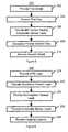
- FIG. 5is a high-level flow chart depicting one embodiment of a method 200 in accordance with the present invention for providing a MR head.
- the method 200is preferably used in fabricating the MR head 100 .
- the method 200is described in the context of the MR head 100 and the MR sensor 120 depicted in FIGS. 3A and 3B .
- a first shield 104 and a first gap 106are provided, via steps 202 and 204 , respectively.
- the MR sensor 120 having a composite sensor layer 128is provided, via step 206 .
- Step 206thus includes providing a CoFe layer 130 and a CoFeX layer 132 , each of which is preferably less than twenty Angstroms in thickness.
- the second gap 108is provided, via step 208 .
- the second shield 110is also provided, via step 210 .
- FIG. 6is a more detailed flow chart depicting one embodiment of a method for performing step 206 in accordance with the present invention for providing a magnetoresistive sensor 120 having a composite sensor layer.
- the method 206is preferably used in fabricating the MR head 100 . Thus, the method 206 is described in the context of the MR head 100 and the MR sensor 120 depicted in FIGS. 3A and 3B .
- the AFM layer 122is provided, via step 220 .
- the AFM layer 122may include PtMn.
- the pinned layer 124is provided, via step 222 .
- step 222includes providing two ferromagnetic layers 122 and 125 separated by an AFC layer 123 .
- step 222preferably provides a synthetic pinned layer.
- step 222can be used to provide a simple or other pinned layer.
- the nonmagnetic spacer layer 126which is preferably copper, is provided, via step 224 .
- the copper spacer layeris preferably treated by providing a trace of oxygen, preferably on the order of 10 ⁇ 4 mT, after deposition so that the CoFe/Cu interfaces are treated with a surfactant.
- the composite sensor layer 128is provided, via step 226 .
- Step 226thus includes providing a CoFe layer 130 that is preferably less than or equal to twenty Angstroms in thickness and a CoFeX layer 132 that is preferably less than twenty Angstroms in thickness.
- the capping layer 134is then provided, via step 228 .
- Step 228preferably includes providing the oxygen containing conductive layer 136 and a TaO layer 138 .
- the the conductive layer 136preferably includes a copper layer that contains a trace of oxygen diffused into through a thin TaO top layer 138 after deposition.
- the TaO layer 138is then provided on the conductive layer 136 .
- a MR head 100 and MR sensor 120 having a composite sensor layer 128can be provided.
- the composite sensor layer 128includes a CoFe layer 130 and a CoFeX layer 132 .
- Use of the composite sensorcan improve the soft magnetic properties of the MR sensor 120 , enhance the magnetoresistance ratio and improve magnetostriction. Thus, performance of the MR sensor 120 and the MR head 100 are improved.
Landscapes
- Engineering & Computer Science (AREA)
- Manufacturing & Machinery (AREA)
- Hall/Mr Elements (AREA)
Abstract
Description
| TABLE 1 | |||
| Magnetization | |||
| CoFeX (atomic %) | Structure | Resistivity (μΩcm) | (normalized) |
| X = 0 | fcc | 17.57 | 1.00 |
| X = Ti1Cu2 | fcc | 23.43 | .91 |
| X = B5 | fcc | 50.93 | .82 |
| X = Ta5 | fcc | 115.56 | .64 |
| TABLE 2 | |||||||
| Sensor Layer | Magneto- | λ | |||||
| (thickness, in magnetic | Rs | Resistance | Sens. | Hint | Hcf | Hk | (10−7 |
| moment equivalence) | (Ω/sq) | (%) | (%/Oe) | (Oe) | (Oe) | (Oe) | cm) |
| CoFe(13) | 21.2 | 13.7 | 1.13 | 2.73 | 3.77 | 8.44 | −17.8 |
| CoFe(11)/CoFeB(4) | 19.2 | 14.9 | 1.31 | 11.57 | 3.67 | 8.84 | 4.86 |
| CoFe(11)/CoFeTiCu(4) | 19.5 | 15.0 | 1.40 | 12.85 | 2.77 | 7.53 | −3.23 |
| CoFe(11)/CoFeTa(4) | 20.1 | 14.4 | 1.59 | 22.4 | 2.16 | 8.06 | −7.97 |
| CoFe(11)/COFeN(4) | 19.5 | 14.9 | 1.60 | 12.71 | 3.11 | 7.67 | −3.50 |
Claims (18)
Priority Applications (1)
| Application Number | Priority Date | Filing Date | Title |
|---|---|---|---|
| US10/349,470US6888704B1 (en) | 2003-01-22 | 2003-01-22 | Method and system for providing high sensitivity giant magnetoresistive sensors |
Applications Claiming Priority (1)
| Application Number | Priority Date | Filing Date | Title |
|---|---|---|---|
| US10/349,470US6888704B1 (en) | 2003-01-22 | 2003-01-22 | Method and system for providing high sensitivity giant magnetoresistive sensors |
Publications (1)
| Publication Number | Publication Date |
|---|---|
| US6888704B1true US6888704B1 (en) | 2005-05-03 |
Family
ID=34519838
Family Applications (1)
| Application Number | Title | Priority Date | Filing Date |
|---|---|---|---|
| US10/349,470Expired - LifetimeUS6888704B1 (en) | 2003-01-22 | 2003-01-22 | Method and system for providing high sensitivity giant magnetoresistive sensors |
Country Status (1)
| Country | Link |
|---|---|
| US (1) | US6888704B1 (en) |
Cited By (144)
| Publication number | Priority date | Publication date | Assignee | Title |
|---|---|---|---|---|
| US20040252416A1 (en)* | 2003-06-12 | 2004-12-16 | Headway Technologies, Inc. | Novel structure/method to form bottom spin valves for ultra-high density |
| US20060018057A1 (en)* | 2004-07-26 | 2006-01-26 | Yiming Huai | Magnetic tunnel junction having diffusion stop layer |
| US7224601B2 (en) | 2005-08-25 | 2007-05-29 | Grandis Inc. | Oscillating-field assisted spin torque switching of a magnetic tunnel junction memory element |
| US20070171694A1 (en)* | 2005-12-23 | 2007-07-26 | Yiming Huai | Current-switched spin-transfer magnetic devices with reduced spin-transfer switching current density |
| US20070246787A1 (en)* | 2006-03-29 | 2007-10-25 | Lien-Chang Wang | On-plug magnetic tunnel junction devices based on spin torque transfer switching |
| US20080061388A1 (en)* | 2006-09-13 | 2008-03-13 | Zhitao Diao | Devices and circuits based on magnetic tunnel junctions utilizing a multilayer barrier |
| US20080246103A1 (en)* | 2007-04-05 | 2008-10-09 | Headway Technologies, Inc. | MR device with surfactant layer within the free layer |
| US20090050991A1 (en)* | 2007-08-22 | 2009-02-26 | Hide Nagai | Magnetic Element Having Low Saturation Magnetization |
| US20100067293A1 (en)* | 2008-09-12 | 2010-03-18 | David Chang-Cheng Yu | Programmable and Redundant Circuitry Based On Magnetic Tunnel Junction (MTJ) |
| US20100072524A1 (en)* | 2005-09-20 | 2010-03-25 | Yiming Huai | Magnetic Devices Having Oxide Antiferromagnetic Layer Next To Free Ferromagnetic Layer |
| US20100073827A1 (en)* | 2008-09-22 | 2010-03-25 | Headway Technologies, Inc. | TMR device with novel free layer structure |
| US7777261B2 (en) | 2005-09-20 | 2010-08-17 | Grandis Inc. | Magnetic device having stabilized free ferromagnetic layer |
| US20100214835A1 (en)* | 2007-06-27 | 2010-08-26 | Yunfei Ding | Magnetic shielding in magnetic multilayer structures |
| US7973349B2 (en) | 2005-09-20 | 2011-07-05 | Grandis Inc. | Magnetic device having multilayered free ferromagnetic layer |
| US8830628B1 (en) | 2009-02-23 | 2014-09-09 | Western Digital (Fremont), Llc | Method and system for providing a perpendicular magnetic recording head |
| US8879207B1 (en) | 2011-12-20 | 2014-11-04 | Western Digital (Fremont), Llc | Method for providing a side shield for a magnetic recording transducer using an air bridge |
| US8883017B1 (en) | 2013-03-12 | 2014-11-11 | Western Digital (Fremont), Llc | Method and system for providing a read transducer having seamless interfaces |
| US8917581B1 (en) | 2013-12-18 | 2014-12-23 | Western Digital Technologies, Inc. | Self-anneal process for a near field transducer and chimney in a hard disk drive assembly |
| US8923102B1 (en) | 2013-07-16 | 2014-12-30 | Western Digital (Fremont), Llc | Optical grating coupling for interferometric waveguides in heat assisted magnetic recording heads |
| US8947985B1 (en) | 2013-07-16 | 2015-02-03 | Western Digital (Fremont), Llc | Heat assisted magnetic recording transducers having a recessed pole |
| US8953422B1 (en) | 2014-06-10 | 2015-02-10 | Western Digital (Fremont), Llc | Near field transducer using dielectric waveguide core with fine ridge feature |
| US8958272B1 (en) | 2014-06-10 | 2015-02-17 | Western Digital (Fremont), Llc | Interfering near field transducer for energy assisted magnetic recording |
| US8971160B1 (en) | 2013-12-19 | 2015-03-03 | Western Digital (Fremont), Llc | Near field transducer with high refractive index pin for heat assisted magnetic recording |
| US8970988B1 (en) | 2013-12-31 | 2015-03-03 | Western Digital (Fremont), Llc | Electric gaps and method for making electric gaps for multiple sensor arrays |
| US8976635B1 (en) | 2014-06-10 | 2015-03-10 | Western Digital (Fremont), Llc | Near field transducer driven by a transverse electric waveguide for energy assisted magnetic recording |
| US8982508B1 (en) | 2011-10-31 | 2015-03-17 | Western Digital (Fremont), Llc | Method for providing a side shield for a magnetic recording transducer |
| US8980109B1 (en) | 2012-12-11 | 2015-03-17 | Western Digital (Fremont), Llc | Method for providing a magnetic recording transducer using a combined main pole and side shield CMP for a wraparound shield scheme |
| US8988825B1 (en) | 2014-02-28 | 2015-03-24 | Western Digital (Fremont, LLC | Method for fabricating a magnetic writer having half-side shields |
| US8988812B1 (en) | 2013-11-27 | 2015-03-24 | Western Digital (Fremont), Llc | Multi-sensor array configuration for a two-dimensional magnetic recording (TDMR) operation |
| US8984740B1 (en) | 2012-11-30 | 2015-03-24 | Western Digital (Fremont), Llc | Process for providing a magnetic recording transducer having a smooth magnetic seed layer |
| US8995087B1 (en) | 2006-11-29 | 2015-03-31 | Western Digital (Fremont), Llc | Perpendicular magnetic recording write head having a wrap around shield |
| US8993217B1 (en) | 2013-04-04 | 2015-03-31 | Western Digital (Fremont), Llc | Double exposure technique for high resolution disk imaging |
| US9001628B1 (en) | 2013-12-16 | 2015-04-07 | Western Digital (Fremont), Llc | Assistant waveguides for evaluating main waveguide coupling efficiency and diode laser alignment tolerances for hard disk |
| US8997832B1 (en) | 2010-11-23 | 2015-04-07 | Western Digital (Fremont), Llc | Method of fabricating micrometer scale components |
| US9001467B1 (en) | 2014-03-05 | 2015-04-07 | Western Digital (Fremont), Llc | Method for fabricating side shields in a magnetic writer |
| US9007879B1 (en) | 2014-06-10 | 2015-04-14 | Western Digital (Fremont), Llc | Interfering near field transducer having a wide metal bar feature for energy assisted magnetic recording |
| US9007725B1 (en) | 2014-10-07 | 2015-04-14 | Western Digital (Fremont), Llc | Sensor with positive coupling between dual ferromagnetic free layer laminates |
| US9007719B1 (en) | 2013-10-23 | 2015-04-14 | Western Digital (Fremont), Llc | Systems and methods for using double mask techniques to achieve very small features |
| US9013836B1 (en) | 2013-04-02 | 2015-04-21 | Western Digital (Fremont), Llc | Method and system for providing an antiferromagnetically coupled return pole |
| US9042208B1 (en) | 2013-03-11 | 2015-05-26 | Western Digital Technologies, Inc. | Disk drive measuring fly height by applying a bias voltage to an electrically insulated write component of a head |
| US9042058B1 (en) | 2013-10-17 | 2015-05-26 | Western Digital Technologies, Inc. | Shield designed for middle shields in a multiple sensor array |
| US9042051B2 (en) | 2013-08-15 | 2015-05-26 | Western Digital (Fremont), Llc | Gradient write gap for perpendicular magnetic recording writer |
| US9042057B1 (en) | 2013-01-09 | 2015-05-26 | Western Digital (Fremont), Llc | Methods for providing magnetic storage elements with high magneto-resistance using Heusler alloys |
| US9042052B1 (en) | 2014-06-23 | 2015-05-26 | Western Digital (Fremont), Llc | Magnetic writer having a partially shunted coil |
| US9053735B1 (en) | 2014-06-20 | 2015-06-09 | Western Digital (Fremont), Llc | Method for fabricating a magnetic writer using a full-film metal planarization |
| US9064527B1 (en) | 2013-04-12 | 2015-06-23 | Western Digital (Fremont), Llc | High order tapered waveguide for use in a heat assisted magnetic recording head |
| US9064528B1 (en) | 2013-05-17 | 2015-06-23 | Western Digital Technologies, Inc. | Interferometric waveguide usable in shingled heat assisted magnetic recording in the absence of a near-field transducer |
| US9064507B1 (en) | 2009-07-31 | 2015-06-23 | Western Digital (Fremont), Llc | Magnetic etch-stop layer for magnetoresistive read heads |
| US9065043B1 (en) | 2012-06-29 | 2015-06-23 | Western Digital (Fremont), Llc | Tunnel magnetoresistance read head with narrow shield-to-shield spacing |
| US9070381B1 (en) | 2013-04-12 | 2015-06-30 | Western Digital (Fremont), Llc | Magnetic recording read transducer having a laminated free layer |
| US9082423B1 (en) | 2013-12-18 | 2015-07-14 | Western Digital (Fremont), Llc | Magnetic recording write transducer having an improved trailing surface profile |
| US9087527B1 (en) | 2014-10-28 | 2015-07-21 | Western Digital (Fremont), Llc | Apparatus and method for middle shield connection in magnetic recording transducers |
| US9087534B1 (en) | 2011-12-20 | 2015-07-21 | Western Digital (Fremont), Llc | Method and system for providing a read transducer having soft and hard magnetic bias structures |
| US9093639B2 (en) | 2012-02-21 | 2015-07-28 | Western Digital (Fremont), Llc | Methods for manufacturing a magnetoresistive structure utilizing heating and cooling |
| US9104107B1 (en) | 2013-04-03 | 2015-08-11 | Western Digital (Fremont), Llc | DUV photoresist process |
| US9111550B1 (en) | 2014-12-04 | 2015-08-18 | Western Digital (Fremont), Llc | Write transducer having a magnetic buffer layer spaced between a side shield and a write pole by non-magnetic layers |
| US9111558B1 (en) | 2014-03-14 | 2015-08-18 | Western Digital (Fremont), Llc | System and method of diffractive focusing of light in a waveguide |
| US9111564B1 (en) | 2013-04-02 | 2015-08-18 | Western Digital (Fremont), Llc | Magnetic recording writer having a main pole with multiple flare angles |
| US9123362B1 (en) | 2011-03-22 | 2015-09-01 | Western Digital (Fremont), Llc | Methods for assembling an electrically assisted magnetic recording (EAMR) head |
| US9123359B1 (en) | 2010-12-22 | 2015-09-01 | Western Digital (Fremont), Llc | Magnetic recording transducer with sputtered antiferromagnetic coupling trilayer between plated ferromagnetic shields and method of fabrication |
| US9123374B1 (en) | 2015-02-12 | 2015-09-01 | Western Digital (Fremont), Llc | Heat assisted magnetic recording writer having an integrated polarization rotation plate |
| US9123358B1 (en) | 2012-06-11 | 2015-09-01 | Western Digital (Fremont), Llc | Conformal high moment side shield seed layer for perpendicular magnetic recording writer |
| US9135930B1 (en) | 2014-03-06 | 2015-09-15 | Western Digital (Fremont), Llc | Method for fabricating a magnetic write pole using vacuum deposition |
| US9135937B1 (en) | 2014-05-09 | 2015-09-15 | Western Digital (Fremont), Llc | Current modulation on laser diode for energy assisted magnetic recording transducer |
| US9142233B1 (en) | 2014-02-28 | 2015-09-22 | Western Digital (Fremont), Llc | Heat assisted magnetic recording writer having a recessed pole |
| US9147404B1 (en) | 2015-03-31 | 2015-09-29 | Western Digital (Fremont), Llc | Method and system for providing a read transducer having a dual free layer |
| US9147408B1 (en) | 2013-12-19 | 2015-09-29 | Western Digital (Fremont), Llc | Heated AFM layer deposition and cooling process for TMR magnetic recording sensor with high pinning field |
| US9153255B1 (en) | 2014-03-05 | 2015-10-06 | Western Digital (Fremont), Llc | Method for fabricating a magnetic writer having an asymmetric gap and shields |
| US9183854B2 (en) | 2014-02-24 | 2015-11-10 | Western Digital (Fremont), Llc | Method to make interferometric taper waveguide for HAMR light delivery |
| US9190085B1 (en) | 2014-03-12 | 2015-11-17 | Western Digital (Fremont), Llc | Waveguide with reflective grating for localized energy intensity |
| US9190079B1 (en) | 2014-09-22 | 2015-11-17 | Western Digital (Fremont), Llc | Magnetic write pole having engineered radius of curvature and chisel angle profiles |
| US9194692B1 (en) | 2013-12-06 | 2015-11-24 | Western Digital (Fremont), Llc | Systems and methods for using white light interferometry to measure undercut of a bi-layer structure |
| US9202480B2 (en) | 2009-10-14 | 2015-12-01 | Western Digital (Fremont), LLC. | Double patterning hard mask for damascene perpendicular magnetic recording (PMR) writer |
| US9202493B1 (en) | 2014-02-28 | 2015-12-01 | Western Digital (Fremont), Llc | Method of making an ultra-sharp tip mode converter for a HAMR head |
| US9213322B1 (en) | 2012-08-16 | 2015-12-15 | Western Digital (Fremont), Llc | Methods for providing run to run process control using a dynamic tuner |
| US9214165B1 (en) | 2014-12-18 | 2015-12-15 | Western Digital (Fremont), Llc | Magnetic writer having a gradient in saturation magnetization of the shields |
| US9214169B1 (en) | 2014-06-20 | 2015-12-15 | Western Digital (Fremont), Llc | Magnetic recording read transducer having a laminated free layer |
| US9214172B2 (en) | 2013-10-23 | 2015-12-15 | Western Digital (Fremont), Llc | Method of manufacturing a magnetic read head |
| US9230565B1 (en) | 2014-06-24 | 2016-01-05 | Western Digital (Fremont), Llc | Magnetic shield for magnetic recording head |
| US9236560B1 (en) | 2014-12-08 | 2016-01-12 | Western Digital (Fremont), Llc | Spin transfer torque tunneling magnetoresistive device having a laminated free layer with perpendicular magnetic anisotropy |
| US9245562B1 (en) | 2015-03-30 | 2016-01-26 | Western Digital (Fremont), Llc | Magnetic recording writer with a composite main pole |
| US9245543B1 (en) | 2010-06-25 | 2016-01-26 | Western Digital (Fremont), Llc | Method for providing an energy assisted magnetic recording head having a laser integrally mounted to the slider |
| US9245545B1 (en) | 2013-04-12 | 2016-01-26 | Wester Digital (Fremont), Llc | Short yoke length coils for magnetic heads in disk drives |
| US9251813B1 (en) | 2009-04-19 | 2016-02-02 | Western Digital (Fremont), Llc | Method of making a magnetic recording head |
| US9263071B1 (en) | 2015-03-31 | 2016-02-16 | Western Digital (Fremont), Llc | Flat NFT for heat assisted magnetic recording |
| US9263067B1 (en) | 2013-05-29 | 2016-02-16 | Western Digital (Fremont), Llc | Process for making PMR writer with constant side wall angle |
| US9269382B1 (en) | 2012-06-29 | 2016-02-23 | Western Digital (Fremont), Llc | Method and system for providing a read transducer having improved pinning of the pinned layer at higher recording densities |
| US9275657B1 (en) | 2013-08-14 | 2016-03-01 | Western Digital (Fremont), Llc | Process for making PMR writer with non-conformal side gaps |
| US9280990B1 (en) | 2013-12-11 | 2016-03-08 | Western Digital (Fremont), Llc | Method for fabricating a magnetic writer using multiple etches |
| US9287494B1 (en) | 2013-06-28 | 2016-03-15 | Western Digital (Fremont), Llc | Magnetic tunnel junction (MTJ) with a magnesium oxide tunnel barrier |
| US9286919B1 (en) | 2014-12-17 | 2016-03-15 | Western Digital (Fremont), Llc | Magnetic writer having a dual side gap |
| US9305583B1 (en) | 2014-02-18 | 2016-04-05 | Western Digital (Fremont), Llc | Method for fabricating a magnetic writer using multiple etches of damascene materials |
| US9312064B1 (en) | 2015-03-02 | 2016-04-12 | Western Digital (Fremont), Llc | Method to fabricate a magnetic head including ion milling of read gap using dual layer hard mask |
| US9318130B1 (en) | 2013-07-02 | 2016-04-19 | Western Digital (Fremont), Llc | Method to fabricate tunneling magnetic recording heads with extended pinned layer |
| US9336814B1 (en) | 2013-03-12 | 2016-05-10 | Western Digital (Fremont), Llc | Inverse tapered waveguide for use in a heat assisted magnetic recording head |
| US9343098B1 (en) | 2013-08-23 | 2016-05-17 | Western Digital (Fremont), Llc | Method for providing a heat assisted magnetic recording transducer having protective pads |
| US9343086B1 (en) | 2013-09-11 | 2016-05-17 | Western Digital (Fremont), Llc | Magnetic recording write transducer having an improved sidewall angle profile |
| US9343087B1 (en) | 2014-12-21 | 2016-05-17 | Western Digital (Fremont), Llc | Method for fabricating a magnetic writer having half shields |
| US9349394B1 (en) | 2013-10-18 | 2016-05-24 | Western Digital (Fremont), Llc | Method for fabricating a magnetic writer having a gradient side gap |
| US9349392B1 (en) | 2012-05-24 | 2016-05-24 | Western Digital (Fremont), Llc | Methods for improving adhesion on dielectric substrates |
| US9361914B1 (en) | 2014-06-18 | 2016-06-07 | Western Digital (Fremont), Llc | Magnetic sensor with thin capping layer |
| US9361913B1 (en) | 2013-06-03 | 2016-06-07 | Western Digital (Fremont), Llc | Recording read heads with a multi-layer AFM layer methods and apparatuses |
| US9368134B1 (en) | 2010-12-16 | 2016-06-14 | Western Digital (Fremont), Llc | Method and system for providing an antiferromagnetically coupled writer |
| US9384763B1 (en) | 2015-03-26 | 2016-07-05 | Western Digital (Fremont), Llc | Dual free layer magnetic reader having a rear bias structure including a soft bias layer |
| US9384765B1 (en) | 2015-09-24 | 2016-07-05 | Western Digital (Fremont), Llc | Method and system for providing a HAMR writer having improved optical efficiency |
| US9396742B1 (en) | 2012-11-30 | 2016-07-19 | Western Digital (Fremont), Llc | Magnetoresistive sensor for a magnetic storage system read head, and fabrication method thereof |
| US9396743B1 (en) | 2014-02-28 | 2016-07-19 | Western Digital (Fremont), Llc | Systems and methods for controlling soft bias thickness for tunnel magnetoresistance readers |
| US9406331B1 (en) | 2013-06-17 | 2016-08-02 | Western Digital (Fremont), Llc | Method for making ultra-narrow read sensor and read transducer device resulting therefrom |
| US9424866B1 (en) | 2015-09-24 | 2016-08-23 | Western Digital (Fremont), Llc | Heat assisted magnetic recording write apparatus having a dielectric gap |
| US9431031B1 (en) | 2015-03-24 | 2016-08-30 | Western Digital (Fremont), Llc | System and method for magnetic transducers having multiple sensors and AFC shields |
| US9431038B1 (en) | 2015-06-29 | 2016-08-30 | Western Digital (Fremont), Llc | Method for fabricating a magnetic write pole having an improved sidewall angle profile |
| US9431047B1 (en) | 2013-05-01 | 2016-08-30 | Western Digital (Fremont), Llc | Method for providing an improved AFM reader shield |
| US9431039B1 (en) | 2013-05-21 | 2016-08-30 | Western Digital (Fremont), Llc | Multiple sensor array usable in two-dimensional magnetic recording |
| US9431032B1 (en) | 2013-08-14 | 2016-08-30 | Western Digital (Fremont), Llc | Electrical connection arrangement for a multiple sensor array usable in two-dimensional magnetic recording |
| US9437251B1 (en) | 2014-12-22 | 2016-09-06 | Western Digital (Fremont), Llc | Apparatus and method having TDMR reader to reader shunts |
| US9443541B1 (en) | 2015-03-24 | 2016-09-13 | Western Digital (Fremont), Llc | Magnetic writer having a gradient in saturation magnetization of the shields and return pole |
| US9441938B1 (en) | 2013-10-08 | 2016-09-13 | Western Digital (Fremont), Llc | Test structures for measuring near field transducer disc length |
| US9449621B1 (en) | 2015-03-26 | 2016-09-20 | Western Digital (Fremont), Llc | Dual free layer magnetic reader having a rear bias structure having a high aspect ratio |
| US9449625B1 (en) | 2014-12-24 | 2016-09-20 | Western Digital (Fremont), Llc | Heat assisted magnetic recording head having a plurality of diffusion barrier layers |
| US9472216B1 (en) | 2015-09-23 | 2016-10-18 | Western Digital (Fremont), Llc | Differential dual free layer magnetic reader |
| US9484051B1 (en) | 2015-11-09 | 2016-11-01 | The Provost, Fellows, Foundation Scholars and the other members of Board, of the College of the Holy and Undivided Trinity of Queen Elizabeth near Dublin | Method and system for reducing undesirable reflections in a HAMR write apparatus |
| US9508363B1 (en) | 2014-06-17 | 2016-11-29 | Western Digital (Fremont), Llc | Method for fabricating a magnetic write pole having a leading edge bevel |
| US9508365B1 (en) | 2015-06-24 | 2016-11-29 | Western Digital (Fremont), LLC. | Magnetic reader having a crystal decoupling structure |
| US9508372B1 (en) | 2015-06-03 | 2016-11-29 | Western Digital (Fremont), Llc | Shingle magnetic writer having a low sidewall angle pole |
| US9530443B1 (en) | 2015-06-25 | 2016-12-27 | Western Digital (Fremont), Llc | Method for fabricating a magnetic recording device having a high aspect ratio structure |
| US9564150B1 (en) | 2015-11-24 | 2017-02-07 | Western Digital (Fremont), Llc | Magnetic read apparatus having an improved read sensor isolation circuit |
| US9595273B1 (en) | 2015-09-30 | 2017-03-14 | Western Digital (Fremont), Llc | Shingle magnetic writer having nonconformal shields |
| US9646639B2 (en) | 2015-06-26 | 2017-05-09 | Western Digital (Fremont), Llc | Heat assisted magnetic recording writer having integrated polarization rotation waveguides |
| US9666214B1 (en) | 2015-09-23 | 2017-05-30 | Western Digital (Fremont), Llc | Free layer magnetic reader that may have a reduced shield-to-shield spacing |
| US9721595B1 (en) | 2014-12-04 | 2017-08-01 | Western Digital (Fremont), Llc | Method for providing a storage device |
| US9741366B1 (en) | 2014-12-18 | 2017-08-22 | Western Digital (Fremont), Llc | Method for fabricating a magnetic writer having a gradient in saturation magnetization of the shields |
| US9740805B1 (en) | 2015-12-01 | 2017-08-22 | Western Digital (Fremont), Llc | Method and system for detecting hotspots for photolithographically-defined devices |
| US9754611B1 (en) | 2015-11-30 | 2017-09-05 | Western Digital (Fremont), Llc | Magnetic recording write apparatus having a stepped conformal trailing shield |
| US9767831B1 (en) | 2015-12-01 | 2017-09-19 | Western Digital (Fremont), Llc | Magnetic writer having convex trailing surface pole and conformal write gap |
| US9786301B1 (en) | 2014-12-02 | 2017-10-10 | Western Digital (Fremont), Llc | Apparatuses and methods for providing thin shields in a multiple sensor array |
| US9799351B1 (en) | 2015-11-30 | 2017-10-24 | Western Digital (Fremont), Llc | Short yoke length writer having assist coils |
| US9812155B1 (en) | 2015-11-23 | 2017-11-07 | Western Digital (Fremont), Llc | Method and system for fabricating high junction angle read sensors |
| US9842615B1 (en) | 2015-06-26 | 2017-12-12 | Western Digital (Fremont), Llc | Magnetic reader having a nonmagnetic insertion layer for the pinning layer |
| US9858951B1 (en) | 2015-12-01 | 2018-01-02 | Western Digital (Fremont), Llc | Method for providing a multilayer AFM layer in a read sensor |
| US9881638B1 (en) | 2014-12-17 | 2018-01-30 | Western Digital (Fremont), Llc | Method for providing a near-field transducer (NFT) for a heat assisted magnetic recording (HAMR) device |
| US9934811B1 (en) | 2014-03-07 | 2018-04-03 | Western Digital (Fremont), Llc | Methods for controlling stray fields of magnetic features using magneto-elastic anisotropy |
| US9953670B1 (en) | 2015-11-10 | 2018-04-24 | Western Digital (Fremont), Llc | Method and system for providing a HAMR writer including a multi-mode interference device |
| US10037770B1 (en) | 2015-11-12 | 2018-07-31 | Western Digital (Fremont), Llc | Method for providing a magnetic recording write apparatus having a seamless pole |
| US10074387B1 (en) | 2014-12-21 | 2018-09-11 | Western Digital (Fremont), Llc | Method and system for providing a read transducer having symmetric antiferromagnetically coupled shields |
Citations (5)
| Publication number | Priority date | Publication date | Assignee | Title |
|---|---|---|---|---|
| US6249406B1 (en)* | 1996-09-23 | 2001-06-19 | International Business Machines Corporation | Magnetoresistive sensor with a soft adjacent layer having high magnetization, high resistivity, low intrinsic anisotropy and near zero magnetostriction |
| US6381106B1 (en)* | 2000-04-12 | 2002-04-30 | International Business Machines Corporation | Top spin valve sensor that has a free layer structure with a cobalt iron boron (cofeb) layer |
| US20030123201A1 (en)* | 2002-01-02 | 2003-07-03 | International Business Machines Corporation | Method and apparatus for providing precise control of magnetic coupling field in NiMn top spin valve heads and amplitude enhancement |
| US6614630B2 (en)* | 2001-04-23 | 2003-09-02 | Headway Technologies, Inc. | Top spin valve heads for ultra-high recording density |
| US6624985B1 (en)* | 2002-01-07 | 2003-09-23 | International Business Machines Corporation | Pinning layer seeds for CPP geometry spin valve sensors |
- 2003
- 2003-01-22USUS10/349,470patent/US6888704B1/ennot_activeExpired - Lifetime
Patent Citations (5)
| Publication number | Priority date | Publication date | Assignee | Title |
|---|---|---|---|---|
| US6249406B1 (en)* | 1996-09-23 | 2001-06-19 | International Business Machines Corporation | Magnetoresistive sensor with a soft adjacent layer having high magnetization, high resistivity, low intrinsic anisotropy and near zero magnetostriction |
| US6381106B1 (en)* | 2000-04-12 | 2002-04-30 | International Business Machines Corporation | Top spin valve sensor that has a free layer structure with a cobalt iron boron (cofeb) layer |
| US6614630B2 (en)* | 2001-04-23 | 2003-09-02 | Headway Technologies, Inc. | Top spin valve heads for ultra-high recording density |
| US20030123201A1 (en)* | 2002-01-02 | 2003-07-03 | International Business Machines Corporation | Method and apparatus for providing precise control of magnetic coupling field in NiMn top spin valve heads and amplitude enhancement |
| US6624985B1 (en)* | 2002-01-07 | 2003-09-23 | International Business Machines Corporation | Pinning layer seeds for CPP geometry spin valve sensors |
Cited By (173)
| Publication number | Priority date | Publication date | Assignee | Title |
|---|---|---|---|---|
| US20040252416A1 (en)* | 2003-06-12 | 2004-12-16 | Headway Technologies, Inc. | Novel structure/method to form bottom spin valves for ultra-high density |
| US7042684B2 (en)* | 2003-06-12 | 2006-05-09 | Headway Technologies, Inc. | Structure/method to form bottom spin valves for ultra-high density |
| US20060018057A1 (en)* | 2004-07-26 | 2006-01-26 | Yiming Huai | Magnetic tunnel junction having diffusion stop layer |
| US7576956B2 (en) | 2004-07-26 | 2009-08-18 | Grandis Inc. | Magnetic tunnel junction having diffusion stop layer |
| US7224601B2 (en) | 2005-08-25 | 2007-05-29 | Grandis Inc. | Oscillating-field assisted spin torque switching of a magnetic tunnel junction memory element |
| US7973349B2 (en) | 2005-09-20 | 2011-07-05 | Grandis Inc. | Magnetic device having multilayered free ferromagnetic layer |
| US7859034B2 (en) | 2005-09-20 | 2010-12-28 | Grandis Inc. | Magnetic devices having oxide antiferromagnetic layer next to free ferromagnetic layer |
| US7777261B2 (en) | 2005-09-20 | 2010-08-17 | Grandis Inc. | Magnetic device having stabilized free ferromagnetic layer |
| US20100072524A1 (en)* | 2005-09-20 | 2010-03-25 | Yiming Huai | Magnetic Devices Having Oxide Antiferromagnetic Layer Next To Free Ferromagnetic Layer |
| US20070171694A1 (en)* | 2005-12-23 | 2007-07-26 | Yiming Huai | Current-switched spin-transfer magnetic devices with reduced spin-transfer switching current density |
| US7430135B2 (en) | 2005-12-23 | 2008-09-30 | Grandis Inc. | Current-switched spin-transfer magnetic devices with reduced spin-transfer switching current density |
| US20070246787A1 (en)* | 2006-03-29 | 2007-10-25 | Lien-Chang Wang | On-plug magnetic tunnel junction devices based on spin torque transfer switching |
| US7851840B2 (en) | 2006-09-13 | 2010-12-14 | Grandis Inc. | Devices and circuits based on magnetic tunnel junctions utilizing a multilayer barrier |
| US20080061388A1 (en)* | 2006-09-13 | 2008-03-13 | Zhitao Diao | Devices and circuits based on magnetic tunnel junctions utilizing a multilayer barrier |
| US8995087B1 (en) | 2006-11-29 | 2015-03-31 | Western Digital (Fremont), Llc | Perpendicular magnetic recording write head having a wrap around shield |
| US20080246103A1 (en)* | 2007-04-05 | 2008-10-09 | Headway Technologies, Inc. | MR device with surfactant layer within the free layer |
| US8213221B2 (en) | 2007-06-27 | 2012-07-03 | Grandis, Inc. | Magnetic shielding in magnetic multilayer structures |
| US20100214835A1 (en)* | 2007-06-27 | 2010-08-26 | Yunfei Ding | Magnetic shielding in magnetic multilayer structures |
| US20110210410A1 (en)* | 2007-06-27 | 2011-09-01 | Grandis Inc. | Magnetic shielding in magnetic multilayer structures |
| US7957179B2 (en) | 2007-06-27 | 2011-06-07 | Grandis Inc. | Magnetic shielding in magnetic multilayer structures |
| US8476723B2 (en) | 2007-08-22 | 2013-07-02 | Grandis, Inc. | Magnetic element having low saturation magnetization |
| US20090050991A1 (en)* | 2007-08-22 | 2009-02-26 | Hide Nagai | Magnetic Element Having Low Saturation Magnetization |
| US7982275B2 (en) | 2007-08-22 | 2011-07-19 | Grandis Inc. | Magnetic element having low saturation magnetization |
| US7894248B2 (en) | 2008-09-12 | 2011-02-22 | Grandis Inc. | Programmable and redundant circuitry based on magnetic tunnel junction (MTJ) |
| US20100067293A1 (en)* | 2008-09-12 | 2010-03-18 | David Chang-Cheng Yu | Programmable and Redundant Circuitry Based On Magnetic Tunnel Junction (MTJ) |
| US9040178B2 (en)* | 2008-09-22 | 2015-05-26 | Headway Technologies, Inc. | TMR device with novel free layer structure |
| US20100073827A1 (en)* | 2008-09-22 | 2010-03-25 | Headway Technologies, Inc. | TMR device with novel free layer structure |
| US20150249210A1 (en)* | 2008-09-22 | 2015-09-03 | Headway Technologies, Inc. | TMR Device with Novel Free Layer Structure |
| US9437812B2 (en)* | 2008-09-22 | 2016-09-06 | Headway Technologies, Inc. | TMR device with novel free layer structure |
| US8830628B1 (en) | 2009-02-23 | 2014-09-09 | Western Digital (Fremont), Llc | Method and system for providing a perpendicular magnetic recording head |
| US9251813B1 (en) | 2009-04-19 | 2016-02-02 | Western Digital (Fremont), Llc | Method of making a magnetic recording head |
| US9064507B1 (en) | 2009-07-31 | 2015-06-23 | Western Digital (Fremont), Llc | Magnetic etch-stop layer for magnetoresistive read heads |
| US9202480B2 (en) | 2009-10-14 | 2015-12-01 | Western Digital (Fremont), LLC. | Double patterning hard mask for damascene perpendicular magnetic recording (PMR) writer |
| US9245543B1 (en) | 2010-06-25 | 2016-01-26 | Western Digital (Fremont), Llc | Method for providing an energy assisted magnetic recording head having a laser integrally mounted to the slider |
| US9672847B2 (en) | 2010-11-23 | 2017-06-06 | Western Digital (Fremont), Llc | Micrometer scale components |
| US8997832B1 (en) | 2010-11-23 | 2015-04-07 | Western Digital (Fremont), Llc | Method of fabricating micrometer scale components |
| US9159345B1 (en) | 2010-11-23 | 2015-10-13 | Western Digital (Fremont), Llc | Micrometer scale components |
| US9368134B1 (en) | 2010-12-16 | 2016-06-14 | Western Digital (Fremont), Llc | Method and system for providing an antiferromagnetically coupled writer |
| US9123359B1 (en) | 2010-12-22 | 2015-09-01 | Western Digital (Fremont), Llc | Magnetic recording transducer with sputtered antiferromagnetic coupling trilayer between plated ferromagnetic shields and method of fabrication |
| US9123362B1 (en) | 2011-03-22 | 2015-09-01 | Western Digital (Fremont), Llc | Methods for assembling an electrically assisted magnetic recording (EAMR) head |
| US8982508B1 (en) | 2011-10-31 | 2015-03-17 | Western Digital (Fremont), Llc | Method for providing a side shield for a magnetic recording transducer |
| US9087534B1 (en) | 2011-12-20 | 2015-07-21 | Western Digital (Fremont), Llc | Method and system for providing a read transducer having soft and hard magnetic bias structures |
| US8879207B1 (en) | 2011-12-20 | 2014-11-04 | Western Digital (Fremont), Llc | Method for providing a side shield for a magnetic recording transducer using an air bridge |
| US9093639B2 (en) | 2012-02-21 | 2015-07-28 | Western Digital (Fremont), Llc | Methods for manufacturing a magnetoresistive structure utilizing heating and cooling |
| US9349392B1 (en) | 2012-05-24 | 2016-05-24 | Western Digital (Fremont), Llc | Methods for improving adhesion on dielectric substrates |
| US9123358B1 (en) | 2012-06-11 | 2015-09-01 | Western Digital (Fremont), Llc | Conformal high moment side shield seed layer for perpendicular magnetic recording writer |
| US9269382B1 (en) | 2012-06-29 | 2016-02-23 | Western Digital (Fremont), Llc | Method and system for providing a read transducer having improved pinning of the pinned layer at higher recording densities |
| US9412400B2 (en) | 2012-06-29 | 2016-08-09 | Western Digital (Fremont), Llc | Tunnel magnetoresistance read head with narrow shield-to-shield spacing |
| US9065043B1 (en) | 2012-06-29 | 2015-06-23 | Western Digital (Fremont), Llc | Tunnel magnetoresistance read head with narrow shield-to-shield spacing |
| US9213322B1 (en) | 2012-08-16 | 2015-12-15 | Western Digital (Fremont), Llc | Methods for providing run to run process control using a dynamic tuner |
| US9396742B1 (en) | 2012-11-30 | 2016-07-19 | Western Digital (Fremont), Llc | Magnetoresistive sensor for a magnetic storage system read head, and fabrication method thereof |
| US8984740B1 (en) | 2012-11-30 | 2015-03-24 | Western Digital (Fremont), Llc | Process for providing a magnetic recording transducer having a smooth magnetic seed layer |
| US8980109B1 (en) | 2012-12-11 | 2015-03-17 | Western Digital (Fremont), Llc | Method for providing a magnetic recording transducer using a combined main pole and side shield CMP for a wraparound shield scheme |
| US9042057B1 (en) | 2013-01-09 | 2015-05-26 | Western Digital (Fremont), Llc | Methods for providing magnetic storage elements with high magneto-resistance using Heusler alloys |
| US9042208B1 (en) | 2013-03-11 | 2015-05-26 | Western Digital Technologies, Inc. | Disk drive measuring fly height by applying a bias voltage to an electrically insulated write component of a head |
| US8883017B1 (en) | 2013-03-12 | 2014-11-11 | Western Digital (Fremont), Llc | Method and system for providing a read transducer having seamless interfaces |
| US9336814B1 (en) | 2013-03-12 | 2016-05-10 | Western Digital (Fremont), Llc | Inverse tapered waveguide for use in a heat assisted magnetic recording head |
| US9013836B1 (en) | 2013-04-02 | 2015-04-21 | Western Digital (Fremont), Llc | Method and system for providing an antiferromagnetically coupled return pole |
| US9111564B1 (en) | 2013-04-02 | 2015-08-18 | Western Digital (Fremont), Llc | Magnetic recording writer having a main pole with multiple flare angles |
| US9104107B1 (en) | 2013-04-03 | 2015-08-11 | Western Digital (Fremont), Llc | DUV photoresist process |
| US8993217B1 (en) | 2013-04-04 | 2015-03-31 | Western Digital (Fremont), Llc | Double exposure technique for high resolution disk imaging |
| US9245545B1 (en) | 2013-04-12 | 2016-01-26 | Wester Digital (Fremont), Llc | Short yoke length coils for magnetic heads in disk drives |
| US9070381B1 (en) | 2013-04-12 | 2015-06-30 | Western Digital (Fremont), Llc | Magnetic recording read transducer having a laminated free layer |
| US9064527B1 (en) | 2013-04-12 | 2015-06-23 | Western Digital (Fremont), Llc | High order tapered waveguide for use in a heat assisted magnetic recording head |
| US9431047B1 (en) | 2013-05-01 | 2016-08-30 | Western Digital (Fremont), Llc | Method for providing an improved AFM reader shield |
| US9064528B1 (en) | 2013-05-17 | 2015-06-23 | Western Digital Technologies, Inc. | Interferometric waveguide usable in shingled heat assisted magnetic recording in the absence of a near-field transducer |
| US9431039B1 (en) | 2013-05-21 | 2016-08-30 | Western Digital (Fremont), Llc | Multiple sensor array usable in two-dimensional magnetic recording |
| US9263067B1 (en) | 2013-05-29 | 2016-02-16 | Western Digital (Fremont), Llc | Process for making PMR writer with constant side wall angle |
| US9361913B1 (en) | 2013-06-03 | 2016-06-07 | Western Digital (Fremont), Llc | Recording read heads with a multi-layer AFM layer methods and apparatuses |
| US9406331B1 (en) | 2013-06-17 | 2016-08-02 | Western Digital (Fremont), Llc | Method for making ultra-narrow read sensor and read transducer device resulting therefrom |
| US9287494B1 (en) | 2013-06-28 | 2016-03-15 | Western Digital (Fremont), Llc | Magnetic tunnel junction (MTJ) with a magnesium oxide tunnel barrier |
| US9318130B1 (en) | 2013-07-02 | 2016-04-19 | Western Digital (Fremont), Llc | Method to fabricate tunneling magnetic recording heads with extended pinned layer |
| US8923102B1 (en) | 2013-07-16 | 2014-12-30 | Western Digital (Fremont), Llc | Optical grating coupling for interferometric waveguides in heat assisted magnetic recording heads |
| US8947985B1 (en) | 2013-07-16 | 2015-02-03 | Western Digital (Fremont), Llc | Heat assisted magnetic recording transducers having a recessed pole |
| US9431032B1 (en) | 2013-08-14 | 2016-08-30 | Western Digital (Fremont), Llc | Electrical connection arrangement for a multiple sensor array usable in two-dimensional magnetic recording |
| US9275657B1 (en) | 2013-08-14 | 2016-03-01 | Western Digital (Fremont), Llc | Process for making PMR writer with non-conformal side gaps |
| US9042051B2 (en) | 2013-08-15 | 2015-05-26 | Western Digital (Fremont), Llc | Gradient write gap for perpendicular magnetic recording writer |
| US9343098B1 (en) | 2013-08-23 | 2016-05-17 | Western Digital (Fremont), Llc | Method for providing a heat assisted magnetic recording transducer having protective pads |
| US9343086B1 (en) | 2013-09-11 | 2016-05-17 | Western Digital (Fremont), Llc | Magnetic recording write transducer having an improved sidewall angle profile |
| US9441938B1 (en) | 2013-10-08 | 2016-09-13 | Western Digital (Fremont), Llc | Test structures for measuring near field transducer disc length |
| US9042058B1 (en) | 2013-10-17 | 2015-05-26 | Western Digital Technologies, Inc. | Shield designed for middle shields in a multiple sensor array |
| US9349394B1 (en) | 2013-10-18 | 2016-05-24 | Western Digital (Fremont), Llc | Method for fabricating a magnetic writer having a gradient side gap |
| US9830936B2 (en) | 2013-10-23 | 2017-11-28 | Western Digital (Fremont), Llc | Magnetic read head with antiferromagentic layer |
| US9007719B1 (en) | 2013-10-23 | 2015-04-14 | Western Digital (Fremont), Llc | Systems and methods for using double mask techniques to achieve very small features |
| US9214172B2 (en) | 2013-10-23 | 2015-12-15 | Western Digital (Fremont), Llc | Method of manufacturing a magnetic read head |
| US8988812B1 (en) | 2013-11-27 | 2015-03-24 | Western Digital (Fremont), Llc | Multi-sensor array configuration for a two-dimensional magnetic recording (TDMR) operation |
| US9194692B1 (en) | 2013-12-06 | 2015-11-24 | Western Digital (Fremont), Llc | Systems and methods for using white light interferometry to measure undercut of a bi-layer structure |
| US9280990B1 (en) | 2013-12-11 | 2016-03-08 | Western Digital (Fremont), Llc | Method for fabricating a magnetic writer using multiple etches |
| US9001628B1 (en) | 2013-12-16 | 2015-04-07 | Western Digital (Fremont), Llc | Assistant waveguides for evaluating main waveguide coupling efficiency and diode laser alignment tolerances for hard disk |
| US8917581B1 (en) | 2013-12-18 | 2014-12-23 | Western Digital Technologies, Inc. | Self-anneal process for a near field transducer and chimney in a hard disk drive assembly |
| US9082423B1 (en) | 2013-12-18 | 2015-07-14 | Western Digital (Fremont), Llc | Magnetic recording write transducer having an improved trailing surface profile |
| US8971160B1 (en) | 2013-12-19 | 2015-03-03 | Western Digital (Fremont), Llc | Near field transducer with high refractive index pin for heat assisted magnetic recording |
| US9147408B1 (en) | 2013-12-19 | 2015-09-29 | Western Digital (Fremont), Llc | Heated AFM layer deposition and cooling process for TMR magnetic recording sensor with high pinning field |
| US8970988B1 (en) | 2013-12-31 | 2015-03-03 | Western Digital (Fremont), Llc | Electric gaps and method for making electric gaps for multiple sensor arrays |
| US9305583B1 (en) | 2014-02-18 | 2016-04-05 | Western Digital (Fremont), Llc | Method for fabricating a magnetic writer using multiple etches of damascene materials |
| US9183854B2 (en) | 2014-02-24 | 2015-11-10 | Western Digital (Fremont), Llc | Method to make interferometric taper waveguide for HAMR light delivery |
| US9396743B1 (en) | 2014-02-28 | 2016-07-19 | Western Digital (Fremont), Llc | Systems and methods for controlling soft bias thickness for tunnel magnetoresistance readers |
| US9202493B1 (en) | 2014-02-28 | 2015-12-01 | Western Digital (Fremont), Llc | Method of making an ultra-sharp tip mode converter for a HAMR head |
| US9142233B1 (en) | 2014-02-28 | 2015-09-22 | Western Digital (Fremont), Llc | Heat assisted magnetic recording writer having a recessed pole |
| US8988825B1 (en) | 2014-02-28 | 2015-03-24 | Western Digital (Fremont, LLC | Method for fabricating a magnetic writer having half-side shields |
| US9001467B1 (en) | 2014-03-05 | 2015-04-07 | Western Digital (Fremont), Llc | Method for fabricating side shields in a magnetic writer |
| US9349393B2 (en) | 2014-03-05 | 2016-05-24 | Western Digital (Fremont), Llc | Magnetic writer having an asymmetric gap and shields |
| US9153255B1 (en) | 2014-03-05 | 2015-10-06 | Western Digital (Fremont), Llc | Method for fabricating a magnetic writer having an asymmetric gap and shields |
| US9135930B1 (en) | 2014-03-06 | 2015-09-15 | Western Digital (Fremont), Llc | Method for fabricating a magnetic write pole using vacuum deposition |
| US9934811B1 (en) | 2014-03-07 | 2018-04-03 | Western Digital (Fremont), Llc | Methods for controlling stray fields of magnetic features using magneto-elastic anisotropy |
| US9190085B1 (en) | 2014-03-12 | 2015-11-17 | Western Digital (Fremont), Llc | Waveguide with reflective grating for localized energy intensity |
| US9495984B2 (en) | 2014-03-12 | 2016-11-15 | Western Digital (Fremont), Llc | Waveguide with reflective grating for localized energy intensity |
| US9111558B1 (en) | 2014-03-14 | 2015-08-18 | Western Digital (Fremont), Llc | System and method of diffractive focusing of light in a waveguide |
| US9135937B1 (en) | 2014-05-09 | 2015-09-15 | Western Digital (Fremont), Llc | Current modulation on laser diode for energy assisted magnetic recording transducer |
| US9311952B2 (en) | 2014-06-10 | 2016-04-12 | Western Digital (Fremont), Llc | Interfering near field transducer for energy assisted magnetic recording |
| US9007879B1 (en) | 2014-06-10 | 2015-04-14 | Western Digital (Fremont), Llc | Interfering near field transducer having a wide metal bar feature for energy assisted magnetic recording |
| US8958272B1 (en) | 2014-06-10 | 2015-02-17 | Western Digital (Fremont), Llc | Interfering near field transducer for energy assisted magnetic recording |
| US8953422B1 (en) | 2014-06-10 | 2015-02-10 | Western Digital (Fremont), Llc | Near field transducer using dielectric waveguide core with fine ridge feature |
| US8976635B1 (en) | 2014-06-10 | 2015-03-10 | Western Digital (Fremont), Llc | Near field transducer driven by a transverse electric waveguide for energy assisted magnetic recording |
| US9159346B1 (en) | 2014-06-10 | 2015-10-13 | Western Digital (Fremont), Llc | Near field transducer using dielectric waveguide core with fine ridge feature |
| US9508363B1 (en) | 2014-06-17 | 2016-11-29 | Western Digital (Fremont), Llc | Method for fabricating a magnetic write pole having a leading edge bevel |
| US9361914B1 (en) | 2014-06-18 | 2016-06-07 | Western Digital (Fremont), Llc | Magnetic sensor with thin capping layer |
| US9214169B1 (en) | 2014-06-20 | 2015-12-15 | Western Digital (Fremont), Llc | Magnetic recording read transducer having a laminated free layer |
| US9053735B1 (en) | 2014-06-20 | 2015-06-09 | Western Digital (Fremont), Llc | Method for fabricating a magnetic writer using a full-film metal planarization |
| US9042052B1 (en) | 2014-06-23 | 2015-05-26 | Western Digital (Fremont), Llc | Magnetic writer having a partially shunted coil |
| US9230565B1 (en) | 2014-06-24 | 2016-01-05 | Western Digital (Fremont), Llc | Magnetic shield for magnetic recording head |
| US9190079B1 (en) | 2014-09-22 | 2015-11-17 | Western Digital (Fremont), Llc | Magnetic write pole having engineered radius of curvature and chisel angle profiles |
| US9007725B1 (en) | 2014-10-07 | 2015-04-14 | Western Digital (Fremont), Llc | Sensor with positive coupling between dual ferromagnetic free layer laminates |
| US9087527B1 (en) | 2014-10-28 | 2015-07-21 | Western Digital (Fremont), Llc | Apparatus and method for middle shield connection in magnetic recording transducers |
| US9786301B1 (en) | 2014-12-02 | 2017-10-10 | Western Digital (Fremont), Llc | Apparatuses and methods for providing thin shields in a multiple sensor array |
| US9721595B1 (en) | 2014-12-04 | 2017-08-01 | Western Digital (Fremont), Llc | Method for providing a storage device |
| US9111550B1 (en) | 2014-12-04 | 2015-08-18 | Western Digital (Fremont), Llc | Write transducer having a magnetic buffer layer spaced between a side shield and a write pole by non-magnetic layers |
| US9236560B1 (en) | 2014-12-08 | 2016-01-12 | Western Digital (Fremont), Llc | Spin transfer torque tunneling magnetoresistive device having a laminated free layer with perpendicular magnetic anisotropy |
| US9705072B2 (en) | 2014-12-08 | 2017-07-11 | Western Digital (Fremont), Llc | Spin transfer torque tunneling magnetoresistive device having a laminated free layer with perpendicular magnetic anisotropy |
| US9286919B1 (en) | 2014-12-17 | 2016-03-15 | Western Digital (Fremont), Llc | Magnetic writer having a dual side gap |
| US10553241B2 (en) | 2014-12-17 | 2020-02-04 | Western Digital Technologies, Inc. | Near-field transducer (NFT) for a heat assisted magnetic recording (HAMR) device |
| US9881638B1 (en) | 2014-12-17 | 2018-01-30 | Western Digital (Fremont), Llc | Method for providing a near-field transducer (NFT) for a heat assisted magnetic recording (HAMR) device |
| US9214165B1 (en) | 2014-12-18 | 2015-12-15 | Western Digital (Fremont), Llc | Magnetic writer having a gradient in saturation magnetization of the shields |
| US9741366B1 (en) | 2014-12-18 | 2017-08-22 | Western Digital (Fremont), Llc | Method for fabricating a magnetic writer having a gradient in saturation magnetization of the shields |
| US10074387B1 (en) | 2014-12-21 | 2018-09-11 | Western Digital (Fremont), Llc | Method and system for providing a read transducer having symmetric antiferromagnetically coupled shields |
| US9343087B1 (en) | 2014-12-21 | 2016-05-17 | Western Digital (Fremont), Llc | Method for fabricating a magnetic writer having half shields |
| US9437251B1 (en) | 2014-12-22 | 2016-09-06 | Western Digital (Fremont), Llc | Apparatus and method having TDMR reader to reader shunts |
| US9449625B1 (en) | 2014-12-24 | 2016-09-20 | Western Digital (Fremont), Llc | Heat assisted magnetic recording head having a plurality of diffusion barrier layers |
| US9123374B1 (en) | 2015-02-12 | 2015-09-01 | Western Digital (Fremont), Llc | Heat assisted magnetic recording writer having an integrated polarization rotation plate |
| US9312064B1 (en) | 2015-03-02 | 2016-04-12 | Western Digital (Fremont), Llc | Method to fabricate a magnetic head including ion milling of read gap using dual layer hard mask |
| US9431031B1 (en) | 2015-03-24 | 2016-08-30 | Western Digital (Fremont), Llc | System and method for magnetic transducers having multiple sensors and AFC shields |
| US9443541B1 (en) | 2015-03-24 | 2016-09-13 | Western Digital (Fremont), Llc | Magnetic writer having a gradient in saturation magnetization of the shields and return pole |
| US9922672B1 (en) | 2015-03-26 | 2018-03-20 | Western Digital (Fremont), Llc | Dual free layer magnetic reader having a rear bias structure having a high aspect ratio |
| US9449621B1 (en) | 2015-03-26 | 2016-09-20 | Western Digital (Fremont), Llc | Dual free layer magnetic reader having a rear bias structure having a high aspect ratio |
| US9384763B1 (en) | 2015-03-26 | 2016-07-05 | Western Digital (Fremont), Llc | Dual free layer magnetic reader having a rear bias structure including a soft bias layer |
| US9245562B1 (en) | 2015-03-30 | 2016-01-26 | Western Digital (Fremont), Llc | Magnetic recording writer with a composite main pole |
| US9263071B1 (en) | 2015-03-31 | 2016-02-16 | Western Digital (Fremont), Llc | Flat NFT for heat assisted magnetic recording |
| US9147404B1 (en) | 2015-03-31 | 2015-09-29 | Western Digital (Fremont), Llc | Method and system for providing a read transducer having a dual free layer |
| US9508372B1 (en) | 2015-06-03 | 2016-11-29 | Western Digital (Fremont), Llc | Shingle magnetic writer having a low sidewall angle pole |
| US9508365B1 (en) | 2015-06-24 | 2016-11-29 | Western Digital (Fremont), LLC. | Magnetic reader having a crystal decoupling structure |
| US9530443B1 (en) | 2015-06-25 | 2016-12-27 | Western Digital (Fremont), Llc | Method for fabricating a magnetic recording device having a high aspect ratio structure |
| US9842615B1 (en) | 2015-06-26 | 2017-12-12 | Western Digital (Fremont), Llc | Magnetic reader having a nonmagnetic insertion layer for the pinning layer |
| US10242700B2 (en) | 2015-06-26 | 2019-03-26 | Western Digital (Fremont), Llc | Magnetic reader having a nonmagnetic insertion layer for the pinning layer |
| US9646639B2 (en) | 2015-06-26 | 2017-05-09 | Western Digital (Fremont), Llc | Heat assisted magnetic recording writer having integrated polarization rotation waveguides |
| US9431038B1 (en) | 2015-06-29 | 2016-08-30 | Western Digital (Fremont), Llc | Method for fabricating a magnetic write pole having an improved sidewall angle profile |
| US9472216B1 (en) | 2015-09-23 | 2016-10-18 | Western Digital (Fremont), Llc | Differential dual free layer magnetic reader |
| US9666214B1 (en) | 2015-09-23 | 2017-05-30 | Western Digital (Fremont), Llc | Free layer magnetic reader that may have a reduced shield-to-shield spacing |
| US9424866B1 (en) | 2015-09-24 | 2016-08-23 | Western Digital (Fremont), Llc | Heat assisted magnetic recording write apparatus having a dielectric gap |
| US9384765B1 (en) | 2015-09-24 | 2016-07-05 | Western Digital (Fremont), Llc | Method and system for providing a HAMR writer having improved optical efficiency |
| US9595273B1 (en) | 2015-09-30 | 2017-03-14 | Western Digital (Fremont), Llc | Shingle magnetic writer having nonconformal shields |
| US9484051B1 (en) | 2015-11-09 | 2016-11-01 | The Provost, Fellows, Foundation Scholars and the other members of Board, of the College of the Holy and Undivided Trinity of Queen Elizabeth near Dublin | Method and system for reducing undesirable reflections in a HAMR write apparatus |
| US10381029B2 (en) | 2015-11-10 | 2019-08-13 | Western Digital (Fremont), Llc | Method and system for providing a HAMR writer including a multi-mode interference device |
| US9953670B1 (en) | 2015-11-10 | 2018-04-24 | Western Digital (Fremont), Llc | Method and system for providing a HAMR writer including a multi-mode interference device |
| US10037770B1 (en) | 2015-11-12 | 2018-07-31 | Western Digital (Fremont), Llc | Method for providing a magnetic recording write apparatus having a seamless pole |
| US9812155B1 (en) | 2015-11-23 | 2017-11-07 | Western Digital (Fremont), Llc | Method and system for fabricating high junction angle read sensors |
| US9564150B1 (en) | 2015-11-24 | 2017-02-07 | Western Digital (Fremont), Llc | Magnetic read apparatus having an improved read sensor isolation circuit |
| US9799351B1 (en) | 2015-11-30 | 2017-10-24 | Western Digital (Fremont), Llc | Short yoke length writer having assist coils |
| US10121495B2 (en) | 2015-11-30 | 2018-11-06 | Western Digital (Fremont), Llc | Magnetic recording write apparatus having a stepped conformal trailing shield |
| US9754611B1 (en) | 2015-11-30 | 2017-09-05 | Western Digital (Fremont), Llc | Magnetic recording write apparatus having a stepped conformal trailing shield |
| US9997177B2 (en) | 2015-12-01 | 2018-06-12 | Western Digital (Fremont), Llc | Magnetic writer having convex trailing surface pole and conformal write gap |
| US9858951B1 (en) | 2015-12-01 | 2018-01-02 | Western Digital (Fremont), Llc | Method for providing a multilayer AFM layer in a read sensor |
| US9767831B1 (en) | 2015-12-01 | 2017-09-19 | Western Digital (Fremont), Llc | Magnetic writer having convex trailing surface pole and conformal write gap |
| US9740805B1 (en) | 2015-12-01 | 2017-08-22 | Western Digital (Fremont), Llc | Method and system for detecting hotspots for photolithographically-defined devices |
Similar Documents
| Publication | Publication Date | Title |
|---|---|---|
| US6888704B1 (en) | Method and system for providing high sensitivity giant magnetoresistive sensors | |
| US7417832B1 (en) | Magnetoresistive structure having a novel specular and filter layer combination | |
| US6724585B2 (en) | Magnetoresistive element and device utilizing magnetoresistance effect | |
| US9214168B1 (en) | Method and system for providing a magnetic transducer having improved shield-to-shield spacing | |
| US6770382B1 (en) | GMR configuration with enhanced spin filtering | |
| US6686068B2 (en) | Heterogeneous spacers for CPP GMR stacks | |
| US6292336B1 (en) | Giant magnetoresistive (GMR) sensor element with enhanced magnetoresistive (MR) coefficient | |
| US6222707B1 (en) | Bottom or dual spin valve having a seed layer that results in an improved antiferromagnetic layer | |
| US8945405B2 (en) | Magnetic sensor with composite magnetic shield | |
| US7262941B2 (en) | FeTa nano-oxide layer as a capping layer for enhancement of giant magnetoresistance in bottom spin valve structures | |
| US6522507B1 (en) | Single top spin valve heads for ultra-high recording density | |
| US20030096057A1 (en) | Spin filter bottom spin valve head with continuous spacer exchange bias | |
| JP2002124718A (en) | Spin valve | |
| JP2007531182A (en) | Stabilizer for film surface vertical conduction mode magnetoresistive head and manufacturing method thereof | |
| US8105703B2 (en) | Process for composite free layer in CPP GMR or TMR device | |
| US20100247966A1 (en) | Tunneling magneto-resistive spin valve sensor with novel composite free layer | |
| US6909583B2 (en) | FeTa nano-oxide layer in pinned layer for enhancement of giant magnetoresistance in bottom spin valve structures | |
| US7201827B2 (en) | Process and structure to fabricate spin valve heads for ultra-high recording density application | |
| CN101207177A (en) | Magneto-resistive devices, thin-film magnetic heads and disk drive devices | |
| US6319622B1 (en) | Magnetic head | |
| US7602590B2 (en) | Tunneling magneto-resistive spin valve sensor with novel composite free layer | |
| US20010040774A1 (en) | Method and system for improving the sensitivity of a spin valve magnetoresistance sensor | |
| JP2002076474A (en) | Specular giant magnetoresistive head having ultra-thin oxide bordering on free layer | |
| US7170720B2 (en) | CPP read head for high density and shield noise suppression | |
| US6759084B1 (en) | Process to form NOL structure for CPP GMR |
Legal Events
| Date | Code | Title | Description |
|---|---|---|---|
| AS | Assignment | Owner name:READ-RITE CORPORATION, CALIFORNIA Free format text:ASSIGNMENT OF ASSIGNORS INTEREST;ASSIGNORS:DIAO, ZHITAO;ZHOU, MIN;CHEN, LIFAN;AND OTHERS;REEL/FRAME:013696/0351 Effective date:20030113 | |
| AS | Assignment | Owner name:WESTERN DIGITAL (FREMONT), INC., CALIFORNIA Free format text:ASSIGNMENT OF ASSIGNORS INTEREST;ASSIGNOR:READ-RITE CORPORATION;REEL/FRAME:014506/0765 Effective date:20030731 | |
| AS | Assignment | Owner name:GENERAL ELECTRIC CAPITAL CORPORATION, AS AGENT, CA Free format text:SECURITY INTEREST;ASSIGNORS:WESTERN DIGITAL TECHNOLOGIES, INC.;WESTERN DIGITAL (FREMONT), INC.;REEL/FRAME:014830/0957 Effective date:20030919 | |
| STCF | Information on status: patent grant | Free format text:PATENTED CASE | |
| AS | Assignment | Owner name:WESTERN DIGITAL TECHNOLOGIES, INC., CALIFORNIA Free format text:RELEASE BY SECURED PARTY;ASSIGNOR:GENERAL ELECTRIC CAPITAL CORPORATION, AS AGENT;REEL/FRAME:020599/0489 Effective date:20070809 Owner name:WESTERN DIGITAL (FREMONT), INC., CALIFORNIA Free format text:RELEASE BY SECURED PARTY;ASSIGNOR:GENERAL ELECTRIC CAPITAL CORPORATION, AS AGENT;REEL/FRAME:020599/0489 Effective date:20070809 | |
| FPAY | Fee payment | Year of fee payment:4 | |
| FPAY | Fee payment | Year of fee payment:8 | |
| AS | Assignment | Owner name:JPMORGAN CHASE BANK, N.A., AS COLLATERAL AGENT, IL Free format text:SECURITY AGREEMENT;ASSIGNOR:WESTERN DIGITAL (FREMONT), LLC;REEL/FRAME:038710/0845 Effective date:20160512 Owner name:JPMORGAN CHASE BANK, N.A., AS COLLATERAL AGENT, IL Free format text:SECURITY AGREEMENT;ASSIGNOR:WESTERN DIGITAL (FREMONT), LLC;REEL/FRAME:038744/0755 Effective date:20160512 Owner name:U.S. BANK NATIONAL ASSOCIATION, AS COLLATERAL AGEN Free format text:SECURITY AGREEMENT;ASSIGNOR:WESTERN DIGITAL (FREMONT), LLC;REEL/FRAME:038744/0675 Effective date:20160512 | |
| REMI | Maintenance fee reminder mailed | ||
| FPAY | Fee payment | Year of fee payment:12 | |
| SULP | Surcharge for late payment | Year of fee payment:11 | |
| AS | Assignment | Owner name:WESTERN DIGITAL (FREMONT), LLC, CALIFORNIA Free format text:RELEASE BY SECURED PARTY;ASSIGNOR:U.S. BANK NATIONAL ASSOCIATION, AS COLLATERAL AGENT;REEL/FRAME:045501/0158 Effective date:20180227 | |
| AS | Assignment | Owner name:WESTERN DIGITAL (FREMONT), LLC, CALIFORNIA Free format text:ENTITY CONVERSION FROM INC TO LLC;ASSIGNOR:WESTERN DIGITAL (FREMONT), INC;REEL/FRAME:048501/0925 Effective date:20070629 | |
| AS | Assignment | Owner name:WESTERN DIGITAL TECHNOLOGIES, INC., CALIFORNIA Free format text:ASSIGNMENT OF ASSIGNORS INTEREST;ASSIGNOR:WESTERN DIGITAL (FREMONT), LLC;REEL/FRAME:050450/0582 Effective date:20190508 | |
| AS | Assignment | Owner name:WESTERN DIGITAL TECHNOLOGIES, INC., CALIFORNIA Free format text:RELEASE OF SECURITY INTEREST AT REEL 038710 FRAME 0845;ASSIGNOR:JPMORGAN CHASE BANK, N.A.;REEL/FRAME:058965/0445 Effective date:20220203 Owner name:WESTERN DIGITAL (FREMONT), LLC, CALIFORNIA Free format text:RELEASE OF SECURITY INTEREST AT REEL 038710 FRAME 0845;ASSIGNOR:JPMORGAN CHASE BANK, N.A.;REEL/FRAME:058965/0445 Effective date:20220203 |