US6888375B2 - Tileable field-programmable gate array architecture - Google Patents
Tileable field-programmable gate array architectureDownload PDFInfo
- Publication number
- US6888375B2 US6888375B2US10/429,002US42900203AUS6888375B2US 6888375 B2US6888375 B2US 6888375B2US 42900203 AUS42900203 AUS 42900203AUS 6888375 B2US6888375 B2US 6888375B2
- Authority
- US
- United States
- Prior art keywords
- routing
- fpga
- signals
- fpga tile
- tile
- Prior art date
- Legal status (The legal status is an assumption and is not a legal conclusion. Google has not performed a legal analysis and makes no representation as to the accuracy of the status listed.)
- Expired - Lifetime
Links
Images


Classifications
- G—PHYSICS
- G06—COMPUTING OR CALCULATING; COUNTING
- G06F—ELECTRIC DIGITAL DATA PROCESSING
- G06F30/00—Computer-aided design [CAD]
- G06F30/30—Circuit design
- G06F30/34—Circuit design for reconfigurable circuits, e.g. field programmable gate arrays [FPGA] or programmable logic devices [PLD]
- G06F30/347—Physical level, e.g. placement or routing
- G—PHYSICS
- G06—COMPUTING OR CALCULATING; COUNTING
- G06F—ELECTRIC DIGITAL DATA PROCESSING
- G06F30/00—Computer-aided design [CAD]
- G06F30/30—Circuit design
- G06F30/34—Circuit design for reconfigurable circuits, e.g. field programmable gate arrays [FPGA] or programmable logic devices [PLD]
- G—PHYSICS
- G06—COMPUTING OR CALCULATING; COUNTING
- G06F—ELECTRIC DIGITAL DATA PROCESSING
- G06F30/00—Computer-aided design [CAD]
- G06F30/30—Circuit design
- G06F30/39—Circuit design at the physical level
- G06F30/394—Routing
- G—PHYSICS
- G06—COMPUTING OR CALCULATING; COUNTING
- G06F—ELECTRIC DIGITAL DATA PROCESSING
- G06F30/00—Computer-aided design [CAD]
- G06F30/30—Circuit design
- G06F30/39—Circuit design at the physical level
- G06F30/394—Routing
- G06F30/3947—Routing global
- H—ELECTRICITY
- H03—ELECTRONIC CIRCUITRY
- H03K—PULSE TECHNIQUE
- H03K19/00—Logic circuits, i.e. having at least two inputs acting on one output; Inverting circuits
- H03K19/02—Logic circuits, i.e. having at least two inputs acting on one output; Inverting circuits using specified components
- H03K19/173—Logic circuits, i.e. having at least two inputs acting on one output; Inverting circuits using specified components using elementary logic circuits as components
- H03K19/177—Logic circuits, i.e. having at least two inputs acting on one output; Inverting circuits using specified components using elementary logic circuits as components arranged in matrix form
- H03K19/17724—Structural details of logic blocks
- H03K19/17732—Macroblocks
- H—ELECTRICITY
- H03—ELECTRONIC CIRCUITRY
- H03K—PULSE TECHNIQUE
- H03K19/00—Logic circuits, i.e. having at least two inputs acting on one output; Inverting circuits
- H03K19/02—Logic circuits, i.e. having at least two inputs acting on one output; Inverting circuits using specified components
- H03K19/173—Logic circuits, i.e. having at least two inputs acting on one output; Inverting circuits using specified components using elementary logic circuits as components
- H03K19/177—Logic circuits, i.e. having at least two inputs acting on one output; Inverting circuits using specified components using elementary logic circuits as components arranged in matrix form
- H03K19/17736—Structural details of routing resources
- H—ELECTRICITY
- H03—ELECTRONIC CIRCUITRY
- H03K—PULSE TECHNIQUE
- H03K19/00—Logic circuits, i.e. having at least two inputs acting on one output; Inverting circuits
- H03K19/02—Logic circuits, i.e. having at least two inputs acting on one output; Inverting circuits using specified components
- H03K19/173—Logic circuits, i.e. having at least two inputs acting on one output; Inverting circuits using specified components using elementary logic circuits as components
- H03K19/177—Logic circuits, i.e. having at least two inputs acting on one output; Inverting circuits using specified components using elementary logic circuits as components arranged in matrix form
- H03K19/1778—Structural details for adapting physical parameters
- H03K19/17796—Structural details for adapting physical parameters for physical disposition of blocks
Definitions
- the present inventionrelates to field-programmable gate arrays, and more particularly, to architecture for tileable field-programmable gate arrays.
- a field-programmable gate arrayis an integrated circuit (IC) that includes a two-dimensional array of general-purpose logic circuits, called cells or logic blocks, whose functions are programmable. The cells are linked to one another by programmable buses.
- the cell typesmay be small multifunction circuits (or configurable functional blocks or groups) capable of realizing all Boolean functions of a few variables.
- the cell typesare not restricted to gates.
- configurable functional groupstypically include memory cells and connection transistors that may be used to configure logic functions such as addition, subtraction, etc., inside of the FPGA.
- a cellmay also contain one or two flip-flops.
- FPGAsTwo types of logic cells found in FPGAs are those based on multiplexers and those based on programmable read only memory (PROM) table-lookup memories. Erasable FPGAs can be reprogrammed many times. This technology is especially convenient when developing and debugging a prototype design for a new product and for small-scale manufacture.
- PROMprogrammable read only memory
- FPGAstypically include a physical template that includes an array of circuits, sets of uncommitted routing interconnects, and sets of user programmable switches associated with both the circuits and the routing interconnects.
- switchesWhen these switches are properly programmed (set to on or off states), the template or the underlying circuit and interconnect of the FPGA is customized or configured to perform specific customized functions. By reprogramming the on-off states of these switches, an FPGA can perform many different functions. Once a specific configuration of an FPGA has been decided upon, it can be configured to perform that one specific function.
- the user programmable switches in an FPGAcan be implemented in various technologies, such as ONO antifuse, M—M antifuse, SRAM memory cell, Flash EPROM memory cell, and EEPROM memory cell.
- FPGAs that employ fuses or antifuses as switchescan be programmed only once.
- a memory cell controlled switch implementation of an FPGAcan be reprogrammed repeatedly.
- an NMOS transistoris typically used as the switch to either connect or disconnect two selected points (A, B) in the circuit.
- the NMOS' source and drain nodesare connected to points A, B respectively, and its gate node is directly or indirectly connected to the memory cell.
- the switchcan be turned on or off and thus point A and B are either connected or disconnected.
- the ability to program these switchesprovides for a very flexible device.
- FPGAscan store the program that determines the circuit to be implemented in a RAM or PROM on the FPGA chip.
- the pattern of the data in this configuration memory CMdetermines the cells' functions and their interconnection wiring.
- Each bit of CMcontrols a transistor switch in the target circuit that can select some cell function or make (or break) some connection.
- designerscan make design changes or correct design errors.
- the CMcan be downloaded from an external source or stored on-chip. This type of FPGA can be reprogrammed repeatedly, which significantly reduces development and manufacturing costs.
- an FPGAis one type of programmable logic device (PLD), i.e., a device that contains many gates or other general-purpose cells whose interconnections can be configured or “programmed” to implement any desired combinational or sequential function.
- PLDprogrammable logic device
- an FPGAis “field-programmable”, meaning that the device is generally programmed by designers or end users “in the field” via small, low-cost programming units. This is in contrast to mask programmable devices which require special steps in the IC chip-manufacturing process.
- a field-programming unittypically uses design software to program the FPGA.
- the design softwarecompiles a specific user design, i.e., a specific configuration of the programmable switches desired by the end-user, into FPGA configuration data.
- the design softwareassembles the configuration data into a bit stream, i.e., a stream of ones and zeros, that is fed into the FPGA and used to program the configuration memories for the programmable switches.
- the bit streamcreates the pattern of the data in the configuration memory CM that determines whether each memory cell stores a “1” or a “0”.
- the stored bit in each CMcontrols whether its associated transistor switch is turned on or off.
- End userstypically use design software to test different designs and run simulations for FPGAs.
- FPGAapplication specific integrated circuit
- ASICapplication specific integrated circuit
- the FPGAwill necessarily be a larger device than the ASIC.
- FPGAsare very flexible devices that are capable of implementing many different functions, and as such, they include a large amount of excess circuitry that is either not used or could be replaced with hard-wired connections when performing one specific function.
- Such excess circuitrygenerally includes the numerous programmable transistor switches and corresponding memory cells that are not used in implementing the one specific function, the memory cells inside of functional groups, and the FPGA programming circuitry. This excess circuitry is typically eliminated in the design of an ASIC which makes the ASIC a smaller device.
- An ASICis not a flexible device. In other words, once an ASIC has been designed and manufactured it cannot be reconfigured to perform a different function like is possible with an FPGA.
- an FPGA designmay be manufactured as its own chip with no other devices being included in the IC package.
- an FPGA designmay be embedded into a larger IC.
- An example of such a larger ICis a system on a chip (SOC) that includes the embedded FPGA as well as several other components.
- the several other componentsmay include, for example, a microprocessor, memory, arithmetic logic unit (ALU), state machine, etc.
- the embedded FPGAmay be only a small part of the whole SOC.
- an FPGAis to be manufactured as its own IC or embedded into a larger IC (e.g., an SOC)
- the intended application/use of the ICwill determine the size and complexity of the FPGA that is needed. In some scenarios a large FPGA is needed, and in other scenarios a small FPGA is needed.
- an FPGA designed to fulfill a need for a small FPGAmust be substantially redesigned for use where a larger FPGA is needed. Therefore, it would be highly advantageous to have an FPGA apparatus and method that could be easily adapted for use in both ICs requiring large FPGAs and ICs requiring small FPGAs. Furthermore, it would be highly advantageous if such FPGA apparatus and method could be used in both the scenario where the FPGA is to be manufactured as its own IC and the scenario where the FPGA is to be embedded into a larger IC.
- the present inventionprovides an apparatus that includes a field-programmable gate array (FPGA).
- the FPGAincludes a first FPGA tile, and the first FPGA tile includes a plurality of functional groups (FGs), a first set of routing conductors, and a plurality of interface groups (IGs).
- the plurality of FGsare arranged in rows and columns with each of the FGs coupled to the first set of routing conductors to receive input signals, perform a logic operation, and generate signals through first outputs coupled to said first set of routing conductors.
- the first set of routing conductorsis coupled to the FGs and configured to receive signals, route signals within the first FPGA tile, and provide the signals to the FGs via first input ports.
- the plurality of IGssurround the plurality of FGs such that one IG is positioned at each end of each row and column.
- Each of the IGsis coupled to the first set of routing conductors and configured to transfer signals from the first set of routing conductors to outside of the first FPGA tile.
- FIG. 1is a block diagram illustrating an FPGA tile in accordance with the present invention.
- FIGS. 2 , 3 A, 3 B and 4are block diagrams illustrating various configurations of FPGA tiles in accordance with the present invention.
- FIG. 5is a block diagram illustrating in further detail the FPGA tile shown in FIG. 1 .
- FIG. 6is a block diagram illustrating in further detail one of the functional groups (FGs) shown in FIG. 5 .
- FIG. 7is a schematic diagram illustrating in further detail the FG shown in FIG. 6 .
- FIG. 8is a schematic diagram illustrating in further detail the LGG selection circuit shown in FIG. 7 .
- FIG. 9is a schematic diagram illustrating in further detail the C/E/P/C selection circuit shown in FIG. 7 .
- FIG. 10is a schematic diagram illustrating in further detail one of the logic units (LU) shown in FIG. 7 .
- FIG. 11is a block diagram illustrating in further detail one of the interface groups (IGs) shown in FIG. 5 .
- FIG. 12is a block diagram illustrating in further detail an alternative version of one of the interface groups (IGs) shown in FIG. 5 .
- FIG. 13is a schematic diagram illustrating in further detail a portion of the FPGA tile shown in FIG. 5 .
- FIG. 14is a schematic diagram illustrating in further detail a portion of the regular routing structure shown in FIG. 13 .
- FIG. 15is a schematic diagram illustrating in further detail a portion of the first set of routing conductors as shown in FIG. 14 .
- FIGS. 16A and 16Bare schematic diagrams illustrating the second set of routing conductors included in the FPGA tile shown in FIG. 5 .
- FIG. 17is a schematic diagram illustrating in further detail the global routing structure shown in FIG. 4 .
- FIG. 18is a schematic diagram illustrating an optional method of coupling two FPGA tiles together.
- FIG. 19is a schematic diagram illustrating the input and output ports of the second set of routing conductors included on the FPGA tile shown in FIG. 5 .
- FIG. 20is a schematic diagram illustrating the input and output ports of the third set of routing conductors shown in FIG. 5
- FIG. 21is a schematic diagram illustrating in further detail a portion of the third set of routing conductors shown in FIG. 20 .
- FIG. 22is a schematic diagram illustrating in further detail a portion of the third set of routing conductors between top/bottom interface groups (IGs).
- FIG. 23is a schematic diagram illustrating in further detail a portion of the third set of routing conductors between left/right interface groups (IGs).
- FIG. 24is a flowchart illustrating a method of routing the FPGA tile shown in FIG. 5 .
- the FPGA tile 20overcomes many of the disadvantages of conventional FPGAs in that it can be easily adapted for use in both integrated circuits (ICs) requiring large FPGAs and ICs requiring small FPGAs. Furthermore, the FPGA tile 20 can be used where the FPGA is to be manufactured as its own IC and where the FPGA is to be embedded into a larger IC (e.g., a system on a chip (SOC)).
- ICsintegrated circuits
- SOCsystem on a chip
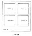
- FIG. 2illustrates an FPGA 22 that is formed by combining two FPGA tiles 20 .
- the two FPGA tiles 20work together and communicate with each other to form the larger FPGA 22 .
- FIG. 3Aillustrates an FPGA 24 that is formed by combining four FPGA tiles 20 .
- FPGA tiles 20may be combined to form a larger FPGA that is to be manufactured as its own IC or that is to be embedded into a larger IC.
- the FPGAs 22 , 24may be embedded into SOCs.
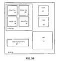
- FIG. 3Bshows an SOC 25 having the FPGA 24 embedded therein.
- the SOC 25includes several other components.
- the other componentsmay include, for example, a read only memory (ROM) 27 , a random access memory (RAM) 29 , a microprocessor 31 , and any other components 33 .
- ROMread only memory
- RAMrandom access memory
- microprocessor 31a microprocessor
- the FPGA 26includes four FPGA tiles 20 and four pad rings 28 , 30 , 32 , 34 .
- the pad rings 28 , 30 , 32 , 34are used to couple the FPGA tiles 20 to the IC package pins of the FPGA 26 .
- the global routing structure 36will be described in more detail below, but in general, it is a routing structure used to route inter-tile global signals between the FPGA tiles 20 . It should be understood that the global routing structure 36 may be included in any combination of FPGA tiles 20 , including for example the FPGAs 22 , 24 , in accordance with the present invention. Furthermore, the global routing structure 36 may be used whether the combined FPGA tiles 20 are manufactured as their own IC or embedded into a larger IC.
- the FPGA tiles that are combinedmay be identical (as are the tiles in the FPGAs 22 , 24 , 26 ), or of different sizes and designs in accordance with the present invention.
- An advantage of using identical FPGA tilesis that it provides an economical solution for providing FPGAs having sizes that are appropriate for the intended uses/applications. Such a solution is economical because only one FPGA tile needs to be designed, and then the necessary number of tiles are combined to form an FPGA.
- an “FPGA tile”is considered herein to be an FPGA. In other words, a single FPGA tile 20 can be used by itself to form an FPGA.
- the FPGA tile 20includes several functional groups (FGs) 40 that are surrounded by several interface groups (IGs) 42 .
- the FGs 40are small multifunction circuits that are capable of realizing many or all Boolean functions.
- the FGs 40include look-up tables (LUTs) and other circuits capable of realizing Boolean functions, as well as memory cells that are used to configure logic functions such as addition, subtraction, etc.
- the IGs 42are used for interfacing the FPGA tile 20 to other FPGA tiles or devices, or to pad rings for connecting the FPGA tile 20 to IC package pins.
- the logic structure of the FPGA tile 20is provided by the FGs 40 and the IGs 42 . Also included in the FPGA tile 20 , but not shown in FIG. 5 , are several horizontal and vertical regular routing buses, routing interconnect areas, switching transistors, and global routing structure, all of which will be discussed below.
- an exemplary version of the FG 40includes first set of input and output ports 44 , intra-tile global input and output ports 46 , and inter-tile global input port 48 .
- the first set of input and output portscarry input signals EUI[ 0 : 4 ] (upper input) and EBI[ 0 : 4 ] (bottom input) These inputs are the basic inputs on which the Boolean functions and logic operation of the FG 40 are performed.
- the first set of input and output ports 44also carry output signals Y[ 0 : 4 ]. These signals are the basic outputs which carry the result of the Boolean functions and logic operation of the FG 40 .
- the first set of input and output ports 44route signals that are carried within the FPGA tile 20 on horizontal and vertical regular routing buses and routing interconnect areas. If any of the signals sent via first inputs and output ports 44 are to be sent to a different FPGA tile, they are passed through an IG 42 as shown in FIG. 5 .
- the intra-tile global input and output ports 46carry input signals LGG[ 0 : 5 ] and output signal LINT.
- the LINT signalis carried via a second set of routing resources. Specifically, in some situations the first set of routing output signals Y[ 0 : 4 ] cannot be sent to the intended FG 40 because the first set of routing conductors and routing interconnect areas do not provide the necessary connections. Or, in other situations, it may be desirable not to use the system central processing unit (CPU) time to send a signal through the first set of routing conductors and routing interconnect areas. In these situations, the needed one of the regular routing output signals Y[ 0 : 4 ] can be selected as the LINT signal.
- CPUsystem central processing unit
- the LINT signalis routed around the FPGA tile 20 by a routing structure that is separate from the first set of routing conductors and routing interconnect areas used to route the first set of output signals Y[ 0 : 4 ]. Therefore, the LINT signal can be sent to any FG 40 or IG 42 regardless of whether the first set of routing conductors and routing interconnect areas provide the necessary connections.
- the LINT signalsare received by the FG 40 via input ports LGG[ 0 : 5 ] which are part of the second set of routing conductors carrying the LINT signals.
- the intra-tile global input and output ports 46carry signals that are routed within the boundaries of the FPGA tile 20 and are preferably not routed between FPGA tiles. The intra-tile global inputs and output ports 46 and the generation and use of the LINT signal will be discussed in more detail below.
- the inter-tile global input port 48carries the input signals GG[ 0 : 7 ]. These signals are sent to every FG 40 in all FPGA tiles. As will be discussed below, selected ones of the input signals GG[ 0 : 7 ] are used to control the clock/enable/preset/clear (C/E/P/C) inputs of flip-flops included in each FG 40 .
- Each FG 40also includes a CL input and a CO output.
- CL input and CO outputThe purpose of these input and output ports is to implement a carry chain for faster utilization of logic resources.
- each FG 40preferably includes four logic units (LU) 50 , 52 , 54 , 56 .
- the LUs 50 , 52 , 54 , 56provide the Boolean functions and logic operations of the FG 40 .
- Each of the LUs 50 , 52 , 54 , 56includes several inputs on which Boolean functions and logic operations are performed. As shown, each of the LUs 50 , 52 , 54 , 56 includes twenty such inputs, but it should be understood that the number of inputs may vary in accordance with the present invention.
- each of the LUs 50 , 52 , 54 , 56receives signals through input ports UI[ 0 : 4 ] and BI[ 0 : 4 ] which correspond to signals received through regular input ports EUI[ 0 : 4 ] and EBI[ 0 : 4 ] discussed above. Furthermore, each of the LUs 50 , 52 , 54 , 56 receives signals through input port GI[ 0 : 1 ].
- the input signals GI[ 0 : 1 ]are generated by the LGG selection circuit 58 which selects two of the input signals LGG[ 0 : 5 ]. As mentioned above, the input port LGG[ 0 : 5 ] carries selected ones of the signals traveling via the LINT bus.
- each of the LUs 50 , 52 , 54 , 56receives signals via input port JI[ 0 : 7 ].
- the input signals via input port JI[ 0 : 7 ]include two output signals from each of the LUs 50 , 52 , 54 , 56 .
- two output signals of each of the LUs 50 , 52 , 54 , 56are fed back to the inputs by way of JI[ 0 : 7 ].
- Each of the LUs 50 , 52 , 54 , 56also includes a clock/enable/preset/clear (C/E/P/C) input. This input is used to control a flip-flop included inside each of the LUs 50 , 52 , 54 , 56 .
- the C/E/P/C inputis generated by a C/E/P/C selection circuit 60 .
- the C/E/P/C selection circuit 60receives inputs EUI[ 0 : 4 ], EBI[ 0 : 4 ], JI[ 0 : 7 ], GI[ 0 : 1 ], and GG[ 0 : 7 ]. From these signals, the C/E/P/C selection circuit 60 selects four signals to be used as the C/E/P/C signals.
- Each of the LUs 50 , 52 , 54 , 56includes three outputs: Y, JPO, and JO. These outputs carry the result of the Boolean functions and logic operations performed by the LU.
- the JPQ and JO outputs from each of the LUs 50 , 52 , 54 , 56are grouped together to form the JI[ 0 : 7 ] bus which is fed back into the inputs of the LUs 50 , 52 , 54 , 56 .
- the Y output from each of the LUs 50 , 52 , 54 , 56are grouped together to form Y[ 0 : 3 ] of the Y[ 0 : 4 ] bus.
- the Y[ 4 ] signalis selected using a multiplexer (or selection circuit) 62 to select from the JI[ 0 : 7 ] bus.
- a multiplexer (or selection circuit) 62to select from the JI[ 0 : 7 ] bus.
- An advantage of selecting the Y[ 4 ] signal from the JI[ 0 : 7 ] busis that it adds flexibility to the device. In other words, the JO or JPO output of any of the LUs 50 , 52 , 54 , 56 can be chosen as the Y[ 4 ] signal.
- the LINT signalcan be selected to be any one of the Y[ 0 : 4 ] signals using a multiplexer 64 .
- the use of the LINT signaladds a tremendous amount of flexibility to the FPGA tile 20 because the LINT signal can be sent to any of the FGs 40 or IGs 42 . This is because the LINT signal is routed around the FPGA tile 20 using a routing structure that is separate and independent from that of the Y[ 0 : 4 ] bus.
- the multiplexer 64can be used to select that one of the Y[ 0 : 4 ] signals as the LINT signal in order to send the signal to the desired destination.
- one exemplary version of the LGG selection circuit 58includes two six-to-one multiplexers 66 , 68 .
- Each multiplexer 66 , 68selects one of the input signals LGG[ 0 : 5 ].
- the signal selected by multiplexer 66becomes the signal GI[ 0 ]
- the signal selected by multiplexer 68becomes the signal GI[ 1 ]. Because the LGG[ 0 : 5 ] bus is supplied to both multiplexers 66 , 68 , it is possible for the signals GI[ 0 ] and GI[l] to be the same signal.
- the LGG[ 0 : 5 ] busis a way for LINT signals from any FG 40 or IG 42 to be sent to any FG 40 or IG 42 .
- the exemplary version of the LGG selection circuit 58 showncan select any two of these LINT signals for sending to the LUs 50 , 52 , 54 , 56 via the GI[ 0 : 1 ] bus. It should be understood, however, that various different designs of the LGG selection circuit 58 may be used to select various different numbers of signals from the LGG[ 0 : 5 ] bus for the LUs 50 , 52 , 54 , 56 in accordance with the present invention.
- the circuit 60includes two twenty-to-one multiplexers 70 , 72 .
- Each multiplexer 70 , 72selects one signal from the buses EUI[ 0 : 4 ], EBI[ 0 : 4 ], JI[ 0 : 7 ], and GI[ 0 : 1 ].
- the signal selected by multiplexer 70becomes the signal GX[ 0 ]
- the signal selected by multiplexer 72becomes the signal GX[ 1 ].
- the bus GX[ 0 : 1 ]is supplied to the inputs of four eleven-to-one multiplexers 74 , 76 , 78 , 80 .
- the signal selected by multiplexer 74becomes the clock signal CLK
- the signal selected by multiplexer 76becomes the enable signal E
- the signal selected by multiplexer 78becomes the preset signal PRSTN
- the signal selected by multiplexer 80becomes the clear signal CLRN.
- the use of the four multiplexers 74 , 76 , 78 , 80allows any of the signals GX[ 0 : 1 ], GG[ 0 : 7 ], and ground to be selected as one of the C/E/P/C signals.
- the GG[ 0 : 7 ] busis an inter-tile global bus that is sent to every FG 40 in all FPGA tiles.
- the signals in the GG[ 0 : 7 ] busare often selected as the C/E/P/C signals.
- the C/E/P/C selection circuit 60advantageously allows the two signals GX[ 0 : 1 ] to be selected as the C/E/P/C signals.
- the two signals GX[ 0 : 1 ]can be selected from any of the buses EUI[ 0 : 4 ], EBI[ 0 : 4 ], JI[ 0 : 7 ], and GI[ 0 : 1 ].
- the C/E/P/C selection circuit 60allows numerous different signals to be selected as the C/E/P/C signals which provides for a very flexible device. It should be well understood, however, that the illustrated C/E/P/C selection circuit 60 is just one exemplary version of such a selection circuit and that various different designs of the C/E/P/C selection circuit 60 may be used to select various different signals in accordance with the present invention.
- the LUs 50 , 52 , 54 , 56are preferably all of the same design, but it should be understood that such is not required in accordance with the present invention.
- the LU 50includes two look-up tables (LUT) 82 , 84 .
- Each LUT 82 , 84includes three inputs A, B, C, an output Y, and several internal memory cells (not shown).
- the LUTs 82 , 84are configured by programming the internal memory cells, and the specific setting of the internal memory cells taken together provides a specific configuration for each of the LUTs 82 , 84 .
- the configuration data used to program the internal memory cellsis generated by design software. Once a specific configuration of the internal memory cells is decided upon, the inputs A, B, C may be used to generate the output Y in accordance with the desired logic function.
- the inputs A, B, C of the LUT 82are provided by the twenty-to-one multiplexers 86 , 88 , 90 , respectively, and the inputs A, B, C of the LUT 84 are provided by the twenty-to-one multiplexers 92 , 94 , 96 , respectively.
- Each of the multiplexers 86 , 88 , 90 , 92 , 94 , 96receives as inputs the four buses EUI[ 0 : 4 ], EBI[ 0 : 4 ], JI[ 0 : 7 ], and GI[ 0 : 1 ]. Therefore, three signals are selected from these twenty signals as the inputs A, B, C for each of the LUTs 82 , 84 .
- the LUT 82can be used by itself and the LUT 84 is not needed.
- the Y output of the LUT 82can be sent directly to the JO output of the LU 50 , or the Y output of the LUT 82 can be sent to the Y output of the LU 50 by using the two-to-one multiplexer 104 to select the Y output of the LUT 82 .
- the Y output of the LUT 82can be sent to the JPO output of the LU 50 by using the two-to-one multiplexer 98 to select the Y output of the LUT 82 and the two-to-one multiplexer 102 to select the output of the multiplexer 98 .
- the multiplexers 98 , 102 , 104can be used to send the Y output of the LUT 82 to any of the outputs Y, JO, JPO of the LU 50 .
- One purpose of including two LUTs 82 , 84 in the LU 50is so that they can be used together to provide a four-input LUT.
- the Y output of the LUT 82 and the Y output of the LUT 84are connected to the inputs of the two-to-one multiplexer 98 .
- the multiplexer 98is controlled by the twenty-to-one multiplexer 100 which receives as its inputs the four buses EUI[ 0 : 4 ], EBI[ 0 : 4 ], JI[ 0 : 7 ], and GI[ 0 : 1 ].
- the LUTs 82 , 84both receive the first, second and third inputs at their A, B, C inputs, and the multiplexer 100 is programmed to select the fourth input and provide it to the control input of the multiplexer 98 .
- the multiplexer 100is programmed to select the fourth input and provide it to the control input of the multiplexer 98 .
- connecting the three-input LUTs 82 , 84 in this mannerwill simulate a single four-input LUT with the result being generated at the output of the multiplexer 98 .
- the output of the multiplexer 98can be provided to the JPO output of the LU 50 by way of the multiplexer. 102 or to the Y output of the LU 50 by way of the multiplexers 102 , 104 .
- a flip-flop 106is preferably also included in the LU 50 . Specifically, the D input of the flip-flop 106 is connected to the output of the multiplexer 98 , and the Q output of the flip-flop 106 is connected to one of the inputs of the multiplexer 102 . The clock, enable, set and reset inputs of the flip-flop 106 are connected to the corresponding signals of the C/E/P/C bus.
- One purpose of the flip-flop 106is to store the output data of the multiplexer 98 . This data can be stored and later sent to the JPO output of the LU 50 by selecting the Q output with the multiplexer 102 .
- the stored datacan also be sent to the Y output of the LU 50 by selecting the JPO signal with the multiplexer 104 .
- the inclusion of the flip-flop 106 in the LU 50adds to the flexibility of the device in that output data of the LU 50 can be stored and used at a later time.
- the IGs 42are used for interfacing the FPGA tile 20 to other FPGA tiles or devices, or to pad rings for connecting the FPGA tile 20 to IC package pins.
- the PI[ 0 : 9 ] busis used to receive data from outside of the FPGA tile 20 and pass the data to the first set of routing conductors inside of the FPGA tile 20 via the CI[ 0 : 9 ] bus.
- the CO[ 0 : 9 ] busis used to receive data from the first set of routing conductors inside of the FPGA tile 20 and pass the data to outside of the FPGA tile 20 via the PO[ 0 : 9 ] bus.
- the IG 42Similar to the FG 40 , the IG 42 also receives LINT signals via the second set of routing conductors. Specifically, for signals coming into the FPGA tile 20 , the PI[ 0 : 9 ] bus is coupled to ten, twelve-to-one multiplexers 110 that select the signals which form the CI[ 0 : 9 ] bus. If, however, the first set of routing conductors that is coupled to the CI[ 0 : 9 ] bus is unable to route a signal to the desired location within the FPGA tile 20 , the signal can be selected as the “bLINT” signal by the twelve-to-one multiplexer 112 .
- the bLINT signalis routed by the same second set of routing conductors that is used to the route the LINT signals generated by the FGs 40 .
- the bLINT signalcan be routed along this second set of routing conductors to any of the FGs 40 and/or IGs 42 in the FPGA tile 20 .
- Thisprovides a way to route any of the incoming signals PI[ 0 : 9 ] to any destination within the FPGA tile 20 even if the first set of routing conductors carrying the CI[ 0 : 9 ] bus does not provide a path to that destination.
- the CO[ 0 : 9 ] busis coupled to ten, twelve-to-one multiplexers 114 that select the signals which form the PO[ 0 : 9 ] bus. If, however, the first set of routing conductors that are coupled to the PO[ 0 : 9 ] bus are unable to route a signal to the desired location outside of the FPGA tile 20 (e.g., in a neighboring FPGA tile), the signal can be selected as the “tLINT” signal by the twelve-to-one multiplexer 116 .
- the tLINT signalis routed by a second set of routine conductors that is used to route the signals from a second output port LINT in the neighboring FPGA tile, and as such, the tLINT signal can be routed to any of the FGs and/or IGs in the neighboring FPGA tile. This provides a way to route any of the outgoing signals CO[ 0 : 9 ] to any destination within the neighboring FPGA tile even if the first set of routing conductors carrying the PO[ 0 : 9 ] bus does not provide a path to that destination.
- the second set of routing conductors within the FPGA tile 20 that carries LINT signalsincludes the LGG[ 0 : 5 ]) bus. Specifically, several LINT signals that need to be routed around the FPGA tile 20 are grouped together and travel via the LGG[ 0 : 5 ] bus.
- the LGG[ 0 : 5 ] busis provided to every FG 40 and IG 42 so that LINT signals can be sent to every device.
- the IGs 42receive the LGG[ 0 : 5 ] bus from inside of the FPGA tile 20 at input bLGG[ 0 : 5 ].
- the bLGG[ 0 : 5 ] inputis coupled to the six-to-one multiplexers 118 , 120 , which have their outputs coupled to the multiplexers 114 , 116 .
- any LINT signal generated within the FPGA tile 20can be sent outside of the FPGA tile 20 on the PO[ 0 : 9 ] bus or as the tLINT signal by programming the appropriate multiplexers 114 , 116 to select the outputs of the appropriate multiplexers 118 , 120 .
- an LGG bus in a neighboring FPGA tilecan be connected to the tLGG[ 0 : 5 ] input of the IG 42 .
- the tLGG[ 0 : 5 ] inputis coupled to the six-to-one multiplexers 122 , 124 , which have their outputs coupled to the multiplexers 110 , 112 .
- any LINT signal generated outside of the FPGA tile 20can be sent inside the FPGA tile 20 on the CI[ 0 : 9 ] bus or as the bLINT signal by programming the appropriate multiplexers 110 , 112 to select the outputs of the appropriate multiplexers 122 , 124 .
- FIG. 12shows an alternative IG 42 ′ having no tLINT or tLGG[ 0 : 5 ] inputs.
- FIG. 12shows an alternative IG 42 ′ having no tLINT or tLGG[ 0 : 5 ] inputs.
- the PO[ 0 : 9 ] outputs and the PI[ 0 : 9 ] inputswill be coupled through the pad ring to the IC package I/Os (i.e., the IC package input/output pins).
- the PI[ 0 : 9 ] busis coupled to several I/Os 101 , 103 , 105 , 107 , 109 .
- the multiplexers 116 , 122 , 124are eliminated, and the multiplexers 110 , 112 are replaced with ten-to-one multiplexers 126 , 128 .
- FIG. 12also illustrates another important feature of the present invention. Specifically, in the scenario where a side of the FPGA tile 20 is to be coupled to a pad ring for I/O purposes, the I/Os 101 , 103 , 105 , 107 , 109 may be directly coupled to the IG 42 ′. Furthermore, the I/Os 101 , 103 , 105 , 107 , 109 may be directly coupled to the multiplexers 126 , 128 . In other words, the I/Os 101 , 103 , 105 , 107 , 109 can be directly coupled to the multiplexers 126 , 128 without first connecting to a routing channel.
- connection to a routing channelis made after the IG 42 ′ and multiplexers 126 , 128 .
- I/Osare directly coupled to the multiplexers 126 , 128 and then go on to the routing channel or other routing resources.
- the IGs of two neighboring FPGA tilesmay be combined into one IG in accordance with the present invention.
- the PO[ 0 : 9 ], PI[ 0 : 9 ], tLGG[ 0 : 5 ] buses and the tLINT output portwill typically not be coupled to a separate IG of a neighboring tile, but rather, these input and output ports will be coupled into the routing structures of the neighboring FPGA tile and the IG 42 will also serve as the IG of the neighboring tile.
- any of the multiplexers (selection circuits) discussed hereinmay comprise any of the selection circuits described in copending U.S. patent application Ser. No. 09/250,781, filed Feb. 12, 1999, entitled “MULTI-DIMENSIONAL PROGRAMMABLE INPUT SELECTION APPARATUS AND METHOD”, invented by Chung-yuan Sun, and commonly assigned herewith, the full disclosure of which is hereby incorporated into the present application by reference.
- FIG. 13there is illustrated a more detailed diagram showing approximately one-quarter of an exemplary version of the FPGA tile 20 .
- the portion of the FPGA tile 20 that is illustratedis designated by 129 in FIG. 5 . It will be appreciated by those of ordinary skill in the art that the remaining portions of the FPGA tile 20 are mirror images of the illustrated portion 129 .
- FIG. 13illustrates the first set of routing conductors of the FPGA tile 20 that is used to route signals via input and output ports 44 of the FGs 40 .
- the input and output ports 44carry the signals to first input ports EUI[ 0 : 4 ], EBI[ 0 : 4 ], and the signals from first output ports Y[ 0 : 4 ].
- the first set of routing conductors of the FPGA tile 20also handles routing of the CO[ 0 : 9 ] and CI[ 0 : 9 ] buses to and from the IGs 42 .
- the first set of routing conductors of the FPGA tile 20includes first horizontal routing buses 150 , 152 , 154 , 156 and several vertical regular routing buses 158 , 160 , 162 .
- the horizontal routing buses 150 , 152 , 154 , 156may each include X number of lines
- the horizontal routing bus 164may include A number of lines
- the vertical routing buses 160 , 162may each include Y number of lines
- the vertical routing bus 158may include B number of lines.
- the horizontal routing buses 150 , 152 , 154 , 156may each include 50 lines
- the horizontal routing bus 164may include 70 lines
- the vertical routing buses 160 , 162may each include 60 lines
- the vertical routing bus 158may include 70 lines.
- routing interconnect areas 130 , 132 , 134 , 136 , 138 , 140 , 142 , 144 , 146 , 148are included in the FPGA tile 20 .
- the routing interconnect areas 130 , 138 , 144 , 146are used to transfer data from one of the vertical routing buses to one of the horizontal routing buses.
- the other routing interconnect areas 132 , 134 , 136 , 140 , 142 , 148are used to transfer data to or from one of the IGs 42 or one of the FGs 40 to or from one of the vertical routing buses or one of the horizontal routing buses.
- the routing buses and the routing interconnect areasform the regular routing structure of the FPGA tile 20 .
- FIG. 14illustrates an exemplary structure for the routing interconnect areas 130 , 132 , 134 .
- the horizontal routing bus 152includes 50 lines and the vertical routing bus 160 includes 60 lines. It should be well understood, however, that the specific number of lines in any of the routing buses may vary in accordance with the present invention.
- any of the signal busessuch as for example EUI[ 0 : 4 ], EBI[ 0 : 4 ], Y[ 0 : 4 ], LGG[ 0 : 5 ], GG[ 0 : 7 ], JI[ 0 : 7 ], GI[ 0 : 1 ], CO[ 0 : 9 ], CI[ 0 : 9 ], PO[ 0 : 9 ], PI[ 0 : 9 ], may vary in accordance with the present invention.
- Each of the routing interconnect areas 130 , 132 , 134includes several transistor switches and corresponding memory cells which are used for making the connections between the various buses.
- Each transistor switch and memory cellis illustrated in the figure as a circle (or bubble) drawn at the intersection of signal lines to be coupled together.
- FIG. 15shows a detail of the circles designated by 170 .
- the circles 172 , 174 , 176 , 178 , 180includes transistor switches M 2 , M 4 , M 6 , M 8 , M 10 , respectively.
- Each of the transistor switches M 2 , M 4 , M 6 , M 8 , M 10has its source and drain coupled to intersecting signal lines and its gate coupled to a corresponding memory cell 182 , 184 , 186 , 188 , 190 .
- Each of the memory cellsstores one bit of configuration data to control whether or not its corresponding transistor switch is turned on or off. When a transistor switch is turned on, the lines to which it is connected are coupled together.
- One of the FGs 40 and its nearby routing interconnect areas 130 , 132 , 134are illustrated.
- the Y[ 0 : 4 ] output port of the FG 40is coupled to the routing interconnect area 134
- the EBI[ 0 : 4 ] input port of the FG 40is coupled to the routing interconnect area 132 .
- the FG 40outputs data onto the Y[ 0 : 4 ] bus and the routing interconnect area 134 is used to transfer that data onto bus 160 . This is done by turning on the transistor switch inside the illustrated circle (or bubble) at the appropriate intersection of signal lines.
- Each transistor switchis turned on by programming its corresponding memory cell.
- the routing interconnect area 132is used to transfer data from bus 152 onto the EBI[ 0 : 4 ] bus of the FG 40 . Again, this is accomplished by programming the memory cell to turn on the transistor switch at the appropriate intersection.
- the routing interconnect area 130is used to transfer data from bus 160 onto bus 152 , again by programming the memory cell to turn on the transistor switch at the appropriate intersection.
- the routing interconnect areas 130 , 132 , 134include transistor switches and memory cells at many intersections of signal lines, but not at all intersections. (Again, the transistor switches and memory cells are inside the illustrated circles or bubbles). When a transistor switch and memory cell is included at every intersection of signal lines, this is known as a “fully populated” routing interconnect portion. A fully populated routing interconnect portion is shown in the routing interconnect area 132 at 192 . It should be well understood that the specific intersections chosen to have a transistor switch and memory cell, and which areas are fully populated (if any), may vary widely in accordance with the present invention. In other words, many different patterns of transistor switches and memory cells may be used in the routing interconnect areas 130 , 132 , 134 in accordance with the present invention.
- the other routing interconnect areas 136 , 138 , 140 , 142 , 144 , 146 , 148 in the FPGA tile 20are similar to the routing interconnect areas 130 , 132 , 134 . Some, however, will have different numbers of signal lines and intersections. For example, the routing interconnect areas 136 , 144 may have a greater number of signal lines in the horizontal bus 164 due in part to ten signals (instead of five) being transferred to the CO[ 0 : 9 ] bus of the IGs 42 . Similarly, the routing interconnect areas 146 , 148 will have fewer inputs and/or outputs because they are located at the end of a row.
- the number of transistor switches used and their positioning in the FPGA tile 20can change in accordance with the present invention.
- the specific arrangement and positioning of IGs, FGs, routing buses, routing interconnect areas, and switching transistors within routing interconnect areaswill vary greatly depending on the particular application. It should be understood that the configurations illustrated in the figures herein are example configurations.
- FIGS. 16A and 16Billustrate the second set of routing conductors of the FPGA tile 20 .
- the second set of routing conductorsis separate from the first set of routing conductors and routing interconnect areas used to route the output signals Y[ 0 : 4 ].
- the second set of routing conductorsis used for routing signals via input and output ports 46 which include input port LGG[ 0 : 5 ] and output port LINT.
- the LINT routing structureis a second set of routing conductors that can be used to send a signal in situations when the first set of routing conductors cannot be used to send a signal to the intended destination.
- the signalcan be sent to any of the FGs 40 and/or IGs 42 by selecting the needed one of the output signals Y[ 0 : 4 ] as the LINT signal as described above and sending it over the second set of routing conductors.
- the signals sent via the LINT output port of six devicesare assembled to form the LGG[ 0 : 5 ] bus. While the LGG[ 0 : 5 ] bus is illustrated as a six-signal bus, it should be well understood that the number of signals in the LGG bus may vary in accordance with the present invention. Furthermore, the LGG bus is made up of LINT signals from the FGs 40 and bLINT signals from the IGs 42 . As discussed above, the “b” designation on the bLINT signals of the IGs 42 indicates that these signals are internal to the FPGA tile 20 as opposed to the external tLINT signals. Therefore, when discussing the formation of the LGG[ 0 : 5 ] bus, use of the term “LINT” will generally be intended to cover both the LINT signal generated by the FGs 40 and the bLINT signal generated by the IGs 42 .
- the LGG[ 0 : 5 ] busis assembled as follows.
- the first column of IGs 42has their bLINT outputs coupled to an eight-signal bus 200 .
- Six, eight-to-one multiplexers 202are coupled to bus 200 .
- the output of each of the multiplexers 202is coupled to a corresponding tri-state buffer 204 .
- the outputs of the tri-state buffers 204are coupled to the LGG[ 0 : 5 ] bus.
- the LINT output of each FG 40 and the bLINT output of each IG 42are coupled to a ten-signal bus 206 .
- Six, ten-to-one multiplexers 208are coupled to bus 206 .
- the output of each of the multiplexers 208is coupled to a corresponding tri-state buffer 204 , which in turn are coupled to the LGG[ 0 : 5 ] bus.
- the last column of IGs 42has their bLINT outputs coupled to an eight-signal bus 210 .
- Six, eight-to-one multiplexers 202 and tri-state buffers 204couple bus 210 to the LGG[ 0 : 5 ] bus.
- the LINT output of each FG 40 and the bLINT output of each IG 42are coupled to a ten-signal bus 212 , which in turn is coupled to the LGG[ 0 : 5 ] bus via six, ten-to-one multiplexers 208 and tri-state buffers 204 .
- the rest of the FGs 40 and IGs 42 in the FPGA tile 20that are not shown in FIGS. 16A and 16B are connected to the LGG[ 0 : 5 ] 0 bus in a similar manner.
- each of the multiplexers 202 , 208selects a LINT signal from its input bus, that is, the respective one of buses 200 , 206 , 210 , 212 . Up to six of these selected LINT signals may be placed onto the LGG[ 0 : 5 ] bus. This is done by placing six of the tri-state buffers 204 into a conducting state and placing the remaining tri-state buffers into a non-conducting state. The six tri-state buffers 204 that are placed into a conducting state should correspond to the multiplexers 202 , 208 that have selected the desired LINT signals.
- the LGG[ 0 : 5 ] busis routed to all of the FGs 40 and IGs 42 in the FPGA tile 20 . In this way, a LINT signal from any of the FGs 40 and IGs 42 can be sent to any of the FGs 40 and IGs 42 , independent of the first set of routing conductors used for the Y[ 0 : 4 ] bus.
- FIGS. 16A and 16Balso show the routing of the GG[ 0 : 7 ] bus.
- the GG[ 0 : 7 ] busforms the inter-tile global signals 48 . These signals are sent to every FG 40 in all FPGA tiles.
- the GG[ 0 : 7 ] busextends through the border of the FPGA tile 20 as indicated at 214 so that it can go to other FPGA tiles.
- the GG[ 0 : 7 ] busextends through the border of the FPGA tile 20 without going through an IG 42 .
- selected ones of the input signals GG[ 0 : 7 ]may be used to control the clock/enable/preset/clear (C/E/P/C) inputs of flip-flops included in each FG 40 .
- the GG[ 0 : 7 ] busmay include more or fewer signals in accordance with the present invention.
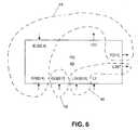
- the global signal routing structure 36is illustrated in more detail. As mentioned above, the global signal routing structure 36 is used to route inter-tile global signals between the FPGA tiles 20 .
- the GG[ 0 : 7 ] bus(which forms the inter-tile global signals 48 ) is included in the global signal routing structure 36 and is shown connecting to all four FPGA tiles 20 .
- the GG[ 0 : 7 ] buscan be coupled to inputs 220 , 222 to send signals that are to be sent on the GG[ 0 : 7 ] bus. Selected ones of the inputs 220 , 222 can be coupled to selected signals of the GG[ 0 : 7 ] bus by means of transistor switches and memory cells (such as is described above), examples of which are indicated by circles 224 , 226 .
- the global signal routing structure 36also includes bus 230 to connect to the pad ring.
- FIG. 18illustrates another option for coupling two FPGA tiles 20 together.
- an intermediate routing track 240may be used.
- the output PO[ 0 : 9 ] bus of the IG 42 of one tile 20is coupled to the track 240
- the input PI[ 0 : 9 ] bus of the IG 42 of the other tile 20is coupled to the track 240 at a different location.
- connections to the track 240may be by way of hard wired connections for by way of transistor switches and memory cells as described above. The later would, of course, be programmable. It should be understood that the use of the intermediate routing track 240 is optional.
- FIG. 19shows the LINT signal distribution through a fixed network.
- the LINT signalis sent via a second set of routing conductors that can be used to send a signal in situations when the first set of routing conductors Y[ 0 : 4 ] cannot be used to send a signal to the intended destination. This may occur because a transistor switch and memory cell may not have been placed at the needed intersection of signal lines in one or more of the regular routing interconnect areas 130 , 132 , 134 , 136 , 138 , 140 , 142 , 144 , 146 , 148 .
- the signalcan be sent to any of the FGs 40 and/or IGs 42 by selecting the needed one of the regular routing output signals Y[ 0 : 4 ] as the LINT signal as described above and sending it over the second set of routing conductors.
- FIGS. 20 and 21show yet another embodiment of the present invention.
- a third routing structureis added to FPGA tile 20 making FPGA tile 20 extremely flexible and enabling signals to be sent to or from any FG or IG 42 .
- FIGS. 20 and 21show the SLINT signal distribution through a flexible network.
- the SLINT networkis a third set of routing conductors that can be used to send a signal in situations when the first set of routing conductors 44 cannot be used to send a signal to the intended destination.
- the SLINT networkis an extension of the LINT concept except that the SLINT network employs flexible routing resources with tracks and switches. Every output of an FG 40 Y[ 0 : 4 ] can be used to drive the SLINT network.
- every output of an IG 42 PI[ 0 : 9 ]can be used to drive the SLINT network.
- a signalwill be selectively placed in the SLINT network if the first set of routing conductors cannot be used to send a signal. This may occur because a transistor switch and memory cell may not have been placed at the needed intersection of signal lines in one or more of the first set of routing conductors interconnect areas 130 , 132 , 134 , 136 , 138 , 140 , 142 , 144 , 146 , 148 .
- signalstravel through a special Set of tracks, SLVT 248 , SLHT 250 and SLIT 252 before reaching the third input ports of FGs 40 , namely SL[ 0 : 4 ] 254 via input track SLIT [ 0 : 4 ].
- FIG. 21illustrates an exemplary structure for the routing interconnect areas 256 , 258 , 260 and 262 between adjacent FGs. It should be well understood, however, that the specific number of lines in any of the routing buses may vary in accordance with the present invention. Furthermore, from this disclosure, it will be apparent to persons of ordinary skill in the art that the specific number of lines in any of the signal buses, such as for example Y[ 0 : 4 ], SL[ 0 : 4 ], may vary in accordance with the present invention.
- each of the third set of routing conductors interconnect areas 256 , 258 , 260 , 262includes several transistor switches and corresponding memory cells which are used for making the connections between the various buses.
- Each transistor switch and memory cellis illustrated in the figure as a circle (or bubble) drawn at the intersection of signal lines to be coupled together. In order to illustrate this, FIG. 15 shows a detail of the circles designated by 170 .
- the third set of routing conductors interconnect areas 256 , 258 , 260 , 262includes transistor switches and memory cells at many intersections of signal lines, but not at all intersections. (Again, the transistor switches and memory cells are inside the illustrated circles or bubbles). When a transistor switch and memory cell is included at every intersection of signal lines, this is known as a “fully populated” routing interconnect portion. A fully populated routing interconnect portion is shown in the routing interconnect area 258 . It should be well understood that the specific intersections chosen to have a transistor switch and memory cell, and which areas are fully populated (if any), may vary widely in accordance with the present invention. In other words, many different patterns of transistor switches and memory cells may be used in the routing interconnect areas 256 , 258 , 260 , 262 in accordance with the present invention.
- the number of transistor switches used and their positioning in the FPGA tile 20can change in accordance with the present invention.
- the specific arrangement and positioning of IGs, FGs, routing buses, routing interconnect areas, and switching transistors within routing interconnect areaswill vary greatly depending on the particular application. From this disclosure, it will be apparent to persons of ordinary skill in the art that the configurations illustrated in the figures herein are example configurations.
- FIGS. 22 and 23show the SLINT signal distribution through a flexible network as it pertains to IGs 42 .
- FIGS. 22 and 23illustrate an exemplary structure for the third set of routing conductors interconnect areas 264 , 266 , 268 and 270 between adjacent top/bottom IGs 42 and left/right IGs 42 . Every output of an IG 40 , PI[ 0 : 9 ] can be used to drive the SLINT network.
- the routing interconnect areas 264 , 266 , 268 , 270includes transistor switches and memory cells at many intersections of signal lines, but not at all intersections. From this disclosure, it will be apparent to persons of ordinary skill in the art, however, that the specific number of lines in any of the routing buses may vary in accordance with the present invention. Furthermore, it should be well understood that the specific number of lines in any of the signal buses, such as for example PI[ 0 : 9 ], SL[ 0 : 3 ], may vary in accordance with the present invention.
- FIG. 24discloses a method of routing a FPGA.
- a method of routing an FPGA in accordance with the present inventionbegins at input block 300 .
- a userinputs a function netlist that defines a user circuit.
- the user circuitwill define the programmable connections to be programmed to implement the desired user function.
- These programmable connectionsinclude programmable interconnections of the FPGA array, as well as the connections within internal components included within the FPGA.
- Internal componentsare defined as, for example, configurable functional groups, interface groups, selection circuits, multiplexer circuits, memory cells, look up tables, PLA blocks, non-volatile blocks, DRAM blocks, ROM blocks, RAM, FIFO, PLL, DLL, FLASH memory. multipliers, DSP cores, MPU cores, DAC, ADC, and any other internal components as known by those skilled in the art.
- Programming the FPGAcauses not only the programmable interconnections of the FPGA to be configured, but also causes the connections within the internal components included within the FPGA to be connected which ultimately results in lines being coupled together or not being coupled together, due to transistors being turned on and off.
- the user circuitis optimized.
- the user cells defining the optimized user circuitare placed in the FPGA.
- the circuitis routed.
- the third set of routing conductorsare employed in addition to the first set of routing conductors and are used only when the routing requirements cannot be met with first set of routing conductors.
- the bitstreamis generated.
- the FPGAis programmed with the user circuit.
Landscapes
- Engineering & Computer Science (AREA)
- Physics & Mathematics (AREA)
- Computer Hardware Design (AREA)
- General Engineering & Computer Science (AREA)
- Theoretical Computer Science (AREA)
- Mathematical Physics (AREA)
- Evolutionary Computation (AREA)
- Geometry (AREA)
- General Physics & Mathematics (AREA)
- Computing Systems (AREA)
- Computer Networks & Wireless Communication (AREA)
- Design And Manufacture Of Integrated Circuits (AREA)
- Logic Circuits (AREA)
Abstract
Description
Claims (14)
Priority Applications (5)
| Application Number | Priority Date | Filing Date | Title |
|---|---|---|---|
| US10/429,002US6888375B2 (en) | 2000-09-02 | 2003-04-30 | Tileable field-programmable gate array architecture |
| US11/056,957US7015719B1 (en) | 2000-09-02 | 2005-02-11 | Tileable field-programmable gate array architecture |
| US11/335,396US7157938B2 (en) | 2000-09-02 | 2006-01-18 | Tileable field-programmable gate array architecture |
| US11/561,705US7342416B2 (en) | 2000-09-02 | 2006-11-20 | Tileable field-programmable gate array architecture |
| US12/036,470US20080238477A1 (en) | 2000-09-02 | 2008-02-25 | Tileable field-programmable gate array architecture |
Applications Claiming Priority (3)
| Application Number | Priority Date | Filing Date | Title |
|---|---|---|---|
| US09/654,240US6476636B1 (en) | 2000-09-02 | 2000-09-02 | Tileable field-programmable gate array architecture |
| US10/066,398US6700404B1 (en) | 2000-09-02 | 2002-01-30 | Tileable field-programmable gate array architecture |
| US10/429,002US6888375B2 (en) | 2000-09-02 | 2003-04-30 | Tileable field-programmable gate array architecture |
Related Parent Applications (1)
| Application Number | Title | Priority Date | Filing Date |
|---|---|---|---|
| US10/066,398ContinuationUS6700404B1 (en) | 2000-09-02 | 2002-01-30 | Tileable field-programmable gate array architecture |
Related Child Applications (1)
| Application Number | Title | Priority Date | Filing Date |
|---|---|---|---|
| US11/056,957ContinuationUS7015719B1 (en) | 2000-09-02 | 2005-02-11 | Tileable field-programmable gate array architecture |
Publications (2)
| Publication Number | Publication Date |
|---|---|
| US20030218479A1 US20030218479A1 (en) | 2003-11-27 |
| US6888375B2true US6888375B2 (en) | 2005-05-03 |
Family
ID=24624042
Family Applications (11)
| Application Number | Title | Priority Date | Filing Date |
|---|---|---|---|
| US09/654,240Expired - Fee RelatedUS6476636B1 (en) | 2000-09-02 | 2000-09-02 | Tileable field-programmable gate array architecture |
| US10/066,398Expired - LifetimeUS6700404B1 (en) | 2000-09-02 | 2002-01-30 | Tileable field-programmable gate array architecture |
| US10/061,951Expired - LifetimeUS6744278B1 (en) | 2000-09-02 | 2002-01-31 | Tileable field-programmable gate array architecture |
| US10/061,955Expired - Fee RelatedUS6611153B1 (en) | 2000-09-02 | 2002-01-31 | Tileable field-programmable gate array architecture |
| US10/071,262Expired - LifetimeUS6968487B1 (en) | 2000-09-02 | 2002-02-07 | User available body scan chain |
| US10/077,190Expired - LifetimeUS6731133B1 (en) | 2000-09-02 | 2002-02-15 | Routing structures for a tileable field-programmable gate array architecture |
| US10/077,188Expired - LifetimeUS6531891B1 (en) | 2000-09-02 | 2002-02-15 | Method and apparatus of memory clearing with monitoring memory cells |
| US10/077,189Expired - Fee RelatedUS7137095B1 (en) | 2000-09-02 | 2002-02-15 | Freeway routing system for a gate array |
| US10/429,002Expired - LifetimeUS6888375B2 (en) | 2000-09-02 | 2003-04-30 | Tileable field-programmable gate array architecture |
| US11/557,717AbandonedUS20070089082A1 (en) | 2000-09-02 | 2006-11-08 | Freeway routing system for a gate array |
| US12/036,470AbandonedUS20080238477A1 (en) | 2000-09-02 | 2008-02-25 | Tileable field-programmable gate array architecture |
Family Applications Before (8)
| Application Number | Title | Priority Date | Filing Date |
|---|---|---|---|
| US09/654,240Expired - Fee RelatedUS6476636B1 (en) | 2000-09-02 | 2000-09-02 | Tileable field-programmable gate array architecture |
| US10/066,398Expired - LifetimeUS6700404B1 (en) | 2000-09-02 | 2002-01-30 | Tileable field-programmable gate array architecture |
| US10/061,951Expired - LifetimeUS6744278B1 (en) | 2000-09-02 | 2002-01-31 | Tileable field-programmable gate array architecture |
| US10/061,955Expired - Fee RelatedUS6611153B1 (en) | 2000-09-02 | 2002-01-31 | Tileable field-programmable gate array architecture |
| US10/071,262Expired - LifetimeUS6968487B1 (en) | 2000-09-02 | 2002-02-07 | User available body scan chain |
| US10/077,190Expired - LifetimeUS6731133B1 (en) | 2000-09-02 | 2002-02-15 | Routing structures for a tileable field-programmable gate array architecture |
| US10/077,188Expired - LifetimeUS6531891B1 (en) | 2000-09-02 | 2002-02-15 | Method and apparatus of memory clearing with monitoring memory cells |
| US10/077,189Expired - Fee RelatedUS7137095B1 (en) | 2000-09-02 | 2002-02-15 | Freeway routing system for a gate array |
Family Applications After (2)
| Application Number | Title | Priority Date | Filing Date |
|---|---|---|---|
| US11/557,717AbandonedUS20070089082A1 (en) | 2000-09-02 | 2006-11-08 | Freeway routing system for a gate array |
| US12/036,470AbandonedUS20080238477A1 (en) | 2000-09-02 | 2008-02-25 | Tileable field-programmable gate array architecture |
Country Status (6)
| Country | Link |
|---|---|
| US (11) | US6476636B1 (en) |
| EP (1) | EP1354404B1 (en) |
| JP (1) | JP2004524715A (en) |
| AU (1) | AU2001286979A1 (en) |
| DE (1) | DE60128960T2 (en) |
| WO (1) | WO2002021694A2 (en) |
Cited By (225)
| Publication number | Priority date | Publication date | Assignee | Title |
|---|---|---|---|---|
| US7015719B1 (en)* | 2000-09-02 | 2006-03-21 | Actel Corporation | Tileable field-programmable gate array architecture |
| US20080238477A1 (en)* | 2000-09-02 | 2008-10-02 | Actel Corporation | Tileable field-programmable gate array architecture |
| US7774579B1 (en)* | 2006-04-14 | 2010-08-10 | Tilera Corporation | Protection in a parallel processing environment using access information associated with each switch to prevent data from being forwarded outside a plurality of tiles |
| US7788623B1 (en)* | 2007-11-29 | 2010-08-31 | Lattice Semiconductor Corporation | Composite wire indexing for programmable logic devices |
| US8163581B1 (en) | 2010-10-13 | 2012-04-24 | Monolith IC 3D | Semiconductor and optoelectronic devices |
| US8203148B2 (en) | 2010-10-11 | 2012-06-19 | Monolithic 3D Inc. | Semiconductor device and structure |
| US8237228B2 (en) | 2009-10-12 | 2012-08-07 | Monolithic 3D Inc. | System comprising a semiconductor device and structure |
| US8258810B2 (en) | 2010-09-30 | 2012-09-04 | Monolithic 3D Inc. | 3D semiconductor device |
| US8273610B2 (en) | 2010-11-18 | 2012-09-25 | Monolithic 3D Inc. | Method of constructing a semiconductor device and structure |
| US8283215B2 (en) | 2010-10-13 | 2012-10-09 | Monolithic 3D Inc. | Semiconductor and optoelectronic devices |
| US8294159B2 (en) | 2009-10-12 | 2012-10-23 | Monolithic 3D Inc. | Method for fabrication of a semiconductor device and structure |
| US8298875B1 (en) | 2011-03-06 | 2012-10-30 | Monolithic 3D Inc. | Method for fabrication of a semiconductor device and structure |
| US8362800B2 (en) | 2010-10-13 | 2013-01-29 | Monolithic 3D Inc. | 3D semiconductor device including field repairable logics |
| US8362482B2 (en) | 2009-04-14 | 2013-01-29 | Monolithic 3D Inc. | Semiconductor device and structure |
| US8373230B1 (en) | 2010-10-13 | 2013-02-12 | Monolithic 3D Inc. | Method for fabrication of a semiconductor device and structure |
| US8373439B2 (en) | 2009-04-14 | 2013-02-12 | Monolithic 3D Inc. | 3D semiconductor device |
| US8379458B1 (en) | 2010-10-13 | 2013-02-19 | Monolithic 3D Inc. | Semiconductor device and structure |
| US8378494B2 (en) | 2009-04-14 | 2013-02-19 | Monolithic 3D Inc. | Method for fabrication of a semiconductor device and structure |
| US8378715B2 (en) | 2009-04-14 | 2013-02-19 | Monolithic 3D Inc. | Method to construct systems |
| US8384426B2 (en) | 2009-04-14 | 2013-02-26 | Monolithic 3D Inc. | Semiconductor device and structure |
| US8405420B2 (en) | 2009-04-14 | 2013-03-26 | Monolithic 3D Inc. | System comprising a semiconductor device and structure |
| US8427200B2 (en) | 2009-04-14 | 2013-04-23 | Monolithic 3D Inc. | 3D semiconductor device |
| US8440542B2 (en) | 2010-10-11 | 2013-05-14 | Monolithic 3D Inc. | Semiconductor device and structure |
| US8450804B2 (en) | 2011-03-06 | 2013-05-28 | Monolithic 3D Inc. | Semiconductor device and structure for heat removal |
| US8461035B1 (en) | 2010-09-30 | 2013-06-11 | Monolithic 3D Inc. | Method for fabrication of a semiconductor device and structure |
| US8476145B2 (en) | 2010-10-13 | 2013-07-02 | Monolithic 3D Inc. | Method of fabricating a semiconductor device and structure |
| US8492886B2 (en) | 2010-02-16 | 2013-07-23 | Monolithic 3D Inc | 3D integrated circuit with logic |
| US8536023B2 (en) | 2010-11-22 | 2013-09-17 | Monolithic 3D Inc. | Method of manufacturing a semiconductor device and structure |
| US8541819B1 (en) | 2010-12-09 | 2013-09-24 | Monolithic 3D Inc. | Semiconductor device and structure |
| US8557632B1 (en) | 2012-04-09 | 2013-10-15 | Monolithic 3D Inc. | Method for fabrication of a semiconductor device and structure |
| US8574929B1 (en) | 2012-11-16 | 2013-11-05 | Monolithic 3D Inc. | Method to form a 3D semiconductor device and structure |
| US8581349B1 (en) | 2011-05-02 | 2013-11-12 | Monolithic 3D Inc. | 3D memory semiconductor device and structure |
| US8642416B2 (en) | 2010-07-30 | 2014-02-04 | Monolithic 3D Inc. | Method of forming three dimensional integrated circuit devices using layer transfer technique |
| US8669778B1 (en) | 2009-04-14 | 2014-03-11 | Monolithic 3D Inc. | Method for design and manufacturing of a 3D semiconductor device |
| US8674470B1 (en) | 2012-12-22 | 2014-03-18 | Monolithic 3D Inc. | Semiconductor device and structure |
| US8686428B1 (en) | 2012-11-16 | 2014-04-01 | Monolithic 3D Inc. | Semiconductor device and structure |
| US8687399B2 (en) | 2011-10-02 | 2014-04-01 | Monolithic 3D Inc. | Semiconductor device and structure |
| US8709880B2 (en) | 2010-07-30 | 2014-04-29 | Monolithic 3D Inc | Method for fabrication of a semiconductor device and structure |
| US8742476B1 (en) | 2012-11-27 | 2014-06-03 | Monolithic 3D Inc. | Semiconductor device and structure |
| US8754533B2 (en) | 2009-04-14 | 2014-06-17 | Monolithic 3D Inc. | Monolithic three-dimensional semiconductor device and structure |
| US8803206B1 (en) | 2012-12-29 | 2014-08-12 | Monolithic 3D Inc. | 3D semiconductor device and structure |
| US8901613B2 (en) | 2011-03-06 | 2014-12-02 | Monolithic 3D Inc. | Semiconductor device and structure for heat removal |
| US8902663B1 (en) | 2013-03-11 | 2014-12-02 | Monolithic 3D Inc. | Method of maintaining a memory state |
| US8975670B2 (en) | 2011-03-06 | 2015-03-10 | Monolithic 3D Inc. | Semiconductor device and structure for heat removal |
| US8994404B1 (en) | 2013-03-12 | 2015-03-31 | Monolithic 3D Inc. | Semiconductor device and structure |
| US9000557B2 (en) | 2012-03-17 | 2015-04-07 | Zvi Or-Bach | Semiconductor device and structure |
| US9029173B2 (en) | 2011-10-18 | 2015-05-12 | Monolithic 3D Inc. | Method for fabrication of a semiconductor device and structure |
| US9099424B1 (en) | 2012-08-10 | 2015-08-04 | Monolithic 3D Inc. | Semiconductor system, device and structure with heat removal |
| US9099526B2 (en) | 2010-02-16 | 2015-08-04 | Monolithic 3D Inc. | Integrated circuit device and structure |
| US9117749B1 (en) | 2013-03-15 | 2015-08-25 | Monolithic 3D Inc. | Semiconductor device and structure |
| US9197804B1 (en) | 2011-10-14 | 2015-11-24 | Monolithic 3D Inc. | Semiconductor and optoelectronic devices |
| US9219005B2 (en) | 2011-06-28 | 2015-12-22 | Monolithic 3D Inc. | Semiconductor system and device |
| US9509313B2 (en) | 2009-04-14 | 2016-11-29 | Monolithic 3D Inc. | 3D semiconductor device |
| US9577642B2 (en) | 2009-04-14 | 2017-02-21 | Monolithic 3D Inc. | Method to form a 3D semiconductor device |
| US9711407B2 (en) | 2009-04-14 | 2017-07-18 | Monolithic 3D Inc. | Method of manufacturing a three dimensional integrated circuit by transfer of a mono-crystalline layer |
| US9871034B1 (en) | 2012-12-29 | 2018-01-16 | Monolithic 3D Inc. | Semiconductor device and structure |
| US9953925B2 (en) | 2011-06-28 | 2018-04-24 | Monolithic 3D Inc. | Semiconductor system and device |
| US10043781B2 (en) | 2009-10-12 | 2018-08-07 | Monolithic 3D Inc. | 3D semiconductor device and structure |
| US10115663B2 (en) | 2012-12-29 | 2018-10-30 | Monolithic 3D Inc. | 3D semiconductor device and structure |
| US10127344B2 (en) | 2013-04-15 | 2018-11-13 | Monolithic 3D Inc. | Automation for monolithic 3D devices |
| US10157909B2 (en) | 2009-10-12 | 2018-12-18 | Monolithic 3D Inc. | 3D semiconductor device and structure |
| US10217667B2 (en) | 2011-06-28 | 2019-02-26 | Monolithic 3D Inc. | 3D semiconductor device, fabrication method and system |
| US10224279B2 (en) | 2013-03-15 | 2019-03-05 | Monolithic 3D Inc. | Semiconductor device and structure |
| US10290682B2 (en) | 2010-10-11 | 2019-05-14 | Monolithic 3D Inc. | 3D IC semiconductor device and structure with stacked memory |
| US10297586B2 (en) | 2015-03-09 | 2019-05-21 | Monolithic 3D Inc. | Methods for processing a 3D semiconductor device |
| US10325651B2 (en) | 2013-03-11 | 2019-06-18 | Monolithic 3D Inc. | 3D semiconductor device with stacked memory |
| US10354995B2 (en) | 2009-10-12 | 2019-07-16 | Monolithic 3D Inc. | Semiconductor memory device and structure |
| US10366970B2 (en) | 2009-10-12 | 2019-07-30 | Monolithic 3D Inc. | 3D semiconductor device and structure |
| US10381328B2 (en) | 2015-04-19 | 2019-08-13 | Monolithic 3D Inc. | Semiconductor device and structure |
| US10388863B2 (en) | 2009-10-12 | 2019-08-20 | Monolithic 3D Inc. | 3D memory device and structure |
| US10388568B2 (en) | 2011-06-28 | 2019-08-20 | Monolithic 3D Inc. | 3D semiconductor device and system |
| US10418369B2 (en) | 2015-10-24 | 2019-09-17 | Monolithic 3D Inc. | Multi-level semiconductor memory device and structure |
| US10497713B2 (en) | 2010-11-18 | 2019-12-03 | Monolithic 3D Inc. | 3D semiconductor memory device and structure |
| US10515981B2 (en) | 2015-09-21 | 2019-12-24 | Monolithic 3D Inc. | Multilevel semiconductor device and structure with memory |
| US10522225B1 (en) | 2015-10-02 | 2019-12-31 | Monolithic 3D Inc. | Semiconductor device with non-volatile memory |
| US10600888B2 (en) | 2012-04-09 | 2020-03-24 | Monolithic 3D Inc. | 3D semiconductor device |
| US10600657B2 (en) | 2012-12-29 | 2020-03-24 | Monolithic 3D Inc | 3D semiconductor device and structure |
| US10651054B2 (en) | 2012-12-29 | 2020-05-12 | Monolithic 3D Inc. | 3D semiconductor device and structure |
| US10679977B2 (en) | 2010-10-13 | 2020-06-09 | Monolithic 3D Inc. | 3D microdisplay device and structure |
| US10825779B2 (en) | 2015-04-19 | 2020-11-03 | Monolithic 3D Inc. | 3D semiconductor device and structure |
| US10833108B2 (en) | 2010-10-13 | 2020-11-10 | Monolithic 3D Inc. | 3D microdisplay device and structure |
| US10840239B2 (en) | 2014-08-26 | 2020-11-17 | Monolithic 3D Inc. | 3D semiconductor device and structure |
| US10847540B2 (en) | 2015-10-24 | 2020-11-24 | Monolithic 3D Inc. | 3D semiconductor memory device and structure |
| US10892169B2 (en) | 2012-12-29 | 2021-01-12 | Monolithic 3D Inc. | 3D semiconductor device and structure |
| US10892016B1 (en) | 2019-04-08 | 2021-01-12 | Monolithic 3D Inc. | 3D memory semiconductor devices and structures |
| US10896931B1 (en) | 2010-10-11 | 2021-01-19 | Monolithic 3D Inc. | 3D semiconductor device and structure |
| US10903089B1 (en) | 2012-12-29 | 2021-01-26 | Monolithic 3D Inc. | 3D semiconductor device and structure |
| US10910364B2 (en) | 2009-10-12 | 2021-02-02 | Monolitaic 3D Inc. | 3D semiconductor device |
| US10943934B2 (en) | 2010-10-13 | 2021-03-09 | Monolithic 3D Inc. | Multilevel semiconductor device and structure |
| US10978501B1 (en) | 2010-10-13 | 2021-04-13 | Monolithic 3D Inc. | Multilevel semiconductor device and structure with waveguides |
| US10998374B1 (en) | 2010-10-13 | 2021-05-04 | Monolithic 3D Inc. | Multilevel semiconductor device and structure |
| US11004719B1 (en) | 2010-11-18 | 2021-05-11 | Monolithic 3D Inc. | Methods for producing a 3D semiconductor memory device and structure |
| US11004694B1 (en) | 2012-12-29 | 2021-05-11 | Monolithic 3D Inc. | 3D semiconductor device and structure |
| US11011507B1 (en) | 2015-04-19 | 2021-05-18 | Monolithic 3D Inc. | 3D semiconductor device and structure |
| US11018191B1 (en) | 2010-10-11 | 2021-05-25 | Monolithic 3D Inc. | 3D semiconductor device and structure |
| US11018116B2 (en) | 2012-12-22 | 2021-05-25 | Monolithic 3D Inc. | Method to form a 3D semiconductor device and structure |
| US11018042B1 (en) | 2010-11-18 | 2021-05-25 | Monolithic 3D Inc. | 3D semiconductor memory device and structure |
| US11018133B2 (en) | 2009-10-12 | 2021-05-25 | Monolithic 3D Inc. | 3D integrated circuit |
| US11018156B2 (en) | 2019-04-08 | 2021-05-25 | Monolithic 3D Inc. | 3D memory semiconductor devices and structures |
| US11024673B1 (en) | 2010-10-11 | 2021-06-01 | Monolithic 3D Inc. | 3D semiconductor device and structure |
| US11031394B1 (en) | 2014-01-28 | 2021-06-08 | Monolithic 3D Inc. | 3D semiconductor device and structure |
| US11030371B2 (en) | 2013-04-15 | 2021-06-08 | Monolithic 3D Inc. | Automation for monolithic 3D devices |
| US11031275B2 (en) | 2010-11-18 | 2021-06-08 | Monolithic 3D Inc. | 3D semiconductor device and structure with memory |
| US11043523B1 (en) | 2010-10-13 | 2021-06-22 | Monolithic 3D Inc. | Multilevel semiconductor device and structure with image sensors |
| US11056468B1 (en) | 2015-04-19 | 2021-07-06 | Monolithic 3D Inc. | 3D semiconductor device and structure |
| US11063024B1 (en) | 2012-12-22 | 2021-07-13 | Monlithic 3D Inc. | Method to form a 3D semiconductor device and structure |
| US11063071B1 (en) | 2010-10-13 | 2021-07-13 | Monolithic 3D Inc. | Multilevel semiconductor device and structure with waveguides |
| US11088050B2 (en) | 2012-04-09 | 2021-08-10 | Monolithic 3D Inc. | 3D semiconductor device with isolation layers |
| US11087995B1 (en) | 2012-12-29 | 2021-08-10 | Monolithic 3D Inc. | 3D semiconductor device and structure |
| US11088130B2 (en) | 2014-01-28 | 2021-08-10 | Monolithic 3D Inc. | 3D semiconductor device and structure |
| US11094576B1 (en) | 2010-11-18 | 2021-08-17 | Monolithic 3D Inc. | Methods for producing a 3D semiconductor memory device and structure |
| US11107721B2 (en) | 2010-11-18 | 2021-08-31 | Monolithic 3D Inc. | 3D semiconductor device and structure with NAND logic |
| US11107808B1 (en) | 2014-01-28 | 2021-08-31 | Monolithic 3D Inc. | 3D semiconductor device and structure |
| US11114464B2 (en) | 2015-10-24 | 2021-09-07 | Monolithic 3D Inc. | 3D semiconductor device and structure |
| US11114427B2 (en) | 2015-11-07 | 2021-09-07 | Monolithic 3D Inc. | 3D semiconductor processor and memory device and structure |
| US11121021B2 (en) | 2010-11-18 | 2021-09-14 | Monolithic 3D Inc. | 3D semiconductor device and structure |
| US11133344B2 (en) | 2010-10-13 | 2021-09-28 | Monolithic 3D Inc. | Multilevel semiconductor device and structure with image sensors |
| US11158674B2 (en) | 2010-10-11 | 2021-10-26 | Monolithic 3D Inc. | Method to produce a 3D semiconductor device and structure |
| US11158652B1 (en) | 2019-04-08 | 2021-10-26 | Monolithic 3D Inc. | 3D memory semiconductor devices and structures |
| US11164811B2 (en) | 2012-04-09 | 2021-11-02 | Monolithic 3D Inc. | 3D semiconductor device with isolation layers and oxide-to-oxide bonding |
| US11164770B1 (en) | 2010-11-18 | 2021-11-02 | Monolithic 3D Inc. | Method for producing a 3D semiconductor memory device and structure |
| US11164898B2 (en) | 2010-10-13 | 2021-11-02 | Monolithic 3D Inc. | Multilevel semiconductor device and structure |
| US11163112B2 (en) | 2010-10-13 | 2021-11-02 | Monolithic 3D Inc. | Multilevel semiconductor device and structure with electromagnetic modulators |
| US11177140B2 (en) | 2012-12-29 | 2021-11-16 | Monolithic 3D Inc. | 3D semiconductor device and structure |
| US11211279B2 (en) | 2010-11-18 | 2021-12-28 | Monolithic 3D Inc. | Method for processing a 3D integrated circuit and structure |
| US11217565B2 (en) | 2012-12-22 | 2022-01-04 | Monolithic 3D Inc. | Method to form a 3D semiconductor device and structure |
| US11227897B2 (en) | 2010-10-11 | 2022-01-18 | Monolithic 3D Inc. | Method for producing a 3D semiconductor memory device and structure |
| US11251149B2 (en) | 2016-10-10 | 2022-02-15 | Monolithic 3D Inc. | 3D memory device and structure |
| US11257867B1 (en) | 2010-10-11 | 2022-02-22 | Monolithic 3D Inc. | 3D semiconductor device and structure with oxide bonds |
| US11270055B1 (en) | 2013-04-15 | 2022-03-08 | Monolithic 3D Inc. | Automation for monolithic 3D devices |
| US11296106B2 (en) | 2019-04-08 | 2022-04-05 | Monolithic 3D Inc. | 3D memory semiconductor devices and structures |
| US11296115B1 (en) | 2015-10-24 | 2022-04-05 | Monolithic 3D Inc. | 3D semiconductor device and structure |
| US11309292B2 (en) | 2012-12-22 | 2022-04-19 | Monolithic 3D Inc. | 3D semiconductor device and structure with metal layers |
| US11315980B1 (en) | 2010-10-11 | 2022-04-26 | Monolithic 3D Inc. | 3D semiconductor device and structure with transistors |
| US11329059B1 (en) | 2016-10-10 | 2022-05-10 | Monolithic 3D Inc. | 3D memory devices and structures with thinned single crystal substrates |
| US11327227B2 (en) | 2010-10-13 | 2022-05-10 | Monolithic 3D Inc. | Multilevel semiconductor device and structure with electromagnetic modulators |
| US11341309B1 (en) | 2013-04-15 | 2022-05-24 | Monolithic 3D Inc. | Automation for monolithic 3D devices |
| US11355381B2 (en) | 2010-11-18 | 2022-06-07 | Monolithic 3D Inc. | 3D semiconductor memory device and structure |
| US11355380B2 (en) | 2010-11-18 | 2022-06-07 | Monolithic 3D Inc. | Methods for producing 3D semiconductor memory device and structure utilizing alignment marks |
| US11374118B2 (en) | 2009-10-12 | 2022-06-28 | Monolithic 3D Inc. | Method to form a 3D integrated circuit |
| US11398569B2 (en) | 2013-03-12 | 2022-07-26 | Monolithic 3D Inc. | 3D semiconductor device and structure |
| US11404466B2 (en) | 2010-10-13 | 2022-08-02 | Monolithic 3D Inc. | Multilevel semiconductor device and structure with image sensors |
| US11410912B2 (en) | 2012-04-09 | 2022-08-09 | Monolithic 3D Inc. | 3D semiconductor device with vias and isolation layers |
| US11430668B2 (en) | 2012-12-29 | 2022-08-30 | Monolithic 3D Inc. | 3D semiconductor device and structure with bonding |
| US11430667B2 (en) | 2012-12-29 | 2022-08-30 | Monolithic 3D Inc. | 3D semiconductor device and structure with bonding |
| US11437368B2 (en) | 2010-10-13 | 2022-09-06 | Monolithic 3D Inc. | Multilevel semiconductor device and structure with oxide bonding |
| US11443971B2 (en) | 2010-11-18 | 2022-09-13 | Monolithic 3D Inc. | 3D semiconductor device and structure with memory |
| US11469271B2 (en) | 2010-10-11 | 2022-10-11 | Monolithic 3D Inc. | Method to produce 3D semiconductor devices and structures with memory |
| US11476181B1 (en) | 2012-04-09 | 2022-10-18 | Monolithic 3D Inc. | 3D semiconductor device and structure with metal layers |
| US11482440B2 (en) | 2010-12-16 | 2022-10-25 | Monolithic 3D Inc. | 3D semiconductor device and structure with a built-in test circuit for repairing faulty circuits |
| US11482438B2 (en) | 2010-11-18 | 2022-10-25 | Monolithic 3D Inc. | Methods for producing a 3D semiconductor memory device and structure |
| US11482439B2 (en) | 2010-11-18 | 2022-10-25 | Monolithic 3D Inc. | Methods for producing a 3D semiconductor memory device comprising charge trap junction-less transistors |
| US11487928B2 (en) | 2013-04-15 | 2022-11-01 | Monolithic 3D Inc. | Automation for monolithic 3D devices |
| US11495484B2 (en) | 2010-11-18 | 2022-11-08 | Monolithic 3D Inc. | 3D semiconductor devices and structures with at least two single-crystal layers |
| US11508605B2 (en) | 2010-11-18 | 2022-11-22 | Monolithic 3D Inc. | 3D semiconductor memory device and structure |
| US11521888B2 (en) | 2010-11-18 | 2022-12-06 | Monolithic 3D Inc. | 3D semiconductor device and structure with high-k metal gate transistors |
| US11569117B2 (en) | 2010-11-18 | 2023-01-31 | Monolithic 3D Inc. | 3D semiconductor device and structure with single-crystal layers |
| US11574109B1 (en) | 2013-04-15 | 2023-02-07 | Monolithic 3D Inc | Automation methods for 3D integrated circuits and devices |
| US11594473B2 (en) | 2012-04-09 | 2023-02-28 | Monolithic 3D Inc. | 3D semiconductor device and structure with metal layers and a connective path |
| US11600667B1 (en) | 2010-10-11 | 2023-03-07 | Monolithic 3D Inc. | Method to produce 3D semiconductor devices and structures with memory |
| US11605663B2 (en) | 2010-10-13 | 2023-03-14 | Monolithic 3D Inc. | Multilevel semiconductor device and structure with image sensors and wafer bonding |
| US11610802B2 (en) | 2010-11-18 | 2023-03-21 | Monolithic 3D Inc. | Method for producing a 3D semiconductor device and structure with single crystal transistors and metal gate electrodes |
| US11615977B2 (en) | 2010-11-18 | 2023-03-28 | Monolithic 3D Inc. | 3D semiconductor memory device and structure |
| US11616004B1 (en) | 2012-04-09 | 2023-03-28 | Monolithic 3D Inc. | 3D semiconductor device and structure with metal layers and a connective path |
| US11694944B1 (en) | 2012-04-09 | 2023-07-04 | Monolithic 3D Inc. | 3D semiconductor device and structure with metal layers and a connective path |
| US11694922B2 (en) | 2010-10-13 | 2023-07-04 | Monolithic 3D Inc. | Multilevel semiconductor device and structure with oxide bonding |
| US11711928B2 (en) | 2016-10-10 | 2023-07-25 | Monolithic 3D Inc. | 3D memory devices and structures with control circuits |
| US11720736B2 (en) | 2013-04-15 | 2023-08-08 | Monolithic 3D Inc. | Automation methods for 3D integrated circuits and devices |
| US11735501B1 (en) | 2012-04-09 | 2023-08-22 | Monolithic 3D Inc. | 3D semiconductor device and structure with metal layers and a connective path |
| US11735462B2 (en) | 2010-11-18 | 2023-08-22 | Monolithic 3D Inc. | 3D semiconductor device and structure with single-crystal layers |
| US11763864B2 (en) | 2019-04-08 | 2023-09-19 | Monolithic 3D Inc. | 3D memory semiconductor devices and structures with bit-line pillars |
| US11784169B2 (en) | 2012-12-22 | 2023-10-10 | Monolithic 3D Inc. | 3D semiconductor device and structure with metal layers |
| US11784082B2 (en) | 2010-11-18 | 2023-10-10 | Monolithic 3D Inc. | 3D semiconductor device and structure with bonding |
| US11804396B2 (en) | 2010-11-18 | 2023-10-31 | Monolithic 3D Inc. | Methods for producing a 3D semiconductor device and structure with memory cells and multiple metal layers |
| US11812620B2 (en) | 2016-10-10 | 2023-11-07 | Monolithic 3D Inc. | 3D DRAM memory devices and structures with control circuits |
| US11855114B2 (en) | 2010-10-13 | 2023-12-26 | Monolithic 3D Inc. | Multilevel semiconductor device and structure with image sensors and wafer bonding |
| US11854857B1 (en) | 2010-11-18 | 2023-12-26 | Monolithic 3D Inc. | Methods for producing a 3D semiconductor device and structure with memory cells and multiple metal layers |
| US11855100B2 (en) | 2010-10-13 | 2023-12-26 | Monolithic 3D Inc. | Multilevel semiconductor device and structure with oxide bonding |
| US11862503B2 (en) | 2010-11-18 | 2024-01-02 | Monolithic 3D Inc. | Method for producing a 3D semiconductor device and structure with memory cells and multiple metal layers |
| US11869965B2 (en) | 2013-03-11 | 2024-01-09 | Monolithic 3D Inc. | 3D semiconductor device and structure with metal layers and memory cells |
| US11869591B2 (en) | 2016-10-10 | 2024-01-09 | Monolithic 3D Inc. | 3D memory devices and structures with control circuits |
| US11869915B2 (en) | 2010-10-13 | 2024-01-09 | Monolithic 3D Inc. | Multilevel semiconductor device and structure with image sensors and wafer bonding |
| US11881443B2 (en) | 2012-04-09 | 2024-01-23 | Monolithic 3D Inc. | 3D semiconductor device and structure with metal layers and a connective path |
| US11901210B2 (en) | 2010-11-18 | 2024-02-13 | Monolithic 3D Inc. | 3D semiconductor device and structure with memory |
| US11916045B2 (en) | 2012-12-22 | 2024-02-27 | Monolithic 3D Inc. | 3D semiconductor device and structure with metal layers |
| US11923374B2 (en) | 2013-03-12 | 2024-03-05 | Monolithic 3D Inc. | 3D semiconductor device and structure with metal layers |
| US11923230B1 (en) | 2010-11-18 | 2024-03-05 | Monolithic 3D Inc. | 3D semiconductor device and structure with bonding |
| US11929372B2 (en) | 2010-10-13 | 2024-03-12 | Monolithic 3D Inc. | Multilevel semiconductor device and structure with image sensors and wafer bonding |
| US11930648B1 (en) | 2016-10-10 | 2024-03-12 | Monolithic 3D Inc. | 3D memory devices and structures with metal layers |
| US11935949B1 (en) | 2013-03-11 | 2024-03-19 | Monolithic 3D Inc. | 3D semiconductor device and structure with metal layers and memory cells |
| US11937422B2 (en) | 2015-11-07 | 2024-03-19 | Monolithic 3D Inc. | Semiconductor memory device and structure |
| US11956952B2 (en) | 2015-08-23 | 2024-04-09 | Monolithic 3D Inc. | Semiconductor memory device and structure |
| US11961827B1 (en) | 2012-12-22 | 2024-04-16 | Monolithic 3D Inc. | 3D semiconductor device and structure with metal layers |
| US11967583B2 (en) | 2012-12-22 | 2024-04-23 | Monolithic 3D Inc. | 3D semiconductor device and structure with metal layers |
| US11978731B2 (en) | 2015-09-21 | 2024-05-07 | Monolithic 3D Inc. | Method to produce a multi-level semiconductor memory device and structure |
| US11984438B2 (en) | 2010-10-13 | 2024-05-14 | Monolithic 3D Inc. | Multilevel semiconductor device and structure with oxide bonding |
| US11984445B2 (en) | 2009-10-12 | 2024-05-14 | Monolithic 3D Inc. | 3D semiconductor devices and structures with metal layers |
| US11991884B1 (en) | 2015-10-24 | 2024-05-21 | Monolithic 3D Inc. | 3D semiconductor device and structure with logic and memory |
| US12016181B2 (en) | 2015-10-24 | 2024-06-18 | Monolithic 3D Inc. | 3D semiconductor device and structure with logic and memory |
| US12027518B1 (en) | 2009-10-12 | 2024-07-02 | Monolithic 3D Inc. | 3D semiconductor devices and structures with metal layers |
| US12035531B2 (en) | 2015-10-24 | 2024-07-09 | Monolithic 3D Inc. | 3D semiconductor device and structure with logic and memory |
| US12033884B2 (en) | 2010-11-18 | 2024-07-09 | Monolithic 3D Inc. | Methods for producing a 3D semiconductor device and structure with memory cells and multiple metal layers |
| US12051674B2 (en) | 2012-12-22 | 2024-07-30 | Monolithic 3D Inc. | 3D semiconductor device and structure with metal layers |
| US12068187B2 (en) | 2010-11-18 | 2024-08-20 | Monolithic 3D Inc. | 3D semiconductor device and structure with bonding and DRAM memory cells |
| US12080743B2 (en) | 2010-10-13 | 2024-09-03 | Monolithic 3D Inc. | Multilevel semiconductor device and structure with image sensors and wafer bonding |
| US12094829B2 (en) | 2014-01-28 | 2024-09-17 | Monolithic 3D Inc. | 3D semiconductor device and structure |
| US12094892B2 (en) | 2010-10-13 | 2024-09-17 | Monolithic 3D Inc. | 3D micro display device and structure |
| US12094965B2 (en) | 2013-03-11 | 2024-09-17 | Monolithic 3D Inc. | 3D semiconductor device and structure with metal layers and memory cells |
| US12100646B2 (en) | 2013-03-12 | 2024-09-24 | Monolithic 3D Inc. | 3D semiconductor device and structure with metal layers |
| US12100658B2 (en) | 2015-09-21 | 2024-09-24 | Monolithic 3D Inc. | Method to produce a 3D multilayer semiconductor device and structure |
| US12100611B2 (en) | 2010-11-18 | 2024-09-24 | Monolithic 3D Inc. | Methods for producing a 3D semiconductor device and structure with memory cells and multiple metal layers |
| US12120880B1 (en) | 2015-10-24 | 2024-10-15 | Monolithic 3D Inc. | 3D semiconductor device and structure with logic and memory |
| US12125737B1 (en) | 2010-11-18 | 2024-10-22 | Monolithic 3D Inc. | 3D semiconductor device and structure with metal layers and memory cells |
| US12136562B2 (en) | 2010-11-18 | 2024-11-05 | Monolithic 3D Inc. | 3D semiconductor device and structure with single-crystal layers |
| US12144190B2 (en) | 2010-11-18 | 2024-11-12 | Monolithic 3D Inc. | 3D semiconductor device and structure with bonding and memory cells preliminary class |
| US12154817B1 (en) | 2010-11-18 | 2024-11-26 | Monolithic 3D Inc. | Methods for producing a 3D semiconductor memory device and structure |
| US12178055B2 (en) | 2015-09-21 | 2024-12-24 | Monolithic 3D Inc. | 3D semiconductor memory devices and structures |
| US12219769B2 (en) | 2015-10-24 | 2025-02-04 | Monolithic 3D Inc. | 3D semiconductor device and structure with logic and memory |
| US12225704B2 (en) | 2016-10-10 | 2025-02-11 | Monolithic 3D Inc. | 3D memory devices and structures with memory arrays and metal layers |
| US12243765B2 (en) | 2010-11-18 | 2025-03-04 | Monolithic 3D Inc. | 3D semiconductor device and structure with metal layers and memory cells |
| US12250830B2 (en) | 2015-09-21 | 2025-03-11 | Monolithic 3D Inc. | 3D semiconductor memory devices and structures |
| US12249538B2 (en) | 2012-12-29 | 2025-03-11 | Monolithic 3D Inc. | 3D semiconductor device and structure including power distribution grids |
| US12272586B2 (en) | 2010-11-18 | 2025-04-08 | Monolithic 3D Inc. | 3D semiconductor memory device and structure with memory and metal layers |
| US12360310B2 (en) | 2010-10-13 | 2025-07-15 | Monolithic 3D Inc. | Multilevel semiconductor device and structure with oxide bonding |
| US12362219B2 (en) | 2010-11-18 | 2025-07-15 | Monolithic 3D Inc. | 3D semiconductor memory device and structure |
Families Citing this family (191)
| Publication number | Priority date | Publication date | Assignee | Title |
|---|---|---|---|---|
| US6756811B2 (en)* | 2000-03-10 | 2004-06-29 | Easic Corporation | Customizable and programmable cell array |
| US7725860B1 (en)* | 2000-06-19 | 2010-05-25 | Herman Kwong | Contact mapping using channel routing |
| US6937063B1 (en) | 2000-09-02 | 2005-08-30 | Actel Corporation | Method and apparatus of memory clearing with monitoring RAM memory cells in a field programmable gated array |
| US6870396B2 (en)* | 2000-09-02 | 2005-03-22 | Actel Corporation | Tileable field-programmable gate array architecture |
| DE60206602T3 (en)* | 2001-02-28 | 2010-06-02 | DataLase Ltd., Widnes | LASER MARKING |
| US6605962B2 (en)* | 2001-05-06 | 2003-08-12 | Altera Corporation | PLD architecture for flexible placement of IP function blocks |
| JP3580785B2 (en)* | 2001-06-29 | 2004-10-27 | 株式会社半導体理工学研究センター | Look-up table, programmable logic circuit device having look-up table, and method of configuring look-up table |
| US7253660B1 (en)* | 2001-11-28 | 2007-08-07 | Altera Corporation | Multiplexing device including a hardwired multiplexer in a programmable logic device |
| US7602740B2 (en)* | 2001-12-10 | 2009-10-13 | Qst Holdings, Inc. | System for adapting device standards after manufacture |
| US6941538B2 (en)* | 2002-02-22 | 2005-09-06 | Xilinx, Inc. | Method and system for integrating cores in FPGA-based system-on-chip (SoC) |
| US7142011B1 (en) | 2002-04-24 | 2006-11-28 | Altera Corporation | Programmable logic device with routing channels |
| US6781408B1 (en) | 2002-04-24 | 2004-08-24 | Altera Corporation | Programmable logic device with routing channels |
| US6992925B2 (en)* | 2002-04-26 | 2006-01-31 | Kilopass Technologies, Inc. | High density semiconductor memory cell and memory array using a single transistor and having counter-doped poly and buried diffusion wordline |
| EP2075014B9 (en)* | 2002-05-24 | 2012-02-01 | Angiotech International Ag | Compositions and methods for coating medical implants |
| US6735754B2 (en)* | 2002-06-06 | 2004-05-11 | Sun Microsystems, Inc. | Method and apparatus to facilitate global routing for an integrated circuit layout |
| US7112994B2 (en) | 2002-07-08 | 2006-09-26 | Viciciv Technology | Three dimensional integrated circuits |
| US6992503B2 (en) | 2002-07-08 | 2006-01-31 | Viciciv Technology | Programmable devices with convertibility to customizable devices |
| US7093225B2 (en) | 2002-07-17 | 2006-08-15 | Osann Robert Jr | FPGA with hybrid interconnect |
| US7679398B2 (en)* | 2002-07-17 | 2010-03-16 | Osann Jr Robert | Reprogrammable instruction DSP |
| US7340585B1 (en)* | 2002-08-27 | 2008-03-04 | Xilinx, Inc. | Method and system for fast linked processor in a system on a chip (SoC) |
| US7092865B1 (en)* | 2002-09-10 | 2006-08-15 | Xilinx, Inc. | Method and apparatus for timing modeling |
| JP3785388B2 (en)* | 2002-09-17 | 2006-06-14 | 松下電器産業株式会社 | Failure detection method |
| US7031209B2 (en)* | 2002-09-26 | 2006-04-18 | Kilopass Technology, Inc. | Methods and circuits for testing programmability of a semiconductor memory cell and memory array using a breakdown phenomenon in an ultra-thin dielectric |
| US7042772B2 (en)* | 2002-09-26 | 2006-05-09 | Kilopass Technology, Inc. | Methods and circuits for programming of a semiconductor memory cell and memory array using a breakdown phenomenon in an ultra-thin dielectric |
| US6750674B1 (en) | 2002-10-02 | 2004-06-15 | Actel Corporation | Carry chain for use between logic modules in a field programmable gate array |
| US8643162B2 (en) | 2007-11-19 | 2014-02-04 | Raminda Udaya Madurawe | Pads and pin-outs in three dimensional integrated circuits |
| US6774672B1 (en) | 2002-12-30 | 2004-08-10 | Actel Corporation | Field-programmable gate array architecture |
| US6774669B1 (en)* | 2002-12-30 | 2004-08-10 | Actel Corporation | Field programmable gate array freeway architecture |
| US6774670B1 (en) | 2002-12-30 | 2004-08-10 | Actel Corporation | Intra-tile buffer system for a field programmable gate array |
| US6800884B1 (en) | 2002-12-30 | 2004-10-05 | Actel Corporation | Inter-tile buffer system for a field programmable gate array |
| US6798240B1 (en)* | 2003-01-24 | 2004-09-28 | Altera Corporation | Logic circuitry with shared lookup table |
| US7330808B1 (en)* | 2003-07-24 | 2008-02-12 | Xilinx, Inc. | Dummy block replacement for logic simulation |
| US7170315B2 (en) | 2003-07-31 | 2007-01-30 | Actel Corporation | Programmable system on a chip |
| US7693703B2 (en)* | 2003-08-01 | 2010-04-06 | Mentor Graphics Corporation | Configuration of reconfigurable interconnect portions |
| US6924664B2 (en)* | 2003-08-15 | 2005-08-02 | Kilopass Technologies, Inc. | Field programmable gate array |
| US7030651B2 (en)* | 2003-12-04 | 2006-04-18 | Viciciv Technology | Programmable structured arrays |
| WO2005062212A1 (en)* | 2003-12-18 | 2005-07-07 | Koninklijke Philips Electronics N.V. | Template-based domain-specific reconfigurable logic |
| US7622947B1 (en)* | 2003-12-18 | 2009-11-24 | Nvidia Corporation | Redundant circuit presents connections on specified I/O ports |
| US7437635B1 (en)* | 2003-12-30 | 2008-10-14 | Altera Corporation | Testing hard-wired IP interface signals using a soft scan chain |
| US7064973B2 (en)* | 2004-02-03 | 2006-06-20 | Klp International, Ltd. | Combination field programmable gate array allowing dynamic reprogrammability |
| US6972986B2 (en)* | 2004-02-03 | 2005-12-06 | Kilopass Technologies, Inc. | Combination field programmable gate array allowing dynamic reprogrammability and non-votatile programmability based upon transistor gate oxide breakdown |
| US7284222B1 (en) | 2004-06-30 | 2007-10-16 | Tabula, Inc. | Method and apparatus for identifying connections between configurable nodes in a configurable integrated circuit |
| US7167022B1 (en) | 2004-03-25 | 2007-01-23 | Altera Corporation | Omnibus logic element including look up table based logic elements |
| US20050218929A1 (en)* | 2004-04-02 | 2005-10-06 | Man Wang | Field programmable gate array logic cell and its derivatives |
| US7755162B2 (en) | 2004-05-06 | 2010-07-13 | Sidense Corp. | Anti-fuse memory cell |
| US8735297B2 (en) | 2004-05-06 | 2014-05-27 | Sidense Corporation | Reverse optical proximity correction method |
| CA2520140C (en) | 2004-05-06 | 2007-05-15 | Sidense Corp. | Split-channel antifuse array architecture |
| US9123572B2 (en) | 2004-05-06 | 2015-09-01 | Sidense Corporation | Anti-fuse memory cell |
| US7707472B1 (en)* | 2004-05-17 | 2010-04-27 | Altera Corporation | Method and apparatus for routing efficient built-in self test for on-chip circuit blocks |
| US7164290B2 (en)* | 2004-06-10 | 2007-01-16 | Klp International, Ltd. | Field programmable gate array logic unit and its cluster |
| US20050275427A1 (en)* | 2004-06-10 | 2005-12-15 | Man Wang | Field programmable gate array logic unit and its cluster |
| US7312630B2 (en)* | 2004-06-30 | 2007-12-25 | Tabula, Inc. | Configurable integrated circuit with built-in turns |
| US7282950B1 (en) | 2004-11-08 | 2007-10-16 | Tabula, Inc. | Configurable IC's with logic resources with offset connections |
| US7135886B2 (en)* | 2004-09-20 | 2006-11-14 | Klp International, Ltd. | Field programmable gate arrays using both volatile and nonvolatile memory cell properties and their control |
| US7676661B1 (en) | 2004-10-05 | 2010-03-09 | Xilinx, Inc. | Method and system for function acceleration using custom instructions |
| US7917559B2 (en)* | 2004-11-08 | 2011-03-29 | Tabula, Inc. | Configurable IC's with configurable logic circuits that perform adder and/or subtractor operations |
| US7743085B2 (en) | 2004-11-08 | 2010-06-22 | Tabula, Inc. | Configurable IC with large carry chains |
| US7301368B2 (en)* | 2005-03-15 | 2007-11-27 | Tabula, Inc. | Embedding memory within tile arrangement of a configurable IC |
| US7276933B1 (en)* | 2004-11-08 | 2007-10-02 | Tabula, Inc. | Reconfigurable IC that has sections running at different looperness |
| US7317331B2 (en) | 2004-11-08 | 2008-01-08 | Tabula, Inc. | Reconfigurable IC that has sections running at different reconfiguration rates |
| US7664891B2 (en)* | 2004-12-06 | 2010-02-16 | Stmicroelectronics Inc. | Modular data transfer architecture |
| US7779318B2 (en)* | 2004-12-27 | 2010-08-17 | Danish Hasan Syed | Self test structure for interconnect and logic element testing in programmable devices |
| US20060190852A1 (en)* | 2005-01-12 | 2006-08-24 | Sotiriou Christos P | Asynchronous, multi-rail, asymmetric-phase, static digital logic with completion detection and method for designing the same |
| JP2006252267A (en)* | 2005-03-11 | 2006-09-21 | Oki Electric Ind Co Ltd | Circuit for system verification |
| US7310003B2 (en)* | 2005-03-15 | 2007-12-18 | Tabula, Inc. | Configurable IC with interconnect circuits that have select lines driven by user signals |
| US7825684B2 (en) | 2005-03-15 | 2010-11-02 | Tabula, Inc. | Variable width management for a memory of a configurable IC |
| US7530033B2 (en) | 2005-03-15 | 2009-05-05 | Tabula, Inc. | Method and apparatus for decomposing functions in a configurable IC |
| US7298169B2 (en)* | 2005-03-15 | 2007-11-20 | Tabula, Inc | Hybrid logic/interconnect circuit in a configurable IC |
| US7193436B2 (en)* | 2005-04-18 | 2007-03-20 | Klp International Ltd. | Fast processing path using field programmable gate array logic units |
| US7443196B2 (en) | 2005-07-15 | 2008-10-28 | Tabula, Inc. | Configuration network for a configurable IC |
| US7409610B1 (en)* | 2005-07-20 | 2008-08-05 | Xilinx, Inc. | Total configuration memory cell validation built in self test (BIST) circuit |
| US7430697B1 (en)* | 2005-07-21 | 2008-09-30 | Xilinx, Inc. | Method of testing circuit blocks of a programmable logic device |
| US8620980B1 (en) | 2005-09-27 | 2013-12-31 | Altera Corporation | Programmable device with specialized multiplier blocks |
| US7765249B1 (en) | 2005-11-07 | 2010-07-27 | Tabula, Inc. | Use of hybrid interconnect/logic circuits for multiplication |
| US8463836B1 (en) | 2005-11-07 | 2013-06-11 | Tabula, Inc. | Performing mathematical and logical operations in multiple sub-cycles |
| US7818361B1 (en) | 2005-11-07 | 2010-10-19 | Tabula, Inc. | Method and apparatus for performing two's complement multiplication |
| US7568136B2 (en)* | 2005-11-08 | 2009-07-28 | M2000 Sa. | Reconfigurable system and method with corruption detection and recovery |
| US7885103B2 (en) | 2005-11-22 | 2011-02-08 | Agate Logic, Inc. | Non-volatile electromechanical configuration bit array |
| US8063455B2 (en)* | 2005-11-22 | 2011-11-22 | Agate Logic, Inc. | Multi-terminal electromechanical nanocsopic switching device with control and release electrodes |
| US7679401B1 (en) | 2005-12-01 | 2010-03-16 | Tabula, Inc. | User registers implemented with routing circuits in a configurable IC |
| US7405462B2 (en)* | 2006-01-31 | 2008-07-29 | Hewlett-Packard Development Company, L.P. | FPGA architecture at conventional and submicron scales |
| US8266199B2 (en) | 2006-02-09 | 2012-09-11 | Altera Corporation | Specialized processing block for programmable logic device |
| US8301681B1 (en) | 2006-02-09 | 2012-10-30 | Altera Corporation | Specialized processing block for programmable logic device |
| US8041759B1 (en) | 2006-02-09 | 2011-10-18 | Altera Corporation | Specialized processing block for programmable logic device |
| US8266198B2 (en) | 2006-02-09 | 2012-09-11 | Altera Corporation | Specialized processing block for programmable logic device |
| US7694083B1 (en) | 2006-03-08 | 2010-04-06 | Tabula, Inc. | System and method for providing a virtual memory architecture narrower and deeper than a physical memory architecture |
| US7797497B1 (en) | 2006-03-08 | 2010-09-14 | Tabula, Inc. | System and method for providing more logical memory ports than physical memory ports |
| US7836117B1 (en) | 2006-04-07 | 2010-11-16 | Altera Corporation | Specialized processing block for programmable logic device |
| US7822799B1 (en) | 2006-06-26 | 2010-10-26 | Altera Corporation | Adder-rounder circuitry for specialized processing block in programmable logic device |
| US8386550B1 (en) | 2006-09-20 | 2013-02-26 | Altera Corporation | Method for configuring a finite impulse response filter in a programmable logic device |
| US7930336B2 (en) | 2006-12-05 | 2011-04-19 | Altera Corporation | Large multiplier for programmable logic device |
| US8386553B1 (en) | 2006-12-05 | 2013-02-26 | Altera Corporation | Large multiplier for programmable logic device |
| US7930666B1 (en) | 2006-12-12 | 2011-04-19 | Tabula, Inc. | System and method of providing a memory hierarchy |
| US7814137B1 (en) | 2007-01-09 | 2010-10-12 | Altera Corporation | Combined interpolation and decimation filter for programmable logic device |
| US7865541B1 (en) | 2007-01-22 | 2011-01-04 | Altera Corporation | Configuring floating point operations in a programmable logic device |
| US8650231B1 (en) | 2007-01-22 | 2014-02-11 | Altera Corporation | Configuring floating point operations in a programmable device |
| US8645450B1 (en) | 2007-03-02 | 2014-02-04 | Altera Corporation | Multiplier-accumulator circuitry and methods |
| US7514957B2 (en) | 2007-03-20 | 2009-04-07 | Tabula, Inc | Configurable IC having a routing fabric with storage elements |
| US7698677B2 (en)* | 2007-03-31 | 2010-04-13 | Freescale Semiconductor, Inc. | On-chip decoupling capacitance and power/ground network wire co-optimization to reduce dynamic noise |
| US7757198B1 (en) | 2007-04-10 | 2010-07-13 | Lattice Semiconductor Corporation | Scan chain systems and methods for programmable logic devices |
| US8069425B2 (en) | 2007-06-27 | 2011-11-29 | Tabula, Inc. | Translating a user design in a configurable IC for debugging the user design |
| US20090045836A1 (en)* | 2007-08-15 | 2009-02-19 | Herzl Robert D | Asic logic library of flexible logic blocks and method to enable engineering change |
| US20090045839A1 (en)* | 2007-08-15 | 2009-02-19 | International Business Machines Corporation | Asic logic library of flexible logic blocks and method to enable engineering change |
| US7949699B1 (en) | 2007-08-30 | 2011-05-24 | Altera Corporation | Implementation of decimation filter in integrated circuit device using ram-based data storage |
| US8990651B2 (en)* | 2007-09-19 | 2015-03-24 | Tabula, Inc. | Integrated circuit (IC) with primary and secondary networks and device containing such an IC |
| US8959137B1 (en) | 2008-02-20 | 2015-02-17 | Altera Corporation | Implementing large multipliers in a programmable integrated circuit device |
| US8244789B1 (en) | 2008-03-14 | 2012-08-14 | Altera Corporation | Normalization of floating point operations in a programmable integrated circuit device |
| US8626815B1 (en) | 2008-07-14 | 2014-01-07 | Altera Corporation | Configuring a programmable integrated circuit device to perform matrix multiplication |
| JP5086929B2 (en)* | 2008-07-25 | 2012-11-28 | 株式会社東芝 | Nonvolatile semiconductor memory device |
| WO2010016857A1 (en) | 2008-08-04 | 2010-02-11 | Tabula, Inc. | Trigger circuits and event counters for an ic |
| WO2010033263A1 (en) | 2008-09-17 | 2010-03-25 | Tabula, Inc. | Controllable storage elements for an ic |
| US7911229B2 (en)* | 2008-09-26 | 2011-03-22 | Siliconblue Technologies Corporation | Programmable signal routing systems having low static leakage |
| US8255448B1 (en) | 2008-10-02 | 2012-08-28 | Altera Corporation | Implementing division in a programmable integrated circuit device |
| US8307023B1 (en) | 2008-10-10 | 2012-11-06 | Altera Corporation | DSP block for implementing large multiplier on a programmable integrated circuit device |
| US20100138575A1 (en) | 2008-12-01 | 2010-06-03 | Micron Technology, Inc. | Devices, systems, and methods to synchronize simultaneous dma parallel processing of a single data stream by multiple devices |
| US20100174887A1 (en) | 2009-01-07 | 2010-07-08 | Micron Technology Inc. | Buses for Pattern-Recognition Processors |
| US8645449B1 (en) | 2009-03-03 | 2014-02-04 | Altera Corporation | Combined floating point adder and subtractor |
| US8549055B2 (en) | 2009-03-03 | 2013-10-01 | Altera Corporation | Modular digital signal processing circuitry with optionally usable, dedicated connections between modules of the circuitry |
| US8805916B2 (en) | 2009-03-03 | 2014-08-12 | Altera Corporation | Digital signal processing circuitry with redundancy and bidirectional data paths |
| US8706790B1 (en) | 2009-03-03 | 2014-04-22 | Altera Corporation | Implementing mixed-precision floating-point operations in a programmable integrated circuit device |
| US8886696B1 (en) | 2009-03-03 | 2014-11-11 | Altera Corporation | Digital signal processing circuitry with redundancy and ability to support larger multipliers |
| US8468192B1 (en) | 2009-03-03 | 2013-06-18 | Altera Corporation | Implementing multipliers in a programmable integrated circuit device |
| US8650236B1 (en) | 2009-08-04 | 2014-02-11 | Altera Corporation | High-rate interpolation or decimation filter in integrated circuit device |
| US8412756B1 (en) | 2009-09-11 | 2013-04-02 | Altera Corporation | Multi-operand floating point operations in a programmable integrated circuit device |
| US8396914B1 (en) | 2009-09-11 | 2013-03-12 | Altera Corporation | Matrix decomposition in an integrated circuit device |
| US9323994B2 (en) | 2009-12-15 | 2016-04-26 | Micron Technology, Inc. | Multi-level hierarchical routing matrices for pattern-recognition processors |
| US7948267B1 (en) | 2010-02-09 | 2011-05-24 | Altera Corporation | Efficient rounding circuits and methods in configurable integrated circuit devices |
| US8539016B1 (en) | 2010-02-09 | 2013-09-17 | Altera Corporation | QR decomposition in an integrated circuit device |
| US8601044B2 (en) | 2010-03-02 | 2013-12-03 | Altera Corporation | Discrete Fourier Transform in an integrated circuit device |
| US8458243B1 (en) | 2010-03-03 | 2013-06-04 | Altera Corporation | Digital signal processing circuit blocks with support for systolic finite-impulse-response digital filtering |
| US8484265B1 (en) | 2010-03-04 | 2013-07-09 | Altera Corporation | Angular range reduction in an integrated circuit device |
| US8510354B1 (en) | 2010-03-12 | 2013-08-13 | Altera Corporation | Calculation of trigonometric functions in an integrated circuit device |
| US8539014B2 (en) | 2010-03-25 | 2013-09-17 | Altera Corporation | Solving linear matrices in an integrated circuit device |
| US8589463B2 (en) | 2010-06-25 | 2013-11-19 | Altera Corporation | Calculation of trigonometric functions in an integrated circuit device |
| US8862650B2 (en) | 2010-06-25 | 2014-10-14 | Altera Corporation | Calculation of trigonometric functions in an integrated circuit device |
| US8577951B1 (en) | 2010-08-19 | 2013-11-05 | Altera Corporation | Matrix operations in an integrated circuit device |
| US8645451B2 (en) | 2011-03-10 | 2014-02-04 | Altera Corporation | Double-clocked specialized processing block in an integrated circuit device |
| US9600278B1 (en) | 2011-05-09 | 2017-03-21 | Altera Corporation | Programmable device using fixed and configurable logic to implement recursive trees |
| US8941409B2 (en) | 2011-07-01 | 2015-01-27 | Tabula, Inc. | Configurable storage elements |
| US9148151B2 (en) | 2011-07-13 | 2015-09-29 | Altera Corporation | Configurable storage elements |
| US8548071B2 (en)* | 2011-07-19 | 2013-10-01 | Xilinx, Inc. | Integrated circuit enabling the communication of data and a method of communicating data in an integrated circuit |
| US8812576B1 (en) | 2011-09-12 | 2014-08-19 | Altera Corporation | QR decomposition in an integrated circuit device |
| US8949298B1 (en) | 2011-09-16 | 2015-02-03 | Altera Corporation | Computing floating-point polynomials in an integrated circuit device |
| US9053045B1 (en) | 2011-09-16 | 2015-06-09 | Altera Corporation | Computing floating-point polynomials in an integrated circuit device |
| US8762443B1 (en) | 2011-11-15 | 2014-06-24 | Altera Corporation | Matrix operations in an integrated circuit device |
| US8593175B2 (en) | 2011-12-15 | 2013-11-26 | Micron Technology, Inc. | Boolean logic in a state machine lattice |
| US8543634B1 (en) | 2012-03-30 | 2013-09-24 | Altera Corporation | Specialized processing block for programmable integrated circuit device |
| US20130275709A1 (en) | 2012-04-12 | 2013-10-17 | Micron Technology, Inc. | Methods for reading data from a storage buffer including delaying activation of a column select |
| US9098332B1 (en) | 2012-06-01 | 2015-08-04 | Altera Corporation | Specialized processing block with fixed- and floating-point structures |
| US9524248B2 (en) | 2012-07-18 | 2016-12-20 | Micron Technology, Inc. | Memory management for a hierarchical memory system |
| US8891405B2 (en) | 2012-07-18 | 2014-11-18 | International Business Machines Corporation | Integrated device management over Ethernet network |
| US8996600B1 (en) | 2012-08-03 | 2015-03-31 | Altera Corporation | Specialized processing block for implementing floating-point multiplier with subnormal operation support |
| US9207909B1 (en) | 2012-11-26 | 2015-12-08 | Altera Corporation | Polynomial calculations optimized for programmable integrated circuit device structures |
| US9189200B1 (en) | 2013-03-14 | 2015-11-17 | Altera Corporation | Multiple-precision processing block in a programmable integrated circuit device |
| US9703574B2 (en) | 2013-03-15 | 2017-07-11 | Micron Technology, Inc. | Overflow detection and correction in state machine engines |
| US9448965B2 (en) | 2013-03-15 | 2016-09-20 | Micron Technology, Inc. | Receiving data streams in parallel and providing a first portion of data to a first state machine engine and a second portion to a second state machine |
| US9348795B1 (en) | 2013-07-03 | 2016-05-24 | Altera Corporation | Programmable device using fixed and configurable logic to implement floating-point rounding |
| US9154137B2 (en) | 2013-07-04 | 2015-10-06 | Altera Corporation | Non-intrusive monitoring and control of integrated circuits |
| US9379687B1 (en) | 2014-01-14 | 2016-06-28 | Altera Corporation | Pipelined systolic finite impulse response filter |
| US9118325B1 (en) | 2014-08-27 | 2015-08-25 | Quicklogic Corporation | Routing network for programmable logic device |
| CN104281742A (en)* | 2014-09-11 | 2015-01-14 | 上海卫星工程研究所 | SRAM (static random access memory) type large-scale FPGA (field programmable gate array) anti-single-particle device and method |
| US10430210B2 (en) | 2014-12-30 | 2019-10-01 | Micron Technology, Inc. | Systems and devices for accessing a state machine |
| WO2016109571A1 (en) | 2014-12-30 | 2016-07-07 | Micron Technology, Inc | Devices for time division multiplexing of state machine engine signals |
| US11366675B2 (en) | 2014-12-30 | 2022-06-21 | Micron Technology, Inc. | Systems and devices for accessing a state machine |
| US9684488B2 (en) | 2015-03-26 | 2017-06-20 | Altera Corporation | Combined adder and pre-adder for high-radix multiplier circuit |
| US9628083B1 (en)* | 2015-10-01 | 2017-04-18 | Quicklogic Corporation | Local routing network with selective fast paths for programmable logic device |
| US10846103B2 (en) | 2015-10-06 | 2020-11-24 | Micron Technology, Inc. | Methods and systems for representing processing resources |
| US10691964B2 (en) | 2015-10-06 | 2020-06-23 | Micron Technology, Inc. | Methods and systems for event reporting |
| US10977309B2 (en) | 2015-10-06 | 2021-04-13 | Micron Technology, Inc. | Methods and systems for creating networks |
| US10248585B2 (en)* | 2016-06-14 | 2019-04-02 | Oracle International Corporation | System and method for filtering field programmable gate array input/output |
| US10146555B2 (en) | 2016-07-21 | 2018-12-04 | Micron Technology, Inc. | Adaptive routing to avoid non-repairable memory and logic defects on automata processor |
| US10268602B2 (en) | 2016-09-29 | 2019-04-23 | Micron Technology, Inc. | System and method for individual addressing |
| US10019311B2 (en) | 2016-09-29 | 2018-07-10 | Micron Technology, Inc. | Validation of a symbol response memory |
| US12197510B2 (en) | 2016-10-20 | 2025-01-14 | Micron Technology, Inc. | Traversal of S portion of a graph problem to be solved using automata processor |
| US10929764B2 (en) | 2016-10-20 | 2021-02-23 | Micron Technology, Inc. | Boolean satisfiability |
| US10592450B2 (en) | 2016-10-20 | 2020-03-17 | Micron Technology, Inc. | Custom compute cores in integrated circuit devices |
| CN106909425B (en)* | 2017-03-03 | 2020-05-08 | 中国电子科技集团公司第五十四研究所 | A kind of online upgrade method of DSP and FPGA system |
| US10942706B2 (en) | 2017-05-05 | 2021-03-09 | Intel Corporation | Implementation of floating-point trigonometric functions in an integrated circuit device |
| CN109583577B (en)* | 2017-09-29 | 2021-04-23 | 上海寒武纪信息科技有限公司 | Computing device and method |
| CN108132811B (en)* | 2017-12-15 | 2021-09-21 | 杭州迪普科技股份有限公司 | FPGA program data loading method and device |
| KR102409505B1 (en)* | 2017-12-22 | 2022-06-14 | 에스케이하이닉스 주식회사 | Look up table including nonvolatile memory element, fpga including the look up table and method for designing the fpga |
| EP3762831A4 (en) | 2018-03-08 | 2022-04-06 | Quadric.I0, Inc. | A machine perception and dense algorithm integrated circuit |
| EP3776284A4 (en) | 2018-03-28 | 2022-05-04 | Quadric.I0, Inc. | System and method for implementing a machine perception and dense algorithm integrated circuit |
| CN108762970A (en)* | 2018-06-12 | 2018-11-06 | 上海航天计算机技术研究所 | A kind of highly reliable spaceborne computer program storage device |
| US10855284B1 (en)* | 2018-09-25 | 2020-12-01 | Flex Logix Technologies, Inc. | Process of routing tile-to-tile interconnects of an FPGA, and method of manufacturing an FPGA |
| CN111611196B (en)* | 2019-02-26 | 2024-07-05 | 杭州知存算力科技有限公司 | Integrated memory chip and DAC multiplexing control method thereof |
| CN112486895B (en)* | 2019-09-12 | 2024-01-09 | 阿里巴巴集团控股有限公司 | FPGA chip and interconnection control method thereof |
| JP7037528B2 (en)* | 2019-09-12 | 2022-03-16 | 株式会社東芝 | Integrated circuits and their test methods and electronic devices |
| US11791823B2 (en)* | 2021-02-22 | 2023-10-17 | Efinix, Inc. | FPGA inter-tile control signal sharing |
| US12119819B1 (en) | 2021-12-13 | 2024-10-15 | Flex Logix Technologies, Inc. | Power-up switch-interconnect configuration |
| US11848066B2 (en)* | 2022-04-05 | 2023-12-19 | Quicklogic Corporation | Programmable logic device with design for test functionality |
Citations (33)
| Publication number | Priority date | Publication date | Assignee | Title |
|---|---|---|---|---|
| EP0415542A2 (en) | 1989-08-15 | 1991-03-06 | Advanced Micro Devices, Inc. | Programmable gate array with improved interconnect structure, input/output structure and configurable logic block |
| US5469003A (en) | 1992-11-05 | 1995-11-21 | Xilinx, Inc. | Hierarchically connectable configurable cellular array |
| US5483178A (en) | 1993-03-29 | 1996-01-09 | Altera Corporation | Programmable logic device with logic block outputs coupled to adjacent logic block output multiplexers |
| US5485103A (en) | 1991-09-03 | 1996-01-16 | Altera Corporation | Programmable logic array with local and global conductors |
| US5491353A (en) | 1989-03-17 | 1996-02-13 | Xilinx, Inc. | Configurable cellular array |
| US5504439A (en) | 1994-04-01 | 1996-04-02 | Xilinx, Inc. | I/O interface cell for use with optional pad |
| US5521529A (en) | 1995-06-02 | 1996-05-28 | Advanced Micro Devices, Inc. | Very high-density complex programmable logic devices with a multi-tiered hierarchical switch matrix and optimized flexible logic allocation |
| US5537057A (en) | 1995-02-14 | 1996-07-16 | Altera Corporation | Programmable logic array device with grouped logic regions and three types of conductors |
| US5541530A (en) | 1995-05-17 | 1996-07-30 | Altera Corporation | Programmable logic array integrated circuits with blocks of logic regions grouped into super-blocks |
| US5570041A (en) | 1986-09-19 | 1996-10-29 | Actel Corporation | Programmable logic module and architecture for field programmable gate array device |
| US5606267A (en) | 1986-09-19 | 1997-02-25 | Actel Corporation | Programmable logic module and architecture for field programmable gate array device |
| US5606266A (en) | 1994-11-04 | 1997-02-25 | Altera Corporation | Programmable logic array integrated circuits with enhanced output routing |
| US5614840A (en) | 1995-05-17 | 1997-03-25 | Altera Corporation | Programmable logic array integrated circuits with segmented, selectively connectable, long interconnection conductors |
| US5617042A (en) | 1992-08-03 | 1997-04-01 | Advanced Micro Devices, Inc. | Multiple array programmable logic device with a plurality of programmable switch matrices |
| US5621650A (en) | 1989-10-30 | 1997-04-15 | Advanced Micro Devices, Inc. | Programmable logic device with internal time-constant multiplexing of signals from external interconnect buses |
| US5644496A (en) | 1989-08-15 | 1997-07-01 | Advanced Micro Devices, Inc. | Programmable logic device with internal time-constant multiplexing of signals from external interconnect buses |
| US5668771A (en) | 1991-09-03 | 1997-09-16 | Altera Corporation | Programmable logic array integrated circuits |
| US5671432A (en) | 1995-06-02 | 1997-09-23 | International Business Machines Corporation | Programmable array I/O-routing resource |
| US5682107A (en) | 1994-04-01 | 1997-10-28 | Xilinx, Inc. | FPGA architecture with repeatable tiles including routing matrices and logic matrices |
| US5689195A (en) | 1995-05-17 | 1997-11-18 | Altera Corporation | Programmable logic array integrated circuit devices |
| US5809281A (en) | 1993-03-30 | 1998-09-15 | Altera Corporation | Field programmable gate array with high speed SRAM based configurable function block configurable as high performance logic or block of SRAM |
| US5825202A (en) | 1996-09-26 | 1998-10-20 | Xilinx, Inc. | Integrated circuit with field programmable and application specific logic areas |
| US5828229A (en) | 1991-09-03 | 1998-10-27 | Altera Corporation | Programmable logic array integrated circuits |
| US5880598A (en)* | 1997-01-10 | 1999-03-09 | Xilinx, Inc. | Tile-based modular routing resources for high density programmable logic device |
| US5977793A (en) | 1996-10-10 | 1999-11-02 | Altera Corporation | Programmable logic device with hierarchical interconnection resources |
| US5990702A (en) | 1997-12-22 | 1999-11-23 | Vantis Corporation | Flexible direct connections between input/output blocks (IOBs) and variable grain blocks (VGBs) in FPGA integrated circuits |
| US6020755A (en) | 1997-09-26 | 2000-02-01 | Lucent Technologies Inc. | Hybrid programmable gate arrays |
| US6034544A (en) | 1997-12-22 | 2000-03-07 | Lattice Semiconductor Corporation | Programmable input/output block (IOB) in FPGA integrated circuits |
| US6084429A (en)* | 1998-04-24 | 2000-07-04 | Xilinx, Inc. | PLD having a window pane architecture with segmented and staggered interconnect wiring between logic block arrays |
| US6091263A (en) | 1997-12-12 | 2000-07-18 | Xilinx, Inc. | Rapidly reconfigurable FPGA having a multiple region architecture with reconfiguration caches useable as data RAM |
| US6181162B1 (en) | 1994-04-10 | 2001-01-30 | Altera Corporation | Programmable logic device with highly routable interconnect |
| US6211697B1 (en) | 1999-05-25 | 2001-04-03 | Actel | Integrated circuit that includes a field-programmable gate array and a hard gate array having the same underlying structure |
| US6476636B1 (en) | 2000-09-02 | 2002-11-05 | Actel Corporation | Tileable field-programmable gate array architecture |
Family Cites Families (46)
| Publication number | Priority date | Publication date | Assignee | Title |
|---|---|---|---|---|
| US4750155A (en) | 1985-09-19 | 1988-06-07 | Xilinx, Incorporated | 5-Transistor memory cell which can be reliably read and written |
| US5572712A (en)* | 1994-09-30 | 1996-11-05 | Vlsi Technology, Inc. | Method and apparatus for making integrated circuits with built-in self-test |
| US5566123A (en)* | 1995-02-10 | 1996-10-15 | Xilinx, Inc. | Synchronous dual port ram |
| WO1996035261A1 (en)* | 1995-05-03 | 1996-11-07 | Btr, Inc. | Scalable multiple level interconnect architecture |
| US5625301A (en) | 1995-05-18 | 1997-04-29 | Actel Corporation | Flexible FPGA input/output architecture |
| US5633832A (en) | 1995-09-26 | 1997-05-27 | Alliance Semiconductor Corporation | Reduced area word line driving circuit for random access memory |
| US5991907A (en)* | 1996-02-02 | 1999-11-23 | Lucent Technologies Inc. | Method for testing field programmable gate arrays |
| US5703827A (en) | 1996-02-29 | 1997-12-30 | Monolithic System Technology, Inc. | Method and structure for generating a boosted word line voltage and a back bias voltage for a memory array |
| US5694056A (en) | 1996-04-01 | 1997-12-02 | Xilinx, Inc. | Fast pipeline frame full detector |
| US6346824B1 (en)* | 1996-04-09 | 2002-02-12 | Xilinx, Inc. | Dedicated function fabric for use in field programmable gate arrays |
| US6154049A (en)* | 1998-03-27 | 2000-11-28 | Xilinx, Inc. | Multiplier fabric for use in field programmable gate arrays |
| US6184709B1 (en)* | 1996-04-09 | 2001-02-06 | Xilinx, Inc. | Programmable logic device having a composable memory array overlaying a CLB array |
| US5744995A (en) | 1996-04-17 | 1998-04-28 | Xilinx, Inc. | Six-input multiplexer wtih two gate levels and three memory cells |
| US5894565A (en)* | 1996-05-20 | 1999-04-13 | Atmel Corporation | Field programmable gate array with distributed RAM and increased cell utilization |
| US5781497A (en) | 1996-08-02 | 1998-07-14 | Alliance Semiconductor Corp. | Random access memory word line select circuit having rapid dynamic deselect |
| US5773993A (en) | 1996-09-26 | 1998-06-30 | Xilinx, Inc. | Configurable electronic device which is compatible with a configuration bitstream of a prior generation configurable electronic device |
| US5878051A (en)* | 1997-02-05 | 1999-03-02 | Lockheed Martin Corp. | Assembly-level bist using field-programmable gate array |
| US5920202A (en)* | 1997-02-26 | 1999-07-06 | Xilinx, Inc. | Configurable logic element with ability to evaluate five and six input functions |
| US6150837A (en) | 1997-02-28 | 2000-11-21 | Actel Corporation | Enhanced field programmable gate array |
| US5874834A (en)* | 1997-03-04 | 1999-02-23 | Xilinx, Inc. | Field programmable gate array with distributed gate-array functionality |
| US5874384A (en)* | 1997-03-31 | 1999-02-23 | The University Of Chicago | Elongate Bi-based superconductors made by freeze dried conducting powders |
| US6345000B1 (en)* | 1997-04-16 | 2002-02-05 | Sandisk Corporation | Flash memory permitting simultaneous read/write and erase operations in a single memory array |
| JP3204299B2 (en) | 1997-06-30 | 2001-09-04 | 日本電気株式会社 | Semiconductor storage device |
| US5949690A (en) | 1997-09-26 | 1999-09-07 | Xilinx, Inc. | Schematic design entry with annotated timing |
| US6130551A (en)* | 1998-01-19 | 2000-10-10 | Vantis Corporation | Synthesis-friendly FPGA architecture with variable length and variable timing interconnect |
| US6084427A (en)* | 1998-05-19 | 2000-07-04 | Altera Corporation | Programmable logic devices with enhanced multiplexing capabilities |
| US6064225A (en)* | 1998-03-20 | 2000-05-16 | Lucent Technologies Inc. | Global signal distribution with reduced routing tracks in an FPGA |
| US6069489A (en) | 1998-08-04 | 2000-05-30 | Xilinx, Inc. | FPGA having fast configuration memory data readback |
| US6301688B1 (en)* | 1998-11-24 | 2001-10-09 | Agere Systems Optoelectronics Guardian Corp. | Insertion of test points in RTL designs |
| US6081473A (en)* | 1998-12-15 | 2000-06-27 | Lattice Semiconductor Corporation | FPGA integrated circuit having embedded sram memory blocks each with statically and dynamically controllable read mode |
| US6181163B1 (en)* | 1999-01-21 | 2001-01-30 | Vantis Corporation | FPGA integrated circuit having embedded SRAM memory blocks and interconnect channel for broadcasting address and control signals |
| JP3444216B2 (en)* | 1999-01-28 | 2003-09-08 | 日本電気株式会社 | Programmable device |
| US6301696B1 (en) | 1999-03-30 | 2001-10-09 | Actel Corporation | Final design method of a programmable logic device that is based on an initial design that consists of a partial underlying physical template |
| US6446242B1 (en)* | 1999-04-02 | 2002-09-03 | Actel Corporation | Method and apparatus for storing a validation number in a field-programmable gate array |
| US6463560B1 (en)* | 1999-06-23 | 2002-10-08 | Agere Systems Guardian Corp. | Method for implementing a bist scheme into integrated circuits for testing RTL controller-data paths in the integrated circuits |
| US6631487B1 (en)* | 1999-09-27 | 2003-10-07 | Lattice Semiconductor Corp. | On-line testing of field programmable gate array resources |
| US6550030B1 (en)* | 1999-09-27 | 2003-04-15 | Lattice Semiconductor Corp. | On-line testing of the programmable logic blocks in field programmable gate arrays |
| US6567968B1 (en)* | 2000-03-06 | 2003-05-20 | Actel Corporation | Block level routing architecture in a field programmable gate array |
| US6285212B1 (en) | 2000-03-06 | 2001-09-04 | Actel Corporation | Block connector splitting in logic block of a field programmable gate array |
| US7015719B1 (en)* | 2000-09-02 | 2006-03-21 | Actel Corporation | Tileable field-programmable gate array architecture |
| US6937063B1 (en)* | 2000-09-02 | 2005-08-30 | Actel Corporation | Method and apparatus of memory clearing with monitoring RAM memory cells in a field programmable gated array |
| US6870396B2 (en)* | 2000-09-02 | 2005-03-22 | Actel Corporation | Tileable field-programmable gate array architecture |
| US6470485B1 (en)* | 2000-10-18 | 2002-10-22 | Lattice Semiconductor Corporation | Scalable and parallel processing methods and structures for testing configurable interconnect network in FPGA device |
| US6681354B2 (en)* | 2001-01-31 | 2004-01-20 | Stmicroelectronics, Inc. | Embedded field programmable gate array for performing built-in self test functions in a system on a chip and method of operation |
| US6651238B1 (en)* | 2001-04-17 | 2003-11-18 | Xilinx, Inc. | Providing fault coverage of interconnect in an FPGA |
| US6774670B1 (en)* | 2002-12-30 | 2004-08-10 | Actel Corporation | Intra-tile buffer system for a field programmable gate array |
- 2000
- 2000-09-02USUS09/654,240patent/US6476636B1/ennot_activeExpired - Fee Related
- 2001
- 2001-08-31WOPCT/US2001/027172patent/WO2002021694A2/enactiveIP Right Grant
- 2001-08-31EPEP01966470Apatent/EP1354404B1/ennot_activeExpired - Lifetime
- 2001-08-31AUAU2001286979Apatent/AU2001286979A1/ennot_activeAbandoned
- 2001-08-31DEDE60128960Tpatent/DE60128960T2/ennot_activeExpired - Lifetime
- 2001-08-31JPJP2002525998Apatent/JP2004524715A/enactivePending
- 2002
- 2002-01-30USUS10/066,398patent/US6700404B1/ennot_activeExpired - Lifetime
- 2002-01-31USUS10/061,951patent/US6744278B1/ennot_activeExpired - Lifetime
- 2002-01-31USUS10/061,955patent/US6611153B1/ennot_activeExpired - Fee Related
- 2002-02-07USUS10/071,262patent/US6968487B1/ennot_activeExpired - Lifetime
- 2002-02-15USUS10/077,190patent/US6731133B1/ennot_activeExpired - Lifetime
- 2002-02-15USUS10/077,188patent/US6531891B1/ennot_activeExpired - Lifetime
- 2002-02-15USUS10/077,189patent/US7137095B1/ennot_activeExpired - Fee Related
- 2003
- 2003-04-30USUS10/429,002patent/US6888375B2/ennot_activeExpired - Lifetime
- 2006
- 2006-11-08USUS11/557,717patent/US20070089082A1/ennot_activeAbandoned
- 2008
- 2008-02-25USUS12/036,470patent/US20080238477A1/ennot_activeAbandoned
Patent Citations (39)
| Publication number | Priority date | Publication date | Assignee | Title |
|---|---|---|---|---|
| US5570041A (en) | 1986-09-19 | 1996-10-29 | Actel Corporation | Programmable logic module and architecture for field programmable gate array device |
| US5606267A (en) | 1986-09-19 | 1997-02-25 | Actel Corporation | Programmable logic module and architecture for field programmable gate array device |
| US5491353A (en) | 1989-03-17 | 1996-02-13 | Xilinx, Inc. | Configurable cellular array |
| EP0415542A3 (en) | 1989-08-15 | 1991-10-02 | Advanced Micro Devices, Inc. | Programmable gate array with improved interconnect structure, input/output structure and configurable logic block |
| EP0415542A2 (en) | 1989-08-15 | 1991-03-06 | Advanced Micro Devices, Inc. | Programmable gate array with improved interconnect structure, input/output structure and configurable logic block |
| US5644496A (en) | 1989-08-15 | 1997-07-01 | Advanced Micro Devices, Inc. | Programmable logic device with internal time-constant multiplexing of signals from external interconnect buses |
| US5621650A (en) | 1989-10-30 | 1997-04-15 | Advanced Micro Devices, Inc. | Programmable logic device with internal time-constant multiplexing of signals from external interconnect buses |
| US5828229A (en) | 1991-09-03 | 1998-10-27 | Altera Corporation | Programmable logic array integrated circuits |
| US5764583A (en) | 1991-09-03 | 1998-06-09 | Altera Corporation | Programmable logic array integrated circuits |
| US5668771A (en) | 1991-09-03 | 1997-09-16 | Altera Corporation | Programmable logic array integrated circuits |
| US5485103A (en) | 1991-09-03 | 1996-01-16 | Altera Corporation | Programmable logic array with local and global conductors |
| US5617042A (en) | 1992-08-03 | 1997-04-01 | Advanced Micro Devices, Inc. | Multiple array programmable logic device with a plurality of programmable switch matrices |
| US5469003A (en) | 1992-11-05 | 1995-11-21 | Xilinx, Inc. | Hierarchically connectable configurable cellular array |
| US5528176A (en) | 1992-11-05 | 1996-06-18 | Xilinx, Inc. | Register with duplicate decoders for configurable cellular array |
| US5483178A (en) | 1993-03-29 | 1996-01-09 | Altera Corporation | Programmable logic device with logic block outputs coupled to adjacent logic block output multiplexers |
| US5809281A (en) | 1993-03-30 | 1998-09-15 | Altera Corporation | Field programmable gate array with high speed SRAM based configurable function block configurable as high performance logic or block of SRAM |
| US5504439A (en) | 1994-04-01 | 1996-04-02 | Xilinx, Inc. | I/O interface cell for use with optional pad |
| US5682107A (en) | 1994-04-01 | 1997-10-28 | Xilinx, Inc. | FPGA architecture with repeatable tiles including routing matrices and logic matrices |
| US6181162B1 (en) | 1994-04-10 | 2001-01-30 | Altera Corporation | Programmable logic device with highly routable interconnect |
| US5606266A (en) | 1994-11-04 | 1997-02-25 | Altera Corporation | Programmable logic array integrated circuits with enhanced output routing |
| US5761099A (en) | 1994-11-04 | 1998-06-02 | Altera Corporation | Programmable logic array integrated circuits with enhanced carry routing |
| US5598109A (en) | 1995-02-14 | 1997-01-28 | Altera Corporation | Programmable logic array device with grouped logic regions and three types of conductors |
| US5537057A (en) | 1995-02-14 | 1996-07-16 | Altera Corporation | Programmable logic array device with grouped logic regions and three types of conductors |
| US5689195A (en) | 1995-05-17 | 1997-11-18 | Altera Corporation | Programmable logic array integrated circuit devices |
| US5614840A (en) | 1995-05-17 | 1997-03-25 | Altera Corporation | Programmable logic array integrated circuits with segmented, selectively connectable, long interconnection conductors |
| US5541530A (en) | 1995-05-17 | 1996-07-30 | Altera Corporation | Programmable logic array integrated circuits with blocks of logic regions grouped into super-blocks |
| US5521529A (en) | 1995-06-02 | 1996-05-28 | Advanced Micro Devices, Inc. | Very high-density complex programmable logic devices with a multi-tiered hierarchical switch matrix and optimized flexible logic allocation |
| US5671432A (en) | 1995-06-02 | 1997-09-23 | International Business Machines Corporation | Programmable array I/O-routing resource |
| US5825202A (en) | 1996-09-26 | 1998-10-20 | Xilinx, Inc. | Integrated circuit with field programmable and application specific logic areas |
| US5977793A (en) | 1996-10-10 | 1999-11-02 | Altera Corporation | Programmable logic device with hierarchical interconnection resources |
| US5880598A (en)* | 1997-01-10 | 1999-03-09 | Xilinx, Inc. | Tile-based modular routing resources for high density programmable logic device |
| US6020755A (en) | 1997-09-26 | 2000-02-01 | Lucent Technologies Inc. | Hybrid programmable gate arrays |
| US6091263A (en) | 1997-12-12 | 2000-07-18 | Xilinx, Inc. | Rapidly reconfigurable FPGA having a multiple region architecture with reconfiguration caches useable as data RAM |
| US5990702A (en) | 1997-12-22 | 1999-11-23 | Vantis Corporation | Flexible direct connections between input/output blocks (IOBs) and variable grain blocks (VGBs) in FPGA integrated circuits |
| US6034544A (en) | 1997-12-22 | 2000-03-07 | Lattice Semiconductor Corporation | Programmable input/output block (IOB) in FPGA integrated circuits |
| US6084429A (en)* | 1998-04-24 | 2000-07-04 | Xilinx, Inc. | PLD having a window pane architecture with segmented and staggered interconnect wiring between logic block arrays |
| US6211697B1 (en) | 1999-05-25 | 2001-04-03 | Actel | Integrated circuit that includes a field-programmable gate array and a hard gate array having the same underlying structure |
| US6476636B1 (en) | 2000-09-02 | 2002-11-05 | Actel Corporation | Tileable field-programmable gate array architecture |
| US6700404B1 (en)* | 2000-09-02 | 2004-03-02 | Actel Corporation | Tileable field-programmable gate array architecture |
Cited By (259)
| Publication number | Priority date | Publication date | Assignee | Title |
|---|---|---|---|---|
| US7015719B1 (en)* | 2000-09-02 | 2006-03-21 | Actel Corporation | Tileable field-programmable gate array architecture |
| US7342416B2 (en) | 2000-09-02 | 2008-03-11 | Actel Corporation | Tileable field-programmable gate array architecture |
| US20080238477A1 (en)* | 2000-09-02 | 2008-10-02 | Actel Corporation | Tileable field-programmable gate array architecture |
| US7774579B1 (en)* | 2006-04-14 | 2010-08-10 | Tilera Corporation | Protection in a parallel processing environment using access information associated with each switch to prevent data from being forwarded outside a plurality of tiles |
| US7788623B1 (en)* | 2007-11-29 | 2010-08-31 | Lattice Semiconductor Corporation | Composite wire indexing for programmable logic devices |
| US9577642B2 (en) | 2009-04-14 | 2017-02-21 | Monolithic 3D Inc. | Method to form a 3D semiconductor device |
| US8669778B1 (en) | 2009-04-14 | 2014-03-11 | Monolithic 3D Inc. | Method for design and manufacturing of a 3D semiconductor device |
| US9509313B2 (en) | 2009-04-14 | 2016-11-29 | Monolithic 3D Inc. | 3D semiconductor device |
| US8378715B2 (en) | 2009-04-14 | 2013-02-19 | Monolithic 3D Inc. | Method to construct systems |
| US9711407B2 (en) | 2009-04-14 | 2017-07-18 | Monolithic 3D Inc. | Method of manufacturing a three dimensional integrated circuit by transfer of a mono-crystalline layer |
| US9412645B1 (en) | 2009-04-14 | 2016-08-09 | Monolithic 3D Inc. | Semiconductor devices and structures |
| US8754533B2 (en) | 2009-04-14 | 2014-06-17 | Monolithic 3D Inc. | Monolithic three-dimensional semiconductor device and structure |
| US8987079B2 (en) | 2009-04-14 | 2015-03-24 | Monolithic 3D Inc. | Method for developing a custom device |
| US8427200B2 (en) | 2009-04-14 | 2013-04-23 | Monolithic 3D Inc. | 3D semiconductor device |
| US8362482B2 (en) | 2009-04-14 | 2013-01-29 | Monolithic 3D Inc. | Semiconductor device and structure |
| US8405420B2 (en) | 2009-04-14 | 2013-03-26 | Monolithic 3D Inc. | System comprising a semiconductor device and structure |
| US8373439B2 (en) | 2009-04-14 | 2013-02-12 | Monolithic 3D Inc. | 3D semiconductor device |
| US8384426B2 (en) | 2009-04-14 | 2013-02-26 | Monolithic 3D Inc. | Semiconductor device and structure |
| US8378494B2 (en) | 2009-04-14 | 2013-02-19 | Monolithic 3D Inc. | Method for fabrication of a semiconductor device and structure |
| US10043781B2 (en) | 2009-10-12 | 2018-08-07 | Monolithic 3D Inc. | 3D semiconductor device and structure |
| US11984445B2 (en) | 2009-10-12 | 2024-05-14 | Monolithic 3D Inc. | 3D semiconductor devices and structures with metal layers |
| US8395191B2 (en) | 2009-10-12 | 2013-03-12 | Monolithic 3D Inc. | Semiconductor device and structure |
| US11374118B2 (en) | 2009-10-12 | 2022-06-28 | Monolithic 3D Inc. | Method to form a 3D integrated circuit |
| US9406670B1 (en) | 2009-10-12 | 2016-08-02 | Monolithic 3D Inc. | System comprising a semiconductor device and structure |
| US12027518B1 (en) | 2009-10-12 | 2024-07-02 | Monolithic 3D Inc. | 3D semiconductor devices and structures with metal layers |
| US8237228B2 (en) | 2009-10-12 | 2012-08-07 | Monolithic 3D Inc. | System comprising a semiconductor device and structure |
| US8294159B2 (en) | 2009-10-12 | 2012-10-23 | Monolithic 3D Inc. | Method for fabrication of a semiconductor device and structure |
| US10366970B2 (en) | 2009-10-12 | 2019-07-30 | Monolithic 3D Inc. | 3D semiconductor device and structure |
| US10388863B2 (en) | 2009-10-12 | 2019-08-20 | Monolithic 3D Inc. | 3D memory device and structure |
| US8907442B2 (en) | 2009-10-12 | 2014-12-09 | Monolthic 3D Inc. | System comprising a semiconductor device and structure |
| US10354995B2 (en) | 2009-10-12 | 2019-07-16 | Monolithic 3D Inc. | Semiconductor memory device and structure |
| US11018133B2 (en) | 2009-10-12 | 2021-05-25 | Monolithic 3D Inc. | 3D integrated circuit |
| US10157909B2 (en) | 2009-10-12 | 2018-12-18 | Monolithic 3D Inc. | 3D semiconductor device and structure |
| US10910364B2 (en) | 2009-10-12 | 2021-02-02 | Monolitaic 3D Inc. | 3D semiconductor device |
| US8664042B2 (en) | 2009-10-12 | 2014-03-04 | Monolithic 3D Inc. | Method for fabrication of configurable systems |
| US9099526B2 (en) | 2010-02-16 | 2015-08-04 | Monolithic 3D Inc. | Integrated circuit device and structure |
| US8846463B1 (en) | 2010-02-16 | 2014-09-30 | Monolithic 3D Inc. | Method to construct a 3D semiconductor device |
| US8492886B2 (en) | 2010-02-16 | 2013-07-23 | Monolithic 3D Inc | 3D integrated circuit with logic |
| US9564432B2 (en) | 2010-02-16 | 2017-02-07 | Monolithic 3D Inc. | 3D semiconductor device and structure |
| US8642416B2 (en) | 2010-07-30 | 2014-02-04 | Monolithic 3D Inc. | Method of forming three dimensional integrated circuit devices using layer transfer technique |
| US8912052B2 (en) | 2010-07-30 | 2014-12-16 | Monolithic 3D Inc. | Semiconductor device and structure |
| US8709880B2 (en) | 2010-07-30 | 2014-04-29 | Monolithic 3D Inc | Method for fabrication of a semiconductor device and structure |
| US8258810B2 (en) | 2010-09-30 | 2012-09-04 | Monolithic 3D Inc. | 3D semiconductor device |
| US8703597B1 (en) | 2010-09-30 | 2014-04-22 | Monolithic 3D Inc. | Method for fabrication of a semiconductor device and structure |
| US8461035B1 (en) | 2010-09-30 | 2013-06-11 | Monolithic 3D Inc. | Method for fabrication of a semiconductor device and structure |
| US9419031B1 (en) | 2010-10-07 | 2016-08-16 | Monolithic 3D Inc. | Semiconductor and optoelectronic devices |
| US11158674B2 (en) | 2010-10-11 | 2021-10-26 | Monolithic 3D Inc. | Method to produce a 3D semiconductor device and structure |
| US10896931B1 (en) | 2010-10-11 | 2021-01-19 | Monolithic 3D Inc. | 3D semiconductor device and structure |
| US11018191B1 (en) | 2010-10-11 | 2021-05-25 | Monolithic 3D Inc. | 3D semiconductor device and structure |
| US11024673B1 (en) | 2010-10-11 | 2021-06-01 | Monolithic 3D Inc. | 3D semiconductor device and structure |
| US11315980B1 (en) | 2010-10-11 | 2022-04-26 | Monolithic 3D Inc. | 3D semiconductor device and structure with transistors |
| US11600667B1 (en) | 2010-10-11 | 2023-03-07 | Monolithic 3D Inc. | Method to produce 3D semiconductor devices and structures with memory |
| US11227897B2 (en) | 2010-10-11 | 2022-01-18 | Monolithic 3D Inc. | Method for producing a 3D semiconductor memory device and structure |
| US9818800B2 (en) | 2010-10-11 | 2017-11-14 | Monolithic 3D Inc. | Self aligned semiconductor device and structure |
| US8956959B2 (en) | 2010-10-11 | 2015-02-17 | Monolithic 3D Inc. | Method of manufacturing a semiconductor device with two monocrystalline layers |
| US11257867B1 (en) | 2010-10-11 | 2022-02-22 | Monolithic 3D Inc. | 3D semiconductor device and structure with oxide bonds |
| US8203148B2 (en) | 2010-10-11 | 2012-06-19 | Monolithic 3D Inc. | Semiconductor device and structure |
| US10290682B2 (en) | 2010-10-11 | 2019-05-14 | Monolithic 3D Inc. | 3D IC semiconductor device and structure with stacked memory |
| US8440542B2 (en) | 2010-10-11 | 2013-05-14 | Monolithic 3D Inc. | Semiconductor device and structure |
| US11469271B2 (en) | 2010-10-11 | 2022-10-11 | Monolithic 3D Inc. | Method to produce 3D semiconductor devices and structures with memory |
| US11605663B2 (en) | 2010-10-13 | 2023-03-14 | Monolithic 3D Inc. | Multilevel semiconductor device and structure with image sensors and wafer bonding |
| US11404466B2 (en) | 2010-10-13 | 2022-08-02 | Monolithic 3D Inc. | Multilevel semiconductor device and structure with image sensors |
| US11855100B2 (en) | 2010-10-13 | 2023-12-26 | Monolithic 3D Inc. | Multilevel semiconductor device and structure with oxide bonding |
| US11855114B2 (en) | 2010-10-13 | 2023-12-26 | Monolithic 3D Inc. | Multilevel semiconductor device and structure with image sensors and wafer bonding |
| US11869915B2 (en) | 2010-10-13 | 2024-01-09 | Monolithic 3D Inc. | Multilevel semiconductor device and structure with image sensors and wafer bonding |
| US11694922B2 (en) | 2010-10-13 | 2023-07-04 | Monolithic 3D Inc. | Multilevel semiconductor device and structure with oxide bonding |
| US8283215B2 (en) | 2010-10-13 | 2012-10-09 | Monolithic 3D Inc. | Semiconductor and optoelectronic devices |
| US8362800B2 (en) | 2010-10-13 | 2013-01-29 | Monolithic 3D Inc. | 3D semiconductor device including field repairable logics |
| US11437368B2 (en) | 2010-10-13 | 2022-09-06 | Monolithic 3D Inc. | Multilevel semiconductor device and structure with oxide bonding |
| US11374042B1 (en) | 2010-10-13 | 2022-06-28 | Monolithic 3D Inc. | 3D micro display semiconductor device and structure |
| US8373230B1 (en) | 2010-10-13 | 2013-02-12 | Monolithic 3D Inc. | Method for fabrication of a semiconductor device and structure |
| US11929372B2 (en) | 2010-10-13 | 2024-03-12 | Monolithic 3D Inc. | Multilevel semiconductor device and structure with image sensors and wafer bonding |
| US11327227B2 (en) | 2010-10-13 | 2022-05-10 | Monolithic 3D Inc. | Multilevel semiconductor device and structure with electromagnetic modulators |
| US8379458B1 (en) | 2010-10-13 | 2013-02-19 | Monolithic 3D Inc. | Semiconductor device and structure |
| US11984438B2 (en) | 2010-10-13 | 2024-05-14 | Monolithic 3D Inc. | Multilevel semiconductor device and structure with oxide bonding |
| US8476145B2 (en) | 2010-10-13 | 2013-07-02 | Monolithic 3D Inc. | Method of fabricating a semiconductor device and structure |
| US11163112B2 (en) | 2010-10-13 | 2021-11-02 | Monolithic 3D Inc. | Multilevel semiconductor device and structure with electromagnetic modulators |
| US11164898B2 (en) | 2010-10-13 | 2021-11-02 | Monolithic 3D Inc. | Multilevel semiconductor device and structure |
| US11133344B2 (en) | 2010-10-13 | 2021-09-28 | Monolithic 3D Inc. | Multilevel semiconductor device and structure with image sensors |
| US8163581B1 (en) | 2010-10-13 | 2012-04-24 | Monolith IC 3D | Semiconductor and optoelectronic devices |
| US11063071B1 (en) | 2010-10-13 | 2021-07-13 | Monolithic 3D Inc. | Multilevel semiconductor device and structure with waveguides |
| US12080743B2 (en) | 2010-10-13 | 2024-09-03 | Monolithic 3D Inc. | Multilevel semiconductor device and structure with image sensors and wafer bonding |
| US11043523B1 (en) | 2010-10-13 | 2021-06-22 | Monolithic 3D Inc. | Multilevel semiconductor device and structure with image sensors |
| US12094892B2 (en) | 2010-10-13 | 2024-09-17 | Monolithic 3D Inc. | 3D micro display device and structure |
| US8823122B2 (en) | 2010-10-13 | 2014-09-02 | Monolithic 3D Inc. | Semiconductor and optoelectronic devices |
| US10998374B1 (en) | 2010-10-13 | 2021-05-04 | Monolithic 3D Inc. | Multilevel semiconductor device and structure |
| US10978501B1 (en) | 2010-10-13 | 2021-04-13 | Monolithic 3D Inc. | Multilevel semiconductor device and structure with waveguides |
| US10943934B2 (en) | 2010-10-13 | 2021-03-09 | Monolithic 3D Inc. | Multilevel semiconductor device and structure |
| US10833108B2 (en) | 2010-10-13 | 2020-11-10 | Monolithic 3D Inc. | 3D microdisplay device and structure |
| US10679977B2 (en) | 2010-10-13 | 2020-06-09 | Monolithic 3D Inc. | 3D microdisplay device and structure |
| US8753913B2 (en) | 2010-10-13 | 2014-06-17 | Monolithic 3D Inc. | Method for fabricating novel semiconductor and optoelectronic devices |
| US12360310B2 (en) | 2010-10-13 | 2025-07-15 | Monolithic 3D Inc. | Multilevel semiconductor device and structure with oxide bonding |
| US12125737B1 (en) | 2010-11-18 | 2024-10-22 | Monolithic 3D Inc. | 3D semiconductor device and structure with metal layers and memory cells |
| US11923230B1 (en) | 2010-11-18 | 2024-03-05 | Monolithic 3D Inc. | 3D semiconductor device and structure with bonding |
| US11482439B2 (en) | 2010-11-18 | 2022-10-25 | Monolithic 3D Inc. | Methods for producing a 3D semiconductor memory device comprising charge trap junction-less transistors |
| US9136153B2 (en) | 2010-11-18 | 2015-09-15 | Monolithic 3D Inc. | 3D semiconductor device and structure with back-bias |
| US11804396B2 (en) | 2010-11-18 | 2023-10-31 | Monolithic 3D Inc. | Methods for producing a 3D semiconductor device and structure with memory cells and multiple metal layers |
| US11784082B2 (en) | 2010-11-18 | 2023-10-10 | Monolithic 3D Inc. | 3D semiconductor device and structure with bonding |
| US11735462B2 (en) | 2010-11-18 | 2023-08-22 | Monolithic 3D Inc. | 3D semiconductor device and structure with single-crystal layers |
| US12272586B2 (en) | 2010-11-18 | 2025-04-08 | Monolithic 3D Inc. | 3D semiconductor memory device and structure with memory and metal layers |
| US10497713B2 (en) | 2010-11-18 | 2019-12-03 | Monolithic 3D Inc. | 3D semiconductor memory device and structure |
| US11901210B2 (en) | 2010-11-18 | 2024-02-13 | Monolithic 3D Inc. | 3D semiconductor device and structure with memory |
| US12243765B2 (en) | 2010-11-18 | 2025-03-04 | Monolithic 3D Inc. | 3D semiconductor device and structure with metal layers and memory cells |
| US11615977B2 (en) | 2010-11-18 | 2023-03-28 | Monolithic 3D Inc. | 3D semiconductor memory device and structure |
| US11610802B2 (en) | 2010-11-18 | 2023-03-21 | Monolithic 3D Inc. | Method for producing a 3D semiconductor device and structure with single crystal transistors and metal gate electrodes |
| US11569117B2 (en) | 2010-11-18 | 2023-01-31 | Monolithic 3D Inc. | 3D semiconductor device and structure with single-crystal layers |
| US11521888B2 (en) | 2010-11-18 | 2022-12-06 | Monolithic 3D Inc. | 3D semiconductor device and structure with high-k metal gate transistors |
| US12154817B1 (en) | 2010-11-18 | 2024-11-26 | Monolithic 3D Inc. | Methods for producing a 3D semiconductor memory device and structure |
| US11508605B2 (en) | 2010-11-18 | 2022-11-22 | Monolithic 3D Inc. | 3D semiconductor memory device and structure |
| US12144190B2 (en) | 2010-11-18 | 2024-11-12 | Monolithic 3D Inc. | 3D semiconductor device and structure with bonding and memory cells preliminary class |
| US12136562B2 (en) | 2010-11-18 | 2024-11-05 | Monolithic 3D Inc. | 3D semiconductor device and structure with single-crystal layers |
| US11495484B2 (en) | 2010-11-18 | 2022-11-08 | Monolithic 3D Inc. | 3D semiconductor devices and structures with at least two single-crystal layers |
| US11862503B2 (en) | 2010-11-18 | 2024-01-02 | Monolithic 3D Inc. | Method for producing a 3D semiconductor device and structure with memory cells and multiple metal layers |
| US12068187B2 (en) | 2010-11-18 | 2024-08-20 | Monolithic 3D Inc. | 3D semiconductor device and structure with bonding and DRAM memory cells |
| US11854857B1 (en) | 2010-11-18 | 2023-12-26 | Monolithic 3D Inc. | Methods for producing a 3D semiconductor device and structure with memory cells and multiple metal layers |
| US11482438B2 (en) | 2010-11-18 | 2022-10-25 | Monolithic 3D Inc. | Methods for producing a 3D semiconductor memory device and structure |
| US11094576B1 (en) | 2010-11-18 | 2021-08-17 | Monolithic 3D Inc. | Methods for producing a 3D semiconductor memory device and structure |
| US11443971B2 (en) | 2010-11-18 | 2022-09-13 | Monolithic 3D Inc. | 3D semiconductor device and structure with memory |
| US12362219B2 (en) | 2010-11-18 | 2025-07-15 | Monolithic 3D Inc. | 3D semiconductor memory device and structure |
| US11355380B2 (en) | 2010-11-18 | 2022-06-07 | Monolithic 3D Inc. | Methods for producing 3D semiconductor memory device and structure utilizing alignment marks |
| US11004719B1 (en) | 2010-11-18 | 2021-05-11 | Monolithic 3D Inc. | Methods for producing a 3D semiconductor memory device and structure |
| US11355381B2 (en) | 2010-11-18 | 2022-06-07 | Monolithic 3D Inc. | 3D semiconductor memory device and structure |
| US11211279B2 (en) | 2010-11-18 | 2021-12-28 | Monolithic 3D Inc. | Method for processing a 3D integrated circuit and structure |
| US12100611B2 (en) | 2010-11-18 | 2024-09-24 | Monolithic 3D Inc. | Methods for producing a 3D semiconductor device and structure with memory cells and multiple metal layers |
| US11164770B1 (en) | 2010-11-18 | 2021-11-02 | Monolithic 3D Inc. | Method for producing a 3D semiconductor memory device and structure |
| US8273610B2 (en) | 2010-11-18 | 2012-09-25 | Monolithic 3D Inc. | Method of constructing a semiconductor device and structure |
| US11018042B1 (en) | 2010-11-18 | 2021-05-25 | Monolithic 3D Inc. | 3D semiconductor memory device and structure |
| US11031275B2 (en) | 2010-11-18 | 2021-06-08 | Monolithic 3D Inc. | 3D semiconductor device and structure with memory |
| US11121021B2 (en) | 2010-11-18 | 2021-09-14 | Monolithic 3D Inc. | 3D semiconductor device and structure |
| US11107721B2 (en) | 2010-11-18 | 2021-08-31 | Monolithic 3D Inc. | 3D semiconductor device and structure with NAND logic |
| US12033884B2 (en) | 2010-11-18 | 2024-07-09 | Monolithic 3D Inc. | Methods for producing a 3D semiconductor device and structure with memory cells and multiple metal layers |
| US8536023B2 (en) | 2010-11-22 | 2013-09-17 | Monolithic 3D Inc. | Method of manufacturing a semiconductor device and structure |
| US8541819B1 (en) | 2010-12-09 | 2013-09-24 | Monolithic 3D Inc. | Semiconductor device and structure |
| US11482440B2 (en) | 2010-12-16 | 2022-10-25 | Monolithic 3D Inc. | 3D semiconductor device and structure with a built-in test circuit for repairing faulty circuits |
| US8975670B2 (en) | 2011-03-06 | 2015-03-10 | Monolithic 3D Inc. | Semiconductor device and structure for heat removal |
| US8450804B2 (en) | 2011-03-06 | 2013-05-28 | Monolithic 3D Inc. | Semiconductor device and structure for heat removal |
| US8298875B1 (en) | 2011-03-06 | 2012-10-30 | Monolithic 3D Inc. | Method for fabrication of a semiconductor device and structure |
| US8901613B2 (en) | 2011-03-06 | 2014-12-02 | Monolithic 3D Inc. | Semiconductor device and structure for heat removal |
| US8581349B1 (en) | 2011-05-02 | 2013-11-12 | Monolithic 3D Inc. | 3D memory semiconductor device and structure |
| US10388568B2 (en) | 2011-06-28 | 2019-08-20 | Monolithic 3D Inc. | 3D semiconductor device and system |
| US9219005B2 (en) | 2011-06-28 | 2015-12-22 | Monolithic 3D Inc. | Semiconductor system and device |
| US9953925B2 (en) | 2011-06-28 | 2018-04-24 | Monolithic 3D Inc. | Semiconductor system and device |
| US10217667B2 (en) | 2011-06-28 | 2019-02-26 | Monolithic 3D Inc. | 3D semiconductor device, fabrication method and system |
| US9030858B2 (en) | 2011-10-02 | 2015-05-12 | Monolithic 3D Inc. | Semiconductor device and structure |
| US8687399B2 (en) | 2011-10-02 | 2014-04-01 | Monolithic 3D Inc. | Semiconductor device and structure |
| US9197804B1 (en) | 2011-10-14 | 2015-11-24 | Monolithic 3D Inc. | Semiconductor and optoelectronic devices |
| US9029173B2 (en) | 2011-10-18 | 2015-05-12 | Monolithic 3D Inc. | Method for fabrication of a semiconductor device and structure |
| US9000557B2 (en) | 2012-03-17 | 2015-04-07 | Zvi Or-Bach | Semiconductor device and structure |
| US11164811B2 (en) | 2012-04-09 | 2021-11-02 | Monolithic 3D Inc. | 3D semiconductor device with isolation layers and oxide-to-oxide bonding |
| US11410912B2 (en) | 2012-04-09 | 2022-08-09 | Monolithic 3D Inc. | 3D semiconductor device with vias and isolation layers |
| US11694944B1 (en) | 2012-04-09 | 2023-07-04 | Monolithic 3D Inc. | 3D semiconductor device and structure with metal layers and a connective path |
| US10600888B2 (en) | 2012-04-09 | 2020-03-24 | Monolithic 3D Inc. | 3D semiconductor device |
| US11594473B2 (en) | 2012-04-09 | 2023-02-28 | Monolithic 3D Inc. | 3D semiconductor device and structure with metal layers and a connective path |
| US11476181B1 (en) | 2012-04-09 | 2022-10-18 | Monolithic 3D Inc. | 3D semiconductor device and structure with metal layers |
| US9305867B1 (en) | 2012-04-09 | 2016-04-05 | Monolithic 3D Inc. | Semiconductor devices and structures |
| US11616004B1 (en) | 2012-04-09 | 2023-03-28 | Monolithic 3D Inc. | 3D semiconductor device and structure with metal layers and a connective path |
| US11735501B1 (en) | 2012-04-09 | 2023-08-22 | Monolithic 3D Inc. | 3D semiconductor device and structure with metal layers and a connective path |
| US8557632B1 (en) | 2012-04-09 | 2013-10-15 | Monolithic 3D Inc. | Method for fabrication of a semiconductor device and structure |
| US11881443B2 (en) | 2012-04-09 | 2024-01-23 | Monolithic 3D Inc. | 3D semiconductor device and structure with metal layers and a connective path |
| US11088050B2 (en) | 2012-04-09 | 2021-08-10 | Monolithic 3D Inc. | 3D semiconductor device with isolation layers |
| US8836073B1 (en) | 2012-04-09 | 2014-09-16 | Monolithic 3D Inc. | Semiconductor device and structure |
| US9099424B1 (en) | 2012-08-10 | 2015-08-04 | Monolithic 3D Inc. | Semiconductor system, device and structure with heat removal |
| US8574929B1 (en) | 2012-11-16 | 2013-11-05 | Monolithic 3D Inc. | Method to form a 3D semiconductor device and structure |
| US8686428B1 (en) | 2012-11-16 | 2014-04-01 | Monolithic 3D Inc. | Semiconductor device and structure |
| US8742476B1 (en) | 2012-11-27 | 2014-06-03 | Monolithic 3D Inc. | Semiconductor device and structure |
| US12278216B2 (en) | 2012-12-22 | 2025-04-15 | Monolithic 3D Inc. | 3D semiconductor device and structure with metal layers |
| US11916045B2 (en) | 2012-12-22 | 2024-02-27 | Monolithic 3D Inc. | 3D semiconductor device and structure with metal layers |
| US12051674B2 (en) | 2012-12-22 | 2024-07-30 | Monolithic 3D Inc. | 3D semiconductor device and structure with metal layers |
| US11018116B2 (en) | 2012-12-22 | 2021-05-25 | Monolithic 3D Inc. | Method to form a 3D semiconductor device and structure |
| US11063024B1 (en) | 2012-12-22 | 2021-07-13 | Monlithic 3D Inc. | Method to form a 3D semiconductor device and structure |
| US11784169B2 (en) | 2012-12-22 | 2023-10-10 | Monolithic 3D Inc. | 3D semiconductor device and structure with metal layers |
| US8674470B1 (en) | 2012-12-22 | 2014-03-18 | Monolithic 3D Inc. | Semiconductor device and structure |
| US11217565B2 (en) | 2012-12-22 | 2022-01-04 | Monolithic 3D Inc. | Method to form a 3D semiconductor device and structure |
| US8921970B1 (en) | 2012-12-22 | 2014-12-30 | Monolithic 3D Inc | Semiconductor device and structure |
| US11961827B1 (en) | 2012-12-22 | 2024-04-16 | Monolithic 3D Inc. | 3D semiconductor device and structure with metal layers |
| US11309292B2 (en) | 2012-12-22 | 2022-04-19 | Monolithic 3D Inc. | 3D semiconductor device and structure with metal layers |
| US9252134B2 (en) | 2012-12-22 | 2016-02-02 | Monolithic 3D Inc. | Semiconductor device and structure |
| US11967583B2 (en) | 2012-12-22 | 2024-04-23 | Monolithic 3D Inc. | 3D semiconductor device and structure with metal layers |
| US10892169B2 (en) | 2012-12-29 | 2021-01-12 | Monolithic 3D Inc. | 3D semiconductor device and structure |
| US8803206B1 (en) | 2012-12-29 | 2014-08-12 | Monolithic 3D Inc. | 3D semiconductor device and structure |
| US11430667B2 (en) | 2012-12-29 | 2022-08-30 | Monolithic 3D Inc. | 3D semiconductor device and structure with bonding |
| US11430668B2 (en) | 2012-12-29 | 2022-08-30 | Monolithic 3D Inc. | 3D semiconductor device and structure with bonding |
| US12249538B2 (en) | 2012-12-29 | 2025-03-11 | Monolithic 3D Inc. | 3D semiconductor device and structure including power distribution grids |
| US10903089B1 (en) | 2012-12-29 | 2021-01-26 | Monolithic 3D Inc. | 3D semiconductor device and structure |
| US9385058B1 (en) | 2012-12-29 | 2016-07-05 | Monolithic 3D Inc. | Semiconductor device and structure |
| US10115663B2 (en) | 2012-12-29 | 2018-10-30 | Monolithic 3D Inc. | 3D semiconductor device and structure |
| US11004694B1 (en) | 2012-12-29 | 2021-05-11 | Monolithic 3D Inc. | 3D semiconductor device and structure |
| US11177140B2 (en) | 2012-12-29 | 2021-11-16 | Monolithic 3D Inc. | 3D semiconductor device and structure |
| US9460978B1 (en) | 2012-12-29 | 2016-10-04 | Monolithic 3D Inc. | Semiconductor device and structure |
| US10651054B2 (en) | 2012-12-29 | 2020-05-12 | Monolithic 3D Inc. | 3D semiconductor device and structure |
| US9460991B1 (en) | 2012-12-29 | 2016-10-04 | Monolithic 3D Inc. | Semiconductor device and structure |
| US9911627B1 (en) | 2012-12-29 | 2018-03-06 | Monolithic 3D Inc. | Method of processing a semiconductor device |
| US9871034B1 (en) | 2012-12-29 | 2018-01-16 | Monolithic 3D Inc. | Semiconductor device and structure |
| US11087995B1 (en) | 2012-12-29 | 2021-08-10 | Monolithic 3D Inc. | 3D semiconductor device and structure |
| US10600657B2 (en) | 2012-12-29 | 2020-03-24 | Monolithic 3D Inc | 3D semiconductor device and structure |
| US10325651B2 (en) | 2013-03-11 | 2019-06-18 | Monolithic 3D Inc. | 3D semiconductor device with stacked memory |
| US9496271B2 (en) | 2013-03-11 | 2016-11-15 | Monolithic 3D Inc. | 3DIC system with a two stable state memory and back-bias region |
| US12094965B2 (en) | 2013-03-11 | 2024-09-17 | Monolithic 3D Inc. | 3D semiconductor device and structure with metal layers and memory cells |
| US11515413B2 (en) | 2013-03-11 | 2022-11-29 | Monolithic 3D Inc. | 3D semiconductor device and structure with memory |
| US10964807B2 (en) | 2013-03-11 | 2021-03-30 | Monolithic 3D Inc. | 3D semiconductor device with memory |
| US11869965B2 (en) | 2013-03-11 | 2024-01-09 | Monolithic 3D Inc. | 3D semiconductor device and structure with metal layers and memory cells |
| US10355121B2 (en) | 2013-03-11 | 2019-07-16 | Monolithic 3D Inc. | 3D semiconductor device with stacked memory |
| US11121246B2 (en) | 2013-03-11 | 2021-09-14 | Monolithic 3D Inc. | 3D semiconductor device and structure with memory |
| US11935949B1 (en) | 2013-03-11 | 2024-03-19 | Monolithic 3D Inc. | 3D semiconductor device and structure with metal layers and memory cells |
| US8902663B1 (en) | 2013-03-11 | 2014-12-02 | Monolithic 3D Inc. | Method of maintaining a memory state |
| US11004967B1 (en) | 2013-03-11 | 2021-05-11 | Monolithic 3D Inc. | 3D semiconductor device and structure with memory |
| US11923374B2 (en) | 2013-03-12 | 2024-03-05 | Monolithic 3D Inc. | 3D semiconductor device and structure with metal layers |
| US8994404B1 (en) | 2013-03-12 | 2015-03-31 | Monolithic 3D Inc. | Semiconductor device and structure |
| US11398569B2 (en) | 2013-03-12 | 2022-07-26 | Monolithic 3D Inc. | 3D semiconductor device and structure |
| US12100646B2 (en) | 2013-03-12 | 2024-09-24 | Monolithic 3D Inc. | 3D semiconductor device and structure with metal layers |
| US9117749B1 (en) | 2013-03-15 | 2015-08-25 | Monolithic 3D Inc. | Semiconductor device and structure |
| US10224279B2 (en) | 2013-03-15 | 2019-03-05 | Monolithic 3D Inc. | Semiconductor device and structure |
| US11270055B1 (en) | 2013-04-15 | 2022-03-08 | Monolithic 3D Inc. | Automation for monolithic 3D devices |
| US11030371B2 (en) | 2013-04-15 | 2021-06-08 | Monolithic 3D Inc. | Automation for monolithic 3D devices |
| US10127344B2 (en) | 2013-04-15 | 2018-11-13 | Monolithic 3D Inc. | Automation for monolithic 3D devices |
| US11720736B2 (en) | 2013-04-15 | 2023-08-08 | Monolithic 3D Inc. | Automation methods for 3D integrated circuits and devices |
| US11574109B1 (en) | 2013-04-15 | 2023-02-07 | Monolithic 3D Inc | Automation methods for 3D integrated circuits and devices |
| US11487928B2 (en) | 2013-04-15 | 2022-11-01 | Monolithic 3D Inc. | Automation for monolithic 3D devices |
| US11341309B1 (en) | 2013-04-15 | 2022-05-24 | Monolithic 3D Inc. | Automation for monolithic 3D devices |
| US11107808B1 (en) | 2014-01-28 | 2021-08-31 | Monolithic 3D Inc. | 3D semiconductor device and structure |
| US11088130B2 (en) | 2014-01-28 | 2021-08-10 | Monolithic 3D Inc. | 3D semiconductor device and structure |
| US12094829B2 (en) | 2014-01-28 | 2024-09-17 | Monolithic 3D Inc. | 3D semiconductor device and structure |
| US11031394B1 (en) | 2014-01-28 | 2021-06-08 | Monolithic 3D Inc. | 3D semiconductor device and structure |
| US10840239B2 (en) | 2014-08-26 | 2020-11-17 | Monolithic 3D Inc. | 3D semiconductor device and structure |
| US10297586B2 (en) | 2015-03-09 | 2019-05-21 | Monolithic 3D Inc. | Methods for processing a 3D semiconductor device |
| US10381328B2 (en) | 2015-04-19 | 2019-08-13 | Monolithic 3D Inc. | Semiconductor device and structure |
| US11011507B1 (en) | 2015-04-19 | 2021-05-18 | Monolithic 3D Inc. | 3D semiconductor device and structure |
| US11056468B1 (en) | 2015-04-19 | 2021-07-06 | Monolithic 3D Inc. | 3D semiconductor device and structure |
| US10825779B2 (en) | 2015-04-19 | 2020-11-03 | Monolithic 3D Inc. | 3D semiconductor device and structure |
| US11956952B2 (en) | 2015-08-23 | 2024-04-09 | Monolithic 3D Inc. | Semiconductor memory device and structure |
| US11978731B2 (en) | 2015-09-21 | 2024-05-07 | Monolithic 3D Inc. | Method to produce a multi-level semiconductor memory device and structure |
| US10515981B2 (en) | 2015-09-21 | 2019-12-24 | Monolithic 3D Inc. | Multilevel semiconductor device and structure with memory |
| US12250830B2 (en) | 2015-09-21 | 2025-03-11 | Monolithic 3D Inc. | 3D semiconductor memory devices and structures |
| US12178055B2 (en) | 2015-09-21 | 2024-12-24 | Monolithic 3D Inc. | 3D semiconductor memory devices and structures |
| US12100658B2 (en) | 2015-09-21 | 2024-09-24 | Monolithic 3D Inc. | Method to produce a 3D multilayer semiconductor device and structure |
| US10522225B1 (en) | 2015-10-02 | 2019-12-31 | Monolithic 3D Inc. | Semiconductor device with non-volatile memory |
| US12120880B1 (en) | 2015-10-24 | 2024-10-15 | Monolithic 3D Inc. | 3D semiconductor device and structure with logic and memory |
| US11114464B2 (en) | 2015-10-24 | 2021-09-07 | Monolithic 3D Inc. | 3D semiconductor device and structure |
| US10418369B2 (en) | 2015-10-24 | 2019-09-17 | Monolithic 3D Inc. | Multi-level semiconductor memory device and structure |
| US11296115B1 (en) | 2015-10-24 | 2022-04-05 | Monolithic 3D Inc. | 3D semiconductor device and structure |
| US12016181B2 (en) | 2015-10-24 | 2024-06-18 | Monolithic 3D Inc. | 3D semiconductor device and structure with logic and memory |
| US12035531B2 (en) | 2015-10-24 | 2024-07-09 | Monolithic 3D Inc. | 3D semiconductor device and structure with logic and memory |
| US11991884B1 (en) | 2015-10-24 | 2024-05-21 | Monolithic 3D Inc. | 3D semiconductor device and structure with logic and memory |
| US12219769B2 (en) | 2015-10-24 | 2025-02-04 | Monolithic 3D Inc. | 3D semiconductor device and structure with logic and memory |
| US10847540B2 (en) | 2015-10-24 | 2020-11-24 | Monolithic 3D Inc. | 3D semiconductor memory device and structure |
| US11114427B2 (en) | 2015-11-07 | 2021-09-07 | Monolithic 3D Inc. | 3D semiconductor processor and memory device and structure |
| US11937422B2 (en) | 2015-11-07 | 2024-03-19 | Monolithic 3D Inc. | Semiconductor memory device and structure |
| US11329059B1 (en) | 2016-10-10 | 2022-05-10 | Monolithic 3D Inc. | 3D memory devices and structures with thinned single crystal substrates |
| US11930648B1 (en) | 2016-10-10 | 2024-03-12 | Monolithic 3D Inc. | 3D memory devices and structures with metal layers |
| US11251149B2 (en) | 2016-10-10 | 2022-02-15 | Monolithic 3D Inc. | 3D memory device and structure |
| US12225704B2 (en) | 2016-10-10 | 2025-02-11 | Monolithic 3D Inc. | 3D memory devices and structures with memory arrays and metal layers |
| US11869591B2 (en) | 2016-10-10 | 2024-01-09 | Monolithic 3D Inc. | 3D memory devices and structures with control circuits |
| US11711928B2 (en) | 2016-10-10 | 2023-07-25 | Monolithic 3D Inc. | 3D memory devices and structures with control circuits |
| US11812620B2 (en) | 2016-10-10 | 2023-11-07 | Monolithic 3D Inc. | 3D DRAM memory devices and structures with control circuits |
| US10892016B1 (en) | 2019-04-08 | 2021-01-12 | Monolithic 3D Inc. | 3D memory semiconductor devices and structures |
| US11158652B1 (en) | 2019-04-08 | 2021-10-26 | Monolithic 3D Inc. | 3D memory semiconductor devices and structures |
| US11018156B2 (en) | 2019-04-08 | 2021-05-25 | Monolithic 3D Inc. | 3D memory semiconductor devices and structures |
| US11296106B2 (en) | 2019-04-08 | 2022-04-05 | Monolithic 3D Inc. | 3D memory semiconductor devices and structures |
| US11763864B2 (en) | 2019-04-08 | 2023-09-19 | Monolithic 3D Inc. | 3D memory semiconductor devices and structures with bit-line pillars |
Also Published As
| Publication number | Publication date |
|---|---|
| DE60128960D1 (en) | 2007-07-26 |
| US20080238477A1 (en) | 2008-10-02 |
| US6700404B1 (en) | 2004-03-02 |
| AU2001286979A1 (en) | 2002-03-22 |
| US20070089082A1 (en) | 2007-04-19 |
| DE60128960T2 (en) | 2008-02-14 |
| US6531891B1 (en) | 2003-03-11 |
| US6731133B1 (en) | 2004-05-04 |
| EP1354404B1 (en) | 2007-06-13 |
| US6476636B1 (en) | 2002-11-05 |
| WO2002021694A2 (en) | 2002-03-14 |
| JP2004524715A (en) | 2004-08-12 |
| EP1354404A2 (en) | 2003-10-22 |
| US7137095B1 (en) | 2006-11-14 |
| US6744278B1 (en) | 2004-06-01 |
| US20030218479A1 (en) | 2003-11-27 |
| US6611153B1 (en) | 2003-08-26 |
| WO2002021694A3 (en) | 2003-08-14 |
| US6968487B1 (en) | 2005-11-22 |
Similar Documents
| Publication | Publication Date | Title |
|---|---|---|
| US6888375B2 (en) | Tileable field-programmable gate array architecture | |
| US7015719B1 (en) | Tileable field-programmable gate array architecture | |
| US7482835B1 (en) | Method and apparatus of memory clearing with monitoring RAM memory cells in a field programmable gated array | |
| US7132853B2 (en) | Inter-tile buffer system for a field programmable gate array | |
| US6774669B1 (en) | Field programmable gate array freeway architecture | |
| US6211697B1 (en) | Integrated circuit that includes a field-programmable gate array and a hard gate array having the same underlying structure | |
| US6094065A (en) | Integrated circuit with field programmable and application specific logic areas | |
| US7627848B2 (en) | Bit stream compatible FPGA to MPGA conversions | |
| US6747478B2 (en) | Field programmable gate array with convertibility to application specific integrated circuit | |
| US6774670B1 (en) | Intra-tile buffer system for a field programmable gate array | |
| US6870396B2 (en) | Tileable field-programmable gate array architecture | |
| WO2001063766A2 (en) | Programmable logic array embedded in mask-programmed asic | |
| US6742172B2 (en) | Mask-programmable logic devices with programmable gate array sites | |
| US7426665B1 (en) | Tileable field-programmable gate array architecture | |
| US11941336B2 (en) | Three-dimensional FPGA with structure ASIC hardening capability |
Legal Events
| Date | Code | Title | Description |
|---|---|---|---|
| STCF | Information on status: patent grant | Free format text:PATENTED CASE | |
| FPAY | Fee payment | Year of fee payment:4 | |
| AS | Assignment | Owner name:MORGAN STANLEY & CO. INCORPORATED, NEW YORK Free format text:PATENT SECURITY AGREEMENT;ASSIGNORS:WHITE ELECTRONIC DESIGNS CORP.;ACTEL CORPORATION;MICROSEMI CORPORATION;REEL/FRAME:025783/0613 Effective date:20110111 | |
| FPAY | Fee payment | Year of fee payment:8 | |
| AS | Assignment | Owner name:BANK OF AMERICA, N.A., AS SUCCESSOR AGENT, NORTH C Free format text:NOTICE OF SUCCESSION OF AGENCY;ASSIGNOR:ROYAL BANK OF CANADA (AS SUCCESSOR TO MORGAN STANLEY & CO. LLC);REEL/FRAME:035657/0223 Effective date:20150402 | |
| AS | Assignment | Owner name:MICROSEMI SOC CORP., CALIFORNIA Free format text:CHANGE OF NAME;ASSIGNOR:ACTEL CORPORATION;REEL/FRAME:037393/0562 Effective date:20120823 | |
| AS | Assignment | Owner name:MICROSEMI SOC CORP., A CALIFORNIA CORPORATION, CAL Free format text:RELEASE BY SECURED PARTY;ASSIGNOR:BANK OF AMERICA, N.A.;REEL/FRAME:037558/0711 Effective date:20160115 Owner name:MICROSEMI SEMICONDUCTOR (U.S.) INC., A DELAWARE CO Free format text:RELEASE BY SECURED PARTY;ASSIGNOR:BANK OF AMERICA, N.A.;REEL/FRAME:037558/0711 Effective date:20160115 Owner name:MICROSEMI FREQUENCY AND TIME CORPORATION, A DELAWA Free format text:RELEASE BY SECURED PARTY;ASSIGNOR:BANK OF AMERICA, N.A.;REEL/FRAME:037558/0711 Effective date:20160115 Owner name:MICROSEMI CORPORATION, CALIFORNIA Free format text:RELEASE BY SECURED PARTY;ASSIGNOR:BANK OF AMERICA, N.A.;REEL/FRAME:037558/0711 Effective date:20160115 Owner name:MICROSEMI CORP.-MEMORY AND STORAGE SOLUTIONS (F/K/ Free format text:RELEASE BY SECURED PARTY;ASSIGNOR:BANK OF AMERICA, N.A.;REEL/FRAME:037558/0711 Effective date:20160115 Owner name:MICROSEMI CORP.-ANALOG MIXED SIGNAL GROUP, A DELAW Free format text:RELEASE BY SECURED PARTY;ASSIGNOR:BANK OF AMERICA, N.A.;REEL/FRAME:037558/0711 Effective date:20160115 Owner name:MICROSEMI COMMUNICATIONS, INC. (F/K/A VITESSE SEMI Free format text:RELEASE BY SECURED PARTY;ASSIGNOR:BANK OF AMERICA, N.A.;REEL/FRAME:037558/0711 Effective date:20160115 | |
| AS | Assignment | Owner name:MORGAN STANLEY SENIOR FUNDING, INC., NEW YORK Free format text:PATENT SECURITY AGREEMENT;ASSIGNORS:MICROSEMI CORPORATION;MICROSEMI SEMICONDUCTOR (U.S.) INC. (F/K/A LEGERITY, INC., ZARLINK SEMICONDUCTOR (V.N.) INC., CENTELLAX, INC., AND ZARLINK SEMICONDUCTOR (U.S.) INC.);MICROSEMI FREQUENCY AND TIME CORPORATION (F/K/A SYMMETRICON, INC.);AND OTHERS;REEL/FRAME:037691/0697 Effective date:20160115 | |
| FPAY | Fee payment | Year of fee payment:12 | |
| AS | Assignment | Owner name:MICROSEMI CORPORATION, CALIFORNIA Free format text:RELEASE BY SECURED PARTY;ASSIGNOR:MORGAN STANLEY SENIOR FUNDING, INC.;REEL/FRAME:046251/0391 Effective date:20180529 Owner name:MICROSEMI FREQUENCY AND TIME CORPORATION, CALIFORN Free format text:RELEASE BY SECURED PARTY;ASSIGNOR:MORGAN STANLEY SENIOR FUNDING, INC.;REEL/FRAME:046251/0391 Effective date:20180529 Owner name:MICROSEMI CORP. - RF INTEGRATED SOLUTIONS, CALIFOR Free format text:RELEASE BY SECURED PARTY;ASSIGNOR:MORGAN STANLEY SENIOR FUNDING, INC.;REEL/FRAME:046251/0391 Effective date:20180529 Owner name:MICROSEMI SEMICONDUCTOR (U.S.), INC., CALIFORNIA Free format text:RELEASE BY SECURED PARTY;ASSIGNOR:MORGAN STANLEY SENIOR FUNDING, INC.;REEL/FRAME:046251/0391 Effective date:20180529 Owner name:MICROSEMI CORP. - POWER PRODUCTS GROUP, CALIFORNIA Free format text:RELEASE BY SECURED PARTY;ASSIGNOR:MORGAN STANLEY SENIOR FUNDING, INC.;REEL/FRAME:046251/0391 Effective date:20180529 Owner name:MICROSEMI SOC CORP., CALIFORNIA Free format text:RELEASE BY SECURED PARTY;ASSIGNOR:MORGAN STANLEY SENIOR FUNDING, INC.;REEL/FRAME:046251/0391 Effective date:20180529 Owner name:MICROSEMI COMMUNICATIONS, INC., CALIFORNIA Free format text:RELEASE BY SECURED PARTY;ASSIGNOR:MORGAN STANLEY SENIOR FUNDING, INC.;REEL/FRAME:046251/0391 Effective date:20180529 |