US6888304B2 - Display module - Google Patents
Display moduleDownload PDFInfo
- Publication number
- US6888304B2 US6888304B2US10/102,910US10291002AUS6888304B2US 6888304 B2US6888304 B2US 6888304B2US 10291002 AUS10291002 AUS 10291002AUS 6888304 B2US6888304 B2US 6888304B2
- Authority
- US
- United States
- Prior art keywords
- layer
- light emitting
- organic light
- insulation layer
- electrode layer
- Prior art date
- Legal status (The legal status is an assumption and is not a legal conclusion. Google has not performed a legal analysis and makes no representation as to the accuracy of the status listed.)
- Expired - Lifetime, expires
Links
Images


Classifications
- G—PHYSICS
- G09—EDUCATION; CRYPTOGRAPHY; DISPLAY; ADVERTISING; SEALS
- G09F—DISPLAYING; ADVERTISING; SIGNS; LABELS OR NAME-PLATES; SEALS
- G09F9/00—Indicating arrangements for variable information in which the information is built-up on a support by selection or combination of individual elements
- G09F9/30—Indicating arrangements for variable information in which the information is built-up on a support by selection or combination of individual elements in which the desired character or characters are formed by combining individual elements
- G—PHYSICS
- G09—EDUCATION; CRYPTOGRAPHY; DISPLAY; ADVERTISING; SEALS
- G09G—ARRANGEMENTS OR CIRCUITS FOR CONTROL OF INDICATING DEVICES USING STATIC MEANS TO PRESENT VARIABLE INFORMATION
- G09G3/00—Control arrangements or circuits, of interest only in connection with visual indicators other than cathode-ray tubes
- G09G3/20—Control arrangements or circuits, of interest only in connection with visual indicators other than cathode-ray tubes for presentation of an assembly of a number of characters, e.g. a page, by composing the assembly by combination of individual elements arranged in a matrix no fixed position being assigned to or needed to be assigned to the individual characters or partial characters
- G09G3/22—Control arrangements or circuits, of interest only in connection with visual indicators other than cathode-ray tubes for presentation of an assembly of a number of characters, e.g. a page, by composing the assembly by combination of individual elements arranged in a matrix no fixed position being assigned to or needed to be assigned to the individual characters or partial characters using controlled light sources
- G09G3/30—Control arrangements or circuits, of interest only in connection with visual indicators other than cathode-ray tubes for presentation of an assembly of a number of characters, e.g. a page, by composing the assembly by combination of individual elements arranged in a matrix no fixed position being assigned to or needed to be assigned to the individual characters or partial characters using controlled light sources using electroluminescent panels
- G09G3/32—Control arrangements or circuits, of interest only in connection with visual indicators other than cathode-ray tubes for presentation of an assembly of a number of characters, e.g. a page, by composing the assembly by combination of individual elements arranged in a matrix no fixed position being assigned to or needed to be assigned to the individual characters or partial characters using controlled light sources using electroluminescent panels semiconductive, e.g. using light-emitting diodes [LED]
- G09G3/3208—Control arrangements or circuits, of interest only in connection with visual indicators other than cathode-ray tubes for presentation of an assembly of a number of characters, e.g. a page, by composing the assembly by combination of individual elements arranged in a matrix no fixed position being assigned to or needed to be assigned to the individual characters or partial characters using controlled light sources using electroluminescent panels semiconductive, e.g. using light-emitting diodes [LED] organic, e.g. using organic light-emitting diodes [OLED]
- G09G3/3225—Control arrangements or circuits, of interest only in connection with visual indicators other than cathode-ray tubes for presentation of an assembly of a number of characters, e.g. a page, by composing the assembly by combination of individual elements arranged in a matrix no fixed position being assigned to or needed to be assigned to the individual characters or partial characters using controlled light sources using electroluminescent panels semiconductive, e.g. using light-emitting diodes [LED] organic, e.g. using organic light-emitting diodes [OLED] using an active matrix
- G09G3/3233—Control arrangements or circuits, of interest only in connection with visual indicators other than cathode-ray tubes for presentation of an assembly of a number of characters, e.g. a page, by composing the assembly by combination of individual elements arranged in a matrix no fixed position being assigned to or needed to be assigned to the individual characters or partial characters using controlled light sources using electroluminescent panels semiconductive, e.g. using light-emitting diodes [LED] organic, e.g. using organic light-emitting diodes [OLED] using an active matrix with pixel circuitry controlling the current through the light-emitting element
- H—ELECTRICITY
- H10—SEMICONDUCTOR DEVICES; ELECTRIC SOLID-STATE DEVICES NOT OTHERWISE PROVIDED FOR
- H10K—ORGANIC ELECTRIC SOLID-STATE DEVICES
- H10K50/00—Organic light-emitting devices
- H10K50/80—Constructional details
- H10K50/805—Electrodes
- H10K50/81—Anodes
- H—ELECTRICITY
- H10—SEMICONDUCTOR DEVICES; ELECTRIC SOLID-STATE DEVICES NOT OTHERWISE PROVIDED FOR
- H10K—ORGANIC ELECTRIC SOLID-STATE DEVICES
- H10K50/00—Organic light-emitting devices
- H10K50/80—Constructional details
- H10K50/805—Electrodes
- H10K50/82—Cathodes
- H10K50/828—Transparent cathodes, e.g. comprising thin metal layers
- H—ELECTRICITY
- H10—SEMICONDUCTOR DEVICES; ELECTRIC SOLID-STATE DEVICES NOT OTHERWISE PROVIDED FOR
- H10K—ORGANIC ELECTRIC SOLID-STATE DEVICES
- H10K50/00—Organic light-emitting devices
- H10K50/80—Constructional details
- H10K50/84—Passivation; Containers; Encapsulations
- H—ELECTRICITY
- H10—SEMICONDUCTOR DEVICES; ELECTRIC SOLID-STATE DEVICES NOT OTHERWISE PROVIDED FOR
- H10K—ORGANIC ELECTRIC SOLID-STATE DEVICES
- H10K59/00—Integrated devices, or assemblies of multiple devices, comprising at least one organic light-emitting element covered by group H10K50/00
- H10K59/10—OLED displays
- H10K59/12—Active-matrix OLED [AMOLED] displays
- H10K59/121—Active-matrix OLED [AMOLED] displays characterised by the geometry or disposition of pixel elements
- H10K59/1213—Active-matrix OLED [AMOLED] displays characterised by the geometry or disposition of pixel elements the pixel elements being TFTs
- H—ELECTRICITY
- H10—SEMICONDUCTOR DEVICES; ELECTRIC SOLID-STATE DEVICES NOT OTHERWISE PROVIDED FOR
- H10K—ORGANIC ELECTRIC SOLID-STATE DEVICES
- H10K59/00—Integrated devices, or assemblies of multiple devices, comprising at least one organic light-emitting element covered by group H10K50/00
- H10K59/10—OLED displays
- H10K59/12—Active-matrix OLED [AMOLED] displays
- H10K59/121—Active-matrix OLED [AMOLED] displays characterised by the geometry or disposition of pixel elements
- H10K59/1216—Active-matrix OLED [AMOLED] displays characterised by the geometry or disposition of pixel elements the pixel elements being capacitors
- H—ELECTRICITY
- H10—SEMICONDUCTOR DEVICES; ELECTRIC SOLID-STATE DEVICES NOT OTHERWISE PROVIDED FOR
- H10K—ORGANIC ELECTRIC SOLID-STATE DEVICES
- H10K59/00—Integrated devices, or assemblies of multiple devices, comprising at least one organic light-emitting element covered by group H10K50/00
- H10K59/10—OLED displays
- H10K59/12—Active-matrix OLED [AMOLED] displays
- H10K59/122—Pixel-defining structures or layers, e.g. banks
- H—ELECTRICITY
- H10—SEMICONDUCTOR DEVICES; ELECTRIC SOLID-STATE DEVICES NOT OTHERWISE PROVIDED FOR
- H10K—ORGANIC ELECTRIC SOLID-STATE DEVICES
- H10K59/00—Integrated devices, or assemblies of multiple devices, comprising at least one organic light-emitting element covered by group H10K50/00
- H10K59/10—OLED displays
- H10K59/12—Active-matrix OLED [AMOLED] displays
- H10K59/123—Connection of the pixel electrodes to the thin film transistors [TFT]
- H—ELECTRICITY
- H10—SEMICONDUCTOR DEVICES; ELECTRIC SOLID-STATE DEVICES NOT OTHERWISE PROVIDED FOR
- H10K—ORGANIC ELECTRIC SOLID-STATE DEVICES
- H10K59/00—Integrated devices, or assemblies of multiple devices, comprising at least one organic light-emitting element covered by group H10K50/00
- H10K59/10—OLED displays
- H10K59/12—Active-matrix OLED [AMOLED] displays
- H10K59/124—Insulating layers formed between TFT elements and OLED elements
- H—ELECTRICITY
- H10—SEMICONDUCTOR DEVICES; ELECTRIC SOLID-STATE DEVICES NOT OTHERWISE PROVIDED FOR
- H10K—ORGANIC ELECTRIC SOLID-STATE DEVICES
- H10K59/00—Integrated devices, or assemblies of multiple devices, comprising at least one organic light-emitting element covered by group H10K50/00
- H10K59/10—OLED displays
- H10K59/12—Active-matrix OLED [AMOLED] displays
- H10K59/131—Interconnections, e.g. wiring lines or terminals
- H—ELECTRICITY
- H10—SEMICONDUCTOR DEVICES; ELECTRIC SOLID-STATE DEVICES NOT OTHERWISE PROVIDED FOR
- H10K—ORGANIC ELECTRIC SOLID-STATE DEVICES
- H10K59/00—Integrated devices, or assemblies of multiple devices, comprising at least one organic light-emitting element covered by group H10K50/00
- H10K59/80—Constructional details
- H10K59/87—Passivation; Containers; Encapsulations
- G—PHYSICS
- G09—EDUCATION; CRYPTOGRAPHY; DISPLAY; ADVERTISING; SEALS
- G09G—ARRANGEMENTS OR CIRCUITS FOR CONTROL OF INDICATING DEVICES USING STATIC MEANS TO PRESENT VARIABLE INFORMATION
- G09G2300/00—Aspects of the constitution of display devices
- G09G2300/08—Active matrix structure, i.e. with use of active elements, inclusive of non-linear two terminal elements, in the pixels together with light emitting or modulating elements
- G09G2300/0809—Several active elements per pixel in active matrix panels
- G09G2300/0842—Several active elements per pixel in active matrix panels forming a memory circuit, e.g. a dynamic memory with one capacitor
- G—PHYSICS
- G09—EDUCATION; CRYPTOGRAPHY; DISPLAY; ADVERTISING; SEALS
- G09G—ARRANGEMENTS OR CIRCUITS FOR CONTROL OF INDICATING DEVICES USING STATIC MEANS TO PRESENT VARIABLE INFORMATION
- G09G2320/00—Control of display operating conditions
- G09G2320/02—Improving the quality of display appearance
- G09G2320/0233—Improving the luminance or brightness uniformity across the screen
Definitions
- the present inventionrelates to an active matrix type display module, and, more particularly, to a display module provided with a pixel composed of an emitting device, such as an electro luminescence element or an LED (light emitting diode) that emits light by applying the current to an emitting layer, such as an organic semiconductor thin film and a pixel circuit that controls the light emission operation of this pixel.
- an emitting devicesuch as an electro luminescence element or an LED (light emitting diode) that emits light by applying the current to an emitting layer, such as an organic semiconductor thin film and a pixel circuit that controls the light emission operation of this pixel.
- a thin, lightweight, and low power consumption display deviceis suitable for a display means of these products and a liquid crystal display module or a display module that uses an electrooptic element, such as a self light emission type EL element or an LED is used.
- the display module that uses the self light emission type electrooptic element of the latteris provided with features, such as good visibility, a wide viewing angle, and suitability for a motion image display with a fast response, and is assumed to be suitable for an image display in particular.
- a display that uses an organic EL elementalso called an organic light emitting diode, and may also be hereinafter abbreviated to an OLED
- an organic EL elementalso called an organic light emitting diode, and may also be hereinafter abbreviated to an OLED
- the OLED displayhas the diode structure in which an organic light emitting layer is sandwiched between two electrodes.
- an active matrix driving method in which a thin film transistor (hereinafter referred to as a TFT) is used as a switching element of a pixelis effective.
- a typical pixel structure of the OLED displayhas a pixel driving circuit (also hereinafter referred to as a pixel circuit) including two TFTs (the first TFT is a switching transistor and the second TFT is a driver transistor) that are first and second active elements and a storage capacitance (data signal holding element, that is, a capacitor), and this pixel circuit controls the emitting luminance of an OLED.
- a pixelis arranged in each intersection unit in which M data lines to which a data line (or an image signal) is supplied and N scanning lines (also hereinafter referred to as gate lines) to which a scanning signal is supplied are arranged in a matrix of N rows multiplied by M columns.
- a scanning signal(gate signal) is sequentially supplied to N rows of gate lines and a switching transistor is set to the on state (turned on). Subsequently, the scanning in the vertical direction is finished once within a one-frame period Tf and a turn-on voltage is re-supplied to the first (first-row) gate line.
- the time when the turn-on voltage is supplied to a gate lineis less than Tf/N. Usually, about one sixtieth second is used as the value of the one-frame period Tf.
- Tftime when the turn-on voltage is supplied to a certain gate line
- all switching transistors connected to the data lineare set to the on state, and a data voltage (image voltage) is supplied to M columns of data lines simultaneously or sequentially synchronizing with the on state. This is usually used by an active matrix liquid-crystal display.
- a data voltageis stored (held) in a storage capacitance (capacitor) while a turn-on voltage (hereinafter, turn-on is also merely referred to as ON. Equally, turn-off is also merely referred to as OFF) is supplied to a gate line, and is kept in almost their value for a one-frame period (or one-field period).
- the voltage value of the storage capacitancespecifies the gate voltage of a driver transistor.
- the value of the current that flows into the driver transistoris controlled and light emission of an OLED is controlled.
- the response time until voltage is applied to the OLED and the light emission startsis usually less than 1 ⁇ s, and even an image (motion image) of a quick movement can be followed up.
- the passive matrix driving methodbecause the current flows into the OLED only while the scanning line is being selected. Accordingly, to obtain the same luminance as the light emission of a one-frame period from only the light emission of the short period, the emitting luminance multiplied by almost the number of lines is required in comparison with the active matrix driving. To attain the purpose, the driving voltage and the driving current must inevitably be increased. However, a power consumption loss, such as generation of heat, is increased and the power efficiency is decreased.
- the active matrix driving methodis assumed to be more superior to the passive matrix driving method from the standpoint of a reduction in power consumption.
- the one-handed electrode of the capacitoris connected to an output terminal of a switching transistor and the other-handed electrode is connected to a common potential line for the capacitor or a current supply line through which the current is supplied to the OLED.
- FIG. 12is a block diagram for typically describing one configuration example of a conventional display module that uses an OLED
- FIG. 13is an explanatory drawing of the pixel configuration in FIG. 12
- This display module(image display module) is constituted by arranging a data driving circuit DDR, a scanning driving circuit GDR, and a current supply circuit CSS around a display unit AR (inside enclosed by a dotted line in the drawing) formed on a substrate SUB composed of an insulating material, such as glass, in a matrix array of multiple data lines DLs and multiple gate lines, that is, scanning lines GLs.
- the data driving circuit DDRhas a complementary circuit consisting of N-channel and P-channel type TFTs or a shift register circuit, a level shifter circuit, and an analog switch circuit composed of a single channel type thin film transistor of only an N channel or a P channel.
- the current supply circuit CSSuses only a bus line, and can also be constituted so that the current will be supplied from an external power supply.
- FIG. 12shows a system by which a common potential line COML for a capacitor is provided in the display unit AR, and the other-handed electrode of the capacitor is connected to this common potential line COML.
- the common potential line COMLis drawn out from a terminal COMT of a common potential supply bus line COMB to an external common potential source.
- a pixel PXhas a first thin film transistor TFT 1 that is a switching transistor arranged in the area enclosed by a data line DL and a gate line GL, a second thin film transistor TFT 2 that is a driver transistor, a capacitor CPR, and an organic light emitting diode OLED.
- the gate of the thin film transistor TFT 1is connected to the gate line GL and the drain is connected to the data line DL.
- the gate of the thin film transistor TFT 2is connected to the source of the thin film transistor TFT 1 and the one-handed electrode (positive electrode) is connected to this connection point.
- the drain of the thin film transistor TFT 2is connected to a current supply line CSL and the source is connected to an anode AD of the organic light emitting diode OLED.
- the other-handed end (negative electrode) of the capacitor CPRis connected to the common supply line COML (FIG. 12 ).
- the data line DLis driven by the data driving circuit DDR and the scanning line (gate line) GL is driven by the scanning driving circuit GDR.
- the current supply line CSLis connected to the current supply circuit CSS of FIG. 1 via a current supply bus line (not shown).
- this systemneeds to provide the common potential line COML by piercing through part of a pixel region, what is called an aperture ratio is decreased and the improvement of brightness as a whole display module will be suppressed. Further, the number of production processes for providing the common potential line COML is increased.
- FIG. 14is the same block diagram for typically describing another configuration example of a conventional display module that uses an OLED.
- the basic placement of the thin film transistors TFT 1 , TFT 2 and the capacitor CPR that constitute each pixelis the same displacement as FIG. 13 , but differs in that the other end of the capacitor CPR is connected to the current supply line CSL.
- the thin film transistor TFT 1when a pixel PX is selected by the scanning line GL and the thin film transistor TFT 1 is turned on, an image signal supplied from the data line DL is stored in the capacitor CPR. If the thin film transistor TFT 2 is turned on when the thin film transistor TFT 1 is turned off, the current from the current supply line CSL flows into the OLED. This current continues over almost a one-frame period in the same manner as FIG. 13 . The current that flows on this occasion is specified a signal charge stored in the capacitor CPR. The operation level of the capacitor CPR is specified according to the potential of the current supply line CSL. Accordingly, the light emission of a pixel is controlled.
- the source electrode of the thin film transistor TFT 2 that forms a first electrode layer (for example, anode) AD of the organic light emitting diode OLEDis formed using a conductive thin film, such as ITO (indium tin oxide), and the first electrode layer AD of each pixel PX is isolated individually. Accordingly, an electric field is concentrated on an edge of the first electrode layer AD and the leakage current may be generated between the edge and a second electrode layer (for example, cathode) CD.
- a conductive thin filmsuch as ITO (indium tin oxide)
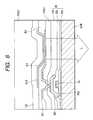
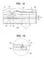
- FIG. 15is a sectional view for describing the structure near a pixel of a display module that uses an organic light emitting diode.
- This display moduleis constituted by piling up a polycrystalline silicon semiconductor layer PSI that uses low temperature polycrystalline silicon as an ideal material, a first insulation layer IS 1 , a gate line (gate electrode) GL that is a scanning line, a second insulation layer IS 2 , a source electrode SD formed using an aluminum wire, a third insulation layer IS 3 , a passivation film PSV, a first electrode layer AD, an organic light emitting layer OLE, and a second electrode layer CD on a glass substrate SUB.
- a polycrystalline silicon semiconductor layer PSIthat uses low temperature polycrystalline silicon as an ideal material
- a first insulation layer IS 1that uses low temperature polycrystalline silicon as an ideal material
- a gate line (gate electrode) GLthat is a scanning line
- a second insulation layer IS 2a source electrode SD formed using an aluminum wire
- a third insulation layer IS 3a pass
- this thin film transistoris a driver transistor
- this thin film transistoris a driver transistor
- an organic light emitting diode formed using the first electrode layer AD connected to the source electrode SD, the organic light emitting layer OLE, and the second electrode layer CDemits light and the light L is incident on the outside from the substrate SUB.
- the edge of the first electrode layer AD or the edge of the second electrode layer CDis close to the second electrode layer CD or the first electrode layer AD via the thin organic light emitting layer OLE. In such structure, the following problem is easy to occur.
- FIG. 16is an enlarged drawing of the part shown by the A of FIG. 15 .
- an electric fieldis concentrated on the edge of the first electrode layer AD or the second electrode layer CD.
- the organic light emitting layer OLEis dielectrically broken down between the second electrode layer CD and the first electrode layer AD and leakage current X is easy to occur.
- leakage current Xoccurs, a high current flows from the current supply line CSL into a thin film transistor and will damage the thin film transistor.
- the thin film transistoris damaged, what is called a point defect occurs and a display fault will be produced.
- a scanning line, a data line or two thin film transistors, and a capacitorare formed on a substrate SUB in a multi-layered structure, even if the top of the second electrode layer coated with the organic light emitting layer is flat, the flatness of the periphery is extremely low. Therefore, dispersion occurs in the space between the first electrode layer and the second electrode layer, and the same leakage current as above occurs in the part where both electrode layers are adjacent each other.
- An organic light emitting layeris coated using a method, such as printing coating, coating using ink jet, or spin coating. Because the coating material of the organic light emitting layer used in such coating has fluidity, if the flatness of a coating surface and its periphery is low, the coated organic emitting material flows into the periphery or is piled up in a part of the periphery. Accordingly, it is difficult to form the organic light emitting layer in uniform thickness and through a necessary and sufficient spread over the predetermined pixel region.
- an organic light emitting layerdiffers in its thickness and spread every pixel, a difference occurs in each emitting luminance and the brightness in all screen areas becomes uneven, thereby disabling acquisition of a high image quality display.
- An object of the present inventionis to provide a display module that enables a high quality display by preventing the leakage current generated between a first electrode layer and a second electrode layer that constitute a pixel via an organic light emitting layer and forming the organic light emitting layer that constitutes the pixel in uniform thickness and through a necessary and sufficient spread over the predetermined pixel region.
- the present inventionprevents the generation of leakage current between a first electrode layer and a second electrode layer, as described above, by providing an interlayer insulation layer between an edge of the first electrode layer and an organic light emitting layer that constitute a pixel and sufficiently securing the distance between the edge and the second electrode layer.
- the present inventionimproves flatness as a whole by using a resin material with fluidity in the interlayer insulation layer, forming an organic light emitting layer accommodation unit on this interlayer insulation layer, and forming the coated organic light emitting layer in uniform thickness and through a necessary and sufficient spread over the predetermined pixel region.
- a display moduleis provided with multiple scanning lines arranged in a matrix on a substrate, multiple data lines that intersect the multiple scanning lines, and a current supply line that supplies display current to a pixel and has a pixel every intersection unit of each of the scanning lines and each of the data lines, wherein
- the interlayer insulation layerprovides an aperture in which the organic light emitting layer is accommodated in the coating region of the organic light emitting layer that constitutes the light emission unit.
- the interlayer insulation layeris formed by being coated with a fluidity resin.
- the display modulehas at least either an insulation layer or a passivation film between at least a part of the first electrode layer and the substrate, and an aperture in which the organic light emitting layer is accommodated in at least either the insulation layer or the passivation film.
- the interlayer insulation layeris formed by covering an edge of the first electrode layer.
- the interlayer insulation layeris formed by covering all edges of the first electrode layer.
- the distance between the edge of the first electrode layer and the edge of the second electrode layeris secured sufficiently and the generation of leakage current between the first electrode layer and the second electrode layer is prevented via an organic light emitting layer.
- a display moduleis provided with multiple scanning lines arranged in a matrix on a substrate, multiple data lines that intersect the multiple scanning lines, and a current supply line that supplies display current to the pixel and has a pixel every intersection unit of each of the scanning lines and each of the data lines, wherein
- the interlayer insulation layeris formed by covering an edge of the first electrode layer.
- the interlayer insulation layeris formed by covering all edges of the first electrode layer.
- the first electrode layeris formed using ITO.
- the present inventionis not limited to the above configuration and the configuration of the embodiments described later, and, needless to say, enables various modifications without deviating from a technical idea of the present invention.
- FIG. 1is a typical sectional view near a pixel for describing the configuration of a first embodiment of a display module according to the present invention
- FIG. 2is a typical drawing for describing a cross section near a pixel in the order of a production process in which an example of the production process of the display module of the first embodiment is described in the display module according to the present invention
- FIG. 3is a typical drawing in the vicinity of a pixel for describing a light emission mechanism of the display module according to the present invention
- FIG. 4is a typical sectional view in the vicinity a pixel for describing the configuration of a second embodiment of the display module according to the present invention
- FIG. 5is a typical sectional view in the vicinity a pixel for describing the configuration of a third embodiment of the display module according to the present invention.
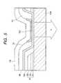
- FIG. 6is a typical sectional view in the vicinity a pixel for describing the configuration of a fourth embodiment of the display module according to the present invention.
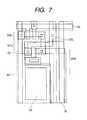
- FIG. 7is a top plan view near a pixel for describing an example of the circuit configuration of the display module according to the present invention.
- FIG. 8is a typical sectional view in the vicinity a pixel for describing the configuration of a fifth embodiment of the display module according to the present invention.
- FIG. 9is a top plan view near a pixel for describing an example of the circuit configuration of the display module according to the present invention shown in FIG. 8 ;
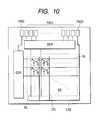
- FIG. 10is a top plan view for typically describing an example of the circuit placement of the display module according to the present invention.
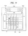
- FIG. 11is a top plan view for typically describing an example of the aperture position of a pixel provided corresponding to the circuit placement of FIG. 10 ;
- FIG. 12is a block diagram for typically describing a configuration example of a conventional display module using an organic emitting device
- FIG. 13is an explanatory drawing of the pixel configuration in FIG. 12 ;
- FIG. 14is the same block diagram as FIG. 13 for typically describing another configuration example of the conventional display module that uses the organic emitting device;
- FIG. 15is a sectional view for describing the structure in the vicinity of a pixel of a display module that uses the organic emitting device.
- FIG. 16is an enlarged drawing of the part showing by A of FIG. 15 .
- An organic light emitting layer provided in each pixel that is not shown, but is described laterperforms a monochromatic or color display by emitting light in the luminance that is proportional to a current value and a color (including white) that depends on the organic materials and performs the color display that emits by combining a color filter, such as red, green, or blue with an organic layer that emits white light.
- a color filtersuch as red, green, or blue
- FIG. 1is a typical sectional view near a pixel for describing the configuration of a first example of a display module according to the present invention.
- the display module that uses an active matrix type organic light emitting diode (OLED) shown in FIG. 1has a thin film transistor of each element formed on an insulating substrate SUB, such as glass, using a polycrystalline silicon layer PSI.
- the thin film transistor of this embodimenthas a first insulation layer IS 1 , a gate line (scanning line) GL, a second insulation layer IS 2 , a source line SD, and a third insulation layer IS 3 on the polycrystalline silicon layer PSI, and an ITO pattern that becomes a first electrode layer is formed on a passivation film PSV formed on the upper layer unit of the third insulation layer IS 3 .
- This first electrode layer ADis connected to the source line SD through a contact hole perforated by piercing into the passivation film PSV and the third layer IS 3 .
- an interlayer insulation layer ILI with fluidity composed of an acrylic resinis coated and the smoothness of the surface is improved.
- an apertureis formed in the pixel region of the interlayer insulation layer ILI by a processing means, such as a photolithographic technique. This aperture is formed only in the area required for providing an organic light emitting layer inside the pattern of the first electrode layer AD.
- a recessed part in which the interlayer insulation layer ILI becomes an inside wall having a taper and a flat first electrode layer AD is exposed at the bottomis formed in the pixel region.
- an organic light emitting layer OLEBy coating this recessed part with an organic light emitting layer OLE, a uniform organic light emitting layer OLE in necessary thickness is accommodated and formed in the pixel region. Further, the organic light emitting layer OLE coated around the pixel region is isolated from the first electrode layer AD in the interlayer insulation layer ILI.
- the upper layeris covered and a second electrode layer CD is formed.
- a metal filmis suitable for this second electrode layer CD. Because the interlayer insulation layer ILI has a taper, what is called step disconnection is difficult to occur in the organic light emitting layer OLE and the second electrode layer CD applied on it.
- the second electrode layer CD formed at an edge around the organic light emitting layer OLEis isolated from the first electrode layer AD including the edge. Accordingly, the generation of leakage current between the edge of either the first electrode layer AD or the second electrode layer CD or between the edge of both electrode layers is prevented sufficiently.
- the distance between an edge of a first electrode layer and a second electrode layer that constitute a pixelis secured sufficiently and the generation of leakage current between the first electrode and the second electrode layer via an organic light emitting layer is prevented. Further, because the organic light emitting layer that constitutes the pixel is formed in uniform thickness and through a necessary and sufficient spread over the predetermined pixel region a display module that enables a high quality display is obtained.
- FIG. 2is a typical drawing for describing a cross section near a pixel in the order of a production process in which an example of the production process of the display module of the first embodiment is described in the display module according to the present invention.
- This embodimentuses a thin film transistor of what is called the top gate structure, but also uses a thin film transistor of what is called the bottom gate structure in the same manner. This process is described below in the order of steps (1) to (11).
- a polycrystalline silicon semiconductor layer PSIis patterned on a glass substrate SUB and laser annealing for crystallization is applied.
- a first insulation layer IS 1is formed on it.
- a gate line (scanning line) GLis formed by depositing and patterning a conductive thin film, such as titanium (Ti) or tungsten (W).
- a second insulation layer IS 2is formed and a contact hole is perforated at a necessary place.
- An aluminum wire that becomes a source electrode SDis formed (as the need arises, the top and bottom of an aluminum thin film are sandwiched between materials of titanium (Ti) or tungsten (W).
- a third insulation layer IS 3is formed by covering an aluminum wire.
- a passivation film PSVis formed using p-Sin. A contact hole that pierces into this passivation film PSV and the third insulation layer IS 3 and reaches the source electrode SD is perforated.
- a first electrode ADis formed by depositing ITO. This first electrode layer AD is connected to the source electrode SD via the contact hole.
- An interlayer insulation layer ILI for insulating an organic light emitting layer from an edge of the first electrode layer ADis formed. Further, an aperture is perforated in the pixel region required for light emission and at a place necessary for external connection in the interlayer insulation layer ILI.
- the interlayer insulation layer ILIuses an acrylic resin with fluidity. A taper is formed on an inside wall by applying heat when the aperture pattern of the pixel region is formed.
- the aperture of the pixel regionis coated with an organic light emitting layer OLE.
- the coating of the organic light emitting layer OLEis performed by a method, such as mask printing or ink jet.
- a metal layeris formed by covering an organic light emitting layer OLE and a second electrode layer CD.
- a display moduleis completed by being sealed in a sealing can or with a proper member, such as glass and ceramics, and being put into a module.
- FIG. 3is a typical drawing in the vicinity of a pixel for describing a light emission mechanism of the display module according to the present invention.
- the same reference symbol as FIG. 1corresponds to the same part.
- the arrow mark using the reference symbol I of the drawingshows a path of the current that yields to light emission.
- a thin film transistor TFTis a driver transistor.
- this thin film transistor TFTis selected by a gate line GL, the current I having a current value of a gray scale that matches a data signal held in a capacitor is supplied to a first electrode layer AD of an organic light emitting diode OLED through the thin film transistor TFT (see FIG. 14 ).
- an electron from a second electrode layer CD and a hole from a first electrode layer ADare recombined in the organic light emitting layer OLE and light L of a spectrum that matches material characteristics of the organic light emitting layer OLE is emitted.
- the first electrode layer ADis independent every pixel and the second electrode layer is formed all over in a film shape concerning all pixels.
- a two-dimensional display moduleis constituted by arranging such many pixels in a matrix.
- FIG. 4is a typical sectional view near a pixel for describing the configuration of the second example of the display module according to the present invention.
- the same reference symbol as FIG. 1corresponds to the same function part.
- the film thickness of the interlayer insulation layer ILI shown in FIG. 1is about 1 ⁇ m, whereas the volume of an aperture (recessed part) in which an organic light emitting layer OLE is accommodated is increased by thickening the film thickness 2 or 3 ⁇ m, for example.
- This embodimenthas the structure suitable when an organic light emitting layer OLE is coated using an inkjet system.
- an organic emitting materialsplashes from an inkjet nozzle into the aperture of an interlayer insulation layer and reaches a first electrode layer AD with the material diluted in some solvent and with the volume increased.
- an organic light emitting layer applied to each pixelcan be isolated clearly and deterioration in the saturation of a luminous color can be prevented in addition to the effect of the embodiment described above.
- mask printing and spin coating systems as well as an inkjet systemcan be applied to the coating of the organic light emitting layer OLE.
- FIG. 5is a typical sectional view near a pixel for describing the configuration of a third example of the display module according to the present invention.
- the same reference symbol as FIG. 1corresponds to the same function part.
- This embodimentfurther increases the volume of an aperture (recessed part) in which the insulation layer IS and the passivation film PSV are removed from the pixel region and an organic light emitting layer OLE is accommodated.
- the interlayer insulation layer ILIis formed in the inside wall of the recessed part that is an aperture.
- the insulation layer of an organic light emitting layer OLEis formed on a first electrode AD and opens at the bottom of the recessed part.
- the organic light emitting layer OLEis accommodated in this aperture and the second electrode layer CD is formed on it.
- This embodimentis also suitable when an organic light emitting layer OEL is coated using an inkjet system and, in addition to the effect of the example, an organic light emitting layer applied to each pixel can be isolated clearly and deterioration in the saturation of a luminous color can be prevented.
- mask printing and spin coating systems as well as the inkjet systemcan be applied to the coating of the organic light emitting layer OLE.
- FIG. 6is a typical sectional view near a pixel for describing the configuration of a fourth embodiment of the display module according to the present invention.
- the same reference symbol as FIG. 1corresponds to the same function part.
- a second passivation film PSV 2is further formed on a passivation film PSV (equals to a first passivation film PSV 1 ) in the first embodiment described in FIG. 1 .
- Another configurationis the same configuration as FIG. 1 .
- the reliability of a display modulecan be improved further.
- the second passivation film PSV 2can also be formed toward the second or third embodiments in the same manner.
- FIG. 7is a top plain view near a pixel for describing an example of the circuit configuration of the display module according to the present invention.
- a pixelis formed in the area enclosed by a scanning line (gate line) GL and a data line DL.
- the reference symbol ADis a first electrode layer (anode here) and CSL is a current supply line.
- a pixel circuithas a first thin film transistor TFT 1 (switching transistor), a second thin film transistor TFT 2 (driver transistor), and a capacitor CPR. Further, an aperture DE that accommodates an organic light emitting layer is provided in the part where the pixel circuit and each wiring are prevented.
- FIG. 8is a typical sectional view for describing the configuration of a fifth embodiment of the circuit configuration of the display module according to the present invention.
- the same reference symbol as FIG. 1corresponds to the same function part.
- This embodimenthas the configuration in which the exit direction of light emission is set at the opposite side with a substrate.
- CD′indicates a first electrode layer (cathode here) formed using a metal thin film
- AD′indicates a second electrode (anode here) formed using a transparent conductive film, such as ITO.
- the emission light in an organic light emitting layer OLEexits from the second electrode layer AD′.
- a sealing member that is not shown, but is provided on the side of the second electrode layer AD′uses a transparent member, such as glass.
- FIG. 9is a top plan drawing near a pixel for describing an example of the circuit configuration of the display module according to the present invention shown in FIG. 8 .
- the same reference symbol as FIG. 7corresponds to the same function part.
- a pixelis formed in the area enclosed by a scanning line (gate line) GL and a data line DL in the same manner as the above embodiment.
- an aperture DE that accommodates an organic light emitting layer OLEneeds not to be provided in the part where the pixel circuit and each wiring are prevented. Accordingly, because the configuration of this embodiment is obtained, there is an advantage that a pixel having a high aperture ratio and a wide area can be formed. On the whole, a display module having a bright screen, and a display module having low consumption power and a long life span can be obtained.
- FIG. 10is a top plan drawing for typically describing an example of the circuit placement of the display module according to the present invention
- FIG. 11is a top plan view for typically describing an example of the aperture position of a pixel provided corresponding to the circuit placement of FIG. 10 .
- Each pixelis formed in the part enclosed by a scanning line GL driven in a scanning driving circuit GDR and a data line DL driven in a data driving circuit DDR and arranged in a matrix shape.
- a current supply line CSLbranches at the outside of a display region AR from a current supply bus line CSB and arranged in parallel to the data line DL for each pixel.
- PADis a pad for externally supplying a signal and power to a display module via a flexible printed board.
- PAD 1indicates a pad for a data driver
- PAD 2indicates a pad for a scanning driver
- PAD 3indicates a current supply pad. Even each part of these pads forms an aperture in an insulation layer and a passivation film.
- the aperture for applying an organic light emitting layer that constitutes the light emission area of a pixelis arranged in a matrix shape corresponding to each pixel as shown in FIG. 11 . Further, the reliability of a display module is improved by also providing an aperture unit in a sealing unit that turns around a display region AR as the need arises and improving the adhesion between a substrate and the sealing unit. Besides, an aperture that is a contact hole for connecting a second electrode layer to the bottom wiring layer is also formed.
- the present inventionis not limited to a display module that uses the OLED described above, and can also be applied to another display module that performs a display in the same light emission operation as the OLED.
- the present inventionbecause the leakage current generated between a first electrode layer and a second electrode layer that constitute a pixel via an organic light emitting layer is prevented and the organic light emitting layer that constitutes the pixel is formed in uniform thickness and through a necessary and sufficient spread over the predetermined pixel region, a display module that enables a high quality display can be provided.
Landscapes
- Engineering & Computer Science (AREA)
- Microelectronics & Electronic Packaging (AREA)
- Physics & Mathematics (AREA)
- General Physics & Mathematics (AREA)
- Theoretical Computer Science (AREA)
- Optics & Photonics (AREA)
- Computer Hardware Design (AREA)
- Geometry (AREA)
- Electroluminescent Light Sources (AREA)
- Devices For Indicating Variable Information By Combining Individual Elements (AREA)
Abstract
Description
- the pixel has an active element selected by the scanning line, a data holding element that holds a data signal supplied from the data line by the turn-on of this active element, and an emitting device that emits light by the current supplied from the current supply line in accordance with the data signal held by the data holding element,
- the emitting device has a first electrode layer driven by the active element, an organic light emitting layer applied on the first electrode layer, and a second electrode layer formed on the organic light emitting layer, and
- an interlayer insulation layer is provided between the first electrode layer and the second electrode layer in the periphery of a light emission unit formed in the lamination structure of the first electrode layer, the organic light emitting layer, and the second electrode layer.
- the pixel has an active element selected by the scanning line, a data holding element that holds a data signal supplied from the data line by the turn-on of this active element, and an emitting device that emits light by the current supplied from the current supply line in accordance with the data signal held by the data holding element,
- the emitting device has a first electrode layer driven by the active element, an organic light emitting layer applied on the first electrode layer, and a second electrode layer formed on the organic light emitting layer, and
- an interlayer insulation layer formed by coating a fluidity resin is provided between the first electrode layer and the second electrode layer in the periphery of a light emission unit formed in the lamination structure of the first electrode layer, the organic light emitting layer, and the second electrode layer.
Claims (7)
Priority Applications (9)
| Application Number | Priority Date | Filing Date | Title |
|---|---|---|---|
| US11/113,173US6977463B2 (en) | 2001-03-28 | 2005-04-25 | Display module |
| US11/245,203US20060132029A1 (en) | 2001-03-28 | 2005-10-07 | Display module |
| US12/056,638US8232934B2 (en) | 2001-03-28 | 2008-03-27 | Display module |
| US13/524,815US8766884B2 (en) | 2001-03-28 | 2012-06-15 | Display module |
| US14/292,421US9214504B2 (en) | 2001-03-28 | 2014-05-30 | Display module |
| US14/620,117US9735220B2 (en) | 2001-03-28 | 2015-02-11 | Display module |
| US14/798,416US9627464B2 (en) | 2001-03-28 | 2015-07-13 | Display module |
| US14/944,524US9653529B2 (en) | 2001-03-28 | 2015-11-18 | Display module |
| US15/644,942US10062744B2 (en) | 2001-03-28 | 2017-07-10 | Display module |
Applications Claiming Priority (2)
| Application Number | Priority Date | Filing Date | Title |
|---|---|---|---|
| JP2001092818AJP3608613B2 (en) | 2001-03-28 | 2001-03-28 | Display device |
| JP2001-092818 | 2001-03-28 |
Related Child Applications (1)
| Application Number | Title | Priority Date | Filing Date |
|---|---|---|---|
| US11/113,173ContinuationUS6977463B2 (en) | 2001-03-28 | 2005-04-25 | Display module |
Publications (2)
| Publication Number | Publication Date |
|---|---|
| US20020140643A1 US20020140643A1 (en) | 2002-10-03 |
| US6888304B2true US6888304B2 (en) | 2005-05-03 |
Family
ID=18947222
Family Applications (10)
| Application Number | Title | Priority Date | Filing Date |
|---|---|---|---|
| US10/102,910Expired - LifetimeUS6888304B2 (en) | 2001-03-28 | 2002-03-22 | Display module |
| US11/113,173Expired - LifetimeUS6977463B2 (en) | 2001-03-28 | 2005-04-25 | Display module |
| US11/245,203AbandonedUS20060132029A1 (en) | 2001-03-28 | 2005-10-07 | Display module |
| US12/056,638Expired - LifetimeUS8232934B2 (en) | 2001-03-28 | 2008-03-27 | Display module |
| US13/524,815Expired - LifetimeUS8766884B2 (en) | 2001-03-28 | 2012-06-15 | Display module |
| US14/292,421Expired - Fee RelatedUS9214504B2 (en) | 2001-03-28 | 2014-05-30 | Display module |
| US14/620,117Expired - Fee RelatedUS9735220B2 (en) | 2001-03-28 | 2015-02-11 | Display module |
| US14/798,416Expired - Fee RelatedUS9627464B2 (en) | 2001-03-28 | 2015-07-13 | Display module |
| US14/944,524Expired - Fee RelatedUS9653529B2 (en) | 2001-03-28 | 2015-11-18 | Display module |
| US15/644,942Expired - LifetimeUS10062744B2 (en) | 2001-03-28 | 2017-07-10 | Display module |
Family Applications After (9)
| Application Number | Title | Priority Date | Filing Date |
|---|---|---|---|
| US11/113,173Expired - LifetimeUS6977463B2 (en) | 2001-03-28 | 2005-04-25 | Display module |
| US11/245,203AbandonedUS20060132029A1 (en) | 2001-03-28 | 2005-10-07 | Display module |
| US12/056,638Expired - LifetimeUS8232934B2 (en) | 2001-03-28 | 2008-03-27 | Display module |
| US13/524,815Expired - LifetimeUS8766884B2 (en) | 2001-03-28 | 2012-06-15 | Display module |
| US14/292,421Expired - Fee RelatedUS9214504B2 (en) | 2001-03-28 | 2014-05-30 | Display module |
| US14/620,117Expired - Fee RelatedUS9735220B2 (en) | 2001-03-28 | 2015-02-11 | Display module |
| US14/798,416Expired - Fee RelatedUS9627464B2 (en) | 2001-03-28 | 2015-07-13 | Display module |
| US14/944,524Expired - Fee RelatedUS9653529B2 (en) | 2001-03-28 | 2015-11-18 | Display module |
| US15/644,942Expired - LifetimeUS10062744B2 (en) | 2001-03-28 | 2017-07-10 | Display module |
Country Status (4)
| Country | Link |
|---|---|
| US (10) | US6888304B2 (en) |
| JP (1) | JP3608613B2 (en) |
| KR (1) | KR100502747B1 (en) |
| TW (1) | TW569165B (en) |
Cited By (19)
| Publication number | Priority date | Publication date | Assignee | Title |
|---|---|---|---|---|
| US20030197664A1 (en)* | 1999-10-26 | 2003-10-23 | Semiconductor Energy Laboratory Co., Ltd. | Electro-optical device |
| US20040119419A1 (en)* | 2002-12-11 | 2004-06-24 | Kazuhiko Kai | Organic EL display device |
| US20050045882A1 (en)* | 2003-08-28 | 2005-03-03 | Park Sang-Il | Organic electroluminescent display |
| US20050052393A1 (en)* | 2003-08-26 | 2005-03-10 | Seiko Epson Corporation | Method of driving liquid crystal display device, liquid crystal display device, and portable electronic apparatus |
| US20050067947A1 (en)* | 2001-05-10 | 2005-03-31 | Kazuhiko Hayashi | Light-emitting body, light emitting device and light-emitting display |
| US20050145861A1 (en)* | 2003-12-26 | 2005-07-07 | Semiconductor Energy Laboratory Co., Ltd. | Light emitting device |
| US20050161680A1 (en)* | 2004-01-26 | 2005-07-28 | Semiconductor Energy Laboratory Co., Ltd. | Light-emitting device |
| US20050285100A1 (en)* | 2004-06-28 | 2005-12-29 | Chang-Yong Jeong | Organic light emitting display and method of fabricating the same |
| US20060186402A1 (en)* | 2004-09-20 | 2006-08-24 | Winters Dustin L | Providing driving current arrangement for OLED device |
| US20090001380A1 (en)* | 2007-06-27 | 2009-01-01 | Samsung Sdi Co., Ltd. | Thin film transistor, method of fabricating the same, organic light emitting diode display device including the same and method of fabricating the same |
| US20090021497A1 (en)* | 2004-10-14 | 2009-01-22 | Daktronics, Inc. | Flexible pixel element and signal distribution means |
| US20090021529A1 (en)* | 2004-10-14 | 2009-01-22 | Daktronics, Inc. | Flexible pixel element fabrication and sealing method |
| US8001455B2 (en) | 2004-10-14 | 2011-08-16 | Daktronics, Inc. | Translation table |
| US8106923B2 (en) | 2004-10-14 | 2012-01-31 | Daktronics, Inc. | Flexible pixel hardware and method |
| US20140264306A1 (en)* | 2001-03-28 | 2014-09-18 | Japan Display Inc. | Display module |
| US8847483B2 (en) | 2005-10-17 | 2014-09-30 | Semiconductor Energy Laboratory Co., Ltd. | Semiconductor device and manufacturing method thereof |
| US8890204B2 (en) | 2005-03-22 | 2014-11-18 | Semiconductor Energy Laboratory Co., Ltd. | Light emitting device |
| US20170146868A1 (en)* | 2015-11-20 | 2017-05-25 | Samsung Display Co., Ltd. | Liquid-crystal display device |
| US9773818B2 (en) | 2005-10-14 | 2017-09-26 | Semiconductor Energy Laboratory Co., Ltd. | Display device having transparent conductive film and metal film |
Families Citing this family (55)
| Publication number | Priority date | Publication date | Assignee | Title |
|---|---|---|---|---|
| TW478169B (en)* | 1999-07-16 | 2002-03-01 | Seiko Epson Corp | Electro optical device and the projection display device using the same |
| US7211828B2 (en) | 2001-06-20 | 2007-05-01 | Semiconductor Energy Laboratory Co., Ltd. | Light emitting device and electronic apparatus |
| TW548860B (en) | 2001-06-20 | 2003-08-21 | Semiconductor Energy Lab | Light emitting device and method of manufacturing the same |
| US7579771B2 (en) | 2002-04-23 | 2009-08-25 | Semiconductor Energy Laboratory Co., Ltd. | Light emitting device and method of manufacturing the same |
| US7786496B2 (en) | 2002-04-24 | 2010-08-31 | Semiconductor Energy Laboratory Co., Ltd. | Semiconductor device and method of manufacturing same |
| JP2003317971A (en) | 2002-04-26 | 2003-11-07 | Semiconductor Energy Lab Co Ltd | Light emitting device and manufacturing method thereof |
| US7897979B2 (en) | 2002-06-07 | 2011-03-01 | Semiconductor Energy Laboratory Co., Ltd. | Light emitting device and manufacturing method thereof |
| JP4216008B2 (en) | 2002-06-27 | 2009-01-28 | 株式会社半導体エネルギー研究所 | LIGHT EMITTING DEVICE AND ITS MANUFACTURING METHOD, AND VIDEO CAMERA, DIGITAL CAMERA, GOGGLE TYPE DISPLAY, CAR NAVIGATION, PERSONAL COMPUTER, DVD PLAYER, ELECTRONIC GAME EQUIPMENT, OR PORTABLE INFORMATION TERMINAL HAVING THE LIGHT EMITTING DEVICE |
| US20040041757A1 (en)* | 2002-09-04 | 2004-03-04 | Ming-Hsiang Yang | Light emitting diode display module with high heat-dispersion and the substrate thereof |
| KR100544436B1 (en)* | 2002-11-26 | 2006-01-23 | 엘지.필립스 엘시디 주식회사 | Organic EL device and method of manufacturing the same |
| TWI283143B (en)* | 2002-12-03 | 2007-06-21 | Au Optronics Corp | Structure and method for reducing the resistance of power line, suitable for use in a LED displayer |
| TWI352553B (en)* | 2002-12-26 | 2011-11-11 | Semiconductor Energy Lab | Light emitting device and a method for manufacturi |
| JP4373086B2 (en)* | 2002-12-27 | 2009-11-25 | 株式会社半導体エネルギー研究所 | Light emitting device |
| JP4251874B2 (en)* | 2003-01-21 | 2009-04-08 | 三洋電機株式会社 | Electroluminescence display device |
| CN102709478B (en)* | 2003-03-26 | 2016-08-17 | 株式会社半导体能源研究所 | Light-emitting device |
| TW594653B (en)* | 2003-06-02 | 2004-06-21 | Toppoly Optoelectronics Corp | Low leakage thin film transistor circuit |
| US8937580B2 (en)* | 2003-08-08 | 2015-01-20 | Semiconductor Energy Laboratory Co., Ltd. | Driving method of light emitting device and light emitting device |
| KR100552975B1 (en)* | 2003-11-22 | 2006-02-15 | 삼성에스디아이 주식회사 | Active matrix organic light emitting display device and manufacturing method thereof |
| JP4287337B2 (en)* | 2003-11-24 | 2009-07-01 | 三星モバイルディスプレイ株式會社 | Organic electroluminescent display device and manufacturing method thereof |
| KR100741962B1 (en)* | 2003-11-26 | 2007-07-23 | 삼성에스디아이 주식회사 | Flat Panel Display |
| KR100611152B1 (en)* | 2003-11-27 | 2006-08-09 | 삼성에스디아이 주식회사 | Flat Panel Display |
| US7274044B2 (en) | 2004-01-26 | 2007-09-25 | Semiconductor Energy Laboratory Co., Ltd. | Light emitting device |
| WO2005093695A1 (en)* | 2004-03-26 | 2005-10-06 | Pioneer Corporation | Subpixel |
| US7692378B2 (en)* | 2004-04-28 | 2010-04-06 | Semiconductor Energy Laboratory Co., Ltd. | Display device including an insulating layer with an opening |
| KR100635066B1 (en)* | 2004-06-03 | 2006-10-16 | 삼성에스디아이 주식회사 | Organic electroluminescent display and manufacturing method thereof |
| KR100699998B1 (en) | 2004-09-23 | 2007-03-26 | 삼성에스디아이 주식회사 | Organic electroluminescent device and manufacturing method thereof |
| JP4645311B2 (en)* | 2005-06-03 | 2011-03-09 | 凸版印刷株式会社 | Organic EL element manufacturing method and organic EL element manufacturing apparatus |
| TWI280073B (en)* | 2005-09-15 | 2007-04-21 | Au Optronics Corp | Organic light emitting diode display panel |
| US7990047B2 (en)* | 2005-10-28 | 2011-08-02 | Samsung Electronics Co., Ltd. | Organic light emitting diode display and method of manufacturing the same |
| WO2007077715A1 (en) | 2006-01-05 | 2007-07-12 | Konica Minolta Holdings, Inc. | Bottom emission type organic electro luminescence panel |
| US8138075B1 (en) | 2006-02-06 | 2012-03-20 | Eberlein Dietmar C | Systems and methods for the manufacture of flat panel devices |
| US8035309B2 (en)* | 2006-03-23 | 2011-10-11 | Koninklijke Philips Electronics N.V. | Light emitting device |
| KR101367140B1 (en)* | 2006-12-26 | 2014-03-14 | 삼성디스플레이 주식회사 | Display device and manufacturing method of the same |
| KR100932937B1 (en) | 2008-04-01 | 2009-12-21 | 삼성모바일디스플레이주식회사 | OLED display and manufacturing method thereof |
| JP2010153813A (en)* | 2008-11-18 | 2010-07-08 | Semiconductor Energy Lab Co Ltd | Light-emitting device, method of manufacturing the same, and portable telephone |
| JP5917127B2 (en)* | 2011-12-19 | 2016-05-11 | 株式会社ジャパンディスプレイ | Liquid crystal display |
| CN104126332B (en)* | 2012-02-21 | 2016-12-07 | 株式会社日本有机雷特显示器 | Organic luminescent device and manufacture method thereof |
| US20130321433A1 (en)* | 2012-05-31 | 2013-12-05 | Qualcomm Mems Technologies, Inc. | Frontlight device with integrated electrical wiring |
| JP2014029814A (en)* | 2012-07-31 | 2014-02-13 | Sony Corp | Display device and electronic equipment |
| KR102131963B1 (en)* | 2013-10-15 | 2020-07-09 | 삼성디스플레이 주식회사 | Organic light-emitting display apparatus |
| JP2015169760A (en)* | 2014-03-06 | 2015-09-28 | 株式会社ジャパンディスプレイ | Manufacturing method of display device, display device, and display device formation substrate |
| KR20150137214A (en)* | 2014-05-28 | 2015-12-09 | 삼성디스플레이 주식회사 | Organic light-emitting display apparatus and manufacturing the same |
| CN104183606A (en) | 2014-08-07 | 2014-12-03 | 京东方科技集团股份有限公司 | Display substrate, manufacturing method of display substrate, and display device |
| JP6673731B2 (en) | 2016-03-23 | 2020-03-25 | 株式会社ジャパンディスプレイ | Display device and manufacturing method thereof |
| CN105977279B (en)* | 2016-07-07 | 2020-12-01 | 京东方科技集团股份有限公司 | Organic electroluminescent diode substrate and preparation method thereof, and display device |
| KR102711850B1 (en)* | 2016-11-30 | 2024-10-02 | 엘지디스플레이 주식회사 | Anisotropic conductive film and display device comprising the same |
| KR101992917B1 (en)* | 2016-11-30 | 2019-06-25 | 엘지디스플레이 주식회사 | Substrate for display, organic light emitting display device including the same, and method of manufacturing the same |
| KR102772195B1 (en)* | 2017-02-28 | 2025-02-26 | 삼성디스플레이 주식회사 | Display apparatus and method for manufacturing the same |
| CN108766975B (en)* | 2018-04-28 | 2021-02-02 | 上海天马有机发光显示技术有限公司 | Display panel and electronic equipment |
| CN108878677B (en)* | 2018-06-13 | 2020-04-03 | 上海天马有机发光显示技术有限公司 | Display panel and display device |
| TWI684053B (en)* | 2018-06-21 | 2020-02-01 | 友達光電股份有限公司 | Display device and method of fabricating the same |
| KR102661283B1 (en)* | 2018-11-26 | 2024-05-02 | 삼성디스플레이 주식회사 | Display substrate, method of manufacturing the same, and display device including the same |
| KR102741002B1 (en) | 2020-04-29 | 2024-12-12 | 삼성디스플레이 주식회사 | Organic light-emitting display and method for manufacturing the same |
| CN117940845A (en)* | 2021-09-16 | 2024-04-26 | 金泰克斯公司 | Electro-optical element electrodes |
| KR20240048048A (en) | 2022-10-04 | 2024-04-15 | 삼성디스플레이 주식회사 | Display device |
Citations (2)
| Publication number | Priority date | Publication date | Assignee | Title |
|---|---|---|---|---|
| JPH10301100A (en) | 1997-02-27 | 1998-11-13 | Seiko Epson Corp | Liquid crystal device, manufacturing method thereof, and projection display device |
| JP2001005426A (en) | 1999-06-23 | 2001-01-12 | Semiconductor Energy Lab Co Ltd | EL display device and electronic device |
Family Cites Families (25)
| Publication number | Priority date | Publication date | Assignee | Title |
|---|---|---|---|---|
| JP3242941B2 (en) | 1991-04-30 | 2001-12-25 | 富士ゼロックス株式会社 | Active EL matrix and driving method thereof |
| JPH0634998A (en)* | 1992-07-15 | 1994-02-10 | Toshiba Corp | Liquid crystal display |
| US5586695A (en) | 1993-10-07 | 1996-12-24 | Labus; Rainer H. | Sprayed liquid dispensing apparatus |
| US5684365A (en) | 1994-12-14 | 1997-11-04 | Eastman Kodak Company | TFT-el display panel using organic electroluminescent media |
| US5550066A (en) | 1994-12-14 | 1996-08-27 | Eastman Kodak Company | Method of fabricating a TFT-EL pixel |
| DE69535970D1 (en) | 1994-12-14 | 2009-08-06 | Eastman Kodak Co | Electroluminescent device with an organic electroluminescent layer |
| US5585695A (en)* | 1995-06-02 | 1996-12-17 | Adrian Kitai | Thin film electroluminescent display module |
| JP3281848B2 (en)* | 1996-11-29 | 2002-05-13 | 三洋電機株式会社 | Display device |
| CN100341042C (en) | 1997-02-17 | 2007-10-03 | 精工爱普生株式会社 | Display device |
| JP2000114540A (en)* | 1998-10-09 | 2000-04-21 | Sony Corp | Method for manufacturing electro-optical device and method for manufacturing electro-optical device |
| JP2000172198A (en) | 1998-12-01 | 2000-06-23 | Sanyo Electric Co Ltd | Electroluminescence display device |
| TW439387B (en) | 1998-12-01 | 2001-06-07 | Sanyo Electric Co | Display device |
| JP2000235355A (en) | 1999-02-15 | 2000-08-29 | Sony Corp | Optoelectronic device, drive substrate for optoelectronic device and their production |
| KR100316271B1 (en)* | 1999-05-27 | 2001-12-12 | 구본준, 론 위라하디락사 | An eld and fabricating method thereof |
| US6583471B1 (en) | 1999-06-02 | 2003-06-24 | Semiconductor Energy Laboratory Co., Ltd. | Semiconductor device having first and second insulating films |
| JP4651777B2 (en) | 1999-06-02 | 2011-03-16 | 株式会社半導体エネルギー研究所 | Method for manufacturing semiconductor device |
| JP3880244B2 (en) | 1999-06-04 | 2007-02-14 | キヤノン株式会社 | Light emitting device |
| JP2000348660A (en) | 1999-06-04 | 2000-12-15 | Shimadzu Corp | Electronic probe micro analyzer |
| JP5210473B2 (en)* | 1999-06-21 | 2013-06-12 | 株式会社半導体エネルギー研究所 | Display device |
| JP3386017B2 (en)* | 1999-10-15 | 2003-03-10 | 日本電気株式会社 | Method of manufacturing thin film transistor for liquid crystal display device |
| US6580094B1 (en)* | 1999-10-29 | 2003-06-17 | Semiconductor Energy Laboratory Co., Ltd. | Electro luminescence display device |
| JP2001147659A (en)* | 1999-11-18 | 2001-05-29 | Sony Corp | Display device |
| JP4421722B2 (en)* | 1999-12-14 | 2010-02-24 | シャープ株式会社 | Liquid crystal display device, driving method and driving circuit |
| JP2002098993A (en)* | 2000-09-25 | 2002-04-05 | Casio Comput Co Ltd | Liquid crystal display |
| JP3608613B2 (en)* | 2001-03-28 | 2005-01-12 | 株式会社日立製作所 | Display device |
- 2001
- 2001-03-28JPJP2001092818Apatent/JP3608613B2/ennot_activeExpired - Lifetime
- 2002
- 2002-03-14TWTW91104765Apatent/TW569165B/ennot_activeIP Right Cessation
- 2002-03-22USUS10/102,910patent/US6888304B2/ennot_activeExpired - Lifetime
- 2002-03-27KRKR10-2002-0016703Apatent/KR100502747B1/ennot_activeExpired - Lifetime
- 2005
- 2005-04-25USUS11/113,173patent/US6977463B2/ennot_activeExpired - Lifetime
- 2005-10-07USUS11/245,203patent/US20060132029A1/ennot_activeAbandoned
- 2008
- 2008-03-27USUS12/056,638patent/US8232934B2/ennot_activeExpired - Lifetime
- 2012
- 2012-06-15USUS13/524,815patent/US8766884B2/ennot_activeExpired - Lifetime
- 2014
- 2014-05-30USUS14/292,421patent/US9214504B2/ennot_activeExpired - Fee Related
- 2015
- 2015-02-11USUS14/620,117patent/US9735220B2/ennot_activeExpired - Fee Related
- 2015-07-13USUS14/798,416patent/US9627464B2/ennot_activeExpired - Fee Related
- 2015-11-18USUS14/944,524patent/US9653529B2/ennot_activeExpired - Fee Related
- 2017
- 2017-07-10USUS15/644,942patent/US10062744B2/ennot_activeExpired - Lifetime
Patent Citations (4)
| Publication number | Priority date | Publication date | Assignee | Title |
|---|---|---|---|---|
| JPH10301100A (en) | 1997-02-27 | 1998-11-13 | Seiko Epson Corp | Liquid crystal device, manufacturing method thereof, and projection display device |
| US6330044B1 (en) | 1997-02-27 | 2001-12-11 | Seiko Epson Corporation | Apparatus for providing light shielding in a liquid crystal display |
| JP2001005426A (en) | 1999-06-23 | 2001-01-12 | Semiconductor Energy Lab Co Ltd | EL display device and electronic device |
| US20020153844A1 (en) | 1999-06-23 | 2002-10-24 | Semiconductor Energy Laboratory Co., Ltd. | EL display device and electronic device |
Cited By (70)
| Publication number | Priority date | Publication date | Assignee | Title |
|---|---|---|---|---|
| US9391132B2 (en) | 1999-10-26 | 2016-07-12 | Semiconductor Energy Laboratory Co., Ltd. | Light emitting device |
| US7986094B2 (en) | 1999-10-26 | 2011-07-26 | Semiconductor Energy Laboratory Co., Ltd. | Electro-optical device with active matrix EL display |
| US20030197664A1 (en)* | 1999-10-26 | 2003-10-23 | Semiconductor Energy Laboratory Co., Ltd. | Electro-optical device |
| US8390190B2 (en) | 1999-10-26 | 2013-03-05 | Semiconductor Energy Laboratory Co., Ltd. | Electro-optical device with active matrix EL display |
| US7239083B2 (en)* | 1999-10-26 | 2007-07-03 | Semiconductor Energy Laboratory Co., Ltd. | Electro-optical device with active matrix type EL display |
| US8933624B2 (en) | 1999-10-26 | 2015-01-13 | Semiconductor Energy Laboratory Co., Ltd. | Light emitting device |
| US9214504B2 (en)* | 2001-03-28 | 2015-12-15 | Japan Display Inc. | Display module |
| US20140264306A1 (en)* | 2001-03-28 | 2014-09-18 | Japan Display Inc. | Display module |
| US10062744B2 (en) | 2001-03-28 | 2018-08-28 | Samsung Display Co., Ltd. | Display module |
| US9735220B2 (en) | 2001-03-28 | 2017-08-15 | Japan Display Inc. | Display module |
| US9627464B2 (en) | 2001-03-28 | 2017-04-18 | Japan Display Inc. | Display module |
| US9653529B2 (en) | 2001-03-28 | 2017-05-16 | Japan Display Inc. | Display module |
| US20050067947A1 (en)* | 2001-05-10 | 2005-03-31 | Kazuhiko Hayashi | Light-emitting body, light emitting device and light-emitting display |
| US7423382B2 (en)* | 2001-05-10 | 2008-09-09 | Samsung Sdi Co., Ltd. | Light-emitting body, light emitting device and light-emitting display |
| US7642701B2 (en) | 2002-12-11 | 2010-01-05 | Hitachi Displays, Ltd. | Organic EL display device |
| US20060158107A1 (en)* | 2002-12-11 | 2006-07-20 | Kazuhiko Kai | Organic EL display device |
| US7332854B2 (en) | 2002-12-11 | 2008-02-19 | Hitachi Displays, Ltd. | Organic EL display device |
| US7034453B2 (en)* | 2002-12-11 | 2006-04-25 | Hitachi Displays, Ltd. | Organic EL display device with arrangement to suppress degradation of the light emitting region |
| US8129902B2 (en) | 2002-12-11 | 2012-03-06 | Hitachi Displays, Ltd. | Organic EL display device comprising moisture diffusion reduction banks structure |
| US20040119419A1 (en)* | 2002-12-11 | 2004-06-24 | Kazuhiko Kai | Organic EL display device |
| US20100164372A1 (en)* | 2002-12-11 | 2010-07-01 | Kazuhiko Kai | Organic el display device |
| US8248338B2 (en) | 2003-08-26 | 2012-08-21 | Seiko Epson Corporation | Method of driving liquid crystal display device, liquid crystal display device, and portable electronic apparatus |
| US20050052393A1 (en)* | 2003-08-26 | 2005-03-10 | Seiko Epson Corporation | Method of driving liquid crystal display device, liquid crystal display device, and portable electronic apparatus |
| US7414602B2 (en)* | 2003-08-26 | 2008-08-19 | Seiko Epson Corporation | Method of driving liquid crystal display device, liquid crystal display device, and portable electronic apparatus |
| US7211826B2 (en)* | 2003-08-28 | 2007-05-01 | Samsung Sdi Co., Ltd. | Organic electroluminescent display |
| US20050045882A1 (en)* | 2003-08-28 | 2005-03-03 | Park Sang-Il | Organic electroluminescent display |
| US9583545B2 (en) | 2003-12-26 | 2017-02-28 | Semiconductor Energy Laboratory Co., Ltd. | Light emitting device |
| US20050145861A1 (en)* | 2003-12-26 | 2005-07-07 | Semiconductor Energy Laboratory Co., Ltd. | Light emitting device |
| US8624257B2 (en) | 2003-12-26 | 2014-01-07 | Semiconductor Energy Laboratory Co., Ltd. | Light emitting device |
| US9196638B2 (en) | 2003-12-26 | 2015-11-24 | Semiconductor Energy Laboratory Co., Ltd. | Light emitting device |
| US9911800B2 (en) | 2003-12-26 | 2018-03-06 | Semiconductor Energy Laboratory Co., Ltd. | Light emitting device |
| US7495257B2 (en) | 2003-12-26 | 2009-02-24 | Semiconductor Energy Laboratory Co., Ltd. | Light emitting device |
| US7977685B2 (en) | 2004-01-26 | 2011-07-12 | Semiconductor Energy Laboratory Co., Ltd. | Light-emitting device |
| US20050161680A1 (en)* | 2004-01-26 | 2005-07-28 | Semiconductor Energy Laboratory Co., Ltd. | Light-emitting device |
| US20080079362A1 (en)* | 2004-01-26 | 2008-04-03 | Semiconductor Energy Laboratory Co., Ltd. | Light-emitting device |
| US7315047B2 (en) | 2004-01-26 | 2008-01-01 | Semiconductor Energy Laboratory Co., Ltd. | Light-emitting device |
| US8669567B2 (en) | 2004-01-26 | 2014-03-11 | Semiconductor Energy Laboratory Co., Ltd. | Light-emitting device |
| US20050285100A1 (en)* | 2004-06-28 | 2005-12-29 | Chang-Yong Jeong | Organic light emitting display and method of fabricating the same |
| US7626204B2 (en)* | 2004-06-28 | 2009-12-01 | Samsung Mobile Display Co., Ltd. | Organic light emitting display and method of fabricating the same |
| US7195949B2 (en)* | 2004-09-20 | 2007-03-27 | Eastman Kodak Company | Providing driving current arrangement for OLED device |
| US20060186402A1 (en)* | 2004-09-20 | 2006-08-24 | Winters Dustin L | Providing driving current arrangement for OLED device |
| US8363038B2 (en) | 2004-10-14 | 2013-01-29 | Daktronics, Inc. | Flexible pixel hardware and method |
| US8552929B2 (en) | 2004-10-14 | 2013-10-08 | Daktronics, Inc. | Flexible pixel hardware and method |
| US8604509B2 (en) | 2004-10-14 | 2013-12-10 | Daktronics, Inc. | Flexible pixel element and signal distribution means |
| US20090021529A1 (en)* | 2004-10-14 | 2009-01-22 | Daktronics, Inc. | Flexible pixel element fabrication and sealing method |
| US8344410B2 (en) | 2004-10-14 | 2013-01-01 | Daktronics, Inc. | Flexible pixel element and signal distribution means |
| US9052092B2 (en) | 2004-10-14 | 2015-06-09 | Daktronics, Inc. | Sealed pixel assemblies, kits and methods |
| US8106923B2 (en) | 2004-10-14 | 2012-01-31 | Daktronics, Inc. | Flexible pixel hardware and method |
| US8552928B2 (en) | 2004-10-14 | 2013-10-08 | Daktronics, Inc. | Sealed pixel assemblies, kits and methods |
| US20090021497A1 (en)* | 2004-10-14 | 2009-01-22 | Daktronics, Inc. | Flexible pixel element and signal distribution means |
| US7868903B2 (en)* | 2004-10-14 | 2011-01-11 | Daktronics, Inc. | Flexible pixel element fabrication and sealing method |
| US20110102307A1 (en)* | 2004-10-14 | 2011-05-05 | Daktronics, Inc. | Sealed pixel assemblies, kits and methods |
| US8001455B2 (en) | 2004-10-14 | 2011-08-16 | Daktronics, Inc. | Translation table |
| US8890204B2 (en) | 2005-03-22 | 2014-11-18 | Semiconductor Energy Laboratory Co., Ltd. | Light emitting device |
| US9773818B2 (en) | 2005-10-14 | 2017-09-26 | Semiconductor Energy Laboratory Co., Ltd. | Display device having transparent conductive film and metal film |
| US11901370B2 (en) | 2005-10-14 | 2024-02-13 | Semiconductor Energy Laboratory Co., Ltd. | Display device |
| US11296124B2 (en) | 2005-10-14 | 2022-04-05 | Semiconductor Energy Laboratory Co., Ltd. | Display device and manufacturing method thereof |
| US10847547B2 (en) | 2005-10-14 | 2020-11-24 | Semiconductor Energy Laboratory Co., Ltd. | Display device having transparent conductive film and metal film |
| US9536932B2 (en) | 2005-10-17 | 2017-01-03 | Semiconductor Energy Laboratory Co., Ltd. | Method of making a semiconductor lighting emitting device that prevents defect of the mask without increasing steps |
| US12127466B2 (en) | 2005-10-17 | 2024-10-22 | Semiconductor Energy Laboratory Co., Ltd. | Semiconductor device and manufacturing method thereof |
| US9893325B2 (en) | 2005-10-17 | 2018-02-13 | Semiconductor Energy Laboratory Co., Ltd. | Semiconductor device having a structure that prevents defects due to precision, bending and the like of a mask without increasing manufacturing steps |
| US9224792B2 (en) | 2005-10-17 | 2015-12-29 | Semiconductor Energy Laboratory Co., Ltd. | Semiconductor device and manufacturing method thereof |
| US11770965B2 (en) | 2005-10-17 | 2023-09-26 | Semiconductor Energy Laboratory Co., Ltd. | Semiconductor device and manufacturing method thereof |
| US8847483B2 (en) | 2005-10-17 | 2014-09-30 | Semiconductor Energy Laboratory Co., Ltd. | Semiconductor device and manufacturing method thereof |
| US10199612B2 (en) | 2005-10-17 | 2019-02-05 | Semiconductor Energy Laboratory Co., Ltd. | Semiconductor device having reduced upper surface shape of a partition in order to improve definition and manufacturing method thereof |
| US11171315B2 (en) | 2005-10-17 | 2021-11-09 | Semiconductor Energy Laboratory Co., Ltd. | Semiconductor device having a structure which prevents a defect due to precision and bending and manufacturing method thereof |
| US20090001380A1 (en)* | 2007-06-27 | 2009-01-01 | Samsung Sdi Co., Ltd. | Thin film transistor, method of fabricating the same, organic light emitting diode display device including the same and method of fabricating the same |
| US8044401B2 (en)* | 2007-06-27 | 2011-10-25 | Samsung Mobile Display Co., Ltd. | Thin film transistor, method of fabricating the same, organic light emitting diode display device including the same and method of fabricating the same |
| US10042218B2 (en)* | 2015-11-20 | 2018-08-07 | Samsung Display Co., Ltd. | Liquid-crystal display device |
| US20170146868A1 (en)* | 2015-11-20 | 2017-05-25 | Samsung Display Co., Ltd. | Liquid-crystal display device |
Also Published As
| Publication number | Publication date |
|---|---|
| JP2002287666A (en) | 2002-10-04 |
| KR100502747B1 (en) | 2005-07-25 |
| US8232934B2 (en) | 2012-07-31 |
| US9653529B2 (en) | 2017-05-16 |
| JP3608613B2 (en) | 2005-01-12 |
| US6977463B2 (en) | 2005-12-20 |
| US20050194894A1 (en) | 2005-09-08 |
| US20120256815A1 (en) | 2012-10-11 |
| US9214504B2 (en) | 2015-12-15 |
| US20150155343A1 (en) | 2015-06-04 |
| US20060132029A1 (en) | 2006-06-22 |
| US20170309697A1 (en) | 2017-10-26 |
| US9627464B2 (en) | 2017-04-18 |
| US10062744B2 (en) | 2018-08-28 |
| US20140264306A1 (en) | 2014-09-18 |
| TW569165B (en) | 2004-01-01 |
| US20020140643A1 (en) | 2002-10-03 |
| KR20020077139A (en) | 2002-10-11 |
| US20160079335A1 (en) | 2016-03-17 |
| US20080180366A1 (en) | 2008-07-31 |
| US20150318336A1 (en) | 2015-11-05 |
| US8766884B2 (en) | 2014-07-01 |
| US9735220B2 (en) | 2017-08-15 |
Similar Documents
| Publication | Publication Date | Title |
|---|---|---|
| US10062744B2 (en) | Display module | |
| US10984715B2 (en) | Display device | |
| KR100434899B1 (en) | Display Module | |
| JP2004355014A (en) | Display device |
Legal Events
| Date | Code | Title | Description |
|---|---|---|---|
| AS | Assignment | Owner name:HITACHI, LTD., JAPAN Free format text:ASSIGNMENT OF ASSIGNORS INTEREST;ASSIGNOR:SATO, TOSHIHIRO;REEL/FRAME:012726/0448 Effective date:20020125 | |
| STCF | Information on status: patent grant | Free format text:PATENTED CASE | |
| FEPP | Fee payment procedure | Free format text:PAYOR NUMBER ASSIGNED (ORIGINAL EVENT CODE: ASPN); ENTITY STATUS OF PATENT OWNER: LARGE ENTITY | |
| FPAY | Fee payment | Year of fee payment:4 | |
| AS | Assignment | Owner name:HITACHI DISPLAYS, LTD., JAPAN Free format text:COMPANY SPLIT PLAN TRANSFERRING ONE HUNDRED (100) PERCENT SHARE OF PATENT AND PATENT APPLICATIONS;ASSIGNOR:HITACHI, LTD.;REEL/FRAME:027362/0612 Effective date:20021001 Owner name:IPS ALPHA SUPPORT CO., LTD., JAPAN Free format text:COMPANY SPLIT PLAN TRANSFERRING FIFTY (50) PERCENT SHARE OF PATENTS AND PATENT APPLICATIONS;ASSIGNOR:HITACHI DISPLAYS, LTD.;REEL/FRAME:027362/0466 Effective date:20100630 Owner name:PANASONIC LIQUID CRYSTAL DISPLAY CO., LTD., JAPAN Free format text:MERGER/CHANGE OF NAME;ASSIGNOR:IPS ALPHA SUPPORT CO., LTD.;REEL/FRAME:027363/0315 Effective date:20101001 | |
| FPAY | Fee payment | Year of fee payment:8 | |
| AS | Assignment | Owner name:JAPAN DISPLAY INC., JAPAN Free format text:CHANGE OF NAME;ASSIGNOR:JAPAN DISPLAY EAST INC.;REEL/FRAME:032947/0851 Effective date:20130401 Owner name:JAPAN DISPLAY EAST INC., JAPAN Free format text:CHANGE OF NAME;ASSIGNOR:HITACHI DISPLAYS, LTD.;REEL/FRAME:032947/0473 Effective date:20120401 | |
| FPAY | Fee payment | Year of fee payment:12 | |
| AS | Assignment | Owner name:SAMSUNG DISPLAY CO., LTD., KOREA, REPUBLIC OF Free format text:ASSIGNMENT OF ASSIGNORS INTEREST;ASSIGNORS:PANASONIC LIQUID CRYSTAL DISPLAY CO., LTD.;JAPAN DISPLAY INC.;SIGNING DATES FROM 20180731 TO 20180802;REEL/FRAME:046988/0801 |