US6888167B2 - Flip-chip bonding of light emitting devices and light emitting devices suitable for flip-chip bonding - Google Patents
Flip-chip bonding of light emitting devices and light emitting devices suitable for flip-chip bondingDownload PDFInfo
- Publication number
- US6888167B2 US6888167B2US10/185,252US18525202AUS6888167B2US 6888167 B2US6888167 B2US 6888167B2US 18525202 AUS18525202 AUS 18525202AUS 6888167 B2US6888167 B2US 6888167B2
- Authority
- US
- United States
- Prior art keywords
- die
- electrode
- conductive
- attach material
- substrate
- Prior art date
- Legal status (The legal status is an assumption and is not a legal conclusion. Google has not performed a legal analysis and makes no representation as to the accuracy of the status listed.)
- Expired - Lifetime, expires
Links
Images


Classifications
- H—ELECTRICITY
- H10—SEMICONDUCTOR DEVICES; ELECTRIC SOLID-STATE DEVICES NOT OTHERWISE PROVIDED FOR
- H10H—INORGANIC LIGHT-EMITTING SEMICONDUCTOR DEVICES HAVING POTENTIAL BARRIERS
- H10H20/00—Individual inorganic light-emitting semiconductor devices having potential barriers, e.g. light-emitting diodes [LED]
- H10H20/80—Constructional details
- H10H20/85—Packages
- H10H20/857—Interconnections, e.g. lead-frames, bond wires or solder balls
- H—ELECTRICITY
- H01—ELECTRIC ELEMENTS
- H01L—SEMICONDUCTOR DEVICES NOT COVERED BY CLASS H10
- H01L2224/00—Indexing scheme for arrangements for connecting or disconnecting semiconductor or solid-state bodies and methods related thereto as covered by H01L24/00
- H01L2224/01—Means for bonding being attached to, or being formed on, the surface to be connected, e.g. chip-to-package, die-attach, "first-level" interconnects; Manufacturing methods related thereto
- H01L2224/02—Bonding areas; Manufacturing methods related thereto
- H01L2224/04—Structure, shape, material or disposition of the bonding areas prior to the connecting process
- H01L2224/04026—Bonding areas specifically adapted for layer connectors
- H—ELECTRICITY
- H01—ELECTRIC ELEMENTS
- H01L—SEMICONDUCTOR DEVICES NOT COVERED BY CLASS H10
- H01L2224/00—Indexing scheme for arrangements for connecting or disconnecting semiconductor or solid-state bodies and methods related thereto as covered by H01L24/00
- H01L2224/01—Means for bonding being attached to, or being formed on, the surface to be connected, e.g. chip-to-package, die-attach, "first-level" interconnects; Manufacturing methods related thereto
- H01L2224/26—Layer connectors, e.g. plate connectors, solder or adhesive layers; Manufacturing methods related thereto
- H01L2224/2612—Auxiliary members for layer connectors, e.g. spacers
- H01L2224/26152—Auxiliary members for layer connectors, e.g. spacers being formed on an item to be connected not being a semiconductor or solid-state body
- H01L2224/26175—Flow barriers
- H—ELECTRICITY
- H01—ELECTRIC ELEMENTS
- H01L—SEMICONDUCTOR DEVICES NOT COVERED BY CLASS H10
- H01L2224/00—Indexing scheme for arrangements for connecting or disconnecting semiconductor or solid-state bodies and methods related thereto as covered by H01L24/00
- H01L2224/01—Means for bonding being attached to, or being formed on, the surface to be connected, e.g. chip-to-package, die-attach, "first-level" interconnects; Manufacturing methods related thereto
- H01L2224/26—Layer connectors, e.g. plate connectors, solder or adhesive layers; Manufacturing methods related thereto
- H01L2224/28—Structure, shape, material or disposition of the layer connectors prior to the connecting process
- H01L2224/29—Structure, shape, material or disposition of the layer connectors prior to the connecting process of an individual layer connector
- H01L2224/29001—Core members of the layer connector
- H01L2224/29099—Material
- H01L2224/291—Material with a principal constituent of the material being a metal or a metalloid, e.g. boron [B], silicon [Si], germanium [Ge], arsenic [As], antimony [Sb], tellurium [Te] and polonium [Po], and alloys thereof
- H—ELECTRICITY
- H01—ELECTRIC ELEMENTS
- H01L—SEMICONDUCTOR DEVICES NOT COVERED BY CLASS H10
- H01L2224/00—Indexing scheme for arrangements for connecting or disconnecting semiconductor or solid-state bodies and methods related thereto as covered by H01L24/00
- H01L2224/01—Means for bonding being attached to, or being formed on, the surface to be connected, e.g. chip-to-package, die-attach, "first-level" interconnects; Manufacturing methods related thereto
- H01L2224/26—Layer connectors, e.g. plate connectors, solder or adhesive layers; Manufacturing methods related thereto
- H01L2224/31—Structure, shape, material or disposition of the layer connectors after the connecting process
- H01L2224/32—Structure, shape, material or disposition of the layer connectors after the connecting process of an individual layer connector
- H01L2224/321—Disposition
- H01L2224/32151—Disposition the layer connector connecting between a semiconductor or solid-state body and an item not being a semiconductor or solid-state body, e.g. chip-to-substrate, chip-to-passive
- H01L2224/32221—Disposition the layer connector connecting between a semiconductor or solid-state body and an item not being a semiconductor or solid-state body, e.g. chip-to-substrate, chip-to-passive the body and the item being stacked
- H01L2224/32245—Disposition the layer connector connecting between a semiconductor or solid-state body and an item not being a semiconductor or solid-state body, e.g. chip-to-substrate, chip-to-passive the body and the item being stacked the item being metallic
- H—ELECTRICITY
- H01—ELECTRIC ELEMENTS
- H01L—SEMICONDUCTOR DEVICES NOT COVERED BY CLASS H10
- H01L2224/00—Indexing scheme for arrangements for connecting or disconnecting semiconductor or solid-state bodies and methods related thereto as covered by H01L24/00
- H01L2224/01—Means for bonding being attached to, or being formed on, the surface to be connected, e.g. chip-to-package, die-attach, "first-level" interconnects; Manufacturing methods related thereto
- H01L2224/42—Wire connectors; Manufacturing methods related thereto
- H01L2224/47—Structure, shape, material or disposition of the wire connectors after the connecting process
- H01L2224/48—Structure, shape, material or disposition of the wire connectors after the connecting process of an individual wire connector
- H01L2224/484—Connecting portions
- H01L2224/48463—Connecting portions the connecting portion on the bonding area of the semiconductor or solid-state body being a ball bond
- H—ELECTRICITY
- H01—ELECTRIC ELEMENTS
- H01L—SEMICONDUCTOR DEVICES NOT COVERED BY CLASS H10
- H01L2224/00—Indexing scheme for arrangements for connecting or disconnecting semiconductor or solid-state bodies and methods related thereto as covered by H01L24/00
- H01L2224/73—Means for bonding being of different types provided for in two or more of groups H01L2224/10, H01L2224/18, H01L2224/26, H01L2224/34, H01L2224/42, H01L2224/50, H01L2224/63, H01L2224/71
- H01L2224/732—Location after the connecting process
- H01L2224/73251—Location after the connecting process on different surfaces
- H01L2224/73265—Layer and wire connectors
- H—ELECTRICITY
- H01—ELECTRIC ELEMENTS
- H01L—SEMICONDUCTOR DEVICES NOT COVERED BY CLASS H10
- H01L2924/00—Indexing scheme for arrangements or methods for connecting or disconnecting semiconductor or solid-state bodies as covered by H01L24/00
- H01L2924/01—Chemical elements
- H01L2924/01057—Lanthanum [La]
- H—ELECTRICITY
- H01—ELECTRIC ELEMENTS
- H01L—SEMICONDUCTOR DEVICES NOT COVERED BY CLASS H10
- H01L2924/00—Indexing scheme for arrangements or methods for connecting or disconnecting semiconductor or solid-state bodies as covered by H01L24/00
- H01L2924/01—Chemical elements
- H01L2924/01078—Platinum [Pt]
- H—ELECTRICITY
- H01—ELECTRIC ELEMENTS
- H01L—SEMICONDUCTOR DEVICES NOT COVERED BY CLASS H10
- H01L2924/00—Indexing scheme for arrangements or methods for connecting or disconnecting semiconductor or solid-state bodies as covered by H01L24/00
- H01L2924/01—Chemical elements
- H01L2924/01079—Gold [Au]
- H—ELECTRICITY
- H01—ELECTRIC ELEMENTS
- H01L—SEMICONDUCTOR DEVICES NOT COVERED BY CLASS H10
- H01L2924/00—Indexing scheme for arrangements or methods for connecting or disconnecting semiconductor or solid-state bodies as covered by H01L24/00
- H01L2924/10—Details of semiconductor or other solid state devices to be connected
- H01L2924/11—Device type
- H01L2924/12—Passive devices, e.g. 2 terminal devices
- H01L2924/1203—Rectifying Diode
- H01L2924/12032—Schottky diode
- H—ELECTRICITY
- H01—ELECTRIC ELEMENTS
- H01L—SEMICONDUCTOR DEVICES NOT COVERED BY CLASS H10
- H01L2924/00—Indexing scheme for arrangements or methods for connecting or disconnecting semiconductor or solid-state bodies as covered by H01L24/00
- H01L2924/10—Details of semiconductor or other solid state devices to be connected
- H01L2924/11—Device type
- H01L2924/12—Passive devices, e.g. 2 terminal devices
- H01L2924/1204—Optical Diode
- H01L2924/12041—LED
- H—ELECTRICITY
- H10—SEMICONDUCTOR DEVICES; ELECTRIC SOLID-STATE DEVICES NOT OTHERWISE PROVIDED FOR
- H10H—INORGANIC LIGHT-EMITTING SEMICONDUCTOR DEVICES HAVING POTENTIAL BARRIERS
- H10H20/00—Individual inorganic light-emitting semiconductor devices having potential barriers, e.g. light-emitting diodes [LED]
- H10H20/80—Constructional details
- H10H20/83—Electrodes
- H10H20/831—Electrodes characterised by their shape
Definitions
- the present inventionrelates to semiconductor devices, and more particularly to semiconductor devices mounted to a submount in a flip-chip configuration.
- GaN-based light emitting diodestypically comprise an insulating, semiconducting or conducting substrate such as sapphire or SiC on which a plurality of GaN-based epitaxial layers are deposited.
- the epitaxial layerscomprise an active region having a p-n junction that emits light when energized.
- a typical LEDis mounted substrate side down onto a submount, also called a package or lead frame (hereinafter referred to as a “submount”).
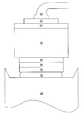
- FIG. 1schematically illustrates a conventional LED having an n-type SiC substrate 10 , an active region 12 comprising an n-GaN-based layer 14 and a p-GaN-based layer 16 grown on the substrate and patterned into a mesa.
- a metal p-electrode 18is deposited on and electrically coupled to the p-GaN layer 16 and a wire bond connection 28 is made to a bond pad 20 on the p-electrode 18 .
- An n-electrode 22 on and electrically coupled to the conductive substrateis attached to metallic submount 24 using a conductive epoxy 26 .
- the conductive epoxy 26usually silver epoxy
- the LEDis pressed into the epoxy 26 .
- the epoxyis then heat cured which causes it to harden, providing a stable and electrically conductive mount for the LED chip.
- Light generated in the active region 12is directed up and out of the device. However, a substantial amount of the generated light may be transmitted into the substrate and partially absorbed by the epoxy 26 .
- Flip-chip mounting of LEDsinvolves mounting the LED onto the submount substrate side up. Light is then extracted and emitted through the transparent substrate.
- Flip chip mountingmay be an especially desirable technique for mounting SiC-based LEDs. Since SiC has a higher index of refraction than GaN, light generated in the active region does not internally reflect (i.e. reflect back into the GaN-based layers) at the GaN/SiC interface.
- Flip chip mounting of SiC-based LEDsmay offer improved light extraction when employing certain chip-shaping techniques known in the art.
- Flip chip packaging of SiC LEDsmay have other benefits as well, such as improved heat extraction/dissipation, which may be desirable depending on the particular application for the chip.
- FIG. 2One problem with flip-chip mounting is illustrated in FIG. 2 . Namely, when a chip is flip-chip mounted on a conductive submount or package conventional techniques may not be possible. Conventionally, a conductive die attach material 26 , such as silver epoxy, is deposited on the chip and/or on the submount 24 , and the chip is pressed onto the submount 24 . This can cause the viscous conductive die attach material 26 to squeeze out and make contact with the n-type layers 14 and 10 in the device, thereby forming a Schottky diode connection that shunts the p-n junction in the active region with predictably undesirable results. Thus, new techniques may be needed for flip-chip mounting of LEDs.
- a conductive die attach material 26such as silver epoxy
- Embodiments of the present inventionprovide for mounting a light emitting device having a gallium nitride based light emitting region on a silicon carbide substrate in a flip-chip configuration by mounting an electrode of the gallium nitride based light emitting region to a submount utilizing a B-stage curable die epoxy.
- the electrodeis mounted to the submount by forming a predefined pattern of the B-stage curable die epoxy on the electrode, the predefined pattern covering only a predefined portion of the electrode.
- the electrode of the gallium nitride based light emitting regionis attached to the submount utilizing the predefined pattern of the B-stage curable die epoxy.
- the predefined pattern of B-stage curable die epoxymay be provided by applying the B-stage curable die epoxy to the electrode by screen printing.
- the screen printingprovides a resolution of application of the B-stage curable die epoxy of about 4 mils.
- the predefined pattern of B-stage curable die epoxymay also be provided by dispensing the B-stage epoxy onto desired locations of the electrode. Furthermore, the predefined pattern of B-stage curable die epoxy can be provided by coating the electrode with a B-stage epoxy and selectively removing B-stage epoxy from the electrode to provide the predefined pattern. The B-stage epoxy may be selectively removed by laser scribing the B-stage epoxy to selectively remove epoxy to provide the predefined pattern. If the B-stage epoxy is a photo-sensitive B-stage epoxy the B-stage epoxy may be selectively removed utilizing photolithography to provide the predefined pattern. The predefined pattern of B-stage curable die epoxy may also be provided by pin transferring the B-stage epoxy to locations on the electrode to provide the predefined pattern.
- forming a predefined pattern of B-stage curable die epoxyis followed by pre-curing the B-stage epoxy.
- the pre-curing of the B-stage epoxycan be provided by pre-curing the B-stage epoxy utilizing a temperature of from about 50 to about 150° C.
- the B-stage epoxycan be pre-cured utilizing a temperature of about 85° C.
- the electrode of the gallium nitride based light emitting regionmay be attached to the submount utilizing the predefined pattern of the B-stage curable die epoxy by placing the light emitting device on the submount and heating the B-stage epoxy to a final curing temperature so as to cause the B-stage epoxy to re-flow.
- the B-stage epoxymay be heated to a temperature of at least about 150° C.
- the predefined patternis a single nodule of B-stage epoxy on the electrode.
- the predefined patternmay also be a plurality of bumps of B-stage epoxy on the electrode.
- the predefined patternmay further be a plurality of lines of B-stage epoxy on the electrode.
- the predefined patterncould also be a criss-cross pattern of B-stage epoxy on the electrode.
- a light emitting device die having a mesa configuration on a substrate and an electrode on the mesais attached to a submount in a flip-chip configuration by forming predefined pattern of conductive die attach material on at least one of the electrode and the submount and mounting the light emitting device die to the submount.
- the predefined pattern of conductive die attach materialis selected so as to prevent the conductive die attach material from contacting sidewalls of the mesa or the substrate when the light emitting device die is mounted to the submount.
- the predefined pattern of conductive die attach materialmay provide a volume of die attach material that is less than a volume defined by an area of the electrode and a distance between the electrode and the submount.
- the predefined patternis a single nodule of conductive die attach material on the electrode.
- the predefined patternmay also be a plurality of bumps of conductive die attach material on the electrode.
- the predefined patternmay further be a plurality of lines of conductive die attach material on the electrode.
- the predefined patterncould also be a criss-cross pattern of conductive die attach material on the electrode.
- the conductive die attach materialis at least one of a B-stage curable die epoxy, a solder paste, a pattern of solder bumps, and/or a conductive polymer.
- the predefined patternmay be provided by forming a predefined pattern of solder paste by at least one of screen printing, dispensing and/or pin transferring.
- the conductive die attach materialis solder bumps
- the predefined patternmay be provided by forming a predefined pattern of solder bumps by at least one of dispensing a solder paste and reflowing, electroplating and/or dipping.
- the predefined patternmay be provided by forming a pattern of a B-stage curable-die epoxy and/or a conductive polymer by screen printing, dispensing, dispensing and reflowing, layering and laser scribing, photolithography and/or pin transferring methods.
- light emitting device die suitable for mounting on a submountincludes a conducting substrate, such as a silicon carbide substrate, a gallium nitride based active region on the silicon carbide substrate and a first electrode on the gallium nitride based active region opposite the substrate.
- a conducting substratesuch as a silicon carbide substrate, a gallium nitride based active region on the silicon carbide substrate and a first electrode on the gallium nitride based active region opposite the substrate.
- the first electrode and the gallium nitride based active regionform a mesa having sidewalls.
- a second electrodeis provided on the silicon carbide substrate opposite the gallium nitride active region.
- a predefined pattern of conductive die attach materialis provided on the first electrode opposite the gallium nitride active region that substantially prevents the conductive die attach material from contacting the sidewalls of the mesa and/or the substrate when the light emitting device die is mounted to the submount.
- the predefined pattern of conductive die attach materialmay provide a volume of die attach material that is less than a volume defined by an area of the first electrode and a distance between the first electrode and the submount.
- the predefined patternmay be a single nodule of conductive die attach material on the first electrode.
- the predefined patternmay also be a plurality of bumps of conductive die attach material on the first electrode.
- the predefined patterncould be a plurality of lines of conductive die attach material on the first electrode.
- the predefined patterncould also be a criss-cross pattern of conductive die attach material on the first electrode.
- the conductive die attach materialmay be a B-stage curable die epoxy, a solder paste, a pattern of solder bumps, and/or a conductive polymer.
- a submountmay also be provided.
- the first electrodeis mounted to the submount by the predefined pattern of conductive die attach material.
- Additional embodiments of the present inventionprovide a light emitting device die suitable for mounting on a submount that includes a substrate, such as a silicon carbide substrate, a gallium nitride based active region on the substrate and a first electrode on the nitride based active region opposite the substrate.
- the first electrode and the gallium nitride based active regionmay form a mesa having sidewalls.
- a second electrodemay be provided on the substrate opposite the gallium nitride active region.
- the B-stage conductive epoxyis provided on the first electrode opposite the gallium nitride active region.
- the B-stage conductive epoxymay be provided in a predefined pattern.
- the predefined pattern of B-stage conductive epoxymay provide a volume of B-stage conductive epoxy that is less than a volume defined by an area of the first electrode and a distance between the first electrode and the submount.
- the predefined patternmay be a single nodule of B-stage conductive epoxy on the first electrode.
- the predefined patterncould also be a plurality of bumps of B-stage conductive epoxy on the first electrode.
- the predefined patternmay further be a plurality of lines of B-stage conductive epoxy on the first electrode.
- the predefined patterncould also be a criss-cross pattern of B-stage conductive epoxy on the first electrode.
- a submountmay also be provided.
- the first electrodeis mounted to the submount by the B-stage conductive epoxy.
- a light emitting device dieincludes a gallium nitride based active region having at least one region of a first conductivity type and a first electrode electrically coupled to the gallium nitride based active region.
- a region of semiconductor material of a second conductivity typeis electrically coupled to the gallium nitride based active region.
- the second conductivity typeis opposite to the first conductivity type.
- a predefined pattern of conductive die attach materialis on the first electrode opposite the gallium nitride active region and configured to substantially prevent the conductive die attach material from contacting the region of semiconductor material of a second conductivity type when the light emitting device die is mounted to a submount.
- a second electrodemay also be provided on the region of semiconductor material of a second conductivity type.
- a substratemay also be provide and the gallium nitride based active region may be on the substrate.
- the first electrode and the second electrodemay be on opposite sides of the substrate or may be on the same side of the substrate.
- the substratemay be insulating or conductive. In certain embodiments of the present invention, the substrate is a silicon carbide substrate.
- FIG. 1is a schematic illustration of a conventional LED
- FIG. 2is a schematic illustration of a flip-chip mounted LED utilizing conventional techniques
- FIGS. 3A , 3 B, 3 C and 3 Dare illustrations of patterns of die attach material according to various embodiments of the present invention.
- FIG. 4is a flowchart illustrating operations according to embodiments of the present invention.
- FIG. 5is an illustration of an LED attached to a submount according to embodiments of the present invention.
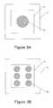
- FIG. 6is a planar view of an LED with a p-type electrode having die attach material bumps in a pattern according to embodiments of the present invention
- FIG. 7is a side view of the LED of FIG. 6 ;
- FIG. 8is a side view of the LED of FIGS. 6 and 7 after mounting to the submount.
- Embodiments of the present inventionprovide for connecting a light emitting device having a light emitting element, such as an LED die, to a submount or package in a flip-chip configuration using a die attach material that can be applied to an electrode of the light emitting device, such as the p-electrode, and/or the submount or package prior to packaging the light emitting device.
- the die attach materialcan be used to form a conductive attachment between the light emitting device and the submount without forming a parasitic diode that shunts the p-n diode of the device.
- the shunt diodemay be avoided by preventing the conductive adhesive from substantially flowing during curing.
- the shunt diodemay be avoided by preventing the conductive adhesive from contacting a region of the device of opposite conductivity type to that of the region to which the conductive adhesive provides a contact.
- the shunt diodemay be avoided by preventing the conductive adhesive from contacting an n-type region of the device. If the conductive adhesive provides a contact to the n-type contact of the device, the shunt diode may be avoided by preventing the conductive adhesive from contacting a p-type region of the device.
- the conductive adhesivemay facilitate heat extraction from the device when the device is mounted in a flip-chip configuration. Such heat extraction may be beneficial for high power devices, such as devices that may be suitable for use in white light applications.
- the present inventionis described herein primarily with reference to devices having contacts on opposite sides of the device, embodiments of the present invention may also be beneficial for devices having both contacts on the same side of the device.
- the conductive adhesivemay provided in a manner where the conductive adhesive of the contact do not form a shunt diode by contacting a regions of the device of opposite conductivity type of that to which the conductive adhesive makes contact.
- the conductive adhesive of the two contactsshould not contact each other.
- Embodiments of the present inventionare described herein with reference to a GaN based LED on an n-type SiC substrate 10 and having a n-type layer 14 , a p-type layer 16 and a p-electrode 18 electrically coupled to the p-type layer.
- the present inventionshould not be construed as limited to such structures.
- references herein to the conductive die attach material shorting to the n-type regions 10 and 14are provided for illustrative purposes only.
- references to shorting to the n-type regions 10 and 14may be considered as references to other layers in other device structures (for example to quantum well and/or barrier layers in a multi-quantum well device) where unintentional contact with the die attach material would result in impaired performance, reliability or other characteristics of the device.
- Light emitting devices for use in embodiments of the present inventionmay be gallium nitride based LEDs or lasers fabricated on a silicon carbide substrate such as those devices manufactured and sold by Cree, Inc. of Durham, N.C.
- the present inventionmay be suitable for use with LEDs and/or lasers as described in U.S. Pat. Nos.
- the light emitting devicesmay include a p-electrode that provides a reflecting layer to reflect light generated in the active region back through the device.
- Reflective p-electrodes and related structuresare described in U.S. patent application Ser. No. 10/057,82 entitled “LIGHT EMITTING DIODES INCLUDING SUBSTRATE MODIFICATIONS FOR LIGHT EXTRACTION AND MANUFACTURING METHODS THEREFOR” filed Jan. 25, 2002, which is hereby incorporated by reference as if set forth fully herein.
- the LEDs and/or lasersmay be configured to operate in a “flip-chip” configuration such that light emission occurs through the substrate.
- the substratemay be patterned so as to enhance light output of the devices as is described, for example, in U.S. Provisional Patent Application Ser. No. 60/307,235 filed Jul. 23, 2001 entitled “LIGHT EMITTING DIODES INCLUDING SUBSTRATE MODIFICATIONS FOR LIGHT EXTRACTION AND MANUFACTURING METHODS THEREFOR” and U.S. patent application Ser. No. 10/057,82 filed Jan. 25, 2002 entitled entitled “LIGHT EMITTING DIODES INCLUDING SUBSTRATE MODIFICATIONS FOR LIGHT EXTRACTION AND MANUFACTURING METHODS THEREFOR.”
- the die attach materialmay be provided in a pattern on the p-electrode of a gallium nitride based light emitting device formed on a silicon carbide substrate.
- the term patternmeans that the die attach material covers some, but not all, of the surface on which it is placed.
- the patternmay be selected so as to substantially prevent the conductive die attach material from flowing to the sidewalls of the gallium nitride device so as to short the active region of the device.
- the patternmay be selected to prevent the conductive adhesive from substantially flowing during curing/bonding. Examples of suitable patterns of conductive die attach material are shown in FIGS. 3A-3D . As seen in FIG.
- a single nodule of die attach material 30is provided on a p-electrode 18 of a light emitting device on the substrate 10 .
- FIG. 3Bshows die attach material 30 formed in an array of nodules on the p-electrode 18 .
- FIG. 3Cshows die attach material 30 formed in an array of lines on the p-electrode 18 .
- FIG. 3Dshows die attach material 30 formed in a criss-cross or “X” pattern on the p-electrode 18 .
- Other patternsmay be employed without departing from the invention.
- the pattern of conductive die attach materialprovides a volume of die attach material which is less than a volume defined by the area of the p-electrode of the light emitting device and the distance between the light emitting device and the submount.
- Suitable die attach materialsinclude a B-stage curable die epoxy (or a “B-stage epoxy”), a solder paste, a pattern of solder bumps, and/or a conductive polymer.
- Embodiments of the inventioninclude methods of applying a die attach material to an LED die or wafer and further include an LED die having deposited thereon a die attach material. Additional embodiments include methods of patterning a die attach material on an LED die or applying a patterned die attach material to an LED die or wafer, and further include the resulting LED die.
- the die attach materialmay comprise a standard B-stage epoxy.
- epoxiesare available commercially from, for example, Emerson Cumming, Ablestik, Dexter, Diemat and Epotek.
- Ablestik's RP333-3 epoxy, Dexter's BMI-519 epoxy and Emerson and Cumming's LA-9843-28 epoxyare suitable B-stage epoxies.
- the epoxyhas the following characteristics:
- the B-stage epoxyneed not be electrically conductive, and a separate electrically conductive path may be provided.
- the die attach materialmay comprise a conductive polymer such as CB028 manufactured by DuPont.
- a GaN based light emitting devicesuch as those described above, is fabricated on a SiC substrate (block 100 ).
- ohmic contactsare formed on opposite sides of the wafer.
- the waferis patterned into LEDs, for example, by etching to form a plurality of mesas.
- a passivation layeris formed to protect the epitaxial layers such as described in U.S. Provisional Patent Application Serial No. 60/352,941, filed Jan.
- the die attach materialmay contact the substrate, for example, at a portion where the substrate has been sawn or broken and, thereby form a shunt diode.
- the passivation layeris somehow damaged, for example at a region where the substrate is broken, a contact could unintentionally be made in such areas.
- the die attach materialis formed in a predefined pattern on the p-electrode of the LEDs (block 105 ). If a B-stage epoxy or conductive polymer is used, it may be deposited using any of the following techniques (or a combination of techniques, if desired):
- the B-stage epoxyOnce the B-stage epoxy has been deposited, it is pre-cured to cause it to solidify.
- Typical heat ranges for pre-curingare 50-150° C.
- the pre-curingoccurs at temperatures below 85° C. to avoid damaging other materials used in the manufacturing process such as a mounting tape.
- solder pastemay be used as the die attach material.
- Solder pastegenerally includes a solder metal or alloy such as Au/Ge, Pb/Sn, Au/Sn or In mixed together with solvents and/or binders to form a paste.
- Solder pastemay be applied by screen printing, dispensing or pin transferring as described above in connection with epoxies.
- pin transferring techniquesmay be used to provide a solder dot as the pattern of the die attach material. For example, a solder dot of about 0.2 mm formed by pin transfer techniques may be used to attach the device to the submount.
- the die attach materialmay comprise solder bumps formed on the p-electrode.
- Solder bumpsgenerally includes solder metal without binders or solvents, and may be deposited by, for example, dispensing a solder paste and subsequent reflow, electroplating and/or dipping.
- the waferis swan and/or sawn and broken using conventional techniques to separate the individual dies (block 110 ). Since the sawing may be done under a flow of de-ionized (DI) water, in some embodiments the conductive die attach material, such as the B-stage epoxy, is able to withstand water as well as the mechanical stress imparted from sawing and breaking. The individual die may then be secured onto adhesive tape rolls to facilitate automated packaging. Additionally, unitized groups of dies may be provided as described in U.S.
- Individual diesmay then be attached to a submount utilizing the conductive die attach material on the p-electrode (block 115 ).
- the diemay be set in place on the submount and heated to a final curing temperature (typically in excess of 150° C.). This causes the epoxy to re-flow and create a permanent connection between the LED chip and the submount.
- the conductive die attach materialutilized, the pattern of the material on the p-electrode and/or the pressure used during bonding, the conductive material does not flow onto the sidewalls of the mesa and/or the substrate of the device thereby creating a shunt diode in parallel with the active region of the device. A wirebond connection is then made to the n-electrode.
- FIG. 4illustrates embodiments of the present invention where the die attach material is provided on the p-electrode of the device
- the die attach materialmay be applied directly to the package or submount in a desired pattern or to both the submount and the p-electrode.
- the submountis heated to the final curing temperature and the LED chip is pressed onto the submount. Since a B-stage epoxy is used instead of the less viscous conventional epoxies, there is less likelihood of contacting the n-type layers of the active region of the device with the epoxy.
- FIG. 5illustrates an LED mounted in accordance with embodiments of the present invention.
- the die attach material epoxy 30is disposed between the p-electrode 18 and the submount 24 but does not contact the n-type layer 14 or the substrate 10 of the device.
- the volume of the die attach material 30is less than the volume defined by the area of the p-electrode 18 and the distance between the p-electrode 18 and the submount 24 .
- FIG. 6illustrates a substrate 10 and a p-electrode 18 of a light emitting device on which an array of bumps of conductive die attach material 30 have been formed, such as through deposition, patterning, plating and/or other techniques.
- FIG. 7illustrates the light emitting device of FIG. 6 in elevation. After deposition of the bumps 30 the LED is placed on a submount and the device is heated at a temperature sufficient to reflow the bumps 30 . In some embodiments, flux may also applied as part of the reflow process. The reflow temperature depends on the particular metal or alloy used.
- alloys containing a high percentage of Snmay have a melting point below 200° C., while alloys having a low percentage of Sn may have a melting point above 350° C.
- surface tensionkeeps the bumps from outflowing and wetting the n-type layer 14 or the substrate 10 of the LED.
- non-wettable patterns and/or solder damsmay be used to control outflow.
- FIG. 8illustrates an LED mounted in accordance with these embodiments of the present invention.
- the bumps of die attach material epoxy 30are disposed between the p-electrode 18 and the submount 24 but do not contact the n-type layer 14 or the substrate 10 of the device.
- the volume of the die attach material 30e.g. the solder bumps
- the volume of the die attach material 30is less than the volume defined by the area of the p-electrode 18 and the distance between the p-electrode 18 and the submount 24 . Therefore, no Schottky diode connection is made between the solder bumps and the n-type portions of the LED.
Landscapes
- Led Device Packages (AREA)
- Wire Bonding (AREA)
Abstract
Description
- B stage curable;
- Electrically conductive;
- Able to withstand water (during subsequent wafer sawing operations); and
- Sufficient physical strength to withstand subsequent processing operations (e.g. mounting and demounting from a tape).
- Screen printing. In these embodiments, the B-stage epoxy or polymer is applied to the p-electrodes by screen printing using automated vision control. Screen printing and machine vision systems are well known in the art and, therefore, will not be described further herein. A suitable screen printing machine for this application is the SPM screen printer manufactured by MPM corporation. If screen printing is used, the epoxy should be capable of being screen printed at appropriate dimensions. In some embodiments, the epoxy may be screen printable with a minimum feature size of about 4 mils.
- Dispensing. In these embodiments, the B-stage epoxy is dispensed directly from a source onto the desired locations on the wafer or submount. These embodiments may be used depending on the type of epoxy used and may include pin transfer, pneumatic dispensing and/or positive displacement dispensing via an auger or piston action.
- Layering and laser scribing. In these embodiments, the p-electrode side of the wafer is coated entirely with a B-stage epoxy, and laser scribing is used to selectively remove unwanted epoxy.
- Photolithography. In these embodiments, a photo-sensitive B-stage epoxy is applied to the p-electrode side of the wafer and photolithographic techniques are used to selectively remove unwanted epoxy.
Claims (35)
Priority Applications (12)
| Application Number | Priority Date | Filing Date | Title |
|---|---|---|---|
| US10/185,252US6888167B2 (en) | 2001-07-23 | 2002-06-27 | Flip-chip bonding of light emitting devices and light emitting devices suitable for flip-chip bonding |
| TW091116245ATW578276B (en) | 2001-07-23 | 2002-07-22 | Flip-chip bonding of light emitting devices and light emitting devices suitable for flip-chip bonding |
| AT02752483TATE527698T1 (en) | 2001-07-23 | 2002-07-22 | FLIP-CHIP BONDING OF LIGHT-EMITTING CHIPS |
| KR10-2004-7001063AKR20040029381A (en) | 2001-07-23 | 2002-07-22 | Flip chip bonding of light emitting devices and light emitting devices suitable for flip-chip bonding |
| PCT/US2002/023120WO2003010833A2 (en) | 2001-07-23 | 2002-07-22 | Flip chip bonding of light emitting devices and light emitting devices suitable for flip-chip bonding |
| CNB028186206ACN100392874C (en) | 2001-07-23 | 2002-07-22 | Flip chip bonding of light emitting device and light emitting device suitable for flip chip bonding |
| EP02752483AEP1417722B1 (en) | 2001-07-23 | 2002-07-22 | Flip-chip bonding of semiconductor light emitting chips |
| EP10179427.9AEP2262017A3 (en) | 2001-07-23 | 2002-07-22 | Flip-Chip bonding of light emitting devices and light emitting devices suitable for Flip-Chip bonding |
| JP2003516109AJP2005510043A (en) | 2001-07-23 | 2002-07-22 | Light emitting device suitable for flip chip bonding and flip chip bonding of light emitting devices |
| CA002454797ACA2454797A1 (en) | 2001-07-23 | 2002-07-22 | Flip-chip bonding of light emitting devices and light emitting devices suitable for flip-chip bonding |
| US10/920,101US7259033B2 (en) | 2001-07-23 | 2004-08-17 | Flip-chip bonding of light emitting devices |
| US11/772,419US7608860B2 (en) | 2001-07-23 | 2007-07-02 | Light emitting devices suitable for flip-chip bonding |
Applications Claiming Priority (2)
| Application Number | Priority Date | Filing Date | Title |
|---|---|---|---|
| US30731101P | 2001-07-23 | 2001-07-23 | |
| US10/185,252US6888167B2 (en) | 2001-07-23 | 2002-06-27 | Flip-chip bonding of light emitting devices and light emitting devices suitable for flip-chip bonding |
Related Child Applications (1)
| Application Number | Title | Priority Date | Filing Date |
|---|---|---|---|
| US10/920,101DivisionUS7259033B2 (en) | 2001-07-23 | 2004-08-17 | Flip-chip bonding of light emitting devices |
Publications (2)
| Publication Number | Publication Date |
|---|---|
| US20030045015A1 US20030045015A1 (en) | 2003-03-06 |
| US6888167B2true US6888167B2 (en) | 2005-05-03 |
Family
ID=26880972
Family Applications (3)
| Application Number | Title | Priority Date | Filing Date |
|---|---|---|---|
| US10/185,252Expired - LifetimeUS6888167B2 (en) | 2001-07-23 | 2002-06-27 | Flip-chip bonding of light emitting devices and light emitting devices suitable for flip-chip bonding |
| US10/920,101Expired - LifetimeUS7259033B2 (en) | 2001-07-23 | 2004-08-17 | Flip-chip bonding of light emitting devices |
| US11/772,419Expired - LifetimeUS7608860B2 (en) | 2001-07-23 | 2007-07-02 | Light emitting devices suitable for flip-chip bonding |
Family Applications After (2)
| Application Number | Title | Priority Date | Filing Date |
|---|---|---|---|
| US10/920,101Expired - LifetimeUS7259033B2 (en) | 2001-07-23 | 2004-08-17 | Flip-chip bonding of light emitting devices |
| US11/772,419Expired - LifetimeUS7608860B2 (en) | 2001-07-23 | 2007-07-02 | Light emitting devices suitable for flip-chip bonding |
Country Status (9)
| Country | Link |
|---|---|
| US (3) | US6888167B2 (en) |
| EP (2) | EP2262017A3 (en) |
| JP (1) | JP2005510043A (en) |
| KR (1) | KR20040029381A (en) |
| CN (1) | CN100392874C (en) |
| AT (1) | ATE527698T1 (en) |
| CA (1) | CA2454797A1 (en) |
| TW (1) | TW578276B (en) |
| WO (1) | WO2003010833A2 (en) |
Cited By (29)
| Publication number | Priority date | Publication date | Assignee | Title |
|---|---|---|---|---|
| US20070037307A1 (en)* | 2004-04-01 | 2007-02-15 | Matthew Donofrio | Method of Forming Three-Dimensional Features on Light Emitting Diodes for Improved Light Extraction |
| US20070063325A1 (en)* | 2005-09-22 | 2007-03-22 | Chun-Hung Lin | Chip package structure and bumping process |
| US20080014460A1 (en)* | 2003-04-01 | 2008-01-17 | Edmund Riedl | Method for the Multi-Stage Production of Diffusion Soldered Connections for Power Components Comprising Semiconductor Chips |
| US20080096365A1 (en)* | 2006-10-20 | 2008-04-24 | Cree, Inc. | Permanent wafer bonding using metal alloy preform discs |
| US20080121911A1 (en)* | 2006-11-28 | 2008-05-29 | Cree, Inc. | Optical preforms for solid state light emitting dice, and methods and systems for fabricating and assembling same |
| US20080283864A1 (en)* | 2007-05-16 | 2008-11-20 | Letoquin Ronan P | Single Crystal Phosphor Light Conversion Structures for Light Emitting Devices |
| US20090242897A1 (en)* | 2008-03-28 | 2009-10-01 | Cree, Inc. | Indium gallium nitride-based ohmic contact layers for gallium nitride-based devices |
| US20090315061A1 (en)* | 2008-06-24 | 2009-12-24 | Cree, Inc. | Methods of assembly for a semiconductor light emitting device package |
| US20110031502A1 (en)* | 2009-08-10 | 2011-02-10 | Cree, Inc. | Light emitting diodes including integrated backside reflector and die attach |
| US20110215355A1 (en)* | 2010-03-08 | 2011-09-08 | Van De Ven Antony P | Photonic crystal phosphor light conversion structures for light emitting devices |
| US20110233176A1 (en)* | 2010-03-25 | 2011-09-29 | Veeco Instruments, Inc. | Split laser scribe |
| WO2017059028A1 (en) | 2015-10-01 | 2017-04-06 | Cree, Inc. | Low optical loss flip chip solid state lighting device |
| US10297534B2 (en)* | 2014-12-11 | 2019-05-21 | Stmicroelectronics Pte Ltd | Integrated circuit (IC) package with a solder receiving area and associated methods |
| US10312224B2 (en) | 2016-04-12 | 2019-06-04 | Cree, Inc. | High density pixelated LED and devices and methods thereof |
| US10529773B2 (en) | 2018-02-14 | 2020-01-07 | Cree, Inc. | Solid state lighting devices with opposing emission directions |
| US10586787B2 (en) | 2007-01-22 | 2020-03-10 | Cree, Inc. | Illumination devices using externally interconnected arrays of light emitting devices, and methods of fabricating same |
| US10651357B2 (en) | 2017-08-03 | 2020-05-12 | Cree, Inc. | High density pixelated-led chips and chip array devices |
| US10734363B2 (en) | 2017-08-03 | 2020-08-04 | Cree, Inc. | High density pixelated-LED chips and chip array devices |
| US10879441B2 (en) | 2018-12-17 | 2020-12-29 | Cree, Inc. | Interconnects for light emitting diode chips |
| US10903265B2 (en) | 2018-12-21 | 2021-01-26 | Cree, Inc. | Pixelated-LED chips and chip array devices, and fabrication methods |
| US10985294B2 (en) | 2019-03-19 | 2021-04-20 | Creeled, Inc. | Contact structures for light emitting diode chips |
| US11031527B2 (en) | 2018-01-29 | 2021-06-08 | Creeled, Inc. | Reflective layers for light-emitting diodes |
| US11094848B2 (en) | 2019-08-16 | 2021-08-17 | Creeled, Inc. | Light-emitting diode chip structures |
| US11160148B2 (en) | 2017-06-13 | 2021-10-26 | Ideal Industries Lighting Llc | Adaptive area lamp |
| US11387389B2 (en) | 2018-01-29 | 2022-07-12 | Creeled, Inc. | Reflective layers for light-emitting diodes |
| US11437548B2 (en) | 2020-10-23 | 2022-09-06 | Creeled, Inc. | Pixelated-LED chips with inter-pixel underfill materials, and fabrication methods |
| US11792898B2 (en) | 2012-07-01 | 2023-10-17 | Ideal Industries Lighting Llc | Enhanced fixtures for area lighting |
| US11817526B2 (en) | 2019-10-29 | 2023-11-14 | Creeled, Inc. | Texturing for high density pixelated-LED chips and chip array devices |
| US11923481B2 (en) | 2018-01-29 | 2024-03-05 | Creeled, Inc. | Reflective layers for light-emitting diodes |
Families Citing this family (49)
| Publication number | Priority date | Publication date | Assignee | Title |
|---|---|---|---|---|
| US6747298B2 (en)* | 2001-07-23 | 2004-06-08 | Cree, Inc. | Collets for bonding of light emitting diodes having shaped substrates |
| CA2492249A1 (en) | 2002-07-22 | 2004-01-29 | Cree, Inc. | Light emitting diode including barrier layers and manufacturing methods therefor |
| US7009199B2 (en)* | 2002-10-22 | 2006-03-07 | Cree, Inc. | Electronic devices having a header and antiparallel connected light emitting diodes for producing light from AC current |
| DE60311678T2 (en)* | 2002-12-20 | 2007-11-22 | Cree, Inc. | METHOD FOR PRODUCING SEMICONDUCTOR DEVICES WITH MESASTRUCTURES AND MULTIPLE PASSIVATION LAYERS AND RELATED DEVICES |
| US20040188696A1 (en)* | 2003-03-28 | 2004-09-30 | Gelcore, Llc | LED power package |
| JP4766845B2 (en)* | 2003-07-25 | 2011-09-07 | シャープ株式会社 | Nitride-based compound semiconductor light-emitting device and method for manufacturing the same |
| JP2005203519A (en)* | 2004-01-14 | 2005-07-28 | Sumitomo Electric Ind Ltd | Semiconductor light emitting device |
| TWI230425B (en) | 2004-02-06 | 2005-04-01 | South Epitaxy Corp | Bumping process for light emitting diode |
| CN100347867C (en)* | 2004-02-26 | 2007-11-07 | 元砷光电科技股份有限公司 | Technique of solder ball for manufacutirng LED |
| US7462861B2 (en)* | 2004-04-28 | 2008-12-09 | Cree, Inc. | LED bonding structures and methods of fabricating LED bonding structures |
| US7329905B2 (en)* | 2004-06-30 | 2008-02-12 | Cree, Inc. | Chip-scale methods for packaging light emitting devices and chip-scale packaged light emitting devices |
| JP4644193B2 (en)* | 2004-07-12 | 2011-03-02 | ローム株式会社 | Semiconductor light emitting device |
| US7405093B2 (en)* | 2004-08-18 | 2008-07-29 | Cree, Inc. | Methods of assembly for a semiconductor light emitting device package |
| US7737459B2 (en)* | 2004-09-22 | 2010-06-15 | Cree, Inc. | High output group III nitride light emitting diodes |
| US7259402B2 (en)* | 2004-09-22 | 2007-08-21 | Cree, Inc. | High efficiency group III nitride-silicon carbide light emitting diode |
| US8513686B2 (en)* | 2004-09-22 | 2013-08-20 | Cree, Inc. | High output small area group III nitride LEDs |
| US8174037B2 (en)* | 2004-09-22 | 2012-05-08 | Cree, Inc. | High efficiency group III nitride LED with lenticular surface |
| US8288942B2 (en)* | 2004-12-28 | 2012-10-16 | Cree, Inc. | High efficacy white LED |
| TWI422044B (en)* | 2005-06-30 | 2014-01-01 | Cree Inc | Wafer-scale method for packaging light-emitting device and light-emitting device packaged by wafer scale |
| US20070015300A1 (en)* | 2005-07-15 | 2007-01-18 | Yu-Chuan Liu | Method for fabricating a light-emitting device |
| US7772604B2 (en) | 2006-01-05 | 2010-08-10 | Illumitex | Separate optical device for directing light from an LED |
| WO2007142946A2 (en) | 2006-05-31 | 2007-12-13 | Cree Led Lighting Solutions, Inc. | Lighting device and method of lighting |
| DE102006033873A1 (en)* | 2006-07-21 | 2008-01-24 | Patent-Treuhand-Gesellschaft für elektrische Glühlampen mbH | Radiation-emitting device with a plurality of radiation-emitting components and illumination device |
| US7635869B2 (en) | 2006-09-14 | 2009-12-22 | Lumination Llc | Support with recessed electrically conductive chip attachment material for flip-chip bonding a light emitting chip |
| WO2008042351A2 (en) | 2006-10-02 | 2008-04-10 | Illumitex, Inc. | Led system and method |
| EP2111640B1 (en)* | 2007-01-22 | 2019-05-08 | Cree, Inc. | Fault tolerant light emitter and method of fabricating the same |
| JP4987632B2 (en)* | 2007-08-30 | 2012-07-25 | 株式会社東芝 | Semiconductor device manufacturing method, submount manufacturing method, and electronic component |
| US8008707B2 (en) | 2007-12-14 | 2011-08-30 | Kabushiki Kaisha Toshiba | Nonvolatile semiconductor memory device provided with charge storage layer in memory cell |
| JP2011512037A (en) | 2008-02-08 | 2011-04-14 | イルミテックス, インコーポレイテッド | System and method for emitter layer shaping |
| TW201034256A (en) | 2008-12-11 | 2010-09-16 | Illumitex Inc | Systems and methods for packaging light-emitting diode devices |
| US20100248424A1 (en)* | 2009-03-27 | 2010-09-30 | Intellectual Business Machines Corporation | Self-Aligned Chip Stacking |
| US8585253B2 (en) | 2009-08-20 | 2013-11-19 | Illumitex, Inc. | System and method for color mixing lens array |
| US8449128B2 (en) | 2009-08-20 | 2013-05-28 | Illumitex, Inc. | System and method for a lens and phosphor layer |
| DE102010009717A1 (en) | 2010-03-01 | 2011-09-01 | Osram Opto Semiconductors Gmbh | LED chip |
| TWI407536B (en)* | 2010-12-10 | 2013-09-01 | Univ Nat Cheng Kung | Heat sink for semiconductor component manufacturing method |
| TW201230910A (en)* | 2011-01-11 | 2012-07-16 | Hon Hai Prec Ind Co Ltd | The method of manufacturing the LED lightbar and the equipment thereof |
| DE102011112000B4 (en) | 2011-08-31 | 2023-11-30 | OSRAM Opto Semiconductors Gesellschaft mit beschränkter Haftung | LED chip |
| US8426255B2 (en)* | 2011-09-14 | 2013-04-23 | Chipmos Technologies, Inc. | Chip package structure and method for manufacturing the same |
| US8933433B2 (en) | 2012-07-30 | 2015-01-13 | LuxVue Technology Corporation | Method and structure for receiving a micro device |
| US9484504B2 (en) | 2013-05-14 | 2016-11-01 | Apple Inc. | Micro LED with wavelength conversion layer |
| US9111464B2 (en) | 2013-06-18 | 2015-08-18 | LuxVue Technology Corporation | LED display with wavelength conversion layer |
| US9664641B2 (en) | 2013-07-29 | 2017-05-30 | Honeywell International Inc. | pH sensor with substrate or bonding layer configured to maintain piezoresistance of the ISFET die |
| US9671362B2 (en)* | 2013-07-29 | 2017-06-06 | Honeywell International Inc. | ph sensor with bonding agent disposed in a pattern |
| DE102015002176A1 (en)* | 2015-02-24 | 2016-08-25 | Jenoptik Laser Gmbh | Method of making a diode laser and diode laser |
| CN105921356B (en)* | 2016-05-20 | 2018-06-26 | 中国电子科技集团公司第十研究所 | Automatically chip attachment is back-shaped dips in rubber head |
| CN105903639B (en)* | 2016-05-20 | 2018-06-26 | 中国电子科技集团公司第十研究所 | Full-automatic chip attachment X-shaped point dips in rubber head |
| KR20170139924A (en) | 2016-06-10 | 2017-12-20 | 엘지전자 주식회사 | Transparent light-emitting diode film |
| US10312415B2 (en) | 2017-06-19 | 2019-06-04 | Microsoft Technology Licensing, Llc | Flexible electronic assembly with semiconductor die |
| CN109346405B (en)* | 2018-11-23 | 2021-12-03 | 江苏新广联科技股份有限公司 | Preparation method of GaN-based SBD flip chip |
Citations (38)
| Publication number | Priority date | Publication date | Assignee | Title |
|---|---|---|---|---|
| JPS559442A (en) | 1978-07-05 | 1980-01-23 | Matsushita Electric Ind Co Ltd | Light emission element and its manufacturing method |
| JPS55148477A (en) | 1979-05-08 | 1980-11-19 | Sanyo Electric Co Ltd | Fabricating method of light emitting diode |
| JPS5664484A (en) | 1979-10-30 | 1981-06-01 | Toshiba Corp | Led device |
| FR2610451A1 (en) | 1987-01-30 | 1988-08-05 | Radiotechnique Compelec | Opto-electronic device comprising at least one component mounted on a support |
| JPH02206136A (en) | 1989-02-06 | 1990-08-15 | Matsushita Electric Ind Co Ltd | Apparatus and method for die bonding |
| US5046161A (en) | 1988-02-23 | 1991-09-03 | Nec Corporation | Flip chip type semiconductor device |
| US5060027A (en) | 1988-08-11 | 1991-10-22 | Plessey Overseas Limited | Light emitting diode array with aligned solder bumps |
| JPH04152645A (en) | 1990-10-17 | 1992-05-26 | Toshiba Corp | Collet for die bonding use |
| US5117279A (en) | 1990-03-23 | 1992-05-26 | Motorola, Inc. | Semiconductor device having a low temperature uv-cured epoxy seal |
| US5118584A (en) | 1990-06-01 | 1992-06-02 | Eastman Kodak Company | Method of producing microbump circuits for flip chip mounting |
| JPH0529364A (en) | 1991-07-17 | 1993-02-05 | Sharp Corp | Bonding method and device for semiconductor device |
| EP0589524A2 (en) | 1992-09-25 | 1994-03-30 | Koninklijke Philips Electronics N.V. | Method of manufacturing an optoelectronic semiconductor device and optoelectronic semiconductor element suitable for use in such a method |
| US5438477A (en) | 1993-08-12 | 1995-08-01 | Lsi Logic Corporation | Die-attach technique for flip-chip style mounting of semiconductor dies |
| US5506451A (en) | 1993-12-27 | 1996-04-09 | Kabushiki Kaisha Toshiba | Flip-chip semiconductor devise having an electrode pad covered with non-metal member |
| JPH08172219A (en) | 1994-12-20 | 1996-07-02 | Sharp Corp | Multicolor LED element, LED display device using the multicolor LED element, and method for manufacturing multicolor LED element |
| US5672542A (en) | 1994-08-08 | 1997-09-30 | Hewlett Packard Company | Method of making solder balls by contained paste deposition |
| US5694482A (en) | 1994-11-08 | 1997-12-02 | Universal Instruments Corporation | System and method for locating solder bumps on semiconductor chips or chip carriers |
| EP0843365A2 (en) | 1992-08-20 | 1998-05-20 | Hewlett-Packard Company | Light source and technique for mounting light emitting diodes |
| US5760479A (en) | 1996-02-29 | 1998-06-02 | Texas Instruments Incorporated | Flip-chip die attachment for a high temperature die to substrate bond |
| US5773882A (en) | 1994-04-28 | 1998-06-30 | Kabushiki Kaisha Toshiba | Seminconductor package |
| US6057222A (en) | 1995-12-21 | 2000-05-02 | Siemens Aktiengesellschaft | Method for the production of flip-chip mounting-ready contacts of electrical components |
| EP1020935A2 (en) | 1999-01-11 | 2000-07-19 | Matsushita Electronics Corporation | Composite light-emitting device, semiconductor light-emitting unit and method for fabricating the unit |
| US6146984A (en) | 1999-10-08 | 2000-11-14 | Agilent Technologies Inc. | Method and structure for uniform height solder bumps on a semiconductor wafer |
| US6189772B1 (en) | 1998-08-31 | 2001-02-20 | Micron Technology, Inc. | Method of forming a solder ball |
| US6213789B1 (en) | 1999-12-15 | 2001-04-10 | Xerox Corporation | Method and apparatus for interconnecting devices using an adhesive |
| US6214733B1 (en) | 1999-11-17 | 2001-04-10 | Elo Technologies, Inc. | Process for lift off and handling of thin film materials |
| US6222279B1 (en) | 1995-03-20 | 2001-04-24 | Mcnc | Solder bump fabrication methods and structures including a titanium barrier layer |
| US6224690B1 (en) | 1995-12-22 | 2001-05-01 | International Business Machines Corporation | Flip-Chip interconnections using lead-free solders |
| WO2001047039A1 (en) | 1999-12-22 | 2001-06-28 | Lumileds Lighting, U.S., Llc | Method of making a iii-nitride light-emitting device with increased light generating capability |
| US20010006235A1 (en) | 1999-12-09 | 2001-07-05 | Masafumi Ozawa | Semiconductor light-emitting device and method of manufacturing the same and mounting plate |
| WO2001069978A1 (en) | 2000-03-17 | 2001-09-20 | Tridonicatco Gmbh & Co. Kg | Control of light-emitting diodes (leds) |
| US20010032985A1 (en) | 1999-12-22 | 2001-10-25 | Bhat Jerome C. | Multi-chip semiconductor LED assembly |
| US20020068373A1 (en)* | 2000-02-16 | 2002-06-06 | Nova Crystals, Inc. | Method for fabricating light emitting diodes |
| US20020139987A1 (en) | 2001-03-29 | 2002-10-03 | Collins William David | Monolithic series/parallel led arrays formed on highly resistive substrates |
| US6498355B1 (en) | 2001-10-09 | 2002-12-24 | Lumileds Lighting, U.S., Llc | High flux LED array |
| US6614056B1 (en)* | 1999-12-01 | 2003-09-02 | Cree Lighting Company | Scalable led with improved current spreading structures |
| US6657236B1 (en)* | 1999-12-03 | 2003-12-02 | Cree Lighting Company | Enhanced light extraction in LEDs through the use of internal and external optical elements |
| US20040026709A1 (en)* | 2000-04-26 | 2004-02-12 | Stefan Bader | Gan-based light emitting-diode chip and a method for producing a luminescent diode component |
Family Cites Families (31)
| Publication number | Priority date | Publication date | Assignee | Title |
|---|---|---|---|---|
| JPS559442B2 (en) | 1972-02-24 | 1980-03-10 | ||
| JPS57153479A (en)* | 1981-03-17 | 1982-09-22 | Matsushita Electric Ind Co Ltd | Nitride gallium light emitting element |
| US5027168A (en) | 1988-12-14 | 1991-06-25 | Cree Research, Inc. | Blue light emitting diode formed in silicon carbide |
| US4918497A (en) | 1988-12-14 | 1990-04-17 | Cree Research, Inc. | Blue light emitting diode formed in silicon carbide |
| EP0397911A1 (en)* | 1989-05-19 | 1990-11-22 | Siemens Aktiengesellschaft | Optoelectronic semiconductor device |
| US4966862A (en) | 1989-08-28 | 1990-10-30 | Cree Research, Inc. | Method of production of light emitting diodes |
| US5068708A (en)* | 1989-10-02 | 1991-11-26 | Advanced Micro Devices, Inc. | Ground plane for plastic encapsulated integrated circuit die packages |
| US5210051A (en) | 1990-03-27 | 1993-05-11 | Cree Research, Inc. | High efficiency light emitting diodes from bipolar gallium nitride |
| US5782102A (en) | 1992-04-24 | 1998-07-21 | Nippondenso Co., Ltd. | Automotive air conditioner having condenser and evaporator provided within air duct |
| US5416342A (en) | 1993-06-23 | 1995-05-16 | Cree Research, Inc. | Blue light-emitting diode with high external quantum efficiency |
| US5338944A (en) | 1993-09-22 | 1994-08-16 | Cree Research, Inc. | Blue light-emitting diode with degenerate junction structure |
| US5393993A (en) | 1993-12-13 | 1995-02-28 | Cree Research, Inc. | Buffer structure between silicon carbide and gallium nitride and resulting semiconductor devices |
| JP2540787B2 (en) | 1994-07-22 | 1996-10-09 | 日本電気株式会社 | Method for manufacturing semiconductor device |
| US5604135A (en) | 1994-08-12 | 1997-02-18 | Cree Research, Inc. | Method of forming green light emitting diode in silicon carbide |
| US5523589A (en) | 1994-09-20 | 1996-06-04 | Cree Research, Inc. | Vertical geometry light emitting diode with group III nitride active layer and extended lifetime |
| US5631190A (en) | 1994-10-07 | 1997-05-20 | Cree Research, Inc. | Method for producing high efficiency light-emitting diodes and resulting diode structures |
| JP2625654B2 (en)* | 1995-04-28 | 1997-07-02 | 日本電気株式会社 | Semiconductor device and manufacturing method thereof |
| US5739554A (en) | 1995-05-08 | 1998-04-14 | Cree Research, Inc. | Double heterojunction light emitting diode with gallium nitride active layer |
| US5836902A (en) | 1996-12-03 | 1998-11-17 | Gray; James C. | Splint |
| CN1300859C (en)* | 1997-01-31 | 2007-02-14 | 松下电器产业株式会社 | Light emitting element |
| JPH10256313A (en) | 1997-03-12 | 1998-09-25 | Dekusutaa Kk | Method of electrically bonding electronic element chip to mounting board |
| US6201262B1 (en) | 1997-10-07 | 2001-03-13 | Cree, Inc. | Group III nitride photonic devices on silicon carbide substrates with conductive buffer interlay structure |
| JPH11354848A (en)* | 1998-06-10 | 1999-12-24 | Matsushita Electron Corp | Semiconductor light emitting device |
| US6189208B1 (en)* | 1998-09-11 | 2001-02-20 | Polymer Flip Chip Corp. | Flip chip mounting technique |
| JP2000123957A (en) | 1998-10-14 | 2000-04-28 | Co-Op Chem Co Ltd | Electrodes of planar heating element |
| US6168972B1 (en)* | 1998-12-22 | 2001-01-02 | Fujitsu Limited | Flip chip pre-assembly underfill process |
| US6486499B1 (en)* | 1999-12-22 | 2002-11-26 | Lumileds Lighting U.S., Llc | III-nitride light-emitting device with increased light generating capability |
| US6400033B1 (en)* | 2000-06-01 | 2002-06-04 | Amkor Technology, Inc. | Reinforcing solder connections of electronic devices |
| US6506681B2 (en)* | 2000-12-06 | 2003-01-14 | Micron Technology, Inc. | Thin flip—chip method |
| US20020076854A1 (en)* | 2000-12-15 | 2002-06-20 | Pierce John L. | System, method and apparatus for constructing a semiconductor wafer-interposer using B-Stage laminates |
| US6455878B1 (en)* | 2001-05-15 | 2002-09-24 | Lumileds Lighting U.S., Llc | Semiconductor LED flip-chip having low refractive index underfill |
- 2002
- 2002-06-27USUS10/185,252patent/US6888167B2/ennot_activeExpired - Lifetime
- 2002-07-22ATAT02752483Tpatent/ATE527698T1/ennot_activeIP Right Cessation
- 2002-07-22KRKR10-2004-7001063Apatent/KR20040029381A/ennot_activeWithdrawn
- 2002-07-22TWTW091116245Apatent/TW578276B/ennot_activeIP Right Cessation
- 2002-07-22JPJP2003516109Apatent/JP2005510043A/enactivePending
- 2002-07-22WOPCT/US2002/023120patent/WO2003010833A2/enactiveApplication Filing
- 2002-07-22EPEP10179427.9Apatent/EP2262017A3/ennot_activeWithdrawn
- 2002-07-22CNCNB028186206Apatent/CN100392874C/ennot_activeExpired - Lifetime
- 2002-07-22EPEP02752483Apatent/EP1417722B1/ennot_activeExpired - Lifetime
- 2002-07-22CACA002454797Apatent/CA2454797A1/ennot_activeAbandoned
- 2004
- 2004-08-17USUS10/920,101patent/US7259033B2/ennot_activeExpired - Lifetime
- 2007
- 2007-07-02USUS11/772,419patent/US7608860B2/ennot_activeExpired - Lifetime
Patent Citations (38)
| Publication number | Priority date | Publication date | Assignee | Title |
|---|---|---|---|---|
| JPS559442A (en) | 1978-07-05 | 1980-01-23 | Matsushita Electric Ind Co Ltd | Light emission element and its manufacturing method |
| JPS55148477A (en) | 1979-05-08 | 1980-11-19 | Sanyo Electric Co Ltd | Fabricating method of light emitting diode |
| JPS5664484A (en) | 1979-10-30 | 1981-06-01 | Toshiba Corp | Led device |
| FR2610451A1 (en) | 1987-01-30 | 1988-08-05 | Radiotechnique Compelec | Opto-electronic device comprising at least one component mounted on a support |
| US5046161A (en) | 1988-02-23 | 1991-09-03 | Nec Corporation | Flip chip type semiconductor device |
| US5060027A (en) | 1988-08-11 | 1991-10-22 | Plessey Overseas Limited | Light emitting diode array with aligned solder bumps |
| JPH02206136A (en) | 1989-02-06 | 1990-08-15 | Matsushita Electric Ind Co Ltd | Apparatus and method for die bonding |
| US5117279A (en) | 1990-03-23 | 1992-05-26 | Motorola, Inc. | Semiconductor device having a low temperature uv-cured epoxy seal |
| US5118584A (en) | 1990-06-01 | 1992-06-02 | Eastman Kodak Company | Method of producing microbump circuits for flip chip mounting |
| JPH04152645A (en) | 1990-10-17 | 1992-05-26 | Toshiba Corp | Collet for die bonding use |
| JPH0529364A (en) | 1991-07-17 | 1993-02-05 | Sharp Corp | Bonding method and device for semiconductor device |
| EP0843365A2 (en) | 1992-08-20 | 1998-05-20 | Hewlett-Packard Company | Light source and technique for mounting light emitting diodes |
| EP0589524A2 (en) | 1992-09-25 | 1994-03-30 | Koninklijke Philips Electronics N.V. | Method of manufacturing an optoelectronic semiconductor device and optoelectronic semiconductor element suitable for use in such a method |
| US5438477A (en) | 1993-08-12 | 1995-08-01 | Lsi Logic Corporation | Die-attach technique for flip-chip style mounting of semiconductor dies |
| US5506451A (en) | 1993-12-27 | 1996-04-09 | Kabushiki Kaisha Toshiba | Flip-chip semiconductor devise having an electrode pad covered with non-metal member |
| US5773882A (en) | 1994-04-28 | 1998-06-30 | Kabushiki Kaisha Toshiba | Seminconductor package |
| US5672542A (en) | 1994-08-08 | 1997-09-30 | Hewlett Packard Company | Method of making solder balls by contained paste deposition |
| US5694482A (en) | 1994-11-08 | 1997-12-02 | Universal Instruments Corporation | System and method for locating solder bumps on semiconductor chips or chip carriers |
| JPH08172219A (en) | 1994-12-20 | 1996-07-02 | Sharp Corp | Multicolor LED element, LED display device using the multicolor LED element, and method for manufacturing multicolor LED element |
| US6222279B1 (en) | 1995-03-20 | 2001-04-24 | Mcnc | Solder bump fabrication methods and structures including a titanium barrier layer |
| US6057222A (en) | 1995-12-21 | 2000-05-02 | Siemens Aktiengesellschaft | Method for the production of flip-chip mounting-ready contacts of electrical components |
| US6224690B1 (en) | 1995-12-22 | 2001-05-01 | International Business Machines Corporation | Flip-Chip interconnections using lead-free solders |
| US5760479A (en) | 1996-02-29 | 1998-06-02 | Texas Instruments Incorporated | Flip-chip die attachment for a high temperature die to substrate bond |
| US6189772B1 (en) | 1998-08-31 | 2001-02-20 | Micron Technology, Inc. | Method of forming a solder ball |
| EP1020935A2 (en) | 1999-01-11 | 2000-07-19 | Matsushita Electronics Corporation | Composite light-emitting device, semiconductor light-emitting unit and method for fabricating the unit |
| US6146984A (en) | 1999-10-08 | 2000-11-14 | Agilent Technologies Inc. | Method and structure for uniform height solder bumps on a semiconductor wafer |
| US6214733B1 (en) | 1999-11-17 | 2001-04-10 | Elo Technologies, Inc. | Process for lift off and handling of thin film materials |
| US6614056B1 (en)* | 1999-12-01 | 2003-09-02 | Cree Lighting Company | Scalable led with improved current spreading structures |
| US6657236B1 (en)* | 1999-12-03 | 2003-12-02 | Cree Lighting Company | Enhanced light extraction in LEDs through the use of internal and external optical elements |
| US20010006235A1 (en) | 1999-12-09 | 2001-07-05 | Masafumi Ozawa | Semiconductor light-emitting device and method of manufacturing the same and mounting plate |
| US6213789B1 (en) | 1999-12-15 | 2001-04-10 | Xerox Corporation | Method and apparatus for interconnecting devices using an adhesive |
| WO2001047039A1 (en) | 1999-12-22 | 2001-06-28 | Lumileds Lighting, U.S., Llc | Method of making a iii-nitride light-emitting device with increased light generating capability |
| US20010032985A1 (en) | 1999-12-22 | 2001-10-25 | Bhat Jerome C. | Multi-chip semiconductor LED assembly |
| US20020068373A1 (en)* | 2000-02-16 | 2002-06-06 | Nova Crystals, Inc. | Method for fabricating light emitting diodes |
| WO2001069978A1 (en) | 2000-03-17 | 2001-09-20 | Tridonicatco Gmbh & Co. Kg | Control of light-emitting diodes (leds) |
| US20040026709A1 (en)* | 2000-04-26 | 2004-02-12 | Stefan Bader | Gan-based light emitting-diode chip and a method for producing a luminescent diode component |
| US20020139987A1 (en) | 2001-03-29 | 2002-10-03 | Collins William David | Monolithic series/parallel led arrays formed on highly resistive substrates |
| US6498355B1 (en) | 2001-10-09 | 2002-12-24 | Lumileds Lighting, U.S., Llc | High flux LED array |
Non-Patent Citations (6)
| Title |
|---|
| Abstract, "Light emitting diode holder for various electrical instrument LED mounting," A. N. Soldatenkov, Derwent Publications Ltd, London, GB, AN 1995-013018, Jul. 15, 1993, XP-002241924. |
| Abstract, "Thermosonic bonding: an alternative to area-array solder connections," Sa Yoon Kang, Teh-hua Ju, and Y. C. Lee, Electronic Components and Technology Conference, Florida, Jun. 2-4, 1993, XP-002241923. |
| B-Definitions: B Stage. http://www.isl-garnetuah.edu/Composites/b.html. Feb. 27, 2002. |
| Copy of International Search Report for PCT/US02/23067, dated Jun. 4, 2003. |
| Copy of International Search Report for PCT/US02/23120, dated May 16, 2003. |
| Epoxy Technology: Products-B Stage. http://www.epotek.com/b stage.html. Feb. 27, 2002. |
Cited By (57)
| Publication number | Priority date | Publication date | Assignee | Title |
|---|---|---|---|---|
| US20080014460A1 (en)* | 2003-04-01 | 2008-01-17 | Edmund Riedl | Method for the Multi-Stage Production of Diffusion Soldered Connections for Power Components Comprising Semiconductor Chips |
| US7851910B2 (en)* | 2003-04-01 | 2010-12-14 | Infineon Technologies Ag | Diffusion soldered semiconductor device |
| US20070037307A1 (en)* | 2004-04-01 | 2007-02-15 | Matthew Donofrio | Method of Forming Three-Dimensional Features on Light Emitting Diodes for Improved Light Extraction |
| US7384809B2 (en) | 2004-04-01 | 2008-06-10 | Cree, Inc. | Method of forming three-dimensional features on light emitting diodes for improved light extraction |
| US20080135866A1 (en)* | 2004-04-01 | 2008-06-12 | Cree, Inc. | Method of forming three dimensional features on light emitting diodes for improved light extraction |
| US20110068351A1 (en)* | 2004-04-01 | 2011-03-24 | Matthew Donofrio | Method of Forming Three Dimensional Features on Light Emitting Diodes for Improved Light Extraction |
| US7829906B2 (en) | 2004-04-01 | 2010-11-09 | Cree, Inc. | Three dimensional features on light emitting diodes for improved light extraction |
| US8263995B2 (en) | 2004-04-01 | 2012-09-11 | Cree, Inc. | Three dimensional features on light emitting diodes for improved light extraction |
| US20070063325A1 (en)* | 2005-09-22 | 2007-03-22 | Chun-Hung Lin | Chip package structure and bumping process |
| US20080096365A1 (en)* | 2006-10-20 | 2008-04-24 | Cree, Inc. | Permanent wafer bonding using metal alloy preform discs |
| US10873002B2 (en) | 2006-10-20 | 2020-12-22 | Cree, Inc. | Permanent wafer bonding using metal alloy preform discs |
| US20080121911A1 (en)* | 2006-11-28 | 2008-05-29 | Cree, Inc. | Optical preforms for solid state light emitting dice, and methods and systems for fabricating and assembling same |
| US10586787B2 (en) | 2007-01-22 | 2020-03-10 | Cree, Inc. | Illumination devices using externally interconnected arrays of light emitting devices, and methods of fabricating same |
| US12341137B2 (en) | 2007-01-22 | 2025-06-24 | Creeled, Inc. | Illumination devices using externally interconnected arrays of light emitting devices, and methods of fabricating same |
| US20080283864A1 (en)* | 2007-05-16 | 2008-11-20 | Letoquin Ronan P | Single Crystal Phosphor Light Conversion Structures for Light Emitting Devices |
| US7943924B2 (en) | 2008-03-28 | 2011-05-17 | Cree, Inc. | Indium gallium nitride-based Ohmic contact layers for gallium nitride-based devices |
| US20090242897A1 (en)* | 2008-03-28 | 2009-10-01 | Cree, Inc. | Indium gallium nitride-based ohmic contact layers for gallium nitride-based devices |
| US20100314640A1 (en)* | 2008-03-28 | 2010-12-16 | Cree, Inc. | Indium gallium nitride-based ohmic contact layers for gallium nitride-based devices |
| US7791101B2 (en) | 2008-03-28 | 2010-09-07 | Cree, Inc. | Indium gallium nitride-based ohmic contact layers for gallium nitride-based devices |
| US20090315061A1 (en)* | 2008-06-24 | 2009-12-24 | Cree, Inc. | Methods of assembly for a semiconductor light emitting device package |
| US9147812B2 (en) | 2008-06-24 | 2015-09-29 | Cree, Inc. | Methods of assembly for a semiconductor light emitting device package |
| US20110031502A1 (en)* | 2009-08-10 | 2011-02-10 | Cree, Inc. | Light emitting diodes including integrated backside reflector and die attach |
| US9437785B2 (en) | 2009-08-10 | 2016-09-06 | Cree, Inc. | Light emitting diodes including integrated backside reflector and die attach |
| US9991427B2 (en) | 2010-03-08 | 2018-06-05 | Cree, Inc. | Photonic crystal phosphor light conversion structures for light emitting devices |
| US20110215355A1 (en)* | 2010-03-08 | 2011-09-08 | Van De Ven Antony P | Photonic crystal phosphor light conversion structures for light emitting devices |
| US8519298B2 (en)* | 2010-03-25 | 2013-08-27 | Veeco Instruments, Inc. | Split laser scribe |
| US20110233176A1 (en)* | 2010-03-25 | 2011-09-29 | Veeco Instruments, Inc. | Split laser scribe |
| US11792898B2 (en) | 2012-07-01 | 2023-10-17 | Ideal Industries Lighting Llc | Enhanced fixtures for area lighting |
| US10297534B2 (en)* | 2014-12-11 | 2019-05-21 | Stmicroelectronics Pte Ltd | Integrated circuit (IC) package with a solder receiving area and associated methods |
| US10529652B2 (en) | 2014-12-11 | 2020-01-07 | Stmicroelectronics Pte Ltd | Integrated circuit (IC) package with a solder receiving area and associated methods |
| WO2017059028A1 (en) | 2015-10-01 | 2017-04-06 | Cree, Inc. | Low optical loss flip chip solid state lighting device |
| US10991861B2 (en) | 2015-10-01 | 2021-04-27 | Cree, Inc. | Low optical loss flip chip solid state lighting device |
| US10529696B2 (en) | 2016-04-12 | 2020-01-07 | Cree, Inc. | High density pixelated LED and devices and methods thereof |
| US10312224B2 (en) | 2016-04-12 | 2019-06-04 | Cree, Inc. | High density pixelated LED and devices and methods thereof |
| US10910352B2 (en) | 2016-04-12 | 2021-02-02 | Cree, Inc. | High density pixelated LED and devices and methods thereof |
| US11776938B2 (en) | 2016-04-12 | 2023-10-03 | Creeled, Inc. | High density pixelated LED and devices and methods thereof |
| US11387221B2 (en) | 2016-04-12 | 2022-07-12 | Creeled, Inc. | High density pixelated LED and devices and methods thereof |
| US11160148B2 (en) | 2017-06-13 | 2021-10-26 | Ideal Industries Lighting Llc | Adaptive area lamp |
| US11417635B2 (en) | 2017-08-03 | 2022-08-16 | Creeled, Inc. | High density pixelated-LED chips and chip array devices |
| US10734363B2 (en) | 2017-08-03 | 2020-08-04 | Cree, Inc. | High density pixelated-LED chips and chip array devices |
| US10651357B2 (en) | 2017-08-03 | 2020-05-12 | Cree, Inc. | High density pixelated-led chips and chip array devices |
| US12328980B2 (en) | 2018-01-29 | 2025-06-10 | Creeled, Inc. | Reflective layers for light-emitting diodes |
| US11923481B2 (en) | 2018-01-29 | 2024-03-05 | Creeled, Inc. | Reflective layers for light-emitting diodes |
| US11031527B2 (en) | 2018-01-29 | 2021-06-08 | Creeled, Inc. | Reflective layers for light-emitting diodes |
| US11387389B2 (en) | 2018-01-29 | 2022-07-12 | Creeled, Inc. | Reflective layers for light-emitting diodes |
| US10529773B2 (en) | 2018-02-14 | 2020-01-07 | Cree, Inc. | Solid state lighting devices with opposing emission directions |
| US11398591B2 (en) | 2018-12-17 | 2022-07-26 | Creeled, Inc. | Interconnects for light emitting diode chips |
| US11817537B2 (en) | 2018-12-17 | 2023-11-14 | Creeled, Inc. | Interconnects for light emitting diode chips |
| US10879441B2 (en) | 2018-12-17 | 2020-12-29 | Cree, Inc. | Interconnects for light emitting diode chips |
| US11664407B2 (en) | 2018-12-21 | 2023-05-30 | Creeled, Inc. | Pixelated-LED chips and chip array devices, and fabrication methods |
| US10903268B2 (en) | 2018-12-21 | 2021-01-26 | Cree, Inc. | Pixelated-LED chips and chip array devices, and fabrication methods |
| US10903265B2 (en) | 2018-12-21 | 2021-01-26 | Cree, Inc. | Pixelated-LED chips and chip array devices, and fabrication methods |
| US11545595B2 (en) | 2019-03-19 | 2023-01-03 | Creeled, Inc. | Contact structures for light emitting diode chips |
| US10985294B2 (en) | 2019-03-19 | 2021-04-20 | Creeled, Inc. | Contact structures for light emitting diode chips |
| US11094848B2 (en) | 2019-08-16 | 2021-08-17 | Creeled, Inc. | Light-emitting diode chip structures |
| US11817526B2 (en) | 2019-10-29 | 2023-11-14 | Creeled, Inc. | Texturing for high density pixelated-LED chips and chip array devices |
| US11437548B2 (en) | 2020-10-23 | 2022-09-06 | Creeled, Inc. | Pixelated-LED chips with inter-pixel underfill materials, and fabrication methods |
Also Published As
| Publication number | Publication date |
|---|---|
| US7259033B2 (en) | 2007-08-21 |
| EP1417722A2 (en) | 2004-05-12 |
| JP2005510043A (en) | 2005-04-14 |
| EP2262017A2 (en) | 2010-12-15 |
| US7608860B2 (en) | 2009-10-27 |
| EP1417722B1 (en) | 2011-10-05 |
| CN1557025A (en) | 2004-12-22 |
| CN100392874C (en) | 2008-06-04 |
| WO2003010833A3 (en) | 2004-03-11 |
| WO2003010833A2 (en) | 2003-02-06 |
| US20030045015A1 (en) | 2003-03-06 |
| TW578276B (en) | 2004-03-01 |
| ATE527698T1 (en) | 2011-10-15 |
| CA2454797A1 (en) | 2003-02-06 |
| KR20040029381A (en) | 2004-04-06 |
| EP2262017A3 (en) | 2017-01-04 |
| US20050017256A1 (en) | 2005-01-27 |
| US20070241360A1 (en) | 2007-10-18 |
Similar Documents
| Publication | Publication Date | Title |
|---|---|---|
| US6888167B2 (en) | Flip-chip bonding of light emitting devices and light emitting devices suitable for flip-chip bonding | |
| US7642121B2 (en) | LED bonding structures and methods of fabricating LED bonding structures | |
| US7875533B2 (en) | Package-integrated thin film LED | |
| EP2056363B1 (en) | Light emitting diode package and method for fabricating same | |
| US7329905B2 (en) | Chip-scale methods for packaging light emitting devices and chip-scale packaged light emitting devices | |
| KR100568269B1 (en) | Gallium nitride based light emitting diode for flip-chip bonding and manufacturing method thereof | |
| US20080142817A1 (en) | Chip-scale methods for packaging light emitting devices and chip-scale packaged light emitting devices | |
| JP4141549B2 (en) | Manufacturing method of semiconductor light emitting device | |
| US20240047606A1 (en) | Wafer level fabrication for multiple chip light-emitting devices |
Legal Events
| Date | Code | Title | Description |
|---|---|---|---|
| AS | Assignment | Owner name:CREE LIGHTING COMPANY, GEORGIA Free format text:ASSIGNMENT OF ASSIGNORS INTEREST;ASSIGNORS:BHARATHAN, JAYESH;RAFFETTO, MARK;REEL/FRAME:013479/0468 Effective date:20020905 Owner name:CREE MICROWAVE, INC., CALIFORNIA Free format text:ASSIGNMENT OF ASSIGNORS INTEREST;ASSIGNOR:MOHAMMED, ANWAR;REEL/FRAME:013476/0637 Effective date:20020920 Owner name:CREE, INC., NORTH CAROLINA Free format text:ASSIGNMENT OF ASSIGNORS INTEREST;ASSIGNORS:SLATER, DAVID B. JR.;EDMOND, JOHN;NEGLEY, GERALD H.;AND OTHERS;REEL/FRAME:013479/0462;SIGNING DATES FROM 20020830 TO 20020917 | |
| AS | Assignment | Owner name:CREE, INC., NORTH CAROLINA Free format text:ASSIGNMENT OF ASSIGNORS INTEREST;ASSIGNOR:CREE LIGHTING COMPANY;REEL/FRAME:014386/0286 Effective date:20020618 | |
| STCF | Information on status: patent grant | Free format text:PATENTED CASE | |
| AS | Assignment | Owner name:CREE MICROWAVE, LLC, NORTH CAROLINA Free format text:CONVERSION OF CORPORATION TO LIMITED LIABILITY COMPANY;ASSIGNOR:CREE MICROWAVE, INC.;REEL/FRAME:016624/0147 Effective date:20050623 | |
| FPAY | Fee payment | Year of fee payment:4 | |
| FPAY | Fee payment | Year of fee payment:8 | |
| FPAY | Fee payment | Year of fee payment:12 | |
| AS | Assignment | Owner name:CREE LED, INC., CALIFORNIA Free format text:ASSIGNMENT OF ASSIGNORS INTEREST;ASSIGNOR:CREE, INC.;REEL/FRAME:056012/0200 Effective date:20210301 | |
| AS | Assignment | Owner name:CITIZENS BANK, N.A., MASSACHUSETTS Free format text:SECURITY INTEREST;ASSIGNORS:SMART MODULAR TECHNOLOGIES, INC.;SMART HIGH RELIABILITY SOLUTIONS, LLC;SMART EMBEDDED COMPUTING, INC.;AND OTHERS;REEL/FRAME:058983/0001 Effective date:20220207 | |
| AS | Assignment | Owner name:SMART MODULAR TECHNOLOGIES, INC., CALIFORNIA Free format text:RELEASE OF PATENT SECURITY INTEREST RECORDED AT R/F 058983/0001;ASSIGNOR:CITIZENS BANK, N.A.;REEL/FRAME:071725/0207 Effective date:20250624 Owner name:SMART EMBEDDED COMPUTING, INC., ARIZONA Free format text:RELEASE OF PATENT SECURITY INTEREST RECORDED AT R/F 058983/0001;ASSIGNOR:CITIZENS BANK, N.A.;REEL/FRAME:071725/0207 Effective date:20250624 Owner name:SMART HIGH RELIABILITY SOLUTIONS LLC, CALIFORNIA Free format text:RELEASE OF PATENT SECURITY INTEREST RECORDED AT R/F 058983/0001;ASSIGNOR:CITIZENS BANK, N.A.;REEL/FRAME:071725/0207 Effective date:20250624 Owner name:CREELED, INC., CALIFORNIA Free format text:RELEASE OF PATENT SECURITY INTEREST RECORDED AT R/F 058983/0001;ASSIGNOR:CITIZENS BANK, N.A.;REEL/FRAME:071725/0207 Effective date:20250624 | |
| AS | Assignment | Owner name:CREELED, INC., CALIFORNIA Free format text:CORRECTIVE ASSIGNMENT TO CORRECT THE NAME OF THE ASSIGNEE PREVIOUSLY RECORDED ON REEL 56012 FRAME 200. ASSIGNOR(S) HEREBY CONFIRMS THE ASSIGNMENT;ASSIGNOR:CREE, INC.;REEL/FRAME:071874/0001 Effective date:20210301 |