US6887804B2 - Passivation processing over a memory link - Google Patents
Passivation processing over a memory linkDownload PDFInfo
- Publication number
- US6887804B2 US6887804B2US10/361,206US36120603AUS6887804B2US 6887804 B2US6887804 B2US 6887804B2US 36120603 AUS36120603 AUS 36120603AUS 6887804 B2US6887804 B2US 6887804B2
- Authority
- US
- United States
- Prior art keywords
- laser
- laser output
- link
- passivation layer
- output pulses
- Prior art date
- Legal status (The legal status is an assumption and is not a legal conclusion. Google has not performed a legal analysis and makes no representation as to the accuracy of the status listed.)
- Expired - Lifetime
Links
- 238000002161passivationMethods0.000titleclaimsabstractdescription153
- 238000012545processingMethods0.000titledescription30
- 238000000034methodMethods0.000claimsabstractdescription132
- 239000000463materialSubstances0.000claimsabstractdescription60
- 230000008569processEffects0.000claimsabstractdescription36
- 239000000758substrateSubstances0.000claimsdescription38
- 230000003287optical effectEffects0.000claimsdescription17
- PXHVJJICTQNCMI-UHFFFAOYSA-NNickelChemical compound[Ni]PXHVJJICTQNCMI-UHFFFAOYSA-N0.000claimsdescription16
- VYPSYNLAJGMNEJ-UHFFFAOYSA-NSilicium dioxideChemical compoundO=[Si]=OVYPSYNLAJGMNEJ-UHFFFAOYSA-N0.000claimsdescription16
- 229910052751metalInorganic materials0.000claimsdescription16
- 239000002184metalSubstances0.000claimsdescription16
- 239000011521glassSubstances0.000claimsdescription15
- -1disilicideChemical compound0.000claimsdescription13
- XUIMIQQOPSSXEZ-UHFFFAOYSA-NSiliconChemical compound[Si]XUIMIQQOPSSXEZ-UHFFFAOYSA-N0.000claimsdescription12
- 229910052710siliconInorganic materials0.000claimsdescription12
- 239000010703siliconSubstances0.000claimsdescription12
- BOTDANWDWHJENH-UHFFFAOYSA-NTetraethyl orthosilicateChemical compoundCCO[Si](OCC)(OCC)OCCBOTDANWDWHJENH-UHFFFAOYSA-N0.000claimsdescription10
- UMIVXZPTRXBADB-UHFFFAOYSA-NbenzocyclobuteneChemical compoundC1=CC=C2CCC2=C1UMIVXZPTRXBADB-UHFFFAOYSA-N0.000claimsdescription10
- 239000003989dielectric materialSubstances0.000claimsdescription10
- BASFCYQUMIYNBI-UHFFFAOYSA-NplatinumChemical compound[Pt]BASFCYQUMIYNBI-UHFFFAOYSA-N0.000claimsdescription10
- 229920003209poly(hydridosilsesquioxane)Polymers0.000claimsdescription10
- LLHKCFNBLRBOGN-UHFFFAOYSA-Npropylene glycol methyl ether acetateChemical compoundCOCC(C)OC(C)=OLLHKCFNBLRBOGN-UHFFFAOYSA-N0.000claimsdescription10
- 229910052759nickelInorganic materials0.000claimsdescription8
- 239000000377silicon dioxideSubstances0.000claimsdescription8
- 239000010936titaniumSubstances0.000claimsdescription8
- 229910052581Si3N4Inorganic materials0.000claimsdescription7
- 229910052782aluminiumInorganic materials0.000claimsdescription7
- XAGFODPZIPBFFR-UHFFFAOYSA-NaluminiumChemical compound[Al]XAGFODPZIPBFFR-UHFFFAOYSA-N0.000claimsdescription7
- 235000012239silicon dioxideNutrition0.000claimsdescription7
- HQVNEWCFYHHQES-UHFFFAOYSA-Nsilicon nitrideChemical compoundN12[Si]34N5[Si]62N3[Si]51N64HQVNEWCFYHHQES-UHFFFAOYSA-N0.000claimsdescription7
- 239000010937tungstenSubstances0.000claimsdescription7
- 229910052721tungstenInorganic materials0.000claimsdescription7
- RYGMFSIKBFXOCR-UHFFFAOYSA-NCopperChemical compound[Cu]RYGMFSIKBFXOCR-UHFFFAOYSA-N0.000claimsdescription6
- RTAQQCXQSZGOHL-UHFFFAOYSA-NTitaniumChemical compound[Ti]RTAQQCXQSZGOHL-UHFFFAOYSA-N0.000claimsdescription6
- 239000010949copperSubstances0.000claimsdescription6
- 229910052802copperInorganic materials0.000claimsdescription6
- 229910021420polycrystalline siliconInorganic materials0.000claimsdescription6
- 229910052719titaniumInorganic materials0.000claimsdescription6
- WFKWXMTUELFFGS-UHFFFAOYSA-NtungstenChemical compound[W]WFKWXMTUELFFGS-UHFFFAOYSA-N0.000claimsdescription6
- BPQQTUXANYXVAA-UHFFFAOYSA-NOrthosilicateChemical compound[O-][Si]([O-])([O-])[O-]BPQQTUXANYXVAA-UHFFFAOYSA-N0.000claimsdescription5
- PCHJSUWPFVWCPO-UHFFFAOYSA-NgoldChemical compound[Au]PCHJSUWPFVWCPO-UHFFFAOYSA-N0.000claimsdescription5
- 229910052737goldInorganic materials0.000claimsdescription5
- 239000010931goldSubstances0.000claimsdescription5
- 125000002496methyl groupChemical group[H]C([H])([H])*0.000claimsdescription5
- 229910052697platinumInorganic materials0.000claimsdescription5
- 229920000412polyarylenePolymers0.000claimsdescription5
- 229920005591polysiliconPolymers0.000claimsdescription5
- MZLGASXMSKOWSE-UHFFFAOYSA-Ntantalum nitrideChemical compound[Ta]#NMZLGASXMSKOWSE-UHFFFAOYSA-N0.000claimsdescription5
- 230000000977initiatory effectEffects0.000claimsdescription4
- WQJQOUPTWCFRMM-UHFFFAOYSA-Ntungsten disilicideChemical compound[Si]#[W]#[Si]WQJQOUPTWCFRMM-UHFFFAOYSA-N0.000claimsdescription4
- 229910021342tungsten silicideInorganic materials0.000claimsdescription4
- 238000009826distributionMethods0.000claimsdescription3
- 230000003993interactionEffects0.000claimsdescription3
- 238000000608laser ablationMethods0.000claimsdescription3
- 229910001092metal group alloyInorganic materials0.000claimsdescription2
- 150000004767nitridesChemical class0.000claimsdescription2
- 239000011253protective coatingSubstances0.000claimsdescription2
- RTZKZFJDLAIYFH-UHFFFAOYSA-NDiethyl etherChemical compoundCCOCCRTZKZFJDLAIYFH-UHFFFAOYSA-N0.000claims8
- 241000501667EtroplusSpecies0.000claims6
- 230000004044responseEffects0.000claims6
- 229940104869fluorosilicateDrugs0.000claims4
- NRTOMJZYCJJWKI-UHFFFAOYSA-NTitanium nitrideChemical compound[Ti]#NNRTOMJZYCJJWKI-UHFFFAOYSA-N0.000claims3
- 206010010144Completed suicideDiseases0.000claims2
- ATJFFYVFTNAWJD-UHFFFAOYSA-NTinChemical compound[Sn]ATJFFYVFTNAWJD-UHFFFAOYSA-N0.000claims1
- 238000003486chemical etchingMethods0.000abstractdescription6
- 238000005530etchingMethods0.000description12
- 238000007664blowingMethods0.000description9
- 238000010586diagramMethods0.000description8
- 238000006243chemical reactionMethods0.000description7
- 239000011295pitchSubstances0.000description6
- 238000000576coating methodMethods0.000description5
- 238000002679ablationMethods0.000description4
- 238000010521absorption reactionMethods0.000description4
- 239000011248coating agentSubstances0.000description4
- 229910052594sapphireInorganic materials0.000description4
- 239000010980sapphireSubstances0.000description4
- 235000012431wafersNutrition0.000description4
- 238000004519manufacturing processMethods0.000description3
- 230000005855radiationEffects0.000description3
- 239000000126substanceSubstances0.000description3
- 239000006096absorbing agentSubstances0.000description2
- 230000008901benefitEffects0.000description2
- 230000015556catabolic processEffects0.000description2
- 238000005336crackingMethods0.000description2
- 230000003247decreasing effectEffects0.000description2
- 230000007547defectEffects0.000description2
- 238000006073displacement reactionMethods0.000description2
- 230000000694effectsEffects0.000description2
- 150000002739metalsChemical class0.000description2
- 230000001902propagating effectEffects0.000description2
- 239000004065semiconductorSubstances0.000description2
- 241001270131Agaricus moelleriSpecies0.000description1
- 229910017502Nd:YVO4Inorganic materials0.000description1
- 229910052779NeodymiumInorganic materials0.000description1
- 206010035148PlagueDiseases0.000description1
- 101100107923Vitis labrusca AMAT geneProteins0.000description1
- 241000607479Yersinia pestisSpecies0.000description1
- 230000002411adverseEffects0.000description1
- 230000003667anti-reflective effectEffects0.000description1
- 238000003491arrayMethods0.000description1
- 230000006399behaviorEffects0.000description1
- 238000004140cleaningMethods0.000description1
- 229910052681coesiteInorganic materials0.000description1
- 239000000356contaminantSubstances0.000description1
- 230000008878couplingEffects0.000description1
- 238000010168coupling processMethods0.000description1
- 238000005859coupling reactionMethods0.000description1
- 229910052906cristobaliteInorganic materials0.000description1
- 239000013078crystalSubstances0.000description1
- 230000002950deficientEffects0.000description1
- 238000013461designMethods0.000description1
- 239000010432diamondSubstances0.000description1
- 150000002170ethersChemical class0.000description1
- 238000001704evaporationMethods0.000description1
- 238000004880explosionMethods0.000description1
- 239000002360explosiveSubstances0.000description1
- 239000000835fiberSubstances0.000description1
- 238000010304firingMethods0.000description1
- 230000006870functionEffects0.000description1
- 238000007429general methodMethods0.000description1
- 238000010438heat treatmentMethods0.000description1
- 230000001788irregularEffects0.000description1
- 230000007246mechanismEffects0.000description1
- 238000002844meltingMethods0.000description1
- 230000008018meltingEffects0.000description1
- 238000001465metallisationMethods0.000description1
- 239000000203mixtureSubstances0.000description1
- QEFYFXOXNSNQGX-UHFFFAOYSA-Nneodymium atomChemical compound[Nd]QEFYFXOXNSNQGX-UHFFFAOYSA-N0.000description1
- 229910052755nonmetalInorganic materials0.000description1
- 230000035515penetrationEffects0.000description1
- 238000000206photolithographyMethods0.000description1
- 238000006303photolysis reactionMethods0.000description1
- 229920002120photoresistant polymerPolymers0.000description1
- 239000003504photosensitizing agentSubstances0.000description1
- 238000001020plasma etchingMethods0.000description1
- 238000005086pumpingMethods0.000description1
- 230000003252repetitive effectEffects0.000description1
- 150000004760silicatesChemical class0.000description1
- 229910021332silicideInorganic materials0.000description1
- 238000001228spectrumMethods0.000description1
- 229910052682stishoviteInorganic materials0.000description1
- 230000035882stressEffects0.000description1
- 230000001360synchronised effectEffects0.000description1
- 239000013077target materialSubstances0.000description1
- 238000012360testing methodMethods0.000description1
- 230000008646thermal stressEffects0.000description1
- 229910052905tridymiteInorganic materials0.000description1
- 230000001960triggered effectEffects0.000description1
Images


Classifications
- H—ELECTRICITY
- H01—ELECTRIC ELEMENTS
- H01L—SEMICONDUCTOR DEVICES NOT COVERED BY CLASS H10
- H01L23/00—Details of semiconductor or other solid state devices
- H01L23/52—Arrangements for conducting electric current within the device in operation from one component to another, i.e. interconnections, e.g. wires, lead frames
- H01L23/522—Arrangements for conducting electric current within the device in operation from one component to another, i.e. interconnections, e.g. wires, lead frames including external interconnections consisting of a multilayer structure of conductive and insulating layers inseparably formed on the semiconductor body
- H01L23/525—Arrangements for conducting electric current within the device in operation from one component to another, i.e. interconnections, e.g. wires, lead frames including external interconnections consisting of a multilayer structure of conductive and insulating layers inseparably formed on the semiconductor body with adaptable interconnections
- H01L23/5256—Arrangements for conducting electric current within the device in operation from one component to another, i.e. interconnections, e.g. wires, lead frames including external interconnections consisting of a multilayer structure of conductive and insulating layers inseparably formed on the semiconductor body with adaptable interconnections comprising fuses, i.e. connections having their state changed from conductive to non-conductive
- H01L23/5258—Arrangements for conducting electric current within the device in operation from one component to another, i.e. interconnections, e.g. wires, lead frames including external interconnections consisting of a multilayer structure of conductive and insulating layers inseparably formed on the semiconductor body with adaptable interconnections comprising fuses, i.e. connections having their state changed from conductive to non-conductive the change of state resulting from the use of an external beam, e.g. laser beam or ion beam
- B—PERFORMING OPERATIONS; TRANSPORTING
- B23—MACHINE TOOLS; METAL-WORKING NOT OTHERWISE PROVIDED FOR
- B23K—SOLDERING OR UNSOLDERING; WELDING; CLADDING OR PLATING BY SOLDERING OR WELDING; CUTTING BY APPLYING HEAT LOCALLY, e.g. FLAME CUTTING; WORKING BY LASER BEAM
- B23K26/00—Working by laser beam, e.g. welding, cutting or boring
- B23K26/02—Positioning or observing the workpiece, e.g. with respect to the point of impact; Aligning, aiming or focusing the laser beam
- B23K26/04—Automatically aligning, aiming or focusing the laser beam, e.g. using the back-scattered light
- B23K26/042—Automatically aligning the laser beam
- B23K26/043—Automatically aligning the laser beam along the beam path, i.e. alignment of laser beam axis relative to laser beam apparatus
- B—PERFORMING OPERATIONS; TRANSPORTING
- B23—MACHINE TOOLS; METAL-WORKING NOT OTHERWISE PROVIDED FOR
- B23K—SOLDERING OR UNSOLDERING; WELDING; CLADDING OR PLATING BY SOLDERING OR WELDING; CUTTING BY APPLYING HEAT LOCALLY, e.g. FLAME CUTTING; WORKING BY LASER BEAM
- B23K26/00—Working by laser beam, e.g. welding, cutting or boring
- B23K26/02—Positioning or observing the workpiece, e.g. with respect to the point of impact; Aligning, aiming or focusing the laser beam
- B23K26/06—Shaping the laser beam, e.g. by masks or multi-focusing
- B23K26/0604—Shaping the laser beam, e.g. by masks or multi-focusing by a combination of beams
- B23K26/0613—Shaping the laser beam, e.g. by masks or multi-focusing by a combination of beams having a common axis
- B—PERFORMING OPERATIONS; TRANSPORTING
- B23—MACHINE TOOLS; METAL-WORKING NOT OTHERWISE PROVIDED FOR
- B23K—SOLDERING OR UNSOLDERING; WELDING; CLADDING OR PLATING BY SOLDERING OR WELDING; CUTTING BY APPLYING HEAT LOCALLY, e.g. FLAME CUTTING; WORKING BY LASER BEAM
- B23K26/00—Working by laser beam, e.g. welding, cutting or boring
- B23K26/02—Positioning or observing the workpiece, e.g. with respect to the point of impact; Aligning, aiming or focusing the laser beam
- B23K26/06—Shaping the laser beam, e.g. by masks or multi-focusing
- B23K26/062—Shaping the laser beam, e.g. by masks or multi-focusing by direct control of the laser beam
- B23K26/0622—Shaping the laser beam, e.g. by masks or multi-focusing by direct control of the laser beam by shaping pulses
- H—ELECTRICITY
- H01—ELECTRIC ELEMENTS
- H01L—SEMICONDUCTOR DEVICES NOT COVERED BY CLASS H10
- H01L2924/00—Indexing scheme for arrangements or methods for connecting or disconnecting semiconductor or solid-state bodies as covered by H01L24/00
- H01L2924/0001—Technical content checked by a classifier
- H01L2924/0002—Not covered by any one of groups H01L24/00, H01L24/00 and H01L2224/00
- H—ELECTRICITY
- H01—ELECTRIC ELEMENTS
- H01L—SEMICONDUCTOR DEVICES NOT COVERED BY CLASS H10
- H01L2924/00—Indexing scheme for arrangements or methods for connecting or disconnecting semiconductor or solid-state bodies as covered by H01L24/00
- H01L2924/095—Indexing scheme for arrangements or methods for connecting or disconnecting semiconductor or solid-state bodies as covered by H01L24/00 with a principal constituent of the material being a combination of two or more materials provided in the groups H01L2924/013 - H01L2924/0715
- H01L2924/097—Glass-ceramics, e.g. devitrified glass
- H01L2924/09701—Low temperature co-fired ceramic [LTCC]
- Y—GENERAL TAGGING OF NEW TECHNOLOGICAL DEVELOPMENTS; GENERAL TAGGING OF CROSS-SECTIONAL TECHNOLOGIES SPANNING OVER SEVERAL SECTIONS OF THE IPC; TECHNICAL SUBJECTS COVERED BY FORMER USPC CROSS-REFERENCE ART COLLECTIONS [XRACs] AND DIGESTS
- Y10—TECHNICAL SUBJECTS COVERED BY FORMER USPC
- Y10S—TECHNICAL SUBJECTS COVERED BY FORMER USPC CROSS-REFERENCE ART COLLECTIONS [XRACs] AND DIGESTS
- Y10S438/00—Semiconductor device manufacturing: process
- Y10S438/94—Laser ablative material removal
Definitions
- the present inventionrelates to processing of memory or other IC links and, in particular, to a laser system and method employing a one or more fast laser pulses to remove the passivation over an IC link on-the-fly so that it can be subsequently etched.
- FIGS. 1 , 2 A, and 2 Bshow repetitive electronic circuits 10 of an IC device or work piece 12 that are commonly fabricated in rows or columns to include multiple iterations of redundant circuit elements 14 , such as spare rows 16 and columns 18 of memory cells 20 .
- circuits 10are also designed to include particular laser severable conductive links 22 between electrical contacts 24 that can be removed to disconnect a defective memory cell 20 , for example, and substitute a replacement redundant cell 26 in a memory device such as a DRAM, an SRAM, or an embedded memory. Similar techniques are also used to sever links 22 to program a logic product, gate arrays, or ASICs.
- Links 22are about 0.3-2 microns ( ⁇ m) thick and are designed with conventional link widths 28 of about 0.4-2.5 ⁇ m, link lengths 30 , and element-to-element pitches (center-to-center spacings) 32 of about 2-8 ⁇ m from adjacent circuit structures or elements 34 , such as link structures 36 .
- link materialshave been polysilicon and like compositions
- memory manufacturershave more recently adopted a variety of more conductive metallic link materials that may include, but are not limited to, aluminum, copper, gold, nickel, titanium, tungsten, platinum, as well as other metals, metal alloys, metal nitrides such as titanium or tantalum nitride, metal silicides such as tungsten silicide, or other metal-like materials.
- Circuits 10 , circuit elements 14 , or cells 20are tested for defects, the locations of which may be mapped into a database or program.
- Traditional 1.047 ⁇ m or 1.064 ⁇ m infrared (IR) laser wavelengthshave been employed for more than 20 years to explosively remove conductive links 22 .
- Conventional memory link processing systemsfocus a single pulse of laser output having a pulse width of about 4 to 30 nanoseconds (ns) at a selected link 22 .
- FIGS. 2A and 2Bshow a laser spot 38 of spot size (area or diameter) 40 impinging a link structure 36 composed of a polysilicon or metal link 22 positioned above a silicon substrate 42 and between component layers of a passivation layer stack including an overlying passivation layer 44 (shown in FIG.
- the links 22are typically processed “on-the-fly” such that the beam positioning system does not have to stop moving when a laser pulse is fired at a selected link 22 , with each link 22 being processed by a single laser pulse.
- the on-the-fly processfacilitates a very high link-processing throughput, such as processing several tens of thousands of links 22 per second.
- FIG. 2Cis .a fragmentary cross-sectional side view of the link structure of FIG. 2B after the link 22 is removed by the prior art laser pulse.
- Sun et al. in U.S. Pat. No. 5,265,114 and U.S. Pat. No. 5,473,624proposed using a single 9 to 25 ns laser pulse at a longer laser wavelength, such as 1.3 ⁇ m, to process memory links 22 on silicon wafers.
- a longer laser wavelengthsuch as 1.3 ⁇ m
- the laser energy absorption contrast between the link material and silicon substrate 20is much larger than that at the traditional 1 ⁇ m laser wavelengths.
- the much wider laser processing window and better processing quality afforded by this techniquehas been used in the industry for about five years with great success.
- the 1 ⁇ m and 1.3 ⁇ m laser wavelengthshave disadvantages however.
- the energy coupling efficiency of such IR laser beams 12 into a highly electrically conductive metallic link 22is relatively poor; and the practical achievable spot size 40 of an IR laser beam for link severing is relatively large and limits the critical dimensions of link width 28 , link length 30 between contacts 24 , and link pitch 32 .
- This conventional laser link processingrelies on heating, melting, and evaporating link 22 , and creating a mechanical stress build-up to explosively open overlying passivation layer 44 with a single laser pulse. Such a conventional link processing laser pulse creates a large heat affected zone (HAZ) that could deteriorate the quality of the device that includes the severed link.
- HAZheat affected zone
- U.S. Pat. No. 6,057,180 of Sun et al.describes a method of using ultraviolet (UV) laser output to sever links with the benefit of a smaller beam spot size.
- UVultraviolet
- removal of the link itself by such a UV laser pulseentails careful consideration of the underlying passivation structure and material to protect the underlying passivation and silicon wafer from being damaged by the UV laser pulse.
- U.S. Pat. No. 5,329,152 of Janai et al.describes coating a metal layer with a laser absorbing resist material (and an anti-reflective material), blowing away the coatings with a high-powered YAG, excimer, or pulsed laser diode with fluences of 0.2-10 J/cm 2 at a 350-nm wavelength, and then etching the uncovered metal with a chemical or plasma etch process.
- Janaidescribes using laser pulses that travel through a resist material so that the laser pulses can react with the underlying metal and integrate it into the resist material to make the resist material etchable along with the metal (and/or partially blowing away the resist material).
- U.S. Pat. No. 5,236,551 of Panteaches providing metalization portions, covering them with a photoabsorptive polymeric dielectric, ablating the dielectric to uncover portions of the metal, etching the metal, and then coating the resulting surface with a polymeric dielectric.
- Pandiscloses only excimer lasers having wavelengths of less than 400 nm and relies on a sufficiently large energy fluence per pulse (10 mJ/cm 2 to 350 mJ/cm 2 ) to overcome the ablative photodecomposition threshold of the polymeric dielectric.
- U.S. Pat. No. 6,025,256 of Swenson et al.describes methods of using ultraviolet (UV) laser output to expose or ablate an etch protection layer, such as a resist or photoresist, coated over a link that may also have an overlying passivation material, to permit link removal (and removal of the overlying passivation material) by different material removal mechanisms, such as by chemical etching.
- UVultraviolet
- expose and etch removal techniquesemploy additional coating steps and additional developing and/or etching steps. The additional steps typically entail sending the wafer back to the front end of the manufacturing process for extra step(s).
- U.S. Pat. No. 5,656,186 of Mourou et al.discloses a general method of laser induced breakdown and ablation at several wavelengths by high repetition rate ultrafast laser pulses, typically shorter than 10 ps, and demonstrates creation of machined feature sizes that are smaller than the diffraction limited spot size.
- U.S. Pat. No. 5,208,437 of Miyauchi et al.discloses a method of using a single “Gaussian”-shaped pulse of a subnanosecond pulse width to process a link.
- U.S. Pat. No. 5,742,634 of Rieger et al.discloses a simultaneously Q-switched and mode-locked neodymium (Nd) laser device with diode pumping.
- the laseremits a series of pulses each having a duration time of 60 to 300 picoseconds (ps), under an envelope of a time duration of 100 ns.
- Another object of the inventionis to process the passivation layer above a link with a set of one or more low energy laser pulses.
- a further object of the inventionis to provide a method and apparatus for employing a much smaller laser beam spot size for link processing.
- Yet another object of the inventionis to deliver such sets of laser pulses to process the passivation layer on-the-fly.
- Still another object of the inventionis to avoid or minimize substrate damage and undesirable damage to the passivation structure.
- Still another object of the inventionis to avoid numerous extra processing steps while removing links with an alternative method to that of explosive laser blowing.
- a burst of ultrashort laser pulsesis employed to sever a conductive link in a substantially nonthermal manner that offers a wider processing window, eliminates undesirable HAZ effects, and achieves superior severed link quality.
- the duration of the burstis preferably in the range of 10 ns to 500 ns; and the pulse width of each laser pulse within the burst is generally shorter than 25 ps, preferably shorter than or equal to 10 ps, and most preferably about 10 ps to 100 fs or shorter.
- the burstcan be treated as a single “pulse” by conventional laser positioning systems to perform on-the-fly link removal without stopping whenever the laser system fires a burst of laser pulses at each selected link.
- the present inventionemploys laser output including set of one or more laser pulses, each with a laser pulse energy in a very safe range, to remove or “open” a target area of passivation layer 44 overlying a target IC link 22 such that the target link 22 is exposed and then can be etched by a separate process and such that the passivation layer 46 and silicon wafer 42 underlying the link 22 are not subjected to the amount of laser output energy used in a traditional link-processing technique.
- the pulse width of each laser pulse within the setis generally shorter than 30 ns, preferably in the range of 0.05 ps to 5 ns, and more preferably shorter than 10 ps.
- Each laser pulse within the sethas an energy or peak power per pulse that is less than the damage threshold for the substrate 42 supporting the link structure.
- the number of laser pulses in the setis controlled such that the laser output cleans off the bottom of the passivation layer 44 , but leaves at least some of the link 22 such that the underlying passivation layer 46 and the substrate 42 are not subjected to the laser energy induced damage and are completely intact.
- the duration of a set having at least one laser pulseis shorter than 1,000 ns, more preferably shorter than 500 ns, and most preferably shorter than 300 ns, and preferably in the range of 5 to 300 ns. Because the whole duration of the set is shorter than 1,000 ns, the set is considered to be a single “pulse” by a traditional link-severing laser positioning system. This practice does not, therefore, entail either a long dwell time or separate duplicative scanning passes of repositioning and refiring at each selected link that would effectively reduce the throughput by factor of about two or more.
- the laser spot of each of the pulses in the setencompasses the link width and the displacement between the laser spots of each pulse is less than the positioning accuracy of a typical positioning system, which is typically + ⁇ 0.05 to 0.2 ⁇ m.
- the laser systemcan still process the target areas of the passivation layer 44 overlying the target links 22 on-the-fly, i.e. the positioning system does not have to stop moving when the laser system fires a set of laser pulses at a target area of passivation layer 44 over each selected link 22 .
- Chemical etching of the links 22is also relatively indifferent to variations in the link structures 36 from work piece 12 to work piece 12 , such as the widths 28 and thicknesses of the links 22 , whereas conventional link processing parameters should be tailored to suit particular link structure characteristics.
- the chemical etching of the links 22entails only a single extra process step that can be performed locally and/or in-line such that the work pieces 12 need not be sent back to the front end of the processing line to undergo the etching step.
- a continuous wave (CW) mode-locked laser at high laser pulse repetition rate, followed by optical gate and an amplifiergenerates sets having one or more ultrashort laser pulses that are preferably from about 100 fs to about 10 ps.
- a Q-switched and CW mode-locked lasergenerates sets having ultrashort laser pulses that are preferably from about 100 fs to about 10 ps. Because each laser pulse within the set is ultrashort, its interaction with the target materials (passivation layers and metallic link) is substantially not thermal. Each laser pulse breaks off a thin sublayer of about 100-2,000 ⁇ of material, depending on the laser energy or peak power, laser wavelength, and type of material, until the passivation layer 44 over the link 22 is removed.
- This substantially nonthermal processmay mitigate certain irregular and inconsistent link processing quality associated with thermal-stress explosion behavior of passivation layers 44 of links 22 with widths narrower than about 1 ⁇ m or links 22 thicker (depthwise) than about 1 ⁇ m.
- the most common ultrashort-pulse laser sourceemits at a wavelength of about 800 nm and facilitates delivery of a small-sized laser spot. Thus, the process may facilitate greater circuit density.
- the setshave one or more laser pulses that are preferably from about 25 ps to about 20 ns or 30 ns.
- These sets of laser pulsescan be generated from a CW mode-locked laser system including an optical gate and an optional down stream amplifier or from two or more synchronized but offset lasers that share a portion of an optical path.
- FIG. 1is a schematic diagram of a portion of a DRAM showing the redundant layout of and programmable links in a spare row of generic circuit cells.
- FIG. 2 A and FIG. 2 A 1are fragmentary cross-sectional side views of a conventional, large semiconductor link structures, respectively with and without an underlying passivation layer, receiving a laser pulse characterized by a prior art pulse parameters.
- FIG. 2Bis a fragmentary top view of the link structure and the laser pulse of FIG. 2A , together with an adjacent circuit structure.
- FIG. 2Cis a fragmentary cross-sectional side view of the link structure of FIG. 2B after the link is removed by the prior art laser pulse.
- FIG. 3Ais a fragmentary cross-sectional side view of a target structure, covered by a passivation layer, receiving a laser output characterized by laser output parameters in accordance with the present invention.
- FIG. 3 Bis a fragmentary cross-sectional side view of the target structure of FIG. 3A subsequent to a passivation-removing laser processing step.
- FIG. 3Cis a fragmentary cross-sectional side view of the target structure of FIG. 3B subsequent to an etch processing step.
- FIG. 4shows a power versus time graph of exemplary sets of constant amplitude laser pulses employed to remove passivation material over links in accordance with the present invention.
- FIG. 5shows a power versus time graph of alternative exemplary sets of modulated amplitude laser pulses employed to remove passivation material over links in accordance with the present invention.
- FIG. 6shows a power versus time graph of other alternative exemplary sets of modulated amplitude laser pulses employed to remove passivation material over links in accordance with the present invention.
- FIG. 7is a partly schematic, simplified diagram of an embodiment of an exemplary green laser system including a work piece positioner that cooperates with a laser processing control system for practicing the method of the present invention.
- FIG. 8is a simplified schematic diagram of one laser configuration that can be employed to implement the present invention.
- FIG. 9is a simplified schematic diagram of an alternative embodiment of a laser configuration that can be employed to implement the present invention.
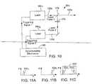
- FIG. 10is a simplified schematic diagram of an alternative embodiment of a laser system that employs two or more lasers to implement the present invention.
- FIGS. 11A-11Cshow respective power versus time graphs of exemplary laser pulses propagating along separate optical paths of the laser system shown in FIG. 10 .
- FIGS. 3A , 3 B, and 3 Care fragmentary cross-sectional side views of target structure 56 undergoing sequential stages of target processing in accordance with the present invention.
- Target structure 56can have dimensions as large as or smaller than those blown by laser spots 38 of conventional link-blowing laser output 48 .
- certain features of target structure 56 that correspond to features of target structure 36 of FIG. 2Ahave been designated with the same reference numbers.
- target structure 56comprises an overlying passivation layer 44 that covers an etch target such as link 22 that is formed upon an optional underlying passivation layer 46 above substrate 42 .
- the passivation layer 44may include any conventionally used passivation materials. Typical passivation materials include silicon dioxide and silicon nitride.
- the underlying passivation layer 46may include the same or different passivation material(s) as the overlying passivation layer 44 .
- underlying passivation layer 46 in target structures 56may comprise fragile materials, including but not limited to, materials formed from low K materials, low K dielectric materials, low K oxide-based dielectric materials, orthosilicate glasses (OSGs), flourosilicate glasses, organosilicate glasses, tetraethylorthosilicate (TEOS), methyltriethoxyorthosilicate (MTEOS), propylene glycol monomethyl ether acetate (PGMEA), silicate esters, hydrogen silsesquioxane (HSQ), methyl silsesquioxane (MSQ), polyarylene ethers, benzocyclobutene (BCB), “SiLK” sold by Dow, or “Black Diamond” sold by AMAT. Underlying passivation layers 46 made from some of these materials are more prone to crack when their targeted links 22 are blown or ablated by conventional single laser pulse link removal operations.
- OSGsorthosilicate glasses
- TEOStetraethylorthosilicate
- FIG. 3Ashows a target area 51 of overlying passivation layer 44 of a target structure 56 receiving a laser spot 55 of laser output 140 characterized by an energy distribution adapted to achieve removal of overlying passivation layer 44 in accordance with the present invention.
- the laser output 140can have a much lower power than a conventional pulse of laser output 48 because the power necessary for removing overlying passivation layer 44 can be significantly lower than the power needed to blow link 22 (and passivation layer 44 ) as shown in FIGS. 2A and 2C .
- the lower powers facilitated by the passivation layer-removing and target-etch processsubstantially increase the processing window for the parameters of the laser output. Therefore, passivation layer removal provides more choices for laser sources that can be selected based on other criteria such as wavelength, spot size, and availability.
- FIG. 3Bshows target structure 56 after an impinged portion 58 of target area 51 of overlying passivation layer 44 (indicated by an arrow where removed) has been removed by laser output 140 .
- FIG. 3Cshows target structure 56 of FIG. 3B after an exposed portion 61 of link 22 has been removed by etching. Skilled persons will recognize that etching, particularly chemical and plasma etching, is well known from photolithography and other circuit fabrication processes.
- the passivation removal technique described with respect to FIG. 3is far less likely to generate debris of link material common to link-blowing processes. Even if the passivation ablation process dips into a link 22 and generates some link material debris, such debris would be cleaned off during the following chemical etch process. Thus, for some applications removal a small portion of the top of link 22 may be desirable to insure that enough of passivation layer 44 is removed so as not to impede the subsequent link etch process, nevertheless it is desirable to minimize laser impingement on link 22 to minimize redeposit of link material and avoid cracking the surrounding passivation.
- the substrate protection, smaller critical dimensions, and reduced risk of causing cracks in the underlying passivation afforded by the passivation removal and link-etching processare, therefore, significant improvements over the conventional link-blowing process.
- Links 22can, for example, be within less than a couple of microns of other links or adjacent circuit structures 34 . Skilled persons will also appreciate that because etching can remove thicker links more effectively than traditional link blowing can, memory manufacturers can decrease link width 25 by designing thicker links to maintain or increase signal propagation speed or current carrying capacity.
- FIGS. 4-6 , and 11 Cshow power versus time graphs of exemplary sets or bursts 50 a , 50 b , 50 c , and 50 d (generically sets or bursts 50 ) of laser pulses 52 a , 52 b 1 - 52 b 8 , 52 c 1 - 52 c 5 , and 52 d 1 - 52 d 2 (generically laser pulses 52 ) employed to remove the overlying passivation layer 44 above links 22 in accordance with the present invention.
- each set 50removes passivation over a single link 22 .
- Preferred sets 50include 1 to 20 pulses 52 , more preferably 1 to 5 pulses 52 , and most preferably 1 to 2 pulses 52 .
- each set 50is preferably shorter than about 1000 ns, more preferably shorter than 500 ns, and most preferably in the range of about 5 ns to 300 ns.
- Sets 50are time-displaced by a programmable delay interval that is typically shorter than 0.1 millisecond and may be a function of the speed of the positioning system 62 and the distance between the links 22 to be processed.
- the pulse width of each laser pulse 52 within set 50is in the range of about 30 ns to about 50 fs or shorter.
- each laser pulse 52has insufficient heat, energy, or peak power to sever a link 22 or damage the underlying substrate 42 but removes a part of the overlying passivation layer 44 .
- preferred ablation parameters of focused spot size 59 of laser pulses 52include laser energies of each laser pulse between about 0.005 ⁇ J to about 10 ⁇ J (and intermediate energy ranges between 0.01 ⁇ J to about 1 ⁇ J) and laser energies of each set between 0.01 ⁇ J to about 10 ⁇ J at greater than about 1 Hz, and preferably 10 kHz to 50 kHz or higher.
- the focused laser spot diameteris preferably 50% to 100% larger than the width of the link 22 , depending on the link width 28 , link pitch size 32 , link material and other link structure and process considerations.
- the removal depth of pulses 52 applied to passivation layer 44can be accurately controlled by choosing the energy of each pulse 52 and the number of laser pulses 52 in each set 50 to completely expose any given link 22 by cleaning off the bottom of passivation layer 44 , leaving at least the bottom portion of the link 22 , if not the whole link 22 , relatively intact and thereby not exposing the underlying passivation layer 44 or the substrate 42 to any high laser energy. It is preferred, but not essential, that a major portion of the thickness of a given link 22 remains intact in any passivation removal process. Hence, the risk of cracking even a fragile passivation layer 46 or damaging the silicon substrate 42 is substantially eliminated, even if a laser wavelength in the UV range is used.
- each set 50 of laser pulses 52can be controlled better than the energy density profile of a conventional single multiple nanosecond laser pulse.
- each laser pulse 52 acan be generated with the same energy density to provide a pulse set 50 a with a consistent “flat-top” energy density profile.
- Set 50 acan, for example, be accomplished with a mode-locked laser followed by an electro-optic (E-O) or acousto-optic (A-O) optical gate and an optional amplifier (FIG. 8 ).
- the energy densities of pulses 52 b 1 - 52 b 8can be modulated so that sets 50 b of pulses 52 b can have almost any predetermined shape, such as the energy density profile of a conventional multiple nanosecond laser pulse with a gradual increase and decrease of energy densities over pulses 52 b 1 - 52 b 8 .
- Sets 50 bcan, for example, be accomplished with a simultaneously Q-switched and CW mode-locked laser system 60 shown in FIG. 7 .
- Sequential sets 50may have different peak power and energy density profiles, particularly if passivation layers 44 with different characteristics are being processed.
- FIG. 6shows an alternative energy density profile of pulses 52 c 1 - 52 c 5 (generically 52 c ) that have sharply and symmetrically increasing and decreasing over sets 50 c .
- Sets 50 ccan be accomplished with a simultaneously Q-switched and CW mode-locked laser system 60 shown in FIG. 7 .
- Another alternative set 50 that is not shownhas initial pulses 52 with high energy density and trailing pulses 52 with decreasing energy density.
- FIG. 7shows a preferred embodiment of a simplified laser system 60 including a Q-switched and/or CW mode-locked laser 64 for generating sets 50 of laser pulses 52 desirable for achieving passivation layer removal in accordance with the present invention.
- Preferred laser wavelengths from about 150 nm to about 2000 nminclude, but are not limited to, 1.3, 1.064, or 1.047, 1.03-1.05, 0.75-0.85 ⁇ m or their second, third, fourth, or fifth harmonics from Nd:YAG, Nd:YLF, Nd:YVO 4 , Yb:YAG, or Ti:Sapphire lasers 64 .
- Skilled personswill appreciate that lasers emitting at other suitable wavelengths are commercially available, including fiber lasers, and could be employed.
- Laser system 60is modeled herein only by way of example to a second harmonic (532 nm) Nd:YAG laser 64 since the frequency doubling elements can be removed to eliminate the harmonic conversion.
- the Nd:YAG or other solid-state laser 64is preferably pumped by a laser diode 70 or a laser diode-pumped solid-state laser, the emission 72 of which is focused by lens components 74 into laser resonator 82 .
- Laser resonator 82preferably includes a lasant 84 , preferably with a short absorption length, and a Q-switch 86 positioned between focusing/folding mirrors 76 and 78 along an optic axis 90 .
- An aperture 100may also be positioned between lasant 84 and mirror 78 .
- Mirror 76reflects light to mirror 78 and to a partly reflective output coupler 94 that propagates laser output 96 along optic axis 98 .
- Mirror 78is adapted to reflect a portion of the light to a semiconductor saturable absorber mirror device 92 for mode locking the laser 64 .
- Skilled personwill appreciate that a Q-switched laser 64 without CW mode-locking is preferred for several embodiments, particularly for applications employing pulse widths. greater than 1 ns.
- Such laser systems 60do not employ a saturable absorber and optical paths 90 and 98 are collinear.
- Such alternative laser systems 60are commercially available and well known to skilled practitioners.
- a harmonic conversion doubler 102is preferably placed externally to resonator 82 to convert the laser beam frequency to the second harmonic laser output 104 .
- a gating device 106such as an E-O or A-O device can be positioned before the harmonic conversion apparatus to gate or finely control the harmonic laser pulse energy.
- any of the second, third, or fourth harmonics of Nd:YAG (532 nm, 355 nm, 266 nm); Nd:YLF (524 nm, 349 nm, 262 nm) or the second harmonic of Ti:Sapphire (375-425 nm)can be employed to preferably process certain types of passivation layers 44 over links 22 using appropriate well-known harmonic conversion techniques. Harmonic conversion processes are described in pp. 138-141, V. G. Dmitriev, et. al., “Handbook of Nonlinear Optical Crystals”, Springer-Verlag, New York, 1991 ISBN 3-540-53547-0.
- An exemplary laser 64can be a mode-locked Ti-Sapphire ultrashort pulse laser with a laser wavelength in the near IR range, such as 750-850 nm.
- Spectra Physicsmakes a Ti-Sapphire ultra fast laser called the MAI TAITM which provides ultrashort pulses 52 having a pulse width of 150 femtoseconds (fs) at 1 W of power in the 750 to 850 nm range at a repetition rate of 80 MHz.
- This laser 64is pumped by a diode-pumped, frequency-doubled, solid-state green YAG laser (5 W or 10 W).
- Other exemplary ultrafast Nd:YAG or Nd:YLF lasers 64include the JAGUAR-QCW-1000TM and the JAGUAR-CW-250TM sold by Time-Bandwidth® of Zurich, Switzerland.
- FIG. 8shows a schematic diagram of a simplified alternative configuration of a laser system 108 for employing the present invention.
- FIG. 9shows a schematic diagram of another simplified alternative configuration of a laser system 110 for that employs an amplifier 112 .
- Laser output 104(regardless of wavelength or laser type) can be manipulated by a variety of conventional optical components 116 and 118 that are positioned along a beam path 120 .
- Components 116 and 118may include a beam expander or other laser optical components to collimate laser output 104 to produce a beam with useful propagation characteristics.
- One or more beam reflecting mirrors 122 , 124 , 126 and 128are optionally employed and are highly reflective at the laser wavelength desired, but highly transmissive at the unused wavelengths, so only the desired laser wavelength will reach link structure 56 .
- a focusing lens 130preferably employs an F1, F2, or F3 single component or multicomponent lens system that focuses the collimated pulsed laser system output 140 to produce a focused spot size 59 that is greater than the link width 28 , encompasses it, and is preferably less than 2 ⁇ m in diameter or smaller depending on the link width 28 and the laser wavelength.
- a preferred beam positioning system 62is described in detail in U.S. Pat. No. 4,532,402 of Overbeck.
- Beam positioning system 62preferably employs a laser controller 160 that controls at least two platforms or stages (stacked or split-axis) and coordinates with reflectors 122 , 124 , 126 , and 128 to target and focus laser system output 140 to a desired laser link 22 on IC device or work piece 12 .
- Beam positioning system 62permits quick movement between links 22 on work piece 12 to effect unique passivation removal operations on-the-fly based on provided test or design data.
- the position datapreferably direct the focused laser spot 55 over work piece 12 to target link structure 56 with one set 50 of pulses 52 of laser system output 140 to remove target area 51 of passivation layer 44 .
- the laser system 60preferably removes each target area 51 on-the-fly with a single set 50 of laser pulses 52 without stopping the beam positioning system 62 over any link 22 , so high throughput is maintained.
- each set 50is treated like a single pulse by positioning system 62 , depending on the scanning speed of the positioning system 62 .
- a positioning system 62has a high speed of about 200 mm per second, then a typical displacement between two consecutive laser spots 55 with interval time of 1,000 ns between them would be typically less than 0.2 ⁇ m and preferably less then 0.06 ⁇ m during a preferred time interval of 300 ns of set 50 , so two or more consecutive spots 55 would substantially overlap and each of the spots 55 would completely cover the link width 28 .
- the time offset between the initiation of pulses 52 within a set 50is typically less than 1,000 ns and preferably between about 5 ns and 500 ns and can also be programmable by controlling laser synchronization as later described.
- Laser controller 160is provided with instructions concerning the desired energy and pulse width of laser pulses 52 , the number of pulses 52 , and/or the shape and duration of sets 50 according to the characteristics of link structures 56 .
- Laser controller 160may be influenced by timing data that synchronizes the firing of laser system 60 to the motion of the platforms such as described in U.S. Pat. No. 5,453,594 of Konecny for Radiation Beam Position and Emission Coordination System.
- laser controller 160may be used for extracavity modulation of laser energy via an E-O or an A-O device 106 and/or may optionally instruct one or more subcontrollers 164 that control Q-switch 86 or gating device 106 .
- Beam positioning system 62may alternatively or additionally employ the improvements or beam positioners described in U.S. Pat. No. 5,751,585 of Cutler et al. or U.S. Pat. No. 6,430,465 B2 of Cutler, which are assigned to the assignee of this application.
- Other fixed head, fast positioner headsuch as galvanometer, piezoelectrically, or voice coil-controlled mirrors, or linear motor driven conventional positioning systems or those employed in the 9300 or 9000 model series manufactured by Electro Scientific Industries, Inc. (ESI) of Portland, Oreg. could also be employed.
- each set 50 of laser pulses 52is preferably a burst of ultrashort laser pulses 52 , which are generally shorter than 25 ps, preferably shorter than or equal to 10 Ps, and most preferably from about 10 ps to 100 fs or shorter.
- the laser pulse widthsare preferably shorter than 10 ps because material processing with such laser pulses 52 is believed to be a nonthermal process unlike material processing with laser pulses of longer pulse widths. Skilled persons will also appreciate that due to the ultrashort laser pulse width and the higher laser intensity, a higher laser frequency conversion efficiency can be readily achieved and employed.
- the duration of each set 50can be less than 1,000 ns as previously described, but the set duration is preferably less than 300 ns and more preferably in the range of 10 ns to 200 ns.
- each laser pulse 52pits off a small part or sublayer of the passivation layer 44 needed to be removed without generating significant heat in link structure 56 or an IC device of work piece 12 . Due to its extremely short pulse width, each pulse 52 exhibits high laser energy intensity that causes dielectric breakdown in conventionally transparent passivation materials. Each ultrashort laser pulse 52 breaks off a thin sublayer of, for example, about 500-2,000 ⁇ of overlying passivation layer 44 until overlying passivation layer 44 is removed. For conventionally opaque material, each ultrashort pulse 52 ablates a sublayer having a thickness comparable to the absorption depth of the material at the wavelength used.
- each ultrashort laser pulse 52removes about a 0.02-0.2 ⁇ m depth of material within spot size 59 .
- the laser output 140 for removing the passivation layer 44 over each link 22 to be severedcomprises a single laser output pulse 52 .
- Such single laser output pulse 52preferably has a pulse width that is shorter than about 20 ns, preferably shorter than about 1 ns, and most preferably shorter than about 10 to 25 ps.
- An exemplary laser pulse 52 of a single pulsed set 50has laser pulse energies ranging between about 0.005 ⁇ J to about 2 ⁇ J, or even up to 10 ⁇ J, and intermediate energy ranges between 0.01 ⁇ J to about 0.1 ⁇ J.
- laser pulse 52 in a single pulse set 50will typically contain a greater energy than a laser pulse 52 in a multiple set employed to process similar passivation materials of similar thicknesses.
- laser sets 50 of one or more sub-nanosecond laser pulses 52may be generated by the laser systems 60 already described but may also be generated by a laser having a very short resonator.
- each set 50preferably includes two pulses 52 , which are preferably in the range of about 0.1 ps to about 30 ns and more preferably from about 25 ps to 30 ns or ranges in between such as from about 100 ps to 10 ns or from 5 ns to 20 ns.
- These sets 50 of laser pulses 52may be generated by the laser systems 60 already described. However, additional methods and laser system configurations can be used to generate such sets 50 and of two pulses 52 , such as methods employing an optical delay path or a step-controlled or misaligned Q-switch as disclosed in U.S. patent application Ser. No. 10/322,347 of Sun et al. which is herein incorporated by reference. Laser system 60 c shown in FIG. 10 can also be employed to generate such sets 50 of two pulses 52 .
- lasers 64are preferably the same type and their parameters are preferably controlled to produce preferred, respectively similar spot sizes, pulse energies, and peak powers.
- Lasers 64can be triggered by synchronizing electronics 180 such that the laser outputs are separated by a desired or programmable time interval.
- a preferred time intervalincludes about 5 ns to about 1,000 ns.
- Laser 64 c 1emits laser pulse 52 d 1 that propagates along optical path 120 c and then passes through a combiner 178
- laser 64 c 2emits laser pulse 52 d 2 that propagates along optical path 120 d and then passes through an optional half wave plate 176 and the combiner 178 , such that both laser pulses 52 d 1 and 52 d 2 propagate along optical path 120 e but are temporally separated to produce a set 50 d of laser pulses 52 d having a power versus time profile shown in FIG. 11 C.
- each set 50removes passivation layer 44 over a single link 22 .
- the energy density profile of each set 50is identical.
- a work piece 12includes different types (different materials or different dimensions) of link structures 56 , then a variety of energy density profiles (heights and lengths and as well as the shapes) can be applied as the positioning system 62 scans over the work piece 12 .
- passivation processing with sets 50 of laser pulses 52 and subsequent etching of links 22offers a wider processing window and a superior quality of severed links than does conventional link processing, and the processing of narrower and denser links 22 is also facilitated.
- the versatility of laser pulses 52 in sets 50permits better tailoring to particular passivation characteristics.
- the most common ultrashort laser sourceis at a wavelength of about 800 nm and facilitates delivery of a small-sized laser spot, particularly if the wavelength is harmonically doubled.
- passivation layers 44 above or below the links 22can be made with material other than the traditional SiO 2 and SiN, such as the low K material, or can be modified if desirable to be other than a typical height since the sets 50 of pulses 52 can be tailored and since there is less damage risk to the passivation structure.
- wavelengths much shorter than about 1.06 ⁇ mcan be employed to produce critical spot size diameters 59 of less than about 2 ⁇ m and preferably less than about 1.5 ⁇ m or less than about 1 ⁇ m
- center-to-center pitch 32 between links 22 processed with sets 50 of laser pulses 52can be substantially smaller than the pitch 32 between links 22 blown by a conventional IR laser beam-severing pulse.
- Links 22can, for example, be within a distance of 2.0 ⁇ m or less from other links 22 or adjacent circuit structures 34 .
- the links 22 and the bond padsare be made from the same material, such aluminum, and such bond pads can be (self ⁇ ) passivated to withstand etching of exposed links 22 .
- the links 22 and the bond padsare made from different materials, such as links 22 made of copper and bond pads made of aluminum. In such cases, the nonexistence of passivation over the bond pads may be irrelevant because etch chemistries may be employed that do not adversely affect the bond pads.
- a protection layerthat is easy to remove with the overlying passivation layer 44 during the aforementioned laser processes and, if desirable, easy to remove from the remaining work piece surfaces once link etching is completed.
- Material for such a protection layermay include, but is not limited to, any protective coating such as any resist material with or without photosensitizers, particularly materials having a low laser ablation threshold for the selected wavelength of laser pulses 52 .
Landscapes
- Physics & Mathematics (AREA)
- Optics & Photonics (AREA)
- Engineering & Computer Science (AREA)
- Plasma & Fusion (AREA)
- Mechanical Engineering (AREA)
- Condensed Matter Physics & Semiconductors (AREA)
- General Physics & Mathematics (AREA)
- Computer Hardware Design (AREA)
- Microelectronics & Electronic Packaging (AREA)
- Power Engineering (AREA)
- Laser Beam Processing (AREA)
- Design And Manufacture Of Integrated Circuits (AREA)
Abstract
Description
Claims (79)
Priority Applications (2)
| Application Number | Priority Date | Filing Date | Title |
|---|---|---|---|
| US10/361,206US6887804B2 (en) | 2000-01-10 | 2003-02-07 | Passivation processing over a memory link |
| US10/423,498US20030222324A1 (en) | 2000-01-10 | 2003-04-24 | Laser systems for passivation or link processing with a set of laser pulses |
Applications Claiming Priority (15)
| Application Number | Priority Date | Filing Date | Title |
|---|---|---|---|
| US17533700P | 2000-01-10 | 2000-01-10 | |
| US22353300P | 2000-08-04 | 2000-08-04 | |
| WOPCT/US01/00711 | 2001-01-09 | ||
| PCT/US2001/000711WO2001051243A2 (en) | 2000-01-10 | 2001-01-09 | Laser system and method for processing a memory link with a burst of laser pulses having ultrashort pulsewidths |
| US09/757,418US6574250B2 (en) | 2000-01-10 | 2001-01-09 | Laser system and method for processing a memory link with a burst of laser pulses having ultrashort pulse widths |
| TW090100492ATW476988B (en) | 2000-01-10 | 2001-02-05 | Laser system and method for processing a memory link with a burst of laser pulses having ultrashort pulsewidths |
| TW90100492 | 2001-02-05 | ||
| US34174401P | 2001-12-17 | 2001-12-17 | |
| US35515102P | 2002-02-08 | 2002-02-08 | |
| PCT/US2002/040410WO2003052890A1 (en) | 2001-12-17 | 2002-12-17 | Processing a memory link with a set of at least two laser pulses |
| WOPCT/US02/40410 | 2002-12-17 | ||
| TW091136366ATWI295491B (en) | 2001-12-17 | 2002-12-17 | Processing a memory link with a set of at least two laser pulses |
| US10/322,347US7671295B2 (en) | 2000-01-10 | 2002-12-17 | Processing a memory link with a set of at least two laser pulses |
| TW91136366 | 2002-12-17 | ||
| US10/361,206US6887804B2 (en) | 2000-01-10 | 2003-02-07 | Passivation processing over a memory link |
Related Parent Applications (2)
| Application Number | Title | Priority Date | Filing Date |
|---|---|---|---|
| US09/757,418Continuation-In-PartUS6574250B2 (en) | 2000-01-10 | 2001-01-09 | Laser system and method for processing a memory link with a burst of laser pulses having ultrashort pulse widths |
| US10/322,347Continuation-In-PartUS7671295B2 (en) | 2000-01-10 | 2002-12-17 | Processing a memory link with a set of at least two laser pulses |
Related Child Applications (1)
| Application Number | Title | Priority Date | Filing Date |
|---|---|---|---|
| US10/423,498Continuation-In-PartUS20030222324A1 (en) | 2000-01-10 | 2003-04-24 | Laser systems for passivation or link processing with a set of laser pulses |
Publications (2)
| Publication Number | Publication Date |
|---|---|
| US20030222330A1 US20030222330A1 (en) | 2003-12-04 |
| US6887804B2true US6887804B2 (en) | 2005-05-03 |
Family
ID=29587996
Family Applications (1)
| Application Number | Title | Priority Date | Filing Date |
|---|---|---|---|
| US10/361,206Expired - LifetimeUS6887804B2 (en) | 2000-01-10 | 2003-02-07 | Passivation processing over a memory link |
Country Status (1)
| Country | Link |
|---|---|
| US (1) | US6887804B2 (en) |
Cited By (122)
| Publication number | Priority date | Publication date | Assignee | Title |
|---|---|---|---|---|
| US20030151053A1 (en)* | 2000-01-10 | 2003-08-14 | Yunlong Sun | Processing a memory link with a set of at least two laser pulses |
| US20030222324A1 (en)* | 2000-01-10 | 2003-12-04 | Yunlong Sun | Laser systems for passivation or link processing with a set of laser pulses |
| US20040134896A1 (en)* | 1999-12-28 | 2004-07-15 | Bo Gu | Laser-based method and system for memory link processing with picosecond lasers |
| US20040188399A1 (en)* | 1999-12-28 | 2004-09-30 | Gsi Lumonics Inc. | Energy-efficient, laser-based method and system for processing target material |
| US20050067388A1 (en)* | 2003-08-19 | 2005-03-31 | Yunlong Sun | Methods of and laser systems for link processing using laser pulses with specially tailored power profiles |
| US20050167405A1 (en)* | 2003-08-11 | 2005-08-04 | Richard Stoltz | Optical ablation using material composition analysis |
| US20050224469A1 (en)* | 2003-06-30 | 2005-10-13 | Cutler Donald R | Efficient micro-machining apparatus and method employing multiple laser beams |
| US20050282319A1 (en)* | 2004-06-18 | 2005-12-22 | Bruland Kelly J | Semiconductor structure processing using multiple laser beam spots overlapping lengthwise on a structure |
| US20060114948A1 (en)* | 2004-11-29 | 2006-06-01 | Lo Ho W | Workpiece processing system using a common imaged optical assembly to shape the spatial distributions of light energy of multiple laser beams |
| US20060128073A1 (en)* | 2004-12-09 | 2006-06-15 | Yunlong Sun | Multiple-wavelength laser micromachining of semiconductor devices |
| US20060141681A1 (en)* | 2000-01-10 | 2006-06-29 | Yunlong Sun | Processing a memory link with a set of at least two laser pulses |
| US7289549B2 (en) | 2004-12-09 | 2007-10-30 | Electro Scientific Industries, Inc. | Lasers for synchronized pulse shape tailoring |
| US20080057632A1 (en)* | 2006-08-30 | 2008-03-06 | Semiconductor Energy Laboratory Co., Ltd. | Method for Manufacturing Semiconductor Device |
| US20080140060A1 (en)* | 2003-08-11 | 2008-06-12 | Raydiance, Inc. | Ablative material removal with a preset removal rate or volume or depth |
| US20080284837A1 (en)* | 2001-03-29 | 2008-11-20 | Gsi Group Corporation | Methods and systems for therma-based laser processing a multi-material device |
| US20110177674A1 (en)* | 2008-03-18 | 2011-07-21 | Electro Scientific Industries, Inc. | Processing of multilayer semiconductor wafers |
| US8125704B2 (en) | 2008-08-18 | 2012-02-28 | Raydiance, Inc. | Systems and methods for controlling a pulsed laser by combining laser signals |
| US8135050B1 (en) | 2005-07-19 | 2012-03-13 | Raydiance, Inc. | Automated polarization correction |
| US8139910B2 (en) | 2006-01-23 | 2012-03-20 | Raydiance, Inc. | Systems and methods for control of ultra short pulse amplification |
| US8150271B1 (en) | 2006-03-28 | 2012-04-03 | Raydiance, Inc. | Active tuning of temporal dispersion in an ultrashort pulse laser system |
| US8173929B1 (en) | 2003-08-11 | 2012-05-08 | Raydiance, Inc. | Methods and systems for trimming circuits |
| US20120122272A1 (en)* | 2007-10-06 | 2012-05-17 | Solexel, Inc. | High-throughput flat top laser beam processing for back contact solar cells |
| US8183067B2 (en) | 2006-07-28 | 2012-05-22 | Semiconductor Energy Laboratory Co., Ltd. | Method for manufacturing display device including laser irradiation and selective removing of a light absorber layer |
| US8189971B1 (en) | 2006-01-23 | 2012-05-29 | Raydiance, Inc. | Dispersion compensation in a chirped pulse amplification system |
| US8232687B2 (en) | 2006-04-26 | 2012-07-31 | Raydiance, Inc. | Intelligent laser interlock system |
| US8361828B1 (en)* | 2011-08-31 | 2013-01-29 | Alta Devices, Inc. | Aligned frontside backside laser dicing of semiconductor films |
| US8399281B1 (en)* | 2011-08-31 | 2013-03-19 | Alta Devices, Inc. | Two beam backside laser dicing of semiconductor films |
| US8398622B2 (en) | 2003-05-20 | 2013-03-19 | Raydiance, Inc. | Portable optical ablation system |
| US8498538B2 (en) | 2008-11-14 | 2013-07-30 | Raydiance, Inc. | Compact monolithic dispersion compensator |
| US8507363B2 (en) | 2011-06-15 | 2013-08-13 | Applied Materials, Inc. | Laser and plasma etch wafer dicing using water-soluble die attach film |
| US8557682B2 (en) | 2011-06-15 | 2013-10-15 | Applied Materials, Inc. | Multi-layer mask for substrate dicing by laser and plasma etch |
| US8557683B2 (en) | 2011-06-15 | 2013-10-15 | Applied Materials, Inc. | Multi-step and asymmetrically shaped laser beam scribing |
| US8598016B2 (en) | 2011-06-15 | 2013-12-03 | Applied Materials, Inc. | In-situ deposited mask layer for device singulation by laser scribing and plasma etch |
| US8619357B2 (en) | 2007-11-30 | 2013-12-31 | Raydiance, Inc. | Static phase mask for high-order spectral phase control in a hybrid chirped pulse amplifier system |
| US8642448B2 (en) | 2010-06-22 | 2014-02-04 | Applied Materials, Inc. | Wafer dicing using femtosecond-based laser and plasma etch |
| US8652940B2 (en) | 2012-04-10 | 2014-02-18 | Applied Materials, Inc. | Wafer dicing used hybrid multi-step laser scribing process with plasma etch |
| US8703581B2 (en) | 2011-06-15 | 2014-04-22 | Applied Materials, Inc. | Water soluble mask for substrate dicing by laser and plasma etch |
| US8759197B2 (en) | 2011-06-15 | 2014-06-24 | Applied Materials, Inc. | Multi-step and asymmetrically shaped laser beam scribing |
| US8845854B2 (en) | 2012-07-13 | 2014-09-30 | Applied Materials, Inc. | Laser, plasma etch, and backside grind process for wafer dicing |
| US8859397B2 (en) | 2012-07-13 | 2014-10-14 | Applied Materials, Inc. | Method of coating water soluble mask for laser scribing and plasma etch |
| US8883614B1 (en) | 2013-05-22 | 2014-11-11 | Applied Materials, Inc. | Wafer dicing with wide kerf by laser scribing and plasma etching hybrid approach |
| US8884184B2 (en) | 2010-08-12 | 2014-11-11 | Raydiance, Inc. | Polymer tubing laser micromachining |
| US8883615B1 (en) | 2014-03-07 | 2014-11-11 | Applied Materials, Inc. | Approaches for cleaning a wafer during hybrid laser scribing and plasma etching wafer dicing processes |
| US8912077B2 (en) | 2011-06-15 | 2014-12-16 | Applied Materials, Inc. | Hybrid laser and plasma etch wafer dicing using substrate carrier |
| US8912075B1 (en) | 2014-04-29 | 2014-12-16 | Applied Materials, Inc. | Wafer edge warp supression for thin wafer supported by tape frame |
| US8912078B1 (en) | 2014-04-16 | 2014-12-16 | Applied Materials, Inc. | Dicing wafers having solder bumps on wafer backside |
| US8921733B2 (en) | 2003-08-11 | 2014-12-30 | Raydiance, Inc. | Methods and systems for trimming circuits |
| US8927393B1 (en) | 2014-01-29 | 2015-01-06 | Applied Materials, Inc. | Water soluble mask formation by dry film vacuum lamination for laser and plasma dicing |
| US8932939B1 (en) | 2014-04-14 | 2015-01-13 | Applied Materials, Inc. | Water soluble mask formation by dry film lamination |
| US8940619B2 (en) | 2012-07-13 | 2015-01-27 | Applied Materials, Inc. | Method of diced wafer transportation |
| US8946057B2 (en) | 2012-04-24 | 2015-02-03 | Applied Materials, Inc. | Laser and plasma etch wafer dicing using UV-curable adhesive film |
| US8951819B2 (en) | 2011-07-11 | 2015-02-10 | Applied Materials, Inc. | Wafer dicing using hybrid split-beam laser scribing process with plasma etch |
| US8969177B2 (en) | 2012-06-29 | 2015-03-03 | Applied Materials, Inc. | Laser and plasma etch wafer dicing with a double sided UV-curable adhesive film |
| US8975162B2 (en) | 2012-12-20 | 2015-03-10 | Applied Materials, Inc. | Wafer dicing from wafer backside |
| US8975163B1 (en) | 2014-04-10 | 2015-03-10 | Applied Materials, Inc. | Laser-dominated laser scribing and plasma etch hybrid wafer dicing |
| US8980727B1 (en) | 2014-05-07 | 2015-03-17 | Applied Materials, Inc. | Substrate patterning using hybrid laser scribing and plasma etching processing schemes |
| US8980726B2 (en) | 2013-01-25 | 2015-03-17 | Applied Materials, Inc. | Substrate dicing by laser ablation and plasma etch damage removal for ultra-thin wafers |
| US8993414B2 (en) | 2012-07-13 | 2015-03-31 | Applied Materials, Inc. | Laser scribing and plasma etch for high die break strength and clean sidewall |
| US8991329B1 (en) | 2014-01-31 | 2015-03-31 | Applied Materials, Inc. | Wafer coating |
| US8999816B1 (en) | 2014-04-18 | 2015-04-07 | Applied Materials, Inc. | Pre-patterned dry laminate mask for wafer dicing processes |
| US9012305B1 (en) | 2014-01-29 | 2015-04-21 | Applied Materials, Inc. | Wafer dicing using hybrid laser scribing and plasma etch approach with intermediate non-reactive post mask-opening clean |
| US9018079B1 (en) | 2014-01-29 | 2015-04-28 | Applied Materials, Inc. | Wafer dicing using hybrid laser scribing and plasma etch approach with intermediate reactive post mask-opening clean |
| US9022037B2 (en) | 2003-08-11 | 2015-05-05 | Raydiance, Inc. | Laser ablation method and apparatus having a feedback loop and control unit |
| US9029242B2 (en) | 2011-06-15 | 2015-05-12 | Applied Materials, Inc. | Damage isolation by shaped beam delivery in laser scribing process |
| US9034771B1 (en) | 2014-05-23 | 2015-05-19 | Applied Materials, Inc. | Cooling pedestal for dicing tape thermal management during plasma dicing |
| US9041198B2 (en) | 2013-10-22 | 2015-05-26 | Applied Materials, Inc. | Maskless hybrid laser scribing and plasma etching wafer dicing process |
| US9048309B2 (en) | 2012-07-10 | 2015-06-02 | Applied Materials, Inc. | Uniform masking for wafer dicing using laser and plasma etch |
| US9076860B1 (en) | 2014-04-04 | 2015-07-07 | Applied Materials, Inc. | Residue removal from singulated die sidewall |
| US9093518B1 (en) | 2014-06-30 | 2015-07-28 | Applied Materials, Inc. | Singulation of wafers having wafer-level underfill |
| US9105710B2 (en) | 2013-08-30 | 2015-08-11 | Applied Materials, Inc. | Wafer dicing method for improving die packaging quality |
| US9112050B1 (en) | 2014-05-13 | 2015-08-18 | Applied Materials, Inc. | Dicing tape thermal management by wafer frame support ring cooling during plasma dicing |
| US9114482B2 (en) | 2010-09-16 | 2015-08-25 | Raydiance, Inc. | Laser based processing of layered materials |
| US9117868B1 (en) | 2014-08-12 | 2015-08-25 | Applied Materials, Inc. | Bipolar electrostatic chuck for dicing tape thermal management during plasma dicing |
| US9130057B1 (en) | 2014-06-30 | 2015-09-08 | Applied Materials, Inc. | Hybrid dicing process using a blade and laser |
| US9130056B1 (en) | 2014-10-03 | 2015-09-08 | Applied Materials, Inc. | Bi-layer wafer-level underfill mask for wafer dicing and approaches for performing wafer dicing |
| US9129904B2 (en) | 2011-06-15 | 2015-09-08 | Applied Materials, Inc. | Wafer dicing using pulse train laser with multiple-pulse bursts and plasma etch |
| US9130030B1 (en) | 2014-03-07 | 2015-09-08 | Applied Materials, Inc. | Baking tool for improved wafer coating process |
| US9130344B2 (en) | 2006-01-23 | 2015-09-08 | Raydiance, Inc. | Automated laser tuning |
| US9126285B2 (en) | 2011-06-15 | 2015-09-08 | Applied Materials, Inc. | Laser and plasma etch wafer dicing using physically-removable mask |
| US9142459B1 (en) | 2014-06-30 | 2015-09-22 | Applied Materials, Inc. | Wafer dicing using hybrid laser scribing and plasma etch approach with mask application by vacuum lamination |
| US9159624B1 (en) | 2015-01-05 | 2015-10-13 | Applied Materials, Inc. | Vacuum lamination of polymeric dry films for wafer dicing using hybrid laser scribing and plasma etch approach |
| US9159574B2 (en) | 2012-08-27 | 2015-10-13 | Applied Materials, Inc. | Method of silicon etch for trench sidewall smoothing |
| US9159621B1 (en) | 2014-04-29 | 2015-10-13 | Applied Materials, Inc. | Dicing tape protection for wafer dicing using laser scribe process |
| US9165812B2 (en) | 2014-01-31 | 2015-10-20 | Applied Materials, Inc. | Cooled tape frame lift and low contact shadow ring for plasma heat isolation |
| US9165832B1 (en) | 2014-06-30 | 2015-10-20 | Applied Materials, Inc. | Method of die singulation using laser ablation and induction of internal defects with a laser |
| US9177861B1 (en) | 2014-09-19 | 2015-11-03 | Applied Materials, Inc. | Hybrid wafer dicing approach using laser scribing process based on an elliptical laser beam profile or a spatio-temporal controlled laser beam profile |
| US9196498B1 (en) | 2014-08-12 | 2015-11-24 | Applied Materials, Inc. | Stationary actively-cooled shadow ring for heat dissipation in plasma chamber |
| US9196536B1 (en) | 2014-09-25 | 2015-11-24 | Applied Materials, Inc. | Hybrid wafer dicing approach using a phase modulated laser beam profile laser scribing process and plasma etch process |
| US9224650B2 (en) | 2013-09-19 | 2015-12-29 | Applied Materials, Inc. | Wafer dicing from wafer backside and front side |
| US9236305B2 (en) | 2013-01-25 | 2016-01-12 | Applied Materials, Inc. | Wafer dicing with etch chamber shield ring for film frame wafer applications |
| US9245803B1 (en) | 2014-10-17 | 2016-01-26 | Applied Materials, Inc. | Hybrid wafer dicing approach using a bessel beam shaper laser scribing process and plasma etch process |
| US9252057B2 (en) | 2012-10-17 | 2016-02-02 | Applied Materials, Inc. | Laser and plasma etch wafer dicing with partial pre-curing of UV release dicing tape for film frame wafer application |
| US9275902B2 (en) | 2014-03-26 | 2016-03-01 | Applied Materials, Inc. | Dicing processes for thin wafers with bumps on wafer backside |
| US9281244B1 (en) | 2014-09-18 | 2016-03-08 | Applied Materials, Inc. | Hybrid wafer dicing approach using an adaptive optics-controlled laser scribing process and plasma etch process |
| US9293304B2 (en) | 2013-12-17 | 2016-03-22 | Applied Materials, Inc. | Plasma thermal shield for heat dissipation in plasma chamber |
| US9299614B2 (en) | 2013-12-10 | 2016-03-29 | Applied Materials, Inc. | Method and carrier for dicing a wafer |
| US9299611B2 (en) | 2014-01-29 | 2016-03-29 | Applied Materials, Inc. | Method of wafer dicing using hybrid laser scribing and plasma etch approach with mask plasma treatment for improved mask etch resistance |
| US9312177B2 (en) | 2013-12-06 | 2016-04-12 | Applied Materials, Inc. | Screen print mask for laser scribe and plasma etch wafer dicing process |
| US9330977B1 (en) | 2015-01-05 | 2016-05-03 | Applied Materials, Inc. | Hybrid wafer dicing approach using a galvo scanner and linear stage hybrid motion laser scribing process and plasma etch process |
| US9349648B2 (en) | 2014-07-22 | 2016-05-24 | Applied Materials, Inc. | Hybrid wafer dicing approach using a rectangular shaped two-dimensional top hat laser beam profile or a linear shaped one-dimensional top hat laser beam profile laser scribing process and plasma etch process |
| US9355907B1 (en) | 2015-01-05 | 2016-05-31 | Applied Materials, Inc. | Hybrid wafer dicing approach using a line shaped laser beam profile laser scribing process and plasma etch process |
| US9460966B2 (en) | 2013-10-10 | 2016-10-04 | Applied Materials, Inc. | Method and apparatus for dicing wafers having thick passivation polymer layer |
| US9478455B1 (en) | 2015-06-12 | 2016-10-25 | Applied Materials, Inc. | Thermal pyrolytic graphite shadow ring assembly for heat dissipation in plasma chamber |
| US9601375B2 (en) | 2015-04-27 | 2017-03-21 | Applied Materials, Inc. | UV-cure pre-treatment of carrier film for wafer dicing using hybrid laser scribing and plasma etch approach |
| US9620379B2 (en) | 2013-03-14 | 2017-04-11 | Applied Materials, Inc. | Multi-layer mask including non-photodefinable laser energy absorbing layer for substrate dicing by laser and plasma etch |
| US9721839B2 (en) | 2015-06-12 | 2017-08-01 | Applied Materials, Inc. | Etch-resistant water soluble mask for hybrid wafer dicing using laser scribing and plasma etch |
| US9793132B1 (en) | 2016-05-13 | 2017-10-17 | Applied Materials, Inc. | Etch mask for hybrid laser scribing and plasma etch wafer singulation process |
| US9852997B2 (en) | 2016-03-25 | 2017-12-26 | Applied Materials, Inc. | Hybrid wafer dicing approach using a rotating beam laser scribing process and plasma etch process |
| US9972575B2 (en) | 2016-03-03 | 2018-05-15 | Applied Materials, Inc. | Hybrid wafer dicing approach using a split beam laser scribing process and plasma etch process |
| US20180185964A1 (en)* | 2015-11-09 | 2018-07-05 | Furukawa Electric Co., Ltd. | Method of producing semiconductor chip, and mask-integrated surface protective tape used therein |
| US10239160B2 (en) | 2011-09-21 | 2019-03-26 | Coherent, Inc. | Systems and processes that singulate materials |
| US10363629B2 (en) | 2017-06-01 | 2019-07-30 | Applied Materials, Inc. | Mitigation of particle contamination for wafer dicing processes |
| US10535561B2 (en) | 2018-03-12 | 2020-01-14 | Applied Materials, Inc. | Hybrid wafer dicing approach using a multiple pass laser scribing process and plasma etch process |
| US10692765B2 (en) | 2014-11-07 | 2020-06-23 | Applied Materials, Inc. | Transfer arm for film frame substrate handling during plasma singulation of wafers |
| US10903121B1 (en) | 2019-08-14 | 2021-01-26 | Applied Materials, Inc. | Hybrid wafer dicing approach using a uniform rotating beam laser scribing process and plasma etch process |
| US11011424B2 (en) | 2019-08-06 | 2021-05-18 | Applied Materials, Inc. | Hybrid wafer dicing approach using a spatially multi-focused laser beam laser scribing process and plasma etch process |
| US11158540B2 (en) | 2017-05-26 | 2021-10-26 | Applied Materials, Inc. | Light-absorbing mask for hybrid laser scribing and plasma etch wafer singulation process |
| US11195756B2 (en) | 2014-09-19 | 2021-12-07 | Applied Materials, Inc. | Proximity contact cover ring for plasma dicing |
| US11211247B2 (en) | 2020-01-30 | 2021-12-28 | Applied Materials, Inc. | Water soluble organic-inorganic hybrid mask formulations and their applications |
| US11342226B2 (en) | 2019-08-13 | 2022-05-24 | Applied Materials, Inc. | Hybrid wafer dicing approach using an actively-focused laser beam laser scribing process and plasma etch process |
| US11355394B2 (en) | 2018-09-13 | 2022-06-07 | Applied Materials, Inc. | Wafer dicing using hybrid laser scribing and plasma etch approach with intermediate breakthrough treatment |
| US11600492B2 (en) | 2019-12-10 | 2023-03-07 | Applied Materials, Inc. | Electrostatic chuck with reduced current leakage for hybrid laser scribing and plasma etch wafer singulation process |
Families Citing this family (26)
| Publication number | Priority date | Publication date | Assignee | Title |
|---|---|---|---|---|
| US6335208B1 (en) | 1999-05-10 | 2002-01-01 | Intersil Americas Inc. | Laser decapsulation method |
| US7351241B2 (en) | 2003-06-02 | 2008-04-01 | Carl Zeiss Meditec Ag | Method and apparatus for precision working of material |
| US7271012B2 (en)* | 2003-07-15 | 2007-09-18 | Control Systemation, Inc. | Failure analysis methods and systems |
| US7098544B2 (en)* | 2004-01-06 | 2006-08-29 | International Business Machines Corporation | Edge seal for integrated circuit chips |
| US20060131268A1 (en)* | 2004-12-21 | 2006-06-22 | Lam Research Corp. | Non-contact discrete removal of substrate surface contaminants/coatings, and method, apparatus, and system for implementing the same |
| US20060191884A1 (en)* | 2005-01-21 | 2006-08-31 | Johnson Shepard D | High-speed, precise, laser-based material processing method and system |
| US8084706B2 (en) | 2006-07-20 | 2011-12-27 | Gsi Group Corporation | System and method for laser processing at non-constant velocities |
| DE102006046790B4 (en)* | 2006-10-02 | 2014-01-02 | Infineon Technologies Ag | Integrated component and method for separating an electrically conductive connection |
| CA2688771A1 (en)* | 2007-05-18 | 2008-11-27 | Gsi Group Corporation | Laser processing of conductive links |
| TW200905824A (en)* | 2007-07-19 | 2009-02-01 | Advanced Semiconductor Eng | Method of cutting signal wire reserved on circuit board and circuit layout thereof |
| US8466725B2 (en) | 2008-08-13 | 2013-06-18 | Pierre F. Thibault | Method and device for generating short pulses |
| DE102013005139A1 (en)* | 2013-03-26 | 2014-10-02 | Fraunhofer-Gesellschaft zur Förderung der angewandten Forschung e.V. | Method for removing brittle-hard material by means of laser radiation |
| US11342256B2 (en) | 2019-01-24 | 2022-05-24 | Applied Materials, Inc. | Method of fine redistribution interconnect formation for advanced packaging applications |
| IT201900006736A1 (en) | 2019-05-10 | 2020-11-10 | Applied Materials Inc | PACKAGE MANUFACTURING PROCEDURES |
| IT201900006740A1 (en)* | 2019-05-10 | 2020-11-10 | Applied Materials Inc | SUBSTRATE STRUCTURING PROCEDURES |
| US11931855B2 (en) | 2019-06-17 | 2024-03-19 | Applied Materials, Inc. | Planarization methods for packaging substrates |
| US11862546B2 (en) | 2019-11-27 | 2024-01-02 | Applied Materials, Inc. | Package core assembly and fabrication methods |
| US11257790B2 (en) | 2020-03-10 | 2022-02-22 | Applied Materials, Inc. | High connectivity device stacking |
| US11454884B2 (en) | 2020-04-15 | 2022-09-27 | Applied Materials, Inc. | Fluoropolymer stamp fabrication method |
| US11400545B2 (en) | 2020-05-11 | 2022-08-02 | Applied Materials, Inc. | Laser ablation for package fabrication |
| US11232951B1 (en) | 2020-07-14 | 2022-01-25 | Applied Materials, Inc. | Method and apparatus for laser drilling blind vias |
| US11676832B2 (en) | 2020-07-24 | 2023-06-13 | Applied Materials, Inc. | Laser ablation system for package fabrication |
| US11521937B2 (en) | 2020-11-16 | 2022-12-06 | Applied Materials, Inc. | Package structures with built-in EMI shielding |
| US11404318B2 (en) | 2020-11-20 | 2022-08-02 | Applied Materials, Inc. | Methods of forming through-silicon vias in substrates for advanced packaging |
| US11705365B2 (en) | 2021-05-18 | 2023-07-18 | Applied Materials, Inc. | Methods of micro-via formation for advanced packaging |
| US12183684B2 (en) | 2021-10-26 | 2024-12-31 | Applied Materials, Inc. | Semiconductor device packaging methods |
Citations (36)
| Publication number | Priority date | Publication date | Assignee | Title |
|---|---|---|---|---|
| US4114018A (en) | 1976-09-30 | 1978-09-12 | Lasag Ag | Method for ablating metal workpieces with laser radiation |
| US4414059A (en) | 1982-12-09 | 1983-11-08 | International Business Machines Corporation | Far UV patterning of resist materials |
| US4646308A (en) | 1985-09-30 | 1987-02-24 | Spectra-Physics, Inc. | Synchronously pumped dye laser using ultrashort pump pulses |
| US4780177A (en) | 1988-02-05 | 1988-10-25 | General Electric Company | Excimer laser patterning of a novel resist |
| US4932031A (en) | 1987-12-04 | 1990-06-05 | Alfano Robert R | Chromium-doped foresterite laser system |
| US5034951A (en) | 1989-06-26 | 1991-07-23 | Cornell Research Foundation, Inc. | Femtosecond ultraviolet laser using ultra-thin beta barium borate |
| US5042040A (en) | 1990-03-30 | 1991-08-20 | At&T Bell Laboratories | Amplitude noise reduction for optically pumped modelocked lasers |
| US5175664A (en) | 1991-12-05 | 1992-12-29 | Diels Jean Claude | Discharge of lightning with ultrashort laser pulses |
| US5208437A (en) | 1990-05-18 | 1993-05-04 | Hitachi, Ltd. | Method of cutting interconnection pattern with laser and apparatus thereof |
| US5236551A (en) | 1990-05-10 | 1993-08-17 | Microelectronics And Computer Technology Corporation | Rework of polymeric dielectric electrical interconnect by laser photoablation |
| US5329152A (en) | 1986-11-26 | 1994-07-12 | Quick Technologies Ltd. | Ablative etch resistant coating for laser personalization of integrated circuits |
| US5473624A (en) | 1992-09-10 | 1995-12-05 | Electro Scientific Industries, Inc. | Laser system and method for selectively severing links |
| US5513194A (en) | 1994-06-30 | 1996-04-30 | Massachusetts Institute Of Technology | Stretched-pulse fiber laser |
| US5520679A (en) | 1992-12-03 | 1996-05-28 | Lasersight, Inc. | Ophthalmic surgery method using non-contact scanning laser |
| US5539764A (en) | 1994-08-24 | 1996-07-23 | Jamar Technologies Co. | Laser generated X-ray source |
| US5558789A (en) | 1994-03-02 | 1996-09-24 | University Of Florida | Method of applying a laser beam creating micro-scale surface structures prior to deposition of film for increased adhesion |
| US5586138A (en) | 1994-04-26 | 1996-12-17 | Nec Corporation | Multiple-cavity semiconductor laser capable of generating ultrashort light pulse train with ultrahigh repetition rate |
| US5627848A (en) | 1995-09-05 | 1997-05-06 | Imra America, Inc. | Apparatus for producing femtosecond and picosecond pulses from modelocked fiber lasers cladding pumped with broad area diode laser arrays |
| US5656186A (en) | 1994-04-08 | 1997-08-12 | The Regents Of The University Of Michigan | Method for controlling configuration of laser induced breakdown and ablation |
| US5720894A (en) | 1996-01-11 | 1998-02-24 | The Regents Of The University Of California | Ultrashort pulse high repetition rate laser system for biological tissue processing |
| US5725914A (en) | 1992-09-03 | 1998-03-10 | Deutsche Forschungsanstalt fuer Luft - und Raumfahrt e.V. | Process and apparatus for producing a functional structure of a semiconductor component |
| US5742634A (en) | 1994-08-24 | 1998-04-21 | Imar Technology Co. | Picosecond laser |
| US5751585A (en) | 1995-03-20 | 1998-05-12 | Electro Scientific Industries, Inc. | High speed, high accuracy multi-stage tool positioning system |
| US5786560A (en) | 1995-03-31 | 1998-07-28 | Panasonic Technologies, Inc. | 3-dimensional micromachining with femtosecond laser pulses |
| US5811751A (en) | 1994-02-18 | 1998-09-22 | New Wave Research | Multi-wavelength laser system, probe station and laser cutter system using the same |
| US5848080A (en) | 1997-05-12 | 1998-12-08 | Dahm; Jonathan S. | Short pulsewidth high pulse repetition frequency laser |
| US5953354A (en) | 1998-02-03 | 1999-09-14 | General Electric Co. | Laser resonator optical alignment |
| US5956354A (en) | 1996-06-06 | 1999-09-21 | The University Of Maryland Baltimore County | Dual media laser with mode locking |
| US5987049A (en) | 1998-04-24 | 1999-11-16 | Time-Bandwidth Products Ag | Mode locked solid-state laser pumped by a non-diffraction-limited pumping source and method for generating pulsed laser radiation by pumping with a non-diffraction-limited pumping beam |
| US5998759A (en) | 1996-12-24 | 1999-12-07 | General Scanning, Inc. | Laser processing |
| US6025256A (en) | 1997-01-06 | 2000-02-15 | Electro Scientific Industries, Inc. | Laser based method and system for integrated circuit repair or reconfiguration |
| US6057180A (en) | 1998-06-05 | 2000-05-02 | Electro Scientific Industries, Inc. | Method of severing electrically conductive links with ultraviolet laser output |
| US20010009250A1 (en) | 2000-01-25 | 2001-07-26 | Herman Peter R. | Burst-ultrafast laser machining method |
| US6281471B1 (en) | 1999-12-28 | 2001-08-28 | Gsi Lumonics, Inc. | Energy-efficient, laser-based method and system for processing target material |
| US20010050931A1 (en) | 2000-06-09 | 2001-12-13 | Sumitomo Heavy Industries, Ltd | Laser processing apparatus and method |
| US20020003130A1 (en) | 2000-01-10 | 2002-01-10 | Yunlong Sun | Laser system and method for processing a memory link with a burst of laser pulses having ultrashort pulse widths |
- 2003
- 2003-02-07USUS10/361,206patent/US6887804B2/ennot_activeExpired - Lifetime
Patent Citations (37)
| Publication number | Priority date | Publication date | Assignee | Title |
|---|---|---|---|---|
| US4114018A (en) | 1976-09-30 | 1978-09-12 | Lasag Ag | Method for ablating metal workpieces with laser radiation |
| US4414059A (en) | 1982-12-09 | 1983-11-08 | International Business Machines Corporation | Far UV patterning of resist materials |
| US4646308A (en) | 1985-09-30 | 1987-02-24 | Spectra-Physics, Inc. | Synchronously pumped dye laser using ultrashort pump pulses |
| US5329152A (en) | 1986-11-26 | 1994-07-12 | Quick Technologies Ltd. | Ablative etch resistant coating for laser personalization of integrated circuits |
| US4932031A (en) | 1987-12-04 | 1990-06-05 | Alfano Robert R | Chromium-doped foresterite laser system |
| US4780177A (en) | 1988-02-05 | 1988-10-25 | General Electric Company | Excimer laser patterning of a novel resist |
| US5034951A (en) | 1989-06-26 | 1991-07-23 | Cornell Research Foundation, Inc. | Femtosecond ultraviolet laser using ultra-thin beta barium borate |
| US5042040A (en) | 1990-03-30 | 1991-08-20 | At&T Bell Laboratories | Amplitude noise reduction for optically pumped modelocked lasers |
| US5236551A (en) | 1990-05-10 | 1993-08-17 | Microelectronics And Computer Technology Corporation | Rework of polymeric dielectric electrical interconnect by laser photoablation |
| US5208437A (en) | 1990-05-18 | 1993-05-04 | Hitachi, Ltd. | Method of cutting interconnection pattern with laser and apparatus thereof |
| US5175664A (en) | 1991-12-05 | 1992-12-29 | Diels Jean Claude | Discharge of lightning with ultrashort laser pulses |
| US5725914A (en) | 1992-09-03 | 1998-03-10 | Deutsche Forschungsanstalt fuer Luft - und Raumfahrt e.V. | Process and apparatus for producing a functional structure of a semiconductor component |
| US5473624A (en) | 1992-09-10 | 1995-12-05 | Electro Scientific Industries, Inc. | Laser system and method for selectively severing links |
| US5520679A (en) | 1992-12-03 | 1996-05-28 | Lasersight, Inc. | Ophthalmic surgery method using non-contact scanning laser |
| US5811751A (en) | 1994-02-18 | 1998-09-22 | New Wave Research | Multi-wavelength laser system, probe station and laser cutter system using the same |
| US5558789A (en) | 1994-03-02 | 1996-09-24 | University Of Florida | Method of applying a laser beam creating micro-scale surface structures prior to deposition of film for increased adhesion |
| US5656186A (en) | 1994-04-08 | 1997-08-12 | The Regents Of The University Of Michigan | Method for controlling configuration of laser induced breakdown and ablation |
| US5586138A (en) | 1994-04-26 | 1996-12-17 | Nec Corporation | Multiple-cavity semiconductor laser capable of generating ultrashort light pulse train with ultrahigh repetition rate |
| US5513194A (en) | 1994-06-30 | 1996-04-30 | Massachusetts Institute Of Technology | Stretched-pulse fiber laser |
| US5539764A (en) | 1994-08-24 | 1996-07-23 | Jamar Technologies Co. | Laser generated X-ray source |
| US5742634A (en) | 1994-08-24 | 1998-04-21 | Imar Technology Co. | Picosecond laser |
| US5751585A (en) | 1995-03-20 | 1998-05-12 | Electro Scientific Industries, Inc. | High speed, high accuracy multi-stage tool positioning system |
| US5786560A (en) | 1995-03-31 | 1998-07-28 | Panasonic Technologies, Inc. | 3-dimensional micromachining with femtosecond laser pulses |
| US5627848A (en) | 1995-09-05 | 1997-05-06 | Imra America, Inc. | Apparatus for producing femtosecond and picosecond pulses from modelocked fiber lasers cladding pumped with broad area diode laser arrays |
| US5720894A (en) | 1996-01-11 | 1998-02-24 | The Regents Of The University Of California | Ultrashort pulse high repetition rate laser system for biological tissue processing |
| US5956354A (en) | 1996-06-06 | 1999-09-21 | The University Of Maryland Baltimore County | Dual media laser with mode locking |
| US5998759A (en) | 1996-12-24 | 1999-12-07 | General Scanning, Inc. | Laser processing |
| US6025256A (en) | 1997-01-06 | 2000-02-15 | Electro Scientific Industries, Inc. | Laser based method and system for integrated circuit repair or reconfiguration |
| US5848080A (en) | 1997-05-12 | 1998-12-08 | Dahm; Jonathan S. | Short pulsewidth high pulse repetition frequency laser |
| US5953354A (en) | 1998-02-03 | 1999-09-14 | General Electric Co. | Laser resonator optical alignment |
| US5987049A (en) | 1998-04-24 | 1999-11-16 | Time-Bandwidth Products Ag | Mode locked solid-state laser pumped by a non-diffraction-limited pumping source and method for generating pulsed laser radiation by pumping with a non-diffraction-limited pumping beam |
| US6057180A (en) | 1998-06-05 | 2000-05-02 | Electro Scientific Industries, Inc. | Method of severing electrically conductive links with ultraviolet laser output |
| US6281471B1 (en) | 1999-12-28 | 2001-08-28 | Gsi Lumonics, Inc. | Energy-efficient, laser-based method and system for processing target material |
| US6727458B2 (en)* | 1999-12-28 | 2004-04-27 | Gsi Lumonics, Inc. | Energy-efficient, laser-based method and system for processing target material |
| US20020003130A1 (en) | 2000-01-10 | 2002-01-10 | Yunlong Sun | Laser system and method for processing a memory link with a burst of laser pulses having ultrashort pulse widths |
| US20010009250A1 (en) | 2000-01-25 | 2001-07-26 | Herman Peter R. | Burst-ultrafast laser machining method |
| US20010050931A1 (en) | 2000-06-09 | 2001-12-13 | Sumitomo Heavy Industries, Ltd | Laser processing apparatus and method |
Non-Patent Citations (5)
| Title |
|---|
| Spectra-Physics, Mai Tai, The First Tunable One-Box Ti:Sapphire Femtosecond Laser Source. |
| Spectra-Physics, OPAL, The First Synchronously Pumped Optical Parameiric Oscillator. |
| Spectra-Physics, TSUNAMI, The First Choice in Mode-Locked Ti:Sapphire Lasers. |
| Time-Bandwidth Products, Integrated Nd YAG or Nd: YLF Picosecond Regenerative Amplifier System, Feb. 2000. |
| U.S. Appl. No. 60/034,232, filed Jan. 6, 1997 (See reference AE, corresponding nonprovisional). |
Cited By (180)
| Publication number | Priority date | Publication date | Assignee | Title |
|---|---|---|---|---|
| US20060086702A1 (en)* | 1999-12-28 | 2006-04-27 | Gsi Group Corp | Energy-efficient, laser-based method and system for processing target material |
| US7750268B2 (en) | 1999-12-28 | 2010-07-06 | Gsi Group Corporation | Energy efficient, laser-based method and system for processing target material |
| US20040134896A1 (en)* | 1999-12-28 | 2004-07-15 | Bo Gu | Laser-based method and system for memory link processing with picosecond lasers |
| US20040188399A1 (en)* | 1999-12-28 | 2004-09-30 | Gsi Lumonics Inc. | Energy-efficient, laser-based method and system for processing target material |
| US7723642B2 (en)* | 1999-12-28 | 2010-05-25 | Gsi Group Corporation | Laser-based system for memory link processing with picosecond lasers |
| US7679030B2 (en) | 1999-12-28 | 2010-03-16 | Gsi Group Corporation | Energy-efficient, laser-based method and system for processing target material |
| US7582848B2 (en) | 1999-12-28 | 2009-09-01 | Gsi Group Corp | Energy-efficient, laser-based method and system for processing target material |
| US20080105664A1 (en)* | 1999-12-28 | 2008-05-08 | Gsi Group Corp | Energy-efficient, laser-based method and system for processing target material |
| US20060131288A1 (en)* | 2000-01-10 | 2006-06-22 | Yunlong Sun | Processing a memory link with a set of at least two laser pulses |
| US20060138096A1 (en)* | 2000-01-10 | 2006-06-29 | Yunlong Sun | Processing a memory link with a set of at least two laser pulses |
| US8338746B2 (en) | 2000-01-10 | 2012-12-25 | Electro Scientific Industries, Inc. | Method for processing a memory link with a set of at least two laser pulses |
| US7482551B2 (en) | 2000-01-10 | 2009-01-27 | Electro Scientific Industries, Inc. | Processing a memory link with a set of at least two laser pulses |
| US20060134838A1 (en)* | 2000-01-10 | 2006-06-22 | Yunlong Sun | Processing a memory link with a set of at least two laser pulses |
| US20030151053A1 (en)* | 2000-01-10 | 2003-08-14 | Yunlong Sun | Processing a memory link with a set of at least two laser pulses |
| US20060131285A1 (en)* | 2000-01-10 | 2006-06-22 | Yunlong Sun | Processing a memory link with a set of at least two laser pulses |
| US20060131287A1 (en)* | 2000-01-10 | 2006-06-22 | Yunlong Sun | Processing a memory link with a set of at least two laser pulses |
| US20060131286A1 (en)* | 2000-01-10 | 2006-06-22 | Yunlong Sun | Processing a memory link with a set of at least two laser pulses |
| US20060131284A1 (en)* | 2000-01-10 | 2006-06-22 | Yunlong Sun | Processing a memory link with a set of at least two laser pulses |
| US20060141680A1 (en)* | 2000-01-10 | 2006-06-29 | Yunlong Sun | Processing a memory link with a set of at least two laser pulses |
| US7671295B2 (en) | 2000-01-10 | 2010-03-02 | Electro Scientific Industries, Inc. | Processing a memory link with a set of at least two laser pulses |
| US20060141681A1 (en)* | 2000-01-10 | 2006-06-29 | Yunlong Sun | Processing a memory link with a set of at least two laser pulses |
| US20060138106A1 (en)* | 2000-01-10 | 2006-06-29 | Yunlong Sun | Processing a memory link with a set of at least two laser pulses |
| US20060138109A1 (en)* | 2000-01-10 | 2006-06-29 | Yunlong Sun | Processing a memory link with a set of at least two laser pulses |
| US20060140230A1 (en)* | 2000-01-10 | 2006-06-29 | Yunlong Sun | Processing a memory link with a set of at least two laser pulses |
| US20060138107A1 (en)* | 2000-01-10 | 2006-06-29 | Yunlong Sun | Processing a memory link with a set of at least two laser pulses |
| US20060138108A1 (en)* | 2000-01-10 | 2006-06-29 | Yunlong Sun | Processing a memory link with a set of at least two laser pulses |
| US20060138110A1 (en)* | 2000-01-10 | 2006-06-29 | Yunlong Sun | Processing a memory link with a set of at least two laser pulses |
| US20030222324A1 (en)* | 2000-01-10 | 2003-12-04 | Yunlong Sun | Laser systems for passivation or link processing with a set of laser pulses |
| US7955906B2 (en)* | 2001-03-29 | 2011-06-07 | Gsi Group Corporation | Methods and systems for thermal-based laser processing a multi-material device |
| US20080284837A1 (en)* | 2001-03-29 | 2008-11-20 | Gsi Group Corporation | Methods and systems for therma-based laser processing a multi-material device |
| US8398622B2 (en) | 2003-05-20 | 2013-03-19 | Raydiance, Inc. | Portable optical ablation system |
| US20050224469A1 (en)* | 2003-06-30 | 2005-10-13 | Cutler Donald R | Efficient micro-machining apparatus and method employing multiple laser beams |
| US20050167405A1 (en)* | 2003-08-11 | 2005-08-04 | Richard Stoltz | Optical ablation using material composition analysis |
| US8921733B2 (en) | 2003-08-11 | 2014-12-30 | Raydiance, Inc. | Methods and systems for trimming circuits |
| US8173929B1 (en) | 2003-08-11 | 2012-05-08 | Raydiance, Inc. | Methods and systems for trimming circuits |
| US20080140060A1 (en)* | 2003-08-11 | 2008-06-12 | Raydiance, Inc. | Ablative material removal with a preset removal rate or volume or depth |
| US9022037B2 (en) | 2003-08-11 | 2015-05-05 | Raydiance, Inc. | Laser ablation method and apparatus having a feedback loop and control unit |
| US7126746B2 (en) | 2003-08-19 | 2006-10-24 | Electro Scientific Industries, Inc. | Generating sets of tailored laser pulses |
| US20050067388A1 (en)* | 2003-08-19 | 2005-03-31 | Yunlong Sun | Methods of and laser systems for link processing using laser pulses with specially tailored power profiles |
| US7348516B2 (en) | 2003-08-19 | 2008-03-25 | Electro Scientific Industries, Inc. | Methods of and laser systems for link processing using laser pulses with specially tailored power profiles |
| US20050282319A1 (en)* | 2004-06-18 | 2005-12-22 | Bruland Kelly J | Semiconductor structure processing using multiple laser beam spots overlapping lengthwise on a structure |
| US20060114948A1 (en)* | 2004-11-29 | 2006-06-01 | Lo Ho W | Workpiece processing system using a common imaged optical assembly to shape the spatial distributions of light energy of multiple laser beams |
| US7301981B2 (en) | 2004-12-09 | 2007-11-27 | Electro Scientific Industries, Inc. | Methods for synchronized pulse shape tailoring |
| US7289549B2 (en) | 2004-12-09 | 2007-10-30 | Electro Scientific Industries, Inc. | Lasers for synchronized pulse shape tailoring |
| US20060128073A1 (en)* | 2004-12-09 | 2006-06-15 | Yunlong Sun | Multiple-wavelength laser micromachining of semiconductor devices |
| US20060126677A1 (en)* | 2004-12-09 | 2006-06-15 | Yunlong Sun | Synchronization technique for forming a substantially stable laser output pulse profile having different wavelength peaks |
| US7396706B2 (en)* | 2004-12-09 | 2008-07-08 | Electro Scientific Industries, Inc. | Synchronization technique for forming a substantially stable laser output pulse profile having different wavelength peaks |
| US8135050B1 (en) | 2005-07-19 | 2012-03-13 | Raydiance, Inc. | Automated polarization correction |
| US8139910B2 (en) | 2006-01-23 | 2012-03-20 | Raydiance, Inc. | Systems and methods for control of ultra short pulse amplification |
| US8189971B1 (en) | 2006-01-23 | 2012-05-29 | Raydiance, Inc. | Dispersion compensation in a chirped pulse amplification system |
| US9130344B2 (en) | 2006-01-23 | 2015-09-08 | Raydiance, Inc. | Automated laser tuning |
| US8150271B1 (en) | 2006-03-28 | 2012-04-03 | Raydiance, Inc. | Active tuning of temporal dispersion in an ultrashort pulse laser system |
| US8232687B2 (en) | 2006-04-26 | 2012-07-31 | Raydiance, Inc. | Intelligent laser interlock system |
| US9281653B2 (en) | 2006-04-26 | 2016-03-08 | Coherent, Inc. | Intelligent laser interlock system |
| US8183067B2 (en) | 2006-07-28 | 2012-05-22 | Semiconductor Energy Laboratory Co., Ltd. | Method for manufacturing display device including laser irradiation and selective removing of a light absorber layer |
| US20080057632A1 (en)* | 2006-08-30 | 2008-03-06 | Semiconductor Energy Laboratory Co., Ltd. | Method for Manufacturing Semiconductor Device |
| US8148259B2 (en)* | 2006-08-30 | 2012-04-03 | Semiconductor Energy Laboratory Co., Ltd. | Method for manufacturing semiconductor device |
| US20120122272A1 (en)* | 2007-10-06 | 2012-05-17 | Solexel, Inc. | High-throughput flat top laser beam processing for back contact solar cells |
| US9508886B2 (en)* | 2007-10-06 | 2016-11-29 | Solexel, Inc. | Method for making a crystalline silicon solar cell substrate utilizing flat top laser beam |
| US8619357B2 (en) | 2007-11-30 | 2013-12-31 | Raydiance, Inc. | Static phase mask for high-order spectral phase control in a hybrid chirped pulse amplifier system |
| TWI458583B (en)* | 2008-03-18 | 2014-11-01 | Electro Scient Ind Inc | Processing of multilayer semiconductor wafers |
| US20110177674A1 (en)* | 2008-03-18 | 2011-07-21 | Electro Scientific Industries, Inc. | Processing of multilayer semiconductor wafers |
| US8125704B2 (en) | 2008-08-18 | 2012-02-28 | Raydiance, Inc. | Systems and methods for controlling a pulsed laser by combining laser signals |
| US8498538B2 (en) | 2008-11-14 | 2013-07-30 | Raydiance, Inc. | Compact monolithic dispersion compensator |
| US10714390B2 (en) | 2010-06-22 | 2020-07-14 | Applied Materials, Inc. | Wafer dicing using femtosecond-based laser and plasma etch |
| US9245802B2 (en) | 2010-06-22 | 2016-01-26 | Applied Materials, Inc. | Wafer dicing using femtosecond-based laser and plasma etch |
| US10163713B2 (en) | 2010-06-22 | 2018-12-25 | Applied Materials, Inc. | Wafer dicing using femtosecond-based laser and plasma etch |
| US10566238B2 (en) | 2010-06-22 | 2020-02-18 | Applied Materials, Inc. | Wafer dicing using femtosecond-based laser and plasma etch |
| US10910271B2 (en) | 2010-06-22 | 2021-02-02 | Applied Materials, Inc. | Wafer dicing using femtosecond-based laser and plasma etch |
| US11621194B2 (en) | 2010-06-22 | 2023-04-04 | Applied Materials, Inc. | Wafer dicing using femtosecond-based laser and plasma etch |
| US8853056B2 (en) | 2010-06-22 | 2014-10-07 | Applied Materials, Inc. | Wafer dicing using femtosecond-based laser and plasma etch |
| US12131952B2 (en) | 2010-06-22 | 2024-10-29 | Applied Materials, Inc. | Wafer dicing using femtosecond-based laser and plasma etch |
| US8642448B2 (en) | 2010-06-22 | 2014-02-04 | Applied Materials, Inc. | Wafer dicing using femtosecond-based laser and plasma etch |
| US8884184B2 (en) | 2010-08-12 | 2014-11-11 | Raydiance, Inc. | Polymer tubing laser micromachining |
| US9114482B2 (en) | 2010-09-16 | 2015-08-25 | Raydiance, Inc. | Laser based processing of layered materials |
| US9054176B2 (en) | 2011-06-15 | 2015-06-09 | Applied Materials, Inc. | Multi-step and asymmetrically shaped laser beam scribing |
| US9224625B2 (en) | 2011-06-15 | 2015-12-29 | Applied Materials, Inc. | Laser and plasma etch wafer dicing using water-soluble die attach film |
| US9126285B2 (en) | 2011-06-15 | 2015-09-08 | Applied Materials, Inc. | Laser and plasma etch wafer dicing using physically-removable mask |
| US9129904B2 (en) | 2011-06-15 | 2015-09-08 | Applied Materials, Inc. | Wafer dicing using pulse train laser with multiple-pulse bursts and plasma etch |
| US8598016B2 (en) | 2011-06-15 | 2013-12-03 | Applied Materials, Inc. | In-situ deposited mask layer for device singulation by laser scribing and plasma etch |
| US8759197B2 (en) | 2011-06-15 | 2014-06-24 | Applied Materials, Inc. | Multi-step and asymmetrically shaped laser beam scribing |
| US9218992B2 (en) | 2011-06-15 | 2015-12-22 | Applied Materials, Inc. | Hybrid laser and plasma etch wafer dicing using substrate carrier |
| US8912077B2 (en) | 2011-06-15 | 2014-12-16 | Applied Materials, Inc. | Hybrid laser and plasma etch wafer dicing using substrate carrier |
| US8557682B2 (en) | 2011-06-15 | 2013-10-15 | Applied Materials, Inc. | Multi-layer mask for substrate dicing by laser and plasma etch |
| US8507363B2 (en) | 2011-06-15 | 2013-08-13 | Applied Materials, Inc. | Laser and plasma etch wafer dicing using water-soluble die attach film |
| US9029242B2 (en) | 2011-06-15 | 2015-05-12 | Applied Materials, Inc. | Damage isolation by shaped beam delivery in laser scribing process |
| US9263308B2 (en) | 2011-06-15 | 2016-02-16 | Applied Materials, Inc. | Water soluble mask for substrate dicing by laser and plasma etch |
| US8703581B2 (en) | 2011-06-15 | 2014-04-22 | Applied Materials, Inc. | Water soluble mask for substrate dicing by laser and plasma etch |
| US10112259B2 (en) | 2011-06-15 | 2018-10-30 | Applied Materials, Inc. | Damage isolation by shaped beam delivery in laser scribing process |
| US8557683B2 (en) | 2011-06-15 | 2013-10-15 | Applied Materials, Inc. | Multi-step and asymmetrically shaped laser beam scribing |
| US8951819B2 (en) | 2011-07-11 | 2015-02-10 | Applied Materials, Inc. | Wafer dicing using hybrid split-beam laser scribing process with plasma etch |
| US8399281B1 (en)* | 2011-08-31 | 2013-03-19 | Alta Devices, Inc. | Two beam backside laser dicing of semiconductor films |
| US8361828B1 (en)* | 2011-08-31 | 2013-01-29 | Alta Devices, Inc. | Aligned frontside backside laser dicing of semiconductor films |
| US10239160B2 (en) | 2011-09-21 | 2019-03-26 | Coherent, Inc. | Systems and processes that singulate materials |
| US8846498B2 (en) | 2012-04-10 | 2014-09-30 | Applied Materials, Inc. | Wafer dicing using hybrid multi-step laser scribing process with plasma etch |
| US8652940B2 (en) | 2012-04-10 | 2014-02-18 | Applied Materials, Inc. | Wafer dicing used hybrid multi-step laser scribing process with plasma etch |
| US8946057B2 (en) | 2012-04-24 | 2015-02-03 | Applied Materials, Inc. | Laser and plasma etch wafer dicing using UV-curable adhesive film |
| US8969177B2 (en) | 2012-06-29 | 2015-03-03 | Applied Materials, Inc. | Laser and plasma etch wafer dicing with a double sided UV-curable adhesive film |
| US9048309B2 (en) | 2012-07-10 | 2015-06-02 | Applied Materials, Inc. | Uniform masking for wafer dicing using laser and plasma etch |
| US8940619B2 (en) | 2012-07-13 | 2015-01-27 | Applied Materials, Inc. | Method of diced wafer transportation |
| US8993414B2 (en) | 2012-07-13 | 2015-03-31 | Applied Materials, Inc. | Laser scribing and plasma etch for high die break strength and clean sidewall |
| US8859397B2 (en) | 2012-07-13 | 2014-10-14 | Applied Materials, Inc. | Method of coating water soluble mask for laser scribing and plasma etch |
| US9177864B2 (en) | 2012-07-13 | 2015-11-03 | Applied Materials, Inc. | Method of coating water soluble mask for laser scribing and plasma etch |
| US8845854B2 (en) | 2012-07-13 | 2014-09-30 | Applied Materials, Inc. | Laser, plasma etch, and backside grind process for wafer dicing |
| US9159574B2 (en) | 2012-08-27 | 2015-10-13 | Applied Materials, Inc. | Method of silicon etch for trench sidewall smoothing |
| US9252057B2 (en) | 2012-10-17 | 2016-02-02 | Applied Materials, Inc. | Laser and plasma etch wafer dicing with partial pre-curing of UV release dicing tape for film frame wafer application |
| US8975162B2 (en) | 2012-12-20 | 2015-03-10 | Applied Materials, Inc. | Wafer dicing from wafer backside |
| US8980726B2 (en) | 2013-01-25 | 2015-03-17 | Applied Materials, Inc. | Substrate dicing by laser ablation and plasma etch damage removal for ultra-thin wafers |
| US9236305B2 (en) | 2013-01-25 | 2016-01-12 | Applied Materials, Inc. | Wafer dicing with etch chamber shield ring for film frame wafer applications |
| US9620379B2 (en) | 2013-03-14 | 2017-04-11 | Applied Materials, Inc. | Multi-layer mask including non-photodefinable laser energy absorbing layer for substrate dicing by laser and plasma etch |
| US8883614B1 (en) | 2013-05-22 | 2014-11-11 | Applied Materials, Inc. | Wafer dicing with wide kerf by laser scribing and plasma etching hybrid approach |
| US9105710B2 (en) | 2013-08-30 | 2015-08-11 | Applied Materials, Inc. | Wafer dicing method for improving die packaging quality |
| US9224650B2 (en) | 2013-09-19 | 2015-12-29 | Applied Materials, Inc. | Wafer dicing from wafer backside and front side |
| US9460966B2 (en) | 2013-10-10 | 2016-10-04 | Applied Materials, Inc. | Method and apparatus for dicing wafers having thick passivation polymer layer |
| US9209084B2 (en) | 2013-10-22 | 2015-12-08 | Applied Materials, Inc. | Maskless hybrid laser scribing and plasma etching wafer dicing process |
| US9041198B2 (en) | 2013-10-22 | 2015-05-26 | Applied Materials, Inc. | Maskless hybrid laser scribing and plasma etching wafer dicing process |
| US9312177B2 (en) | 2013-12-06 | 2016-04-12 | Applied Materials, Inc. | Screen print mask for laser scribe and plasma etch wafer dicing process |
| US9299614B2 (en) | 2013-12-10 | 2016-03-29 | Applied Materials, Inc. | Method and carrier for dicing a wafer |
| US9293304B2 (en) | 2013-12-17 | 2016-03-22 | Applied Materials, Inc. | Plasma thermal shield for heat dissipation in plasma chamber |
| US9018079B1 (en) | 2014-01-29 | 2015-04-28 | Applied Materials, Inc. | Wafer dicing using hybrid laser scribing and plasma etch approach with intermediate reactive post mask-opening clean |
| US9012305B1 (en) | 2014-01-29 | 2015-04-21 | Applied Materials, Inc. | Wafer dicing using hybrid laser scribing and plasma etch approach with intermediate non-reactive post mask-opening clean |
| US9299611B2 (en) | 2014-01-29 | 2016-03-29 | Applied Materials, Inc. | Method of wafer dicing using hybrid laser scribing and plasma etch approach with mask plasma treatment for improved mask etch resistance |
| US8927393B1 (en) | 2014-01-29 | 2015-01-06 | Applied Materials, Inc. | Water soluble mask formation by dry film vacuum lamination for laser and plasma dicing |
| US9165812B2 (en) | 2014-01-31 | 2015-10-20 | Applied Materials, Inc. | Cooled tape frame lift and low contact shadow ring for plasma heat isolation |
| US8991329B1 (en) | 2014-01-31 | 2015-03-31 | Applied Materials, Inc. | Wafer coating |
| US9768014B2 (en) | 2014-01-31 | 2017-09-19 | Applied Materials, Inc. | Wafer coating |
| US9236284B2 (en) | 2014-01-31 | 2016-01-12 | Applied Materials, Inc. | Cooled tape frame lift and low contact shadow ring for plasma heat isolation |
| US8883615B1 (en) | 2014-03-07 | 2014-11-11 | Applied Materials, Inc. | Approaches for cleaning a wafer during hybrid laser scribing and plasma etching wafer dicing processes |
| US9130030B1 (en) | 2014-03-07 | 2015-09-08 | Applied Materials, Inc. | Baking tool for improved wafer coating process |
| US9275902B2 (en) | 2014-03-26 | 2016-03-01 | Applied Materials, Inc. | Dicing processes for thin wafers with bumps on wafer backside |
| US9076860B1 (en) | 2014-04-04 | 2015-07-07 | Applied Materials, Inc. | Residue removal from singulated die sidewall |
| US8975163B1 (en) | 2014-04-10 | 2015-03-10 | Applied Materials, Inc. | Laser-dominated laser scribing and plasma etch hybrid wafer dicing |
| US8932939B1 (en) | 2014-04-14 | 2015-01-13 | Applied Materials, Inc. | Water soluble mask formation by dry film lamination |
| US9583375B2 (en) | 2014-04-14 | 2017-02-28 | Applied Materials, Inc. | Water soluble mask formation by dry film lamination |
| US9343366B2 (en) | 2014-04-16 | 2016-05-17 | Applied Materials, Inc. | Dicing wafers having solder bumps on wafer backside |
| US8912078B1 (en) | 2014-04-16 | 2014-12-16 | Applied Materials, Inc. | Dicing wafers having solder bumps on wafer backside |
| US8999816B1 (en) | 2014-04-18 | 2015-04-07 | Applied Materials, Inc. | Pre-patterned dry laminate mask for wafer dicing processes |
| US9269604B2 (en) | 2014-04-29 | 2016-02-23 | Applied Materials, Inc. | Wafer edge warp suppression for thin wafer supported by tape frame |
| US8912075B1 (en) | 2014-04-29 | 2014-12-16 | Applied Materials, Inc. | Wafer edge warp supression for thin wafer supported by tape frame |
| US9159621B1 (en) | 2014-04-29 | 2015-10-13 | Applied Materials, Inc. | Dicing tape protection for wafer dicing using laser scribe process |
| US8980727B1 (en) | 2014-05-07 | 2015-03-17 | Applied Materials, Inc. | Substrate patterning using hybrid laser scribing and plasma etching processing schemes |
| US9112050B1 (en) | 2014-05-13 | 2015-08-18 | Applied Materials, Inc. | Dicing tape thermal management by wafer frame support ring cooling during plasma dicing |
| US9034771B1 (en) | 2014-05-23 | 2015-05-19 | Applied Materials, Inc. | Cooling pedestal for dicing tape thermal management during plasma dicing |
| US9142459B1 (en) | 2014-06-30 | 2015-09-22 | Applied Materials, Inc. | Wafer dicing using hybrid laser scribing and plasma etch approach with mask application by vacuum lamination |
| US9165832B1 (en) | 2014-06-30 | 2015-10-20 | Applied Materials, Inc. | Method of die singulation using laser ablation and induction of internal defects with a laser |
| US9130057B1 (en) | 2014-06-30 | 2015-09-08 | Applied Materials, Inc. | Hybrid dicing process using a blade and laser |
| US9093518B1 (en) | 2014-06-30 | 2015-07-28 | Applied Materials, Inc. | Singulation of wafers having wafer-level underfill |
| US9349648B2 (en) | 2014-07-22 | 2016-05-24 | Applied Materials, Inc. | Hybrid wafer dicing approach using a rectangular shaped two-dimensional top hat laser beam profile or a linear shaped one-dimensional top hat laser beam profile laser scribing process and plasma etch process |
| US9196498B1 (en) | 2014-08-12 | 2015-11-24 | Applied Materials, Inc. | Stationary actively-cooled shadow ring for heat dissipation in plasma chamber |
| US9117868B1 (en) | 2014-08-12 | 2015-08-25 | Applied Materials, Inc. | Bipolar electrostatic chuck for dicing tape thermal management during plasma dicing |
| US9281244B1 (en) | 2014-09-18 | 2016-03-08 | Applied Materials, Inc. | Hybrid wafer dicing approach using an adaptive optics-controlled laser scribing process and plasma etch process |
| US11195756B2 (en) | 2014-09-19 | 2021-12-07 | Applied Materials, Inc. | Proximity contact cover ring for plasma dicing |
| US9177861B1 (en) | 2014-09-19 | 2015-11-03 | Applied Materials, Inc. | Hybrid wafer dicing approach using laser scribing process based on an elliptical laser beam profile or a spatio-temporal controlled laser beam profile |
| US9196536B1 (en) | 2014-09-25 | 2015-11-24 | Applied Materials, Inc. | Hybrid wafer dicing approach using a phase modulated laser beam profile laser scribing process and plasma etch process |
| US9130056B1 (en) | 2014-10-03 | 2015-09-08 | Applied Materials, Inc. | Bi-layer wafer-level underfill mask for wafer dicing and approaches for performing wafer dicing |
| US9245803B1 (en) | 2014-10-17 | 2016-01-26 | Applied Materials, Inc. | Hybrid wafer dicing approach using a bessel beam shaper laser scribing process and plasma etch process |
| US10692765B2 (en) | 2014-11-07 | 2020-06-23 | Applied Materials, Inc. | Transfer arm for film frame substrate handling during plasma singulation of wafers |
| US9355907B1 (en) | 2015-01-05 | 2016-05-31 | Applied Materials, Inc. | Hybrid wafer dicing approach using a line shaped laser beam profile laser scribing process and plasma etch process |
| US9330977B1 (en) | 2015-01-05 | 2016-05-03 | Applied Materials, Inc. | Hybrid wafer dicing approach using a galvo scanner and linear stage hybrid motion laser scribing process and plasma etch process |
| US9159624B1 (en) | 2015-01-05 | 2015-10-13 | Applied Materials, Inc. | Vacuum lamination of polymeric dry films for wafer dicing using hybrid laser scribing and plasma etch approach |
| US9601375B2 (en) | 2015-04-27 | 2017-03-21 | Applied Materials, Inc. | UV-cure pre-treatment of carrier film for wafer dicing using hybrid laser scribing and plasma etch approach |
| US9721839B2 (en) | 2015-06-12 | 2017-08-01 | Applied Materials, Inc. | Etch-resistant water soluble mask for hybrid wafer dicing using laser scribing and plasma etch |
| US9478455B1 (en) | 2015-06-12 | 2016-10-25 | Applied Materials, Inc. | Thermal pyrolytic graphite shadow ring assembly for heat dissipation in plasma chamber |
| US10307866B2 (en)* | 2015-11-09 | 2019-06-04 | Furukawa Electric Co., Ltd. | Method of producing semiconductor chip, and mask-integrated surface protective tape used therein |
| US20180185964A1 (en)* | 2015-11-09 | 2018-07-05 | Furukawa Electric Co., Ltd. | Method of producing semiconductor chip, and mask-integrated surface protective tape used therein |
| US11217536B2 (en) | 2016-03-03 | 2022-01-04 | Applied Materials, Inc. | Hybrid wafer dicing approach using a split beam laser scribing process and plasma etch process |
| US9972575B2 (en) | 2016-03-03 | 2018-05-15 | Applied Materials, Inc. | Hybrid wafer dicing approach using a split beam laser scribing process and plasma etch process |
| US9852997B2 (en) | 2016-03-25 | 2017-12-26 | Applied Materials, Inc. | Hybrid wafer dicing approach using a rotating beam laser scribing process and plasma etch process |
| US9793132B1 (en) | 2016-05-13 | 2017-10-17 | Applied Materials, Inc. | Etch mask for hybrid laser scribing and plasma etch wafer singulation process |
| US11158540B2 (en) | 2017-05-26 | 2021-10-26 | Applied Materials, Inc. | Light-absorbing mask for hybrid laser scribing and plasma etch wafer singulation process |
| US10661383B2 (en) | 2017-06-01 | 2020-05-26 | Applied Materials, Inc. | Mitigation of particle contamination for wafer dicing processes |
| US10363629B2 (en) | 2017-06-01 | 2019-07-30 | Applied Materials, Inc. | Mitigation of particle contamination for wafer dicing processes |
| US10535561B2 (en) | 2018-03-12 | 2020-01-14 | Applied Materials, Inc. | Hybrid wafer dicing approach using a multiple pass laser scribing process and plasma etch process |
| US11355394B2 (en) | 2018-09-13 | 2022-06-07 | Applied Materials, Inc. | Wafer dicing using hybrid laser scribing and plasma etch approach with intermediate breakthrough treatment |
| US11011424B2 (en) | 2019-08-06 | 2021-05-18 | Applied Materials, Inc. | Hybrid wafer dicing approach using a spatially multi-focused laser beam laser scribing process and plasma etch process |
| US11342226B2 (en) | 2019-08-13 | 2022-05-24 | Applied Materials, Inc. | Hybrid wafer dicing approach using an actively-focused laser beam laser scribing process and plasma etch process |
| US10903121B1 (en) | 2019-08-14 | 2021-01-26 | Applied Materials, Inc. | Hybrid wafer dicing approach using a uniform rotating beam laser scribing process and plasma etch process |
| US11600492B2 (en) | 2019-12-10 | 2023-03-07 | Applied Materials, Inc. | Electrostatic chuck with reduced current leakage for hybrid laser scribing and plasma etch wafer singulation process |
| US11211247B2 (en) | 2020-01-30 | 2021-12-28 | Applied Materials, Inc. | Water soluble organic-inorganic hybrid mask formulations and their applications |
| US11764061B2 (en) | 2020-01-30 | 2023-09-19 | Applied Materials, Inc. | Water soluble organic-inorganic hybrid mask formulations and their applications |
Also Published As
| Publication number | Publication date |
|---|---|
| US20030222330A1 (en) | 2003-12-04 |
Similar Documents
| Publication | Publication Date | Title |
|---|---|---|
| US6887804B2 (en) | Passivation processing over a memory link | |
| US7671295B2 (en) | Processing a memory link with a set of at least two laser pulses | |
| US6574250B2 (en) | Laser system and method for processing a memory link with a burst of laser pulses having ultrashort pulse widths | |
| US7348516B2 (en) | Methods of and laser systems for link processing using laser pulses with specially tailored power profiles | |
| US20030222324A1 (en) | Laser systems for passivation or link processing with a set of laser pulses | |
| WO2003052890A1 (en) | Processing a memory link with a set of at least two laser pulses | |
| US20090141750A1 (en) | Systems and methods for link processing with ultrafast and nanosecond laser pulses | |
| US20060141681A1 (en) | Processing a memory link with a set of at least two laser pulses |
Legal Events
| Date | Code | Title | Description |
|---|---|---|---|
| AS | Assignment | Owner name:ELECTRO SCIENTIFIC INDUSTRIES, INC., OREGON Free format text:ASSIGNMENT OF ASSIGNORS INTEREST;ASSIGNORS:SUN, YUNLONG;HAINSEY, ROBERT F.;SUN, LEI;REEL/FRAME:014163/0283;SIGNING DATES FROM 20030522 TO 20030529 | |
| STCF | Information on status: patent grant | Free format text:PATENTED CASE | |
| CC | Certificate of correction | ||
| FPAY | Fee payment | Year of fee payment:4 | |
| FPAY | Fee payment | Year of fee payment:8 | |
| FPAY | Fee payment | Year of fee payment:12 | |
| AS | Assignment | Owner name:BARCLAYS BANK PLC, AS COLLATERAL AGENT, NEW YORK Free format text:PATENT SECURITY AGREEMENT (ABL);ASSIGNORS:ELECTRO SCIENTIFIC INDUSTRIES, INC.;MKS INSTRUMENTS, INC.;NEWPORT CORPORATION;REEL/FRAME:048211/0312 Effective date:20190201 Owner name:BARCLAYS BANK PLC, AS COLLATERAL AGENT, NEW YORK Free format text:PATENT SECURITY AGREEMENT (TERM LOAN);ASSIGNORS:ELECTRO SCIENTIFIC INDUSTRIES, INC.;MKS INSTRUMENTS, INC.;NEWPORT CORPORATION;REEL/FRAME:048211/0227 Effective date:20190201 | |
| AS | Assignment | Owner name:BARCLAYS BANK PLC, AS COLLATERAL AGENT, NEW YORK Free format text:CORRECTIVE ASSIGNMENT TO CORRECT THE REMOVE U.S. PATENT NO. 7,919,646 PREVIOUSLY RECORDED ON REEL 048211 FRAME 0227. ASSIGNOR(S) HEREBY CONFIRMS THE PATENT SECURITY AGREEMENT (TERM LOAN);ASSIGNORS:ELECTRO SCIENTIFIC INDUSTRIES, INC.;MKS INSTRUMENTS, INC.;NEWPORT CORPORATION;REEL/FRAME:055006/0492 Effective date:20190201 Owner name:BARCLAYS BANK PLC, AS COLLATERAL AGENT, NEW YORK Free format text:CORRECTIVE ASSIGNMENT TO CORRECT THE REMOVE U.S. PATENT NO.7,919,646 PREVIOUSLY RECORDED ON REEL 048211 FRAME 0312. ASSIGNOR(S) HEREBY CONFIRMS THE PATENT SECURITY AGREEMENT (ABL);ASSIGNORS:ELECTRO SCIENTIFIC INDUSTRIES, INC.;MKS INSTRUMENTS, INC.;NEWPORT CORPORATION;REEL/FRAME:055668/0687 Effective date:20190201 | |
| AS | Assignment | Owner name:ELECTRO SCIENTIFIC INDUSTRIES, INC., OREGON Free format text:RELEASE BY SECURED PARTY;ASSIGNOR:BARCLAYS BANK PLC;REEL/FRAME:063009/0001 Effective date:20220817 Owner name:NEWPORT CORPORATION, MASSACHUSETTS Free format text:RELEASE BY SECURED PARTY;ASSIGNOR:BARCLAYS BANK PLC;REEL/FRAME:063009/0001 Effective date:20220817 Owner name:MKS INSTRUMENTS, INC., MASSACHUSETTS Free format text:RELEASE BY SECURED PARTY;ASSIGNOR:BARCLAYS BANK PLC;REEL/FRAME:063009/0001 Effective date:20220817 Owner name:ELECTRO SCIENTIFIC INDUSTRIES, INC., OREGON Free format text:RELEASE BY SECURED PARTY;ASSIGNOR:BARCLAYS BANK PLC;REEL/FRAME:062739/0001 Effective date:20220817 Owner name:NEWPORT CORPORATION, MASSACHUSETTS Free format text:RELEASE BY SECURED PARTY;ASSIGNOR:BARCLAYS BANK PLC;REEL/FRAME:062739/0001 Effective date:20220817 Owner name:MKS INSTRUMENTS, INC., MASSACHUSETTS Free format text:RELEASE BY SECURED PARTY;ASSIGNOR:BARCLAYS BANK PLC;REEL/FRAME:062739/0001 Effective date:20220817 |