US6887801B2 - Edge bead control method and apparatus - Google Patents
Edge bead control method and apparatusDownload PDFInfo
- Publication number
- US6887801B2 US6887801B2US10/623,351US62335103AUS6887801B2US 6887801 B2US6887801 B2US 6887801B2US 62335103 AUS62335103 AUS 62335103AUS 6887801 B2US6887801 B2US 6887801B2
- Authority
- US
- United States
- Prior art keywords
- wafer
- receiving apparatus
- size
- depth
- Prior art date
- Legal status (The legal status is an assumption and is not a legal conclusion. Google has not performed a legal analysis and makes no representation as to the accuracy of the status listed.)
- Expired - Fee Related
Links
- 238000000034methodMethods0.000titleclaimsabstractdescription51
- 239000011324beadSubstances0.000titleclaimsdescription12
- 235000012431wafersNutrition0.000claimsabstractdescription224
- 229920002120photoresistant polymerPolymers0.000claimsabstractdescription54
- 238000004519manufacturing processMethods0.000claimsabstractdescription6
- 238000009987spinningMethods0.000claimsdescription17
- 239000012530fluidSubstances0.000claimsdescription7
- 238000012545processingMethods0.000abstractdescription7
- 239000010410layerSubstances0.000description15
- CSCPPACGZOOCGX-UHFFFAOYSA-NAcetoneChemical compoundCC(C)=OCSCPPACGZOOCGX-UHFFFAOYSA-N0.000description6
- 239000000463materialSubstances0.000description6
- 238000001459lithographyMethods0.000description4
- 238000013461designMethods0.000description3
- 239000004033plasticSubstances0.000description3
- 229920003023plasticPolymers0.000description3
- LFQSCWFLJHTTHZ-UHFFFAOYSA-NEthanolChemical compoundCCOLFQSCWFLJHTTHZ-UHFFFAOYSA-N0.000description2
- 229910052782aluminiumInorganic materials0.000description2
- XAGFODPZIPBFFR-UHFFFAOYSA-NaluminiumChemical compound[Al]XAGFODPZIPBFFR-UHFFFAOYSA-N0.000description2
- 238000011161developmentMethods0.000description2
- 238000005530etchingMethods0.000description2
- 239000000126substanceSubstances0.000description2
- 239000000654additiveSubstances0.000description1
- 230000000996additive effectEffects0.000description1
- 239000012790adhesive layerSubstances0.000description1
- 230000015572biosynthetic processEffects0.000description1
- 239000003518causticsSubstances0.000description1
- 239000000919ceramicSubstances0.000description1
- 238000004891communicationMethods0.000description1
- 239000002178crystalline materialSubstances0.000description1
- 238000000151depositionMethods0.000description1
- 230000008021depositionEffects0.000description1
- 238000007598dipping methodMethods0.000description1
- 230000000694effectsEffects0.000description1
- 230000007613environmental effectEffects0.000description1
- 238000000407epitaxyMethods0.000description1
- 239000011521glassSubstances0.000description1
- 239000007788liquidSubstances0.000description1
- 239000011344liquid materialSubstances0.000description1
- 230000008018meltingEffects0.000description1
- 238000002844meltingMethods0.000description1
- 229910052751metalInorganic materials0.000description1
- 239000002184metalSubstances0.000description1
- 150000002739metalsChemical class0.000description1
- 238000012827research and developmentMethods0.000description1
- 238000004513sizingMethods0.000description1
Images

Classifications
- H—ELECTRICITY
- H01—ELECTRIC ELEMENTS
- H01L—SEMICONDUCTOR DEVICES NOT COVERED BY CLASS H10
- H01L21/00—Processes or apparatus adapted for the manufacture or treatment of semiconductor or solid state devices or of parts thereof
- H01L21/67—Apparatus specially adapted for handling semiconductor or electric solid state devices during manufacture or treatment thereof; Apparatus specially adapted for handling wafers during manufacture or treatment of semiconductor or electric solid state devices or components ; Apparatus not specifically provided for elsewhere
- H01L21/683—Apparatus specially adapted for handling semiconductor or electric solid state devices during manufacture or treatment thereof; Apparatus specially adapted for handling wafers during manufacture or treatment of semiconductor or electric solid state devices or components ; Apparatus not specifically provided for elsewhere for supporting or gripping
- H01L21/6838—Apparatus specially adapted for handling semiconductor or electric solid state devices during manufacture or treatment thereof; Apparatus specially adapted for handling wafers during manufacture or treatment of semiconductor or electric solid state devices or components ; Apparatus not specifically provided for elsewhere for supporting or gripping with gripping and holding devices using a vacuum; Bernoulli devices
Definitions
- the present inventionis related to the field of microfabrication.
- the present inventionis related to methods for using and handling wafers.
- photoresist layersare applied to wafers by a spinning process.
- An amount of photoresistis applied in liquid form to a wafer, and the wafer is spun at a predetermined speed for some period of time to spread the photoresist across the wafer surface.
- a common problem for thick layersis the formation of an edge bead, which is a marked increase in thickness near the outer edge of the wafer.
- Significant variation in the photoresist thicknesscreates problems in exposure and development of photoresist during lithography as well as variations in finished die characteristics across a given wafer.
- a large edge beadcan prevent direct contact across a significant area of the wafer, reducing resolution in lithography.
- FIG. 1shows a graphical representation of the edge thickness for three inch and four inch wafers on which a very thick layer has been spun in a prior art process.
- the dashed linesindicate illustrative upper and lower acceptable bounds for the photoresist layers. The acceptable bounds may vary widely from one process to another.
- the useful area 10 for the four inch waferhas a diameter of about 2.375 inches, while the useful area 12 for the three inch wafer has a diameter of about 1.5 inches. Approximating the useful areas 10 , 20 as circular, the percentage of the four inch wafer area that is useful area 10 is about 35%, while the percentage of the three inch wafer area that is useful area 20 is about 25%.
- a further problemis that a limiting factor on edge bead size is the centrifugal force on the photoresist during spinning; for small wafers, the centrifugal forces generated are reduced by reduced radius of the wafer edge versus a larger wafer.
- VCSELvertical cavity surface emitting laser
- thinned wafersare used. For example, rather than using a typical 500 micron thick wafer, some processes use wafers that are about 300 microns thick. These thinned wafers tend to be fragile. Further, some specialized processes, including VCSEL fabrication, make use of special wafers that are relatively small in comparison to the large wafers that many new microfabrication process machines are made to process. While many Si wafer processes for integrated circuitry now use or are configured to use eight inch or larger wafers, specialty processes such as some research and development as well as VSCEL fabrication processes make use of three, four or six inch wafers.
- VCSELvertical cavity surface emitting laser
- the present inventionin an illustrative embodiment, includes an apparatus which aids in reducing the incidence and effects of an edge bead on the profile of a thick photoresist layer.
- a first illustrative embodimentincludes a wafer holder designed to hold a wafer while photoresist spinning or other wafer processing steps are performed.
- the wafer holdermay have a pocket shaped and designed to receive a wafer of a particular size.
- the wafer holdermay be shaped such that it may be received by wafer processing apparatuses and treated as if the combination wafer holder and wafer of a first size is a wafer of a different size from the first size.
- the wafermay include an outer groove which aids in containing the spread of photoresist and in releasing a wafer from the holder.
- Another illustrative embodimentincludes a method of preparing a wafer for a processing step.
- the methodmay include providing a wafer holder adapted to receive the wafer.
- the methodmay further include placing the wafer in the holder, and then performing a process step such as, for example, spinning photoresist onto the wafer or other lithography and/or epitaxy or material deposition steps, etching steps, grinding, or the like.
- the methodmay also include securing the wafer in the holder by use of a mechanical device or by the application of a suction or vacuum force.
- Yet another illustrative embodimentincludes a method for reducing edge bead thickness during spinning of a photoresist layer.
- the methodmay include providing a wafer holder adapted to receive a wafer and bold the wafer during a photoresist spinning step.
- the methodmay also include configuring the wafer holder to receive a wafer of a first size and sizing the wafer holder to resemble a wafer of a second size that is larger than the first size.
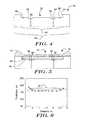
- FIG. 1is a graph representing the profile of a thick photoresist layer applied using a prior art process to different size wafers
- FIG. 2is an elevation view of a wafer holding apparatus in accordance with an illustrative embodiment of the present invention
- FIG. 3is a cross sectional view taken along line 3 — 3 of FIG. 2 ;
- FIG. 4is a cross sectional view of a working embodiment
- FIG. 5is a cross sectional view of the working embodiment from FIG. 4 with a wafer inserted in the pocket and photoresist spun on the surface;
- FIG. 6is a graph representing the profile of a thick photoresist layer applied using a working embodiment of the present invention.
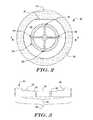
- FIG. 2is an elevation view of a wafer holding apparatus in accordance with an illustrative embodiment of the present invention.
- the wafer holder 30includes a recessed area or pocket 32 .
- the pocket 32includes a channel 34 which is fluidly connected to a number of vacuum holes 36 .
- a raised outer portion 38defines the pocket 32 .
- a waferis placed into the pocket 32 and a vacuum force may be applied using the channel 34 and vacuum holes 36 .
- the use of a channel 34 and vacuum holes 36is merely illustrative of one of many ways a vacuum force may be used to secure a wafer into the pocket 32 .
- the vacuum force/suctionmay include simply using a pressure which is reduced relative to the surrounding atmosphere and need not mean the application of some certain level of vacuum pressure. Additional channels may also be provided in various locations such as, for example, that illustrated in the working embodiment below.
- wafer securing apparatuses or featuresmay be used to replace the channel 34 and vacuum holes 36 .
- clipsmay be provided around the outside of the pocket 32 .
- a wafermay have a hole or holes drilled in, and a screw used to hold the wafer into the pocket 32 .
- Pressuremay be provided from the periphery of the pocket 32 , for example, with a set screw extending through the raised outer portion 38 .
- a tab or tabsmay be provided along the periphery of the pocket 32 such that the wafer may be inserted with the primary or secondary flat aligned to pass by the tabs. The wafer can then be rotated, and pressure may be applied to at least one flat, allowing the tabs to hold the wafer while the flats assure a desired crystalline alignment.
- a receiving primary flat 40is provided to define a part of the border of the pocket 32 .
- An outer primary flat 42is defined on an edge of the wafer holder 30 so the outer primary flat 42 aligns with the receiving primary flat 40 .
- a wafer received in the pocket 32can be treated by processing apparatuses designed for a larger wafer in a way that accounts for the crystalline orientation of the wafer.
- a secondary flatmay be provided as needed for any wafer design.
- a wafer holding apparatus having a secondary flat at an angle of 45 degrees to the primary flatcould be used for an n-type ( 111 ) wafer, an angle of 90 degrees for a p-type ( 100 ) wafer, or an angle of 135 degrees for an n-type ( 100 ) wafer.
- the flatmay be omitted, for example, for additive or surface processes or where specific alignment of the crystalline orientation of the underlying wafer is not needed.
- FIG. 3is a cross sectional view taken along line 3 — 3 of FIG. 2 .
- the pocket 32includes a channel 34 as well as through holes 36 .
- the pocket 32has a height 44 .
- the height 44may be of any desired size. In one illustrative embodiment, the height 44 is chosen to be equal to the thickness of a wafer that is to be held in the pocket 32 . The height 44 may also be chosen to be greater or less than the wafer thickness. In another example, the height 44 is equal to the thickness of a wafer plus some fraction of the desired thickness of a photoresist layer to be deposited on the wafer.
- the pocket 32also has a width 46 which may correspond to the size of a wafer to be received by the pocket 32 .
- the holder 30may have an overall width 48 that is chosen to correspond to a known wafer size, although any appropriate size may be selected.
- the pocket 32has a width 46 corresponding to a 3-inch wafer
- the holder 30has a width 48 corresponding to the size of a 4-inch wafer.
- Other combinationsmay of course be used with 3, 4, 6, 8 or 12 inch wafers, for example, or any other size.
- the holder 30may be made of any material including a variety of metals, plastics, ceramics, glass, or crystalline materials. Some illustrative considerations in choosing the material for the holder may include the compatibility of the material with selected processes to be performed on a wafer held in the holder 30 , cost of the material, or ability to form the material within desired tolerances. Some example compatibility considerations may include durability or strength, density/weight, melting or plastic deformation temperatures, adherence to photoresist, electrically insulative properties, or resistance to etching chemicals. In the working embodiment explained below, the illustrative holder was constructed of aluminum.
- the wafer holder 30is used with devices that apply a suction through channels on a surface.
- many conventional spinning apparatusesinclude channels and/or through holes which apply suction to wafers placed on a rotatable surface.
- the through holes 36may be placed, at least on the bottom of the holder 30 , to correspond to a design of channels and/or holes on the rotatable surface of a spinning apparatus.
- the lower portion of the wafer holder 30may also include channels or other designs that facilitate passage of vacuum force to the through holes 36 .
- the waferwill be held in place in part by the typically sticky photoresist after spinning is completed, and so when the vacuum force is removed the wafer stays in place.
- vacuum pressuremay be applied to hold a wafer in place and the through holes 36 and/or the channel 34 may be plugged to maintain suction.
- the step of plugging the through holes 36may be performed in a vacuum environment by dipping a portion of the back side of the holder into a semi-liquid material, or by placing a cap or other device over the back of the holder.
- a thin plastic adhesive layeri.e. a specially designed tape may also be applied.
- the present inventionmay provide added safety in wafer processing.
- many wafersare quite fragile and the use of a holder may improve durability during processing.
- a person working in a labis often required to wear gloves, making the handling of a wafer difficult.
- the added bulk of the holder 30makes handling easier.
- the wafersthemselves tend to be brittle and the use of a holder may prevent accidental breakage during handling.
- the use of suction applied to the back side of a wafermay also improve surface properties, in particular, reducing curvature caused by differences in the coefficient of thermal expansion of layers of a wafer.
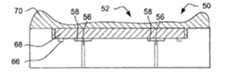
- FIG. 4is a cross sectional view of a working embodiment illustrating various features.
- the working embodiment holder 50was constructed using aluminum.
- the holder 50includes a pocket 52 having a depth 54 of 333 ⁇ m.
- Several through holes 56are in fluid communication with several channels 58 defined in the bottom of the pocket 52 .
- the pocket 52has a width 60 of 3.005 inches (76.33 mm), while the holder 50 has a width 62 of 3.937 inches (100 mm).
- An extra circumferential groove 66is included in the pocket 52 .
- the groove 66serves several purposes as noted below.
- the holder 50was used to illustrate an improved photoresist layer that is spun with a wafer in the holder 50 .
- FIG. 5is a cross sectional view of the working embodiment from FIG. 4 with a wafer inserted in the pocket and photoresist spun on the surface.
- a wafer 68is placed in the pocket 52 , and vacuum suction was applied by the spin apparatus through the through holes 56 .
- There is a gap between the edge of the wafer 68 and the wall of the pocket 52which allows for easier removal of the wafer 68 from the pocket 52 , but which also allows some photoresist 70 to seep around the wafer 68 .
- an amount of photoresistwas placed on the wafer 68 , and the wafer with the holder 50 was spun to spread the photoresist. It should be noted again that the figures are not necessarily to scale.
- a layer of photoresist 70is deposited over the surface of the wafer 68 as well as the wafer holder 50 . It can be seen that the edge bead of the photoresist 70 is actually over the wafer holder 50 , and not the wafer 68 itself. Some of the photoresist 70 seeps beneath the wafer 68 into the groove 66 . The groove 66 helps prevent any of the photoresist 70 from reaching the channel 58 and through hole 56 . After a pre-bake of the photoresist 70 , and before exposure, the edge bead on the photoresist 70 is cleaned off with acetone, allowing for effective use of a contact mask for lithography.
- the wafer holder 50 , wafer 68 and photoresist 70are subjected to development, during which an amount of alcohol or acetone (depending on what is used) seeps into the groove 66 , dissolving and removing the photoresist 70 .
- an amount of alcohol or acetonedepending on what is used
- the alcohol or acetone that seeped into the groove 66boils and evaporates, expanding greatly, and causes the wafer 68 to pop out of the pocket 52 , making the step of removing the wafer 68 from the pocket 52 very simple, easy and clean.
- FIG. 6is a graph representing the profile of a thick photoresist layer applied using a working embodiment of the present invention. Again, the dashed lines illustrate acceptable bounds for the photoresist layer. The acceptable region 80 extends over a greater area of the wafer.
- the result of the working embodimentis that slightly more than 2 inches of the diameter of the three inch wafer is now usable, providing a yield of about 44% of the area of the wafer, nearly double that for the three inch wafer by itself as illustrated in FIG. 1 .
- Use of an even larger wafer holder relative to the wafer 68may yield further improvement.
- a wafer holding apparatusmay be provided which lacks a pocket or recessed area for receiving a wafer.
- the wafer holding apparatusmay include a number of channels and/or through holes which extend to a flat surface on which a wafer may be placed. A suction or vacuum force may then be applied using the through holes to secure the wafer in place on the holder.
Landscapes
- Engineering & Computer Science (AREA)
- Physics & Mathematics (AREA)
- Condensed Matter Physics & Semiconductors (AREA)
- General Physics & Mathematics (AREA)
- Manufacturing & Machinery (AREA)
- Computer Hardware Design (AREA)
- Microelectronics & Electronic Packaging (AREA)
- Power Engineering (AREA)
- Container, Conveyance, Adherence, Positioning, Of Wafer (AREA)
Abstract
Description
Claims (17)
Priority Applications (4)
| Application Number | Priority Date | Filing Date | Title |
|---|---|---|---|
| US10/623,351US6887801B2 (en) | 2003-07-18 | 2003-07-18 | Edge bead control method and apparatus |
| CNA2004800207247ACN1826185A (en) | 2003-07-18 | 2004-07-08 | Edge convex control method and device |
| PCT/US2004/022039WO2005010936A2 (en) | 2003-07-18 | 2004-07-08 | Edge bead control method and apparatus |
| TW093121551ATW200515525A (en) | 2003-07-18 | 2004-07-16 | Edge bead control method and apparatus |
Applications Claiming Priority (1)
| Application Number | Priority Date | Filing Date | Title |
|---|---|---|---|
| US10/623,351US6887801B2 (en) | 2003-07-18 | 2003-07-18 | Edge bead control method and apparatus |
Publications (2)
| Publication Number | Publication Date |
|---|---|
| US20050014390A1 US20050014390A1 (en) | 2005-01-20 |
| US6887801B2true US6887801B2 (en) | 2005-05-03 |
Family
ID=34063363
Family Applications (1)
| Application Number | Title | Priority Date | Filing Date |
|---|---|---|---|
| US10/623,351Expired - Fee RelatedUS6887801B2 (en) | 2003-07-18 | 2003-07-18 | Edge bead control method and apparatus |
Country Status (4)
| Country | Link |
|---|---|
| US (1) | US6887801B2 (en) |
| CN (1) | CN1826185A (en) |
| TW (1) | TW200515525A (en) |
| WO (1) | WO2005010936A2 (en) |
Families Citing this family (5)
| Publication number | Priority date | Publication date | Assignee | Title |
|---|---|---|---|---|
| KR100518788B1 (en)* | 2003-03-11 | 2005-10-05 | 삼성전자주식회사 | Spin coating apparatus for coating photoresist |
| US8619072B2 (en)* | 2009-03-04 | 2013-12-31 | Triangle Software Llc | Controlling a three-dimensional virtual broadcast presentation |
| CN102862396A (en)* | 2012-08-04 | 2013-01-09 | 江苏吉星新材料有限公司 | Chip marking positioning die |
| US10978332B2 (en)* | 2016-10-05 | 2021-04-13 | Prilit Optronics, Inc. | Vacuum suction apparatus |
| CN117497435A (en)* | 2022-07-21 | 2024-02-02 | 长鑫存储技术有限公司 | Semiconductor structure processing method, processing device and processing system |
Citations (148)
| Publication number | Priority date | Publication date | Assignee | Title |
|---|---|---|---|---|
| US4317085A (en) | 1979-09-12 | 1982-02-23 | Xerox Corporation | Channeled mesa laser |
| US4466694A (en) | 1978-06-15 | 1984-08-21 | Her Majesty The Queen In Right Of Canada, As Represented By The Minister Of National Defence Of Her Majesty's Canadian Government | Wavelength selective optical coupler |
| JPS60123084A (en) | 1983-12-08 | 1985-07-01 | Matsushita Electric Ind Co Ltd | semiconductor light generator |
| US4660207A (en) | 1984-11-21 | 1987-04-21 | Northern Telecom Limited | Surface-emitting light emitting device |
| US4675058A (en) | 1983-12-14 | 1987-06-23 | Honeywell Inc. | Method of manufacturing a high-bandwidth, high radiance, surface emitting LED |
| EP0288184A2 (en) | 1987-04-21 | 1988-10-26 | Gec-Marconi Limited | Semiconductor diode laser array |
| US4784722A (en) | 1985-01-22 | 1988-11-15 | Massachusetts Institute Of Technology | Method forming surface emitting diode laser |
| US4885592A (en) | 1987-12-28 | 1989-12-05 | Kofol J Stephen | Electronically steerable antenna |
| US4901327A (en) | 1988-10-24 | 1990-02-13 | General Dynamics Corporation, Electronics Division | Transverse injection surface emitting laser |
| US4943970A (en) | 1988-10-24 | 1990-07-24 | General Dynamics Corporation, Electronics Division | Surface emitting laser |
| US4956844A (en) | 1989-03-17 | 1990-09-11 | Massachusetts Institute Of Technology | Two-dimensional surface-emitting laser array |
| JPH0254981B2 (en) | 1984-06-25 | 1990-11-26 | Fujitsu Ltd | |
| US5031187A (en) | 1990-02-14 | 1991-07-09 | Bell Communications Research, Inc. | Planar array of vertical-cavity, surface-emitting lasers |
| US5052016A (en) | 1990-05-18 | 1991-09-24 | University Of New Mexico | Resonant-periodic-gain distributed-feedback surface-emitting semiconductor laser |
| US5056098A (en) | 1990-07-05 | 1991-10-08 | At&T Bell Laboratories | Vertical cavity laser with mirror having controllable reflectivity |
| US5062115A (en) | 1990-12-28 | 1991-10-29 | Xerox Corporation | High density, independently addressable, surface emitting semiconductor laser/light emitting diode arrays |
| US5068869A (en) | 1987-06-19 | 1991-11-26 | Lockheed Missiles & Space Company, Inc. | Surface-emitting laser diode |
| US5079774A (en) | 1990-12-27 | 1992-01-07 | International Business Machines Corporation | Polarization-tunable optoelectronic devices |
| US5115442A (en) | 1990-04-13 | 1992-05-19 | At&T Bell Laboratories | Top-emitting surface emitting laser structures |
| US5117469A (en) | 1991-02-01 | 1992-05-26 | Bell Communications Research, Inc. | Polarization-dependent and polarization-diversified opto-electronic devices using a strained quantum well |
| US5140605A (en) | 1991-06-27 | 1992-08-18 | Xerox Corporation | Thermally stabilized diode laser structure |
| US5157537A (en) | 1991-02-01 | 1992-10-20 | Yeda Research And Development Co., Ltd. | Distributed resonant cavity light beam modulator |
| US5158908A (en) | 1990-08-31 | 1992-10-27 | At&T Bell Laboratories | Distributed bragg reflectors and devices incorporating same |
| US5212706A (en) | 1991-12-03 | 1993-05-18 | University Of Connecticut | Laser diode assembly with tunnel junctions and providing multiple beams |
| US5216263A (en) | 1990-11-29 | 1993-06-01 | Xerox Corporation | High density, independently addressable, surface emitting semiconductor laser-light emitting diode arrays |
| US5216680A (en) | 1991-07-11 | 1993-06-01 | Board Of Regents, The University Of Texas System | Optical guided-mode resonance filter |
| US5237581A (en) | 1990-11-14 | 1993-08-17 | Nec Corporation | Semiconductor multilayer reflector and light emitting device with the same |
| US5245622A (en) | 1992-05-07 | 1993-09-14 | Bandgap Technology Corporation | Vertical-cavity surface-emitting lasers with intra-cavity structures |
| US5258990A (en) | 1991-11-07 | 1993-11-02 | The United States Of America As Represented By The Secretary Of The United States Department Of Energy | Visible light surface emitting semiconductor laser |
| US5262360A (en) | 1990-12-31 | 1993-11-16 | The Board Of Trustees Of The University Of Illinois | AlGaAs native oxide |
| US5285466A (en) | 1992-05-20 | 1994-02-08 | Wisconsin Alumni Research Foundation | Feedback mechanism for vertical cavity surface emitting lasers |
| US5293392A (en) | 1992-07-31 | 1994-03-08 | Motorola, Inc. | Top emitting VCSEL with etch stop layer |
| US5317587A (en) | 1992-08-06 | 1994-05-31 | Motorola, Inc. | VCSEL with separate control of current distribution and optical mode |
| DE4240706A1 (en) | 1992-12-03 | 1994-06-09 | Siemens Ag | Surface emitting laser diode |
| US5325386A (en) | 1992-04-21 | 1994-06-28 | Bandgap Technology Corporation | Vertical-cavity surface emitting laser assay display system |
| US5331654A (en) | 1993-03-05 | 1994-07-19 | Photonics Research Incorporated | Polarized surface-emitting laser |
| US5337183A (en) | 1991-02-01 | 1994-08-09 | Yeda Research And Development Co. Ltd. | Distributed resonant cavity light beam modulator |
| US5349599A (en) | 1990-03-29 | 1994-09-20 | Larkins Eric C | Bistable optical laser based on a heterostructure PNPN thyristor |
| US5351256A (en) | 1993-04-28 | 1994-09-27 | The United States Of America As Represented By The United States Department Of Energy | Electrically injected visible vertical cavity surface emitting laser diodes |
| US5359447A (en) | 1993-06-25 | 1994-10-25 | Hewlett-Packard Company | Optical communication with vertical-cavity surface-emitting laser operating in multiple transverse modes |
| US5359618A (en) | 1993-06-01 | 1994-10-25 | Motorola, Inc. | High efficiency VCSEL and method of fabrication |
| US5363397A (en) | 1992-10-29 | 1994-11-08 | Internatioal Business Machines Corporation | Integrated short cavity laser with bragg mirrors |
| US5373520A (en) | 1992-08-12 | 1994-12-13 | Fujitsu Limited | Surface emitting laser and method of manufacturing the same |
| US5376580A (en) | 1993-03-19 | 1994-12-27 | Hewlett-Packard Company | Wafer bonding of light emitting diode layers |
| US5386426A (en) | 1992-09-10 | 1995-01-31 | Hughes Aircraft Company | Narrow bandwidth laser array system |
| US5390209A (en) | 1994-01-05 | 1995-02-14 | At&T Corp. | Article comprising a semiconductor laser that is non-degenerate with regard to polarization |
| US5396508A (en) | 1992-09-22 | 1995-03-07 | Xerox Corporation | Polarization switchable quantum well laser |
| US5404373A (en) | 1991-11-08 | 1995-04-04 | University Of New Mexico | Electro-optical device |
| US5412680A (en) | 1994-03-18 | 1995-05-02 | Photonics Research Incorporated | Linear polarization of semiconductor laser |
| US5412678A (en) | 1992-09-22 | 1995-05-02 | Xerox Corporation | Multi-beam, orthogonally-polarized emitting monolithic quantum well lasers |
| US5416044A (en) | 1993-03-12 | 1995-05-16 | Matsushita Electric Industrial Co., Ltd. | Method for producing a surface-emitting laser |
| US5428634A (en) | 1992-11-05 | 1995-06-27 | The United States Of America As Represented By The United States Department Of Energy | Visible light emitting vertical cavity surface emitting lasers |
| US5438584A (en) | 1992-09-22 | 1995-08-01 | Xerox Corporation | Dual polarization laser diode with quaternary material system |
| US5446754A (en) | 1993-11-05 | 1995-08-29 | Photonics Research Incorporated | Phased array semiconductor laser |
| US5465263A (en) | 1992-12-12 | 1995-11-07 | Xerox Corporation | Monolithic, multiple wavelength, dual polarization laser diode arrays |
| US5475701A (en) | 1993-12-29 | 1995-12-12 | Honeywell Inc. | Integrated laser power monitor |
| US5493577A (en) | 1994-12-21 | 1996-02-20 | Sandia Corporation | Efficient semiconductor light-emitting device and method |
| US5497390A (en) | 1992-01-31 | 1996-03-05 | Nippon Telegraph And Telephone Corporation | Polarization mode switching semiconductor laser apparatus |
| US5513202A (en) | 1994-02-25 | 1996-04-30 | Matsushita Electric Industrial Co., Ltd. | Vertical-cavity surface-emitting semiconductor laser |
| US5530715A (en) | 1994-11-29 | 1996-06-25 | Motorola, Inc. | Vertical cavity surface emitting laser having continuous grading |
| US5557626A (en) | 1994-06-15 | 1996-09-17 | Motorola | Patterned mirror VCSEL with adjustable selective etch region |
| US5561683A (en) | 1994-01-27 | 1996-10-01 | Kwon; O'dae | Circular grating surface emitting laser diode |
| US5568499A (en) | 1995-04-07 | 1996-10-22 | Sandia Corporation | Optical device with low electrical and thermal resistance bragg reflectors |
| US5568498A (en) | 1993-09-10 | 1996-10-22 | Telefonaktiebolaget Lm Ericsson | Laser device with laser structures connected in series in an optical cavity |
| US5574738A (en) | 1995-06-07 | 1996-11-12 | Honeywell Inc. | Multi-gigahertz frequency-modulated vertical-cavity surface emitting laser |
| US5581571A (en) | 1994-04-08 | 1996-12-03 | The Board Of Trustees Of The University Of Illinois | Semiconductor devices and methods |
| US5586131A (en) | 1993-12-10 | 1996-12-17 | Canon Kabushiki Kaisha | Oscillation polarization mode selective semiconductor laser, light source apparatus and optical communication system using the laser |
| US5590145A (en) | 1994-02-23 | 1996-12-31 | Canon Kabushiki Kaisha | Light-emitting apparatus capable of selecting polarization direction, optical communication system, and polarization modulation control method |
| US5598300A (en) | 1995-06-05 | 1997-01-28 | Board Of Regents, The University Of Texas System | Efficient bandpass reflection and transmission filters with low sidebands based on guided-mode resonance effects |
| US5606572A (en) | 1994-03-24 | 1997-02-25 | Vixel Corporation | Integration of laser with photodiode for feedback control |
| US5625729A (en) | 1994-08-12 | 1997-04-29 | Brown; Thomas G. | Optoelectronic device for coupling between an external optical wave and a local optical wave for optical modulators and detectors |
| EP0776076A1 (en) | 1995-11-21 | 1997-05-28 | Thomson-Csf | Optoelectronic quantum well device |
| US5645462A (en) | 1991-10-08 | 1997-07-08 | Canon Kabushiki Kaisha | Electron-emitting device, and electron beam-generating apparatus and image-forming apparatus employing the device |
| US5646978A (en) | 1995-04-27 | 1997-07-08 | Lucent Technologies Inc. | Method and apparatus for providing interswitch handover in personal communication services systems |
| US5648978A (en) | 1995-01-04 | 1997-07-15 | Canon Kabushiki Kaisha | Oscillation polarization mode selective semiconductor laser, modulation method therefor and optical communication system using the same |
| US5679963A (en) | 1995-12-05 | 1997-10-21 | Sandia Corporation | Semiconductor tunnel junction with enhancement layer |
| US5692083A (en) | 1996-03-13 | 1997-11-25 | The Whitaker Corporation | In-line unitary optical device mount and package therefor |
| US5699373A (en) | 1994-03-17 | 1997-12-16 | Canon Kabushiki Kaisha | Oscillation polarization selective semiconductor laser and optical communication system using the same |
| US5712188A (en) | 1995-12-21 | 1998-01-27 | Electronics And Telecommunications Research Institute | Fabrication method of polarization-controlled surface-emitting laser diode using tilted-cavity |
| US5727013A (en) | 1995-10-27 | 1998-03-10 | Wisconsin Alumni Research Foundation | Single lobe surface emitting complex coupled distributed feedback semiconductor laser |
| US5726805A (en) | 1996-06-25 | 1998-03-10 | Sandia Corporation | Optical filter including a sub-wavelength periodic structure and method of making |
| US5727014A (en) | 1995-10-31 | 1998-03-10 | Hewlett-Packard Company | Vertical-cavity surface-emitting laser generating light with a defined direction of polarization |
| US5774487A (en) | 1996-10-16 | 1998-06-30 | Honeywell Inc. | Filamented multi-wavelength vertical-cavity surface emitting laser |
| US5778018A (en) | 1994-10-13 | 1998-07-07 | Nec Corporation | VCSELs (vertical-cavity surface emitting lasers) and VCSEL-based devices |
| US5781575A (en) | 1993-09-10 | 1998-07-14 | Telefonaktiebolaget Lm Ericsson | Surface emitting laser device with a vertical cavity |
| US5784399A (en) | 1996-12-19 | 1998-07-21 | Xerox Corporation | Polarization mode selection by distributed Bragg reflector in a quantum well laser |
| US5790733A (en) | 1996-06-07 | 1998-08-04 | Minnesota Mining And Manufactouring Company | Optoelectronic device receptacle and method of making same |
| US5805624A (en) | 1996-07-30 | 1998-09-08 | Hewlett-Packard Company | Long-wavelength infra-red vertical cavity surface-emitting laser on a gallium arsenide substrate |
| US5828684A (en) | 1995-12-29 | 1998-10-27 | Xerox Corporation | Dual polarization quantum well laser in the 200 to 600 nanometers range |
| US5838705A (en) | 1996-11-04 | 1998-11-17 | Motorola, Inc. | Light emitting device having a defect inhibition layer |
| US5838715A (en) | 1996-06-20 | 1998-11-17 | Hewlett-Packard Company | High intensity single-mode VCSELs |
| WO1998057402A1 (en) | 1997-06-11 | 1998-12-17 | Honeywell Inc. | Resonant reflector for improved optoelectronic device performance and enhanced applicability |
| US5892784A (en) | 1994-10-27 | 1999-04-06 | Hewlett-Packard Company | N-drive p-common surface emitting laser fabricated on n+ substrate |
| US5892787A (en) | 1994-10-27 | 1999-04-06 | Hewlett-Packard Company | N-drive, p-common light-emitting devices fabricated on an n-type substrate and method of making same |
| US5896408A (en) | 1997-08-15 | 1999-04-20 | Hewlett-Packard Company | Near planar native-oxide VCSEL devices and arrays using converging oxide ringlets |
| US5901166A (en) | 1994-02-18 | 1999-05-04 | Canon Kabushiki Kaisha | Oscillation polarization mode selective semiconductor laser, light transmitter and optical communication system using the laser |
| US5903590A (en) | 1996-05-20 | 1999-05-11 | Sandia Corporation | Vertical-cavity surface-emitting laser device |
| US5903589A (en) | 1995-12-18 | 1999-05-11 | Picolight, Incorporated | Oxidizable semiconductor device having cavities which allow for improved oxidation of the semiconductor device |
| US5903588A (en) | 1997-03-06 | 1999-05-11 | Honeywell Inc. | Laser with a selectively changed current confining layer |
| US5908408A (en) | 1996-09-13 | 1999-06-01 | Mcgary; R. Kern | Non-reusable retractable safety syringe |
| US5908661A (en)* | 1997-05-30 | 1999-06-01 | The Fairchild Corporation | Apparatus and method for spin coating substrates |
| US5936266A (en) | 1997-07-22 | 1999-08-10 | The Board Of Trustees Of The University Of Illinois | Semiconductor devices and methods with tunnel contact hole sources |
| US5940422A (en) | 1996-06-28 | 1999-08-17 | Honeywell Inc. | Laser with an improved mode control |
| US5953362A (en) | 1997-12-15 | 1999-09-14 | Pamulapati; Jagadeesh | Strain induce control of polarization states in vertical cavity surface emitting lasers and method of making same |
| US5978408A (en) | 1997-02-07 | 1999-11-02 | Xerox Corporation | Highly compact vertical cavity surface emitting lasers |
| US5978401A (en) | 1995-10-25 | 1999-11-02 | Honeywell Inc. | Monolithic vertical cavity surface emitting laser and resonant cavity photodetector transceiver |
| US5995531A (en) | 1997-11-04 | 1999-11-30 | Motorola, Inc. | VCSEL having polarization control and method of making same |
| US6002705A (en) | 1997-12-03 | 1999-12-14 | Xerox Corporation | Wavelength and polarization multiplexed vertical cavity surface emitting lasers |
| US6008675A (en) | 1996-07-31 | 1999-12-28 | Canon Kabushiki Kaisha | Polarization-mode selective semiconductor laser with a bending channel stripe, apparatus including the same and optical communication system using the same |
| US6043104A (en) | 1996-08-28 | 2000-03-28 | Canon Kabushiki Kaisha | Fabrication method of a polarization selective semiconductor laser |
| US6046065A (en) | 1996-09-13 | 2000-04-04 | Alcatel | Process for fabricating a semiconductor opto-electronic component and component and matrix of components fabricated by this process |
| US6052398A (en) | 1997-04-03 | 2000-04-18 | Alcatel | Surface emitting semiconductor laser |
| US6060743A (en) | 1997-05-21 | 2000-05-09 | Kabushiki Kaisha Toshiba | Semiconductor memory device having multilayer group IV nanocrystal quantum dot floating gate and method of manufacturing the same |
| US6078601A (en) | 1997-03-07 | 2000-06-20 | Smith; David F. | Method for controlling the operation of a laser |
| US6086263A (en) | 1996-06-13 | 2000-07-11 | 3M Innovative Properties Company | Active device receptacle |
| US6133590A (en) | 1995-11-29 | 2000-10-17 | The Secretary Of State For Defence In Her Britannic Majesty's Government Of The United Kingdom Of Great Britain And Northern Irelands | Low resistance contact semiconductor diode |
| US6144682A (en) | 1998-10-29 | 2000-11-07 | Xerox Corporation | Spatial absorptive and phase shift filter layer to reduce modal reflectivity for higher order modes in a vertical cavity surface emitting laser |
| US6154480A (en) | 1997-10-02 | 2000-11-28 | Board Of Regents, The University Of Texas System | Vertical-cavity laser and laser array incorporating guided-mode resonance effects and method for making the same |
| US6185241B1 (en) | 1998-10-29 | 2001-02-06 | Xerox Corporation | Metal spatial filter to enhance model reflectivity in a vertical cavity surface emitting laser |
| US6191890B1 (en) | 1996-03-29 | 2001-02-20 | Interuniversitair Micro-Elektronica Centrum Vzw | Optical system with a dielectric subwavelength structure having high reflectivity and polarization selectivity |
| US6212312B1 (en) | 1999-09-17 | 2001-04-03 | U.T. Battelle, Llc | Optical multiplexer/demultiplexer using resonant grating filters |
| US6238944B1 (en) | 1999-12-21 | 2001-05-29 | Xerox Corporation | Buried heterostructure vertical-cavity surface-emitting laser diodes using impurity induced layer disordering (IILD) via a buried impurity source |
| US20010004414A1 (en) | 1999-12-13 | 2001-06-21 | Gerhard Kuhn | Coupling configuration |
| US6302596B1 (en) | 1999-07-07 | 2001-10-16 | International Business Machines Corporation | Small form factor optoelectronic transceivers |
| US6339496B1 (en) | 1999-06-22 | 2002-01-15 | University Of Maryland | Cavity-less vertical semiconductor optical amplifier |
| US6369403B1 (en) | 1999-05-27 | 2002-04-09 | The Board Of Trustees Of The University Of Illinois | Semiconductor devices and methods with tunnel contact hole sources and non-continuous barrier layer |
| US6372533B2 (en) | 1998-11-05 | 2002-04-16 | Gore Enterprise Holdings, Inc. | Method of making a semiconductor device with aligned oxide apertures and contact to an intervening layer |
| US6392257B1 (en) | 2000-02-10 | 2002-05-21 | Motorola Inc. | Semiconductor structure, semiconductor device, communicating device, integrated circuit, and process for fabricating the same |
| US6411638B1 (en) | 1999-08-31 | 2002-06-25 | Honeywell Inc. | Coupled cavity anti-guided vertical-cavity surface-emitting laser |
| US6410941B1 (en) | 2000-06-30 | 2002-06-25 | Motorola, Inc. | Reconfigurable systems using hybrid integrated circuits with optical ports |
| US6427066B1 (en) | 2000-06-30 | 2002-07-30 | Motorola, Inc. | Apparatus and method for effecting communications among a plurality of remote stations |
| US6459709B1 (en) | 2001-01-31 | 2002-10-01 | Nova Crystals, Inc. | Wavelength-tunable semiconductor laser diode |
| US6462360B1 (en) | 2001-08-06 | 2002-10-08 | Motorola, Inc. | Integrated gallium arsenide communications systems |
| US6472694B1 (en) | 2001-07-23 | 2002-10-29 | Motorola, Inc. | Microprocessor structure having a compound semiconductor layer |
| US6477285B1 (en) | 2000-06-30 | 2002-11-05 | Motorola, Inc. | Integrated circuits with optical signal propagation |
| US6487230B1 (en) | 1998-04-14 | 2002-11-26 | Bandwidth 9, Inc | Vertical cavity apparatus with tunnel junction |
| US6487231B1 (en) | 1998-04-14 | 2002-11-26 | Bandwidth 9, Inc. | Vertical cavity apparatus with tunnel junction |
| US6490311B1 (en) | 1998-04-14 | 2002-12-03 | Bandwidth 9, Inc. | Vertical cavity apparatus with tunnel junction |
| US6493373B1 (en) | 1998-04-14 | 2002-12-10 | Bandwidth 9, Inc. | Vertical cavity apparatus with tunnel junction |
| US6493371B1 (en) | 1998-04-14 | 2002-12-10 | Bandwidth9, Inc. | Vertical cavity apparatus with tunnel junction |
| US6493372B1 (en) | 1998-04-14 | 2002-12-10 | Bandwidth 9, Inc. | Vertical cavity apparatus with tunnel junction |
| US6496621B1 (en) | 1998-09-22 | 2002-12-17 | Digital Optics Corp. | Fiber coupler system and associated methods for reducing back reflections |
| US6498358B1 (en) | 2001-07-20 | 2002-12-24 | Motorola, Inc. | Structure and method for fabricating an electro-optic system having an electrochromic diffraction grating |
| US6501973B1 (en) | 2000-06-30 | 2002-12-31 | Motorola, Inc. | Apparatus and method for measuring selected physical condition of an animate subject |
| US6515308B1 (en) | 2001-12-21 | 2003-02-04 | Xerox Corporation | Nitride-based VCSEL or light emitting diode with p-n tunnel junction current injection |
| US6535541B1 (en) | 1998-04-14 | 2003-03-18 | Bandwidth 9, Inc | Vertical cavity apparatus with tunnel junction |
| US6542531B2 (en) | 2001-03-15 | 2003-04-01 | Ecole Polytechnique Federale De Lausanne | Vertical cavity surface emitting laser and a method of fabrication thereof |
| US6567435B1 (en) | 1999-03-19 | 2003-05-20 | Optical Communication Products, Inc. | VCSEL power monitoring system using plastic encapsulation techniques |
- 2003
- 2003-07-18USUS10/623,351patent/US6887801B2/ennot_activeExpired - Fee Related
- 2004
- 2004-07-08WOPCT/US2004/022039patent/WO2005010936A2/enactiveApplication Filing
- 2004-07-08CNCNA2004800207247Apatent/CN1826185A/enactivePending
- 2004-07-16TWTW093121551Apatent/TW200515525A/enunknown
Patent Citations (164)
| Publication number | Priority date | Publication date | Assignee | Title |
|---|---|---|---|---|
| US4466694A (en) | 1978-06-15 | 1984-08-21 | Her Majesty The Queen In Right Of Canada, As Represented By The Minister Of National Defence Of Her Majesty's Canadian Government | Wavelength selective optical coupler |
| US4317085A (en) | 1979-09-12 | 1982-02-23 | Xerox Corporation | Channeled mesa laser |
| JPS60123084A (en) | 1983-12-08 | 1985-07-01 | Matsushita Electric Ind Co Ltd | semiconductor light generator |
| US4675058A (en) | 1983-12-14 | 1987-06-23 | Honeywell Inc. | Method of manufacturing a high-bandwidth, high radiance, surface emitting LED |
| JPH0254981B2 (en) | 1984-06-25 | 1990-11-26 | Fujitsu Ltd | |
| US4660207A (en) | 1984-11-21 | 1987-04-21 | Northern Telecom Limited | Surface-emitting light emitting device |
| US4784722A (en) | 1985-01-22 | 1988-11-15 | Massachusetts Institute Of Technology | Method forming surface emitting diode laser |
| EP0288184A2 (en) | 1987-04-21 | 1988-10-26 | Gec-Marconi Limited | Semiconductor diode laser array |
| US5068869A (en) | 1987-06-19 | 1991-11-26 | Lockheed Missiles & Space Company, Inc. | Surface-emitting laser diode |
| US4885592A (en) | 1987-12-28 | 1989-12-05 | Kofol J Stephen | Electronically steerable antenna |
| US4901327A (en) | 1988-10-24 | 1990-02-13 | General Dynamics Corporation, Electronics Division | Transverse injection surface emitting laser |
| US4943970A (en) | 1988-10-24 | 1990-07-24 | General Dynamics Corporation, Electronics Division | Surface emitting laser |
| US4956844A (en) | 1989-03-17 | 1990-09-11 | Massachusetts Institute Of Technology | Two-dimensional surface-emitting laser array |
| US5031187A (en) | 1990-02-14 | 1991-07-09 | Bell Communications Research, Inc. | Planar array of vertical-cavity, surface-emitting lasers |
| US5349599A (en) | 1990-03-29 | 1994-09-20 | Larkins Eric C | Bistable optical laser based on a heterostructure PNPN thyristor |
| US5115442A (en) | 1990-04-13 | 1992-05-19 | At&T Bell Laboratories | Top-emitting surface emitting laser structures |
| US5052016A (en) | 1990-05-18 | 1991-09-24 | University Of New Mexico | Resonant-periodic-gain distributed-feedback surface-emitting semiconductor laser |
| US5056098A (en) | 1990-07-05 | 1991-10-08 | At&T Bell Laboratories | Vertical cavity laser with mirror having controllable reflectivity |
| US5158908A (en) | 1990-08-31 | 1992-10-27 | At&T Bell Laboratories | Distributed bragg reflectors and devices incorporating same |
| US5237581A (en) | 1990-11-14 | 1993-08-17 | Nec Corporation | Semiconductor multilayer reflector and light emitting device with the same |
| US5317170A (en) | 1990-11-29 | 1994-05-31 | Xerox Corporation | High density, independently addressable, surface emitting semiconductor laser/light emitting diode arrays without a substrate |
| US5216263A (en) | 1990-11-29 | 1993-06-01 | Xerox Corporation | High density, independently addressable, surface emitting semiconductor laser-light emitting diode arrays |
| US5079774A (en) | 1990-12-27 | 1992-01-07 | International Business Machines Corporation | Polarization-tunable optoelectronic devices |
| US5062115A (en) | 1990-12-28 | 1991-10-29 | Xerox Corporation | High density, independently addressable, surface emitting semiconductor laser/light emitting diode arrays |
| US5337074A (en) | 1990-12-28 | 1994-08-09 | Xerox Corporation | Opto-electronic line printer having a high density, independently addressable, surface emitting semiconductor laser/light emitting diode array |
| US5262360A (en) | 1990-12-31 | 1993-11-16 | The Board Of Trustees Of The University Of Illinois | AlGaAs native oxide |
| US5373522A (en) | 1990-12-31 | 1994-12-13 | The Board Of Trustees Of The University Of Illinois | Semiconductor devices with native aluminum oxide regions |
| US5567980A (en) | 1990-12-31 | 1996-10-22 | The Board Of Trustees Of The University Of Illinois | Native oxide of an aluminum-bearing group III-V semiconductor |
| US5696023A (en) | 1990-12-31 | 1997-12-09 | The Board Of Trustees Of The University Of Illinois | Method for making aluminum gallium arsenide semiconductor device with native oxide layer |
| US5117469A (en) | 1991-02-01 | 1992-05-26 | Bell Communications Research, Inc. | Polarization-dependent and polarization-diversified opto-electronic devices using a strained quantum well |
| US5337183A (en) | 1991-02-01 | 1994-08-09 | Yeda Research And Development Co. Ltd. | Distributed resonant cavity light beam modulator |
| US5157537A (en) | 1991-02-01 | 1992-10-20 | Yeda Research And Development Co., Ltd. | Distributed resonant cavity light beam modulator |
| US5140605A (en) | 1991-06-27 | 1992-08-18 | Xerox Corporation | Thermally stabilized diode laser structure |
| US5216680A (en) | 1991-07-11 | 1993-06-01 | Board Of Regents, The University Of Texas System | Optical guided-mode resonance filter |
| US5645462A (en) | 1991-10-08 | 1997-07-08 | Canon Kabushiki Kaisha | Electron-emitting device, and electron beam-generating apparatus and image-forming apparatus employing the device |
| US5258990A (en) | 1991-11-07 | 1993-11-02 | The United States Of America As Represented By The Secretary Of The United States Department Of Energy | Visible light surface emitting semiconductor laser |
| US5642376A (en) | 1991-11-07 | 1997-06-24 | Vixel Corporation | Visible light surface emitting semiconductor laser |
| US5404373A (en) | 1991-11-08 | 1995-04-04 | University Of New Mexico | Electro-optical device |
| US5212706A (en) | 1991-12-03 | 1993-05-18 | University Of Connecticut | Laser diode assembly with tunnel junctions and providing multiple beams |
| US5497390A (en) | 1992-01-31 | 1996-03-05 | Nippon Telegraph And Telephone Corporation | Polarization mode switching semiconductor laser apparatus |
| US5325386A (en) | 1992-04-21 | 1994-06-28 | Bandgap Technology Corporation | Vertical-cavity surface emitting laser assay display system |
| US5245622A (en) | 1992-05-07 | 1993-09-14 | Bandgap Technology Corporation | Vertical-cavity surface-emitting lasers with intra-cavity structures |
| US5285466A (en) | 1992-05-20 | 1994-02-08 | Wisconsin Alumni Research Foundation | Feedback mechanism for vertical cavity surface emitting lasers |
| US5293392A (en) | 1992-07-31 | 1994-03-08 | Motorola, Inc. | Top emitting VCSEL with etch stop layer |
| US5317587A (en) | 1992-08-06 | 1994-05-31 | Motorola, Inc. | VCSEL with separate control of current distribution and optical mode |
| US5373520A (en) | 1992-08-12 | 1994-12-13 | Fujitsu Limited | Surface emitting laser and method of manufacturing the same |
| US5386426A (en) | 1992-09-10 | 1995-01-31 | Hughes Aircraft Company | Narrow bandwidth laser array system |
| US5412678A (en) | 1992-09-22 | 1995-05-02 | Xerox Corporation | Multi-beam, orthogonally-polarized emitting monolithic quantum well lasers |
| US5396508A (en) | 1992-09-22 | 1995-03-07 | Xerox Corporation | Polarization switchable quantum well laser |
| US5438584A (en) | 1992-09-22 | 1995-08-01 | Xerox Corporation | Dual polarization laser diode with quaternary material system |
| US5363397A (en) | 1992-10-29 | 1994-11-08 | Internatioal Business Machines Corporation | Integrated short cavity laser with bragg mirrors |
| US5428634A (en) | 1992-11-05 | 1995-06-27 | The United States Of America As Represented By The United States Department Of Energy | Visible light emitting vertical cavity surface emitting lasers |
| US5555255A (en) | 1992-12-03 | 1996-09-10 | Siemens Aktiengesellschaft | Surface-emitting laser diode |
| DE4240706A1 (en) | 1992-12-03 | 1994-06-09 | Siemens Ag | Surface emitting laser diode |
| US5465263A (en) | 1992-12-12 | 1995-11-07 | Xerox Corporation | Monolithic, multiple wavelength, dual polarization laser diode arrays |
| US5331654A (en) | 1993-03-05 | 1994-07-19 | Photonics Research Incorporated | Polarized surface-emitting laser |
| US5416044A (en) | 1993-03-12 | 1995-05-16 | Matsushita Electric Industrial Co., Ltd. | Method for producing a surface-emitting laser |
| US5376580A (en) | 1993-03-19 | 1994-12-27 | Hewlett-Packard Company | Wafer bonding of light emitting diode layers |
| US5351256A (en) | 1993-04-28 | 1994-09-27 | The United States Of America As Represented By The United States Department Of Energy | Electrically injected visible vertical cavity surface emitting laser diodes |
| US5359618A (en) | 1993-06-01 | 1994-10-25 | Motorola, Inc. | High efficiency VCSEL and method of fabrication |
| US5359447A (en) | 1993-06-25 | 1994-10-25 | Hewlett-Packard Company | Optical communication with vertical-cavity surface-emitting laser operating in multiple transverse modes |
| US5568498A (en) | 1993-09-10 | 1996-10-22 | Telefonaktiebolaget Lm Ericsson | Laser device with laser structures connected in series in an optical cavity |
| US5781575A (en) | 1993-09-10 | 1998-07-14 | Telefonaktiebolaget Lm Ericsson | Surface emitting laser device with a vertical cavity |
| US5446754A (en) | 1993-11-05 | 1995-08-29 | Photonics Research Incorporated | Phased array semiconductor laser |
| US5586131A (en) | 1993-12-10 | 1996-12-17 | Canon Kabushiki Kaisha | Oscillation polarization mode selective semiconductor laser, light source apparatus and optical communication system using the laser |
| US5475701A (en) | 1993-12-29 | 1995-12-12 | Honeywell Inc. | Integrated laser power monitor |
| US5390209A (en) | 1994-01-05 | 1995-02-14 | At&T Corp. | Article comprising a semiconductor laser that is non-degenerate with regard to polarization |
| US5561683A (en) | 1994-01-27 | 1996-10-01 | Kwon; O'dae | Circular grating surface emitting laser diode |
| US5901166A (en) | 1994-02-18 | 1999-05-04 | Canon Kabushiki Kaisha | Oscillation polarization mode selective semiconductor laser, light transmitter and optical communication system using the laser |
| US5590145A (en) | 1994-02-23 | 1996-12-31 | Canon Kabushiki Kaisha | Light-emitting apparatus capable of selecting polarization direction, optical communication system, and polarization modulation control method |
| US5513202A (en) | 1994-02-25 | 1996-04-30 | Matsushita Electric Industrial Co., Ltd. | Vertical-cavity surface-emitting semiconductor laser |
| US5699373A (en) | 1994-03-17 | 1997-12-16 | Canon Kabushiki Kaisha | Oscillation polarization selective semiconductor laser and optical communication system using the same |
| US5412680A (en) | 1994-03-18 | 1995-05-02 | Photonics Research Incorporated | Linear polarization of semiconductor laser |
| US5606572A (en) | 1994-03-24 | 1997-02-25 | Vixel Corporation | Integration of laser with photodiode for feedback control |
| US5581571A (en) | 1994-04-08 | 1996-12-03 | The Board Of Trustees Of The University Of Illinois | Semiconductor devices and methods |
| US5557626A (en) | 1994-06-15 | 1996-09-17 | Motorola | Patterned mirror VCSEL with adjustable selective etch region |
| US5625729A (en) | 1994-08-12 | 1997-04-29 | Brown; Thomas G. | Optoelectronic device for coupling between an external optical wave and a local optical wave for optical modulators and detectors |
| US5778018A (en) | 1994-10-13 | 1998-07-07 | Nec Corporation | VCSELs (vertical-cavity surface emitting lasers) and VCSEL-based devices |
| US5892787A (en) | 1994-10-27 | 1999-04-06 | Hewlett-Packard Company | N-drive, p-common light-emitting devices fabricated on an n-type substrate and method of making same |
| US5892784A (en) | 1994-10-27 | 1999-04-06 | Hewlett-Packard Company | N-drive p-common surface emitting laser fabricated on n+ substrate |
| US5530715A (en) | 1994-11-29 | 1996-06-25 | Motorola, Inc. | Vertical cavity surface emitting laser having continuous grading |
| US5493577A (en) | 1994-12-21 | 1996-02-20 | Sandia Corporation | Efficient semiconductor light-emitting device and method |
| US5648978A (en) | 1995-01-04 | 1997-07-15 | Canon Kabushiki Kaisha | Oscillation polarization mode selective semiconductor laser, modulation method therefor and optical communication system using the same |
| US5568499A (en) | 1995-04-07 | 1996-10-22 | Sandia Corporation | Optical device with low electrical and thermal resistance bragg reflectors |
| US5646978A (en) | 1995-04-27 | 1997-07-08 | Lucent Technologies Inc. | Method and apparatus for providing interswitch handover in personal communication services systems |
| US5598300A (en) | 1995-06-05 | 1997-01-28 | Board Of Regents, The University Of Texas System | Efficient bandpass reflection and transmission filters with low sidebands based on guided-mode resonance effects |
| US5574738A (en) | 1995-06-07 | 1996-11-12 | Honeywell Inc. | Multi-gigahertz frequency-modulated vertical-cavity surface emitting laser |
| US5978401A (en) | 1995-10-25 | 1999-11-02 | Honeywell Inc. | Monolithic vertical cavity surface emitting laser and resonant cavity photodetector transceiver |
| US5727013A (en) | 1995-10-27 | 1998-03-10 | Wisconsin Alumni Research Foundation | Single lobe surface emitting complex coupled distributed feedback semiconductor laser |
| US5727014A (en) | 1995-10-31 | 1998-03-10 | Hewlett-Packard Company | Vertical-cavity surface-emitting laser generating light with a defined direction of polarization |
| US5818066A (en) | 1995-11-21 | 1998-10-06 | Thomson-Csf | Optoelectronic quantum well device having an optical resonant cavity and sustaining inter subband transitions |
| EP0776076A1 (en) | 1995-11-21 | 1997-05-28 | Thomson-Csf | Optoelectronic quantum well device |
| US6455879B1 (en) | 1995-11-29 | 2002-09-24 | Qinetiq Limited | Low resistance contact semiconductor diode |
| US6133590A (en) | 1995-11-29 | 2000-10-17 | The Secretary Of State For Defence In Her Britannic Majesty's Government Of The United Kingdom Of Great Britain And Northern Irelands | Low resistance contact semiconductor diode |
| US5679963A (en) | 1995-12-05 | 1997-10-21 | Sandia Corporation | Semiconductor tunnel junction with enhancement layer |
| US6459713B2 (en) | 1995-12-18 | 2002-10-01 | Picolight Incorporated | Conductive element with lateral oxidation barrier |
| US6014395A (en) | 1995-12-18 | 2000-01-11 | Picolight Incorporated | Oxidizable semiconductor device having cavities which allow for improved oxidation of the semiconductor device |
| US6269109B1 (en) | 1995-12-18 | 2001-07-31 | Picolight Incorporated | Conductive element with lateral oxidation barrier |
| US5903589A (en) | 1995-12-18 | 1999-05-11 | Picolight, Incorporated | Oxidizable semiconductor device having cavities which allow for improved oxidation of the semiconductor device |
| US5712188A (en) | 1995-12-21 | 1998-01-27 | Electronics And Telecommunications Research Institute | Fabrication method of polarization-controlled surface-emitting laser diode using tilted-cavity |
| US5828684A (en) | 1995-12-29 | 1998-10-27 | Xerox Corporation | Dual polarization quantum well laser in the 200 to 600 nanometers range |
| US5692083A (en) | 1996-03-13 | 1997-11-25 | The Whitaker Corporation | In-line unitary optical device mount and package therefor |
| US6191890B1 (en) | 1996-03-29 | 2001-02-20 | Interuniversitair Micro-Elektronica Centrum Vzw | Optical system with a dielectric subwavelength structure having high reflectivity and polarization selectivity |
| US5903590A (en) | 1996-05-20 | 1999-05-11 | Sandia Corporation | Vertical-cavity surface-emitting laser device |
| US5790733A (en) | 1996-06-07 | 1998-08-04 | Minnesota Mining And Manufactouring Company | Optoelectronic device receptacle and method of making same |
| US6086263A (en) | 1996-06-13 | 2000-07-11 | 3M Innovative Properties Company | Active device receptacle |
| US5838715A (en) | 1996-06-20 | 1998-11-17 | Hewlett-Packard Company | High intensity single-mode VCSELs |
| US5726805A (en) | 1996-06-25 | 1998-03-10 | Sandia Corporation | Optical filter including a sub-wavelength periodic structure and method of making |
| US5940422A (en) | 1996-06-28 | 1999-08-17 | Honeywell Inc. | Laser with an improved mode control |
| US5805624A (en) | 1996-07-30 | 1998-09-08 | Hewlett-Packard Company | Long-wavelength infra-red vertical cavity surface-emitting laser on a gallium arsenide substrate |
| US6008675A (en) | 1996-07-31 | 1999-12-28 | Canon Kabushiki Kaisha | Polarization-mode selective semiconductor laser with a bending channel stripe, apparatus including the same and optical communication system using the same |
| US6043104A (en) | 1996-08-28 | 2000-03-28 | Canon Kabushiki Kaisha | Fabrication method of a polarization selective semiconductor laser |
| US5908408A (en) | 1996-09-13 | 1999-06-01 | Mcgary; R. Kern | Non-reusable retractable safety syringe |
| US6046065A (en) | 1996-09-13 | 2000-04-04 | Alcatel | Process for fabricating a semiconductor opto-electronic component and component and matrix of components fabricated by this process |
| US5774487A (en) | 1996-10-16 | 1998-06-30 | Honeywell Inc. | Filamented multi-wavelength vertical-cavity surface emitting laser |
| US5838705A (en) | 1996-11-04 | 1998-11-17 | Motorola, Inc. | Light emitting device having a defect inhibition layer |
| US5784399A (en) | 1996-12-19 | 1998-07-21 | Xerox Corporation | Polarization mode selection by distributed Bragg reflector in a quantum well laser |
| US6208681B1 (en) | 1997-02-07 | 2001-03-27 | Xerox Corporation | Highly compact vertical cavity surface emitting lasers |
| US6297068B1 (en) | 1997-02-07 | 2001-10-02 | Xerox Corporation | Method for highly compact vertical cavity surface emitting lasers |
| US5978408A (en) | 1997-02-07 | 1999-11-02 | Xerox Corporation | Highly compact vertical cavity surface emitting lasers |
| US5903588A (en) | 1997-03-06 | 1999-05-11 | Honeywell Inc. | Laser with a selectively changed current confining layer |
| US6078601A (en) | 1997-03-07 | 2000-06-20 | Smith; David F. | Method for controlling the operation of a laser |
| US6052398A (en) | 1997-04-03 | 2000-04-18 | Alcatel | Surface emitting semiconductor laser |
| US6060743A (en) | 1997-05-21 | 2000-05-09 | Kabushiki Kaisha Toshiba | Semiconductor memory device having multilayer group IV nanocrystal quantum dot floating gate and method of manufacturing the same |
| US5908661A (en)* | 1997-05-30 | 1999-06-01 | The Fairchild Corporation | Apparatus and method for spin coating substrates |
| US6055262A (en) | 1997-06-11 | 2000-04-25 | Honeywell Inc. | Resonant reflector for improved optoelectronic device performance and enhanced applicability |
| WO1998057402A1 (en) | 1997-06-11 | 1998-12-17 | Honeywell Inc. | Resonant reflector for improved optoelectronic device performance and enhanced applicability |
| US5936266A (en) | 1997-07-22 | 1999-08-10 | The Board Of Trustees Of The University Of Illinois | Semiconductor devices and methods with tunnel contact hole sources |
| US5896408A (en) | 1997-08-15 | 1999-04-20 | Hewlett-Packard Company | Near planar native-oxide VCSEL devices and arrays using converging oxide ringlets |
| US6154480A (en) | 1997-10-02 | 2000-11-28 | Board Of Regents, The University Of Texas System | Vertical-cavity laser and laser array incorporating guided-mode resonance effects and method for making the same |
| US5995531A (en) | 1997-11-04 | 1999-11-30 | Motorola, Inc. | VCSEL having polarization control and method of making same |
| US6002705A (en) | 1997-12-03 | 1999-12-14 | Xerox Corporation | Wavelength and polarization multiplexed vertical cavity surface emitting lasers |
| US5953362A (en) | 1997-12-15 | 1999-09-14 | Pamulapati; Jagadeesh | Strain induce control of polarization states in vertical cavity surface emitting lasers and method of making same |
| US6487231B1 (en) | 1998-04-14 | 2002-11-26 | Bandwidth 9, Inc. | Vertical cavity apparatus with tunnel junction |
| US6487230B1 (en) | 1998-04-14 | 2002-11-26 | Bandwidth 9, Inc | Vertical cavity apparatus with tunnel junction |
| US6490311B1 (en) | 1998-04-14 | 2002-12-03 | Bandwidth 9, Inc. | Vertical cavity apparatus with tunnel junction |
| US6493373B1 (en) | 1998-04-14 | 2002-12-10 | Bandwidth 9, Inc. | Vertical cavity apparatus with tunnel junction |
| US6493371B1 (en) | 1998-04-14 | 2002-12-10 | Bandwidth9, Inc. | Vertical cavity apparatus with tunnel junction |
| US6493372B1 (en) | 1998-04-14 | 2002-12-10 | Bandwidth 9, Inc. | Vertical cavity apparatus with tunnel junction |
| US6535541B1 (en) | 1998-04-14 | 2003-03-18 | Bandwidth 9, Inc | Vertical cavity apparatus with tunnel junction |
| US20030072526A1 (en) | 1998-09-22 | 2003-04-17 | Kathman Alan D. | Fiber coupler, system and associated methods for reducing back reflections |
| US6496621B1 (en) | 1998-09-22 | 2002-12-17 | Digital Optics Corp. | Fiber coupler system and associated methods for reducing back reflections |
| US6185241B1 (en) | 1998-10-29 | 2001-02-06 | Xerox Corporation | Metal spatial filter to enhance model reflectivity in a vertical cavity surface emitting laser |
| US6144682A (en) | 1998-10-29 | 2000-11-07 | Xerox Corporation | Spatial absorptive and phase shift filter layer to reduce modal reflectivity for higher order modes in a vertical cavity surface emitting laser |
| US6372533B2 (en) | 1998-11-05 | 2002-04-16 | Gore Enterprise Holdings, Inc. | Method of making a semiconductor device with aligned oxide apertures and contact to an intervening layer |
| US6567435B1 (en) | 1999-03-19 | 2003-05-20 | Optical Communication Products, Inc. | VCSEL power monitoring system using plastic encapsulation techniques |
| US6369403B1 (en) | 1999-05-27 | 2002-04-09 | The Board Of Trustees Of The University Of Illinois | Semiconductor devices and methods with tunnel contact hole sources and non-continuous barrier layer |
| US6339496B1 (en) | 1999-06-22 | 2002-01-15 | University Of Maryland | Cavity-less vertical semiconductor optical amplifier |
| US6302596B1 (en) | 1999-07-07 | 2001-10-16 | International Business Machines Corporation | Small form factor optoelectronic transceivers |
| US6411638B1 (en) | 1999-08-31 | 2002-06-25 | Honeywell Inc. | Coupled cavity anti-guided vertical-cavity surface-emitting laser |
| US6212312B1 (en) | 1999-09-17 | 2001-04-03 | U.T. Battelle, Llc | Optical multiplexer/demultiplexer using resonant grating filters |
| US20010004414A1 (en) | 1999-12-13 | 2001-06-21 | Gerhard Kuhn | Coupling configuration |
| US6238944B1 (en) | 1999-12-21 | 2001-05-29 | Xerox Corporation | Buried heterostructure vertical-cavity surface-emitting laser diodes using impurity induced layer disordering (IILD) via a buried impurity source |
| US6392257B1 (en) | 2000-02-10 | 2002-05-21 | Motorola Inc. | Semiconductor structure, semiconductor device, communicating device, integrated circuit, and process for fabricating the same |
| US6501973B1 (en) | 2000-06-30 | 2002-12-31 | Motorola, Inc. | Apparatus and method for measuring selected physical condition of an animate subject |
| US6477285B1 (en) | 2000-06-30 | 2002-11-05 | Motorola, Inc. | Integrated circuits with optical signal propagation |
| US6427066B1 (en) | 2000-06-30 | 2002-07-30 | Motorola, Inc. | Apparatus and method for effecting communications among a plurality of remote stations |
| US6410941B1 (en) | 2000-06-30 | 2002-06-25 | Motorola, Inc. | Reconfigurable systems using hybrid integrated circuits with optical ports |
| US6459709B1 (en) | 2001-01-31 | 2002-10-01 | Nova Crystals, Inc. | Wavelength-tunable semiconductor laser diode |
| US6542531B2 (en) | 2001-03-15 | 2003-04-01 | Ecole Polytechnique Federale De Lausanne | Vertical cavity surface emitting laser and a method of fabrication thereof |
| US6498358B1 (en) | 2001-07-20 | 2002-12-24 | Motorola, Inc. | Structure and method for fabricating an electro-optic system having an electrochromic diffraction grating |
| US6472694B1 (en) | 2001-07-23 | 2002-10-29 | Motorola, Inc. | Microprocessor structure having a compound semiconductor layer |
| US6462360B1 (en) | 2001-08-06 | 2002-10-08 | Motorola, Inc. | Integrated gallium arsenide communications systems |
| US6515308B1 (en) | 2001-12-21 | 2003-02-04 | Xerox Corporation | Nitride-based VCSEL or light emitting diode with p-n tunnel junction current injection |
Non-Patent Citations (90)
| Title |
|---|
| Banwell et al., "VCSE Laser Transmitters for Parallel Data Links", IEEE Journal of Quantum Electronics, vol. 29, No. 2, Feb. 1993, pp. 635-644. |
| Bowers et al., "Fused Vertical Cavity Lasers With Oxide Aperture", Final report for MICRO project 96-042, Industrial Sponsor: Hewlett Packard, 4 pages, 1996-97. |
| Catchmark et al., "High Temperature CW Operation of Vertical Cavity Top Surface-Emitting Lasers", CLEO 1993, p. 138. |
| Chemla et al., "Nonlinear Optical Properties of Semiconductor Quantum Wells", Optical Nonlinearities and Instabilities in Semiconductors, Academic Press, Inc., Copyright 1988, pp. 83-120. |
| Choa et al., "High-Speed Modulation of Vertical-Cavity Surface-Emitting Lasers", IEEE Photonics Technology Letter, vol. 3, No. 8, Aug. 1991, pp. 697-699. |
| Choe, et al., "Lateral oxidation of AIAs layers at elevated water vapour pressure using a closed-chamber system," Letter to the Editor, Semiconductor Science Technology, 15, pp. L35-L38, Aug. 2000. |
| Choquette et al., "High Single Mode Operation from Hybrid Ion Implanted/Selectively Oxidized VCSELs", 200 IEEE 17th International Semiconductor Laser Conference, Monterrey, CA pp. 59-60. |
| Choquette et al., "Lithographically-Defined Gain Apertures Within Selectively Oxidized VCSELs", paper CtuL6, Conference on Lasers and Electro-Optics, San Francisco, California (2000). |
| Choquette, et al., "VCSELs in information systems: 10Gbps<SUP>-1 </SUP>oxide VCSELs for data communication", Optics In Information Systems, vol. 12, No. 1, p. 5, SPIE International Technical Group Newsletter, Apr. 2001. |
| Choquette, et al., "VCSELs in information systems: 10Gbps-1 oxide VCSELs for data communication", Optics In Information Systems, vol. 12, No. 1, p. 5, SPIE International Technical Group Newsletter, Apr. 2001. |
| Chua, et al., "Low-Threshold 1.57- mum VC-SEL's Using Strain-Compensated Quantum Wells and Oxide/Metal Backmirror," IEEE Photonics Technology Letters, vol. 7, No. 5, pp. 444-446, May 1995. |
| Chua, et al., "Planar Laterally Oxidized Vertical-Cavity Lasers for Low-Threshold High-Density Top-Surface-Emitting Arrays," IEEE Photonics Technology Letters, vol. 9, No. 8, pp. 1060-1062, Aug. 1997. |
| Chua, et al., "Low-Threshold 1.57- μm VC-SEL's Using Strain-Compensated Quantum Wells and Oxide/Metal Backmirror," IEEE Photonics Technology Letters, vol. 7, No. 5, pp. 444-446, May 1995. |
| Cox, J. A., et al., "Guided Mode Grating Resonant Filters for VCSEL Applications", Proceedings of the SPIE, The International Society for Optical Engineering, Diffractive and Holographic Device Technologies and Applications V, San Jose, California, Jan. 28-29, 1998, vol. 3291, pp. 70-71. |
| Farrier, Robert G., "Parametric control for wafer fabrication: New CIM techniques for data analysis," Solid State Technology, pp. 99-105, Sep. 1997. |
| Fushimi, et al., "Degradation Mechanism in Carbon-doped GaAs Minority-carrier Injection Devices," 34<SUP>th </SUP>Annual IRPS Proceedings, Dallas, TX., Apr. 29-May 2, 1996, 8 pages. |
| Fushimi, et al., "Degradation Mechanism in Carbon-doped GaAs Minority-carrier Injection Devices," 34th Annual IRPS Proceedings, Dallas, TX., Apr. 29-May 2, 1996, 8 pages. |
| G. G. Ortiz, et al., "Monolithic Integration of In0.2 GA0.8As Vertical Cavity Surface-Emitting Lasers with Resonance-Enhanced Quantum Well Photodetectors", Electronics Letters, vol. 32, No. 13, Jun. 20, 1996, pp. 1205-1207. |
| G. Shtengel et al., "High-Speed Vertical-Cavity Surface-Emitting Lasers", Photon. Techn. Lett., vol. 5, No. 12, pp. 1359-1361 (Dec. 1993). |
| Geib, et al., "Comparison of Fabrication Approaches for Selectively Oxidized VCSEL Arrays," Proceedings of SPIE, vol. 3946, pp. 36-40, 2000. |
| Graf, Rudolph, Modern Dictionary of Electronics, 6<SUP>th </SUP>ed., Indiana: Howard W. Sams & Company, 1984, p. 694. |
| Graf, Rudolph, Modern Dictionary of Electronics, 6th ed., Indiana: Howard W. Sams & Company, 1984, p. 694. |
| Guenter et al., "Reliability of Proton-Implanted VCSELs for Data Communications", Invited paper, SPIE, vol. 2683, OE LASE 96; Photonics West: Fabrication, Testing and Reliability of Semiconductor Lasers, (SPIE, Bellingham, WA 1996). |
| Guenter, et al., "Commercialization of Honeywell's VCSEL Technology: further developments," Proceedings of the SPIE, vol. 4286, GSPIE 2000, 14 pages. |
| Hadley et al., "High-Power Single Mode Operation from Hybrid Ion Implanted/Selectively Oxidized VCSELs", 13th Annual Meeting IEEE Lasers and Electro-Optics Society 2000 Annual Meeting (LEOS 2000), Rio Grande, Puerto Rico, pp. 804-805. |
| Hawthorne, et al., "Reliability Study of 850 nm VCSELs for Data Communications," IEEE, pp. 1-11, May 1996. |
| Herrick, et al., "Highly reliable oxide VCSELs manufactured at HP/Agilent Technologies," Invited Paper, Proceedings of SPIE vol. 3946, pp. 14-19, 2000. |
| Hibbs-Brenner et al., "Performance, Uniformity and Yield of 850nm VCSELs Deposited by MOVPE", IEEE Phot. Tech. Lett., vol. 8, No. 1, pp. 7-9, Jan. 1996. |
| Hideaki Saito, et al., "Controlling polarization of quantum-dot surface-emitting lasers by using structurally anisotropic self-assembled quantum dots," American Institute of Physics, Appl, Phys. Lett. 71 (5), pp. 590-592, Aug. 4, 1997. |
| Hornak et al., "Low-Termperature (10-K-300K) Characterization of MOVPE-Grown Vertical-Cavity Surface-Emitting Lasers", Photon. Tech. Lett., vol. 7, No. 10, pp. 1110-1112, Oct. 1995. |
| Huffaker et al., "Lasing Characteristics of Low Threshold Microcavity Layers Using Half-Wave Spacer Layers and Lateral Index Confinement", Appl. Phys. Lett., vol. 66, No. 14, pp. 1723-1725, Apr. 3, 1995. |
| Jewell et al., "Surface Emitting Microlasers for Photonic Switching & Intership Connections", Optical Engineering, vol. 29, No. 3, pp. 210-214, Mar. 1990. |
| Jiang et al., "High-Frequency Polarization Self-Modulation in Vertical-Cavity Surface-Emitting Lasers", Appl. Phys. Letters, vol. 63, No. 26, Dec. 27, 1993, pp. 2545-2547. |
| K.L. Lear et al., "Selectively Oxidized Vertical Cavity Surface-Emitting Lasers with 50% Power Conversion Efficiency", Elec. Lett., vol. 31, No. 3 pp. 208-209, Feb. 2, 1995. |
| Kash, et al., "Recombination in GaAs at the AIAs oxide-GaAs interface," Applied Physics Letters, vol. 67, No. 14, pp. 2022-2024, Oct. 2, 1995. |
| Kishino et al., "Resonant Cavity-Enhanced (RCE) Photodetectors", IEEE Journal of Quantum Electronics, vol. 27, No. 8, pp. 2025-2034. |
| Koley B., et al., "Dependence of lateral oxidation rate on thickness of AIAs layer of interest as a current aperture in vertical-cavity surface-emitting laser structures", Journal of Applied Physics, vol. 84, No. 1, pp. 600-605, Jul. 1, 1998. |
| Kuchibhotla et al.; "Low-Voltage High Gain Resonant_Cavity Avalanche Photodiode", IEEE Photonics Technology Letters, vol. 3, No. 4, pp. 354-356. |
| Lai et al., "Design of a Tunable GaAs/AlGaAs Multiple-Quantum-Well Resonant Cavity Photodetector", IEEE Journal of Quantum Electronics, vol. 30, No. 1, pp. 108-114. |
| Lee et al., "Top-Surface Emitting GaAs Four-Quantum-Well Lasers Emitting at 0-85 um", Electronics Letters, vol. 24, No. 11, May 24, 1990, pp. 710-711. |
| Lehman et al., "High Frequency Modulation Characteristics of Hybrid Dielectric/AlGaAs Mirror Singlemode VCSELs", Electronic Letters, vol. 31, No. 15, Jul. 20, 1995, pp. 1251-1252. |
| Maeda, et al., "Enhanced Glide of Dislocations in GaAs Single Crystals by Electron Beam Irradiation," Japanese Journal of Applied Physics, vol. 20, No. 3, pp. L165-L168, Mar. 1981. |
| Magnusson, "Integration of Guided-Mode Resonance Filters and VCSELs", Electo-Optics Research Center, Department of Electrical Engineering, University of Texas at Arlington, May 6, 1997. |
| Martinsson et al., "Transverse Mode Selection in Large-Area Oxide-Confined Vertical-Cavity Surface-Emitting Lasers Using a Shallow Surface Relief", IEEE Photon. Technol. Lett., 11(12), 1536-1538 (1999). |
| Miller et al., "Optical Bistability Due to Increasing Absorption", Optics Letters, vol. 9, No. 5, May 1984, pp. 162-164. |
| Min Soo Park and Byung Tae Ahn, "Polarization control of vertical-cavity surface-emitting lasers by electro-optic birefringence," Applied Physics Letter, vol. 76, No. 7, pp. 813-815, Feb. 14, 2000. |
| Morgan et al., "200 C, 96-nm Wavelength Range, Continuous-Wave Lasing from Unbonded GaAs MOVPE-Grown Vertical Cavity Surface-Emitting Lasers", IEEE Photonics Technology Letters, vol. 7, No. 5, May 1995, pp. 441-443. |
| Morgan et al., "High-Power Coherently Coupled 8x8 Vertical Cavity Surface Emitting Laser Array", Appl. Phys Letters, vol. 61, No. 10, Sep. 7, 1992, pp. 1160-1162. |
| Morgan et al., "Hybrid Dielectric/AlGaAs Mirror Spatially Filtered Vertical Cavity Top-Surface Emitting Laser", Appl. Phys. Letters, vol. 66, No. 10, Mar. 6, 1995, pp. 1157-1159. |
| Morgan et al., "Novel Hibrid-DBR Single-Mode Controlled GaAs Top-Emitting VCSEL with Record Low Voltage", 2 pages, dated prior to Dec. 29, 2000. |
| Morgan et al., "One Watt Vertical Cavity Surface Emitting Laser", Electron. Lett., vol. 29, No. 2, pp. 206-207, Jan. 21, 1993. |
| Morgan et al., "Producible GaAs-based MOVPE-Grown Vertical-Cavity Top-Surface Emitting Lasers with Record Performance", Elec. Lett., vol. 31, No. 6, pp. 462-464, Mar. 16, 1995. |
| Morgan et al., "Progress and Properties of High-Power Coherent Vertical Cavity Surface Emitting Laser Arrays", SPIE, Vo. 1850, Jan. 1993, pp. 100-108. |
| Morgan et al., "Progress in Planarized Vertical Cavity Surface Emitting Laser Devices and Arrays", SPIE, vol. 1562, Jul. 1991, pp. 149-159. |
| Morgan et al., "Spatial-Filtered Vertical-Cavity Top Surface-Emitting Lasers", CLEO, 1993, pp. 138-139. |
| Morgan et al., "Submilliamp, Low-Resistance, Continuous-Wave, Single-Mode GaAs Planar Vertical-Cavity Surface Emitting Lasers", Honeywell Technology Center, Jun. 6, 1995. |
| Morgan et al., "Transverse Mode Control of Vertical-Cavity Top-Surface Emitting Lasers", IEEE Photonics Technology Letters, vol. 4, No. 4, Apr. 1993, pp. 374-377. |
| Morgan et al., "Vertical-cavity surface-emitting laser arrays", Invited Papers, SPIE, vol. 2398, Feb. 6, 1995, pp. 65-93. |
| Morgan et al., Vertical-cavity surface emitting lasers come of age, Invited paper, SPIE, vol. 2683, 0-8194-2057, Mar. 1996, pp. 18-29. |
| Morgan, "High-Performance, Producible Vertical Cavity Lasers for Optical Interconnects", High Speed Electronics and Systems, vol. 5, No. 4, Dec. 1994, pp. 65-95. |
| Naone R.L., et al., "Tapered-apertures for high-efficiency miniature VCSELs", LEOS newsletter, vol. 13, No. 4, pp. 1-5, Aug. 1999. |
| Nugent et al., "Self-Pulsations in Vertical-Cavity Surface-Emitting Lasers", Electronic Letters, vol. 31, No. 1, Jan. 5, 1995, pp. 43-44. |
| Oh, T. H. et al., "Single-Mode Operation in Antiguided Vertical-Cavity Surface-Emitting Laser Using a Low-Temperature Grown AlGaAs Dielectric Aperture", IEEE Photon. Technol. Lett. 10(8), 1064-1066 (1998). |
| Osinski, et al., "Temperature and Thickness Dependence of Steam Oxidation of AIAs in Cylindrical Mesa Structure," IEEE Photonics Technology Letters, vol. 13, No. 7, pp. 687-689, Jul. 2001. |
| Peck, D. Stewart, Comprehensive Model for Humidity Testing Correlation, IEEE/IRPS, pp. 44-50, 1986. |
| Ries, et al., "Visible-Spectrum (lambda=650nm) photopumped (pulsed, 300 K) laser operation of a vertical-cavity AIAs-AIGaAs/InAIP-InGaP quantum well heterostructure utilizing native oxide mirrors," Applied Physics Letters, vol. 67, No. 8, pp. 1107-1109, Aug. 21, 1995. |
| Ries, et al., "Visible-Spectrum (λ=650nm) photopumped (pulsed, 300 K) laser operation of a vertical-cavity AIAs-AIGaAs/InAIP-InGaP quantum well heterostructure utilizing native oxide mirrors," Applied Physics Letters, vol. 67, No. 8, pp. 1107-1109, Aug. 21, 1995. |
| S.S. Wang and R. Magnusson, "Multilayer Waveguide-Grating Filters", Appl. Opt., vol. 34, No. 14, pp. 2414-2420, 1995. |
| S.S. Wang and R. Magnusson, "Theory and Applications of Guided-Mode Resonance Filters", Appl. Opt., vol. 32, No. 14, pp. 2606-2613, 1993. |
| Sah, et al., "Carrier Generation and Recombination in P-N Junctions and P-N Junction Characteristics," Proceedings of the IRE, pp. 1228-1243, Sep., 1957. |
| Schubert, "Resonant Cavity Light-Emitting diode", Appl. Phys. Lett., vol. 60, No. 8, pp. 921-923, Feb. 24, 1992. |
| Shi, et al., "Photoluminescence study of hydrogenated aluminum oxide-semiconductor interface," Applied Physics Letters, vol. 70, No. 10, pp. 1293-1295, Mar. 10, 1997. |
| Smith R.E. et al., Polarization-Sensitive Subwavelength Antireflection Surfaces on a Semiconductor for 975 NM, Optics Letters, vol. 21, No. 15, Aug. 1, 1996, pp. 1201-1203. |
| Spicer, et al., "The Unified Model For Schottky Barrier Formation and MOS Interface States in 3-5 Compounds," Applications of Surface Science, vol. 9, pp. 83-01, 1981. |
| Suning Tang et al., "Design Limitations of Highly Parallel Free-Space Optical Interconnects Based on Arrays of Vertical Cavity Surface-Emitting Laser Diodes, Microlenses, and Photodetectors", Journal of Lightwave Technology, vol. 12, No. 11, Nov. 1, 1994, pp. 1971-1975. |
| T. Mukaihara, "Polarization Control of Vertical-cavity Surface-Emitting Lasers by a Birefringent Metal/Semiconductor Polarizer Terminating a Distributed Bragg Reflector," Tokyo Institute of Technology, Precision and Intelligence Laboratory, pp. 183-184. |
| Tao, Andrea, "Wet-Oxidation of Digitally Alloyed AIGaAs," National Nanofabrication Users Network, Research Experience for Undergraduates 2000, 2 pages. |
| Tautm, et al., Commerialization of Honeywell's VCSEL Technology, Published in Proceedings fo the SPIE, vol. 3946, SPI, 2000, 12 pages. |
| Tshikazu Mukaihara, et al., "A Novel Birefringent Distributed Bragg Reflector Using a Metal/Dielectric Polarizer for Polarization Control of Surface-Emitting Lasers," Japan J. Appl. Phys. vol. 33 (1994) pp. L227-L229, Part 2, No. 2B, Feb. 15, 1994. |
| Tu, Li-Wei et al., "Transparent conductive metal-oxide contacts in vertical-injection top-emitting quantum well lasers", Appl. Phys. Lett. 58(8) Feb. 25, 1991, pp. 790-792. |
| U.S. Appl. No. 09/751,422, filed Dec. 29, 2000, entitled "Resonant Reflector for use with Optoelectronic Devices". |
| U.S. Appl. No. 09/751,423, filed Dec. 29, 2000, entitled "Spatially, Modulated Reflector for an Optoelectronic Device". |
| U.S. Appl. No. 2001/0004414 A1, entitled, "Coupling Configuration," Publication date Jun. 21, 2001. |
| U.S. Appl. No. 2002/0154675 A1, entitled "Reliability-Enhancing Layers for Vertical Cavity Surface Emitting Lasers", Publication date Oct. 24, 2002. |
| Weider, H.H., "Fermi level and surface barrier of Ga<SUB>x</SUB>In<SUB>l-x</SUB>As alloys," Applied Physics Letters, vol. 38, No. 3, pp. 170-171, Feb. 1, 1981. |
| Weider, H.H., "Fermi level and surface barrier of GaxInl-xAs alloys," Applied Physics Letters, vol. 38, No. 3, pp. 170-171, Feb. 1, 1981. |
| Wipiejewski, et al., "VCSELs for datacom applications," Invited Paper, Part of the SPIE Conference on Vertical-Cavity Surface-Emitting Lasers III, San Jose, California, SPIE vol. 3627, pp. 14-22, Jan. 1999. |
| Y. M. Yang et al., "Ultralow Threshold Current Vertical Cavity Surface Emitting Lasers Obtained with Selective Oxidation", Elect. Lett. , vol. 31, No. 11, pp. 886-888, May 25, 1995. |
| Yablonovitch et al., "Photonic Bandgap Structures", J. Opt. Soc. Am. B., vol. 10, No. 2, pp. 283-295, Feb. 1993. |
| Young et al., "Enhanced Performance of Offset-Gain High Barrier Vertical-Cavity Surface-Emitting Lasers", IEEE J. Quantum Electron., vol. 29, No. 6, pp. 2013-2022, Jun. 1993. |
Also Published As
| Publication number | Publication date |
|---|---|
| TW200515525A (en) | 2005-05-01 |
| WO2005010936A3 (en) | 2005-07-21 |
| US20050014390A1 (en) | 2005-01-20 |
| WO2005010936A2 (en) | 2005-02-03 |
| CN1826185A (en) | 2006-08-30 |
Similar Documents
| Publication | Publication Date | Title |
|---|---|---|
| EP1419990B1 (en) | Method of forming a via hole through a glass wafer | |
| JPH1022184A (en) | Substrate bonding device | |
| DE112013005128T5 (en) | Production of micromechanical devices | |
| JP2018534223A (en) | Method for transferring a single crystal block | |
| JPS63256326A (en) | Vacuum chuck and its manufacturing method | |
| US6887801B2 (en) | Edge bead control method and apparatus | |
| JP2007258444A (en) | Wafer protecting member | |
| US20160229692A1 (en) | Semiconductor structure and method for manufacturing the same | |
| US7018862B2 (en) | Micromachined electromechanical device | |
| TWI354325B (en) | ||
| WO2008090426A1 (en) | Process for forming and controlling rough interfaces | |
| KR20100068557A (en) | Transfer arm chuck | |
| JPH1070094A (en) | Method of cutting semiconductor sensor wafer | |
| JP2008171980A (en) | Semiconductor wafer, method of manufacturing the same, and method of manufacturing semiconductor device | |
| US10825719B2 (en) | Methods of fabricating silicon-on-insulator (SOI) semiconductor devices using blanket fusion bonding | |
| KR102088584B1 (en) | MEMS membrane structure and method for fabricating thereof | |
| JP2009239195A (en) | Method of manufacturing semiconductor device | |
| US8003534B2 (en) | Method of forming semiconductor devices in wafer assembly | |
| JPS63226939A (en) | Wafer holding device | |
| JP2022518001A (en) | Ultra-thin integrated chip and its manufacturing method | |
| JP2008060136A (en) | Suction table and sheet peeling method using suction table | |
| JP2000021959A (en) | Vacuum suction cup | |
| CN209592006U (en) | Chip absorption layer | |
| CN114783864B (en) | Method for preparing flexible monocrystalline silicon thin film semiconductor device and flexible monocrystalline silicon thin film | |
| KR20200136436A (en) | Method for manufacturing a PZT material crystal layer and a substrate for epitaxial growth of a PZT material crystal layer |
Legal Events
| Date | Code | Title | Description |
|---|---|---|---|
| AS | Assignment | Owner name:HONEYWELL INTERNATIONAL INC., NEW JERSEY Free format text:ASSIGNMENT OF ASSIGNORS INTEREST;ASSIGNOR:LI, BERNARD Q.;REEL/FRAME:014324/0553 Effective date:20030709 | |
| AS | Assignment | Owner name:FINISAR CORPORATION, CALIFORNIA Free format text:ASSIGNMENT OF ASSIGNORS INTEREST;ASSIGNOR:HONEYWELL INTERNATIONAL, INC.;REEL/FRAME:014468/0371 Effective date:20040301 Owner name:FINISAR CORPORATION, CALIFORNIA Free format text:ASSIGNMENT OF ASSIGNORS INTEREST;ASSIGNOR:HONEYWELL INTERNATIONAL, INC.;REEL/FRAME:014468/0407 Effective date:20040301 | |
| AS | Assignment | Owner name:FINISAR CORPORATION, CALIFORNIA Free format text:ASSIGNMENT OF ASSIGNORS INTEREST;ASSIGNOR:HONEYWELL INTERNATIONAL, INC.;REEL/FRAME:014499/0365 Effective date:20040301 | |
| CC | Certificate of correction | ||
| FPAY | Fee payment | Year of fee payment:4 | |
| FPAY | Fee payment | Year of fee payment:8 | |
| REMI | Maintenance fee reminder mailed | ||
| LAPS | Lapse for failure to pay maintenance fees | ||
| STCH | Information on status: patent discontinuation | Free format text:PATENT EXPIRED DUE TO NONPAYMENT OF MAINTENANCE FEES UNDER 37 CFR 1.362 | |
| FP | Lapsed due to failure to pay maintenance fee | Effective date:20170503 | |
| AS | Assignment | Owner name:II-VI DELAWARE, INC., DELAWARE Free format text:ASSIGNMENT OF ASSIGNORS INTEREST;ASSIGNOR:FINISAR CORPORATION;REEL/FRAME:052286/0001 Effective date:20190924 |