US6884999B1 - Use of scanning probe microscope for defect detection and repair - Google Patents
Use of scanning probe microscope for defect detection and repairDownload PDFInfo
- Publication number
- US6884999B1 US6884999B1US09/729,513US72951300AUS6884999B1US 6884999 B1US6884999 B1US 6884999B1US 72951300 AUS72951300 AUS 72951300AUS 6884999 B1US6884999 B1US 6884999B1
- Authority
- US
- United States
- Prior art keywords
- defect
- tip
- scanning probe
- substrate
- probe microscope
- Prior art date
- Legal status (The legal status is an assumption and is not a legal conclusion. Google has not performed a legal analysis and makes no representation as to the accuracy of the status listed.)
- Expired - Fee Related, expires
Links
- 230000007547defectEffects0.000titleclaimsabstractdescription143
- 239000000523sampleSubstances0.000titleclaimsabstractdescription43
- 230000008439repair processEffects0.000titleclaimsdescription34
- 238000001514detection methodMethods0.000titleabstractdescription15
- 239000000758substrateSubstances0.000claimsabstractdescription68
- 239000004065semiconductorSubstances0.000claimsabstractdescription31
- 238000000034methodMethods0.000claimsabstractdescription25
- 229910003460diamondInorganic materials0.000claimsdescription4
- 239000010432diamondSubstances0.000claimsdescription4
- 238000010438heat treatmentMethods0.000claimsdescription4
- 238000012545processingMethods0.000claimsdescription4
- 238000013507mappingMethods0.000claims2
- 239000000463materialSubstances0.000abstractdescription15
- 230000005641tunnelingEffects0.000abstractdescription7
- 230000005684electric fieldEffects0.000abstractdescription6
- 238000012937correctionMethods0.000abstractdescription2
- 239000002245particleSubstances0.000abstractdescription2
- 235000012431wafersNutrition0.000description9
- XUIMIQQOPSSXEZ-UHFFFAOYSA-NSiliconChemical compound[Si]XUIMIQQOPSSXEZ-UHFFFAOYSA-N0.000description7
- 229910052710siliconInorganic materials0.000description7
- 239000010703siliconSubstances0.000description7
- 238000012876topographyMethods0.000description5
- 239000011248coating agentSubstances0.000description4
- 238000000576coating methodMethods0.000description4
- 238000005259measurementMethods0.000description4
- BASFCYQUMIYNBI-UHFFFAOYSA-NplatinumChemical compound[Pt]BASFCYQUMIYNBI-UHFFFAOYSA-N0.000description4
- 230000008569processEffects0.000description4
- 238000004630atomic force microscopyMethods0.000description3
- 230000003993interactionEffects0.000description3
- 229910052751metalInorganic materials0.000description3
- 239000002184metalSubstances0.000description3
- 230000003287optical effectEffects0.000description3
- 230000003647oxidationEffects0.000description3
- 238000007254oxidation reactionMethods0.000description3
- 230000008901benefitEffects0.000description2
- 238000006243chemical reactionMethods0.000description2
- 238000010586diagramMethods0.000description2
- 238000006073displacement reactionMethods0.000description2
- 230000006870functionEffects0.000description2
- PCHJSUWPFVWCPO-UHFFFAOYSA-NgoldChemical compound[Au]PCHJSUWPFVWCPO-UHFFFAOYSA-N0.000description2
- 229910052737goldInorganic materials0.000description2
- 239000010931goldSubstances0.000description2
- 238000001459lithographyMethods0.000description2
- 230000005855radiationEffects0.000description2
- 238000004574scanning tunneling microscopyMethods0.000description2
- 239000002904solventSubstances0.000description2
- 238000012546transferMethods0.000description2
- RYGMFSIKBFXOCR-UHFFFAOYSA-NCopperChemical compound[Cu]RYGMFSIKBFXOCR-UHFFFAOYSA-N0.000description1
- 229910001260Pt alloyInorganic materials0.000description1
- 229910000629Rh alloyInorganic materials0.000description1
- BQCADISMDOOEFD-UHFFFAOYSA-NSilverChemical compound[Ag]BQCADISMDOOEFD-UHFFFAOYSA-N0.000description1
- 238000005411Van der Waals forceMethods0.000description1
- 229910045601alloyInorganic materials0.000description1
- 239000000956alloySubstances0.000description1
- 230000004075alterationEffects0.000description1
- QVGXLLKOCUKJST-UHFFFAOYSA-Natomic oxygenChemical compound[O]QVGXLLKOCUKJST-UHFFFAOYSA-N0.000description1
- 230000004888barrier functionEffects0.000description1
- 238000007664blowingMethods0.000description1
- 239000000356contaminantSubstances0.000description1
- 229910052802copperInorganic materials0.000description1
- 239000010949copperSubstances0.000description1
- 230000002596correlated effectEffects0.000description1
- 230000007423decreaseEffects0.000description1
- 238000013461designMethods0.000description1
- 230000000694effectsEffects0.000description1
- 238000010894electron beam technologyMethods0.000description1
- 238000004093laser heatingMethods0.000description1
- 238000004519manufacturing processMethods0.000description1
- 230000007246mechanismEffects0.000description1
- 230000008018meltingEffects0.000description1
- 238000002844meltingMethods0.000description1
- 150000002739metalsChemical class0.000description1
- 239000000203mixtureSubstances0.000description1
- 238000012986modificationMethods0.000description1
- 230000004048modificationEffects0.000description1
- 238000000399optical microscopyMethods0.000description1
- 229910052760oxygenInorganic materials0.000description1
- 239000001301oxygenSubstances0.000description1
- 229910052697platinumInorganic materials0.000description1
- 230000004044responseEffects0.000description1
- 238000010079rubber tappingMethods0.000description1
- 229910052709silverInorganic materials0.000description1
- 239000004332silverSubstances0.000description1
- 239000000126substanceSubstances0.000description1
- 230000008016vaporizationEffects0.000description1
- 238000009834vaporizationMethods0.000description1
Images


Classifications
- H—ELECTRICITY
- H01—ELECTRIC ELEMENTS
- H01L—SEMICONDUCTOR DEVICES NOT COVERED BY CLASS H10
- H01L22/00—Testing or measuring during manufacture or treatment; Reliability measurements, i.e. testing of parts without further processing to modify the parts as such; Structural arrangements therefor
- H01L22/20—Sequence of activities consisting of a plurality of measurements, corrections, marking or sorting steps
- G—PHYSICS
- G01—MEASURING; TESTING
- G01Q—SCANNING-PROBE TECHNIQUES OR APPARATUS; APPLICATIONS OF SCANNING-PROBE TECHNIQUES, e.g. SCANNING PROBE MICROSCOPY [SPM]
- G01Q80/00—Applications, other than SPM, of scanning-probe techniques
- H—ELECTRICITY
- H01—ELECTRIC ELEMENTS
- H01L—SEMICONDUCTOR DEVICES NOT COVERED BY CLASS H10
- H01L2924/00—Indexing scheme for arrangements or methods for connecting or disconnecting semiconductor or solid-state bodies as covered by H01L24/00
- H01L2924/0001—Technical content checked by a classifier
- H01L2924/0002—Not covered by any one of groups H01L24/00, H01L24/00 and H01L2224/00
- Y—GENERAL TAGGING OF NEW TECHNOLOGICAL DEVELOPMENTS; GENERAL TAGGING OF CROSS-SECTIONAL TECHNOLOGIES SPANNING OVER SEVERAL SECTIONS OF THE IPC; TECHNICAL SUBJECTS COVERED BY FORMER USPC CROSS-REFERENCE ART COLLECTIONS [XRACs] AND DIGESTS
- Y10—TECHNICAL SUBJECTS COVERED BY FORMER USPC
- Y10S—TECHNICAL SUBJECTS COVERED BY FORMER USPC CROSS-REFERENCE ART COLLECTIONS [XRACs] AND DIGESTS
- Y10S977/00—Nanotechnology
- Y10S977/84—Manufacture, treatment, or detection of nanostructure
- Y10S977/849—Manufacture, treatment, or detection of nanostructure with scanning probe
- Y10S977/855—Manufacture, treatment, or detection of nanostructure with scanning probe for manufacture of nanostructure
- Y—GENERAL TAGGING OF NEW TECHNOLOGICAL DEVELOPMENTS; GENERAL TAGGING OF CROSS-SECTIONAL TECHNOLOGIES SPANNING OVER SEVERAL SECTIONS OF THE IPC; TECHNICAL SUBJECTS COVERED BY FORMER USPC CROSS-REFERENCE ART COLLECTIONS [XRACs] AND DIGESTS
- Y10—TECHNICAL SUBJECTS COVERED BY FORMER USPC
- Y10S—TECHNICAL SUBJECTS COVERED BY FORMER USPC CROSS-REFERENCE ART COLLECTIONS [XRACs] AND DIGESTS
- Y10S977/00—Nanotechnology
- Y10S977/84—Manufacture, treatment, or detection of nanostructure
- Y10S977/849—Manufacture, treatment, or detection of nanostructure with scanning probe
- Y10S977/86—Scanning probe structure
- Y10S977/874—Probe tip array
Definitions
- the present inventiongenerally relates to semiconductor processing, and in particular to a method of detecting and repairing defects in a semiconductor or other type of workpiece.
- lithographyrefers to processes for pattern transfer between various media.
- a silicon slice, the waferis coated uniformly with a radiation-sensitive film, the resist.
- the filmis selectively exposed with radiation (such as optical light, x-rays, or an electron beam) through an intervening master template, the mask, forming a particular pattern.
- Exposed areas of the coatingbecome either more or less soluble than the unexposed areas (depending on the type of coating) in a particular solvent developer.
- the more soluble areasare removed with the developer in a developing step.
- the less soluble areasremain on the silicon wafer forming a patterned coating.
- the patterncorresponds to the image of the mask or its negative.
- the patterned resistis used in further processing of the silicon wafer. Defects in the mask or the patterned resist may result in defects in the processed wafer.
- processed silicon waferssometimes have defects, such as excess material or particulate contaminants.
- toolshave been developed to detect such defects.
- One such toola scanning probe microscope, will detect many of the types of defects that can occur in processed silicon wafers.
- AFMAtomic Force Microscope
- SFMScanning Force Microscope
- AFMsinclude a sensor with a spring-like cantilever rigidly mounted at one end and having a scanning tip at a free end. AFMs may operate in contacting and non-contacting modes. In the contacting mode, the tip of an AFM is placed in low force contact with a surface of a semiconductor wafer or other workpiece of interest.
- the workpieceis then displaced relative to the AFM in one or more directions in a plane (e.g., the tip contacts the workpiece in a Z axis while the workpiece is displaced in the X and/or Y directions), to effect a scanning of the workpiece surface.
- a planee.g., the tip contacts the workpiece in a Z axis while the workpiece is displaced in the X and/or Y directions
- the cantileverdeflects.
- the cantilever deflectionis then measured, whereby the topography of the workpiece may be determined.
- the tipIn non-contacting operation, the tip is held a short distance, typically 5 to 500 Angstroms, from the workpiece surface, and is deflected during scanning by various forces between the workpiece and the tip. Such forces may include magnetic, electrostatic, and van der Waals forces.
- measurements of a workpiece topography or other characteristic featuresare obtained through measuring the deflection of the cantilever. Deflection of the cantilever may be measured using precisely aligned optical components coupled to deflection measurement circuitry, although other techniques are sometimes employed.
- STMScanning Tunneling Microscope
- AFMsas well as STMs may be used to measure the workpiece feature.
- non-topographic featuresinclude the detection of variations in conductivity of a semiconductor workpiece material.
- An AFMcan be used to scan a workpiece in the non-contacting mode during which deflections in the cantilever are caused by variations in the workpiece conductivity or other property of interest. The deflections can be measured to provide a measurement of the feature.
- STMsinclude a conductive scanning tip which is held in close proximity (within approximately 5 Angstroms) to the workpiece.
- the probability density function of electrons on the tipspatially overlap the probability density function of atoms on the workpiece. Consequently, a tunneling current flows between the workpiece surface and the tip if a suitable bias voltage is applied between the tip and the workpiece.
- the workpiece and tipare relatively displaced horizontally (in the X and/or Y directions) while the tip is held a constant vertical distance from the workpiece surface. The variations in the current can be measured to determine the changes in the workpiece surface.
- an STMcan be used to measure topography.
- the scannermoves the tip up and down while scanning in the X and/or Y directions and sensing the tunneling current.
- the STMattempts to maintain the distance between the tip and the surface constant (through moving the tip vertically in response to measured current fluctuations).
- the movements of the tip up and downcan be correlated to the surface topography profile of a workpiece.
- the present inventionprovides a system and method for detecting and repairing defects in semiconductor devices.
- defectsare located using a scanning probe microscope, such as an atomic force microscope or a scanning tunneling microscope, and repaired at locations determined by the scanning probe microscope.
- the microscope itself, and in particular the detection tipmay be employed to remove the defects.
- the tipmay be used to machine away the defect, to apply an electric field to oxidize the defect, and/or to heat the defect causing it to burn or vaporize.
- One aspect of the inventionprovides a system for repairing defects in a semiconductor substrate including a scanning probe microscope having a detection tip and a defect repair system, wherein the defect repair system repairs defects in a substrate at location determined by the scanning probe microscope.
- Another aspect of the inventionprovides a system for repairing defects in a semiconductor substrate including a scanning probe microscope and means for selectively processing the semiconductor substrate to repair defects at locations on the semiconductor substrate determined by the scanning probe microscope.
- a further aspect of the inventionprovides a method of repairing a defect in a semiconductor substrate including the steps of locating the defect using a scanning probe microscope and repairing the defect using the location determined by the scanning probe microscope.
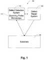
- FIG. 1is a high level schematic of a system according to one aspect of the present invention.
- FIG. 2is a schematic illustration of a system for locating and repairing defects in a workpiece according to one aspect of the present invention.
- FIG. 3is a schematic of a system for locating and repairing defects in a workpiece according to another aspect of the invention, illustrated in scan mode.
- FIG. 4is another schematic of the system of FIG. 3 , illustrated in defect repair mode.
- FIG. 5is a flow diagram of a process according to one aspect of the present invention.
- FIG. 1is a high level schematic of a system 100 according to one aspect of the present invention.
- System 100includes defect detection system 110 and defect repair system 120 , which may be combined in one apparatus.
- Defect detection system 10includes scanning probe microscope 112 .
- Defect repair system 120repairs defects in substrate 140 at locations determined by defect detection system 10 .
- Defect detection system 10may transfer a defect map to defect repair system 120 or, where the systems are combined, may repair defects using scanning probe microscope 112 . By combining defect repair with a scanning probe microscope's sensitive defect location ability, system 100 is able to carry out very precise repairs.
- a semiconductor substrateincludes a semiconducting material, such as silicon.
- the substratemay include various elements and/or layers; including metal layers, barrier layers, dielectric layers, device structures, active elements and passive elements including silicon gates, word lines, source regions, drain regions, bit lines, bases emitters, collectors, conductive lines, conductive plugs, etc.
- the substratemay have defects such as excess material or particulate contaminates.
- the scanning probe microscopemay be of any kind suitable for detecting defects in the substrate.
- the microscopemay be an atomic force microscope, a scanning tunneling microscope, or a scanning near-field optical microscope.
- the microscopemay make measurements based on any suitable short range interaction with the substrate surface, including forces such as Van der Waals, electrostatic, and magnetic, tunneling electrons, or evanescent photons.
- the microscopemay be operated in contact mode, non-contact mode, or tapping mode.
- the scanning probe microscopemay obtain topographical information, compositional information, material state information, or a combination of the forgoing such as compositional and topographical information.
- the scanning probe microscopemay also employ a combination of detection mechanisms.
- the microscopemay operate in both a contacting mode where displacement of the tip is caused by topographical features, and in a non-contacting mode where displacement of the tip is caused by electrostatic charges in the substrate induced by a conductive microscope tip.
- the detection limit of the microscopemay be in the range from about 0.1 nm to about 100 ⁇ m. In one aspect of the invention, the microscope has a detection limit in the range from about 1 nm to about 1 ⁇ m. In a further aspect of the invention, the scanning probe microscope has a detection limit in the range from about 10 nm to about 0.1 ⁇ m.
- the scanning probe microscopescans the substrate surface in search of defects.
- the SPMmay scan the entire surface or only selected portions thereof. For example, the SPM may only scan portions of the surface identified by a preliminary scan identifying potential defect location.
- the preliminary scanmay be carried out with a different scan technique, such as another SPM technique or with optical microscopy.
- a defectwhen a defect is found or suspected, the region where the defect is thought to be is scanned by the SPM to precisely locate the defect.
- defectsare detected using a combination of topographical and compositional information obtained using an SPM.
- defectsmay be recognized as soon as they are encountered by the SPM. Others may not be recognized until a region around the defect has been mapped. Accordingly, the repair operation may be initiated as soon as a defect is encountered or it may be postponed until a region of the surface has been mapped.
- Defectsare repaired at locations determined by the SPM.
- the SPMis positioned over the defect, or adjacent to it, and the SPM is used to repair the defect.
- the SPMis positioned over or near the defect and the defect is repaired by a separate tool that has a location fixed relative to the current position of the SPM.
- the defect location determined by the SPMis communicated to a separate defect repair system that repairs the defect at the location determined by the SPM.
- the repair toolcan be the same tip used to detect the defect. This is not only convenient, but ensures accuracy of the repair. On the other hand, very accurate repairs can be carried out using a separate structure, particularly one with fixed position relative to the scanning tip. Using a separate structure to repair the defect allows greater design flexibility in that the repair structure does not have to also be adapted for scanning.
- the repair structurecan be, for example, a tip for scribing the surface, a tip for applying an electric field to the surface, or a tip for heating the surface.
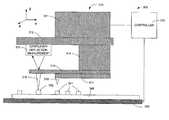
- FIG. 2schematically illustrates a scanning probe microscope system according to one aspect of the invention where the same scanning probe microscope tip is used to detect and repair defects.
- System 200includes atomic force microscope (AFM) 210 , controller 220 , and positioning table 230 .
- Controller 220operates AFM 210 and positioning table 230 to scan across substrate 240 in the X and Y directions.
- Positioning table 230may also provide for moving substrate 240 in the Z direction.
- AFM 210includes body 211 , scanning head 212 , deflection measuring system 213 , base 214 , cantilever 215 , and tip 216 .
- Body 211may provide for positioning scanning head 212 and the lower portions of AFM 210 in the Z direction.
- Deflection system 213measures the deflection of cantilever 215 caused by the interaction of tip 216 with the surface of substrate 240 , including features 241 and defect 242 .
- Body 211regulates the torque on cantilever 215 and the consequent normal force of tip 216 against the surface of substrate 240 .
- Controller 220which contains a microprocessor and memory programmed with software instructions, maps substrate 240 , or a portion thereof, into a grid wherein each portion of the grid corresponds to an XY position. Controller 240 directs position table 230 to move substrate 240 in a predetermined manner such that tip 216 scans across the surface of substrate 240 . At the location (X i , Y j ), AFM 210 detects a characteristic associated with the surface and converts the characteristic into one or more electrical signals, for example, analog signals or digital signals which represent the detected characteristic(s), and transmits the detected data to controller 240 .
- Controller 240analyzes the detected data according to its programming to determine a characteristic of the substrate surface at that location. Using such information from multiple locations on substrate 240 , controller 220 generates, for example, a map of the surface of substrate 240 including the location of any defects.
- system 200uses the surface map and additional readings from microscope 210 to reposition tip 216 over or adjacent the defect. The additional readings may be compared to the surface map to determine the location of tip 216 relative to the defect. Tip 216 is then used to repair the defect.
- AFM 210increases the normal force on tip 216 to the extent that when substrate 240 is moved in the X and/or Y direction, tip 216 scribes the surface of substrate 240 .
- the normal force used for locating defectsis, for example, from about 0.1 nN to about 20 nN. In one aspect of the invention, the normal force used for removing defects is at least about 10 times greater than the force used for locating defects.
- the normal force used for removing defectsis at least about 100 times greater than the force used for locating defects.
- the force useddepends on the material being scribed and may also be varied based on the amount of material that needs to be removed.
- the normal force used to scribe the surfaceis in the range from about 20 nN to about 2 ⁇ N. In another example, the normal force used is from about 100 nN to about 500 nN.
- Controller 220causes tip 216 to scribe across the location of the defect as many times as necessary to remove the defect. Data from tip 216 may be used to determined when defect removal is complete. During the scribing operation, controller 220 may vary the normal force on tip 216 to vary the depth to which the surface is scribed at different locations.
- tip 216includes a hard material suitable for scribing the substrate surface.
- tip 216may be provided with a diamond tip.
- defectsare repaired by switching on an electric field between substrate 240 and tip 216 .
- the electric fieldis applied by biasing substrate 240 to a first voltage and tip 216 to a second voltage.
- the voltage differencemay be in the range from about 1 V to about 100 V.
- the currentmay be in the range from about 0.1 nA to about 10 nA.
- tip 216is conductive, has a conductive coating, or includes a conductive strip.
- tip 216may have a strip of gold to which a voltage can be applied.
- the electric fieldcauses oxidation of the defect.
- the material removed from the substratemay be of a type that volatilizes upon oxidation. Alternatively, the material removed may be material that becomes more soluble in a solvent developer after oxidation and a developing step may be used to remove the oxidized material from the surface.
- tip 216may be heated by running a current through tip 216 .
- tip 116may include or comprise a metal wire through which a current may be run. Suitable metals may include platinum, silver, copper, and alloys of the forgoing such as a platinum/rhodium alloy.
- Another optionis to heat tip 216 with a laser focused on tip 216 .
- a pulsed laserprovides controlled doses of energy, although a continuous laser may also be used.
- tip 216may be provided with an absorbtive material such as a strip of gold. Heat from tip 216 may physically remove the defect or induce a chemical reaction that results in defect removed. Physical remove may include melting and/or vaporization. Chemical removal may include burning with oxygen.
- a suitable atmosphere around the scanning tipmay be provided to facilitate removal by a chemical reaction, such as burning.
- FIG. 3schematically illustrates a scanning probe microscope system that can be used to carry out the invention in one of its aspects wherein the scanning probe microscope has two tips, one for detection and the other for defect repair.
- System 300includes atomic force microscope (AFM) 310 , controller 320 , and positioning table 330 .
- AFM 310includes body 311 , scanning head 312 , deflection measuring system 313 , base 314 , measuring cantilever 315 , measuring tip 316 , scribing cantilever 317 , and scribing tip 318 .
- Deflection system 313measures the deflection of measuring cantilever 315 caused by the interaction of measuring tip 316 with the surface of substrate 340 , including features 341 and defect 342 .
- Body 330regulates the height of base 370 in the Z direction.
- System 300maps the surface of substrate 340 , for example in the same way that system 200 maps the surface of substrate 240 .
- scribing tip 318is further from the surface than measuring tip 316 and scribing tip 318 does not interact significantly with the surface.
- system 300uses the defect map and data from microscope measuring tip 316 to position scribing tip 318 over the defect. After moving measuring tip 316 to the approximate location of the defect, measuring tip 316 begins gathering data regarding the surface, and controller 320 correlates that data to previously gathered data to determine the location of the measuring tip relative to the defect. Once the location of the tip relative to the defect is determined, the measuring tip is guided to a position on or adjacent the defect such that the scribing tip is directly over or adjacent the defect. System 310 then closes the distance between the surface of substrate 340 and AFM 310 .
- measuring cantilever 315deflects away from the surface with the result that the relative difference in height above the surface of substrate 340 between measuring tip 316 and scribing tip 318 decreases.
- Cantilever 317is much more rigid than cantilever 315 such that once cantilever 315 has deflected to a sufficient degree, increases in the normal force exerted by microscope 310 against the surface of substrate 340 are exerted primarily through scribing tip 318 .
- Tip 318includes a hard material suitable for scribing the substrate surface.
- tip 318may include a diamond. Controller 340 causes scribing tip 318 to scribe across the location of the defect as many times as necessary to remove the defect. During this operation, data from measuring tip 316 may be used to determine when defect removal is complete.
- Repair operations of the inventionmay be facilitated by blowing a stream of ionized air against the substrate in the area of the defect.
- the ionized airmay neutralize charges and facilitate release of particulate debris from the surface and the flow of air may serve to convect the debris away from the surface.
- a vacuum systemmay also be provided to capture the blown debris and prevent it from contaminating the substrate or the environment in which the substrate is being processed.
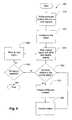
- FIG. 5is a flow diagram of a process 500 for repairing defects in a processed semiconductor substrate according to one aspect of the invention.
- the substrate surfaceis divided into regions.
- a regionis scanned using an SPM and defects within the region are identified. If there are defects in the region, the SPM is positioned over or adjacent the defect in step 570 . With the SPM positioned over or adjacent the defect, the defect is then removed in step 580 .
- the repair operationwith the scanning probe microscope's sensitive defect location system, very precise repairs can be carried out.
Landscapes
- Engineering & Computer Science (AREA)
- Manufacturing & Machinery (AREA)
- Computer Hardware Design (AREA)
- Microelectronics & Electronic Packaging (AREA)
- Power Engineering (AREA)
- Testing Or Measuring Of Semiconductors Or The Like (AREA)
Abstract
Description
This application claims the benefit of U.S. Provisional Patent Application Ser. No. 60/242,834, filed Oct. 24, 2000, entitled USED OF SCANNING PROBE MICROSCOPE FOR DEFECT DETECTION AND REPAIR.
The present invention generally relates to semiconductor processing, and in particular to a method of detecting and repairing defects in a semiconductor or other type of workpiece.
In the semiconductor industry, there is a continuing trend toward higher device densities. To achieve these high densities there have been, and continue to be, efforts toward scaling down the device dimensions on semiconductor wafers. In order to accomplish higher device density, smaller and smaller features sizes are required. These may include the width and spacing of interconnecting lines, spacing and diameter of contact holes, and surface geometry of corners and edges of various features.
High resolution lithographic processes are used to achieve small features. In general, lithography refers to processes for pattern transfer between various media. In lithography for integrated circuit fabrication, a silicon slice, the wafer, is coated uniformly with a radiation-sensitive film, the resist. The film is selectively exposed with radiation (such as optical light, x-rays, or an electron beam) through an intervening master template, the mask, forming a particular pattern. Exposed areas of the coating become either more or less soluble than the unexposed areas (depending on the type of coating) in a particular solvent developer. The more soluble areas are removed with the developer in a developing step. The less soluble areas remain on the silicon wafer forming a patterned coating. The pattern corresponds to the image of the mask or its negative. The patterned resist is used in further processing of the silicon wafer. Defects in the mask or the patterned resist may result in defects in the processed wafer.
In spite of advances in lithographic procedures, processed silicon wafers sometimes have defects, such as excess material or particulate contaminants. To improve quality, tools have been developed to detect such defects. One such tool, a scanning probe microscope, will detect many of the types of defects that can occur in processed silicon wafers.
Scanning probe microscopes come in several forms. One form is an Atomic Force Microscope (AFM), which is sometimes alternatively referred to as a Scanning Force Microscope (SFM). AFMs include a sensor with a spring-like cantilever rigidly mounted at one end and having a scanning tip at a free end. AFMs may operate in contacting and non-contacting modes. In the contacting mode, the tip of an AFM is placed in low force contact with a surface of a semiconductor wafer or other workpiece of interest. The workpiece is then displaced relative to the AFM in one or more directions in a plane (e.g., the tip contacts the workpiece in a Z axis while the workpiece is displaced in the X and/or Y directions), to effect a scanning of the workpiece surface. As surface contours or other topographic features are encountered by the tip during scanning, the cantilever deflects. The cantilever deflection is then measured, whereby the topography of the workpiece may be determined.
In non-contacting operation, the tip is held a short distance, typically 5 to 500 Angstroms, from the workpiece surface, and is deflected during scanning by various forces between the workpiece and the tip. Such forces may include magnetic, electrostatic, and van der Waals forces. In both the contacting and non-contacting modes, measurements of a workpiece topography or other characteristic features are obtained through measuring the deflection of the cantilever. Deflection of the cantilever may be measured using precisely aligned optical components coupled to deflection measurement circuitry, although other techniques are sometimes employed.
Another form of scanning probe microscope is a Scanning Tunneling Microscope (STM). Where a feature of interest is non-topographic, AFMs as well as STMs may be used to measure the workpiece feature. Examples of non-topographic features include the detection of variations in conductivity of a semiconductor workpiece material. An AFM can be used to scan a workpiece in the non-contacting mode during which deflections in the cantilever are caused by variations in the workpiece conductivity or other property of interest. The deflections can be measured to provide a measurement of the feature. STMs include a conductive scanning tip which is held in close proximity (within approximately 5 Angstroms) to the workpiece. At this distance, the probability density function of electrons on the tip spatially overlap the probability density function of atoms on the workpiece. Consequently, a tunneling current flows between the workpiece surface and the tip if a suitable bias voltage is applied between the tip and the workpiece. The workpiece and tip are relatively displaced horizontally (in the X and/or Y directions) while the tip is held a constant vertical distance from the workpiece surface. The variations in the current can be measured to determine the changes in the workpiece surface.
In another mode of operation, an STM can be used to measure topography. The scanner moves the tip up and down while scanning in the X and/or Y directions and sensing the tunneling current. The STM attempts to maintain the distance between the tip and the surface constant (through moving the tip vertically in response to measured current fluctuations). The movements of the tip up and down can be correlated to the surface topography profile of a workpiece.
While there has been significant progress in detecting defects, less progress has been made in repairing defects. Parts with defects may be discarded, but it would be advantageous if they could be reliably repaired. With the scaled down geometries of today's semiconductor devices, large wafers can have values, when fully processed, exceeding six figures. There is an unsatisfied need for a system and method of repairing defects in semiconductor devices with small features.
The present invention provides a system and method for detecting and repairing defects in semiconductor devices. According to the invention, defects are located using a scanning probe microscope, such as an atomic force microscope or a scanning tunneling microscope, and repaired at locations determined by the scanning probe microscope. The microscope itself, and in particular the detection tip, may be employed to remove the defects. For example, the tip may be used to machine away the defect, to apply an electric field to oxidize the defect, and/or to heat the defect causing it to burn or vaporize. By combining precise defect location capabilities of a scanning probe microscope with defect removal, the invention permits very precise correction of defects such as excess material and foreign particles on semiconductor substrates.
One aspect of the invention provides a system for repairing defects in a semiconductor substrate including a scanning probe microscope having a detection tip and a defect repair system, wherein the defect repair system repairs defects in a substrate at location determined by the scanning probe microscope.
Another aspect of the invention provides a system for repairing defects in a semiconductor substrate including a scanning probe microscope and means for selectively processing the semiconductor substrate to repair defects at locations on the semiconductor substrate determined by the scanning probe microscope.
A further aspect of the invention provides a method of repairing a defect in a semiconductor substrate including the steps of locating the defect using a scanning probe microscope and repairing the defect using the location determined by the scanning probe microscope.
The invention extends to features hereinafter fully described and features particularly pointed out in the claims. The following detailed description and the annexed drawings set forth in detail certain illustrative examples of the invention. These examples are indicative of but a few of the various ways in which the principles of the invention may be employed. Other ways in which the principles of the invention may be employed and other objects, advantages and novel features of the invention will be apparent from the detailed description of the invention when consider in conjunction with the drawings.
While the invention can be applied to any type of substrate, it is applied in particular to semiconductor substrates. A semiconductor substrate includes a semiconducting material, such as silicon. In addition to a semiconducting material, the substrate may include various elements and/or layers; including metal layers, barrier layers, dielectric layers, device structures, active elements and passive elements including silicon gates, word lines, source regions, drain regions, bit lines, bases emitters, collectors, conductive lines, conductive plugs, etc. The substrate may have defects such as excess material or particulate contaminates.
The scanning probe microscope may be of any kind suitable for detecting defects in the substrate. For example, the microscope may be an atomic force microscope, a scanning tunneling microscope, or a scanning near-field optical microscope. The microscope may make measurements based on any suitable short range interaction with the substrate surface, including forces such as Van der Waals, electrostatic, and magnetic, tunneling electrons, or evanescent photons. The microscope may be operated in contact mode, non-contact mode, or tapping mode. The scanning probe microscope may obtain topographical information, compositional information, material state information, or a combination of the forgoing such as compositional and topographical information. The scanning probe microscope may also employ a combination of detection mechanisms. For example, the microscope may operate in both a contacting mode where displacement of the tip is caused by topographical features, and in a non-contacting mode where displacement of the tip is caused by electrostatic charges in the substrate induced by a conductive microscope tip. The detection limit of the microscope may be in the range from about 0.1 nm to about 100 μm. In one aspect of the invention, the microscope has a detection limit in the range from about 1 nm to about 1 μm. In a further aspect of the invention, the scanning probe microscope has a detection limit in the range from about 10 nm to about 0.1 μm.
The scanning probe microscope scans the substrate surface in search of defects. The SPM may scan the entire surface or only selected portions thereof. For example, the SPM may only scan portions of the surface identified by a preliminary scan identifying potential defect location. The preliminary scan may be carried out with a different scan technique, such as another SPM technique or with optical microscopy. In one aspect of the invention, when a defect is found or suspected, the region where the defect is thought to be is scanned by the SPM to precisely locate the defect. In another aspect of the invention, defects are detected using a combination of topographical and compositional information obtained using an SPM.
Some types of defects may be recognized as soon as they are encountered by the SPM. Others may not be recognized until a region around the defect has been mapped. Accordingly, the repair operation may be initiated as soon as a defect is encountered or it may be postponed until a region of the surface has been mapped. Defects are repaired at locations determined by the SPM. In one aspect of the invention, the SPM is positioned over the defect, or adjacent to it, and the SPM is used to repair the defect. In another aspect of the invention, the SPM is positioned over or near the defect and the defect is repaired by a separate tool that has a location fixed relative to the current position of the SPM. In a further aspect of the invention, the defect location determined by the SPM is communicated to a separate defect repair system that repairs the defect at the location determined by the SPM.
The repair tool can be the same tip used to detect the defect. This is not only convenient, but ensures accuracy of the repair. On the other hand, very accurate repairs can be carried out using a separate structure, particularly one with fixed position relative to the scanning tip. Using a separate structure to repair the defect allows greater design flexibility in that the repair structure does not have to also be adapted for scanning. The repair structure can be, for example, a tip for scribing the surface, a tip for applying an electric field to the surface, or a tip for heating the surface.
The following is an example of howsystem 200 may operate to detect defects in the substrate surface topography and/or composition:Controller 220, which contains a microprocessor and memory programmed with software instructions, mapssubstrate 240, or a portion thereof, into a grid wherein each portion of the grid corresponds to an XY position.Controller 240 directs position table230 to movesubstrate 240 in a predetermined manner such thattip 216 scans across the surface ofsubstrate 240. At the location (Xi, Yj),AFM 210 detects a characteristic associated with the surface and converts the characteristic into one or more electrical signals, for example, analog signals or digital signals which represent the detected characteristic(s), and transmits the detected data tocontroller 240.Controller 240 analyzes the detected data according to its programming to determine a characteristic of the substrate surface at that location. Using such information from multiple locations onsubstrate 240,controller 220 generates, for example, a map of the surface ofsubstrate 240 including the location of any defects.
When defects are located,system 200 uses the surface map and additional readings frommicroscope 210 to repositiontip 216 over or adjacent the defect. The additional readings may be compared to the surface map to determine the location oftip 216 relative to the defect.Tip 216 is then used to repair the defect. In one example,AFM 210 increases the normal force ontip 216 to the extent that whensubstrate 240 is moved in the X and/or Y direction,tip 216 scribes the surface ofsubstrate 240. The normal force used for locating defects is, for example, from about 0.1 nN to about 20 nN. In one aspect of the invention, the normal force used for removing defects is at least about 10 times greater than the force used for locating defects. In another aspect of the invention, the normal force used for removing defects is at least about 100 times greater than the force used for locating defects. The force used depends on the material being scribed and may also be varied based on the amount of material that needs to be removed. In one example, the normal force used to scribe the surface is in the range from about 20 nN to about 2 μN. In another example, the normal force used is from about 100 nN to about 500 nN.Controller 220 causestip 216 to scribe across the location of the defect as many times as necessary to remove the defect. Data fromtip 216 may be used to determined when defect removal is complete. During the scribing operation,controller 220 may vary the normal force ontip 216 to vary the depth to which the surface is scribed at different locations. In this example,tip 216 includes a hard material suitable for scribing the substrate surface. For example,tip 216 may be provided with a diamond tip.
In another aspect of the invention, defects are repaired by switching on an electric field betweensubstrate 240 andtip 216. The electric field is applied by biasingsubstrate 240 to a first voltage andtip 216 to a second voltage. As an example, the voltage difference may be in the range from about 1 V to about 100 V. By way of further example, the current may be in the range from about 0.1 nA to about 10 nA. In this aspect of the invention,tip 216 is conductive, has a conductive coating, or includes a conductive strip. For example,tip 216 may have a strip of gold to which a voltage can be applied. The electric field causes oxidation of the defect. The material removed from the substrate may be of a type that volatilizes upon oxidation. Alternatively, the material removed may be material that becomes more soluble in a solvent developer after oxidation and a developing step may be used to remove the oxidized material from the surface.
In a further aspect of the invention, defects are repaired byheating tip 216.Tip 216 may be heated by running a current throughtip 216. For example, tip116 may include or comprise a metal wire through which a current may be run. Suitable metals may include platinum, silver, copper, and alloys of the forgoing such as a platinum/rhodium alloy. Another option is to heattip 216 with a laser focused ontip 216. A pulsed laser provides controlled doses of energy, although a continuous laser may also be used. To facilitate laser heating,tip 216 may be provided with an absorbtive material such as a strip of gold. Heat fromtip 216 may physically remove the defect or induce a chemical reaction that results in defect removed. Physical remove may include melting and/or vaporization. Chemical removal may include burning with oxygen. A suitable atmosphere around the scanning tip may be provided to facilitate removal by a chemical reaction, such as burning.
When defects are located,system 300 uses the defect map and data frommicroscope measuring tip 316 to positionscribing tip 318 over the defect. After moving measuringtip 316 to the approximate location of the defect, measuringtip 316 begins gathering data regarding the surface, andcontroller 320 correlates that data to previously gathered data to determine the location of the measuring tip relative to the defect. Once the location of the tip relative to the defect is determined, the measuring tip is guided to a position on or adjacent the defect such that the scribing tip is directly over or adjacent the defect.System 310 then closes the distance between the surface ofsubstrate 340 andAFM 310.
As illustrated byFIG. 4 , closing the distance betweenAFM 310 andsubstrate 340 causes the normal force on measuringcantilever 315 to increase. Measuringcantilever 315 deflects away from the surface with the result that the relative difference in height above the surface ofsubstrate 340 between measuringtip 316 andscribing tip 318 decreases.Cantilever 317 is much more rigid thancantilever 315 such that oncecantilever 315 has deflected to a sufficient degree, increases in the normal force exerted bymicroscope 310 against the surface ofsubstrate 340 are exerted primarily throughscribing tip 318.Tip 318 includes a hard material suitable for scribing the substrate surface. For example,tip 318 may include a diamond.Controller 340causes scribing tip 318 to scribe across the location of the defect as many times as necessary to remove the defect. During this operation, data from measuringtip 316 may be used to determine when defect removal is complete.
Repair operations of the invention, particularly those involving mechanical scribing of a substrate, may be facilitated by blowing a stream of ionized air against the substrate in the area of the defect. The ionized air may neutralize charges and facilitate release of particulate debris from the surface and the flow of air may serve to convect the debris away from the surface. A vacuum system may also be provided to capture the blown debris and prevent it from contaminating the substrate or the environment in which the substrate is being processed.
What has been described above is the present invention and several of its specific embodiments. It is, of course, not possible to describe every conceivable combination of components or methodologies for purposes of describing the present invention, but one of ordinary skill in the art will recognize that many further combinations and permutations of the present invention are possible. Accordingly, the present invention is intended to embrace all such alterations, modifications and variations that fall within the spirit and scope of the appended claims.
Claims (21)
1. A system for repairing defects in a semiconductor substrate, comprising:
a scanning probe microscope that has a measuring tip and a scribing tip; and
a defect repair system that repairs defects in a substrate via application of a first voltage to the substrate and a second voltage to the scribing tip, which is positioned at a location determined by the scanning probe microscope;
wherein defect location(s) and the substrate itself are mapped into a grid, each portion of which corresponds to an XY position.
2. The system ofclaim 1 , wherein the defects are mechanically removed from the substrate using the scribing tip.
3. The system ofclaim 2 , wherein the scanning probe microscope is an atomic force microscope.
4. The method ofclaim 3 , wherein the scribing tip of the scanning probe microscope has a diamond tip.
5. The system ofclaim 1 , wherein the voltage difference causes defects to be oxidized away.
6. The system ofclaim 1 , wherein the defects are repaired by heating the scribing tip.
7. The system ofclaim 1 , wherein the system locates defects by obtaining both topographical and compositional information concerning the substrate.
8. The system ofclaim 7 , wherein the system creates an electrostatic charge in a portion of the substrate.
9. The system ofclaim 1 , wherein the measuring tip has fixed position relative to the scribing tip of the scanning probe microscope.
10. The system ofclaim 1 , wherein the defect repair system receives a defect map generated using the scanning probe microscope.
11. A system for repairing defects in a semiconductor substrate, comprising:
a scanning probe microscope that has a measuring tip and a scribing tip;
means for selectively processing the semiconductor substrate to repair defects at locations on the semiconductor substrate determined by the scanning probe microscope;
means for applying a first biasing voltage to the semiconductor substrate and a second biasing voltage to the scribing tip; and
means for mapping the semiconductor substrate and defect locations thereon in a grid pattern.
12. A method of repairing a defect in a semiconductor substrate comprising:
locating the defect via employing a measuring tip of a scanning probe microscope;
mapping the defect location to XY coordinates in a grid map of the semiconductor substrate; and
repairing the defect at the location determined by the scanning probe microscope measuring tip via employing a scribing tip, wherein a first biasing voltage is applied to the semiconductor substrate and a second biasing voltage is applied to the scribing tip.
13. The method ofclaim 12 , wherein the defect is mechanically removed from the substrate using the scribing tip.
14. The method ofclaim 13 , wherein the scanning probe microscope is an atomic force microscope.
15. The method ofclaim 14 , wherein the scribing tip of the scanning probe microscope has a diamond tip.
16. The method ofclaim 13 , wherein the defect is removed by forcing the tip against the substrate with a normal force that is at least about ten times greater than the normal force applied to detect the defect.
17. The method ofclaim 12 , wherein the voltage difference causes the defect to be oxidized away.
18. The method ofclaim 12 , wherein the step of repairing the defect comprises heating the scribing tip.
19. The method ofclaim 12 , is further comprising the step of determining the approximate location of the defect with another instrument prior to the step of determining the defect's location using the scanning probe microscope.
20. The method ofclaim 12 , wherein the step of locating the defect comprises obtains both topographical and compositional information regarding the substrate.
21. The method ofclaim 20 , wherein the step of locating the defect comprising creating an electrostatic charge in a portion of the substrate.
Priority Applications (1)
| Application Number | Priority Date | Filing Date | Title |
|---|---|---|---|
| US09/729,513US6884999B1 (en) | 2000-10-24 | 2000-12-04 | Use of scanning probe microscope for defect detection and repair |
Applications Claiming Priority (2)
| Application Number | Priority Date | Filing Date | Title |
|---|---|---|---|
| US24283400P | 2000-10-24 | 2000-10-24 | |
| US09/729,513US6884999B1 (en) | 2000-10-24 | 2000-12-04 | Use of scanning probe microscope for defect detection and repair |
Publications (1)
| Publication Number | Publication Date |
|---|---|
| US6884999B1true US6884999B1 (en) | 2005-04-26 |
Family
ID=34437178
Family Applications (1)
| Application Number | Title | Priority Date | Filing Date |
|---|---|---|---|
| US09/729,513Expired - Fee RelatedUS6884999B1 (en) | 2000-10-24 | 2000-12-04 | Use of scanning probe microscope for defect detection and repair |
Country Status (1)
| Country | Link |
|---|---|
| US (1) | US6884999B1 (en) |
Cited By (19)
| Publication number | Priority date | Publication date | Assignee | Title |
|---|---|---|---|---|
| US20020189330A1 (en)* | 2001-03-30 | 2002-12-19 | Vladimir Mancevski | Caliper method, system, and apparatus |
| US20040257380A1 (en)* | 2003-06-20 | 2004-12-23 | Herbert Leslie B. | Imaging method and system |
| US20050199809A1 (en)* | 2004-03-15 | 2005-09-15 | Shigeru Wakiyama | Processing probe |
| JP2005297185A (en)* | 2004-04-15 | 2005-10-27 | Fei Co | Stylus system for correcting micro-structure |
| US20050269035A1 (en)* | 2004-06-07 | 2005-12-08 | Eigo Kawakami | Fine pattern forming apparatus and fine pattern inspecting apparatus |
| US20050281174A1 (en)* | 2004-06-22 | 2005-12-22 | International Business Machines Corporation | Data storage device and control |
| US20060007433A1 (en)* | 2004-07-08 | 2006-01-12 | Asahi Glass Company Ltd. | Defect repair device and defect repair method |
| US20060011830A1 (en)* | 2002-08-30 | 2006-01-19 | Yoshiharu Shirakawabe | Method of manufacturing the multi-tip probe, a multi-tip probe, and surface characteristic analysis apparatus |
| US20060242820A1 (en)* | 2002-12-10 | 2006-11-02 | Steve Townsend | Automated pallet inspection and repair |
| US20070010032A1 (en)* | 2004-05-14 | 2007-01-11 | Patterson Oliver D | Defect identification system and method for repairing killer defects in semiconductor devices |
| US20070012094A1 (en)* | 2005-06-17 | 2007-01-18 | Degertekin F L | Integrated displacement sensors for probe microscopy and force spectroscopy |
| US20070227236A1 (en)* | 2006-03-13 | 2007-10-04 | Bonilla Flavio A | Nanoindenter |
| US20080073522A1 (en)* | 2006-03-20 | 2008-03-27 | Osamu Takaoka | Method of correcting opaque defect of chrome mask, in which atomic force microscope fine working apparatus has been used |
| WO2008099316A1 (en) | 2007-02-13 | 2008-08-21 | Philips Intellectual Property & Standards Gmbh | Defect treatment apparatus |
| JP2009172703A (en)* | 2008-01-23 | 2009-08-06 | Seiko Instruments Inc | Probe for micromachining device and micromachining device |
| US20210151305A1 (en)* | 2018-04-20 | 2021-05-20 | Shimadzu Research Laboratory(Shanghai) Co. Ltd. | Ionization device, mass spectrometer, ion mobility spectrometer, and ionization method |
| CN113252947A (en)* | 2021-04-21 | 2021-08-13 | 上海交通大学 | Multi-probe-based non-light-source type near-field thermal radiation scanning microscope system |
| US20230417795A1 (en)* | 2022-06-16 | 2023-12-28 | University Of Central Florida Research Foundation, Inc. | Controlled creation of sub-50 nm defects in 2d materials at low temperature |
| US12001145B2 (en)* | 2018-05-18 | 2024-06-04 | Carl Zeiss Smt Gmbh | Apparatus and method for analyzing an element of a photolithography process with the aid of a transformation model |
Citations (17)
| Publication number | Priority date | Publication date | Assignee | Title |
|---|---|---|---|---|
| US4747698A (en)* | 1986-04-30 | 1988-05-31 | International Business Machines Corp. | Scanning thermal profiler |
| US4896044A (en)* | 1989-02-17 | 1990-01-23 | Purdue Research Foundation | Scanning tunneling microscope nanoetching method |
| US5356218A (en)* | 1993-05-04 | 1994-10-18 | Motorola, Inc. | Probe for providing surface images |
| US5546374A (en)* | 1993-09-29 | 1996-08-13 | Canon Kabushiki Kaisha | Information recording and/or reproducing apparatus using probe |
| US5618760A (en) | 1994-04-12 | 1997-04-08 | The Board Of Trustees Of The Leland Stanford, Jr. University | Method of etching a pattern on a substrate using a scanning probe microscope |
| US5627815A (en)* | 1992-09-14 | 1997-05-06 | Hitachi, Ltd. | Precision machining method precision machining apparatus and data storage apparatus using the same |
| US5666190A (en)* | 1994-04-12 | 1997-09-09 | The Board Of Trustees Of The Leland Stanford, Jr. University | Method of performing lithography using cantilever array |
| US5702849A (en)* | 1993-12-09 | 1997-12-30 | Mitsubishi Denki Kabushiki Kaisha | Mask for transferring a pattern for use in a semiconductor device and method of manufacturing the same |
| US5866807A (en)* | 1997-02-04 | 1999-02-02 | Digital Instruments | Method and apparatus for measuring mechanical properties on a small scale |
| US5865978A (en)* | 1997-05-09 | 1999-02-02 | Cohen; Adam E. | Near-field photolithographic masks and photolithography; nanoscale patterning techniques; apparatus and method therefor |
| US5966677A (en) | 1997-02-28 | 1999-10-12 | Fiekowsky; Peter J. | High accuracy particle dimension measurement system |
| US6000947A (en) | 1994-04-12 | 1999-12-14 | The Board Of Trustees Of The Leland Stanford, Jr. | Method of fabricating transistor or other electronic device using scanning probe microscope |
| US6181097B1 (en)* | 1999-02-11 | 2001-01-30 | Institute Of Materials Research And Engineering | High precision three-dimensional alignment system for lithography, fabrication and inspection |
| US6197455B1 (en)* | 1999-01-14 | 2001-03-06 | Advanced Micro Devices, Inc. | Lithographic mask repair using a scanning tunneling microscope |
| US6232597B1 (en)* | 1994-07-28 | 2001-05-15 | General Nanotechnology, Llc | Scanning probe microscope assembly and method for making confocal, spectrophotometric, near-field, and scanning probe measurements and associated images |
| US6366340B1 (en)* | 1995-08-18 | 2002-04-02 | Hitachi, Ltd. | Electron exposure apparatus |
| US20020104963A1 (en)* | 1998-09-26 | 2002-08-08 | Vladimir Mancevski | Multidimensional sensing system for atomic force microscopy |
- 2000
- 2000-12-04USUS09/729,513patent/US6884999B1/ennot_activeExpired - Fee Related
Patent Citations (17)
| Publication number | Priority date | Publication date | Assignee | Title |
|---|---|---|---|---|
| US4747698A (en)* | 1986-04-30 | 1988-05-31 | International Business Machines Corp. | Scanning thermal profiler |
| US4896044A (en)* | 1989-02-17 | 1990-01-23 | Purdue Research Foundation | Scanning tunneling microscope nanoetching method |
| US5627815A (en)* | 1992-09-14 | 1997-05-06 | Hitachi, Ltd. | Precision machining method precision machining apparatus and data storage apparatus using the same |
| US5356218A (en)* | 1993-05-04 | 1994-10-18 | Motorola, Inc. | Probe for providing surface images |
| US5546374A (en)* | 1993-09-29 | 1996-08-13 | Canon Kabushiki Kaisha | Information recording and/or reproducing apparatus using probe |
| US5702849A (en)* | 1993-12-09 | 1997-12-30 | Mitsubishi Denki Kabushiki Kaisha | Mask for transferring a pattern for use in a semiconductor device and method of manufacturing the same |
| US6000947A (en) | 1994-04-12 | 1999-12-14 | The Board Of Trustees Of The Leland Stanford, Jr. | Method of fabricating transistor or other electronic device using scanning probe microscope |
| US5618760A (en) | 1994-04-12 | 1997-04-08 | The Board Of Trustees Of The Leland Stanford, Jr. University | Method of etching a pattern on a substrate using a scanning probe microscope |
| US5666190A (en)* | 1994-04-12 | 1997-09-09 | The Board Of Trustees Of The Leland Stanford, Jr. University | Method of performing lithography using cantilever array |
| US6232597B1 (en)* | 1994-07-28 | 2001-05-15 | General Nanotechnology, Llc | Scanning probe microscope assembly and method for making confocal, spectrophotometric, near-field, and scanning probe measurements and associated images |
| US6366340B1 (en)* | 1995-08-18 | 2002-04-02 | Hitachi, Ltd. | Electron exposure apparatus |
| US5866807A (en)* | 1997-02-04 | 1999-02-02 | Digital Instruments | Method and apparatus for measuring mechanical properties on a small scale |
| US5966677A (en) | 1997-02-28 | 1999-10-12 | Fiekowsky; Peter J. | High accuracy particle dimension measurement system |
| US5865978A (en)* | 1997-05-09 | 1999-02-02 | Cohen; Adam E. | Near-field photolithographic masks and photolithography; nanoscale patterning techniques; apparatus and method therefor |
| US20020104963A1 (en)* | 1998-09-26 | 2002-08-08 | Vladimir Mancevski | Multidimensional sensing system for atomic force microscopy |
| US6197455B1 (en)* | 1999-01-14 | 2001-03-06 | Advanced Micro Devices, Inc. | Lithographic mask repair using a scanning tunneling microscope |
| US6181097B1 (en)* | 1999-02-11 | 2001-01-30 | Institute Of Materials Research And Engineering | High precision three-dimensional alignment system for lithography, fabrication and inspection |
Non-Patent Citations (2)
| Title |
|---|
| Mango, R. and Bennett, B.R.; "Nanostructure Patterns Written in III-V Semiconductors by an Atomic Force Microscope", Applied Physics; Apr. 7, 1997, American Institute of Physics, vol. 70, No. 14, pp. 1855-1857. |
| Sugimura, H., et al., "Maskless Patterning of Silicon Surface Based on Scanning Tunneling Microscope Tip-Induced Anodization and Chemical Etching", Applied Physics; Sep. 19, 1994, American Institute of Physics, vol. 65, No. 12, pp. 1569-1571. |
Cited By (38)
| Publication number | Priority date | Publication date | Assignee | Title |
|---|---|---|---|---|
| US20060037379A1 (en)* | 2001-03-30 | 2006-02-23 | Vladimar Mancevski | Caliper method, system, and apparatus |
| US7493794B2 (en)* | 2001-03-30 | 2009-02-24 | Xidex Corporation | Method of calibrating a caliper AFM |
| US20080078229A1 (en)* | 2001-03-30 | 2008-04-03 | Vladimir Mancevski | Caliper method, system, and apparatus |
| US6955078B2 (en)* | 2001-03-30 | 2005-10-18 | Xidex Corporation | Caliper method, system, and apparatus |
| US20020189330A1 (en)* | 2001-03-30 | 2002-12-19 | Vladimir Mancevski | Caliper method, system, and apparatus |
| US7337656B2 (en)* | 2002-08-30 | 2008-03-04 | Sii Nanotechnology Inc. | Surface characteristic analysis apparatus |
| US20060011830A1 (en)* | 2002-08-30 | 2006-01-19 | Yoshiharu Shirakawabe | Method of manufacturing the multi-tip probe, a multi-tip probe, and surface characteristic analysis apparatus |
| US7765668B2 (en)* | 2002-12-10 | 2010-08-03 | Chep Technology Pty Limited | Automated pallet inspection and repair |
| US20060242820A1 (en)* | 2002-12-10 | 2006-11-02 | Steve Townsend | Automated pallet inspection and repair |
| US20040257380A1 (en)* | 2003-06-20 | 2004-12-23 | Herbert Leslie B. | Imaging method and system |
| US7308158B2 (en)* | 2003-06-20 | 2007-12-11 | Eastman Kodak Company | Imaging method and system |
| US7378654B2 (en)* | 2004-03-15 | 2008-05-27 | Sii Nanotechnology Inc. | Processing probe |
| US20050199809A1 (en)* | 2004-03-15 | 2005-09-15 | Shigeru Wakiyama | Processing probe |
| JP2005297185A (en)* | 2004-04-15 | 2005-10-27 | Fei Co | Stylus system for correcting micro-structure |
| US20050266586A1 (en)* | 2004-04-15 | 2005-12-01 | Robert Linder | Stylus system for modifying small structures |
| US7375324B2 (en)* | 2004-04-15 | 2008-05-20 | Fei Company | Stylus system for modifying small structures |
| US7547560B2 (en)* | 2004-05-14 | 2009-06-16 | Agere Systems Inc. | Defect identification system and method for repairing killer defects in semiconductor devices |
| US20070010032A1 (en)* | 2004-05-14 | 2007-01-11 | Patterson Oliver D | Defect identification system and method for repairing killer defects in semiconductor devices |
| US7196321B2 (en)* | 2004-06-07 | 2007-03-27 | Canon Kabushiki Kaisha | Fine pattern forming apparatus and fine pattern inspecting apparatus |
| US20050269035A1 (en)* | 2004-06-07 | 2005-12-08 | Eigo Kawakami | Fine pattern forming apparatus and fine pattern inspecting apparatus |
| US20050281174A1 (en)* | 2004-06-22 | 2005-12-22 | International Business Machines Corporation | Data storage device and control |
| US7675837B2 (en)* | 2004-06-22 | 2010-03-09 | International Business Machines Corporation | Device and method for mechanical data storage device operation and control |
| US20080225676A1 (en)* | 2004-06-22 | 2008-09-18 | Gotsman Bernd W | Data storage device and control |
| US7522511B2 (en)* | 2004-06-22 | 2009-04-21 | International Business Machines Corporation | Method for mechanical data storage device operation and control |
| US7230695B2 (en)* | 2004-07-08 | 2007-06-12 | Asahi Glass Company, Ltd. | Defect repair device and defect repair method |
| US20060007433A1 (en)* | 2004-07-08 | 2006-01-12 | Asahi Glass Company Ltd. | Defect repair device and defect repair method |
| US7637149B2 (en)* | 2005-06-17 | 2009-12-29 | Georgia Tech Research Corporation | Integrated displacement sensors for probe microscopy and force spectroscopy |
| US20070012094A1 (en)* | 2005-06-17 | 2007-01-18 | Degertekin F L | Integrated displacement sensors for probe microscopy and force spectroscopy |
| US7685869B2 (en) | 2006-03-13 | 2010-03-30 | Asylum Research Corporation | Nanoindenter |
| US20070227236A1 (en)* | 2006-03-13 | 2007-10-04 | Bonilla Flavio A | Nanoindenter |
| US20080073522A1 (en)* | 2006-03-20 | 2008-03-27 | Osamu Takaoka | Method of correcting opaque defect of chrome mask, in which atomic force microscope fine working apparatus has been used |
| WO2008099316A1 (en) | 2007-02-13 | 2008-08-21 | Philips Intellectual Property & Standards Gmbh | Defect treatment apparatus |
| JP2009172703A (en)* | 2008-01-23 | 2009-08-06 | Seiko Instruments Inc | Probe for micromachining device and micromachining device |
| US20210151305A1 (en)* | 2018-04-20 | 2021-05-20 | Shimadzu Research Laboratory(Shanghai) Co. Ltd. | Ionization device, mass spectrometer, ion mobility spectrometer, and ionization method |
| US11735407B2 (en)* | 2018-04-20 | 2023-08-22 | Shimadzu Research Laboratory (Shanghai) Co. Ltd. | Ionization device, mass spectrometer, ion mobility spectrometer, and ionization method |
| US12001145B2 (en)* | 2018-05-18 | 2024-06-04 | Carl Zeiss Smt Gmbh | Apparatus and method for analyzing an element of a photolithography process with the aid of a transformation model |
| CN113252947A (en)* | 2021-04-21 | 2021-08-13 | 上海交通大学 | Multi-probe-based non-light-source type near-field thermal radiation scanning microscope system |
| US20230417795A1 (en)* | 2022-06-16 | 2023-12-28 | University Of Central Florida Research Foundation, Inc. | Controlled creation of sub-50 nm defects in 2d materials at low temperature |
Similar Documents
| Publication | Publication Date | Title |
|---|---|---|
| US6884999B1 (en) | Use of scanning probe microscope for defect detection and repair | |
| US11733186B2 (en) | Device and method for analyzing a defect of a photolithographic mask or of a wafer | |
| US6953519B2 (en) | Method of manufacturing the multi-tip probe, a multi-tip probe, and surface characteristic analysis apparatus | |
| JP5337974B2 (en) | Stylus system for modifying microstructures | |
| WO2004074816A1 (en) | Scanning probe microscope and sample observing method using this and semiconductor device production method | |
| WO2000020823A2 (en) | Atomic force microscope for profiling high aspect ratio samples | |
| JP3925380B2 (en) | Scanning probe microscope | |
| TWI729418B (en) | Apparatus and method for examining and/or processing a sample | |
| US6000281A (en) | Method and apparatus for measuring critical dimensions on a semiconductor surface | |
| Olbrich et al. | High aspect ratio all diamond tips formed by focused ion beam for conducting atomic force microscopy | |
| US6181097B1 (en) | High precision three-dimensional alignment system for lithography, fabrication and inspection | |
| TW202030762A (en) | Apparatus and method for determining a position of an element on a photolithographic mask | |
| US20060238206A1 (en) | Measuring system for the combined scanning and analysis of microtechnical components comprising electrical contacts | |
| US6545273B1 (en) | Use of multiple tips on AFM to deconvolve tip effects | |
| CN110526203A (en) | Method based on the quasi- three-dimensional micro-nano structure of AFM write-through stress-electric coupling lithography | |
| US6614243B2 (en) | Measurement probe for detecting electrical signals in an integrated semiconductor circuit | |
| US6455847B1 (en) | Carbon nanotube probes in atomic force microscope to detect partially open/closed contacts | |
| JP5048455B2 (en) | Photomask defect correction apparatus and method | |
| US20080131792A1 (en) | Method of Correcting Photomask Defect | |
| Birkelund et al. | New approaches to atomic force microscope lithography on silicon | |
| US6057914A (en) | Method for detecting and identifying a lens aberration by measurement of sidewall angles by atomic force microscopy | |
| US20240133919A1 (en) | Method of removing and collecting particles from photomask and device for removing and collecting particles therefrom | |
| JPH07192985A (en) | Pattern forming method and apparatus | |
| US20250251420A1 (en) | Method for inspecting semiconductor manufacturing equipment using a wafer | |
| US8327461B2 (en) | High-speed scanning probe microscope |
Legal Events
| Date | Code | Title | Description |
|---|---|---|---|
| AS | Assignment | Owner name:ADVANCED MICRO DEVICES, CALIFORNIA Free format text:ASSIGNMENT OF ASSIGNORS INTEREST;ASSIGNORS:YEDUR, SANJAY K.;SINGH, BHANWAR;CHOO, BRYAN K.;REEL/FRAME:011322/0701;SIGNING DATES FROM 20000926 TO 20001127 | |
| FPAY | Fee payment | Year of fee payment:4 | |
| AS | Assignment | Owner name:GLOBALFOUNDRIES INC., CAYMAN ISLANDS Free format text:AFFIRMATION OF PATENT ASSIGNMENT;ASSIGNOR:ADVANCED MICRO DEVICES, INC.;REEL/FRAME:023119/0083 Effective date:20090630 | |
| FPAY | Fee payment | Year of fee payment:8 | |
| REMI | Maintenance fee reminder mailed | ||
| LAPS | Lapse for failure to pay maintenance fees | ||
| STCH | Information on status: patent discontinuation | Free format text:PATENT EXPIRED DUE TO NONPAYMENT OF MAINTENANCE FEES UNDER 37 CFR 1.362 | |
| FP | Expired due to failure to pay maintenance fee | Effective date:20170426 | |
| AS | Assignment | Owner name:GLOBALFOUNDRIES U.S. INC., NEW YORK Free format text:RELEASE BY SECURED PARTY;ASSIGNOR:WILMINGTON TRUST, NATIONAL ASSOCIATION;REEL/FRAME:056987/0001 Effective date:20201117 |