US6884739B2 - Lanthanide doped TiOx dielectric films by plasma oxidation - Google Patents
Lanthanide doped TiOx dielectric films by plasma oxidationDownload PDFInfo
- Publication number
- US6884739B2 US6884739B2US10/219,870US21987002AUS6884739B2US 6884739 B2US6884739 B2US 6884739B2US 21987002 AUS21987002 AUS 21987002AUS 6884739 B2US6884739 B2US 6884739B2
- Authority
- US
- United States
- Prior art keywords
- lanthanide
- rate
- film
- evaporating
- substrate
- Prior art date
- Legal status (The legal status is an assumption and is not a legal conclusion. Google has not performed a legal analysis and makes no representation as to the accuracy of the status listed.)
- Expired - Lifetime
Links
Images


Classifications
- H—ELECTRICITY
- H01—ELECTRIC ELEMENTS
- H01L—SEMICONDUCTOR DEVICES NOT COVERED BY CLASS H10
- H01L21/00—Processes or apparatus adapted for the manufacture or treatment of semiconductor or solid state devices or of parts thereof
- H01L21/02—Manufacture or treatment of semiconductor devices or of parts thereof
- H01L21/02104—Forming layers
- H01L21/02107—Forming insulating materials on a substrate
- H01L21/02225—Forming insulating materials on a substrate characterised by the process for the formation of the insulating layer
- H01L21/02227—Forming insulating materials on a substrate characterised by the process for the formation of the insulating layer formation by a process other than a deposition process
- H01L21/0223—Forming insulating materials on a substrate characterised by the process for the formation of the insulating layer formation by a process other than a deposition process formation by oxidation, e.g. oxidation of the substrate
- H01L21/02244—Forming insulating materials on a substrate characterised by the process for the formation of the insulating layer formation by a process other than a deposition process formation by oxidation, e.g. oxidation of the substrate of a metallic layer
- C—CHEMISTRY; METALLURGY
- C23—COATING METALLIC MATERIAL; COATING MATERIAL WITH METALLIC MATERIAL; CHEMICAL SURFACE TREATMENT; DIFFUSION TREATMENT OF METALLIC MATERIAL; COATING BY VACUUM EVAPORATION, BY SPUTTERING, BY ION IMPLANTATION OR BY CHEMICAL VAPOUR DEPOSITION, IN GENERAL; INHIBITING CORROSION OF METALLIC MATERIAL OR INCRUSTATION IN GENERAL
- C23C—COATING METALLIC MATERIAL; COATING MATERIAL WITH METALLIC MATERIAL; SURFACE TREATMENT OF METALLIC MATERIAL BY DIFFUSION INTO THE SURFACE, BY CHEMICAL CONVERSION OR SUBSTITUTION; COATING BY VACUUM EVAPORATION, BY SPUTTERING, BY ION IMPLANTATION OR BY CHEMICAL VAPOUR DEPOSITION, IN GENERAL
- C23C14/00—Coating by vacuum evaporation, by sputtering or by ion implantation of the coating forming material
- C23C14/06—Coating by vacuum evaporation, by sputtering or by ion implantation of the coating forming material characterised by the coating material
- C23C14/14—Metallic material, boron or silicon
- C—CHEMISTRY; METALLURGY
- C23—COATING METALLIC MATERIAL; COATING MATERIAL WITH METALLIC MATERIAL; CHEMICAL SURFACE TREATMENT; DIFFUSION TREATMENT OF METALLIC MATERIAL; COATING BY VACUUM EVAPORATION, BY SPUTTERING, BY ION IMPLANTATION OR BY CHEMICAL VAPOUR DEPOSITION, IN GENERAL; INHIBITING CORROSION OF METALLIC MATERIAL OR INCRUSTATION IN GENERAL
- C23C—COATING METALLIC MATERIAL; COATING MATERIAL WITH METALLIC MATERIAL; SURFACE TREATMENT OF METALLIC MATERIAL BY DIFFUSION INTO THE SURFACE, BY CHEMICAL CONVERSION OR SUBSTITUTION; COATING BY VACUUM EVAPORATION, BY SPUTTERING, BY ION IMPLANTATION OR BY CHEMICAL VAPOUR DEPOSITION, IN GENERAL
- C23C14/00—Coating by vacuum evaporation, by sputtering or by ion implantation of the coating forming material
- C23C14/22—Coating by vacuum evaporation, by sputtering or by ion implantation of the coating forming material characterised by the process of coating
- C23C14/54—Controlling or regulating the coating process
- C23C14/548—Controlling the composition
- C—CHEMISTRY; METALLURGY
- C23—COATING METALLIC MATERIAL; COATING MATERIAL WITH METALLIC MATERIAL; CHEMICAL SURFACE TREATMENT; DIFFUSION TREATMENT OF METALLIC MATERIAL; COATING BY VACUUM EVAPORATION, BY SPUTTERING, BY ION IMPLANTATION OR BY CHEMICAL VAPOUR DEPOSITION, IN GENERAL; INHIBITING CORROSION OF METALLIC MATERIAL OR INCRUSTATION IN GENERAL
- C23C—COATING METALLIC MATERIAL; COATING MATERIAL WITH METALLIC MATERIAL; SURFACE TREATMENT OF METALLIC MATERIAL BY DIFFUSION INTO THE SURFACE, BY CHEMICAL CONVERSION OR SUBSTITUTION; COATING BY VACUUM EVAPORATION, BY SPUTTERING, BY ION IMPLANTATION OR BY CHEMICAL VAPOUR DEPOSITION, IN GENERAL
- C23C14/00—Coating by vacuum evaporation, by sputtering or by ion implantation of the coating forming material
- C23C14/58—After-treatment
- C23C14/5826—Treatment with charged particles
- C—CHEMISTRY; METALLURGY
- C23—COATING METALLIC MATERIAL; COATING MATERIAL WITH METALLIC MATERIAL; CHEMICAL SURFACE TREATMENT; DIFFUSION TREATMENT OF METALLIC MATERIAL; COATING BY VACUUM EVAPORATION, BY SPUTTERING, BY ION IMPLANTATION OR BY CHEMICAL VAPOUR DEPOSITION, IN GENERAL; INHIBITING CORROSION OF METALLIC MATERIAL OR INCRUSTATION IN GENERAL
- C23C—COATING METALLIC MATERIAL; COATING MATERIAL WITH METALLIC MATERIAL; SURFACE TREATMENT OF METALLIC MATERIAL BY DIFFUSION INTO THE SURFACE, BY CHEMICAL CONVERSION OR SUBSTITUTION; COATING BY VACUUM EVAPORATION, BY SPUTTERING, BY ION IMPLANTATION OR BY CHEMICAL VAPOUR DEPOSITION, IN GENERAL
- C23C14/00—Coating by vacuum evaporation, by sputtering or by ion implantation of the coating forming material
- C23C14/58—After-treatment
- C23C14/5846—Reactive treatment
- C23C14/5853—Oxidation
- H—ELECTRICITY
- H01—ELECTRIC ELEMENTS
- H01L—SEMICONDUCTOR DEVICES NOT COVERED BY CLASS H10
- H01L21/00—Processes or apparatus adapted for the manufacture or treatment of semiconductor or solid state devices or of parts thereof
- H01L21/02—Manufacture or treatment of semiconductor devices or of parts thereof
- H01L21/02104—Forming layers
- H01L21/02107—Forming insulating materials on a substrate
- H01L21/02109—Forming insulating materials on a substrate characterised by the type of layer, e.g. type of material, porous/non-porous, pre-cursors, mixtures or laminates
- H01L21/02112—Forming insulating materials on a substrate characterised by the type of layer, e.g. type of material, porous/non-porous, pre-cursors, mixtures or laminates characterised by the material of the layer
- H01L21/02172—Forming insulating materials on a substrate characterised by the type of layer, e.g. type of material, porous/non-porous, pre-cursors, mixtures or laminates characterised by the material of the layer the material containing at least one metal element, e.g. metal oxides, metal nitrides, metal oxynitrides or metal carbides
- H01L21/02175—Forming insulating materials on a substrate characterised by the type of layer, e.g. type of material, porous/non-porous, pre-cursors, mixtures or laminates characterised by the material of the layer the material containing at least one metal element, e.g. metal oxides, metal nitrides, metal oxynitrides or metal carbides characterised by the metal
- H01L21/02186—Forming insulating materials on a substrate characterised by the type of layer, e.g. type of material, porous/non-porous, pre-cursors, mixtures or laminates characterised by the material of the layer the material containing at least one metal element, e.g. metal oxides, metal nitrides, metal oxynitrides or metal carbides characterised by the metal the material containing titanium, e.g. TiO2
- H—ELECTRICITY
- H01—ELECTRIC ELEMENTS
- H01L—SEMICONDUCTOR DEVICES NOT COVERED BY CLASS H10
- H01L21/00—Processes or apparatus adapted for the manufacture or treatment of semiconductor or solid state devices or of parts thereof
- H01L21/02—Manufacture or treatment of semiconductor devices or of parts thereof
- H01L21/02104—Forming layers
- H01L21/02107—Forming insulating materials on a substrate
- H01L21/02225—Forming insulating materials on a substrate characterised by the process for the formation of the insulating layer
- H01L21/02227—Forming insulating materials on a substrate characterised by the process for the formation of the insulating layer formation by a process other than a deposition process
- H01L21/02252—Forming insulating materials on a substrate characterised by the process for the formation of the insulating layer formation by a process other than a deposition process formation by plasma treatment, e.g. plasma oxidation of the substrate
- H—ELECTRICITY
- H01—ELECTRIC ELEMENTS
- H01L—SEMICONDUCTOR DEVICES NOT COVERED BY CLASS H10
- H01L21/00—Processes or apparatus adapted for the manufacture or treatment of semiconductor or solid state devices or of parts thereof
- H01L21/02—Manufacture or treatment of semiconductor devices or of parts thereof
- H01L21/04—Manufacture or treatment of semiconductor devices or of parts thereof the devices having potential barriers, e.g. a PN junction, depletion layer or carrier concentration layer
- H01L21/18—Manufacture or treatment of semiconductor devices or of parts thereof the devices having potential barriers, e.g. a PN junction, depletion layer or carrier concentration layer the devices having semiconductor bodies comprising elements of Group IV of the Periodic Table or AIIIBV compounds with or without impurities, e.g. doping materials
- H01L21/28—Manufacture of electrodes on semiconductor bodies using processes or apparatus not provided for in groups H01L21/20 - H01L21/268
- H01L21/28008—Making conductor-insulator-semiconductor electrodes
- H01L21/28017—Making conductor-insulator-semiconductor electrodes the insulator being formed after the semiconductor body, the semiconductor being silicon
- H01L21/28158—Making the insulator
- H01L21/28167—Making the insulator on single crystalline silicon, e.g. using a liquid, i.e. chemical oxidation
- H01L21/28194—Making the insulator on single crystalline silicon, e.g. using a liquid, i.e. chemical oxidation by deposition, e.g. evaporation, ALD, CVD, sputtering, laser deposition
- H—ELECTRICITY
- H01—ELECTRIC ELEMENTS
- H01L—SEMICONDUCTOR DEVICES NOT COVERED BY CLASS H10
- H01L21/00—Processes or apparatus adapted for the manufacture or treatment of semiconductor or solid state devices or of parts thereof
- H01L21/02—Manufacture or treatment of semiconductor devices or of parts thereof
- H01L21/04—Manufacture or treatment of semiconductor devices or of parts thereof the devices having potential barriers, e.g. a PN junction, depletion layer or carrier concentration layer
- H01L21/18—Manufacture or treatment of semiconductor devices or of parts thereof the devices having potential barriers, e.g. a PN junction, depletion layer or carrier concentration layer the devices having semiconductor bodies comprising elements of Group IV of the Periodic Table or AIIIBV compounds with or without impurities, e.g. doping materials
- H01L21/28—Manufacture of electrodes on semiconductor bodies using processes or apparatus not provided for in groups H01L21/20 - H01L21/268
- H01L21/28008—Making conductor-insulator-semiconductor electrodes
- H01L21/28017—Making conductor-insulator-semiconductor electrodes the insulator being formed after the semiconductor body, the semiconductor being silicon
- H01L21/28158—Making the insulator
- H01L21/28167—Making the insulator on single crystalline silicon, e.g. using a liquid, i.e. chemical oxidation
- H01L21/28211—Making the insulator on single crystalline silicon, e.g. using a liquid, i.e. chemical oxidation in a gaseous ambient using an oxygen or a water vapour, e.g. RTO, possibly through a layer
- H—ELECTRICITY
- H01—ELECTRIC ELEMENTS
- H01L—SEMICONDUCTOR DEVICES NOT COVERED BY CLASS H10
- H01L21/00—Processes or apparatus adapted for the manufacture or treatment of semiconductor or solid state devices or of parts thereof
- H01L21/02—Manufacture or treatment of semiconductor devices or of parts thereof
- H01L21/04—Manufacture or treatment of semiconductor devices or of parts thereof the devices having potential barriers, e.g. a PN junction, depletion layer or carrier concentration layer
- H01L21/18—Manufacture or treatment of semiconductor devices or of parts thereof the devices having potential barriers, e.g. a PN junction, depletion layer or carrier concentration layer the devices having semiconductor bodies comprising elements of Group IV of the Periodic Table or AIIIBV compounds with or without impurities, e.g. doping materials
- H01L21/30—Treatment of semiconductor bodies using processes or apparatus not provided for in groups H01L21/20 - H01L21/26
- H01L21/31—Treatment of semiconductor bodies using processes or apparatus not provided for in groups H01L21/20 - H01L21/26 to form insulating layers thereon, e.g. for masking or by using photolithographic techniques; After treatment of these layers; Selection of materials for these layers
- H01L21/3105—After-treatment
- H01L21/3115—Doping the insulating layers
- H—ELECTRICITY
- H10—SEMICONDUCTOR DEVICES; ELECTRIC SOLID-STATE DEVICES NOT OTHERWISE PROVIDED FOR
- H10D—INORGANIC ELECTRIC SEMICONDUCTOR DEVICES
- H10D64/00—Electrodes of devices having potential barriers
- H10D64/60—Electrodes characterised by their materials
- H10D64/66—Electrodes having a conductor capacitively coupled to a semiconductor by an insulator, e.g. MIS electrodes
- H10D64/68—Electrodes having a conductor capacitively coupled to a semiconductor by an insulator, e.g. MIS electrodes characterised by the insulator, e.g. by the gate insulator
- H10D64/691—Electrodes having a conductor capacitively coupled to a semiconductor by an insulator, e.g. MIS electrodes characterised by the insulator, e.g. by the gate insulator comprising metallic compounds, e.g. metal oxides or metal silicates
- H—ELECTRICITY
- H01—ELECTRIC ELEMENTS
- H01L—SEMICONDUCTOR DEVICES NOT COVERED BY CLASS H10
- H01L21/00—Processes or apparatus adapted for the manufacture or treatment of semiconductor or solid state devices or of parts thereof
- H01L21/02—Manufacture or treatment of semiconductor devices or of parts thereof
- H01L21/02104—Forming layers
- H01L21/02107—Forming insulating materials on a substrate
- H01L21/02109—Forming insulating materials on a substrate characterised by the type of layer, e.g. type of material, porous/non-porous, pre-cursors, mixtures or laminates
- H01L21/02112—Forming insulating materials on a substrate characterised by the type of layer, e.g. type of material, porous/non-porous, pre-cursors, mixtures or laminates characterised by the material of the layer
- H01L21/02172—Forming insulating materials on a substrate characterised by the type of layer, e.g. type of material, porous/non-porous, pre-cursors, mixtures or laminates characterised by the material of the layer the material containing at least one metal element, e.g. metal oxides, metal nitrides, metal oxynitrides or metal carbides
- H01L21/02175—Forming insulating materials on a substrate characterised by the type of layer, e.g. type of material, porous/non-porous, pre-cursors, mixtures or laminates characterised by the material of the layer the material containing at least one metal element, e.g. metal oxides, metal nitrides, metal oxynitrides or metal carbides characterised by the metal
- H01L21/02192—Forming insulating materials on a substrate characterised by the type of layer, e.g. type of material, porous/non-porous, pre-cursors, mixtures or laminates characterised by the material of the layer the material containing at least one metal element, e.g. metal oxides, metal nitrides, metal oxynitrides or metal carbides characterised by the metal the material containing at least one rare earth metal element, e.g. oxides of lanthanides, scandium or yttrium
- H—ELECTRICITY
- H01—ELECTRIC ELEMENTS
- H01L—SEMICONDUCTOR DEVICES NOT COVERED BY CLASS H10
- H01L21/00—Processes or apparatus adapted for the manufacture or treatment of semiconductor or solid state devices or of parts thereof
- H01L21/02—Manufacture or treatment of semiconductor devices or of parts thereof
- H01L21/02104—Forming layers
- H01L21/02107—Forming insulating materials on a substrate
- H01L21/02109—Forming insulating materials on a substrate characterised by the type of layer, e.g. type of material, porous/non-porous, pre-cursors, mixtures or laminates
- H01L21/02112—Forming insulating materials on a substrate characterised by the type of layer, e.g. type of material, porous/non-porous, pre-cursors, mixtures or laminates characterised by the material of the layer
- H01L21/02172—Forming insulating materials on a substrate characterised by the type of layer, e.g. type of material, porous/non-porous, pre-cursors, mixtures or laminates characterised by the material of the layer the material containing at least one metal element, e.g. metal oxides, metal nitrides, metal oxynitrides or metal carbides
- H01L21/02175—Forming insulating materials on a substrate characterised by the type of layer, e.g. type of material, porous/non-porous, pre-cursors, mixtures or laminates characterised by the material of the layer the material containing at least one metal element, e.g. metal oxides, metal nitrides, metal oxynitrides or metal carbides characterised by the metal
- H01L21/02194—Forming insulating materials on a substrate characterised by the type of layer, e.g. type of material, porous/non-porous, pre-cursors, mixtures or laminates characterised by the material of the layer the material containing at least one metal element, e.g. metal oxides, metal nitrides, metal oxynitrides or metal carbides characterised by the metal the material containing more than one metal element
Definitions
- the inventionrelates to semiconductor devices and device fabrication. Specifically, the invention relates to gate dielectric layers of transistor devices and their method of fabrication.
- the semiconductor device industryhas a market driven need to improve speed performance, improve its low static (off-state) power requirements, and adapt to a wide range of power supply and output voltage requirements for it silicon based microelectronic products.
- transistorsthere is continuous pressure to reduce the size of devices such as transistors.
- the ultimate goalis to fabricate increasingly smaller and more reliable integrated circuits (ICs) for use in products such as processor chips, mobile telephones, or memory devices such as DRAMs.
- ICsintegrated circuits
- the smaller devicesare frequently powered by batteries, where there is also pressure to reduce the size of the batteries, and to extend the time between battery charges. This forces the industry to not only design smaller transistors, but to design them to operate reliably with lower power supplies.
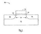
- FIG. 1A common configuration of such a transistor is shown in FIG. 1 . While the following discussion uses FIG. 1 to illustrate a transistor from the prior art, one skilled in the art will recognize that the present invention could be incorporated into the transistor shown in FIG. 1 to form a novel transistor according to the invention.
- the transistor 100is fabricated in a substrate 110 that is typically silicon, but could be fabricated from other semiconductor materials as well.
- the transistor 100has a source region 120 and a drain region 130 .
- a body region 132is located between source region 120 and drain region 130 , the body region 132 defining a channel of the transistor with a channel length 134 .
- a gate dielectric, or gate oxide 140is located on the body region 132 with a gate 150 located over the gate dielectric.
- the gate dielectriccan be formed from materials other than oxides, the gate dielectric is typically an oxide, and is commonly referred to as a gate oxide.
- the gatemay be fabricated from polycrystalline silicon (polysilicon) or other conducting materials such as metal may be used.
- the gate dielectric 140In fabricating transistors to be smaller in size and reliably operating on lower power supplies, one important design criteria is the gate dielectric 140 .
- the mainstay for forming the gate dielectrichas been silicon dioxide, SiO 2 .
- Thermally grown amorphous SiO 2provides an electrically and thermodynamically stable material, where the interface of a SiO 2 layer with an underlying Si provides a high quality interface as well as superior electrical isolation properties.
- use of SiO 2 on Sihas provided defect charge densities on the order of 10 10 /cm 2 , midgap interface state densities of approximately 10 10 /cm 2 eV, and breakdown voltages in the range of 15 MV/cm. With such qualities, there would be no apparent need to use a material other than SiO 2 , but with increased scaling, other requirements for gate dielectrics create the need to find other dielectric materials to be used for a gate dielectric.
- a method of forming a dielectric filmincludes evaporating a Ti source at a first rate to deposit Ti on a substrate, evaporating a lanthanide source at a second rate to deposit a lanthanide on the substrate, controlling the first rate and the second rate to form a lanthanide doped Ti film (a Ti/lanthanide film), and oxidizing the Ti/lanthanide film to grow a dielectric film on a substrate, where the dielectric film contains TiO x doped with the lanthanide.
- the lanthanideincludes evaporating a lanthanide selected from a group consisting of Nd, Tb, and Dy.
- the Ti and the lanthanideare evaporated using electron beam evaporation.
- the evaporation of Ti and lanthanideis assisted by ion beam bombardment of the substrate surface during deposition.
- the evaporation of the Ti and the lanthanideis followed by oxidation using a Kr/oxygen plasma.
- a gate dielectric formed as a dielectric film containing lanthanide doped TiO xhas a larger dielectric constant than silicon dioxide, a relatively small leakage current, and good stability with respect to a silicon based substrate.
- Embodiments according to the teachings of the present inventioninclude forming transistors, capacitors, memory devices, and electronic systems having dielectric layers containing lanthanide doped TiO x .
- Other embodimentsinclude structures for transistors, capacitors, memory devices, and electronic systems with gate dielectrics containing lanthanide doped TiO x .
- Such gate dielectricsprovide a significantly thinner equivalent oxide thickness compared with a silicon oxide gate having the same physical thickness.
- such gate dielectricsprovide a significantly thicker physical thickness than a silicon oxide gate dielectric having the same equivalent oxide thickness.
- FIG. 1shows a common configuration of a transistor in which an embodiment of a gate dielectric can be formed, according to the teachings of the present invention.
- FIG. 2illustrates an embodiment of an evaporation system for forming a film containing Ti doped with a lanthanide, according to the teachings of the present invention.
- FIG. 3illustrates an embodiment of a plasma oxidation system for forming a dielectric film containing lanthanide doped TiO x , according to the teachings of the present invention.
- FIG. 4illustrates a flow diagram of elements for an embodiment of a method for processing a dielectric film containing lanthanide doped TiO x , according to the teachings of the present invention.
- FIG. 5illustrates a flow diagram of elements for an embodiment of a method for processing a dielectric film containing lanthanide doped TiO x using electron beam evaporation followed by plasma oxidation, according to the teachings of the present invention.
- FIG. 6Ashows an embodiment of a layer of Ti doped with a lanthanide deposited on a substrate, according to the teachings of the present invention.
- FIG. 6Bshows an embodiment of a partially oxidized Ti layer doped with lanthanide on a substrate, according to the teachings of the present invention.
- FIG. 6Cshows an embodiment of a lanthanide doped TiO x film substantially completely oxidized and formed on a substrate, according to the teachings of the present invention.
- FIG. 7illustrates a flow diagram of elements for an embodiment of a computerized method for processing a dielectric film containing lanthanide doped TiO x , according to the teachings of the present invention.
- FIG. 8shows an embodiment of a configuration of a transistor capable of being fabricated according to the teachings of the present invention.
- FIG. 9shows an embodiment of a personal computer incorporating devices according to the teachings of the present invention.
- FIG. 10illustrates a schematic view of an embodiment of a central processing unit incorporating devices according to the teachings of the present invention.
- FIG. 11illustrates a schematic view of an embodiment of a DRAM memory device, according to the teachings of the present invention.
- wafer and substrate used in the following descriptioninclude any structure having an exposed surface with which to form the integrated circuit (IC) structure of the invention.
- substrateis understood to include semiconductor wafers.
- substrateis also used to refer to semiconductor structures during processing, and may include other layers that have been fabricated thereupon. Both wafer and substrate include doped and undoped semiconductors, epitaxial semiconductor layers supported by a base semiconductor or insulator, as well as other semiconductor structures well known to one skilled in the art.
- conductoris understood to include semiconductors, and the term insulator or dielectric is defined to include any material that is less electrically conductive than the materials referred to as conductors.
- horizontalas used in this application is defined as a plane parallel to the conventional plane or surface of a wafer or substrate, regardless of the orientation of the wafer or substrate.
- verticalrefers to a direction perpendicular to the horizontal as defined above. Prepositions, such as “on”, “side” (as in “sidewall”), “higher”, “lower”, “over” and “under” are defined with respect to the conventional plane or surface being on the top surface of the wafer or substrate, regardless of the orientation of the wafer or substrate.
- a gate dielectric 140 of FIG. 1when operating in a transistor, has both a physical gate dielectric thickness and an equivalent oxide thickness (t eq ).
- the equivalent oxide thicknessquantifies the electrical properties, such as capacitance, of a gate dielectric 140 in terms of a representative physical thickness.
- t eqis defined as the thickness of a theoretical SiO 2 layer that would be required to have the same capacitance density as a given dielectric, ignoring leakage current and reliability considerations.
- a SiO 2 layer of thickness, t, deposited on a Si surface as a gate dielectricwill have a t eq larger than its thickness, t.
- This t eqresults from the capacitance in the surface channel on which the SiO 2 is deposited due to the formation of a depletion/inversion region.
- This depletion/inversion regioncan result in t eq being from 3 to 6 Angstroms ( ⁇ ) larger than the SiO 2 thickness, t.
- the gate dielectric equivalent oxide thicknessto under 10 ⁇
- the physical thickness requirement for a SiO 2 layer used for a gate dielectricwould be need to be approximately 4 to 7 ⁇ .
- SiO 2 layerAdditional requirements on a SiO 2 layer would depend on the gate electrode used in conjunction with the SiO 2 gate dielectric. Using a conventional polysilicon gate would result in an additional increase in t eq for the SiO 2 layer. This additional thickness could be eliminated by using a metal gate electrode, though metal gates are not currently used in complementary metal-oxide-semiconductor field effect transistor (CMOS) technology. Thus, future devices would be designed towards a physical SiO 2 gate dielectric layer of about 5 ⁇ or less. Such a small thickness requirement for a SiO 2 oxide layer creates additional problems.
- CMOScomplementary metal-oxide-semiconductor field effect transistor
- Silicon dioxideis used as a gate dielectric, in part, due to its electrical isolation properties in a SiO 2 —Si based structure. This electrical isolation is due to the relatively large band gap of SiO 2 (8.9 eV) making it a good insulator from electrical conduction. Signification reductions in its band gap would eliminate it as a material for a gate dielectric. As the thickness of a SiO 2 layer decreases, the number of atomic layers, or monolayers of the material in the thickness decreases. At a certain thickness, the number of monolayers will be sufficiently small that the SiO 2 layer will not have a complete arrangement of atoms as in a larger or bulk layer.
- a thin SiO 2 layer of only one or two monolayerswill not form a full band gap.
- the lack of a full band gap in a SiO 2 gate dielectricwould cause an effective short between an underlying Si channel and an overlying polysilicon gate.
- This undesirable propertysets a limit on the physical thickness to which a SiO 2 layer can be scaled.
- the minimum thickness due to this monolayer effectis thought to be about 7-8 ⁇ . Therefore, for future devices to have a t eq less than about 10 ⁇ , other dielectrics than SiO 2 need to be considered for use as a gate dielectric.
- materials with a dielectric constant greater than that of SiO 2 , 3.9will have a physical thickness that can be considerably larger than a desired t eq , while providing the desired equivalent oxide thickness.
- an alternate dielectric material with a dielectric constant of 10could have a thickness of about 25.6 ⁇ to provide a t eq of 10 ⁇ , not including any depletion/inversion layer effects.
- the reduced equivalent oxide thickness of transistorscan be realized by using dielectric materials with higher dielectric constants than SiO 2 .
- the thinner equivalent oxide thickness required for lower transistor operating voltages and smaller transistor dimensionsmay be realized by a significant number of materials, but additional fabricating requirements makes determining a suitable replacement for SiO 2 difficult.
- the current view for the microelectronics industryis still for Si based devices. This requires that the gate dielectric employed be grown on a silicon substrate or silicon layer, which places significant restraints on the substitute dielectric material. During the formation of the dielectric on the silicon layer, there exists the possibility that a small layer of SiO 2 could be formed in addition to the desired dielectric. The result would effectively be a dielectric layer consisting of two sublayers in parallel with each other and the silicon layer on which the dielectric is formed. In such a case, the resulting capacitance would be that of two dielectrics in series.
- the t eqis again limited by a SiO 2 layer.
- the t eqwould be limited by the layer with the lowest dielectric constant.
- the layer interfacing with the silicon layermust provide a high quality interface to maintain a high channel carrier mobility.
- Dielectric Constant Band gap Material( ⁇ ) E g (eV) Crystal Structure(s) SiO 2 3.9 8.9 Amorphous Si 3 N 4 7 5.1 Amorphous Al 2 O 3 9 8.7 Amorphous Y 2 O 3 15 5.6 Cubic La 2 O 3 30 4.3 Hexagonal, Cubic Ta 2 O 3 26 4.5 Orthorhombic TiO 2 80 3.5 Tetrag. (rutile, anatase) HfO 2 25 5.7 Mono., Tetrag., Cubic ZrO 2 25 7.8 Mono., Tetrag., Cubic
- SiO 2as a gate dielectric
- the formation of the SiO 2 layer resultsis an amorphous gate dielectric.
- Having an amorphous structure for a gate dielectricavoids high leakage paths associated with grain boundaries in polycrystalline gate dielectrics. Additionally, grain size and orientation changes throughout a polycrystalline gate dielectric can cause variations in the film's dielectric constant.
- the materials having the advantage of a high dielectric constants relative to SiO 2also have the disadvantage of a crystalline form, at least in a bulk configuration.
- the best candidates for replacing SiO 2 as a gate dielectricare those with high dielectric constant, which can be fabricated as a thin layer with an amorphous form.
- TiO 2Based solely on the size of the dielectric constant, titanium oxide, TiO 2 , appears to be an excellent candidate for replacing SiO 2 . However, TiO 2 does not provide the electrical properties generally desired for integrated circuits, such as, high electric field breakdown and low leakage current. Dielectric films substituting various cations into amorphous TiO x films by magnetron sputtering were found to provide improved electric field breakdown and leakage current with respect to undoped TiO 2 films. See, R. B. Dover, Applied Physics Letters , vol. 74: no. 20, pp. 3041-3043 (2001).
- particles of the material to be depositedbombard the surface at a high energy. When a particle hits the surface, some particles adhere, and other particles cause damage. High energy impacts remove body region particles creating pits.
- the surface of such a deposited layercan have a rough contour due to the rough interface at the body region.
- An embodiment of the teachings of the present inventionincludes dielectric films containing TiO x doped with a lanthanide formed by ion assisted electron beam evaporation followed by plasma oxidation.
- Dielectric films formed on a substrate in such a mannerwill have a surface that is smoother than a film formed in another fashion such as sputtering. This increased smoothness, or decreased roughness, is due in part to the use of high purity target materials for evaporation.
- additional energyis provided for activation at the deposition interface to provide for increased packing density of the dielectric film.
- the dielectric filmis not only smoother, but is more durable in a humid environment.
- oxidation in a microwave-excited plasma system using a radial line slotted antennaprovides for the formation of a uniform oxide layer.
- FIG. 2illustrates an embodiment of an evaporation system 200 for forming a film containing Ti doped with a lanthanide, according to the teachings of the present invention.
- Evaporation system 200includes a reaction chamber 205 in which is located a substrate 210 having a surface 212 that is to be processed. Substrate 210 rests on substrate holder 215 and its temperature can be raised above room temperature using a heater 220 with its associated reflector 225 .
- Evaporation system 200also includes a first electron gun device 230 regulated by electron gun controller 232 and a second electron gun device 235 regulated by electron gun controller 237 for depositing material on substrate surface 212 .
- an ion gun 240is provided in evaporation system 200 .
- Ionizer ring 245provides supplemental oxygen for processes that require additional oxygen due to lost of oxygen in the evaporation of target materials. For target materials substantially void of oxygen, ionizer ring 245 provides initial oxygen to a film deposited on substrate surface 212 that is to undergo a subsequent oxidation process.
- Shutter 250is used in conjunction with the control of electron gun devices 230 , 235 to control the growth rate of a film on substrate 210 . The growth rate is determined using quartz crystal monitors 255 , 260 . The quartz crystal monitors 255 , 260 are coupled to a thickness/rate control 265 , typically located outside reaction chamber 205 .
- ozone gas source 270including a mass-flow controller 275 , and an ion gas source 280 .
- Mass-flow controller 275controls the flow of ozone into reaction chamber 205 .
- Gas for the ion gun 240is controlled by an ion gun controller 285 including a mass-flow controller 290 .
- a vacuum pump 295 with mass flow controller 298maintains the overall atmosphere of evaporation system 200 at desired levels prior to, during, and after evaporation.
- Electron gun device 230can include an electron gun and receptacle for a target material that is to be evaporated.
- Target material placed in the target receptacle of electron gun device 230is heated by impact from an electron beam from its associated electron gun.
- the electron beamis generated with an intensity and duration with which to evaporate the material in the target receptacle of electron gun device 230 .
- the evaporated materialthen distributes throughout the reaction chamber 205 .
- the evaporated material and pre-evaporation contaminantsare prevented from depositing on substrate surface 212 in an unwanted manner by shutter 250 .
- Electron gun device 235is similar to electron gun device 235 . In one embodiment, these devices can incorporate multiple target receptacles. Further, electron gun devices 230 , 235 can be realized using commercially available devices as are known to those skilled in the art.
- Ion gun 240is a typical ion gun as is known in the art. In one embodiment, ion gun 240 provides an ion beam with an incident angle that is within +40° to ⁇ 40° relative to the substrate surface 212 . In one embodiment, ion gun 240 is a filament-type ion gun with a relatively large diameter ranging from 7.6 cm to 10 cm, which uses a hot filament to ionize gas from gas source 280 . Alternately, a cold catheter discharge gun can be used. Commercial ion guns are available as is known to those skilled in the art. Ion gun 240 regulated by ion gun controller 285 provides ions that are directed at the substrate surface 212 .
- the impact of the ionsprovides activation energy for the formation of a dielectric film as evaporated material interacts with substrate surface 212 .
- the ionsalso pass through ionizer ring 245 as they travel to substrate surface 212 .
- Ionizer ring 245provides oxygen necessary to compensate for loss of oxygen in the evaporated target material, or to add initial oxygen for subsequent oxidation processing.
- itincludes a ring with a center axis.
- the ringhas a plurality of openings adapted to direct ozone flowing to ionizer ring 245 from ozone gas source 270 towards substrate surface 212 .
- Ozoneis uniformly distributed to substrate surface 212 by ionizer ring 245 positioned generally parallel to substrate 210 .
- ionizer ring 245has a size that does not inhibit the ion beam directed at substrate surface 212 .
- Evaporation system 200can be used to evaporate oxide material or non-oxygen material.
- evaporation system 200is used in conjunction with another system for oxidizing a metallic film formed on a substrate in evaporation system 200 .
- Such a oxidation system that can be used following processing in evaporation system 200is a plasma oxidation system.
- FIG. 3illustrates an embodiment of a plasma oxidation system 300 for forming a dielectric film containing lanthanide doped TiO x , according to the teachings of the present invention.
- Plasma oxidation system 300includes a reaction chamber 305 in which is located a substrate 310 having a surface 312 that is to be processed. Substrate 310 rests on substrate holder 315 and its temperature can be raised above room temperature using a heater 320 .
- Plasma oxidation system 300also includes a microwave generator 325 , a co-axial waveguide 330 , a radial line slot antenna 335 , and a microwave radiation plate 340 for generating a microwave excited plasma.
- plasma oxidation system 300To focus on the use of plasma oxidation system 300 in the various embodiments of the present invention, detailed elements of the plasma oxidation system are not shown. For example, gas inlets, vacuum ports, and various control apparatus, as are known to those skilled in the art, are not shown.
- Plasma oxidation system 300provides circularly polarized microwaves that emanate from radial line slot antenna 335 , having been generated by microwave generator 325 and transmitted through co-axial waveguide 330 .
- the microwavesinteract with gases to produce a plasma.
- An oxidation process using this systememploys a mixture of oxygen an inert gases.
- the gas mixturecan include an oxygen concentration from about 2% to about 4% by volume of the gas mixture.
- Suitable inert gasescan include krypton and helium.
- Microwave interactionis effective to form atomic oxygen that can readily interact with the surface 312 of a substrate 310 .
- use of a radial line slot antennagives rise to superior uniformity of the oxide across substrate surface 312 as well as high plasma density and low electron temperature.
- a plasma oxidation systemis described in co-pending, commonly assigned U.S. patent application: entitled “Methods for Forming Dielectric Materials and Methods for Forming Semiconductor Devices,” attorney docket no. MI122-1530, Ser. No. 09/908,767, which is incorporated herein by reference.
- the use, construction and fundamental operation of a plasma oxidation system for forming oxide filmsare understood by those of ordinary skill in the art of semiconductor fabrication.
- the embodiments of the present inventioncan be practiced on a variety of such plasma oxidation systems without undue experimentation.
- one of ordinary skill in the artwill comprehend the necessary detection, measurement, and control techniques in the art of semiconductor fabrication upon reading the disclosure.
- evaporation system 200 and plasma oxidation system 300can be controlled by a computer.
- the computeris not shown.
- the individual elementssuch as pressure control, temperature control, deposition rate control, electron gun operation, ion gun operation, and microwave generation within evaporation system 200 /plasma oxidation system 300 can be under computer control.
- instructions stored in a computer readable mediumare executed by a computer to accurately control the integrated functioning of the elements of evaporation system 200 /plasma oxidation system 300 to form a dielectric film containing TiO x doped with a lanthanide.
- FIG. 4illustrates a flow diagram of elements for an embodiment of a method for processing a dielectric film containing lanthanide doped TiO x , according to the teachings of the present invention.
- a method of forming a dielectric filmincludes evaporating a Ti source at a first rate to deposit Ti on a substrate, at block 405 , evaporating a lanthanide source at a second rate to deposit lanthanide on the substrate, at block 410 , and oxidizing the deposited Ti and lanthanide using atomic oxygen generated in a plasma, at block 415 .
- the lanthanideis selected from a group consisting of Nd, Tb, and Dy.
- Tiis evaporated by electron beam evaporation.
- the lanthanidecan also be evaporated using electron beam evaporation.
- the Ti and/or the lanthanidecan be evaporated by other processes including thermal evaporation.
- the substrate surfaceis bombarded with ions to facilitate the deposition of the Ti and the lanthanide.
- Argon ionscan be used in the ion bombardment, or alternately xenon ions.
- the Ti and the lanthanidecan be evaporated at substantially the same time with different rates of evaporation to insure that a film formed on a substrate surface has lanthanide dispersed throughout the film prior to oxidizing with a plasma.
- oxidizing with a plasmacan be accomplished with atomic oxygen generated in a Krypton/oxygen plasma.
- the plasmacan be generated using helium.
- oxygenis supplied during the evaporation of the Ti and the lanthanide to provide a small seed amount of oxygen into the film prior to oxidation.
- This initial supply of oxygenis provided using an ionizer ring.
- the ionizer ringis effectively turned off to provide a substantially oxygen free film for plasma oxidation.
- the first rate for evaporating Ti and the second rate for evaporating lanthanideis controlled to provide a film containing Ti doped with a predetermined percentage of the lanthanide.
- the Ti filmcan be doped in the range from about 10% to about 30% of lanthanide.
- oxidizing the Ti/lanthanide filmproduces a dielectric film doped in the range from about 5% to about 40% of lanthanide.
- controlling the first and second rateallows the dielectric film to be formed having a dielectric constant ranging from about 50 to about 110.
- FIG. 5illustrates a flow diagram of elements for an embodiment of a method for processing a dielectric film containing lanthanide doped TiO x using electron beam evaporation followed by plasma oxidation, according to the teachings of the present invention.
- a method of forming a dielectric filmincludes evaporating a Ti source at a first rate using a first electron gun, at block 505 , evaporating a lanthanide source at a second rate using a second electron gun, at block 510 , controlling the first rate and the second rate to deposit a film on a substrate, the film containing Ti doped with the lanthanide, at block 515 , and oxidizing the film material using atomic oxygen generated in a plasma, at block 520 .
- An embodiment of this methodcan be realized using evaporation system 200 of FIG. 2 and plasma oxidation system 300 of FIG. 3 .
- An embodiment of a formation of a lanthanide doped TiO x dielectric filmincludes forming such a film as a gate dielectric of a transistor.
- Evaporation system 200is prepared by locating a substrate 210 on substrate holder 215 .
- Substrate 210is a material used for forming a transistor such as a silicon or silicon containing material. In other embodiments, germanium, gallium arsenide, silicon-on-sapphire substrates, or other suitable substrates may be used. This preparation process includes cleaning of the substrate 210 and forming layers and regions of the substrate, such as drains and sources of a metal oxide semiconductor (MOS) transistor, prior to forming a gate dielectric.
- MOSmetal oxide semiconductor
- the sequencing of the formation of the regions of the transistor being processedfollows typical sequencing that is generally performed in the fabrication of a MOS transistor as is well known to those skilled in the art. Included in the processing prior to forming a gate dielectric is the masking of substrate regions to be protected during the gate dielectric formation, as is typically performed in MOS fabrication. In this embodiment, the unmasked region includes a body region of a transistor, however one skilled in the art will recognize that other semiconductor device structures may utilize this process. Additionally, the substrate 210 in its ready for processing form is conveyed into a position in reaction chamber 205 to undergo an ion assisted electron beam evaporation process.
- Evaporation system 200is also prepared by loading a Ti target, or Ti source, into electron gun device 230 and loading a lanthanide target, or lanthanide source, into electron gun device 235 .
- the lanthanideis used to provide a dopant for a TiO x film to be grown on substrate surface 212 .
- the lanthanidecan be selected from a group consisting of Nd, Tb, and Dy.
- the Ti sourcecan include Ti slugs, where the Ti slugs are at least 99.9999% pure.
- the lanthanide sourcecan include a lanthanide that is at least 99.999% pure.
- the lanthanide dopant source materialcan be in the form of a powder. In other embodiments, other materials of varying degrees of purity can be used as a dopant in an amorphous TiO x film. Additionally, a Ti source of less purity can also be used in an embodiment.
- Reaction chamber 205is evacuated to a low pressure to maintain the substrate surface clean and in condition for processing.
- reaction chamberis brought to and maintained at a pressure of about 2 ⁇ 10 ⁇ 7 Torr prior to evaporating the Ti target and evaporating the lanthanide target. While, in one embodiment, during the evaporation process, reaction chamber 205 is maintained at a pressure of about 2 ⁇ 10 ⁇ 6 Torr during deposition.
- the pressure in reaction chamber 205is controlled by vacuum pump 295 through mass-flow controller 298 .
- the environment of reaction chamber 205is further prepared by raising the temperature of substrate 210 using heater 220 and its associated reflector 225 .
- the substrate temperatureis raised to and maintained at a temperature ranging from about 100° C. to about 200° C. prior to and during the formation of the film containing Ti and the lanthanide.
- Electron gun device 230regulated by electron gun controller 232 , evaporates Ti into reaction chamber 205 where it is distributed throughout.
- the selected lanthanideis evaporated using electron gun device 235 regulated by electron gun controller 237 , co-mingling the evaporated lanthanide with the evaporated Ti.
- the evaporated materialis deposited on substrate surface 212 .
- the rates for forming the layer of Ti and lanthanide grown on substrate surface 212is regulated using thickness/rate control 265 that receives growth information from quartz crystal monitors 255 , 260 .
- the Ti evaporation and the lanthanidecan be performed with one electron gun device having multiple target receptacles that can be shielded from each other.
- the electron gun devicecan further include either two electron guns individually controlled or one electron gun whose electron beam can be multiply controlled providing two beams directed individually in two directions. In such cases, the electron gun device acts as two electron guns, where one generated beam defines a first electron gun and a second generated beam defines a second electron gun.
- oxygencan be supplied at the substrate surface 212 by ionizer ring 245 .
- Ozoneis supplied from ozone gas source 270 with flow controlled by mass-flow controller 275 through the openings in ionizer ring 245 .
- the partial pressure of ozone in reaction chamber 205is in the range of about 2 ⁇ 10 ⁇ 5 torr to about 8 ⁇ 10 ⁇ 5 torr. Parameters for ozone partial pressure can be determined from measuring oxygen content in the deposited film using the quartz crystal monitors 255 , 260 .
- the oxygencan be supplied to provide an initial amount of oxygen dispersed throughout the lanthanide doped Ti film (the Ti/lanthanide film) to assist subsequent plasma oxidation.
- the ozone flowcan be maintained in an off state to provide a Ti/lanthanide film that is substantially oxygen free prior to plasma oxidation.
- Evaporation of the Ti and the lanthanide including supplementing with oxygenprovides the initial start material for forming an amorphous TiO x dielectric layer doped with the lanthanide.
- substrate surfaceis bombarded with argon ions. The ion bombardment is initiated shortly after beginning the evaporation process so that at least an initial monolayer or so of Ti doped with the lanthanide is formed.
- an argon beamis directed at substrate surface 212 at about one to two seconds after the evaporation process is initiated.
- Ion gun controller 285regulates the flow of argon gas through mass-flow controller 290 providing an argon beam density in the range of about 0.5 ma/cm 2 to about 1 ma/cm 2 .
- inert gases used in the ion beam processcan include xenon and krypton at various beam densities.
- Use of the electron gun controllers 232 , 237 in conjunction with thickness/rate control 265allows the Ti to be evaporated at a first rate, and the lanthanide to be evaporated at a second rate.
- a lanthanide doped Ti filmcan be formed on substrate surface 212 with the Ti film doped in the range from about 10% to about 30% of the lanthanide. Controlling the evaporation rates allows the lanthanide to be selectively doped in the Ti film within a predetermined range for the percentage of the lanthanide in the film.
- Further processing to form an oxideresults in a dielectric film of TiO x doped with the lanthanide, where the dielectric film can be selectively grown, doped in the range from about 5% to about 40% of the lanthanide.
- controlling the first rate and the second rateprovides for growing on substrate 210 an amorphous TiO x film doped with a lanthanide, where the dielectric film has a dielectric constant ranging from about 50 to about 110.
- the first evaporation ratecan also be controlled such that the Ti can be evaporated at a rate ranging from about 0.2 nm/sec to about 0.5 nm/sec.
- the second ratecan be controlled such that the lanthanide is evaporated at a rate ranging from about 0.2 nm/sec to about 0.5 nm/sec.
- the plasma oxidation system 300 of FIG. 3can be included as part of an overall processing system including evaporation system 200 of FIG. 2 .
- plasma oxidation system 300can be connected to evaporation system 200 using sealable connections to maintain the substrate, which is substrate 210 in FIG. 2 and substrate 310 of FIG. 3 , in an appropriate environment between Ti/lanthanide evaporation processing and plasma oxidation.
- Other meansas are known to those skilled in the art can be employed for maintaining an appropriate environment between different processing procedures.
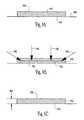
- FIGS. 6A-6Cshow a low temperature plasma oxidation process using plasma oxidation system 300 of FIG. 3 in one embodiment to form a layer of lanthanide doped TiO x .
- FIG. 6Ashows an embodiment of a Ti/lanthanide layer 610 deposited on a substrate 600 having an substrate interface 620 , according to the teachings of the present invention.
- Ti/lanthanide layer 610is deposited on substrate 600 by electron beam evaporation, as discussed above, providing a film with an outer surface 630 .
- Layer 610is deposited over a body region of a transistor, however the layers may be deposited on any surface within the scope of the invention.
- FIG. 6Bshows an embodiment of a partially oxidized Ti/lanthanide layer 650 on substrate 600 , according to the teachings of the present invention.
- the Ti/lanthanide layer 610is in the process of being oxidized.
- the oxidation processincludes a krypton/oxygen mixed plasma oxidation process.
- the mixed plasma processgenerates atomic oxygen or oxygen radicals in contrast to molecular oxygen or O 2 used in conventional thermal oxidation.
- the atomic oxygenis introduced to the layer from all exposed directions as indicated by arrows 640 , creating an oxide portion 650 .
- the atomic oxygencontinues to react with the layer and creates an oxidation interface 622 . As the reaction progresses, atomic oxygen diffuses through the oxide portion 650 and reacts at the oxidation interface 622 until the layer is completely converted to an oxide of the deposited material layer.
- FIG. 6Cshows an embodiment of a lanthanide doped TiO x substantially completely oxidized and formed on substrate 600 , according to the teachings of the present invention.
- FIG. 6Cshows the resulting oxide layer 650 which spans a physical thickness 652 from the outer surface 630 to the interface 620 .
- the overall thickness 652 of the lanthanide doped TiO x layer in FIG. 6Chas increased from that of the Ti/lanthanide layer deposited on substrate 600 in FIG. 6A , due to the oxidation of the Ti/lanthanide layer.
- the processing variables for the mixed plasma oxidationinclude a low ion bombardment energy of less than about 7 eV, a high plasma density above 10 12 /cm 3 and a low electron temperature below about 1.3 eV.
- the substrate temperatureis maintained at about 400° C.
- a mixed gas consisting of krypton and oxygen with the oxygen content at 3%is used at a pressure of about 1 Torr.
- microwaves having a frequency of about 8.3 GHZ and a power density of about 4 W/cm 2are used.
- the oxidation processcan provide a growth rate of about 1.5 nm/min.
- the low temperature mixed plasma oxidation process described aboveallows the deposited layer to be oxidized at a low temperature.
- the mixed plasma processin one embodiment is performed at approximately 400° C. in contrast to prior thermal oxidation processes that are performed at approximately 1000° C.
- a dielectric film of TiO x doped with the lanthanidecan be selectively grown with lanthanide doping in the range from about 5% to about 40% of the lanthanide. Further, controlling the first rate and the second rate of evaporation followed by oxidation by a Kr/oxygen plasma provides for growing on substrate 210 an amorphous TiO x film doped with a lanthanide, where the dielectric film has a dielectric constant ranging from about 50 to about 110.
- a method for forming a lanthanide doped TiO x dielectric filmincludes evaporating a Ti source at a first rate using a first electron gun, evaporating a lanthanide source at a second rate using a second electron gun, controlling the first rate and the second rate to deposit a film on a substrate, bombarding a surface of the substrate with ions during evaporation of the Ti and the lanthanide, and oxidizing the film using atomic oxygen generated in a plasma, wherein the dielectric film contains lanthanide doped TiO x .
- the lanthanidecan be selected from a group consisting of Nd, Tb, and Dy.
- the dielectric filmis grown with a predetermined percentage of lanthanide doping.
- bombarding substrate surface 212 with ions during the Ti evaporation and/or the lanthanide evaporationincludes bombarding substrate surface 212 during any part of the Ti and the lanthanide evaporation process.
- a method for forming a lanthanide doped TiO x dielectric filmincludes evaporating a Ti source at a first rate using a first electron gun, evaporating a lanthanide source at a second rate using a second electron gun, controlling the first rate and the second rate to deposit a film on a substrate, supplementing with oxygen using an ionizer ring during the deposition of the Ti and the lanthanide, and oxidizing the film using atomic oxygen generated in a plasma, where the dielectric film contains lanthanide doped TiO x .
- the lanthanidecan be selected from a group consisting of Nd, Tb, and Dy.
- the dielectric filmis grown with a predetermined percentage of lanthanide doping.
- the lanthanide doped TiO x dielectric layer grown according to these various embodimentswill provide smoother surfaces than expected from other current methods, which translates to higher breakdown electric fields and lower leakage currents. Additionally, the oxide formation across the substrate is more uniform than with other methods.
- FIG. 7illustrates a flow diagram of elements for an embodiment of a computerized method to process a dielectric film containing lanthanide doped TiO x , according to the teachings of the present invention.
- a computerized method of forming a dielectric filmincludes controlling an environment of a reaction chamber, at block 705 , controlling evaporation of a Ti source in the reaction chamber at a first rate, at block 710 , controlling evaporation of a lanthanide source in the reaction chamber at a second rate, at block 715 , controlling the first rate and the second rate to deposit a film on a substrate, where the film contains Ti doped with the lanthanide, at block 720 , and controlling oxidation of the film using atomic oxygen generated in a plasma to form a dielectric film containing TiO x doped with the lanthanide, at block 725 .
- Controlling the evaporation ratesallows the lanthanide to be selectively doped into the Ti film within a predetermined range for the percentage of the lanthanide in the film.
- An embodiment of this methodcan be realized using evaporation system 200 of FIG. 2 and plasma oxidation system 300 of FIG. 3 , where the controls for the individual elements of evaporation system 200 and the individual elements of plasma oxidation system 300 are coupled to a computer, not shown in FIG. 200 or FIG. 300 .
- the computerprovides control of the Ti evaporation by regulating the operation of electron gun device 230 by controlling electron gun control 232 .
- the computerprovides control of the lanthanide evaporation by regulating the operation of electron gun device 235 by controlling electron gun control 237 .
- the computercan control ion gun controller 285 and mass-flow controller 290 to regulate the ion beam generated by ion gun 240 .
- the computercan regulate supplementing oxygen at substrate surface 212 by regulating the amount of ozone directed to ionizer 245 by controlling the mass-flow controller 275 .
- the computercan also control the environment of reactor chamber 205 in which a film is being formed on substrate 210 .
- the computerregulates the pressure in reaction chamber 205 within a predetermined pressure range by controlling vacuum pump 295 and mass-flow controller 298 .
- the computeralso regulates the temperature range for substrate 210 within a predetermined range by controlling heater 220 . Further, the computer controls unwanted material from reaching the substrate surface 212 by controlling shutter 250 .
- the computercontrols a first rate for Ti evaporation and a second rate for lanthanide evaporation to selectively grow a Ti film doped in the range from about 10% to about 30% of the lanthanide. Further, the computer can control the first rate and the second rate such that subsequent oxidation results in the growth of an amorphous TiO x film doped with a lanthanide in the range of about 5% to about 40% of the lanthanide, where the TiO x film has a dielectric constant ranging from about 50 to about 110.
- the computercan also control the elements of evaporation system 200 to achieve the operating parameters as previously discussed in the embodiments for forming a Ti/lanthanide film.
- the substrate 210 of FIG. 2becomes substrate 310 to be oxidized in the microwave excited plasma oxidation system 300 of FIG. 3 .
- the elements of plasma oxidation system 300are controlled by the computer that controls evaporation system 200 .
- plasma oxidation system 300can be controlled by a separate computer.
- the computercontrols microwave generator 325 that supplies the microwaves in reaction chamber 305 . It also regulates heater 320 to control the temperature of substrate 310 . Though the gas inlets and vacuum ports with their associated mass-flow controllers are not shown in FIG. 3 , these elements are regulated by the computer to control the plasma parameters and pressure in reaction chamber 305 .
- FIGS. 2 and 3For convenience, the individual control lines to elements of evaporation system 200 , and plasma oxidation system 300 , as well as a computer, are not shown in FIGS. 2 and 3 .
- the above descriptions of the computer control in conjunction with FIGS. 2 , 3provide information for those skilled in the art to practice embodiments for forming a dielectric layer containing lanthanide doped TiO x using a computerized method as described herein.
- a computer for controlling the elements of evaporation system 200 of FIG. 2 and plasma oxidation system 300 of FIG. 3operates under computer-executable instructions to perform a method for forming a dielectric film that can include controlling an environment of a reaction chamber, controlling evaporation of a Ti source in the reaction chamber at a first rate, controlling evaporation of a lanthanide source in the reaction chamber at a second rate, controlling the first rate and the second rate to deposit a film on a substrate, where the film contains Ti doped with the lanthanide, and controlling oxidation of the film using atomic oxygen generated in a plasma to form a dielectric film containing lanthanide doped TiO x .
- Controlling the evaporation ratesallows the lanthanide to be selectively doped into the Ti film within a predetermined range for the percentage of the lanthanide in the film.
- Using a computer to control parameters for growing the dielectric filmprovides for processing the dielectric film over a wide range of parameters allowing for the determination of an optimum parameter set for the evaporation system/plasma oxidation system used.
- the computer-executable instructionscan be provided in any computer-readable medium. Such computer-readable medium includes, but is not limited to, floppy disks, diskettes, hard disks, CD-ROMS, flash ROMS, nonvolatile ROM, and RAM.
- t equseful equivalent oxide thickness
- the relatively large dielectric constant for material layers of lanthanide doped TiO xallows for the engineering of dielectric films having a physical thickness in the 100 nm (1000 ⁇ ) range, while achieving a t eq of less than 100 ⁇ . Further, growing ultra-thin layers, or films, of lanthanide doped TiO x provides for t eq in the range of several monolayers. From above, it is apparent that a film containing lanthanide doped TiO x can be attained with a t eq ranging from 1.5 ⁇ to 5 ⁇ . Further, such a film can provide a t eq significantly less than 2 or 3 ⁇ , even less than 1.5 ⁇ .
- dielectric films of lanthanide doped TiO x formed by ion assisted electron beam evaporation followed plasma oxidationcan provide not only ultra thin t eq films, but also films with relatively low leakage current.
- attainment of relatively low leakage currentis engineered by doping with lanthanides selected from a group consisting of Nd, Tb, and Dy.
- lanthanidesselected from a group consisting of Nd, Tb, and Dy.
- a layer of undoped TiO xis typically amorphous, which assists the reduction of leakage current, evaporating these lanthanides during the evaporation of the Ti layer provides a layer for oxidation that subsequently yields a doped amorphous TiO x with enhanced leakage current characteristics.
- Leakage currents on the order of 10 ⁇ 7 A/cm 2 or smaller in TiO x layers doped with Nd, Tb, or Dycan be attained, which are orders of magnitude smaller than for undoped TiO x .
- the breakdown electric fieldsare several factors larger for layers of TiO x doped with Nd, Tb, or Dy than for layers of undoped TiO x .
- the doping of the TiO x layer with a lanthanideoccurs as a substitution of a lanthanide atom for a Ti atom.
- the resultant doped TiO x layeris a layer of amorphous Ti 1 ⁇ y L y O x , where L is a lanthanide. Controlling the evaporation of Ti, the evaporation of the selected lanthanide, and the plasma oxidation allows a Ti 1 ⁇ y L y O x , or lanthanide doped TiO x , dielectric layer to be formed where the lanthanide, L, can range from about 5% to about 40% of the dielectric layer formed.
- Such TiO x layers doped with Nd, Tb, or Dy formed by ion bean assisted electron beam evaporation followed by plasma oxidationcan provide the reduced leakage current and increased breakdown electric fields mentioned above.
- a transistor 100 as depicted in FIG. 1can be formed by forming a source region 120 and a drain region 130 in a silicon based substrate 110 where the source region 120 and the drain region 130 are separated by a body region 132 .
- the body region 132 separated by the source 120 and the drain 130defines a channel having a channel length 134 .
- Tiis evaporated using an electron gun at a controlled rate.
- a lanthanide selected from a group consisting of Nd, Tb, and Dyis evaporated using a second electron gun at a second controlled rate.
- Evaporating the lanthanide sourceis begun substantially concurrent with evaporating Ti, forming a film 140 containing Ti and lanthanide on the body region, while the body region is bombarded with Ar ions shortly after the deposition of Ti on the body region has begun.
- Film 140or layer 140 , is oxidized using a Kr/oxygen plasma.
- a gateis formed over the gate dielectric 140 .
- forming the gateincludes forming a polysilicon layer, though a metal gate can be formed in an alternative process.
- Forming the substrate, source region, drain region, and the gateis performed using standard processes known to those skilled in the art. Additionally, the sequencing of the various elements of the process for forming a transistor is conducted with standard fabrication processes, also as known to those skilled in the art.
- FIG. 8shows an embodiment of a configuration of a transistor 800 capable of being fabricated, according to the teachings of the present invention.
- transistor 800includes a silicon based substrate 810 with a source 820 and a drain 830 separated by a body region 832 .
- the body region 832 between the source 820 and the drain 830defines a channel region having a channel length 834 .
- a stack 855including a gate dielectric 840 , a floating gate 852 , a floating gate dielectric 842 , and control gate 850 .
- the gate dielectric 840can be formed as described above with the remaining elements of the transistor 800 formed using processes known to those skilled in the art. Alternately, both the gate dielectric 840 and the floating gate dielectric 842 can be formed as dielectric layers containing lanthanide doped TiO x in various embodiments as described herein.
- a methodcan include forming a first conductive layer, evaporating a Ti source at a first rate, evaporating a lanthanide source at a second rate, controlling the first rate and the second rate to form a Ti/lanthanide film on the first conductive layer, oxidizing the Ti/lanthanide film using a plasma to form a dielectric film, and forming a second conductive layer on the dielectric.
- a capacitorcan be formed by forming a conductive layer on a substrate, forming a dielectric film containing lanthanide doped TiO x using any of the embodiments described herein, and forming another conductive layer on the dielectric film.
- Transistors, capacitors, and other devices having dielectric films or layers created by the methods described abovemay be implemented into memory devices and electronic systems including information handling devices.
- Information handling devices having a dielectric layer containing lanthanide doped TiO xcan be constructed using various embodiments of the methods described above. Such information devices can include wireless systems, telecommunication systems, and computers.
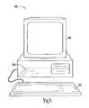
- An embodiment of a computer having a dielectric layer containing lanthanide doped TiO xis shown in FIGS. 9-11 and described below. While specific types of memory devices and computing devices are shown below, it will be recognized by one skilled in the art that several types of memory devices and electronic systems including information handling devices utilize the invention.
- a personal computercan include a monitor 900 , keyboard input 902 and a central processing unit 904 .
- the processor unittypically includes microprocessor 1006 , memory bus circuit 1008 having a plurality of memory slots 1012 ( a-n ), and other peripheral circuitry 1010 .
- Peripheral circuitry 1010permits various peripheral devices 1024 to interface processor-memory bus 1020 over input/output (I/O) bus 1022 .
- the personal computer shown in FIGS. 9 and 10also includes at least one transistor having a gate dielectric in accordance with an embodiment of the present invention.
- Microprocessor 1006produces control and address signals to control the exchange of data between memory bus circuit 1008 and microprocessor 1006 and between memory bus circuit 1008 and peripheral circuitry 1010 . This exchange of data is accomplished over high speed memory bus 1020 and over high speed I/O bus 1022 .
- Coupled to memory bus 1020are a plurality of memory slots 1012 ( a-n ) which receive memory devices well known to those skilled in the art.
- memory slots 1012a-n
- SIMMssingle in-line memory modules
- DIMMsdual in-line memory modules
- Page mode operations in a DRAMare defined by the method of accessing a row of a memory cell arrays and randomly accessing different columns of the array. Data stored at the row and column intersection can be read and output while that column is accessed. Page mode DRAMs require access steps which limit the communication speed of memory circuit 1008 .
- EDOextended data output
- DDR SDRAMDDR SDRAM
- SLDRAMDirect RDRAM
- FIG. 11illustrates a schematic view of an embodiment of a DRAM memory device 1100 , according to the teachings of the present invention.
- Illustrative DRAM memory device 1100is compatible with memory slots 1012 ( a-n ).
- the description of DRAM memory device 1100has been simplified for purposes of illustrating a DRAM memory device and is not intended to be a complete description of all the features of a DRAM. Those skilled in the art will recognize that a wide variety of memory devices may be used in the implementation of embodiments of the present invention.
- the embodiment of a DRAM memory device shown in FIG. 11includes at least one transistor having a gate dielectric containing lanthanide doped TiO x according to the teachings of the present invention.
- Control, address and data information provided over memory bus 1020is further represented by individual inputs to DRAM 1100 , as shown in FIG. 11 . These individual representations are illustrated by data lines 1102 , address lines 1104 and various discrete lines directed to control logic 1106 .
- DRAM 1100includes memory array 1110 which in turn comprises rows and columns of addressable memory cells. Each memory cell in a row is coupled to a common word line. The word line is coupled to gates of individual transistors, where at least one transistor has a gate coupled to a gate dielectric containing lanthanide doped TiO x in accordance with the method and structure previously described above. Additionally, each memory cell in a column is coupled to a common bit line. Each cell in memory array 1110 includes a storage capacitor and an access transistor as is conventional in the art.
- DRAM 1100interfaces with, for example, microprocessor 1006 through address lines 1104 and data lines 1102 .
- DRAM 1100may interface with a DRAM controller, a micro-controller, a chip set or other electronic system.
- Microprocessor 1006also provides a number of control signals to DRAM 1100 , including but not limited to, row and column address strobe signals RAS and CAS, write enable signal WE, an output enable signal OE and other conventional control signals.
- Row address buffer 1112 and row decoder 1114receive and decode row addresses from row address signals provided on address lines 1104 by microprocessor 1006 . Each unique row address corresponds to a row of cells in memory array 1110 .
- Row decoder 1114includes a word line driver, an address decoder tree, and circuitry which translates a given row address received from row address buffers 1112 and selectively activates the appropriate word line of memory array 1110 via the word line drivers.
- Column address buffer 1116 and column decoder 1118receive and decode column address signals provided on address lines 1104 . Column decoder 1118 also determines when a column is defective and the address of a replacement column. Column decoder 1118 is coupled to sense amplifiers 1120 . Sense amplifiers 1120 are coupled to complementary pairs of bit lines of memory array 1110 .
- Sense amplifiers 1120are coupled to data-in buffer 1122 and data-out buffer 1124 .
- Data-in buffers 1122 and data-out buffers 1124are coupled to data lines 1102 .
- data lines 1102provide data to data-in buffer 1122 .
- Sense amplifier 1120receives data from data-in buffer 1122 and stores the data in memory array 1110 as a charge on a capacitor of a cell at an address specified on address lines 1104 .
- DRAM 1100transfers data to microprocessor 1006 from memory array 1110 .
- Complementary bit lines for the accessed cellare equilibrated during a precharge operation to a reference voltage provided by an equilibration circuit and a reference voltage supply.
- the charge stored in the accessed cellis then shared with the associated bit lines.
- a sense amplifier of sense amplifiers 1120detects and amplifies a difference in voltage between the complementary bit lines.
- the sense amplifierpasses the amplified voltage to data-out buffer 1124 .
- Control logic 1106is used to control the many available functions of DRAM 1100 .
- various control circuits and signals not detailed hereininitiate and synchronize DRAM 1100 operation as known to those skilled in the art.
- the description of DRAM 1100has been simplified for purposes of illustrating an embodiment of the present invention and is not intended to be a complete description of all the features of a DRAM.
- Those skilled in the artwill recognize that a wide variety of memory devices, including but not limited to, SDRAMs, SLDRAMs, RDRAMs and other DRAMs and SRAMs, VRAMs and EEPROMs, may be used in the implementation of embodiments of the present invention.
- the DRAM implementation described hereinis illustrative only and not intended to be exclusive or limiting.
- a gate dielectric containing a lanthanide doped TiO x film and a method of fabricating such a filmproduces a reliable gate dielectric having an equivalent oxide thickness thinner than attainable using SiO 2 .
- Gate dielectrics containing a lanthanide doped TiO x film formed using the methods described hereinare thermodynamically stable such that the gate dielectrics formed will have minimal reactions with a silicon substrate or other structures during processing.
- Lanthanide doped TiO x films formed by ion assisted electron beam evaporation of a Ti source and a lanthanide source followed by plasma oxidationcan be amorphous and possess smooth surfaces and high packing densities, which limits the occurrence of adsorbed water in the film. Such lanthanide doped TiO x films can provide enhanced electrical properties due to their smoother surface resulting in reduced leakage current. Furthermore, doping with lanthanide such as Nd, Tb, and Dy provide for increased breakdown electric fields and decreased leakage currents than can be attained with an undoped TiO x film.
- oxidation in a microwave-excited plasma system using a radial line slotted antennaprovides for the formation of a uniform oxide layer.
- Transistorshigher level ICs or devices, and systems are constructed utilizing the novel process for forming a gate dielectric having an ultra thin equivalent oxide thickness, t eq .
- Gate dielectric layers containing a lanthanide doped filmare formed having a high dielectric constant ( ⁇ ), where the gate dielectrics are capable of a t eq thinner than 10 ⁇ , thinner than the expected limit for SiO 2 gate dielectrics.
- the physical thickness of the lanthanide doped TiO x filmis much larger than the SiO 2 thickness associated with the t eq limit of SiO 2 . Forming the larger thickness provides advantages in processing the gate dielectric.
- a lanthanide doped TiO x film processed in relatively low temperaturescan provide amorphous dielectric films having relatively low leakage current for use as dielectric layers in electronic devices and systems.
Landscapes
- Engineering & Computer Science (AREA)
- Chemical & Material Sciences (AREA)
- Physics & Mathematics (AREA)
- Chemical Kinetics & Catalysis (AREA)
- Condensed Matter Physics & Semiconductors (AREA)
- General Physics & Mathematics (AREA)
- Manufacturing & Machinery (AREA)
- Computer Hardware Design (AREA)
- Microelectronics & Electronic Packaging (AREA)
- Power Engineering (AREA)
- Mechanical Engineering (AREA)
- Materials Engineering (AREA)
- Metallurgy (AREA)
- Organic Chemistry (AREA)
- Crystallography & Structural Chemistry (AREA)
- General Chemical & Material Sciences (AREA)
- Plasma & Fusion (AREA)
- Formation Of Insulating Films (AREA)
- Insulated Gate Type Field-Effect Transistor (AREA)
Abstract
Description
t=(κ/κox)teq=(κ/3.9)teq.
Thus, materials with a dielectric constant greater than that of SiO2, 3.9, will have a physical thickness that can be considerably larger than a desired teq, while providing the desired equivalent oxide thickness. For example, an alternate dielectric material with a dielectric constant of 10 could have a thickness of about 25.6 Å to provide a teqof 10 Å, not including any depletion/inversion layer effects. Thus, the reduced equivalent oxide thickness of transistors can be realized by using dielectric materials with higher dielectric constants than SiO2.
teq=tSiO2+(κox/κ)t.
Thus, if a SiO2layer is formed in the process, the teqis again limited by a SiO2layer. In the event that a barrier layer is formed between the silicon layer and the desired dielectric in which the barrier layer prevents the formation of a SiO2layer, the teqwould be limited by the layer with the lowest dielectric constant. However, whether a single dielectric layer with a high dielectric constant or a barrier layer with a higher dielectric constant than SiO2is employed, the layer interfacing with the silicon layer must provide a high quality interface to maintain a high channel carrier mobility.
| Dielectric Constant | Band gap | ||
| Material | (κ) | Eg(eV) | Crystal Structure(s) |
| SiO2 | 3.9 | 8.9 | Amorphous |
| Si3N4 | 7 | 5.1 | Amorphous |
| Al2O3 | 9 | 8.7 | Amorphous |
| Y2O3 | 15 | 5.6 | Cubic |
| La2O3 | 30 | 4.3 | Hexagonal, Cubic |
| Ta2O3 | 26 | 4.5 | Orthorhombic |
| TiO2 | 80 | 3.5 | Tetrag. (rutile, |
| anatase) | |||
| HfO2 | 25 | 5.7 | Mono., Tetrag., Cubic |
| ZrO2 | 25 | 7.8 | Mono., Tetrag., Cubic |
| Physical | Physical | Physical | Physical | |
| Thickness | Thickness | Thickness | Thickness | |
| t = 1.0 nm | t = 5.0 nm | t = 100.0 nm | t = 350 nm | |
| (1.0x 101Å) | (5.0x 101Å) | (1x 10³Å) | (3.5x 10³Å) | |
| κ | teq(Å) | teq(Å) | teq(Å) | teq(Å) |
| 50 | 0.78 | 3.90 | 78.00 | 273.00 |
| 75 | 0.52 | 2.60 | 52.00 | 182.00 |
| 100 | 0.39 | 1.95 | 39.00 | 136.50 |
| 110 | 0.35 | 1.77 | 35.45 | 124.09 |
Claims (47)
Priority Applications (3)
| Application Number | Priority Date | Filing Date | Title |
|---|---|---|---|
| US10/219,870US6884739B2 (en) | 2002-08-15 | 2002-08-15 | Lanthanide doped TiOx dielectric films by plasma oxidation |
| US10/931,364US7026694B2 (en) | 2002-08-15 | 2004-08-31 | Lanthanide doped TiOx dielectric films by plasma oxidation |
| US11/031,289US7439194B2 (en) | 2002-08-15 | 2005-01-07 | Lanthanide doped TiOx dielectric films by plasma oxidation |
Applications Claiming Priority (1)
| Application Number | Priority Date | Filing Date | Title |
|---|---|---|---|
| US10/219,870US6884739B2 (en) | 2002-08-15 | 2002-08-15 | Lanthanide doped TiOx dielectric films by plasma oxidation |
Related Child Applications (2)
| Application Number | Title | Priority Date | Filing Date |
|---|---|---|---|
| US10/931,364DivisionUS7026694B2 (en) | 2002-08-15 | 2004-08-31 | Lanthanide doped TiOx dielectric films by plasma oxidation |
| US11/031,289DivisionUS7439194B2 (en) | 2002-08-15 | 2005-01-07 | Lanthanide doped TiOx dielectric films by plasma oxidation |
Publications (2)
| Publication Number | Publication Date |
|---|---|
| US20040033681A1 US20040033681A1 (en) | 2004-02-19 |
| US6884739B2true US6884739B2 (en) | 2005-04-26 |
Family
ID=31714811
Family Applications (3)
| Application Number | Title | Priority Date | Filing Date |
|---|---|---|---|
| US10/219,870Expired - LifetimeUS6884739B2 (en) | 2002-08-15 | 2002-08-15 | Lanthanide doped TiOx dielectric films by plasma oxidation |
| US10/931,364Expired - LifetimeUS7026694B2 (en) | 2002-08-15 | 2004-08-31 | Lanthanide doped TiOx dielectric films by plasma oxidation |
| US11/031,289Expired - Fee RelatedUS7439194B2 (en) | 2002-08-15 | 2005-01-07 | Lanthanide doped TiOx dielectric films by plasma oxidation |
Family Applications After (2)
| Application Number | Title | Priority Date | Filing Date |
|---|---|---|---|
| US10/931,364Expired - LifetimeUS7026694B2 (en) | 2002-08-15 | 2004-08-31 | Lanthanide doped TiOx dielectric films by plasma oxidation |
| US11/031,289Expired - Fee RelatedUS7439194B2 (en) | 2002-08-15 | 2005-01-07 | Lanthanide doped TiOx dielectric films by plasma oxidation |
Country Status (1)
| Country | Link |
|---|---|
| US (3) | US6884739B2 (en) |
Cited By (47)
| Publication number | Priority date | Publication date | Assignee | Title |
|---|---|---|---|---|
| US20030043637A1 (en)* | 2001-08-30 | 2003-03-06 | Micron Technology, Inc | Flash memory with low tunnel barrier interpoly insulators |
| US20040043541A1 (en)* | 2002-08-29 | 2004-03-04 | Ahn Kie Y. | Atomic layer deposited lanthanide doped TiOx dielectric films |
| US20040164365A1 (en)* | 2002-08-15 | 2004-08-26 | Micron Technology, Inc. | Lanthanide doped TiOx dielectric films |
| US20040185654A1 (en)* | 2001-12-20 | 2004-09-23 | Micron Technology, Inc. | Low-temperature growth high-quality ultra-thin praseodymium gate dielectrics |
| US20040214399A1 (en)* | 2003-04-22 | 2004-10-28 | Micron Technology, Inc. | Atomic layer deposited ZrTiO4 films |
| US20040245602A1 (en)* | 2003-05-21 | 2004-12-09 | Kim Sun Jung | Method of fabricating metal-insulator-metal capacitor (MIM) using lanthanide-doped HfO2 |
| US20040262700A1 (en)* | 2003-06-24 | 2004-12-30 | Micron Technology, Inc. | Lanthanide oxide / hafnium oxide dielectrics |
| US20050020017A1 (en)* | 2003-06-24 | 2005-01-27 | Micron Technology, Inc. | Lanthanide oxide / hafnium oxide dielectric layers |
| US20050124174A1 (en)* | 2002-08-15 | 2005-06-09 | Micron Technology, Inc. | Lanthanide doped TiOx dielectric films by plasma oxidation |
| US20050280048A1 (en)* | 2004-03-24 | 2005-12-22 | Micron Technology, Inc. | Memory device with high dielectric constant gate dielectrics and metal floating gates |
| US20060001151A1 (en)* | 2003-03-04 | 2006-01-05 | Micron Technology, Inc. | Atomic layer deposited dielectric layers |
| US7081421B2 (en) | 2004-08-26 | 2006-07-25 | Micron Technology, Inc. | Lanthanide oxide dielectric layer |
| US20060183272A1 (en)* | 2005-02-15 | 2006-08-17 | Micron Technology, Inc. | Atomic layer deposition of Zr3N4/ZrO2 films as gate dielectrics |
| US20060189154A1 (en)* | 2005-02-23 | 2006-08-24 | Micron Technology, Inc. | Atomic layer deposition of Hf3N4/HfO2 films as gate dielectrics |
| US20060228868A1 (en)* | 2005-03-29 | 2006-10-12 | Micron Technology, Inc. | ALD of amorphous lanthanide doped TiOx films |
| US20060246741A1 (en)* | 2002-07-30 | 2006-11-02 | Micron Technology, Inc. | ATOMIC LAYER DEPOSITED NANOLAMINATES OF HfO2/ZrO2 FILMS AS GATE DIELECTRICS |
| US20060244100A1 (en)* | 2005-04-28 | 2006-11-02 | Micron Technology, Inc. | Atomic layer deposited zirconium silicon oxide films |
| US7160577B2 (en) | 2002-05-02 | 2007-01-09 | Micron Technology, Inc. | Methods for atomic-layer deposition of aluminum oxides in integrated circuits |
| US20070007560A1 (en)* | 2005-07-07 | 2007-01-11 | Micron Technology, Inc. | Metal-substituted transistor gates |
| US20070037415A1 (en)* | 2004-12-13 | 2007-02-15 | Micron Technology, Inc. | Lanthanum hafnium oxide dielectrics |
| US20070049054A1 (en)* | 2005-08-31 | 2007-03-01 | Micron Technology, Inc. | Cobalt titanium oxide dielectric films |
| US20070045752A1 (en)* | 2005-08-31 | 2007-03-01 | Leonard Forbes | Self aligned metal gates on high-K dielectrics |
| US7259434B2 (en) | 2001-08-30 | 2007-08-21 | Micron Technology, Inc. | Highly reliable amorphous high-k gate oxide ZrO2 |
| US7326980B2 (en) | 2002-08-28 | 2008-02-05 | Micron Technology, Inc. | Devices with HfSiON dielectric films which are Hf-O rich |
| US7402876B2 (en) | 2002-12-04 | 2008-07-22 | Micron Technology, Inc. | Zr— Sn—Ti—O films |
| US7410910B2 (en) | 2005-08-31 | 2008-08-12 | Micron Technology, Inc. | Lanthanum aluminum oxynitride dielectric films |
| US7410668B2 (en)* | 2001-03-01 | 2008-08-12 | Micron Technology, Inc. | Methods, systems, and apparatus for uniform chemical-vapor depositions |
| US7446368B2 (en) | 2001-08-30 | 2008-11-04 | Micron Technology, Inc. | Deposition of metal oxide and/or low asymmetrical tunnel barrier interpoly insulators |
| US7494939B2 (en) | 2004-08-31 | 2009-02-24 | Micron Technology, Inc. | Methods for forming a lanthanum-metal oxide dielectric layer |
| US7554161B2 (en) | 2002-06-05 | 2009-06-30 | Micron Technology, Inc. | HfAlO3 films for gate dielectrics |
| US7560395B2 (en) | 2005-01-05 | 2009-07-14 | Micron Technology, Inc. | Atomic layer deposited hafnium tantalum oxide dielectrics |
| US7560793B2 (en) | 2002-05-02 | 2009-07-14 | Micron Technology, Inc. | Atomic layer deposition and conversion |
| US7572695B2 (en) | 2005-05-27 | 2009-08-11 | Micron Technology, Inc. | Hafnium titanium oxide films |
| US7575978B2 (en) | 2005-08-04 | 2009-08-18 | Micron Technology, Inc. | Method for making conductive nanoparticle charge storage element |
| US7588988B2 (en) | 2004-08-31 | 2009-09-15 | Micron Technology, Inc. | Method of forming apparatus having oxide films formed using atomic layer deposition |
| US7601649B2 (en) | 2004-08-02 | 2009-10-13 | Micron Technology, Inc. | Zirconium-doped tantalum oxide films |
| US7611959B2 (en) | 2002-12-04 | 2009-11-03 | Micron Technology, Inc. | Zr-Sn-Ti-O films |
| US7625794B2 (en) | 2003-03-31 | 2009-12-01 | Micron Technology, Inc. | Methods of forming zirconium aluminum oxide |
| US7687409B2 (en) | 2005-03-29 | 2010-03-30 | Micron Technology, Inc. | Atomic layer deposited titanium silicon oxide films |
| US7709402B2 (en) | 2006-02-16 | 2010-05-04 | Micron Technology, Inc. | Conductive layers for hafnium silicon oxynitride films |
| US7728626B2 (en) | 2002-07-08 | 2010-06-01 | Micron Technology, Inc. | Memory utilizing oxide nanolaminates |
| US7754618B2 (en) | 2005-02-10 | 2010-07-13 | Micron Technology, Inc. | Method of forming an apparatus having a dielectric containing cerium oxide and aluminum oxide |
| US7927948B2 (en) | 2005-07-20 | 2011-04-19 | Micron Technology, Inc. | Devices with nanocrystals and methods of formation |
| US8093638B2 (en) | 2002-06-05 | 2012-01-10 | Micron Technology, Inc. | Systems with a gate dielectric having multiple lanthanide oxide layers |
| US8110469B2 (en) | 2005-08-30 | 2012-02-07 | Micron Technology, Inc. | Graded dielectric layers |
| US9588191B1 (en) | 2008-08-18 | 2017-03-07 | Hypres, Inc. | High linearity superconducting radio frequency magnetic field detector |
| US10502802B1 (en) | 2010-04-14 | 2019-12-10 | Hypres, Inc. | System and method for noise reduction in magnetic resonance imaging |
Families Citing this family (30)
| Publication number | Priority date | Publication date | Assignee | Title |
|---|---|---|---|---|
| US7554829B2 (en) | 1999-07-30 | 2009-06-30 | Micron Technology, Inc. | Transmission lines for CMOS integrated circuits |
| US6844203B2 (en)* | 2001-08-30 | 2005-01-18 | Micron Technology, Inc. | Gate oxides, and methods of forming |
| US6953730B2 (en)* | 2001-12-20 | 2005-10-11 | Micron Technology, Inc. | Low-temperature grown high quality ultra-thin CoTiO3 gate dielectrics |
| US6767795B2 (en)* | 2002-01-17 | 2004-07-27 | Micron Technology, Inc. | Highly reliable amorphous high-k gate dielectric ZrOXNY |
| US7045430B2 (en)* | 2002-05-02 | 2006-05-16 | Micron Technology Inc. | Atomic layer-deposited LaAlO3 films for gate dielectrics |
| US7220665B2 (en)* | 2003-08-05 | 2007-05-22 | Micron Technology, Inc. | H2 plasma treatment |
| US7101754B2 (en)* | 2004-06-10 | 2006-09-05 | Dalsa Semiconductor Inc. | Titanium silicate films with high dielectric constant |
| US20060125030A1 (en)* | 2004-12-13 | 2006-06-15 | Micron Technology, Inc. | Hybrid ALD-CVD of PrxOy/ZrO2 films as gate dielectrics |
| US7508648B2 (en)* | 2005-02-08 | 2009-03-24 | Micron Technology, Inc. | Atomic layer deposition of Dy doped HfO2 films as gate dielectrics |
| US20060270066A1 (en)* | 2005-04-25 | 2006-11-30 | Semiconductor Energy Laboratory Co., Ltd. | Organic transistor, manufacturing method of semiconductor device and organic transistor |
| US7662729B2 (en) | 2005-04-28 | 2010-02-16 | Micron Technology, Inc. | Atomic layer deposition of a ruthenium layer to a lanthanide oxide dielectric layer |
| US7510983B2 (en)* | 2005-06-14 | 2009-03-31 | Micron Technology, Inc. | Iridium/zirconium oxide structure |
| US7989290B2 (en)* | 2005-08-04 | 2011-08-02 | Micron Technology, Inc. | Methods for forming rhodium-based charge traps and apparatus including rhodium-based charge traps |
| US20070049023A1 (en)* | 2005-08-29 | 2007-03-01 | Micron Technology, Inc. | Zirconium-doped gadolinium oxide films |
| US7393736B2 (en)* | 2005-08-29 | 2008-07-01 | Micron Technology, Inc. | Atomic layer deposition of Zrx Hfy Sn1-x-y O2 films as high k gate dielectrics |
| KR100717768B1 (en)* | 2005-08-30 | 2007-05-11 | 주식회사 하이닉스반도체 | Capacitors for semiconductor devices and forming methods thereof, Non-volatile memory devices and manufacturing methods thereof |
| US7972974B2 (en) | 2006-01-10 | 2011-07-05 | Micron Technology, Inc. | Gallium lanthanide oxide films |
| US20080006524A1 (en)* | 2006-07-05 | 2008-01-10 | Imra America, Inc. | Method for producing and depositing nanoparticles |
| WO2008007748A1 (en)* | 2006-07-13 | 2008-01-17 | National University Corporation Tohoku University | Semiconductor device |
| US7727908B2 (en) | 2006-08-03 | 2010-06-01 | Micron Technology, Inc. | Deposition of ZrA1ON films |
| US7776765B2 (en) | 2006-08-31 | 2010-08-17 | Micron Technology, Inc. | Tantalum silicon oxynitride high-k dielectrics and metal gates |
| US7759747B2 (en) | 2006-08-31 | 2010-07-20 | Micron Technology, Inc. | Tantalum aluminum oxynitride high-κ dielectric |
| US7432548B2 (en)* | 2006-08-31 | 2008-10-07 | Micron Technology, Inc. | Silicon lanthanide oxynitride films |
| US7605030B2 (en) | 2006-08-31 | 2009-10-20 | Micron Technology, Inc. | Hafnium tantalum oxynitride high-k dielectric and metal gates |
| US7563730B2 (en) | 2006-08-31 | 2009-07-21 | Micron Technology, Inc. | Hafnium lanthanide oxynitride films |
| US7544604B2 (en) | 2006-08-31 | 2009-06-09 | Micron Technology, Inc. | Tantalum lanthanide oxynitride films |
| US20080187684A1 (en)* | 2007-02-07 | 2008-08-07 | Imra America, Inc. | Method for depositing crystalline titania nanoparticles and films |
| US9620339B2 (en)* | 2013-03-15 | 2017-04-11 | Applied Materials, Inc. | Sputter source for semiconductor process chambers |
| CN105800683B (en)* | 2016-02-24 | 2017-06-13 | 北京交通大学 | A kind of one-dimensional array formula TiOxThe preparation method of nano material |
| CN111334771B (en)* | 2020-04-24 | 2021-04-27 | 中国科学院兰州化学物理研究所 | A kind of electrochromic film and its preparation method and application |
Citations (70)
| Publication number | Priority date | Publication date | Assignee | Title |
|---|---|---|---|---|
| US3381114A (en) | 1963-12-28 | 1968-04-30 | Nippon Electric Co | Device for manufacturing epitaxial crystals |
| US4058430A (en) | 1974-11-29 | 1977-11-15 | Tuomo Suntola | Method for producing compound thin films |
| US4215156A (en) | 1977-08-26 | 1980-07-29 | International Business Machines Corporation | Method for fabricating tantalum semiconductor contacts |
| US4333808A (en) | 1979-10-30 | 1982-06-08 | International Business Machines Corporation | Method for manufacture of ultra-thin film capacitor |
| US4399424A (en) | 1980-10-07 | 1983-08-16 | Itt Industries, Inc. | Gas sensor |
| US4413022A (en) | 1979-02-28 | 1983-11-01 | Canon Kabushiki Kaisha | Method for performing growth of compound thin films |
| US4590042A (en) | 1984-12-24 | 1986-05-20 | Tegal Corporation | Plasma reactor having slotted manifold |
| US4647947A (en) | 1982-03-15 | 1987-03-03 | Tokyo Shibaura Denki Kabushiki Kaisha | Optical protuberant bubble recording medium |
| JPS62199019A (en) | 1986-02-27 | 1987-09-02 | Oki Electric Ind Co Ltd | Wafer treatment device |
| US4767641A (en) | 1986-03-04 | 1988-08-30 | Leybold-Heraeus Gmbh | Plasma treatment apparatus |
| US4920071A (en) | 1985-03-15 | 1990-04-24 | Fairchild Camera And Instrument Corporation | High temperature interconnect system for an integrated circuit |
| US4993358A (en) | 1989-07-28 | 1991-02-19 | Watkins-Johnson Company | Chemical vapor deposition reactor and method of operation |
| US5006192A (en) | 1988-06-28 | 1991-04-09 | Mitsubishi Denki Kabushiki Kaisha | Apparatus for producing semiconductor devices |
| US5055319A (en) | 1990-04-02 | 1991-10-08 | The Regents Of The University Of California | Controlled high rate deposition of metal oxide films |
| JPH0590169A (en) | 1991-09-25 | 1993-04-09 | Hitachi Ltd | Gas feeder, and microwave plasma film forming device equipped with same |
| US5595606A (en) | 1995-04-20 | 1997-01-21 | Tokyo Electron Limited | Shower head and film forming apparatus using the same |
| US5698022A (en) | 1996-08-14 | 1997-12-16 | Advanced Technology Materials, Inc. | Lanthanide/phosphorus precursor compositions for MOCVD of lanthanide/phosphorus oxide films |
| US5735960A (en) | 1996-04-02 | 1998-04-07 | Micron Technology, Inc. | Apparatus and method to increase gas residence time in a reactor |
| US5795808A (en) | 1995-11-13 | 1998-08-18 | Hyundai Electronics Industries C., Ltd. | Method for forming shallow junction for semiconductor device |
| US5801105A (en) | 1995-08-04 | 1998-09-01 | Tdk Corporation | Multilayer thin film, substrate for electronic device, electronic device, and preparation of multilayer oxide thin film |
| US5810923A (en) | 1994-08-17 | 1998-09-22 | Tdk Corporation | Method for forming oxide thin film and the treatment of silicon substrate |
| US5822256A (en) | 1994-09-06 | 1998-10-13 | Intel Corporation | Method and circuitry for usage of partially functional nonvolatile memory |
| US5840897A (en) | 1990-07-06 | 1998-11-24 | Advanced Technology Materials, Inc. | Metal complex source reagents for chemical vapor deposition |
| US5950925A (en) | 1996-10-11 | 1999-09-14 | Ebara Corporation | Reactant gas ejector head |
| US6013553A (en) | 1997-07-24 | 2000-01-11 | Texas Instruments Incorporated | Zirconium and/or hafnium oxynitride gate dielectric |
| US6020024A (en) | 1997-08-04 | 2000-02-01 | Motorola, Inc. | Method for forming high dielectric constant metal oxides |
| US6027961A (en) | 1998-06-30 | 2000-02-22 | Motorola, Inc. | CMOS semiconductor devices and method of formation |
| US6057271A (en) | 1989-12-22 | 2000-05-02 | Sumitomo Electric Industries, Ltd. | Method of making a superconducting microwave component by off-axis sputtering |
| US6059885A (en) | 1996-12-19 | 2000-05-09 | Toshiba Ceramics Co., Ltd. | Vapor deposition apparatus and method for forming thin film |
| US6093944A (en)* | 1998-06-04 | 2000-07-25 | Lucent Technologies Inc. | Dielectric materials of amorphous compositions of TI-O2 doped with rare earth elements and devices employing same |
| US6161500A (en) | 1997-09-30 | 2000-12-19 | Tokyo Electron Limited | Apparatus and method for preventing the premature mixture of reactant gases in CVD and PECVD reactions |
| US6171900B1 (en) | 1999-04-15 | 2001-01-09 | Taiwan Semiconductor Manufacturing Company | CVD Ta2O5/oxynitride stacked gate insulator with TiN gate electrode for sub-quarter micron MOSFET |
| US6203613B1 (en) | 1999-10-19 | 2001-03-20 | International Business Machines Corporation | Atomic layer deposition with nitrate containing precursors |
| US6206972B1 (en) | 1999-07-08 | 2001-03-27 | Genus, Inc. | Method and apparatus for providing uniform gas delivery to substrates in CVD and PECVD processes |
| US6211035B1 (en) | 1998-09-09 | 2001-04-03 | Texas Instruments Incorporated | Integrated circuit and method |
| US6225168B1 (en) | 1998-06-04 | 2001-05-01 | Advanced Micro Devices, Inc. | Semiconductor device having metal gate electrode and titanium or tantalum nitride gate dielectric barrier layer and process of fabrication thereof |
| US6225237B1 (en) | 1998-09-01 | 2001-05-01 | Micron Technology, Inc. | Method for forming metal-containing films using metal complexes with chelating O- and/or N-donor ligands |
| EP1096042A1 (en) | 1999-10-25 | 2001-05-02 | Motorola, Inc. | Method for fabricating a semiconductor structure including a metal oxide interface with silicon |
| US20010002280A1 (en) | 1999-03-11 | 2001-05-31 | Ofer Sneh | Radical-assisted sequential CVD |
| EP1124262A2 (en) | 2000-02-11 | 2001-08-16 | Sharp Kabushiki Kaisha | Multilayer dielectric stack and method |
| US6281144B1 (en) | 1997-09-26 | 2001-08-28 | Novellus Systems, Inc. | Exclusion of polymer film from semiconductor wafer edge and backside during film (CVD) deposition |
| US6297539B1 (en) | 1999-07-19 | 2001-10-02 | Sharp Laboratories Of America, Inc. | Doped zirconia, or zirconia-like, dielectric film transistor structure and deposition method for same |
| US6303481B2 (en) | 1999-12-29 | 2001-10-16 | Hyundai Electronics Industries Co., Ltd. | Method for forming a gate insulating film for semiconductor devices |
| US6302964B1 (en) | 1998-06-16 | 2001-10-16 | Applied Materials, Inc. | One-piece dual gas faceplate for a showerhead in a semiconductor wafer processing system |
| JP2001332546A (en) | 2000-05-24 | 2001-11-30 | Rohm Co Ltd | Oxidizing method, manufacturing method of silicon oxide film, and oxidizing device |
| US6368941B1 (en) | 2000-11-08 | 2002-04-09 | United Microelectronics Corp. | Fabrication of a shallow trench isolation by plasma oxidation |
| US6380579B1 (en) | 1999-04-12 | 2002-04-30 | Samsung Electronics Co., Ltd. | Capacitor of semiconductor device |
| US6387712B1 (en) | 1996-06-26 | 2002-05-14 | Tdk Corporation | Process for preparing ferroelectric thin films |
| US6391769B1 (en) | 1998-08-19 | 2002-05-21 | Samsung Electronics Co., Ltd. | Method for forming metal interconnection in semiconductor device and interconnection structure fabricated thereby |
| US20020089023A1 (en) | 2001-01-05 | 2002-07-11 | Motorola, Inc. | Low leakage current metal oxide-nitrides and method of fabricating same |
| US6432779B1 (en) | 2000-05-18 | 2002-08-13 | Motorola, Inc. | Selective removal of a metal oxide dielectric |
| US6444039B1 (en) | 2000-03-07 | 2002-09-03 | Simplus Systems Corporation | Three-dimensional showerhead apparatus |
| US6445023B1 (en) | 1999-03-16 | 2002-09-03 | Micron Technology, Inc. | Mixed metal nitride and boride barrier layers |
| US6458701B1 (en) | 1999-10-20 | 2002-10-01 | Samsung Electronics Co., Ltd. | Method for forming metal layer of semiconductor device using metal halide gas |
| US6465334B1 (en) | 2000-10-05 | 2002-10-15 | Advanced Micro Devices, Inc. | Enhanced electroless deposition of dielectric precursor materials for use in in-laid gate MOS transistors |
| US20020155689A1 (en) | 2001-04-20 | 2002-10-24 | Ahn Kie Y. | Highly reliable gate oxide and method of fabrication |
| US6495436B2 (en) | 2001-02-09 | 2002-12-17 | Micron Technology, Inc. | Formation of metal oxide gate dielectric |
| US20020192974A1 (en) | 2001-06-13 | 2002-12-19 | Ahn Kie Y. | Dielectric layer forming method and devices formed therewith |
| US20030017717A1 (en) | 2001-07-18 | 2003-01-23 | Ahn Kie Y. | Methods for forming dielectric materials and methods for forming semiconductor devices |
| US6518610B2 (en) | 2001-02-20 | 2003-02-11 | Micron Technology, Inc. | Rhodium-rich oxygen barriers |
| US6521911B2 (en) | 2000-07-20 | 2003-02-18 | North Carolina State University | High dielectric constant metal silicates formed by controlled metal-surface reactions |
| US6527866B1 (en) | 2000-02-09 | 2003-03-04 | Conductus, Inc. | Apparatus and method for deposition of thin films |
| US6531354B2 (en) | 2000-01-19 | 2003-03-11 | North Carolina State University | Lanthanum oxide-based gate dielectrics for integrated circuit field effect transistors |
| US6544875B1 (en) | 1999-01-13 | 2003-04-08 | Texas Instruments Incorporated | Chemical vapor deposition of silicate high dielectric constant materials |
| US6573199B2 (en) | 2001-08-30 | 2003-06-03 | Micron Technology, Inc. | Methods of treating dielectric materials with oxygen, and methods of forming capacitor constructions |
| US6602338B2 (en) | 2000-09-18 | 2003-08-05 | National Science Council | Titanium dioxide film co-doped with yttrium and erbium and method for producing the same |
| US6639267B2 (en) | 2001-08-30 | 2003-10-28 | Micron Technology, Inc. | Capacitor dielectric having perovskite-type crystalline structure |
| US20030228747A1 (en) | 2002-06-05 | 2003-12-11 | Micron Technology, Inc. | Pr2O3-based la-oxide gate dielectrics |
| US20040004244A1 (en) | 2001-03-15 | 2004-01-08 | Micron Technology, Inc. | Structures, methods, and systems for ferroelectric memory transistors |
| US20040033701A1 (en) | 2002-08-15 | 2004-02-19 | Micron Technology, Inc. | Lanthanide doped tiox dielectric films |
Family Cites Families (142)
| Publication number | Priority date | Publication date | Assignee | Title |
|---|---|---|---|---|
| FI118158B (en) | 1999-10-15 | 2007-07-31 | Asm Int | Process for modifying the starting chemical in an ALD process |
| US3361114A (en)* | 1966-12-02 | 1968-01-02 | Tfh Publications Inc | Method for feeding fish and other aquatic animals |
| US4590072A (en)* | 1982-11-03 | 1986-05-20 | Curators Of The University Of Missouri | Live vaccine for bovine babesiosis and method of preparation |
| JPH0231076Y2 (en) | 1986-06-09 | 1990-08-22 | ||
| JPH07120719B2 (en)* | 1987-12-02 | 1995-12-20 | 三菱電機株式会社 | Semiconductor memory device |
| DE3913345A1 (en)* | 1989-04-22 | 1990-10-25 | Asea Brown Boveri | TEST TEST FOR VEHICLES |
| US6110529A (en)* | 1990-07-06 | 2000-08-29 | Advanced Tech Materials | Method of forming metal films on a substrate by chemical vapor deposition |
| EP0540993A1 (en) | 1991-11-06 | 1993-05-12 | Ramtron International Corporation | Structure and fabrication of high transconductance MOS field effect transistor using a buffer layer/ferroelectric/buffer layer stack as the gate dielectric |
| US5572052A (en) | 1992-07-24 | 1996-11-05 | Mitsubishi Denki Kabushiki Kaisha | Electronic device using zirconate titanate and barium titanate ferroelectrics in insulating layer |
| TW235363B (en)* | 1993-01-25 | 1994-12-01 | Hitachi Seisakusyo Kk | |
| JP3328389B2 (en) | 1993-09-14 | 2002-09-24 | 康夫 垂井 | Manufacturing method of ferroelectric thin film |
| US5478653A (en) | 1994-04-04 | 1995-12-26 | Guenzer; Charles S. | Bismuth titanate as a template layer for growth of crystallographically oriented silicon |
| US5814584A (en) | 1995-06-30 | 1998-09-29 | The United States Of America As Represented By The Secretary Of The Army | Compound in the series A2 MeSbO6 for use as substrates barrier-dielectric layers and passivating layers in high critical temperature superconducting devices |
| US5777923A (en) | 1996-06-17 | 1998-07-07 | Aplus Integrated Circuits, Inc. | Flash memory read/write controller |
| US6173379B1 (en) | 1996-05-14 | 2001-01-09 | Intel Corporation | Memory device for a microprocessor register file having a power management scheme and method for copying information between memory sub-cells in a single clock cycle |
| US6313035B1 (en) | 1996-05-31 | 2001-11-06 | Micron Technology, Inc. | Chemical vapor deposition using organometallic precursors |
| US6429120B1 (en) | 2000-01-18 | 2002-08-06 | Micron Technology, Inc. | Methods and apparatus for making integrated-circuit wiring from copper, silver, gold, and other metals |
| US6020247A (en)* | 1996-08-05 | 2000-02-01 | Texas Instruments Incorporated | Method for thin film deposition on single-crystal semiconductor substrates |
| US5923056A (en) | 1996-10-10 | 1999-07-13 | Lucent Technologies Inc. | Electronic components with doped metal oxide dielectric materials and a process for making electronic components with doped metal oxide dielectric materials |
| US6075691A (en) | 1997-03-06 | 2000-06-13 | Lucent Technologies Inc. | Thin film capacitors and process for making them |
| US6034015A (en) | 1997-05-14 | 2000-03-07 | Georgia Tech Research Corporation | Ceramic compositions for microwave wireless communication |
| US5912797A (en)* | 1997-09-24 | 1999-06-15 | Lucent Technologies Inc. | Dielectric materials of amorphous compositions and devices employing same |
| US6350704B1 (en) | 1997-10-14 | 2002-02-26 | Micron Technology Inc. | Porous silicon oxycarbide integrated circuit insulator |
| KR100269328B1 (en) | 1997-12-31 | 2000-10-16 | 윤종용 | Method for forming conductive layer using atomic layer deposition process |
| US6289842B1 (en) | 1998-06-22 | 2001-09-18 | Structured Materials Industries Inc. | Plasma enhanced chemical vapor deposition system |
| US5999454A (en) | 1998-08-19 | 1999-12-07 | Lucent Technologies, Inc. | Sense amplifier for flash memory |
| US6710538B1 (en) | 1998-08-26 | 2004-03-23 | Micron Technology, Inc. | Field emission display having reduced power requirements and method |
| US6141260A (en) | 1998-08-27 | 2000-10-31 | Micron Technology, Inc. | Single electron resistor memory device and method for use thereof |
| US6281042B1 (en) | 1998-08-31 | 2001-08-28 | Micron Technology, Inc. | Structure and method for a high performance electronic packaging assembly |
| US6433993B1 (en) | 1998-11-23 | 2002-08-13 | Microcoating Technologies, Inc. | Formation of thin film capacitors |
| US6270835B1 (en) | 1999-10-07 | 2001-08-07 | Microcoating Technologies, Inc. | Formation of this film capacitors |
| US6207522B1 (en) | 1998-11-23 | 2001-03-27 | Microcoating Technologies | Formation of thin film capacitors |
| US6274937B1 (en) | 1999-02-01 | 2001-08-14 | Micron Technology, Inc. | Silicon multi-chip module packaging with integrated passive components and method of making |
| US6383861B1 (en) | 1999-02-18 | 2002-05-07 | Micron Technology, Inc. | Method of fabricating a dual gate dielectric |
| US6060755A (en) | 1999-07-19 | 2000-05-09 | Sharp Laboratories Of America, Inc. | Aluminum-doped zirconium dielectric film transistor structure and deposition method for same |
| US6498362B1 (en) | 1999-08-26 | 2002-12-24 | Micron Technology, Inc. | Weak ferroelectric transistor |
| FI117942B (en)* | 1999-10-14 | 2007-04-30 | Asm Int | Process for making oxide thin films |
| US6541079B1 (en)* | 1999-10-25 | 2003-04-01 | International Business Machines Corporation | Engineered high dielectric constant oxide and oxynitride heterostructure gate dielectrics by an atomic beam deposition technique |
| KR100350575B1 (en) | 1999-11-05 | 2002-08-28 | 주식회사 하이닉스반도체 | Silicon on insulator having source-body-substrate contact and method for fabricating the same |
| US6780704B1 (en) | 1999-12-03 | 2004-08-24 | Asm International Nv | Conformal thin films over textured capacitor electrodes |
| US6392257B1 (en) | 2000-02-10 | 2002-05-21 | Motorola Inc. | Semiconductor structure, semiconductor device, communicating device, integrated circuit, and process for fabricating the same |
| US6297103B1 (en) | 2000-02-28 | 2001-10-02 | Micron Technology, Inc. | Structure and method for dual gate oxide thicknesses |
| DE10010821A1 (en) | 2000-02-29 | 2001-09-13 | Infineon Technologies Ag | Method for increasing the capacitance in a storage trench and trench capacitor with increased capacitance |
| WO2001064600A1 (en) | 2000-03-01 | 2001-09-07 | The Penn State Research Foundation | Method for fabrication of lead based perovskite materials |
| US20020195056A1 (en) | 2000-05-12 | 2002-12-26 | Gurtej Sandhu | Versatile atomic layer deposition apparatus |
| KR100351056B1 (en) | 2000-06-27 | 2002-09-05 | 삼성전자 주식회사 | Method of manufacturing semiconductor device including step of selectively forming metal oxide layer |
| DE10039327A1 (en) | 2000-08-03 | 2002-02-14 | Ihp Gmbh | Electronic component and manufacturing method for electronic component |
| US6541353B1 (en) | 2000-08-31 | 2003-04-01 | Micron Technology, Inc. | Atomic layer doping apparatus and method |
| US6420230B1 (en) | 2000-08-31 | 2002-07-16 | Micron Technology, Inc. | Capacitor fabrication methods and capacitor constructions |
| US7094690B1 (en) | 2000-08-31 | 2006-08-22 | Micron Technology, Inc. | Deposition methods and apparatuses providing surface activation |
| US7217615B1 (en) | 2000-08-31 | 2007-05-15 | Micron Technology, Inc. | Capacitor fabrication methods including forming a conductive layer |
| US6395650B1 (en) | 2000-10-23 | 2002-05-28 | International Business Machines Corporation | Methods for forming metal oxide layers with enhanced purity |
| US20020089063A1 (en) | 2001-01-08 | 2002-07-11 | Ahn Kie Y. | Copper dual damascene interconnect technology |
| US6566147B2 (en) | 2001-02-02 | 2003-05-20 | Micron Technology, Inc. | Method for controlling deposition of dielectric films |
| US6613656B2 (en) | 2001-02-13 | 2003-09-02 | Micron Technology, Inc. | Sequential pulse deposition |
| US6858865B2 (en) | 2001-02-23 | 2005-02-22 | Micron Technology, Inc. | Doped aluminum oxide dielectrics |
| US6706608B2 (en) | 2001-02-28 | 2004-03-16 | Micron Technology, Inc. | Memory cell capacitors having an over/under configuration |
| US6852167B2 (en) | 2001-03-01 | 2005-02-08 | Micron Technology, Inc. | Methods, systems, and apparatus for uniform chemical-vapor depositions |
| US6696360B2 (en) | 2001-03-15 | 2004-02-24 | Micron Technology, Inc. | Barrier-metal-free copper damascene technology using atomic hydrogen enhanced reflow |
| US6454912B1 (en) | 2001-03-15 | 2002-09-24 | Micron Technology, Inc. | Method and apparatus for the fabrication of ferroelectric films |
| US6541280B2 (en) | 2001-03-20 | 2003-04-01 | Motorola, Inc. | High K dielectric film |
| US6441417B1 (en) | 2001-03-28 | 2002-08-27 | Sharp Laboratories Of America, Inc. | Single c-axis PGO thin film on ZrO2 for non-volatile memory applications and methods of making the same |
| US6602720B2 (en) | 2001-03-28 | 2003-08-05 | Sharp Laboratories Of America, Inc. | Single transistor ferroelectric transistor structure with high-K insulator and method of fabricating same |
| US6531324B2 (en) | 2001-03-28 | 2003-03-11 | Sharp Laboratories Of America, Inc. | MFOS memory transistor & method of fabricating same |
| EP1251530A3 (en) | 2001-04-16 | 2004-12-29 | Shipley Company LLC | Dielectric laminate for a capacitor |
| US6465853B1 (en) | 2001-05-08 | 2002-10-15 | Motorola, Inc. | Method for making semiconductor device |
| US6552383B2 (en) | 2001-05-11 | 2003-04-22 | Micron Technology, Inc. | Integrated decoupling capacitors |
| US6852194B2 (en) | 2001-05-21 | 2005-02-08 | Tokyo Electron Limited | Processing apparatus, transferring apparatus and transferring method |
| US20030008243A1 (en) | 2001-07-09 | 2003-01-09 | Micron Technology, Inc. | Copper electroless deposition technology for ULSI metalization |
| US6919266B2 (en) | 2001-07-24 | 2005-07-19 | Micron Technology, Inc. | Copper technology for ULSI metallization |
| US8026161B2 (en)* | 2001-08-30 | 2011-09-27 | Micron Technology, Inc. | Highly reliable amorphous high-K gate oxide ZrO2 |
| US7068544B2 (en)* | 2001-08-30 | 2006-06-27 | Micron Technology, Inc. | Flash memory with low tunnel barrier interpoly insulators |
| US6844203B2 (en)* | 2001-08-30 | 2005-01-18 | Micron Technology, Inc. | Gate oxides, and methods of forming |
| US7476925B2 (en)* | 2001-08-30 | 2009-01-13 | Micron Technology, Inc. | Atomic layer deposition of metal oxide and/or low asymmetrical tunnel barrier interploy insulators |
| US7042043B2 (en)* | 2001-08-30 | 2006-05-09 | Micron Technology, Inc. | Programmable array logic or memory devices with asymmetrical tunnel barriers |
| US7160817B2 (en) | 2001-08-30 | 2007-01-09 | Micron Technology, Inc. | Dielectric material forming methods |
| US7132711B2 (en)* | 2001-08-30 | 2006-11-07 | Micron Technology, Inc. | Programmable array logic or memory with p-channel devices and asymmetrical tunnel barriers |
| US7135734B2 (en)* | 2001-08-30 | 2006-11-14 | Micron Technology, Inc. | Graded composition metal oxide tunnel barrier interpoly insulators |
| US6778441B2 (en) | 2001-08-30 | 2004-08-17 | Micron Technology, Inc. | Integrated circuit memory device and method |
| US7541005B2 (en) | 2001-09-26 | 2009-06-02 | Siemens Energy Inc. | Catalytic thermal barrier coatings |
| US6605549B2 (en) | 2001-09-29 | 2003-08-12 | Intel Corporation | Method for improving nucleation and adhesion of CVD and ALD films deposited onto low-dielectric-constant dielectrics |
| US6559014B1 (en) | 2001-10-15 | 2003-05-06 | Advanced Micro Devices, Inc. | Preparation of composite high-K / standard-K dielectrics for semiconductor devices |
| US6953730B2 (en)* | 2001-12-20 | 2005-10-11 | Micron Technology, Inc. | Low-temperature grown high quality ultra-thin CoTiO3 gate dielectrics |
| US6900122B2 (en) | 2001-12-20 | 2005-05-31 | Micron Technology, Inc. | Low-temperature grown high-quality ultra-thin praseodymium gate dielectrics |
| FR2834387B1 (en)* | 2001-12-31 | 2004-02-27 | Memscap | ELECTRONIC COMPONENT INCORPORATING AN INTEGRATED CIRCUIT AND A MICRO-CAPACITOR |
| US6674138B1 (en)* | 2001-12-31 | 2004-01-06 | Advanced Micro Devices, Inc. | Use of high-k dielectric materials in modified ONO structure for semiconductor devices |
| US6821873B2 (en) | 2002-01-10 | 2004-11-23 | Texas Instruments Incorporated | Anneal sequence for high-κ film property optimization |
| US6767795B2 (en) | 2002-01-17 | 2004-07-27 | Micron Technology, Inc. | Highly reliable amorphous high-k gate dielectric ZrOXNY |
| US6893984B2 (en)* | 2002-02-20 | 2005-05-17 | Micron Technology Inc. | Evaporated LaA1O3 films for gate dielectrics |
| US6900481B2 (en) | 2002-02-21 | 2005-05-31 | Intel Corporation | Non-silicon semiconductor and high-k gate dielectric metal oxide semiconductor field effect transistors |
| US6787185B2 (en) | 2002-02-25 | 2004-09-07 | Micron Technology, Inc. | Deposition methods for improved delivery of metastable species |
| US6812100B2 (en) | 2002-03-13 | 2004-11-02 | Micron Technology, Inc. | Evaporation of Y-Si-O films for medium-k dielectrics |
| US20030235961A1 (en) | 2002-04-17 | 2003-12-25 | Applied Materials, Inc. | Cyclical sequential deposition of multicomponent films |
| US7160577B2 (en) | 2002-05-02 | 2007-01-09 | Micron Technology, Inc. | Methods for atomic-layer deposition of aluminum oxides in integrated circuits |
| US7045430B2 (en)* | 2002-05-02 | 2006-05-16 | Micron Technology Inc. | Atomic layer-deposited LaAlO3 films for gate dielectrics |
| US6794281B2 (en) | 2002-05-20 | 2004-09-21 | Freescale Semiconductor, Inc. | Dual metal gate transistors for CMOS process |
| US7135421B2 (en) | 2002-06-05 | 2006-11-14 | Micron Technology, Inc. | Atomic layer-deposited hafnium aluminum oxide |
| US6888739B2 (en)* | 2002-06-21 | 2005-05-03 | Micron Technology Inc. | Nanocrystal write once read only memory for archival storage |
| US7847344B2 (en)* | 2002-07-08 | 2010-12-07 | Micron Technology, Inc. | Memory utilizing oxide-nitride nanolaminates |
| US6921702B2 (en)* | 2002-07-30 | 2005-07-26 | Micron Technology Inc. | Atomic layer deposited nanolaminates of HfO2/ZrO2 films as gate dielectrics |
| US6884739B2 (en)* | 2002-08-15 | 2005-04-26 | Micron Technology Inc. | Lanthanide doped TiOx dielectric films by plasma oxidation |
| US6960538B2 (en)* | 2002-08-21 | 2005-11-01 | Micron Technology, Inc. | Composite dielectric forming methods and composite dielectrics |
| US20040036129A1 (en)* | 2002-08-22 | 2004-02-26 | Micron Technology, Inc. | Atomic layer deposition of CMOS gates with variable work functions |
| US7199023B2 (en) | 2002-08-28 | 2007-04-03 | Micron Technology, Inc. | Atomic layer deposited HfSiON dielectric films wherein each precursor is independendently pulsed |
| US7253122B2 (en) | 2002-08-28 | 2007-08-07 | Micron Technology, Inc. | Systems and methods for forming metal oxides using metal diketonates and/or ketoimines |
| US7084078B2 (en)* | 2002-08-29 | 2006-08-01 | Micron Technology, Inc. | Atomic layer deposited lanthanide doped TiOx dielectric films |
| US6958302B2 (en)* | 2002-12-04 | 2005-10-25 | Micron Technology, Inc. | Atomic layer deposited Zr-Sn-Ti-O films using TiI4 |
| US7101813B2 (en)* | 2002-12-04 | 2006-09-05 | Micron Technology Inc. | Atomic layer deposited Zr-Sn-Ti-O films |
| US7192892B2 (en) | 2003-03-04 | 2007-03-20 | Micron Technology, Inc. | Atomic layer deposited dielectric layers |
| US7135369B2 (en) | 2003-03-31 | 2006-11-14 | Micron Technology, Inc. | Atomic layer deposited ZrAlxOy dielectric layers including Zr4AlO9 |
| US7183186B2 (en) | 2003-04-22 | 2007-02-27 | Micro Technology, Inc. | Atomic layer deposited ZrTiO4 films |
| KR100885910B1 (en)* | 2003-04-30 | 2009-02-26 | 삼성전자주식회사 | Non-volatile semiconductor memory device having an OHA film in the gate stack and a manufacturing method thereof |
| US7049192B2 (en) | 2003-06-24 | 2006-05-23 | Micron Technology, Inc. | Lanthanide oxide / hafnium oxide dielectrics |
| US7192824B2 (en)* | 2003-06-24 | 2007-03-20 | Micron Technology, Inc. | Lanthanide oxide / hafnium oxide dielectric layers |
| US6989573B2 (en)* | 2003-10-10 | 2006-01-24 | Micron Technology, Inc. | Lanthanide oxide/zirconium oxide atomic layer deposited nanolaminate gate dielectrics |
| US7323424B2 (en) | 2004-06-29 | 2008-01-29 | Micron Technology, Inc. | Semiconductor constructions comprising cerium oxide and titanium oxide |
| US7601649B2 (en) | 2004-08-02 | 2009-10-13 | Micron Technology, Inc. | Zirconium-doped tantalum oxide films |
| US7081421B2 (en) | 2004-08-26 | 2006-07-25 | Micron Technology, Inc. | Lanthanide oxide dielectric layer |
| US7494939B2 (en) | 2004-08-31 | 2009-02-24 | Micron Technology, Inc. | Methods for forming a lanthanum-metal oxide dielectric layer |
| US7588988B2 (en) | 2004-08-31 | 2009-09-15 | Micron Technology, Inc. | Method of forming apparatus having oxide films formed using atomic layer deposition |
| US7235501B2 (en) | 2004-12-13 | 2007-06-26 | Micron Technology, Inc. | Lanthanum hafnium oxide dielectrics |
| US20060125030A1 (en) | 2004-12-13 | 2006-06-15 | Micron Technology, Inc. | Hybrid ALD-CVD of PrxOy/ZrO2 films as gate dielectrics |
| US7560395B2 (en) | 2005-01-05 | 2009-07-14 | Micron Technology, Inc. | Atomic layer deposited hafnium tantalum oxide dielectrics |
| US7508648B2 (en) | 2005-02-08 | 2009-03-24 | Micron Technology, Inc. | Atomic layer deposition of Dy doped HfO2 films as gate dielectrics |
| US7374964B2 (en) | 2005-02-10 | 2008-05-20 | Micron Technology, Inc. | Atomic layer deposition of CeO2/Al2O3 films as gate dielectrics |
| US7399666B2 (en) | 2005-02-15 | 2008-07-15 | Micron Technology, Inc. | Atomic layer deposition of Zr3N4/ZrO2 films as gate dielectrics |
| US7498247B2 (en) | 2005-02-23 | 2009-03-03 | Micron Technology, Inc. | Atomic layer deposition of Hf3N4/HfO2 films as gate dielectrics |
| US7687409B2 (en) | 2005-03-29 | 2010-03-30 | Micron Technology, Inc. | Atomic layer deposited titanium silicon oxide films |
| US7365027B2 (en) | 2005-03-29 | 2008-04-29 | Micron Technology, Inc. | ALD of amorphous lanthanide doped TiOx films |
| US7662729B2 (en) | 2005-04-28 | 2010-02-16 | Micron Technology, Inc. | Atomic layer deposition of a ruthenium layer to a lanthanide oxide dielectric layer |
| US7390756B2 (en) | 2005-04-28 | 2008-06-24 | Micron Technology, Inc. | Atomic layer deposited zirconium silicon oxide films |
| US7572695B2 (en) | 2005-05-27 | 2009-08-11 | Micron Technology, Inc. | Hafnium titanium oxide films |
| US7510983B2 (en) | 2005-06-14 | 2009-03-31 | Micron Technology, Inc. | Iridium/zirconium oxide structure |
| US7195999B2 (en) | 2005-07-07 | 2007-03-27 | Micron Technology, Inc. | Metal-substituted transistor gates |
| US20070018214A1 (en) | 2005-07-25 | 2007-01-25 | Micron Technology, Inc. | Magnesium titanium oxide films |
| US7575978B2 (en) | 2005-08-04 | 2009-08-18 | Micron Technology, Inc. | Method for making conductive nanoparticle charge storage element |
| US20070049023A1 (en) | 2005-08-29 | 2007-03-01 | Micron Technology, Inc. | Zirconium-doped gadolinium oxide films |
| US7393736B2 (en) | 2005-08-29 | 2008-07-01 | Micron Technology, Inc. | Atomic layer deposition of Zrx Hfy Sn1-x-y O2 films as high k gate dielectrics |
| US8071476B2 (en) | 2005-08-31 | 2011-12-06 | Micron Technology, Inc. | Cobalt titanium oxide dielectric films |
| US7214994B2 (en) | 2005-08-31 | 2007-05-08 | Micron Technology, Inc. | Self aligned metal gates on high-k dielectrics |
| US7709402B2 (en) | 2006-02-16 | 2010-05-04 | Micron Technology, Inc. | Conductive layers for hafnium silicon oxynitride films |
| US7582161B2 (en) | 2006-04-07 | 2009-09-01 | Micron Technology, Inc. | Atomic layer deposited titanium-doped indium oxide films |
- 2002
- 2002-08-15USUS10/219,870patent/US6884739B2/ennot_activeExpired - Lifetime
- 2004
- 2004-08-31USUS10/931,364patent/US7026694B2/ennot_activeExpired - Lifetime
- 2005
- 2005-01-07USUS11/031,289patent/US7439194B2/ennot_activeExpired - Fee Related
Patent Citations (77)
| Publication number | Priority date | Publication date | Assignee | Title |
|---|---|---|---|---|
| US3381114A (en) | 1963-12-28 | 1968-04-30 | Nippon Electric Co | Device for manufacturing epitaxial crystals |
| US4058430A (en) | 1974-11-29 | 1977-11-15 | Tuomo Suntola | Method for producing compound thin films |
| US4215156A (en) | 1977-08-26 | 1980-07-29 | International Business Machines Corporation | Method for fabricating tantalum semiconductor contacts |
| US4413022A (en) | 1979-02-28 | 1983-11-01 | Canon Kabushiki Kaisha | Method for performing growth of compound thin films |
| US4333808A (en) | 1979-10-30 | 1982-06-08 | International Business Machines Corporation | Method for manufacture of ultra-thin film capacitor |
| US4399424A (en) | 1980-10-07 | 1983-08-16 | Itt Industries, Inc. | Gas sensor |
| US4647947A (en) | 1982-03-15 | 1987-03-03 | Tokyo Shibaura Denki Kabushiki Kaisha | Optical protuberant bubble recording medium |
| US4590042A (en) | 1984-12-24 | 1986-05-20 | Tegal Corporation | Plasma reactor having slotted manifold |
| US4920071A (en) | 1985-03-15 | 1990-04-24 | Fairchild Camera And Instrument Corporation | High temperature interconnect system for an integrated circuit |
| JPS62199019A (en) | 1986-02-27 | 1987-09-02 | Oki Electric Ind Co Ltd | Wafer treatment device |
| US4767641A (en) | 1986-03-04 | 1988-08-30 | Leybold-Heraeus Gmbh | Plasma treatment apparatus |
| US5006192A (en) | 1988-06-28 | 1991-04-09 | Mitsubishi Denki Kabushiki Kaisha | Apparatus for producing semiconductor devices |
| US4993358A (en) | 1989-07-28 | 1991-02-19 | Watkins-Johnson Company | Chemical vapor deposition reactor and method of operation |
| US6057271A (en) | 1989-12-22 | 2000-05-02 | Sumitomo Electric Industries, Ltd. | Method of making a superconducting microwave component by off-axis sputtering |
| US5055319A (en) | 1990-04-02 | 1991-10-08 | The Regents Of The University Of California | Controlled high rate deposition of metal oxide films |
| US5840897A (en) | 1990-07-06 | 1998-11-24 | Advanced Technology Materials, Inc. | Metal complex source reagents for chemical vapor deposition |
| JPH0590169A (en) | 1991-09-25 | 1993-04-09 | Hitachi Ltd | Gas feeder, and microwave plasma film forming device equipped with same |
| US5810923A (en) | 1994-08-17 | 1998-09-22 | Tdk Corporation | Method for forming oxide thin film and the treatment of silicon substrate |
| US5828080A (en) | 1994-08-17 | 1998-10-27 | Tdk Corporation | Oxide thin film, electronic device substrate and electronic device |
| US5822256A (en) | 1994-09-06 | 1998-10-13 | Intel Corporation | Method and circuitry for usage of partially functional nonvolatile memory |
| US5595606A (en) | 1995-04-20 | 1997-01-21 | Tokyo Electron Limited | Shower head and film forming apparatus using the same |
| US5801105A (en) | 1995-08-04 | 1998-09-01 | Tdk Corporation | Multilayer thin film, substrate for electronic device, electronic device, and preparation of multilayer oxide thin film |
| US5795808A (en) | 1995-11-13 | 1998-08-18 | Hyundai Electronics Industries C., Ltd. | Method for forming shallow junction for semiconductor device |
| US5735960A (en) | 1996-04-02 | 1998-04-07 | Micron Technology, Inc. | Apparatus and method to increase gas residence time in a reactor |
| US6387712B1 (en) | 1996-06-26 | 2002-05-14 | Tdk Corporation | Process for preparing ferroelectric thin films |
| US5698022A (en) | 1996-08-14 | 1997-12-16 | Advanced Technology Materials, Inc. | Lanthanide/phosphorus precursor compositions for MOCVD of lanthanide/phosphorus oxide films |
| US5950925A (en) | 1996-10-11 | 1999-09-14 | Ebara Corporation | Reactant gas ejector head |
| US6059885A (en) | 1996-12-19 | 2000-05-09 | Toshiba Ceramics Co., Ltd. | Vapor deposition apparatus and method for forming thin film |
| US6013553A (en) | 1997-07-24 | 2000-01-11 | Texas Instruments Incorporated | Zirconium and/or hafnium oxynitride gate dielectric |
| US6020024A (en) | 1997-08-04 | 2000-02-01 | Motorola, Inc. | Method for forming high dielectric constant metal oxides |
| US6281144B1 (en) | 1997-09-26 | 2001-08-28 | Novellus Systems, Inc. | Exclusion of polymer film from semiconductor wafer edge and backside during film (CVD) deposition |
| US6161500A (en) | 1997-09-30 | 2000-12-19 | Tokyo Electron Limited | Apparatus and method for preventing the premature mixture of reactant gases in CVD and PECVD reactions |
| US6093944A (en)* | 1998-06-04 | 2000-07-25 | Lucent Technologies Inc. | Dielectric materials of amorphous compositions of TI-O2 doped with rare earth elements and devices employing same |
| US6225168B1 (en) | 1998-06-04 | 2001-05-01 | Advanced Micro Devices, Inc. | Semiconductor device having metal gate electrode and titanium or tantalum nitride gate dielectric barrier layer and process of fabrication thereof |
| US6302964B1 (en) | 1998-06-16 | 2001-10-16 | Applied Materials, Inc. | One-piece dual gas faceplate for a showerhead in a semiconductor wafer processing system |
| US6027961A (en) | 1998-06-30 | 2000-02-22 | Motorola, Inc. | CMOS semiconductor devices and method of formation |
| US6391769B1 (en) | 1998-08-19 | 2002-05-21 | Samsung Electronics Co., Ltd. | Method for forming metal interconnection in semiconductor device and interconnection structure fabricated thereby |
| US6225237B1 (en) | 1998-09-01 | 2001-05-01 | Micron Technology, Inc. | Method for forming metal-containing films using metal complexes with chelating O- and/or N-donor ligands |
| US6211035B1 (en) | 1998-09-09 | 2001-04-03 | Texas Instruments Incorporated | Integrated circuit and method |
| US6544875B1 (en) | 1999-01-13 | 2003-04-08 | Texas Instruments Incorporated | Chemical vapor deposition of silicate high dielectric constant materials |
| US20010002280A1 (en) | 1999-03-11 | 2001-05-31 | Ofer Sneh | Radical-assisted sequential CVD |
| US6451695B2 (en) | 1999-03-11 | 2002-09-17 | Genus, Inc. | Radical-assisted sequential CVD |
| US6445023B1 (en) | 1999-03-16 | 2002-09-03 | Micron Technology, Inc. | Mixed metal nitride and boride barrier layers |
| US6380579B1 (en) | 1999-04-12 | 2002-04-30 | Samsung Electronics Co., Ltd. | Capacitor of semiconductor device |
| US6171900B1 (en) | 1999-04-15 | 2001-01-09 | Taiwan Semiconductor Manufacturing Company | CVD Ta2O5/oxynitride stacked gate insulator with TiN gate electrode for sub-quarter micron MOSFET |
| US6206972B1 (en) | 1999-07-08 | 2001-03-27 | Genus, Inc. | Method and apparatus for providing uniform gas delivery to substrates in CVD and PECVD processes |
| US6297539B1 (en) | 1999-07-19 | 2001-10-02 | Sharp Laboratories Of America, Inc. | Doped zirconia, or zirconia-like, dielectric film transistor structure and deposition method for same |
| US6203613B1 (en) | 1999-10-19 | 2001-03-20 | International Business Machines Corporation | Atomic layer deposition with nitrate containing precursors |
| US6458701B1 (en) | 1999-10-20 | 2002-10-01 | Samsung Electronics Co., Ltd. | Method for forming metal layer of semiconductor device using metal halide gas |
| EP1096042A1 (en) | 1999-10-25 | 2001-05-02 | Motorola, Inc. | Method for fabricating a semiconductor structure including a metal oxide interface with silicon |
| US6303481B2 (en) | 1999-12-29 | 2001-10-16 | Hyundai Electronics Industries Co., Ltd. | Method for forming a gate insulating film for semiconductor devices |
| US6531354B2 (en) | 2000-01-19 | 2003-03-11 | North Carolina State University | Lanthanum oxide-based gate dielectrics for integrated circuit field effect transistors |
| US6527866B1 (en) | 2000-02-09 | 2003-03-04 | Conductus, Inc. | Apparatus and method for deposition of thin films |
| EP1124262A2 (en) | 2000-02-11 | 2001-08-16 | Sharp Kabushiki Kaisha | Multilayer dielectric stack and method |
| US6444039B1 (en) | 2000-03-07 | 2002-09-03 | Simplus Systems Corporation | Three-dimensional showerhead apparatus |
| US6432779B1 (en) | 2000-05-18 | 2002-08-13 | Motorola, Inc. | Selective removal of a metal oxide dielectric |
| JP2001332546A (en) | 2000-05-24 | 2001-11-30 | Rohm Co Ltd | Oxidizing method, manufacturing method of silicon oxide film, and oxidizing device |
| US6521911B2 (en) | 2000-07-20 | 2003-02-18 | North Carolina State University | High dielectric constant metal silicates formed by controlled metal-surface reactions |
| US6602338B2 (en) | 2000-09-18 | 2003-08-05 | National Science Council | Titanium dioxide film co-doped with yttrium and erbium and method for producing the same |
| US6465334B1 (en) | 2000-10-05 | 2002-10-15 | Advanced Micro Devices, Inc. | Enhanced electroless deposition of dielectric precursor materials for use in in-laid gate MOS transistors |
| US6368941B1 (en) | 2000-11-08 | 2002-04-09 | United Microelectronics Corp. | Fabrication of a shallow trench isolation by plasma oxidation |
| US20020089023A1 (en) | 2001-01-05 | 2002-07-11 | Motorola, Inc. | Low leakage current metal oxide-nitrides and method of fabricating same |
| US6495436B2 (en) | 2001-02-09 | 2002-12-17 | Micron Technology, Inc. | Formation of metal oxide gate dielectric |
| US6518610B2 (en) | 2001-02-20 | 2003-02-11 | Micron Technology, Inc. | Rhodium-rich oxygen barriers |
| US20040004244A1 (en) | 2001-03-15 | 2004-01-08 | Micron Technology, Inc. | Structures, methods, and systems for ferroelectric memory transistors |
| US20020155688A1 (en) | 2001-04-20 | 2002-10-24 | Ahn Kie Y. | Highly reliable gate oxide and method of fabrication |
| US6514828B2 (en) | 2001-04-20 | 2003-02-04 | Micron Technology, Inc. | Method of fabricating a highly reliable gate oxide |
| US20020155689A1 (en) | 2001-04-20 | 2002-10-24 | Ahn Kie Y. | Highly reliable gate oxide and method of fabrication |
| US20020192974A1 (en) | 2001-06-13 | 2002-12-19 | Ahn Kie Y. | Dielectric layer forming method and devices formed therewith |
| US6534420B2 (en) | 2001-07-18 | 2003-03-18 | Micron Technology, Inc. | Methods for forming dielectric materials and methods for forming semiconductor devices |
| US20030017717A1 (en) | 2001-07-18 | 2003-01-23 | Ahn Kie Y. | Methods for forming dielectric materials and methods for forming semiconductor devices |
| US6573199B2 (en) | 2001-08-30 | 2003-06-03 | Micron Technology, Inc. | Methods of treating dielectric materials with oxygen, and methods of forming capacitor constructions |
| US6613702B2 (en) | 2001-08-30 | 2003-09-02 | Micron Technology, Inc. | Methods of forming capacitor constructions |
| US6639267B2 (en) | 2001-08-30 | 2003-10-28 | Micron Technology, Inc. | Capacitor dielectric having perovskite-type crystalline structure |
| US6730575B2 (en) | 2001-08-30 | 2004-05-04 | Micron Technology, Inc. | Methods of forming perovskite-type material and capacitor dielectric having perovskite-type crystalline structure |
| US20030228747A1 (en) | 2002-06-05 | 2003-12-11 | Micron Technology, Inc. | Pr2O3-based la-oxide gate dielectrics |
| US20040033701A1 (en) | 2002-08-15 | 2004-02-19 | Micron Technology, Inc. | Lanthanide doped tiox dielectric films |
Non-Patent Citations (85)
Cited By (124)
| Publication number | Priority date | Publication date | Assignee | Title |
|---|---|---|---|---|
| US7410668B2 (en)* | 2001-03-01 | 2008-08-12 | Micron Technology, Inc. | Methods, systems, and apparatus for uniform chemical-vapor depositions |
| US7068544B2 (en) | 2001-08-30 | 2006-06-27 | Micron Technology, Inc. | Flash memory with low tunnel barrier interpoly insulators |
| US8026161B2 (en) | 2001-08-30 | 2011-09-27 | Micron Technology, Inc. | Highly reliable amorphous high-K gate oxide ZrO2 |
| US20030043637A1 (en)* | 2001-08-30 | 2003-03-06 | Micron Technology, Inc | Flash memory with low tunnel barrier interpoly insulators |
| US7545674B2 (en) | 2001-08-30 | 2009-06-09 | Micron Technology, Inc. | Flash memory with low tunnel barrier interpoly insulators |
| US7259434B2 (en) | 2001-08-30 | 2007-08-21 | Micron Technology, Inc. | Highly reliable amorphous high-k gate oxide ZrO2 |
| US7476925B2 (en) | 2001-08-30 | 2009-01-13 | Micron Technology, Inc. | Atomic layer deposition of metal oxide and/or low asymmetrical tunnel barrier interploy insulators |
| US8652957B2 (en) | 2001-08-30 | 2014-02-18 | Micron Technology, Inc. | High-K gate dielectric oxide |
| US7446368B2 (en) | 2001-08-30 | 2008-11-04 | Micron Technology, Inc. | Deposition of metal oxide and/or low asymmetrical tunnel barrier interpoly insulators |
| US6979855B2 (en) | 2001-12-20 | 2005-12-27 | Micron Technology, Inc. | High-quality praseodymium gate dielectrics |
| US20040185654A1 (en)* | 2001-12-20 | 2004-09-23 | Micron Technology, Inc. | Low-temperature growth high-quality ultra-thin praseodymium gate dielectrics |
| US7064058B2 (en) | 2001-12-20 | 2006-06-20 | Micron Technology, Inc. | Low-temperature growth high-quality ultra-thin praseodymium gate dieletrics |
| US7160577B2 (en) | 2002-05-02 | 2007-01-09 | Micron Technology, Inc. | Methods for atomic-layer deposition of aluminum oxides in integrated circuits |
| US7670646B2 (en) | 2002-05-02 | 2010-03-02 | Micron Technology, Inc. | Methods for atomic-layer deposition |
| US7589029B2 (en) | 2002-05-02 | 2009-09-15 | Micron Technology, Inc. | Atomic layer deposition and conversion |
| US7560793B2 (en) | 2002-05-02 | 2009-07-14 | Micron Technology, Inc. | Atomic layer deposition and conversion |
| US8093638B2 (en) | 2002-06-05 | 2012-01-10 | Micron Technology, Inc. | Systems with a gate dielectric having multiple lanthanide oxide layers |
| US7554161B2 (en) | 2002-06-05 | 2009-06-30 | Micron Technology, Inc. | HfAlO3 films for gate dielectrics |
| US8228725B2 (en) | 2002-07-08 | 2012-07-24 | Micron Technology, Inc. | Memory utilizing oxide nanolaminates |
| US7728626B2 (en) | 2002-07-08 | 2010-06-01 | Micron Technology, Inc. | Memory utilizing oxide nanolaminates |
| US8125038B2 (en) | 2002-07-30 | 2012-02-28 | Micron Technology, Inc. | Nanolaminates of hafnium oxide and zirconium oxide |
| US20060246741A1 (en)* | 2002-07-30 | 2006-11-02 | Micron Technology, Inc. | ATOMIC LAYER DEPOSITED NANOLAMINATES OF HfO2/ZrO2 FILMS AS GATE DIELECTRICS |
| US7235854B2 (en) | 2002-08-15 | 2007-06-26 | Micron Technology, Inc. | Lanthanide doped TiOx dielectric films |
| US20040164365A1 (en)* | 2002-08-15 | 2004-08-26 | Micron Technology, Inc. | Lanthanide doped TiOx dielectric films |
| US20050124174A1 (en)* | 2002-08-15 | 2005-06-09 | Micron Technology, Inc. | Lanthanide doped TiOx dielectric films by plasma oxidation |
| US7439194B2 (en)* | 2002-08-15 | 2008-10-21 | Micron Technology, Inc. | Lanthanide doped TiOx dielectric films by plasma oxidation |
| US7326980B2 (en) | 2002-08-28 | 2008-02-05 | Micron Technology, Inc. | Devices with HfSiON dielectric films which are Hf-O rich |
| US7084078B2 (en) | 2002-08-29 | 2006-08-01 | Micron Technology, Inc. | Atomic layer deposited lanthanide doped TiOx dielectric films |
| US7388246B2 (en) | 2002-08-29 | 2008-06-17 | Micron Technology, Inc. | Lanthanide doped TiOx dielectric films |
| US20040043541A1 (en)* | 2002-08-29 | 2004-03-04 | Ahn Kie Y. | Atomic layer deposited lanthanide doped TiOx dielectric films |
| US7611959B2 (en) | 2002-12-04 | 2009-11-03 | Micron Technology, Inc. | Zr-Sn-Ti-O films |
| US8445952B2 (en) | 2002-12-04 | 2013-05-21 | Micron Technology, Inc. | Zr-Sn-Ti-O films |
| US7402876B2 (en) | 2002-12-04 | 2008-07-22 | Micron Technology, Inc. | Zr— Sn—Ti—O films |
| US7410917B2 (en) | 2002-12-04 | 2008-08-12 | Micron Technology, Inc. | Atomic layer deposited Zr-Sn-Ti-O films using TiI4 |
| US7405454B2 (en) | 2003-03-04 | 2008-07-29 | Micron Technology, Inc. | Electronic apparatus with deposited dielectric layers |
| US20060001151A1 (en)* | 2003-03-04 | 2006-01-05 | Micron Technology, Inc. | Atomic layer deposited dielectric layers |
| US7192892B2 (en) | 2003-03-04 | 2007-03-20 | Micron Technology, Inc. | Atomic layer deposited dielectric layers |
| US7625794B2 (en) | 2003-03-31 | 2009-12-01 | Micron Technology, Inc. | Methods of forming zirconium aluminum oxide |
| US7863667B2 (en) | 2003-04-22 | 2011-01-04 | Micron Technology, Inc. | Zirconium titanium oxide films |
| US20040214399A1 (en)* | 2003-04-22 | 2004-10-28 | Micron Technology, Inc. | Atomic layer deposited ZrTiO4 films |
| US7183186B2 (en) | 2003-04-22 | 2007-02-27 | Micro Technology, Inc. | Atomic layer deposited ZrTiO4 films |
| US20050280067A1 (en)* | 2003-04-22 | 2005-12-22 | Micron Technology, Inc. | Atomic layer deposited zirconium titanium oxide films |
| US20040245602A1 (en)* | 2003-05-21 | 2004-12-09 | Kim Sun Jung | Method of fabricating metal-insulator-metal capacitor (MIM) using lanthanide-doped HfO2 |
| US7312494B2 (en) | 2003-06-24 | 2007-12-25 | Micron Technology, Inc. | Lanthanide oxide / hafnium oxide dielectric layers |
| US7049192B2 (en) | 2003-06-24 | 2006-05-23 | Micron Technology, Inc. | Lanthanide oxide / hafnium oxide dielectrics |
| US7192824B2 (en) | 2003-06-24 | 2007-03-20 | Micron Technology, Inc. | Lanthanide oxide / hafnium oxide dielectric layers |
| US20040262700A1 (en)* | 2003-06-24 | 2004-12-30 | Micron Technology, Inc. | Lanthanide oxide / hafnium oxide dielectrics |
| US20050020017A1 (en)* | 2003-06-24 | 2005-01-27 | Micron Technology, Inc. | Lanthanide oxide / hafnium oxide dielectric layers |
| US7129553B2 (en) | 2003-06-24 | 2006-10-31 | Micron Technology, Inc. | Lanthanide oxide/hafnium oxide dielectrics |
| US20050023626A1 (en)* | 2003-06-24 | 2005-02-03 | Micron Technology, Inc. | Lanthanide oxide / hafnium oxide dielectrics |
| US20050280048A1 (en)* | 2004-03-24 | 2005-12-22 | Micron Technology, Inc. | Memory device with high dielectric constant gate dielectrics and metal floating gates |
| US8288809B2 (en) | 2004-08-02 | 2012-10-16 | Micron Technology, Inc. | Zirconium-doped tantalum oxide films |
| US8765616B2 (en) | 2004-08-02 | 2014-07-01 | Micron Technology, Inc. | Zirconium-doped tantalum oxide films |
| US7776762B2 (en) | 2004-08-02 | 2010-08-17 | Micron Technology, Inc. | Zirconium-doped tantalum oxide films |
| US7601649B2 (en) | 2004-08-02 | 2009-10-13 | Micron Technology, Inc. | Zirconium-doped tantalum oxide films |
| US7727905B2 (en) | 2004-08-02 | 2010-06-01 | Micron Technology, Inc. | Zirconium-doped tantalum oxide films |
| US8907486B2 (en) | 2004-08-26 | 2014-12-09 | Micron Technology, Inc. | Ruthenium for a dielectric containing a lanthanide |
| US7719065B2 (en) | 2004-08-26 | 2010-05-18 | Micron Technology, Inc. | Ruthenium layer for a dielectric layer containing a lanthanide oxide |
| US7081421B2 (en) | 2004-08-26 | 2006-07-25 | Micron Technology, Inc. | Lanthanide oxide dielectric layer |
| US8558325B2 (en) | 2004-08-26 | 2013-10-15 | Micron Technology, Inc. | Ruthenium for a dielectric containing a lanthanide |
| US7867919B2 (en) | 2004-08-31 | 2011-01-11 | Micron Technology, Inc. | Method of fabricating an apparatus having a lanthanum-metal oxide dielectric layer |
| US7494939B2 (en) | 2004-08-31 | 2009-02-24 | Micron Technology, Inc. | Methods for forming a lanthanum-metal oxide dielectric layer |
| US8237216B2 (en) | 2004-08-31 | 2012-08-07 | Micron Technology, Inc. | Apparatus having a lanthanum-metal oxide semiconductor device |
| US8541276B2 (en) | 2004-08-31 | 2013-09-24 | Micron Technology, Inc. | Methods of forming an insulating metal oxide |
| US8154066B2 (en) | 2004-08-31 | 2012-04-10 | Micron Technology, Inc. | Titanium aluminum oxide films |
| US7588988B2 (en) | 2004-08-31 | 2009-09-15 | Micron Technology, Inc. | Method of forming apparatus having oxide films formed using atomic layer deposition |
| US20070037415A1 (en)* | 2004-12-13 | 2007-02-15 | Micron Technology, Inc. | Lanthanum hafnium oxide dielectrics |
| US7411237B2 (en) | 2004-12-13 | 2008-08-12 | Micron Technology, Inc. | Lanthanum hafnium oxide dielectrics |
| US7915174B2 (en) | 2004-12-13 | 2011-03-29 | Micron Technology, Inc. | Dielectric stack containing lanthanum and hafnium |
| US7235501B2 (en) | 2004-12-13 | 2007-06-26 | Micron Technology, Inc. | Lanthanum hafnium oxide dielectrics |
| US8524618B2 (en) | 2005-01-05 | 2013-09-03 | Micron Technology, Inc. | Hafnium tantalum oxide dielectrics |
| US7560395B2 (en) | 2005-01-05 | 2009-07-14 | Micron Technology, Inc. | Atomic layer deposited hafnium tantalum oxide dielectrics |
| US8278225B2 (en) | 2005-01-05 | 2012-10-02 | Micron Technology, Inc. | Hafnium tantalum oxide dielectrics |
| US7602030B2 (en) | 2005-01-05 | 2009-10-13 | Micron Technology, Inc. | Hafnium tantalum oxide dielectrics |
| US7754618B2 (en) | 2005-02-10 | 2010-07-13 | Micron Technology, Inc. | Method of forming an apparatus having a dielectric containing cerium oxide and aluminum oxide |
| US20060263972A1 (en)* | 2005-02-15 | 2006-11-23 | Micron Technology, Inc. | ATOMIC LAYER DEPOSITION OF Zr3N4/ZrO2 FILMS AS GATE DIELECTRICS |
| US7423311B2 (en) | 2005-02-15 | 2008-09-09 | Micron Technology, Inc. | Atomic layer deposition of Zr3N4/ZrO2 films as gate dielectrics |
| US20060183272A1 (en)* | 2005-02-15 | 2006-08-17 | Micron Technology, Inc. | Atomic layer deposition of Zr3N4/ZrO2 films as gate dielectrics |
| US7399666B2 (en) | 2005-02-15 | 2008-07-15 | Micron Technology, Inc. | Atomic layer deposition of Zr3N4/ZrO2 films as gate dielectrics |
| US7498247B2 (en) | 2005-02-23 | 2009-03-03 | Micron Technology, Inc. | Atomic layer deposition of Hf3N4/HfO2 films as gate dielectrics |
| US20060189154A1 (en)* | 2005-02-23 | 2006-08-24 | Micron Technology, Inc. | Atomic layer deposition of Hf3N4/HfO2 films as gate dielectrics |
| US7365027B2 (en) | 2005-03-29 | 2008-04-29 | Micron Technology, Inc. | ALD of amorphous lanthanide doped TiOx films |
| US8399365B2 (en) | 2005-03-29 | 2013-03-19 | Micron Technology, Inc. | Methods of forming titanium silicon oxide |
| US8076249B2 (en) | 2005-03-29 | 2011-12-13 | Micron Technology, Inc. | Structures containing titanium silicon oxide |
| US7511326B2 (en) | 2005-03-29 | 2009-03-31 | Micron Technology, Inc. | ALD of amorphous lanthanide doped TiOx films |
| US20090173979A1 (en)* | 2005-03-29 | 2009-07-09 | Micron Technology, Inc. | ALD OF AMORPHOUS LANTHANIDE DOPED TiOX FILMS |
| US20060228868A1 (en)* | 2005-03-29 | 2006-10-12 | Micron Technology, Inc. | ALD of amorphous lanthanide doped TiOx films |
| US7687409B2 (en) | 2005-03-29 | 2010-03-30 | Micron Technology, Inc. | Atomic layer deposited titanium silicon oxide films |
| US8102013B2 (en) | 2005-03-29 | 2012-01-24 | Micron Technology, Inc. | Lanthanide doped TiOx films |
| US7390756B2 (en) | 2005-04-28 | 2008-06-24 | Micron Technology, Inc. | Atomic layer deposited zirconium silicon oxide films |
| US20060244100A1 (en)* | 2005-04-28 | 2006-11-02 | Micron Technology, Inc. | Atomic layer deposited zirconium silicon oxide films |
| US8084808B2 (en) | 2005-04-28 | 2011-12-27 | Micron Technology, Inc. | Zirconium silicon oxide films |
| US7700989B2 (en) | 2005-05-27 | 2010-04-20 | Micron Technology, Inc. | Hafnium titanium oxide films |
| US7572695B2 (en) | 2005-05-27 | 2009-08-11 | Micron Technology, Inc. | Hafnium titanium oxide films |
| US7211492B2 (en) | 2005-07-07 | 2007-05-01 | Micron Technology, Inc. | Self aligned metal gates on high-k dielectrics |
| US20070007635A1 (en)* | 2005-07-07 | 2007-01-11 | Micron Technology, Inc. | Self aligned metal gates on high-k dielectrics |
| US20070007560A1 (en)* | 2005-07-07 | 2007-01-11 | Micron Technology, Inc. | Metal-substituted transistor gates |
| US7750379B2 (en) | 2005-07-07 | 2010-07-06 | Micron Technology, Inc. | Metal-substituted transistor gates |
| US7195999B2 (en) | 2005-07-07 | 2007-03-27 | Micron Technology, Inc. | Metal-substituted transistor gates |
| US20070010060A1 (en)* | 2005-07-07 | 2007-01-11 | Micron Technology, Inc. | Metal-substituted transistor gates |
| US7674698B2 (en) | 2005-07-07 | 2010-03-09 | Micron Technology, Inc. | Metal-substituted transistor gates |
| US7927948B2 (en) | 2005-07-20 | 2011-04-19 | Micron Technology, Inc. | Devices with nanocrystals and methods of formation |
| US8288818B2 (en) | 2005-07-20 | 2012-10-16 | Micron Technology, Inc. | Devices with nanocrystals and methods of formation |
| US8921914B2 (en) | 2005-07-20 | 2014-12-30 | Micron Technology, Inc. | Devices with nanocrystals and methods of formation |
| US8501563B2 (en) | 2005-07-20 | 2013-08-06 | Micron Technology, Inc. | Devices with nanocrystals and methods of formation |
| US9496355B2 (en) | 2005-08-04 | 2016-11-15 | Micron Technology, Inc. | Conductive nanoparticles |
| US7575978B2 (en) | 2005-08-04 | 2009-08-18 | Micron Technology, Inc. | Method for making conductive nanoparticle charge storage element |
| US8110469B2 (en) | 2005-08-30 | 2012-02-07 | Micron Technology, Inc. | Graded dielectric layers |
| US8951903B2 (en) | 2005-08-30 | 2015-02-10 | Micron Technology, Inc. | Graded dielectric structures |
| US9627501B2 (en) | 2005-08-30 | 2017-04-18 | Micron Technology, Inc. | Graded dielectric structures |
| US7531869B2 (en) | 2005-08-31 | 2009-05-12 | Micron Technology, Inc. | Lanthanum aluminum oxynitride dielectric films |
| US7214994B2 (en) | 2005-08-31 | 2007-05-08 | Micron Technology, Inc. | Self aligned metal gates on high-k dielectrics |
| US20070049054A1 (en)* | 2005-08-31 | 2007-03-01 | Micron Technology, Inc. | Cobalt titanium oxide dielectric films |
| US20070045752A1 (en)* | 2005-08-31 | 2007-03-01 | Leonard Forbes | Self aligned metal gates on high-K dielectrics |
| US7410910B2 (en) | 2005-08-31 | 2008-08-12 | Micron Technology, Inc. | Lanthanum aluminum oxynitride dielectric films |
| US8895442B2 (en) | 2005-08-31 | 2014-11-25 | Micron Technology, Inc. | Cobalt titanium oxide dielectric films |
| US8071476B2 (en) | 2005-08-31 | 2011-12-06 | Micron Technology, Inc. | Cobalt titanium oxide dielectric films |
| US8455959B2 (en) | 2005-08-31 | 2013-06-04 | Micron Technology, Inc. | Apparatus containing cobalt titanium oxide |
| US8067794B2 (en) | 2006-02-16 | 2011-11-29 | Micron Technology, Inc. | Conductive layers for hafnium silicon oxynitride films |
| US8785312B2 (en) | 2006-02-16 | 2014-07-22 | Micron Technology, Inc. | Conductive layers for hafnium silicon oxynitride |
| US7709402B2 (en) | 2006-02-16 | 2010-05-04 | Micron Technology, Inc. | Conductive layers for hafnium silicon oxynitride films |
| US9588191B1 (en) | 2008-08-18 | 2017-03-07 | Hypres, Inc. | High linearity superconducting radio frequency magnetic field detector |
| US10333049B1 (en) | 2008-08-18 | 2019-06-25 | Hypres, Inc. | High linearity superconducting radio frequency magnetic field detector |
| US10502802B1 (en) | 2010-04-14 | 2019-12-10 | Hypres, Inc. | System and method for noise reduction in magnetic resonance imaging |
Also Published As
| Publication number | Publication date |
|---|---|
| US7439194B2 (en) | 2008-10-21 |
| US20040033681A1 (en) | 2004-02-19 |
| US7026694B2 (en) | 2006-04-11 |
| US20050023627A1 (en) | 2005-02-03 |
| US20050124174A1 (en) | 2005-06-09 |
Similar Documents
| Publication | Publication Date | Title |
|---|---|---|
| US6884739B2 (en) | Lanthanide doped TiOx dielectric films by plasma oxidation | |
| US6790791B2 (en) | Lanthanide doped TiOx dielectric films | |
| US6953730B2 (en) | Low-temperature grown high quality ultra-thin CoTiO3 gate dielectrics | |
| US6767795B2 (en) | Highly reliable amorphous high-k gate dielectric ZrOXNY | |
| US7084078B2 (en) | Atomic layer deposited lanthanide doped TiOx dielectric films | |
| US6900122B2 (en) | Low-temperature grown high-quality ultra-thin praseodymium gate dielectrics | |
| US6893984B2 (en) | Evaporated LaA1O3 films for gate dielectrics | |
| US6812100B2 (en) | Evaporation of Y-Si-O films for medium-k dielectrics | |
| US8026161B2 (en) | Highly reliable amorphous high-K gate oxide ZrO2 | |
| US7410917B2 (en) | Atomic layer deposited Zr-Sn-Ti-O films using TiI4 | |
| US6844203B2 (en) | Gate oxides, and methods of forming | |
| US7101813B2 (en) | Atomic layer deposited Zr-Sn-Ti-O films |
Legal Events
| Date | Code | Title | Description |
|---|---|---|---|
| AS | Assignment | Owner name:MICRON TECHNOLOGY, INC., IDAHO Free format text:ASSIGNMENT OF ASSIGNORS INTEREST;ASSIGNORS:AHN, KIE Y.;FORBES, LEONARD;REEL/FRAME:013201/0975;SIGNING DATES FROM 20020806 TO 20020810 | |
| FEPP | Fee payment procedure | Free format text:PAYOR NUMBER ASSIGNED (ORIGINAL EVENT CODE: ASPN); ENTITY STATUS OF PATENT OWNER: LARGE ENTITY | |
| STCF | Information on status: patent grant | Free format text:PATENTED CASE | |
| CC | Certificate of correction | ||
| FPAY | Fee payment | Year of fee payment:4 | |
| FPAY | Fee payment | Year of fee payment:8 | |
| AS | Assignment | Owner name:U.S. BANK NATIONAL ASSOCIATION, AS COLLATERAL AGENT, CALIFORNIA Free format text:SECURITY INTEREST;ASSIGNOR:MICRON TECHNOLOGY, INC.;REEL/FRAME:038669/0001 Effective date:20160426 Owner name:U.S. BANK NATIONAL ASSOCIATION, AS COLLATERAL AGEN Free format text:SECURITY INTEREST;ASSIGNOR:MICRON TECHNOLOGY, INC.;REEL/FRAME:038669/0001 Effective date:20160426 | |
| AS | Assignment | Owner name:MORGAN STANLEY SENIOR FUNDING, INC., AS COLLATERAL AGENT, MARYLAND Free format text:PATENT SECURITY AGREEMENT;ASSIGNOR:MICRON TECHNOLOGY, INC.;REEL/FRAME:038954/0001 Effective date:20160426 Owner name:MORGAN STANLEY SENIOR FUNDING, INC., AS COLLATERAL Free format text:PATENT SECURITY AGREEMENT;ASSIGNOR:MICRON TECHNOLOGY, INC.;REEL/FRAME:038954/0001 Effective date:20160426 | |
| FPAY | Fee payment | Year of fee payment:12 | |
| AS | Assignment | Owner name:U.S. BANK NATIONAL ASSOCIATION, AS COLLATERAL AGENT, CALIFORNIA Free format text:CORRECTIVE ASSIGNMENT TO CORRECT THE REPLACE ERRONEOUSLY FILED PATENT #7358718 WITH THE CORRECT PATENT #7358178 PREVIOUSLY RECORDED ON REEL 038669 FRAME 0001. ASSIGNOR(S) HEREBY CONFIRMS THE SECURITY INTEREST;ASSIGNOR:MICRON TECHNOLOGY, INC.;REEL/FRAME:043079/0001 Effective date:20160426 Owner name:U.S. BANK NATIONAL ASSOCIATION, AS COLLATERAL AGEN Free format text:CORRECTIVE ASSIGNMENT TO CORRECT THE REPLACE ERRONEOUSLY FILED PATENT #7358718 WITH THE CORRECT PATENT #7358178 PREVIOUSLY RECORDED ON REEL 038669 FRAME 0001. ASSIGNOR(S) HEREBY CONFIRMS THE SECURITY INTEREST;ASSIGNOR:MICRON TECHNOLOGY, INC.;REEL/FRAME:043079/0001 Effective date:20160426 | |
| AS | Assignment | Owner name:JPMORGAN CHASE BANK, N.A., AS COLLATERAL AGENT, ILLINOIS Free format text:SECURITY INTEREST;ASSIGNORS:MICRON TECHNOLOGY, INC.;MICRON SEMICONDUCTOR PRODUCTS, INC.;REEL/FRAME:047540/0001 Effective date:20180703 Owner name:JPMORGAN CHASE BANK, N.A., AS COLLATERAL AGENT, IL Free format text:SECURITY INTEREST;ASSIGNORS:MICRON TECHNOLOGY, INC.;MICRON SEMICONDUCTOR PRODUCTS, INC.;REEL/FRAME:047540/0001 Effective date:20180703 | |
| AS | Assignment | Owner name:MICRON TECHNOLOGY, INC., IDAHO Free format text:RELEASE BY SECURED PARTY;ASSIGNOR:U.S. BANK NATIONAL ASSOCIATION, AS COLLATERAL AGENT;REEL/FRAME:047243/0001 Effective date:20180629 | |
| AS | Assignment | Owner name:MICRON TECHNOLOGY, INC., IDAHO Free format text:RELEASE BY SECURED PARTY;ASSIGNOR:MORGAN STANLEY SENIOR FUNDING, INC., AS COLLATERAL AGENT;REEL/FRAME:050937/0001 Effective date:20190731 | |
| AS | Assignment | Owner name:MICRON TECHNOLOGY, INC., IDAHO Free format text:RELEASE BY SECURED PARTY;ASSIGNOR:JPMORGAN CHASE BANK, N.A., AS COLLATERAL AGENT;REEL/FRAME:051028/0001 Effective date:20190731 Owner name:MICRON SEMICONDUCTOR PRODUCTS, INC., IDAHO Free format text:RELEASE BY SECURED PARTY;ASSIGNOR:JPMORGAN CHASE BANK, N.A., AS COLLATERAL AGENT;REEL/FRAME:051028/0001 Effective date:20190731 |