US6884725B2 - Methods of forming materials within openings, and methods of forming isolation regions - Google Patents
Methods of forming materials within openings, and methods of forming isolation regionsDownload PDFInfo
- Publication number
- US6884725B2 US6884725B2US10/145,562US14556202AUS6884725B2US 6884725 B2US6884725 B2US 6884725B2US 14556202 AUS14556202 AUS 14556202AUS 6884725 B2US6884725 B2US 6884725B2
- Authority
- US
- United States
- Prior art keywords
- etch
- stop layer
- layer
- substrate
- opening
- Prior art date
- Legal status (The legal status is an assumption and is not a legal conclusion. Google has not performed a legal analysis and makes no representation as to the accuracy of the status listed.)
- Expired - Lifetime, expires
Links
Images


Classifications
- H—ELECTRICITY
- H01—ELECTRIC ELEMENTS
- H01L—SEMICONDUCTOR DEVICES NOT COVERED BY CLASS H10
- H01L21/00—Processes or apparatus adapted for the manufacture or treatment of semiconductor or solid state devices or of parts thereof
- H01L21/70—Manufacture or treatment of devices consisting of a plurality of solid state components formed in or on a common substrate or of parts thereof; Manufacture of integrated circuit devices or of parts thereof
- H01L21/71—Manufacture of specific parts of devices defined in group H01L21/70
- H01L21/76—Making of isolation regions between components
- H01L21/762—Dielectric regions, e.g. EPIC dielectric isolation, LOCOS; Trench refilling techniques, SOI technology, use of channel stoppers
- H01L21/76224—Dielectric regions, e.g. EPIC dielectric isolation, LOCOS; Trench refilling techniques, SOI technology, use of channel stoppers using trench refilling with dielectric materials
- H01L21/76232—Dielectric regions, e.g. EPIC dielectric isolation, LOCOS; Trench refilling techniques, SOI technology, use of channel stoppers using trench refilling with dielectric materials of trenches having a shape other than rectangular or V-shape, e.g. rounded corners, oblique or rounded trench walls
- H01L21/76235—Dielectric regions, e.g. EPIC dielectric isolation, LOCOS; Trench refilling techniques, SOI technology, use of channel stoppers using trench refilling with dielectric materials of trenches having a shape other than rectangular or V-shape, e.g. rounded corners, oblique or rounded trench walls trench shape altered by a local oxidation of silicon process step, e.g. trench corner rounding by LOCOS
- H—ELECTRICITY
- H01—ELECTRIC ELEMENTS
- H01L—SEMICONDUCTOR DEVICES NOT COVERED BY CLASS H10
- H01L21/00—Processes or apparatus adapted for the manufacture or treatment of semiconductor or solid state devices or of parts thereof
- H01L21/02—Manufacture or treatment of semiconductor devices or of parts thereof
- H01L21/04—Manufacture or treatment of semiconductor devices or of parts thereof the devices having potential barriers, e.g. a PN junction, depletion layer or carrier concentration layer
- H01L21/18—Manufacture or treatment of semiconductor devices or of parts thereof the devices having potential barriers, e.g. a PN junction, depletion layer or carrier concentration layer the devices having semiconductor bodies comprising elements of Group IV of the Periodic Table or AIIIBV compounds with or without impurities, e.g. doping materials
- H01L21/30—Treatment of semiconductor bodies using processes or apparatus not provided for in groups H01L21/20 - H01L21/26
- H01L21/31—Treatment of semiconductor bodies using processes or apparatus not provided for in groups H01L21/20 - H01L21/26 to form insulating layers thereon, e.g. for masking or by using photolithographic techniques; After treatment of these layers; Selection of materials for these layers
- H01L21/3105—After-treatment
- H01L21/31051—Planarisation of the insulating layers
- H01L21/31053—Planarisation of the insulating layers involving a dielectric removal step
Definitions
- the inventionpertains to methods of forming materials within openings, such as, for example, methods of forming isolation regions.
- Planarization methodssuch as, for example, chemical-mechanical polishing, are commonly used in semiconductor fabrication processes.
- An exemplary process which utilizes planarization methodsis trench isolation region fabrication.
- Trench isolation regionsgenerally comprise a trench or cavity formed within the substrate and filled with an insulative material, such as, for example, silicon dioxide.
- Trench isolation regionsare commonly divided into three categories: shallow trenches (trenches less than about one micron deep); moderate depth trenches (trenches of about one to about three microns deep); and deep trenches (trenches greater than about three microns deep).
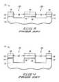
- Wafer fragment 10comprises a semiconductive material 12 upon which is formed a layer of oxide 14 , a layer of nitride 16 , and a patterned layer of photoresist 18 .
- Semiconductive material 12commonly comprises monocrystalline silicon which is lightly doped with a conductivity-enhancing dopant.
- semiconductive substrateis defined to mean any construction comprising semiconductive material, including, but not limited to, bulk semiconductive materials such as a semiconductive wafer (either alone or in assemblies comprising other materials thereon), and semiconductive material layers (either alone or in assemblies comprising other materials).
- substraterefers to any supporting structure, including, but not limited to, the semiconductive substrates described above.
- Oxide layer 14typically comprises silicon dioxide, and nitride layer 16 typically comprises silicon nitride.
- Oxide layer 14can consist essentially of silicon dioxide, and nitride layer 16 can consist essentially of silicon nitride.
- Nitride layer 16is generally from about 400 Angstroms thick to about 1500 Angstroms thick.
- patterned photoresist layer 18is used as a mask for an etching process.
- the etchis typically conducted utilizing dry plasma conditions and CH 2 F 2 /CF 4 chemistry. Such etching effectively etches both silicon nitride layer 16 and pad oxide layer 14 to form openings 20 extending therethrough. The etching stops upon reaching silicon substrate 12 .
- the etching into nitride layer 16defines upper corners 22 of the portions of the nitride layer remaining over substrate 12 .
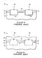
- a second etchis conducted to extend openings 20 into silicon substrate 12 .
- the second etchis commonly referred to as a “trench initiation etch.”
- the trench initiation etchis typically a timed dry plasma etch utilizing CF 4 /HBr, and typically extends openings 20 to less than or equal to about 500 Angstroms into substrate 12 .
- a third etchis conducted to extend openings 20 further into substrate 12 and thereby form trenches within substrate 12 .
- the third etchtypically utilizes an etchant consisting entirely of HBr, and is typically a timed etch. The timing of the etch is adjusted to form trenches within substrate 12 to a desired depth. For instance, if openings 20 are to be shallow trenches, the third etch will be timed to extend openings 20 to a depth of less than or equal to about one micron.
- photoresist layer 18( FIG. 4 ) is removed and a first oxide fill layer 24 is thermally grown within openings 20 .
- a high density plasma oxide 28is formed to fill openings 20 ( FIG. 5 ) and overlie nitride layer 16 .
- High density plasma oxide 28merges with oxide layer 24 ( FIG. 5 ) to form oxide plugs 30 within openings 20 (FIG. 5 ).
- wafer fragment 10is subjected to planarization (such as, for example, chemical-mechanical polishing) to planarize an upper surface of oxide plugs 30 .
- planarizationutilizes a chemistry selective for the oxide material of layer 24 ( FIG. 5 ) relative to the material of nitride layer 16 . Accordingly, nitride layer 16 functions as an etch-stop, and the planarization stops at an upper surface of nitride layer 16 .
- nitride layer 16is removed to expose pad oxide layer 14 between oxide plugs 30 .
- Subsequent processing(not shown) can then be conducted to form a polysilicon layer over and between oxide plugs 30 , and to form transistor devices from the polysilicon layer.
- the regions between oxide plugs 30are active regions for such transistor devices, and oxide plugs 30 are trench isolation regions separating the transistor devices.
- FIG. 9illustrates a top view of wafer fragment 10 at the processing step shown in FIG. 7 .
- FIG. 9illustrates a top view of wafer fragment 10 after a planarization process.
- Planarization processestypically comprise polishing processes wherein an abrasive material is rubbed against a layer that is to be planarized.
- chemical-mechanical polishing of oxide material 28involves rubbing a grit-containing slurry against oxide material 28 .
- the slurryis intended to form an interface between a polishing pad and wafer fragment 10 such that the pad does not physically contact portions of wafer fragment 10 .
- portions of the etch stopping layer, along with portions of the substratecan be chipped away. This can result in defects which render the device to be made inoperable.
- FIG. 9illustrates that the planarization process has chipped corners 22 of nitride layers 16 to remove portions of the nitride layers and form divots 40 .
- Some of the nitride chipped from corners 22has become lodged between the polishing pad and wafer fragment 10 during the planarization process.
- Divots 40 and scratches 42damage oxide regions 30 and can adversely impact further processing and utilization of wafer fragment 10 . Accordingly, it would be desirable to develop methods which alleviate chipping of etch-stop layers during planarization processes.
- the inventionencompasses a method of forming a material within an opening.
- An etch-stop layeris formed over a substrate.
- the etch-stop layerhas an opening extending therethrough to expose a portion of the underlying substrate and comprises an upper corner at a periphery of the opening.
- the upper cornerhas a corner angle with a first degree of sharpness. A portion of the upper corner is removed to reduce the sharpness of the corner angle to a second degree. After the portion of the upper corner is removed, a layer of material is formed within the opening and over the etch-stop layer.
- the materialis planarized with a method selective for the material relative to the etch-stop layer to remove the material from over the etch-stop layer while leaving the material within the opening.
- the inventionencompasses a method of forming an isolation region.
- a nitride-containing layeris formed over a semiconductor substrate.
- An openingis formed to extend through the nitride-containing layer and into the underlying substrate.
- the nitride-containing layercomprises an upper corner at a periphery of the opening.
- the upper cornerhas a corner angle with a first degree of sharpness.
- a portion of the upper corneris removed to reduce the sharpness of the corner angle to a second degree.
- an insulative materialis formed within the opening and over the nitride-containing layer.
- the insulative materialis planarized to remove the material from over the nitride-containing layer while leaving the material within the opening in the semiconductive substrate.
- the material within the opening in the semiconductive substrateforms at least a portion of an isolation region.
- FIG. 1is a diagrammatic, fragmentary, cross-sectional view of a semiconductor wafer fragment at a preliminary step of a prior art processing sequence.
- FIG. 2shows the FIG. 1 wafer fragment at a prior art processing step subsequent to that of FIG. 1 .
- FIG. 3shows the FIG. 1 wafer fragment at a prior art processing step subsequent to that of FIG. 2 .
- FIG. 4shows the FIG. 1 wafer fragment at a prior art processing step subsequent to that of FIG. 3 .
- FIG. 5shows the FIG. 1 wafer fragment at a prior art processing step subsequent to that of FIG. 4 .
- FIG. 6shows the FIG. 1 wafer fragment at a prior art processing step subsequent to that of FIG. 5 .
- FIG. 7shows the FIG. 1 wafer fragment at a prior art processing step subsequent to that of FIG. 6 .
- FIG. 8shows the FIG. 1 wafer fragment at a prior art processing step subsequent to that of FIG. 7 .
- FIG. 9shows a top view of the FIG. 1 wafer fragment at a prior art processing step identical to that shown in FIG. 7 .
- FIG. 10is a diagrammatic, fragmentary, cross-sectional view of a semiconductor wafer fragment processed according to a first embodiment method of the present invention.
- FIG. 11is a diagrammatic, fragmentary, cross-sectional view of a semiconductor wafer fragment processed according to a second embodiment method of the present invention.
- FIG. 12is a diagrammatic, fragmentary, cross-sectional view of a semiconductor wafer fragment processed according to a third embodiment method of the present invention.
- FIG. 13shows the FIG. 12 wafer fragment at a processing step subsequent to that of FIG. 12 .
- FIG. 14shows the FIG. 12 wafer fragment at a processing step subsequent to that of FIG. 13 .
- FIG. 10A first embodiment method of the present invention is described with reference to FIG. 10 .
- similar numbering to that utilized above in describing FIGS. 1-9is used, with differences indicated by the suffix “a” or by different numerals.
- a semiconductor wafer fragment 10 ais illustrated in FIG. 10 at a processing step subsequent to the prior art processing step illustrated in FIG. 5 .
- Wafer fragment 10 acomprises a substrate 12 , a pad oxide layer 14 , and an etch-stop layer 16 overlying oxide layer 14 .
- Etch-stop layer 16 acan comprise identical materials as etch-stop layer 16 of FIG. 5 , such as, for example, silicon nitride.
- Wafer fragment 10 adiffers from the wafer fragment 10 of FIG. 5 in that nitride-containing etch-stop layer 16 ( FIG. 5 ) has been subjected to a facet etch to reduce a sharpness of corners 22 ( FIG. 5 ) and form etch-stop layer 16 a of FIG. 5 .
- corners 22 of FIG. 5have a first degree of sharpness (shown as about a 90° angle).
- etch-stop layer 16 acomprises a facet 50 in place of corner 22 (FIG. 5 ), and has effectively replaced corner 22 with a pair of corners 52 and 54 .
- Each of corners 52 and 54comprises an angle greater than the about 90° angle of corner 22 (FIG. 5 ).
- the facet-etching of the exemplary first embodiment processinghas effectively removed a portion of upper corner 22 ( FIG. 5 ) to reduce a sharpness of the corner angle from a first degree (here about 90°) to a second degree (which here comprises an angle of greater than 90°).
- the layercan be facet-etched by, for example, a plasma etch utilizing argon.
- An exemplary pressure to which wafer fragment 10 a is subjected during flow of argon gas into the reaction chamberbeing from about 10 to about 100 standard cubic centimeters per minute, and with about 50 standard cubic centimeters per minute being typical.
- Power within the reaction chambercan be from about 100 watts to about 1,000 watts as a power at a top of the chamber, and from about 0 watts to about 1,000 watts as a power at a bottom of the chamber.
- a chuck temperature within the reaction chambercan float to about 400° C.
- the reaction chambercan be, for example, either a dual source plasma etcher or a single source plasma etcher.
- a fluorine-containing compoundsuch as, for example, CF 4
- fluorine-containing compoundcan volatilize nitride material during the facet etch such that the material will not otherwise deposit in openings 20 .
- the facet etchingcan be conducted in a completely separate etch step from the step of removal of photoresist layer 18 (FIG. 4 ), or as a continuation of a photoresist stripping etch.
- photoresist layer 18can be removed by, for example, an etch utilizing gas mixtures including O 2 , CF 4 and/or inert gas such as N 2 or Ar, which would also etch nitride layer 16 a to form facets 50 .
- facets 50Similar processing to that described above with reference to FIGS. 6-8 can be conducted to form a material (such as, for example, an oxide) over etch-stop layer 16 and within openings 20 , and to planarize the material.
- a materialsuch as, for example, an oxide
- the facet etching of nitride layer 16reduces the possibility that corners of etch-stop layer 16 will be chipped during planarization (such as, for example, chemical-mechanical polishing) of the material from over etch-stop layer 16 . Accordingly, the facet etching of the present invention can alleviate or eliminate the chipping and scratching problems of the prior art that were discussed above with reference to FIG. 9 .
- nitride layer 16 acan lead to overhanging oxide ledges (not shown) of isolation oxide formed within openings 20 during application of the subsequent processing of FIGS. 6-8 to the structure of FIG. 10 .
- overhanging oxide ledgescan result after nitride layer 16 a is removed in processing analogous to that described above with reference to FIG. 8 . If such overhanging oxide ledges are formed, they are preferably removed prior to formation of transistor devices proximate the isolation oxide.
- the overhanging oxide ledgescan be removed by, for example, chemical-mechanical polishing of the isolation oxide or appropriate wet chemical treatments.
- FIG. 11A second embodiment of the present invention is described with reference to FIG. 11 .
- similar numbering to that utilized above in describing prior art FIGS. 1-9is used, with differences indicated by the suffix “b”, or by different numerals.
- FIG. 11illustrates a semiconductor wafer fragment 10 b at a processing step subsequent to the prior art step illustrated in FIG. 5 .
- Wafer fragment 10 bcomprises a substrate 12 , a pad oxide layer 14 , and an etch-stop layer 16 b.
- Etch-stop layer 16 bcan comprise identical materials as etch-stop layer 16 of FIG. 5 , such as, for example, silicon nitride.
- Wafer fragment 10 bdiffers from wafer fragment 10 of FIG. 5 in that etch-stop layer 16 of FIG. 5 has been subjected to an anisotropic etch to round corners 22 ( FIG. 5 ) and form rounded corners 60 of etch-stop layer 16 b .
- the anisotropic etchcan comprise, for example, an etch utilizing CF 4 /CHF 3 , a power of greater than 0 and less than about 1000 watts, a temperature of less than about 50° C., and a pressure of less than about 300 mTorr.
- the anisotropic etching of layer 16 bremoves a portion of corner 22 ( FIG. 5 ) to reduce a sharpness of the corner.
- the anisotropic etchingreduces a corner angle of etch-stop layer 16 from a first degree of sharpness (corresponding to the sharpness of corner 22 of etch-stop layer 16 in FIG. 5 ) to a second degree of sharpness (corresponding to the rounded features of corners 60 etch-stop layer 16 b of FIG. 11 ).
- wafer fragment 10 bcan be subjected to subsequent processing similar to that described above with reference to FIGS. 6-8 to form a material (such as, for example, silicon dioxide) within openings 20 and over etch-stop layer 16 b , and to subsequently planarize the material down to an upper surface of etch-stop layer 16 b .
- Etch-stop layer 16 bcan then be removed, and the material utilized for forming isolation regions between transistor devices.
- nitride layer 16 bcan lead to overhanging oxide ledges (not shown) of isolation oxide formed during application of the subsequent processing of FIGS. 6-8 to the structure of FIG. 11 . If such overhanging oxide ledges are formed, they are preferably removed prior to formation of transistor devices adjacent the isolation oxide. Such overhanging oxide ledges can be removed by, for example, chemical-mechanical polishing of the isolation oxide after removal of etch-stop layer 16 b.
- corners 22can be rounded by etching processes other than the anisotropic etch described above.
- corners 22can be rounded by exposing a nitride-containing layer 16 ( FIG. 5 ) to a dip in hot phosphoric acid.
- Exemplary conditions for such hot phosphoric acid dipinclude a phosphoric acid solution having a concentration of about 86% (by weight), a temperature of the phosphoric acid of about 155° C., atmospheric pressure, and a dip time of from about 30 seconds to about 3 minutes.
- FIGS. 12-14A third embodiment of the present invention is discussed with reference to FIGS. 12-14 .
- similar numbering to that utilized above in describing the prior art processing of FIGS. 1-9is used, with differences indicated by the suffix “c” or by different numbers.
- FIG. 12illustrates a semiconductor wafer fragment 10 c at a processing step similar to the prior art processing step of FIG. 1.
- wafer fragment 10 c of FIG. 12comprises an etch-stop layer 16 c having two distinct portions
- wafer fragment 10comprises an etch-stop layer 16 containing only one portion.
- the two portions of etch-stop layer 16 care an upper portion 70 and a lower portion 72 .
- upper portion 70has a faster etch rate when exposed to subsequent etching conditions than does lower portion 72 .
- upper portion 70can comprise Si x N y O z , wherein x, y and z are greater than zero, and lower portion 72 can consist essentially of SiN. Upper portion 70 will then etch faster relative to lower portion 72 under subsequent etching conditions comprising exposing nitride-containing layer 16 c to hydrofluoric acid.
- a lower portion 72 consisting essentially of SiNcan be formed by, for example, chemical vapor deposition utilizing SiH 2 Cl 2 and NH 3 .
- Upper portion 70 comprising Si x N y O zcan then be formed by, for example, chemical vapor deposition utilizing SiH 2 Cl 2 , NH 3 and N 2 O.
- upper portion Si x N y O zcan be formed by oxidizing an upper surface of silicon nitride lower portion 72 .
- Such oxidationcan comprise, for example, rapid thermal processing at a temperature of from about 1,000° C. to about 1,100° C. in an oxidizing ambient (e.g., O 2 , NO x , H 2 O 2 , etc.) for a time of from about 30 seconds to about three minutes.
- an oxidizing ambiente.g., O 2 , NO x , H 2 O 2 , etc.
- Lower portion 72is formed by chemical vapor deposition utilizing SiH 2 Cl 2 and NH 3 as precursors, in a reaction chamber at a temperature of from about 650° C. to about 800° C., and at a pressure of from about 100 mTorr to about 500 mTorr.
- N 2 Ois introduced into the reaction chamber as another precursor.
- the combination of N 2 O, SiH 2 Cl 2 and NH 3 precursorsgrows upper layer 70 comprising Si x N y O z .
- lower portion 72 of nitride layer 16 cis formed to a thickness of from greater than 0 Angstroms to about 900 Angstroms, and upper portion 70 is formed to a thickness of from about 50 Angstroms to about 500 Angstroms.
- a hydrofluoric acid etch of layer 16 cis described with reference to FIGS. 13 and 14 .
- wafer fragment 12is subjected to processing analogous to the processing described above with reference to FIGS. 2-5 , to form openings 20 extending through etch-stop layer 16 c and into substrate 12 .
- Etch-stop layer 16 ccomprises upper corners 74 having a first degree of roughness.
- wafer fragment 10 cis subjected to a dip in hydrofluoric acid solution which rounds corners 74 ( FIG. 13 ) to form corners 76 having a second degree of sharpness which is less than the first degree of sharpness of corners 74 .
- wafer fragment 10 ccan be subjected to the processing of FIGS. 6-8 to form isolation regions analogous to isolation regions 30 of FIG. 8 .
- Rounded corners 76can avoid the prior art chipping and scratching problems discussed above with reference to FIG. 9 .
- lower portion 72can comprise silicon nitride comprising a first stoichiometric amount of silicon
- upper portion 72can comprise silicon nitride comprising a second stoichiometric amount of silicon that is greater than the first stoichiometric amount of silicon.
- Upper portion 70will then etch faster than lower portion 72 when nitride layer 16 c is exposed to planarizing conditions, such as the conditions described above with reference to prior art FIG. 7.
- a method of forming such nitride layer 16 c comprising a first stoichiometric amount of silicon in lower portion 72 and a second stoichiometric amount of silicon in upper portion 70is as follows.
- a chemical vapor deposition (CVD) processis utilized with a silicon precursor gas (for example SiH 2 Cl 2 (dichlorosilane)) and a nitrogen precursor gas (for example, NH 3 (ammonia)).
- a substrateis provided within a CVD reaction chamber, together with a first ratio of the silicon precursor gas to the nitrogen precursor gas.
- the first ratio of the silicon precursor gas to the nitrogen precursor gascan be about 0.33 to form a lower portion 72 having a stoichiometry of about Si 3 N 4 .
- the ratio of the silicon precursor gas to the nitrogen precursor gasis raised to, for example, about 6 to form a silicon enriched upper portion 72 of the silicon nitride layer.
- the silicon enriched upper portionhas a stoichiometry of Si x N y , wherein the ratio of x to y is greater than or equal to 1.
- the silicon enriched upper portioncan comprise, for example, Si 4 N 4 , Si 7 N 4 , Si 10 N 1 , or, if the flow of nitrogen precursor gas is effectively ceased, Si.
- Exemplary processing conditions for the CVD processcan include a pressure of from about 100 mTorr to about 1 Torr, and a temperature of from about 700° C. to about 800° C.
- etch-stop layer 16 c of silicon nitrideis to form lower portion 72 from silicon nitride utilizing chemical vapor deposition of SiH 2 Cl 2 and NH 3 without a plasma, and to form upper portion 70 utilizing plasma enhanced chemical vapor deposition in the presence of an oxygen-containing precursor, SiH 4 and NH 3 .
- Lower portion 72can then consist essentially of silicon and nitrogen, and upper portion 70 can then comprise Si x N y O z wherein x, y and z are greater than 1.
- such upper portionis more rapidly etched by a hydrofluoric acid etch than is such lower portion.
Landscapes
- Engineering & Computer Science (AREA)
- Physics & Mathematics (AREA)
- Condensed Matter Physics & Semiconductors (AREA)
- General Physics & Mathematics (AREA)
- Manufacturing & Machinery (AREA)
- Computer Hardware Design (AREA)
- Microelectronics & Electronic Packaging (AREA)
- Power Engineering (AREA)
- Element Separation (AREA)
- Drying Of Semiconductors (AREA)
Abstract
Description
Claims (13)
Priority Applications (2)
| Application Number | Priority Date | Filing Date | Title |
|---|---|---|---|
| US10/145,562US6884725B2 (en) | 1998-09-03 | 2002-05-14 | Methods of forming materials within openings, and methods of forming isolation regions |
| US11/115,833US7358587B2 (en) | 1998-09-03 | 2005-04-25 | Semiconductor structures |
Applications Claiming Priority (3)
| Application Number | Priority Date | Filing Date | Title |
|---|---|---|---|
| US09/146,730US6274498B1 (en) | 1998-09-03 | 1998-09-03 | Methods of forming materials within openings, and method of forming isolation regions |
| US09/910,340US6420268B2 (en) | 1998-09-03 | 2001-07-20 | Methods of forming materials within openings, and methods of forming isolation regions |
| US10/145,562US6884725B2 (en) | 1998-09-03 | 2002-05-14 | Methods of forming materials within openings, and methods of forming isolation regions |
Related Parent Applications (1)
| Application Number | Title | Priority Date | Filing Date |
|---|---|---|---|
| US09/910,340ContinuationUS6420268B2 (en) | 1998-09-03 | 2001-07-20 | Methods of forming materials within openings, and methods of forming isolation regions |
Related Child Applications (1)
| Application Number | Title | Priority Date | Filing Date |
|---|---|---|---|
| US11/115,833ContinuationUS7358587B2 (en) | 1998-09-03 | 2005-04-25 | Semiconductor structures |
Publications (2)
| Publication Number | Publication Date |
|---|---|
| US20020132483A1 US20020132483A1 (en) | 2002-09-19 |
| US6884725B2true US6884725B2 (en) | 2005-04-26 |
Family
ID=22518743
Family Applications (4)
| Application Number | Title | Priority Date | Filing Date |
|---|---|---|---|
| US09/146,730Expired - LifetimeUS6274498B1 (en) | 1998-09-03 | 1998-09-03 | Methods of forming materials within openings, and method of forming isolation regions |
| US09/910,340Expired - LifetimeUS6420268B2 (en) | 1998-09-03 | 2001-07-20 | Methods of forming materials within openings, and methods of forming isolation regions |
| US10/145,562Expired - LifetimeUS6884725B2 (en) | 1998-09-03 | 2002-05-14 | Methods of forming materials within openings, and methods of forming isolation regions |
| US11/115,833Expired - Fee RelatedUS7358587B2 (en) | 1998-09-03 | 2005-04-25 | Semiconductor structures |
Family Applications Before (2)
| Application Number | Title | Priority Date | Filing Date |
|---|---|---|---|
| US09/146,730Expired - LifetimeUS6274498B1 (en) | 1998-09-03 | 1998-09-03 | Methods of forming materials within openings, and method of forming isolation regions |
| US09/910,340Expired - LifetimeUS6420268B2 (en) | 1998-09-03 | 2001-07-20 | Methods of forming materials within openings, and methods of forming isolation regions |
Family Applications After (1)
| Application Number | Title | Priority Date | Filing Date |
|---|---|---|---|
| US11/115,833Expired - Fee RelatedUS7358587B2 (en) | 1998-09-03 | 2005-04-25 | Semiconductor structures |
Country Status (1)
| Country | Link |
|---|---|
| US (4) | US6274498B1 (en) |
Cited By (4)
| Publication number | Priority date | Publication date | Assignee | Title |
|---|---|---|---|---|
| US20040121552A1 (en)* | 2002-12-20 | 2004-06-24 | Young-Hun Seo | Method of forming trench in semiconductor device |
| US20060160326A1 (en)* | 2004-12-29 | 2006-07-20 | Lee Yong J | Method for rounding top corners of isolation trench in semiconductor device |
| US20120309166A1 (en)* | 2011-05-31 | 2012-12-06 | United Microelectronics Corp. | Process for forming shallow trench isolation structure |
| US9558989B2 (en)* | 2014-07-10 | 2017-01-31 | Renesas Electronics Corporation | Method for manufacturing semiconductor device |
Families Citing this family (19)
| Publication number | Priority date | Publication date | Assignee | Title |
|---|---|---|---|---|
| US6274498B1 (en)* | 1998-09-03 | 2001-08-14 | Micron Technology, Inc. | Methods of forming materials within openings, and method of forming isolation regions |
| US6372601B1 (en) | 1998-09-03 | 2002-04-16 | Micron Technology, Inc. | Isolation region forming methods |
| KR100761637B1 (en)* | 1999-03-03 | 2007-09-27 | 엘피다 메모리, 아이엔씨. | Semiconductor integrated circuit device and manufacturing method thereof |
| US6204149B1 (en)* | 1999-05-26 | 2001-03-20 | Micron Technology, Inc. | Methods of forming polished material and methods of forming isolation regions |
| JP3917327B2 (en)* | 1999-06-01 | 2007-05-23 | 株式会社ルネサステクノロジ | Method and apparatus for manufacturing semiconductor device |
| WO2001018866A1 (en)* | 1999-09-10 | 2001-03-15 | Starmega Corporation | Strongly textured atomic ridges and dots |
| TW506105B (en)* | 2001-10-26 | 2002-10-11 | Nanya Technology Corp | Method for forming interconnect |
| JP2003142573A (en)* | 2001-10-31 | 2003-05-16 | Seiko Epson Corp | Method for manufacturing semiconductor device |
| US6599205B1 (en)* | 2002-02-07 | 2003-07-29 | Ryan F. Andrews | Combination ball marker and turf repair golf tool promotional device |
| JP3637332B2 (en)* | 2002-05-29 | 2005-04-13 | 株式会社東芝 | Semiconductor device and manufacturing method thereof |
| US6716719B2 (en)* | 2002-05-29 | 2004-04-06 | Micron Technology, Inc. | Method of forming biasable isolation regions using epitaxially grown silicon between the isolation regions |
| JP4770360B2 (en)* | 2005-09-26 | 2011-09-14 | 富士通株式会社 | CAD program, CAD apparatus and CAD system for performing projection control processing |
| US20090184402A1 (en)* | 2008-01-22 | 2009-07-23 | United Microelectronics Corp. | Method of fabricating a shallow trench isolation structure including forming a second liner covering the corner of the trench and first liner. |
| CN102074495B (en)* | 2009-11-20 | 2013-10-09 | 中芯国际集成电路制造(上海)有限公司 | Forming method for shallow trench isolation (STI) |
| US8409257B2 (en) | 2010-11-10 | 2013-04-02 | Warsaw Othopedic, Inc. | Systems and methods for facet joint stabilization |
| CN103137487B (en)* | 2011-11-30 | 2016-02-10 | 上海华虹宏力半导体制造有限公司 | The method that passivation of deep trench corner is improved |
| CN103515214A (en)* | 2012-06-25 | 2014-01-15 | 中芯国际集成电路制造(上海)有限公司 | Manufacturing method of semiconductor device |
| CN104517887B (en)* | 2013-09-27 | 2018-07-20 | 中芯国际集成电路制造(上海)有限公司 | A method of making semiconductor devices |
| TWI685061B (en)* | 2016-05-04 | 2020-02-11 | 聯華電子股份有限公司 | Semiconductor device and method for fabricating the same |
Citations (62)
| Publication number | Priority date | Publication date | Assignee | Title |
|---|---|---|---|---|
| US4533430A (en) | 1984-01-04 | 1985-08-06 | Advanced Micro Devices, Inc. | Process for forming slots having near vertical sidewalls at their upper extremities |
| US4534826A (en)* | 1983-12-29 | 1985-08-13 | Ibm Corporation | Trench etch process for dielectric isolation |
| US4663832A (en) | 1984-06-29 | 1987-05-12 | International Business Machines Corporation | Method for improving the planarity and passivation in a semiconductor isolation trench arrangement |
| US4882291A (en) | 1987-01-26 | 1989-11-21 | Commissiriat A L'energie Atomique | Process for the production of electrical isolation zones in a CMOS integrated circuit |
| US5258332A (en) | 1987-08-28 | 1993-11-02 | Kabushiki Kaisha Toshiba | Method of manufacturing semiconductor devices including rounding of corner portions by etching |
| US5356828A (en) | 1993-07-01 | 1994-10-18 | Digital Equipment Corporation | Method of forming micro-trench isolation regions in the fabrication of semiconductor devices |
| US5374585A (en) | 1994-05-09 | 1994-12-20 | Motorola, Inc. | Process for forming field isolation |
| US5397733A (en) | 1993-05-21 | 1995-03-14 | Hyundai Electronics Industries Co., Ltd. | Method for the construction of field oxide film in semiconductor device |
| US5399520A (en) | 1993-03-31 | 1995-03-21 | Hyundai Electronics Industries Co., Ltd. | Method for the formation of field oxide film in semiconductor device |
| US5506168A (en) | 1992-10-27 | 1996-04-09 | Kabushiki Kaisha Toshiba | Method for manufacturing semiconductor device |
| US5554256A (en) | 1993-09-23 | 1996-09-10 | U.S. Philips Corporation | Method of manufacturing a semiconductor device having a semiconductor body with field insulation regions formed by grooves filled with insulating material |
| US5578518A (en) | 1993-12-20 | 1996-11-26 | Kabushiki Kaisha Toshiba | Method of manufacturing a trench isolation having round corners |
| EP0782185A2 (en) | 1995-12-25 | 1997-07-02 | Nec Corporation | Process of fabricating semiconductor device having isolating oxide rising out of groove |
| US5674775A (en) | 1997-02-20 | 1997-10-07 | Taiwan Semiconductor Manufacturing Company, Ltd. | Isolation trench with a rounded top edge using an etch buffer layer |
| US5712185A (en) | 1996-04-23 | 1998-01-27 | United Microelectronics | Method for forming shallow trench isolation |
| US5728620A (en) | 1995-04-21 | 1998-03-17 | Samsung Electronics Co., Ltd. | Isolation method of semiconductor device |
| US5780346A (en) | 1996-12-31 | 1998-07-14 | Intel Corporation | N2 O nitrided-oxide trench sidewalls and method of making isolation structure |
| US5801083A (en) | 1997-10-20 | 1998-09-01 | Chartered Semiconductor Manufacturing, Ltd. | Use of polymer spacers for the fabrication of shallow trench isolation regions with rounded top corners |
| US5817566A (en)* | 1997-03-03 | 1998-10-06 | Taiwan Semiconductor Manufacturing Company, Ltd. | Trench filling method employing oxygen densified gap filling silicon oxide layer formed with low ozone concentration |
| US5834358A (en) | 1996-11-12 | 1998-11-10 | Micron Technology, Inc. | Isolation regions and methods of forming isolation regions |
| US5843846A (en)* | 1996-12-31 | 1998-12-01 | Intel Corporation | Etch process to produce rounded top corners for sub-micron silicon trench applications |
| US5858865A (en) | 1995-12-07 | 1999-01-12 | Micron Technology, Inc. | Method of forming contact plugs |
| US5863827A (en) | 1997-06-03 | 1999-01-26 | Texas Instruments Incorporated | Oxide deglaze before sidewall oxidation of mesa or trench |
| JPH1167890A (en) | 1997-08-22 | 1999-03-09 | Sharp Corp | Method for manufacturing semiconductor device |
| US5880004A (en) | 1997-06-10 | 1999-03-09 | Winbond Electronics Corp. | Trench isolation process |
| US5895254A (en) | 1997-10-09 | 1999-04-20 | United Microelectronics Corp. | Method of manufacturing shallow trench isolation structure |
| US5904538A (en) | 1997-03-24 | 1999-05-18 | Lg Semicon Co., Ltd | Method for developing shallow trench isolation in a semiconductor memory device |
| US5904523A (en)* | 1996-10-03 | 1999-05-18 | Lucent Technologies Inc. | Process for device fabrication in which a layer of oxynitride is formed at low temperatures |
| US5926722A (en)* | 1997-04-07 | 1999-07-20 | Taiwan Semiconductor Manufacturing Co., Ltd. | Planarization of shallow trench isolation by differential etchback and chemical mechanical polishing |
| US5925575A (en) | 1997-09-29 | 1999-07-20 | Taiwan Semiconductor Manufacturing Company, Ltd. | Dry etching endpoint procedure to protect against photolithographic misalignments |
| US5933749A (en) | 1997-10-27 | 1999-08-03 | United Microelectronics Corp. | Method for removing a top corner of a trench |
| US5937308A (en) | 1997-03-26 | 1999-08-10 | Advanced Micro Devices, Inc. | Semiconductor trench isolation structure formed substantially within a single chamber |
| US5960297A (en) | 1997-07-02 | 1999-09-28 | Kabushiki Kaisha Toshiba | Shallow trench isolation structure and method of forming the same |
| US5962342A (en) | 1997-10-27 | 1999-10-05 | United Microelectronics Corporation | Adjustable method for eliminating trench top corners |
| US5966614A (en) | 1996-12-17 | 1999-10-12 | Samsung Electronics Co., Ltd. | Silicon nitride-free isolation methods for integrated circuits |
| US5968842A (en)* | 1997-09-12 | 1999-10-19 | United Semiconductor Corp. | Techniques for reduced dishing in chemical mechanical polishing |
| US5976948A (en) | 1998-02-19 | 1999-11-02 | Advanced Micro Devices | Process for forming an isolation region with trench cap |
| US5981356A (en) | 1997-07-28 | 1999-11-09 | Integrated Device Technology, Inc. | Isolation trenches with protected corners |
| US5989975A (en) | 1997-10-04 | 1999-11-23 | United Microelectronics Corp. | Method for manufacturing shallow trench isolation |
| US6010947A (en) | 1996-07-16 | 2000-01-04 | Kabushiki Kaisha Toshiba | Semiconductor device and method for manufacturing |
| US6040232A (en) | 1998-11-06 | 2000-03-21 | United Semiconductor Corp. | Method of manufacturing shallow trench isolation |
| US6074932A (en) | 1998-01-28 | 2000-06-13 | Texas Instruments - Acer Incorporated | Method for forming a stress-free shallow trench isolation |
| US6083808A (en) | 1997-09-25 | 2000-07-04 | Samsung Electronics Co., Ltd. | Method for forming a trench isolation in a semiconductor device |
| US6090683A (en) | 1997-06-16 | 2000-07-18 | Micron Technology, Inc. | Method of etching thermally grown oxide substantially selectively relative to deposited oxide |
| US6090684A (en) | 1998-07-31 | 2000-07-18 | Hitachi, Ltd. | Method for manufacturing semiconductor device |
| US6093621A (en) | 1999-04-05 | 2000-07-25 | Vanguard International Semiconductor Corp. | Method of forming shallow trench isolation |
| US6100160A (en) | 1998-02-17 | 2000-08-08 | Texas Instruments Incorporated | Oxide etch barrier formed by nitridation |
| US6103635A (en) | 1997-10-28 | 2000-08-15 | Fairchild Semiconductor Corp. | Trench forming process and integrated circuit device including a trench |
| US6121113A (en) | 1997-06-30 | 2000-09-19 | Fujitsu Limited | Method for production of semiconductor device |
| JP2000269318A (en) | 1999-03-12 | 2000-09-29 | Toshiba Corp | Semiconductor device and manufacturing method thereof |
| US6153478A (en) | 1998-01-28 | 2000-11-28 | United Microelectronics Corp. | STI process for eliminating kink effect |
| US6153480A (en) | 1998-05-08 | 2000-11-28 | Intel Coroporation | Advanced trench sidewall oxide for shallow trench technology |
| US6177331B1 (en) | 1997-06-04 | 2001-01-23 | Nec Corporation | Method for manufacturing semiconductor device |
| US6232203B1 (en) | 1999-07-23 | 2001-05-15 | Taiwan Semiconductor Manufacturing Company | Process for making improved shallow trench isolation by employing nitride spacers in the formation of the trenches |
| US6238999B1 (en) | 1998-09-03 | 2001-05-29 | Micron Technology | Isolation region forming methods |
| US6245684B1 (en) | 1998-03-13 | 2001-06-12 | Applied Materials, Inc. | Method of obtaining a rounded top trench corner for semiconductor trench etch applications |
| US6245640B1 (en) | 1998-09-25 | 2001-06-12 | Siemens Aktiengesellschaft | Method for fabricating a semiconductor structure |
| US6249035B1 (en) | 1998-02-02 | 2001-06-19 | Chartered Semiconductor Manufacturing Ltd. | LOCOS mask for suppression of narrow space field oxide thinning and oxide punch through effect |
| US6274498B1 (en)* | 1998-09-03 | 2001-08-14 | Micron Technology, Inc. | Methods of forming materials within openings, and method of forming isolation regions |
| US6284625B1 (en) | 1998-11-09 | 2001-09-04 | Hitachi, Ltd. | Method of forming a shallow groove isolation structure |
| US6284623B1 (en) | 1999-10-25 | 2001-09-04 | Peng-Fei Zhang | Method of fabricating semiconductor devices using shallow trench isolation with reduced narrow channel effect |
| US6287921B1 (en) | 1999-10-12 | 2001-09-11 | Vanguard International Semiconductor Corporation | Method of performing threshold voltage adjustment for MOS transistors |
Family Cites Families (12)
| Publication number | Priority date | Publication date | Assignee | Title |
|---|---|---|---|---|
| US5248350A (en)* | 1990-11-30 | 1993-09-28 | Ncr Corporation | Structure for improving gate oxide integrity for a semiconductor formed by a recessed sealed sidewall field oxidation process |
| JPH09129720A (en) | 1995-11-06 | 1997-05-16 | Sony Corp | Manufacture of trench-isolated separated semiconductor device |
| JPH10308442A (en) | 1997-05-07 | 1998-11-17 | Mitsubishi Electric Corp | Method for manufacturing semiconductor device |
| US5801082A (en)* | 1997-08-18 | 1998-09-01 | Vanguard International Semiconductor Corporation | Method for making improved shallow trench isolation with dielectric studs for semiconductor integrated circuits |
| US6002160A (en)* | 1997-12-12 | 1999-12-14 | Advanced Micro Devices, Inc. | Semiconductor isolation process to minimize weak oxide problems |
| US6599810B1 (en)* | 1998-11-05 | 2003-07-29 | Advanced Micro Devices, Inc. | Shallow trench isolation formation with ion implantation |
| KR100322531B1 (en)* | 1999-01-11 | 2002-03-18 | 윤종용 | Method for Trench Isolation using a Dent free layer &Semiconductor Device thereof |
| US6027982A (en)* | 1999-02-05 | 2000-02-22 | Chartered Semiconductor Manufacturing Ltd. | Method to form shallow trench isolation structures with improved isolation fill and surface planarity |
| EP1104936A1 (en)* | 1999-11-25 | 2001-06-06 | Mitsubishi Denki Kabushiki Kaisha | Method of manufacturing a semiconductor device, and semiconductor device manufactured thereby |
| US6368970B1 (en)* | 2000-08-24 | 2002-04-09 | Infineon Technologies Ag | Semiconductor configuration and corresponding production process |
| US6368941B1 (en)* | 2000-11-08 | 2002-04-09 | United Microelectronics Corp. | Fabrication of a shallow trench isolation by plasma oxidation |
| US6486038B1 (en)* | 2001-03-12 | 2002-11-26 | Advanced Micro Devices | Method for and device having STI using partial etch trench bottom liner |
- 1998
- 1998-09-03USUS09/146,730patent/US6274498B1/ennot_activeExpired - Lifetime
- 2001
- 2001-07-20USUS09/910,340patent/US6420268B2/ennot_activeExpired - Lifetime
- 2002
- 2002-05-14USUS10/145,562patent/US6884725B2/ennot_activeExpired - Lifetime
- 2005
- 2005-04-25USUS11/115,833patent/US7358587B2/ennot_activeExpired - Fee Related
Patent Citations (63)
| Publication number | Priority date | Publication date | Assignee | Title |
|---|---|---|---|---|
| US4534826A (en)* | 1983-12-29 | 1985-08-13 | Ibm Corporation | Trench etch process for dielectric isolation |
| US4533430A (en) | 1984-01-04 | 1985-08-06 | Advanced Micro Devices, Inc. | Process for forming slots having near vertical sidewalls at their upper extremities |
| US4663832A (en) | 1984-06-29 | 1987-05-12 | International Business Machines Corporation | Method for improving the planarity and passivation in a semiconductor isolation trench arrangement |
| US4882291A (en) | 1987-01-26 | 1989-11-21 | Commissiriat A L'energie Atomique | Process for the production of electrical isolation zones in a CMOS integrated circuit |
| US5258332A (en) | 1987-08-28 | 1993-11-02 | Kabushiki Kaisha Toshiba | Method of manufacturing semiconductor devices including rounding of corner portions by etching |
| US5506168A (en) | 1992-10-27 | 1996-04-09 | Kabushiki Kaisha Toshiba | Method for manufacturing semiconductor device |
| US5399520A (en) | 1993-03-31 | 1995-03-21 | Hyundai Electronics Industries Co., Ltd. | Method for the formation of field oxide film in semiconductor device |
| US5397733A (en) | 1993-05-21 | 1995-03-14 | Hyundai Electronics Industries Co., Ltd. | Method for the construction of field oxide film in semiconductor device |
| US5356828A (en) | 1993-07-01 | 1994-10-18 | Digital Equipment Corporation | Method of forming micro-trench isolation regions in the fabrication of semiconductor devices |
| US5554256A (en) | 1993-09-23 | 1996-09-10 | U.S. Philips Corporation | Method of manufacturing a semiconductor device having a semiconductor body with field insulation regions formed by grooves filled with insulating material |
| US5578518A (en) | 1993-12-20 | 1996-11-26 | Kabushiki Kaisha Toshiba | Method of manufacturing a trench isolation having round corners |
| US5374585A (en) | 1994-05-09 | 1994-12-20 | Motorola, Inc. | Process for forming field isolation |
| US5728620A (en) | 1995-04-21 | 1998-03-17 | Samsung Electronics Co., Ltd. | Isolation method of semiconductor device |
| US5858865A (en) | 1995-12-07 | 1999-01-12 | Micron Technology, Inc. | Method of forming contact plugs |
| EP0782185A2 (en) | 1995-12-25 | 1997-07-02 | Nec Corporation | Process of fabricating semiconductor device having isolating oxide rising out of groove |
| US5677233A (en) | 1995-12-25 | 1997-10-14 | Nec Corporation | Process of fabricating semiconductor device having isolating oxide rising out of groove |
| US5712185A (en) | 1996-04-23 | 1998-01-27 | United Microelectronics | Method for forming shallow trench isolation |
| US6010947A (en) | 1996-07-16 | 2000-01-04 | Kabushiki Kaisha Toshiba | Semiconductor device and method for manufacturing |
| US5904523A (en)* | 1996-10-03 | 1999-05-18 | Lucent Technologies Inc. | Process for device fabrication in which a layer of oxynitride is formed at low temperatures |
| US5834358A (en) | 1996-11-12 | 1998-11-10 | Micron Technology, Inc. | Isolation regions and methods of forming isolation regions |
| US5966614A (en) | 1996-12-17 | 1999-10-12 | Samsung Electronics Co., Ltd. | Silicon nitride-free isolation methods for integrated circuits |
| US5780346A (en) | 1996-12-31 | 1998-07-14 | Intel Corporation | N2 O nitrided-oxide trench sidewalls and method of making isolation structure |
| US5843846A (en)* | 1996-12-31 | 1998-12-01 | Intel Corporation | Etch process to produce rounded top corners for sub-micron silicon trench applications |
| US5674775A (en) | 1997-02-20 | 1997-10-07 | Taiwan Semiconductor Manufacturing Company, Ltd. | Isolation trench with a rounded top edge using an etch buffer layer |
| US5817566A (en)* | 1997-03-03 | 1998-10-06 | Taiwan Semiconductor Manufacturing Company, Ltd. | Trench filling method employing oxygen densified gap filling silicon oxide layer formed with low ozone concentration |
| US5904538A (en) | 1997-03-24 | 1999-05-18 | Lg Semicon Co., Ltd | Method for developing shallow trench isolation in a semiconductor memory device |
| US5937308A (en) | 1997-03-26 | 1999-08-10 | Advanced Micro Devices, Inc. | Semiconductor trench isolation structure formed substantially within a single chamber |
| US5926722A (en)* | 1997-04-07 | 1999-07-20 | Taiwan Semiconductor Manufacturing Co., Ltd. | Planarization of shallow trench isolation by differential etchback and chemical mechanical polishing |
| US5863827A (en) | 1997-06-03 | 1999-01-26 | Texas Instruments Incorporated | Oxide deglaze before sidewall oxidation of mesa or trench |
| US6177331B1 (en) | 1997-06-04 | 2001-01-23 | Nec Corporation | Method for manufacturing semiconductor device |
| US5880004A (en) | 1997-06-10 | 1999-03-09 | Winbond Electronics Corp. | Trench isolation process |
| US6090683A (en) | 1997-06-16 | 2000-07-18 | Micron Technology, Inc. | Method of etching thermally grown oxide substantially selectively relative to deposited oxide |
| US6121113A (en) | 1997-06-30 | 2000-09-19 | Fujitsu Limited | Method for production of semiconductor device |
| US5960297A (en) | 1997-07-02 | 1999-09-28 | Kabushiki Kaisha Toshiba | Shallow trench isolation structure and method of forming the same |
| US5981356A (en) | 1997-07-28 | 1999-11-09 | Integrated Device Technology, Inc. | Isolation trenches with protected corners |
| JPH1167890A (en) | 1997-08-22 | 1999-03-09 | Sharp Corp | Method for manufacturing semiconductor device |
| US5968842A (en)* | 1997-09-12 | 1999-10-19 | United Semiconductor Corp. | Techniques for reduced dishing in chemical mechanical polishing |
| US6083808A (en) | 1997-09-25 | 2000-07-04 | Samsung Electronics Co., Ltd. | Method for forming a trench isolation in a semiconductor device |
| US5925575A (en) | 1997-09-29 | 1999-07-20 | Taiwan Semiconductor Manufacturing Company, Ltd. | Dry etching endpoint procedure to protect against photolithographic misalignments |
| US5989975A (en) | 1997-10-04 | 1999-11-23 | United Microelectronics Corp. | Method for manufacturing shallow trench isolation |
| US5895254A (en) | 1997-10-09 | 1999-04-20 | United Microelectronics Corp. | Method of manufacturing shallow trench isolation structure |
| US5801083A (en) | 1997-10-20 | 1998-09-01 | Chartered Semiconductor Manufacturing, Ltd. | Use of polymer spacers for the fabrication of shallow trench isolation regions with rounded top corners |
| US5933749A (en) | 1997-10-27 | 1999-08-03 | United Microelectronics Corp. | Method for removing a top corner of a trench |
| US5962342A (en) | 1997-10-27 | 1999-10-05 | United Microelectronics Corporation | Adjustable method for eliminating trench top corners |
| US6103635A (en) | 1997-10-28 | 2000-08-15 | Fairchild Semiconductor Corp. | Trench forming process and integrated circuit device including a trench |
| US6074932A (en) | 1998-01-28 | 2000-06-13 | Texas Instruments - Acer Incorporated | Method for forming a stress-free shallow trench isolation |
| US6153478A (en) | 1998-01-28 | 2000-11-28 | United Microelectronics Corp. | STI process for eliminating kink effect |
| US6249035B1 (en) | 1998-02-02 | 2001-06-19 | Chartered Semiconductor Manufacturing Ltd. | LOCOS mask for suppression of narrow space field oxide thinning and oxide punch through effect |
| US6100160A (en) | 1998-02-17 | 2000-08-08 | Texas Instruments Incorporated | Oxide etch barrier formed by nitridation |
| US5976948A (en) | 1998-02-19 | 1999-11-02 | Advanced Micro Devices | Process for forming an isolation region with trench cap |
| US6245684B1 (en) | 1998-03-13 | 2001-06-12 | Applied Materials, Inc. | Method of obtaining a rounded top trench corner for semiconductor trench etch applications |
| US6153480A (en) | 1998-05-08 | 2000-11-28 | Intel Coroporation | Advanced trench sidewall oxide for shallow trench technology |
| US6090684A (en) | 1998-07-31 | 2000-07-18 | Hitachi, Ltd. | Method for manufacturing semiconductor device |
| US6238999B1 (en) | 1998-09-03 | 2001-05-29 | Micron Technology | Isolation region forming methods |
| US6274498B1 (en)* | 1998-09-03 | 2001-08-14 | Micron Technology, Inc. | Methods of forming materials within openings, and method of forming isolation regions |
| US6245640B1 (en) | 1998-09-25 | 2001-06-12 | Siemens Aktiengesellschaft | Method for fabricating a semiconductor structure |
| US6040232A (en) | 1998-11-06 | 2000-03-21 | United Semiconductor Corp. | Method of manufacturing shallow trench isolation |
| US6284625B1 (en) | 1998-11-09 | 2001-09-04 | Hitachi, Ltd. | Method of forming a shallow groove isolation structure |
| JP2000269318A (en) | 1999-03-12 | 2000-09-29 | Toshiba Corp | Semiconductor device and manufacturing method thereof |
| US6093621A (en) | 1999-04-05 | 2000-07-25 | Vanguard International Semiconductor Corp. | Method of forming shallow trench isolation |
| US6232203B1 (en) | 1999-07-23 | 2001-05-15 | Taiwan Semiconductor Manufacturing Company | Process for making improved shallow trench isolation by employing nitride spacers in the formation of the trenches |
| US6287921B1 (en) | 1999-10-12 | 2001-09-11 | Vanguard International Semiconductor Corporation | Method of performing threshold voltage adjustment for MOS transistors |
| US6284623B1 (en) | 1999-10-25 | 2001-09-04 | Peng-Fei Zhang | Method of fabricating semiconductor devices using shallow trench isolation with reduced narrow channel effect |
Non-Patent Citations (8)
| Title |
|---|
| "Optimized shallow trench isolation Structure and its process for eliminating shallow trench isolation-induced parasitic effects" IBM Technical Disclosure Bulletin; vol. 34, No. 11; Apr. 1992; pps. 276-277. |
| Chatterjee, A., et al., A Study of Integration Issues in SHallow Trench Isolation for Deep Submicron CMOS Tecnologies, SPIE vol. 2875, Aug. 1996, pp. 39-43. |
| EP 0 782 185 A3 Search Report; Published Aug. 20, 1997; 2 pps. |
| Fazan et al., "A Highly Manufacturable Trench Isolation Process for Deep Submicron DRAMS," (C) 1993 IEEE, pp. 57-60 (4 pages). |
| Ishimaru et al., "Trench Isolation Technology with 1 mum Depth-13 and p-wells for A Full-CMOS SRAM Cell with a 0.4 mum n+/p+ Spacing." (C) IEEE, pp. 97-98. |
| S. Wolf et al, Silicon Processing for the VLSI Era, vol. 1, p. 366, 1986. |
| S. Wolfe et al, Silicon Processing for the VLSI Era, vol. 1, pps. 522, 534, 541, 1986. |
| Wolf Ph.D. "Silicon Processing for the VLSI Ero, vol. 2: Process Integration," (C)1990, pp. 51-54. |
Cited By (5)
| Publication number | Priority date | Publication date | Assignee | Title |
|---|---|---|---|---|
| US20040121552A1 (en)* | 2002-12-20 | 2004-06-24 | Young-Hun Seo | Method of forming trench in semiconductor device |
| US7294555B2 (en)* | 2002-12-20 | 2007-11-13 | Dongbu Electronics Co., Ltd. | Method of forming trench in semiconductor device using polish stop layer and anti-reflection coating |
| US20060160326A1 (en)* | 2004-12-29 | 2006-07-20 | Lee Yong J | Method for rounding top corners of isolation trench in semiconductor device |
| US20120309166A1 (en)* | 2011-05-31 | 2012-12-06 | United Microelectronics Corp. | Process for forming shallow trench isolation structure |
| US9558989B2 (en)* | 2014-07-10 | 2017-01-31 | Renesas Electronics Corporation | Method for manufacturing semiconductor device |
Also Published As
| Publication number | Publication date |
|---|---|
| US20010049198A1 (en) | 2001-12-06 |
| US6420268B2 (en) | 2002-07-16 |
| US7358587B2 (en) | 2008-04-15 |
| US6274498B1 (en) | 2001-08-14 |
| US20050208730A1 (en) | 2005-09-22 |
| US20020132483A1 (en) | 2002-09-19 |
Similar Documents
| Publication | Publication Date | Title |
|---|---|---|
| US6884725B2 (en) | Methods of forming materials within openings, and methods of forming isolation regions | |
| US6709951B2 (en) | Oxynitride shallow trench isolation and method of formation | |
| US6118168A (en) | Trench isolation process using nitrogen preconditioning to reduce crystal defects | |
| US6093953A (en) | Isolation regions and methods of forming isolation regions | |
| US6057210A (en) | Method of making a shallow trench isolation for ULSI formation via in-direct CMP process | |
| JP4593521B2 (en) | Trench element isolation method for integrated circuit device using high selectivity CMP | |
| US6727159B2 (en) | Method of forming a shallow trench isolation in a semiconductor substrate | |
| US6159822A (en) | Self-planarized shallow trench isolation | |
| US20030203515A1 (en) | Method of forming a shallow trench isolation structure | |
| US6171929B1 (en) | Shallow trench isolator via non-critical chemical mechanical polishing | |
| US6194286B1 (en) | Method of etching thermally grown oxide substantially selectively relative to deposited oxide | |
| US5652177A (en) | Method for fabricating a planar field oxide region | |
| US6165853A (en) | Trench isolation method | |
| US7795151B2 (en) | Methods of forming a trench having side surfaces including a uniform slope | |
| US6627492B2 (en) | Methods of forming polished material and methods of forming isolation regions | |
| US9831113B2 (en) | Semiconductor device having element separation region formed from a recess-free trench | |
| US20020119628A1 (en) | STI method for semiconductor processes | |
| US6214691B1 (en) | Method for forming shallow trench isolation | |
| US6436831B1 (en) | Methods of forming insulative plugs and oxide plug forming methods | |
| US20040009674A1 (en) | Method for forming a filling film and method for forming shallow trench isolation of a semiconductor device using the same | |
| KR20000045908A (en) | Method for forming device isolation layer of trench structure of semiconductor device |
Legal Events
| Date | Code | Title | Description |
|---|---|---|---|
| FEPP | Fee payment procedure | Free format text:PAYOR NUMBER ASSIGNED (ORIGINAL EVENT CODE: ASPN); ENTITY STATUS OF PATENT OWNER: LARGE ENTITY | |
| STCF | Information on status: patent grant | Free format text:PATENTED CASE | |
| CC | Certificate of correction | ||
| FPAY | Fee payment | Year of fee payment:4 | |
| FPAY | Fee payment | Year of fee payment:8 | |
| AS | Assignment | Owner name:U.S. BANK NATIONAL ASSOCIATION, AS COLLATERAL AGENT, CALIFORNIA Free format text:SECURITY INTEREST;ASSIGNOR:MICRON TECHNOLOGY, INC.;REEL/FRAME:038669/0001 Effective date:20160426 Owner name:U.S. BANK NATIONAL ASSOCIATION, AS COLLATERAL AGEN Free format text:SECURITY INTEREST;ASSIGNOR:MICRON TECHNOLOGY, INC.;REEL/FRAME:038669/0001 Effective date:20160426 | |
| AS | Assignment | Owner name:MORGAN STANLEY SENIOR FUNDING, INC., AS COLLATERAL AGENT, MARYLAND Free format text:PATENT SECURITY AGREEMENT;ASSIGNOR:MICRON TECHNOLOGY, INC.;REEL/FRAME:038954/0001 Effective date:20160426 Owner name:MORGAN STANLEY SENIOR FUNDING, INC., AS COLLATERAL Free format text:PATENT SECURITY AGREEMENT;ASSIGNOR:MICRON TECHNOLOGY, INC.;REEL/FRAME:038954/0001 Effective date:20160426 | |
| FPAY | Fee payment | Year of fee payment:12 | |
| AS | Assignment | Owner name:U.S. BANK NATIONAL ASSOCIATION, AS COLLATERAL AGENT, CALIFORNIA Free format text:CORRECTIVE ASSIGNMENT TO CORRECT THE REPLACE ERRONEOUSLY FILED PATENT #7358718 WITH THE CORRECT PATENT #7358178 PREVIOUSLY RECORDED ON REEL 038669 FRAME 0001. ASSIGNOR(S) HEREBY CONFIRMS THE SECURITY INTEREST;ASSIGNOR:MICRON TECHNOLOGY, INC.;REEL/FRAME:043079/0001 Effective date:20160426 Owner name:U.S. BANK NATIONAL ASSOCIATION, AS COLLATERAL AGEN Free format text:CORRECTIVE ASSIGNMENT TO CORRECT THE REPLACE ERRONEOUSLY FILED PATENT #7358718 WITH THE CORRECT PATENT #7358178 PREVIOUSLY RECORDED ON REEL 038669 FRAME 0001. ASSIGNOR(S) HEREBY CONFIRMS THE SECURITY INTEREST;ASSIGNOR:MICRON TECHNOLOGY, INC.;REEL/FRAME:043079/0001 Effective date:20160426 | |
| AS | Assignment | Owner name:JPMORGAN CHASE BANK, N.A., AS COLLATERAL AGENT, ILLINOIS Free format text:SECURITY INTEREST;ASSIGNORS:MICRON TECHNOLOGY, INC.;MICRON SEMICONDUCTOR PRODUCTS, INC.;REEL/FRAME:047540/0001 Effective date:20180703 Owner name:JPMORGAN CHASE BANK, N.A., AS COLLATERAL AGENT, IL Free format text:SECURITY INTEREST;ASSIGNORS:MICRON TECHNOLOGY, INC.;MICRON SEMICONDUCTOR PRODUCTS, INC.;REEL/FRAME:047540/0001 Effective date:20180703 | |
| AS | Assignment | Owner name:MICRON TECHNOLOGY, INC., IDAHO Free format text:RELEASE BY SECURED PARTY;ASSIGNOR:U.S. BANK NATIONAL ASSOCIATION, AS COLLATERAL AGENT;REEL/FRAME:047243/0001 Effective date:20180629 | |
| AS | Assignment | Owner name:MICRON TECHNOLOGY, INC., IDAHO Free format text:RELEASE BY SECURED PARTY;ASSIGNOR:MORGAN STANLEY SENIOR FUNDING, INC., AS COLLATERAL AGENT;REEL/FRAME:050937/0001 Effective date:20190731 | |
| AS | Assignment | Owner name:MICRON SEMICONDUCTOR PRODUCTS, INC., IDAHO Free format text:RELEASE BY SECURED PARTY;ASSIGNOR:JPMORGAN CHASE BANK, N.A., AS COLLATERAL AGENT;REEL/FRAME:051028/0001 Effective date:20190731 Owner name:MICRON TECHNOLOGY, INC., IDAHO Free format text:RELEASE BY SECURED PARTY;ASSIGNOR:JPMORGAN CHASE BANK, N.A., AS COLLATERAL AGENT;REEL/FRAME:051028/0001 Effective date:20190731 |