US6884327B2 - Mode size converter for a planar waveguide - Google Patents
Mode size converter for a planar waveguideDownload PDFInfo
- Publication number
- US6884327B2 US6884327B2US10/101,492US10149202AUS6884327B2US 6884327 B2US6884327 B2US 6884327B2US 10149202 AUS10149202 AUS 10149202AUS 6884327 B2US6884327 B2US 6884327B2
- Authority
- US
- United States
- Prior art keywords
- core
- layer
- core layer
- taper
- waveguide
- Prior art date
- Legal status (The legal status is an assumption and is not a legal conclusion. Google has not performed a legal analysis and makes no representation as to the accuracy of the status listed.)
- Expired - Lifetime
Links
- 238000000034methodMethods0.000claimsabstractdescription29
- 239000010410layerSubstances0.000claimsdescription88
- 239000012792core layerSubstances0.000claimsdescription79
- 239000000758substrateSubstances0.000claimsdescription36
- 238000000151depositionMethods0.000claimsdescription29
- 238000005240physical vapour depositionMethods0.000claimsdescription10
- 238000000059patterningMethods0.000claimsdescription7
- 238000004544sputter depositionMethods0.000claimsdescription5
- 229910052769YtterbiumInorganic materials0.000claimsdescription2
- NAWDYIZEMPQZHO-UHFFFAOYSA-NytterbiumChemical compound[Yb]NAWDYIZEMPQZHO-UHFFFAOYSA-N0.000claims1
- 230000008878couplingEffects0.000abstractdescription28
- 238000010168coupling processMethods0.000abstractdescription28
- 238000005859coupling reactionMethods0.000abstractdescription28
- 230000008021depositionEffects0.000abstractdescription17
- 230000008569processEffects0.000abstractdescription15
- 230000006872improvementEffects0.000abstractdescription2
- 239000011162core materialSubstances0.000description97
- 239000010408filmSubstances0.000description43
- 238000005253claddingMethods0.000description25
- 239000000463materialSubstances0.000description19
- 230000003287optical effectEffects0.000description14
- 239000000835fiberSubstances0.000description13
- 229910052691ErbiumInorganic materials0.000description10
- 238000006243chemical reactionMethods0.000description9
- 230000003746surface roughnessEffects0.000description9
- UYAHIZSMUZPPFV-UHFFFAOYSA-NerbiumChemical compound[Er]UYAHIZSMUZPPFV-UHFFFAOYSA-N0.000description8
- 230000006870functionEffects0.000description8
- 239000013307optical fiberSubstances0.000description7
- 230000008859changeEffects0.000description6
- 238000005530etchingMethods0.000description6
- 230000007423decreaseEffects0.000description5
- 230000003628erosive effectEffects0.000description5
- 239000000203mixtureSubstances0.000description5
- VYPSYNLAJGMNEJ-UHFFFAOYSA-NSilicium dioxideChemical compoundO=[Si]=OVYPSYNLAJGMNEJ-UHFFFAOYSA-N0.000description4
- 238000003780insertionMethods0.000description4
- 230000037431insertionEffects0.000description4
- 238000004519manufacturing processMethods0.000description4
- 238000002844meltingMethods0.000description4
- 235000012239silicon dioxideNutrition0.000description4
- 230000007704transitionEffects0.000description4
- XUIMIQQOPSSXEZ-UHFFFAOYSA-NSiliconChemical compound[Si]XUIMIQQOPSSXEZ-UHFFFAOYSA-N0.000description3
- 229910000323aluminium silicateInorganic materials0.000description3
- HNPSIPDUKPIQMN-UHFFFAOYSA-Ndioxosilane;oxo(oxoalumanyloxy)alumaneChemical compoundO=[Si]=O.O=[Al]O[Al]=OHNPSIPDUKPIQMN-UHFFFAOYSA-N0.000description3
- 238000009826distributionMethods0.000description3
- 239000002019doping agentSubstances0.000description3
- 238000001312dry etchingMethods0.000description3
- 230000000694effectsEffects0.000description3
- 230000000670limiting effectEffects0.000description3
- 230000008018meltingEffects0.000description3
- 238000005457optimizationMethods0.000description3
- 229910052710siliconInorganic materials0.000description3
- 239000010703siliconSubstances0.000description3
- 230000009466transformationEffects0.000description3
- PNEYBMLMFCGWSK-UHFFFAOYSA-Naluminium oxideInorganic materials[O-2].[O-2].[O-2].[Al+3].[Al+3]PNEYBMLMFCGWSK-UHFFFAOYSA-N0.000description2
- 238000003491arrayMethods0.000description2
- 238000004630atomic force microscopyMethods0.000description2
- 238000004891communicationMethods0.000description2
- 230000002596correlated effectEffects0.000description2
- 230000003247decreasing effectEffects0.000description2
- 238000013461designMethods0.000description2
- 238000010586diagramMethods0.000description2
- 230000004907fluxEffects0.000description2
- 238000009499grossingMethods0.000description2
- 150000002500ionsChemical class0.000description2
- 238000012545processingMethods0.000description2
- 230000001902propagating effectEffects0.000description2
- 239000010453quartzSubstances0.000description2
- 238000001552radio frequency sputter depositionMethods0.000description2
- -1rare earth ionChemical class0.000description2
- 229910052761rare earth metalInorganic materials0.000description2
- 230000009467reductionEffects0.000description2
- 230000002829reductive effectEffects0.000description2
- 230000001464adherent effectEffects0.000description1
- 239000000956alloySubstances0.000description1
- 229910045601alloyInorganic materials0.000description1
- 238000013459approachMethods0.000description1
- 230000008901benefitEffects0.000description1
- 230000015572biosynthetic processEffects0.000description1
- 238000004140cleaningMethods0.000description1
- 230000001276controlling effectEffects0.000description1
- 238000000280densificationMethods0.000description1
- 238000005137deposition processMethods0.000description1
- 230000005281excited stateEffects0.000description1
- 230000010354integrationEffects0.000description1
- 238000001459lithographyMethods0.000description1
- 230000007246mechanismEffects0.000description1
- 239000012788optical filmSubstances0.000description1
- 230000036961partial effectEffects0.000description1
- 230000000737periodic effectEffects0.000description1
- 230000010287polarizationEffects0.000description1
- 229920000642polymerPolymers0.000description1
- WCWKKSOQLQEJTE-UHFFFAOYSA-Npraseodymium(3+)Chemical compound[Pr+3]WCWKKSOQLQEJTE-UHFFFAOYSA-N0.000description1
- 150000002910rare earth metalsChemical class0.000description1
- 239000011819refractory materialSubstances0.000description1
- 230000002441reversible effectEffects0.000description1
- 238000000926separation methodMethods0.000description1
- 239000000377silicon dioxideSubstances0.000description1
- 125000006850spacer groupChemical group0.000description1
- 238000010561standard procedureMethods0.000description1
- 239000000126substanceSubstances0.000description1
- 230000001131transforming effectEffects0.000description1
- 238000009827uniform distributionMethods0.000description1
Images


Classifications
- C—CHEMISTRY; METALLURGY
- C23—COATING METALLIC MATERIAL; COATING MATERIAL WITH METALLIC MATERIAL; CHEMICAL SURFACE TREATMENT; DIFFUSION TREATMENT OF METALLIC MATERIAL; COATING BY VACUUM EVAPORATION, BY SPUTTERING, BY ION IMPLANTATION OR BY CHEMICAL VAPOUR DEPOSITION, IN GENERAL; INHIBITING CORROSION OF METALLIC MATERIAL OR INCRUSTATION IN GENERAL
- C23C—COATING METALLIC MATERIAL; COATING MATERIAL WITH METALLIC MATERIAL; SURFACE TREATMENT OF METALLIC MATERIAL BY DIFFUSION INTO THE SURFACE, BY CHEMICAL CONVERSION OR SUBSTITUTION; COATING BY VACUUM EVAPORATION, BY SPUTTERING, BY ION IMPLANTATION OR BY CHEMICAL VAPOUR DEPOSITION, IN GENERAL
- C23C14/00—Coating by vacuum evaporation, by sputtering or by ion implantation of the coating forming material
- C23C14/04—Coating on selected surface areas, e.g. using masks
- C23C14/042—Coating on selected surface areas, e.g. using masks using masks
- C23C14/044—Coating on selected surface areas, e.g. using masks using masks using masks to redistribute rather than totally prevent coating, e.g. producing thickness gradient
- G—PHYSICS
- G02—OPTICS
- G02B—OPTICAL ELEMENTS, SYSTEMS OR APPARATUS
- G02B6/00—Light guides; Structural details of arrangements comprising light guides and other optical elements, e.g. couplings
- G02B6/10—Light guides; Structural details of arrangements comprising light guides and other optical elements, e.g. couplings of the optical waveguide type
- G02B6/12—Light guides; Structural details of arrangements comprising light guides and other optical elements, e.g. couplings of the optical waveguide type of the integrated circuit kind
- G02B6/122—Basic optical elements, e.g. light-guiding paths
- G02B6/1228—Tapered waveguides, e.g. integrated spot-size transformers
- G—PHYSICS
- G02—OPTICS
- G02B—OPTICAL ELEMENTS, SYSTEMS OR APPARATUS
- G02B6/00—Light guides; Structural details of arrangements comprising light guides and other optical elements, e.g. couplings
- G02B6/10—Light guides; Structural details of arrangements comprising light guides and other optical elements, e.g. couplings of the optical waveguide type
- G02B6/12—Light guides; Structural details of arrangements comprising light guides and other optical elements, e.g. couplings of the optical waveguide type of the integrated circuit kind
- G02B6/13—Integrated optical circuits characterised by the manufacturing method
- G02B6/132—Integrated optical circuits characterised by the manufacturing method by deposition of thin films
- G—PHYSICS
- G02—OPTICS
- G02B—OPTICAL ELEMENTS, SYSTEMS OR APPARATUS
- G02B6/00—Light guides; Structural details of arrangements comprising light guides and other optical elements, e.g. couplings
- G02B6/10—Light guides; Structural details of arrangements comprising light guides and other optical elements, e.g. couplings of the optical waveguide type
- G02B6/12—Light guides; Structural details of arrangements comprising light guides and other optical elements, e.g. couplings of the optical waveguide type of the integrated circuit kind
- G02B2006/12166—Manufacturing methods
- G02B2006/12195—Tapering
Definitions
- the present inventionrelates to optical coupling into a planar waveguide and, in particular, to a mode size converter for coupling light into and out of a planar waveguide and to efficiently transform guided light within continuous waveguide structures.
- Planar devicessuch as optical waveguides, couplers, splitters, and amplifiers, fabricated on planar substrates, like those commonly used for integrated circuits, and configured to receive and process signals from optical fibers are highly desirable. Such devices hold promise for integrated optical and electronic signal processing on a single semiconductor-like substance.
- planar optical waveguides and amplifiersare well known, as described, for example, in U.S. Pat. Nos. 5,119,460 and 5,563,979 to Bruce et al., U.S. Pat. No. 5,613,995 to Bhandarkar et al., U.S. Pat. No. 5,900,057 to Buchal et al., and U.S. Pat. No. 5,107,538 to Benton et al., to cite only a few.
- These devicesvery generally, include a core region, typically bar shaped, of a certain refractive index surrounded by a cladding region of a lower refractive index.
- the core regionincludes a certain concentration of a dopant, typically a rare earth ion such as an erbium or praseodymium ion which, when pumped by a laser, fluoresces, for example, in the 1550 nm and 1300 nm wavelength ranges used for optical communication, to amplify the optical signal passing through the core.
- a dopanttypically a rare earth ion such as an erbium or praseodymium ion which, when pumped by a laser, fluoresces, for example, in the 1550 nm and 1300 nm wavelength ranges used for optical communication, to amplify the optical signal passing through the core.
- mode size or spot size conversion in planar optical wave guide devicesMany designs have been disclosed for the purpose of mode size or spot size conversion in planar optical wave guide devices.
- a change in the core of the wave guideeither to its index or to its cross sectional dimensions, over a suitably long distance is utilized to effect a change in the mode size or mode order of the guided light wave.
- the requirement for gradual change in the properties that govern the mode sizeis well understood with regard to efficient or ‘adiabatic’ transformation, which results in loss-less conversion of the guided light to a mode having transformed properties such as size, order, shape or propagation constant.
- In-planei.e., in the plane of the substrate
- out-of-planei.e., perpendicular to the plane of the substrate
- taperscan be achieved by lithographic and etching means.
- a smooth waveguide taperis presented.
- a smooth waveguide tapercan be produced as an out-of-plane taper during deposition of the film by a shadow-mask deposition.
- a shadow maskis placed over the substrate in a PVD reactor during deposition.
- the resulting tapercan be monotonically variable in thickness as well as atomic like in smoothness.
- the length of the tapercan be controlled by controlling the shadow mask shape and the separation between the shadow mask and the wafer. In some embodiments, a long taper may be produced. In some embodiments, a short taper of order less than a millimeter can be produced.
- a tapered core materialis deposited on an under cladding layer which was deposited on a substrate.
- the tapered core materialcan then be patterned to form a waveguide core and an uppercladding layer can be formed over the waveguide core.
- the tapered waveguide corecan be an active or a passive waveguide material.
- another core materialcan be deposited between the tapered waveguide core and the substrate.
- another core materialcan be deposited over the tapered waveguide core.
- a first core layercan be deposited and then a tapered core layer deposited having the same material properties as the first core layer.
- a tapered active core layercan be deposited with a passive layer overlying it, or a passive layer surrounding it, or a passive layer deposited under it.
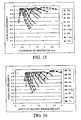
- FIG. 1shows a table of projected surface roughness induced loss associated with a range of roughness for the contrast and core size typical of a step contrast single mode erbium doped buried ridge wave guide amplifier (EDWA).
- EDWAerbium doped buried ridge wave guide amplifier
- FIG. 2shows deposition of material on a substrate to form a taper according to the present invention.
- FIG. 3shows an embodiment of a shadow mask that can be utilized to form a taper according to the present invention.
- FIG. 4shows thickness versus distance along a taper formed according to the present invention.
- FIG. 5shows the thickness versus distance for several tapers formed according to the present invention with different shadow mask geometries.
- FIGS. 6A and 6Bshow deposition of a taper according to the present invention and a cross-sectional diagram of a waveguide device, respectively.
- FIGS. 7A , 7 B, 7 C and 7 Dshow deposition of a taper according to the present invention and a cross-sectional diagram of waveguide devices, respectively.
- FIGS. 8A , 8 B and 8 Cshow another embodiment of a waveguide device with a taper according to the present invention.
- FIGS. 9A and 9Bshow another embodiment of a waveguide structure with a taper according to the present invention.
- FIG. 10shows the device illustrated in FIG. 6B utilized for coupling laser light into an optical fiber.
- FIG. 11shows the device illustrated in FIG. 7B utilized for coupling light into and out of two fibers.
- FIG. 12shows the device illustrated in FIG. 8B coupled to two optical fibers.
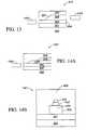
- FIG. 13shows the device illustrated in FIG. 8B coupled to an optical fiber and a laser.
- FIGS. 14A and 14Bshow a waveguide device according to the present invention with multiple tapered layers.
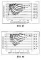
- FIG. 15shows the coupling efficiency of an embodiment of the device shown in FIG. 6B as a function of the thickness of the core for 1550 nm light.
- FIG. 16shows the coupling efficiency of a waveguide having a 2-D taper according to the present invention for 1550 nm light.
- FIG. 17shows the coupling efficiency at 980 nm for an embodiment of a taper as shown in FIG. 6 A.
- FIG. 18shows the coupling efficiency of an embodiment of a waveguide having a 2-D taper according to the present invention at 980 nm.
- RF sputtering of oxide filmsis discussed in application Ser. No. 09/903,050 (the '050 application) by Demaray et al., entitled “Planar Optical Devices and Methods for Their Manufacture,” assigned to the same assignee as is the present invention, herein incorporated by reference in its entirety.
- Depositions by biased pulse-DC sputteringare described in U.S. application Ser. No. 10/101,863 (the '863 application), herein incorporated by reference in its entirety.
- targets that can be utilized in a reactor according to the present inventionare discussed in U.S. application Ser. No.
- etched taperslimit the production of low loss wave guides with mode size transforming regions: sidewall and surface roughness, the terminal radius of the taper and most important, the relative fluctuation of the core dimension due to roughness for small core dimensions.
- a film with 5% thickness variationcan not be etched to the final 5% of the initial film thickness without becoming a discontinuous film, at least in parts.
- the same variationeither as a periodic structure or a terminal radius of an etched film can act as a scattering center, introducing unwanted loss or polarization to the guided light.
- the scattering loss induced by the roughness of the sides or top of the ridgeis increased by the high index contrast of the ridge to air.
- the claddingreduces the contrast to the core found in the air cladded ridge wave guide. Reduced contrast reduces the side wall scattering loss for wide width BCWs.
- the scattering loss due to roughnessis increased rapidly in at least two ways: First, scattering is increased in proportion to the contrast of the buried core with the cladding index; and Second, it is increased by the decrease in the size of the core that is required for single mode propagation at any wavelength with higher contrast.
- the scattering lossis proportional to the square of the ratio of the roughness dimension over the half width of the BCW core. This is known as the “relative fluctuation of the core thickness”. See FRANCOIS LADOUCCEUR, JOHN D. LOVE, SILICA-BASED BURIED CHANNEL WAVEGUIDES AND DEVICES, p. 98 (Chapman & Hall, 1996).
- a low refractive index contrast step BCW with a half width of 4.44 microns and a 0.2% contrastmust have a relative fluctuation of the core thickness of less than 1% to achieve a loss not greater than 0.01 dB/cm for light of 1.3 microns. Id.
- FIG. 1shows a table of the roughness induced loss associated with a range of roughness for the contrast and core size typical of a single mode BCW.
- the mode field diameterdecreases as the core half width decreases, demonstrating the dramatic concentration of the propagating light with increasing contrast and decreasing core size.
- the relative fluctuation of the core thickness and the loss in dB/cmare correlated for a range of roughness dimension from 0.001 to 0.256 microns (1 to 256 nm) in steps of 2 ⁇ .
- FIG. 1illustrates that the loss increases with surface roughness.
- the core half widths (half the size of the core width) chosen in FIG. 1are the largest values for which light at 980 nm, having the indicated mode field diameter, will be single mode at the tabulated index contrast.
- the loss that is correlated with the respective roughnessis an estimate for the loss in the range between 1.3 nm and 1.5 nm. This loss is representative of the scattering loss of a c band signal (i.e., a signal in the range 1528 to 1562 nm) co-propagating in the same wave guide with 980 nm pump light.
- the gain of a doped BCW amplifieris proportional to the number of dopant ions, for instance erbium ions, in the excited state.
- the fraction of excited active ionsis proportional to the intensity of the light. Consequently, it is of great utility to provide an adiabatic mode size transition from a small contrast, large mode wave guide, suitable for low loss coupling to fiber, to a high contrast, small mode wave guide.
- the mode field diameter in the range of between about 0.2% to 0.4%is similar to that of an SMF-28 fiber. Consequently a wave guide with this mode size will couple efficiently to light propagating from the fiber.
- such a wave guidecan have a side wall roughness between about 0.032 and about 0.064 microns for a loss of about 0.01 dB/cm. This is attainable for silica based materials by dry etching processes. However, this represents the lower limit of as etched sidewall roughness that can be achieved by lithography and dry etch for an eight to nine micron high etched sidewall.
- the intensity of the pump lightcould be increased very substantially.
- the mode field diameteris 2.4 microns.
- the increase in optical intensity of the pump lightis proportional to the square of the ratio of the respective mode field diameters which is approximately ⁇ (10/2.4) 2 ⁇ 17.
- FIG. 1clearly shows that the roughness required for a 6% contrast, 1 micron width wave guide is about 2 nm for the scattering loss to be less than about 0.01 dB/cm.
- the tabulated data shown in FIG. 1is an approximation, it is clear for higher index wave guides, tenths of nanometer or Angstrom roughness is required for low loss wave guide structures.
- the roughness of 1 micron high etched sidewallis difficult to reduce below about 0.032 microns.
- FIG. 1shows that the loss due to such a roughness is more than 3 dB/cm which is equivalent to the gain per centimeter of the very best erbium doped wave guide amplifiers, EDWAs.
- the roughness that governs the loss in a BCWis due to the mode limiting dimension of the core. That is, if the width is tapered to a smaller value, it is the roughness associated with, the side wall roughness associated with the relative variation in the width that determines the scattering loss. Likewise, if the thickness of the BCW is varied so as to limit the mode field of the guided light, it is the relative variation of the roughness associated with the thickness that is most important in governing the loss of the resulting BCW.
- taperingcan be achieved by etching using a gray scale mask techniques or a shadow mask. See, e.g., M. Itoh, et. al., “Large Reduction of Single Fiber Coupling Loss in 1.5% Delta Planar Lightwave Circuits using Spot-size Converters”, Electronic Letters 17 th Jan. 2002 Vol. 38 No. 2. Uniform etching of a film of tenths of microns to several microns over hundreds of microns of length is, however, very difficult. In particular the roughness of the surface of the core having the highest intensity of guided light is the most important. Re-melting can be used to smooth low temperature materials but not for materials that can not be raised to their melting point, for example erbium doped aluminasilicates.
- the thickness dimensionis often the smallest or mode limiting dimension.
- the roughness of the lateral edgesis of less importance since the mode size is confined proportionally more by the thickness dimension.
- dry etching of a surfaceis prone to roughness due to build up of non volatile components of the film as well as differential erosion due to density variation or differential etch selectivity of the component elements of the film.
- the use of an etch shadow maskis limited to a range of taper lengths due to the limited mean free path of the etching process.
- the mean free path in a gasis a measure of the average distance between collisions of the gas. It is also a measure of the line of sight distance a shadow can be projected in a gas.
- FIG. 2illustrates fabrication of a taper according to the present invention.
- Substrate 205is positioned opposite a target 204 in a PVD deposition chamber 200 .
- Powercan be applied to target 204 from power supply 201 such as is described in the '863 application and in the '050 application.
- bias powercan be applied to substrate 205 from bias power supply 202 .
- Sputtering gassescan be introduced to PVD chamber 200 .
- PVD chamber 200can be an RF sputtering chamber such as that described in the '050 application or a biased pulsed-DC sputtering chamber such as that described in the '863 application.
- a shadow mask 209is positioned over substrate 205 .
- mask 209may be fitted over a wafer substrate 205 .
- mask 209may be positioned on substrate 205 or be a structure previously formed on substrate 205 .
- Core film 206is then deposited, but with shadow mask 209 in place a smooth taper 207 is formed.
- the deposited film thickness decrease of taper 207can be achieved in a gradual, adiabatic taper rate over a distance of millimeters to several centimeters with high lateral taper uniformity.
- the surface roughness of the tapered filmcan be as good as about 0.2 nm or 2 Angstroms average roughness, providing an optical quality, low loss surface suitable for efficient mode transformation of high or low contrast structures and devices with very low scattering loss.
- FIG. 2shows a side view of shadow mask 209 in PVD deposition chamber 200 .
- Shadow mask 209is positioned above substrate 205 and adjacent to a region of substrate 205 which is to be coated with a core film 206 . Tapered portion 207 of layer 206 will result by the line of sight shadow provided by mask 209 .
- the vapor distribution from the sputter source of target 204is cosine like. That is, the intensity of the angular distribution of the atoms from target 204 goes to zero as the angle of departure of the sputtered atom from the surface of target 204 goes to zero. Sputtered vapor impinges on mask 209 and the region below mask 209 is substantially free of film.
- the region away from mask 209receives a flux of vapor from all directions, substantially independent of mask 209 .
- Vapor arriving at a surface of mask 209is collected on mask 209 .
- An upper surface of mask 209will project a shadow of collected material that will not arrive at the surface of substrate 205 , forming a tapered region 207 in layer 206 far from mask 209 . If the out of plane edge of mask 209 is a straight edge, and the distribution of incoming vapor is uniform, the taper of layer 206 will have a gradient that is perpendicular to the mask edge.
- FIG. 3shows the thickness profile for a deposition of about 1.8 microns thick, 0.8% Er/0.8% Yb doped (50/50)% aluminosilicate by PVD deposition using a reactive pulsed DC PVD process as described in the '863 application.
- the maskwas formed with a 100 mm square open region in a full coverage quartz disk that supported itself all around on table 203 , overlaying a 150 mm silicon wafer substrate 205 as shown in FIG. 2 .
- the resulting upper portion of shadow mask 209was approximately 0.5 mm thick, the underside was supported about 0.5 mm from the top surface of substrate 205 .
- the resulting film thickness taper 207 and surface roughness as measured by atomic force microscopy (AFM)is shown in FIG. 3 as a function of distance in mm.
- AFMatomic force microscopy
- the edge of the cutout of shadow mask 209was positioned approximately at the 25 mm position, above the position of film taper 207 at approximately half the full thickness of the film.
- Layer 206was deposited at a pulsed DC sputtering power of about 5 kWatts, at a rate of about 500 nm/hour, with substrate radio frequency power bias of about 300 Watts at 2 MHz.
- the filmhas an index contrast of about 4% to thermal oxide, as has been described in the '863 application.
- the first and last 10% of the film taper of taper region 207occurs over about 20 mm each.
- the remaining 80% of the taper in taper region 207occurs over about 10 mm or 10,000 microns. Consequently, over the steep portion of the film taper, the rate of taper in this example is about 1.400 microns/10,000 microns or 0.14 parts per thousand. Other embodiments will result in other geometries of taper region 207 .
- the surface roughness of the Er/Yb doped aluminosilicate film 206 of this example at the full thickness regionwas about 0.2 nm. A similar surface roughness was found at the half height region of the film taper 207 for this example.
- 3shows the maximum as-deposited roughness to be less than about 3 nm, which occurred in a region under shadow mask 209 .
- This roughnesswas interpreted as being due to weakly adherent film material which was subsequently removed from the surface of layer 206 by a cleaning processes to provide a surface roughness not greater than about 1 nm in this example.
- FIG. 4shows another embodiment of shadow mask 209 that was formed of quartz parts having a top piece 304 with a thickness T supported by a washer or spacer 302 with a thickness W on a base frame which was thicker by an amount D (e.g., about 0.3 nm) than substrate 205 .
- the taper 207can be a positive or negative taper in the thickness of layer 206 .
- the tapered filmcan be deposited over a planar film of the same composition without an interface between the two layers. In this way the taper can reduce the thickness of the combined film to a precisely determined continuing thickness, that of the initial film.
- This taper configurationcan be referred to as the YC taper.
- a region of no depositioncan be disposed under a shadow mask so that a positive taper is obtained on either side of mask 209 .
- mask 209can be utilized to form a well-like region in a layer of otherwise precise thickness.
- Mask 209 and substrate 205 to be coatedare introduced to a sputter target 204 having a substantially uniform area of target erosion as described in the '050 application and in the '863 application.
- a sputter targethas an area of erosion that is larger than the substrate to be coated.
- the sputter sourcecan be a planar magnetron but it should advantageously demonstrate an area of erosion adjacent to the article to be coated which is diode like in sputter erosion uniformity. It is preferred that such a sputter target sputter more than 20% of its weight as sputtered material before the non-uniformity of the film is more than about 10% of the film thickness and preferably as much as 50% of the target weight.
- Such a sputter sourceprovides a uniform distribution of sputtered vapor at substrate 205 .
- the sputter processshould have a mean free path at least as long as the length of tapered region 207 to be coated or longer.
- a sputter pressure of 1 milliTorris estimated to have a mean free path of about 10 cm. Consequently, a sputter pressure of 2 to 5 milliTorr will enable the mask to intercept vapor with a line of sight trajectory as far as several centimeters from the mask.
- a layer 206is deposited on the wafer having a film thickness which is smoothly increasing from zero thickness in the region under mask 209 to the region away from mask 209 which has a thickness similar to the thickness of layer 206 deposited with shadow mask 209 .
- the region of film having an increasing thickness, region 207is said to be in the line of sight shadow of the physical vapor.
- the formation of tapered thickness optical films by means of such a processlead directly to low loss, efficient mode size converting wave guides and amplifiers. See Tao Pan et al., “Gain Flattened, High Index Contrast Planar Er 3+ -doped Waveguide Amplifier with an Integrated Mode Size Converter,” submitted to Optical Fiber Conference, Mar. 19-21, Anneheim Ca., 2002.
- FIG. 4shows the height G which is the spacing of the under side of mask 209 to the top of substrate 206 . If this distance is more than about 1 mm, the substrate bias plasma, which is responsible for the densification and smoothing of the film, will be maintained under at least a portion of shadow mask 209 . This has the advantage of smoothing and providing optical transparency to the thin portion of the tapered film.
- mask 209can include a holder 208 with base frame 301 and mask support 303 .
- FIG. 5shows the taper profile for a series of depositions of varying gap and total height values for shadow deposition according to the present invention.
- FIGS. 6A and 6Billustrate an embodiment of a tapered waveguide structure according to the present invention.
- FIG. 6Ashows a waveguide structure 601 having core layer 206 deposited over a substrate 205 . Shadow mask 209 is positioned during deposition to form tapered region 207 .
- another layer 607is formed under core layer 206 .
- Layer 607can, for example, be an undercladding layer or another core (either active or passive) layer.
- substrate 205can be a silicon wafer which is thermally oxidized to form an undercladding layer 607 .
- waveguide 608is formed from deposited layer 206 by patterning layer 206 . Deposited layer 206 can be patterned by well known standard techniques.
- FIG. 6Bshows a cross section of a device 610 with core 608 formed from core layer 206 .
- An upper cladding layer 609is then formed over layer 607 and core 608 .
- Waveguide 608can be formed from a passive layer, an active layer, or a combination of active and passive layers.
- a passive core layercan, for example, be a layer of aluminasilicate material with no optically active dopants.
- An active layercan, for example, be a layer of rare-earth doped aluminasilicate material.
- erbium doped aluminasilicatecan be deposited as layer 206 and patterned to form an amplifying waveguide 608 . Depositions of passive layers, active layers and cladding layers of varying material properties has been described the '863 application, the '341 application and the '493 application.
- core 608may be formed from an active core material in layer 206 .
- Device 610can be an optical amplifier with mode-size converter coupling of light into and out of core 608 .
- Taper 207 in layer 206forms the mode-size converter.
- FIGS. 7A , 7 B and 7 Cillustrate another embodiment of tapered waveguide structures according to the present invention.
- structure 701includes tapered regions 207 formed on both sides of core layer 206 by shadow masks 209 . Therefore, when core layer 206 is patterned into waveguide 608 as shown in FIG. 7B , the resulting waveguide have tapered regions 207 on both sides.
- the cross-sectional view of device 710 formed from structure 701 in FIG. 7 BCore layer 206 is patterned to form waveguide 608 and upper cladding layer 609 is deposited over core layer 206 and undercladding layer 607 .
- Device 710can couple light into and out of both sides of waveguide 608 .
- core layer 206may be active core material and device 710 can function as an amplifier device.
- FIG. 7Cshows another waveguide device 720 .
- core layer 206is patterned.
- a core layer 604is then deposited and patterned to form core 608 .
- Upper cladding layer 609is then deposited over core 608 .
- core layer 206may be an active core layer and core layer 604 can be a passive core layer.
- Device 720then, can function as an amplifier.
- FIG. 7Dillustrates device 720 and a calculation of coupling efficiency in device 720 .
- the passive layer to active layer couplingi.e., layer 604 into layer 206
- the passive core to passive core lossis expected to be about 0.12 dB of modal loss.
- the index contrast between the active core and the claddingwas 7%.
- Passive core 604has a contrast of 0.5% with cladding layers.
- the taper lengthis about 1 mm.
- FIGS. 8A , 8 B and 8 Cshow another embodiment of a waveguide device with tapers according to the present invention.
- another core layer 604is deposited over undercladding layer 604 and core layer 206 is deposited according to the present invention over core layer 604 .
- Core layer 604can, for example, be an active or passive core layer.
- FIG. 8Bshows a cross-sectional view of waveguide device 810 .
- core layer 206is patterned and then core layer 604 is patterned to form core 608 .
- Uppercladding layer 609is then deposited over undercladding layer 607 and core 608 .
- core layer 604may be a passive core material and core layer 206 may be an active core material, for example erbium doped aluminasilicate, to form an amplifier structure.
- FIG. 8Cshows a cross-sectional view of waveguide device 820 .
- core layer 206is patterned and then core layer 604 is patterned.
- a second core layer 605is deposited over core layer 206 and patterned to form core 608 .
- Uppercladding layer 609is then deposited over core 608 .
- core layers 604 and 605are passive core layers and core layer 206 is an active core layer.
- Device 820then, can function as an amplifier.
- Coupling of light between a core of a core layer 604 and a core of core layer 206is determined by the index difference between core layer 604 and core layer 206 .
- Lightwill preferentially transition to the region of higher index. Therefore, in an active core region 206 of higher index over a passive core region 604 of lower index, light will transition from passive core region 604 to active core region 206 . If the vertical taper 207 of core layer 206 is long enough (for example greater than about 200 ⁇ m) and smooth enough, then the transition will be substantially adiabatic.
- FIGS. 9A and 9Bshow another embodiment of a waveguide structure with a taper according to the present invention.
- shadow mask 209is positioned such that tapered regions 207 are formed in the center of layer 206 .
- Layer 206can, in some embodiments, be deposited over another core layer 604 .
- Under cladding layer 607may be deposited between cladding layer 206 and substrate 205 .
- Structure 901can function as a waveguide converter to couple light into and out of two fibers formed in layer 206 .
- a light sourcemay be placed in the region between tapers 207 and light may be coupled into both sides of layer 206 .
- FIG. 9Bshows a cross-sectional view of a waveguide device 910 formed from structure 901 .
- Layer 206may be patterned and then layer 604 may be patterned to form a core 608 .
- layer 604may be absent and core 608 then includes only layer 206 .
- core 608may include another core layer deposited over layer 206 and patterned to form core 608 .
- Uppercladding layer 609is deposited over core 608 .
- Device 910as was discussed above, may be utilized to couple light from photodiodes or light to photodetectors that can be mounted in substrate 205 .
- FIG. 10shows device 1001 , which is an embodiment of device 610 shown in FIG. 6B , utilized to optically couple a laser 1003 with a fiber 1002 .
- Tapered region 207provides mode-size conversion for coupling light out of device 1001 into fiber 1002 efficiently.
- TP taperSuch a reverse taper mode size expander can be referred to as a “TP taper”.
- device 1001is polished such that layer 608 does not taper to zero.
- layer 608can have a high index of refraction so that the mode size of core 608 matches the mode size at the facet of laser 1003 and a high index contrast with cladding layers 607 and 609 such that the numerical aperature (NA) of laser 1003 and device 1001 can be closely matched, causing light from laser 1003 to be efficiently coupled into device 1001 .
- NAnumerical aperature
- FIG. 11shows device 710 as shown in FIG. 7B coupled to optical fibers 1102 and 1002 .
- Tapered regions 207 in both sides of device 710providing mode-size conversion which can be utilized to efficiently couple light between fiber 1002 and device 710 and between fiber 1102 and device 710 .
- device 710can function as an amplifier.
- FIG. 12shows device 810 as shown in FIG. 8B coupled to optical fibers 1102 and 1002 .
- tapered regions 207provide mode-size conversion which can efficiently couple light between fibers 1002 and 1102 and device 810 .
- device 810may be an amplifier device.
- layer 607can be a low index passive core.
- FIG. 13shows device 810 as shown in FIG. 8B having a single tapered region 207 coupled between laser 1003 and fiber 1002 .
- Laser 1003can be efficiently coupled into device 810 when core 608 formed of layers 206 and 604 is constructed such that the mode size of core 608 matches the mode size at the facet of laser 1003 and the numerical aperature (NA) of laser 1003 and device 610 can be closely matched.
- NAnumerical aperature
- FIGS. 14A and 14Billustrate an embodiment of a waveguide device having multiple tapered core layers.
- under cladding layer 607is formed on substrate 205 .
- a core layer 604can be deposited over under cladding layer 604 .
- Tapered core layer 1402is then deposited over core layer 604 .
- Tapered core layer 206is then deposited over tapered core layer 1402 .
- any number of tapered core layerscan be deposited.
- another core layermay be deposited over core layer 206 .
- Core layers 604 , 1402 and 206are then patterned to form core 608 .
- Upper cladding layer 609is then deposited over core layer 206 to form device 1401 .
- FIG. 14Bshows a cross section of device 1401 .
- core 608includes cores 604 , 1402 , and 206 .
- FIG. 15shows the coupling efficiency of an embodiment of device 610 shown in FIG. 6 B.
- Each curve in FIG. 15illustrates the projected coupling efficiency for a waveguide having a taper length of more than about 200 ⁇ m. Further, the calculation was done at a wavelength of 1550 nm.
- the mode in device 610depends on the wavelength of light and the index of the material of core 608 .
- each curveassumes a square, untapered, waveguide.
- the thickness of the thinnest portion of tapered region 207is then reduced and the coupling efficiency is calculated.
- Each individual curve in FIG. 15represents a calculation performed for a different value of index contrast between cladding layer 607 and core layer 206 , for example ⁇ n/n varying between about 1% and about 7%.
- FIG. 15shows that the coupling efficiency can be optimized for each index contrast with particular taper end-point thickness.
- FIG. 16shows a similar calculation for a waveguide structure such as device 610 which is also tapered in the plane of substrate 205 as well as out-of-plane taper region 207 .
- core 608is square. Again, the dimensions of core 608 can be optimized for efficient coupling of light with device 610 for particular dimensions for each curve. The calculation is also undertaken at 1550 nm, as was done in the calculations shown in FIG. 15 .
- FIG. 17shows the same calculation as was illustrated with FIG. 15 except for 980 nm light instead of for 1550 nm light.
- the coupling efficiency for 980 nm lightcan be optimized with tapered thickness.
- the optimized taper for 980 nm lightis not the same as the optimization projected for 1550 nm light.
- FIG. 18shows the same calculation as was illustrated with FIG. 16 except for 980 nm light instead of 1550 nm light. Again, the coupling efficiency for 980 nm light can be optimized with taper, but the optimization for 980 nm light is not the same as the optimization projected for 1550 nm light.
- a YC taperwas formed by reducing the thickness of a core layer 206 as is shown in FIG. 8 A.
- Layer 604is a thin layer of active core material with composition 1.5 cat. % erbium target deposited, for example, as described in the '863 application.
- Mask 209was positioned on the order of 0.5 mm above substrate 205 , resulting in a taper length of about 500 ⁇ m.
- Layer 206 having the same compositionis deposited over layer 604 .
- core 608is then formed from layers 604 and 206 .
- the indices of active core 608 cladding layers 607 and 609are 1.511 and 1.4565, respectively.
- the film thickness in mode expander region(i.e., the region where layer 206 has completely disappeared) is about 0.3 ⁇ m and the total thickness in the middle of waveguide is about 1 ⁇ m.
- the width of core 608is about 2.5 ⁇ m.
- the total insertion loss at 1310 nmwas measured to be only about 1.2 dB for 12 cm long waveguide, compared to 8 dB of insertion loss for about a 10 cm long waveguide without such a mode expander.
- FIGS. 8A and 8BIn another example of a mode size converter, as shown in FIGS. 8A and 8B , where layer 604 is a passive core layer and layer 206 is an active core layer with composition 1.0 cat. % of erbium deposited, for example, as described in the '050 application.
- Mask 209was configured as discussed above in the previous example.
- the index of refraction of passive core 604 relative to cladding layers 607 and 609is about 0.9%.
- the active core indexis about 1.508.
- the insertion loss at 1310 for 12 cm long waveguideis about 2 dB compared to 5 dB insertion loss for 7 cm long waveguide without the mode size converter.
- This double-core device coupleris a wide-band coupler for 980 nm as well as 1.5 ⁇ m light.
- Core 608is a high index core with high index contrast with cladding layers 607 and 609 .
- the high index passive core index and claddingare 1.55 and 1.4565, respectively, resulting in about a 6.4% contrast.
- the passive core 604has thickness of 0.5 micron and width of about 5 micron with 28 nm in length.
- the laser diodewas an ADC S/N 2412.
- the vertical and horizontal angular width (about 13% of the peak power) of this laser diodeis 65 degree and 11.6 degree, respectively.
- the coupling efficiency from this laser diode to waveguideis more than 65%.
- the present inventionalso relates to the integration of adiabatic mode size conversion in continuous waveguide structures having large change in index contrast. Utilizing the present invention, this coupling efficiency can be advantageously increased to between 80 and 90% between single laser die and single waveguides as well as arrays of laser dies and arrays of wavelengths.
- any combination of active and passive core layers with cladding layers of any relative dimensionscan be deposited.
- Any number of tapered core layerscan be utilized, having any index variation achievable.
- symmetrical claddingi.e., undercladding layer and uppercladding layers
- assymetric cladding layerscan also be utilized.
Landscapes
- Engineering & Computer Science (AREA)
- Physics & Mathematics (AREA)
- Chemical & Material Sciences (AREA)
- Microelectronics & Electronic Packaging (AREA)
- Optics & Photonics (AREA)
- General Physics & Mathematics (AREA)
- Materials Engineering (AREA)
- Organic Chemistry (AREA)
- Metallurgy (AREA)
- Mechanical Engineering (AREA)
- Chemical Kinetics & Catalysis (AREA)
- Power Engineering (AREA)
- Optical Integrated Circuits (AREA)
Abstract
Description
Claims (11)
Priority Applications (3)
| Application Number | Priority Date | Filing Date | Title |
|---|---|---|---|
| US10/101,492US6884327B2 (en) | 2002-03-16 | 2002-03-16 | Mode size converter for a planar waveguide |
| US11/100,856US8045832B2 (en) | 2002-03-16 | 2005-04-06 | Mode size converter for a planar waveguide |
| US11/100,864US20050183946A1 (en) | 2002-03-16 | 2005-04-06 | Mode size converter for a planar waveguide |
Applications Claiming Priority (1)
| Application Number | Priority Date | Filing Date | Title |
|---|---|---|---|
| US10/101,492US6884327B2 (en) | 2002-03-16 | 2002-03-16 | Mode size converter for a planar waveguide |
Related Child Applications (2)
| Application Number | Title | Priority Date | Filing Date |
|---|---|---|---|
| US11/100,864ContinuationUS20050183946A1 (en) | 2002-03-16 | 2005-04-06 | Mode size converter for a planar waveguide |
| US11/100,856DivisionUS8045832B2 (en) | 2002-03-16 | 2005-04-06 | Mode size converter for a planar waveguide |
Publications (2)
| Publication Number | Publication Date |
|---|---|
| US20030173208A1 US20030173208A1 (en) | 2003-09-18 |
| US6884327B2true US6884327B2 (en) | 2005-04-26 |
Family
ID=28040015
Family Applications (3)
| Application Number | Title | Priority Date | Filing Date |
|---|---|---|---|
| US10/101,492Expired - LifetimeUS6884327B2 (en) | 2002-03-16 | 2002-03-16 | Mode size converter for a planar waveguide |
| US11/100,856Expired - Fee RelatedUS8045832B2 (en) | 2002-03-16 | 2005-04-06 | Mode size converter for a planar waveguide |
| US11/100,864AbandonedUS20050183946A1 (en) | 2002-03-16 | 2005-04-06 | Mode size converter for a planar waveguide |
Family Applications After (2)
| Application Number | Title | Priority Date | Filing Date |
|---|---|---|---|
| US11/100,856Expired - Fee RelatedUS8045832B2 (en) | 2002-03-16 | 2005-04-06 | Mode size converter for a planar waveguide |
| US11/100,864AbandonedUS20050183946A1 (en) | 2002-03-16 | 2005-04-06 | Mode size converter for a planar waveguide |
Country Status (1)
| Country | Link |
|---|---|
| US (3) | US6884327B2 (en) |
Cited By (43)
| Publication number | Priority date | Publication date | Assignee | Title |
|---|---|---|---|---|
| US20030063883A1 (en)* | 2001-07-10 | 2003-04-03 | Demaray Richard E. | As-deposited planar optical waveguides with low scattering loss and methods for their manufacture |
| US20030134054A1 (en)* | 2001-11-09 | 2003-07-17 | Demaray Richard E. | Low temperature zirconia based thermal barrier layer by PVD |
| US20030175142A1 (en)* | 2002-03-16 | 2003-09-18 | Vassiliki Milonopoulou | Rare-earth pre-alloyed PVD targets for dielectric planar applications |
| US20030173207A1 (en)* | 2002-03-16 | 2003-09-18 | Symmorphix, Inc. | Biased pulse DC reactive sputtering of oxide films |
| US20040105644A1 (en)* | 2002-08-27 | 2004-06-03 | David Dawes | Optically coupling into highly uniform waveguides |
| US20040259305A1 (en)* | 2003-05-23 | 2004-12-23 | Demaray Richard E. | Energy conversion and storage films and devices by physical vapor deposition of titanium and titanium oxides and sub-oxides |
| US20040264905A1 (en)* | 2003-04-29 | 2004-12-30 | Blauvelt Henry A. | Multiple-core planar optical waveguides and methods of fabrication and use thereof |
| US20050006768A1 (en)* | 2003-02-27 | 2005-01-13 | Mukundan Narasimhan | Dielectric barrier layer films |
| US20050175287A1 (en)* | 2002-03-16 | 2005-08-11 | Tao Pan | Mode size converter for a planar waveguide |
| US20090154880A1 (en)* | 2007-12-12 | 2009-06-18 | Electronics And Telecommunications Research Institute | Photonics device |
| US20090162013A1 (en)* | 2007-12-12 | 2009-06-25 | Lightwire, Inc. | Coupling between free space and optical waveguide using etched coupling surfaces |
| US20100003167A1 (en)* | 2006-10-30 | 2010-01-07 | Stc.Unm | Magnetically susceptible particles and apparatuses for mixing the same |
| US7646957B2 (en) | 2005-02-15 | 2010-01-12 | Hoya Corporation Usa | Multiple-core planar optical waveguides and methods of fabrication and use thereof |
| US20100304514A1 (en)* | 2003-04-22 | 2010-12-02 | Block Bruce A | Efficient light coupler from off-chip to on-chip waveguides |
| US7959769B2 (en) | 2004-12-08 | 2011-06-14 | Infinite Power Solutions, Inc. | Deposition of LiCoO2 |
| US7993773B2 (en) | 2002-08-09 | 2011-08-09 | Infinite Power Solutions, Inc. | Electrochemical apparatus with barrier layer protected substrate |
| US8021778B2 (en) | 2002-08-09 | 2011-09-20 | Infinite Power Solutions, Inc. | Electrochemical apparatus with barrier layer protected substrate |
| US8062708B2 (en) | 2006-09-29 | 2011-11-22 | Infinite Power Solutions, Inc. | Masking of and material constraint for depositing battery layers on flexible substrates |
| US8197781B2 (en) | 2006-11-07 | 2012-06-12 | Infinite Power Solutions, Inc. | Sputtering target of Li3PO4 and method for producing same |
| US8236443B2 (en) | 2002-08-09 | 2012-08-07 | Infinite Power Solutions, Inc. | Metal film encapsulation |
| US8260203B2 (en) | 2008-09-12 | 2012-09-04 | Infinite Power Solutions, Inc. | Energy device with integral conductive surface for data communication via electromagnetic energy and method thereof |
| US8268488B2 (en) | 2007-12-21 | 2012-09-18 | Infinite Power Solutions, Inc. | Thin film electrolyte for thin film batteries |
| US8350519B2 (en) | 2008-04-02 | 2013-01-08 | Infinite Power Solutions, Inc | Passive over/under voltage control and protection for energy storage devices associated with energy harvesting |
| US8394522B2 (en) | 2002-08-09 | 2013-03-12 | Infinite Power Solutions, Inc. | Robust metal film encapsulation |
| US8404376B2 (en) | 2002-08-09 | 2013-03-26 | Infinite Power Solutions, Inc. | Metal film encapsulation |
| US8431264B2 (en) | 2002-08-09 | 2013-04-30 | Infinite Power Solutions, Inc. | Hybrid thin-film battery |
| US8445130B2 (en) | 2002-08-09 | 2013-05-21 | Infinite Power Solutions, Inc. | Hybrid thin-film battery |
| US8508193B2 (en) | 2008-10-08 | 2013-08-13 | Infinite Power Solutions, Inc. | Environmentally-powered wireless sensor module |
| US8518581B2 (en) | 2008-01-11 | 2013-08-27 | Inifinite Power Solutions, Inc. | Thin film encapsulation for thin film batteries and other devices |
| US8599572B2 (en) | 2009-09-01 | 2013-12-03 | Infinite Power Solutions, Inc. | Printed circuit board with integrated thin film battery |
| US8636876B2 (en) | 2004-12-08 | 2014-01-28 | R. Ernest Demaray | Deposition of LiCoO2 |
| US8728285B2 (en) | 2003-05-23 | 2014-05-20 | Demaray, Llc | Transparent conductive oxides |
| US8906523B2 (en) | 2008-08-11 | 2014-12-09 | Infinite Power Solutions, Inc. | Energy device with integral collector surface for electromagnetic energy harvesting and method thereof |
| US9325140B2 (en) | 2013-03-14 | 2016-04-26 | Massachusetts Institute Of Technology | Photonic devices and methods of using and making photonic devices |
| US9334557B2 (en) | 2007-12-21 | 2016-05-10 | Sapurast Research Llc | Method for sputter targets for electrolyte films |
| US9366816B2 (en) | 2012-11-12 | 2016-06-14 | Demaray, Llc | Adiabatic planar waveguide coupler transformer |
| US20160246010A1 (en)* | 2015-02-20 | 2016-08-25 | Si-Ware Systems | Selective step coverage for micro-fabricated structures |
| US9435950B2 (en)* | 2014-07-24 | 2016-09-06 | Sumitomo Electric Industries, Ltd. | Semiconductor optical device |
| US9634296B2 (en) | 2002-08-09 | 2017-04-25 | Sapurast Research Llc | Thin film battery on an integrated circuit or circuit board and method thereof |
| US10680277B2 (en) | 2010-06-07 | 2020-06-09 | Sapurast Research Llc | Rechargeable, high-density electrochemical device |
| US10818909B2 (en) | 2016-05-09 | 2020-10-27 | Demaray, Llc | Energy storage device with a first metal layer formed from a precursor layer upon charge and diffused into a cathode during discharge |
| US20220214498A1 (en)* | 2019-04-24 | 2022-07-07 | University Of Southampton | Photonic chip and method of manufacture |
| US11808997B1 (en)* | 2022-09-19 | 2023-11-07 | Nexus Photonics Inc. | Heterogeneous photonic integrated circuits with doped waveguides |
Families Citing this family (16)
| Publication number | Priority date | Publication date | Assignee | Title |
|---|---|---|---|---|
| US7142759B2 (en)* | 2004-01-13 | 2006-11-28 | Lionix Bv | Surface waveguide and method of manufacture |
| US7838133B2 (en) | 2005-09-02 | 2010-11-23 | Springworks, Llc | Deposition of perovskite and other compound ceramic films for dielectric applications |
| US8170383B2 (en)* | 2006-12-01 | 2012-05-01 | Nec Corporation | Optical converter |
| US8483528B2 (en)* | 2008-02-29 | 2013-07-09 | Google Inc. | Optical mode transformer, in particular for coupling an optical fiber and a high-index contrast waveguide |
| US9040919B2 (en)* | 2010-10-25 | 2015-05-26 | Thomas E. Darcie | Photomixer-waveguide coupling tapers |
| US9182544B2 (en)* | 2011-12-21 | 2015-11-10 | Intel Corporation | Fabrication of planar light-wave circuits (PLCS) for optical I/O |
| JP5865145B2 (en)* | 2012-03-19 | 2016-02-17 | リコー光学株式会社 | Concave micropattern forming method and concave micropattern substrate |
| US9311935B2 (en)* | 2013-11-07 | 2016-04-12 | HGST Netherlands B.V. | Method and apparatus for magnetic recording head having a waveguide |
| US8908482B1 (en)* | 2014-02-14 | 2014-12-09 | HGST Netherlands B.V. | Sacrificial protection layer for preventing ion mill damage to HAMR optical components |
| US9202493B1 (en) | 2014-02-28 | 2015-12-01 | Western Digital (Fremont), Llc | Method of making an ultra-sharp tip mode converter for a HAMR head |
| US9310555B2 (en) | 2014-05-16 | 2016-04-12 | Tyco Electronics Corporation | Mode size converters and methods of fabricating the same |
| EP3153899B1 (en) | 2015-10-09 | 2024-07-31 | Huawei Technologies Research & Development Belgium NV | Optical coupling scheme |
| CN110699671B (en)* | 2019-10-21 | 2022-05-20 | 江苏菲沃泰纳米科技股份有限公司 | Coating fixture and its application |
| CN110699662B (en)* | 2019-10-21 | 2022-05-27 | 江苏菲沃泰纳米科技股份有限公司 | Film coating method and film layer thereof |
| WO2021078151A1 (en) | 2019-10-21 | 2021-04-29 | 江苏菲沃泰纳米科技有限公司 | Coating method and film layer thereof, and coating fixture and application thereof |
| US11921325B2 (en)* | 2020-02-27 | 2024-03-05 | Taiwan Semiconductor Manufacturing Company Limited | Semiconductor device and method of making |
Citations (10)
| Publication number | Priority date | Publication date | Assignee | Title |
|---|---|---|---|---|
| US5107538A (en) | 1991-06-06 | 1992-04-21 | At&T Bell Laboratories | Optical waveguide system comprising a rare-earth Si-based optical device |
| US5119460A (en) | 1991-04-25 | 1992-06-02 | At&T Bell Laboratories | Erbium-doped planar optical device |
| US5206925A (en)* | 1990-06-29 | 1993-04-27 | Hitachi Cable Limited | Rare earth element-doped optical waveguide and process for producing the same |
| US5381262A (en) | 1992-08-18 | 1995-01-10 | Fujitsu Limited | Planar wave guide type optical amplifier |
| US5457569A (en)* | 1994-06-30 | 1995-10-10 | At&T Ipm Corp. | Semiconductor amplifier or laser having integrated lens |
| US5563979A (en) | 1995-08-31 | 1996-10-08 | Lucent Technologies Inc. | Erbium-doped planar optical device |
| US5613995A (en) | 1993-04-23 | 1997-03-25 | Lucent Technologies Inc. | Method for making planar optical waveguides |
| US5900057A (en) | 1995-01-17 | 1999-05-04 | Lucent Technologies Inc. | Planar waveguide and a process for its fabrication |
| US6058233A (en)* | 1998-06-30 | 2000-05-02 | Lucent Technologies Inc. | Waveguide array with improved efficiency for wavelength routers and star couplers in integrated optics |
| US6290821B1 (en)* | 1999-07-15 | 2001-09-18 | Seagate Technology Llc | Sputter deposition utilizing pulsed cathode and substrate bias power |
Family Cites Families (222)
| Publication number | Priority date | Publication date | Assignee | Title |
|---|---|---|---|---|
| US3309302A (en) | 1963-10-07 | 1967-03-14 | Varian Associates | Method of preparing an electron tube including sputtering a suboxide of titanium on dielectric components thereof |
| US3616403A (en) | 1968-10-25 | 1971-10-26 | Ibm | Prevention of inversion of p-type semiconductor material during rf sputtering of quartz |
| US3850604A (en) | 1972-12-11 | 1974-11-26 | Gte Laboratories Inc | Preparation of chalcogenide glass sputtering targets |
| US4111523A (en) | 1973-07-23 | 1978-09-05 | Bell Telephone Laboratories, Incorporated | Thin film optical waveguide |
| US4082569A (en) | 1977-02-22 | 1978-04-04 | The United States Of America As Represented By The Administrator Of The National Aeronautics And Space Administration | Solar cell collector |
| US4437966A (en) | 1982-09-30 | 1984-03-20 | Gte Products Corporation | Sputtering cathode apparatus |
| DE3345659A1 (en) | 1983-06-16 | 1984-12-20 | Max-Planck-Gesellschaft zur Förderung der Wissenschaften e.V., 3400 Göttingen | ZIRCONIUM DIOXIDE CERAMIC BODY (ZRO (DOWN ARROW) 2 (DOWN ARROW)) AND METHOD FOR PRODUCING THE SAME |
| EP0140638B1 (en) | 1983-10-17 | 1988-06-29 | Tosoh Corporation | High-strength zirconia type sintered body and process for preparation thereof |
| DE3417732A1 (en) | 1984-05-12 | 1986-07-10 | Leybold-Heraeus GmbH, 5000 Köln | METHOD FOR APPLYING SILICON-CONTAINING LAYERS TO SUBSTRATES BY CATODIZING AND SPRAYING CATODE FOR CARRYING OUT THE METHOD |
| GB8414878D0 (en) | 1984-06-11 | 1984-07-18 | Gen Electric Co Plc | Integrated optical waveguides |
| US4785459A (en)* | 1985-05-01 | 1988-11-15 | Baer Thomas M | High efficiency mode matched solid state laser with transverse pumping |
| KR910000273B1 (en) | 1985-05-09 | 1991-01-23 | 마쯔시다덴기산교 가부시기가이샤 | Plasma processor |
| US4710940A (en) | 1985-10-01 | 1987-12-01 | California Institute Of Technology | Method and apparatus for efficient operation of optically pumped laser |
| US5173271A (en) | 1985-12-04 | 1992-12-22 | Massachusetts Institute Of Technology | Enhanced radiative zone-melting recrystallization method and apparatus |
| US5296089A (en) | 1985-12-04 | 1994-03-22 | Massachusetts Institute Of Technology | Enhanced radiative zone-melting recrystallization method and apparatus |
| DE3738738C1 (en) | 1987-11-14 | 1989-01-26 | Degussa | Powder-metallurgical process for producing targets |
| US4915810A (en) | 1988-04-25 | 1990-04-10 | Unisys Corporation | Target source for ion beam sputter deposition |
| JP2501118B2 (en) | 1988-06-17 | 1996-05-29 | 忠弘 大見 | Method for manufacturing semiconductor device |
| US5792550A (en) | 1989-10-24 | 1998-08-11 | Flex Products, Inc. | Barrier film having high colorless transparency and method |
| JP2758948B2 (en) | 1989-12-15 | 1998-05-28 | キヤノン株式会社 | Thin film formation method |
| DE4022090A1 (en)* | 1989-12-18 | 1991-06-20 | Forschungszentrum Juelich Gmbh | ELECTRO-OPTICAL COMPONENT AND METHOD FOR THE PRODUCTION THEREOF |
| US5252194A (en) | 1990-01-26 | 1993-10-12 | Varian Associates, Inc. | Rotating sputtering apparatus for selected erosion |
| US5085904A (en) | 1990-04-20 | 1992-02-04 | E. I. Du Pont De Nemours And Company | Barrier materials useful for packaging |
| US5306569A (en) | 1990-06-15 | 1994-04-26 | Hitachi Metals, Ltd. | Titanium-tungsten target material and manufacturing method thereof |
| US5645626A (en) | 1990-08-10 | 1997-07-08 | Bend Research, Inc. | Composite hydrogen separation element and module |
| US5225288A (en) | 1990-08-10 | 1993-07-06 | E. I. Du Pont De Nemours And Company | Solvent blockers and multilayer barrier coatings for thin films |
| US5078516A (en)* | 1990-11-06 | 1992-01-07 | Bell Communications Research, Inc. | Tapered rib waveguides |
| NL9002844A (en) | 1990-12-21 | 1992-07-16 | Philips Nv | SYSTEM INCLUDING A DEVICE AND A CASSETTE, AND A DEVICE AND A CASSETTE SUITABLE FOR USE IN SUCH A SYSTEM. |
| US5200029A (en) | 1991-04-25 | 1993-04-06 | At&T Bell Laboratories | Method of making a planar optical amplifier |
| US5196041A (en)* | 1991-09-17 | 1993-03-23 | The Charles Stark Draper Laboratory, Inc. | Method of forming an optical channel waveguide by gettering |
| US5355089A (en) | 1992-07-22 | 1994-10-11 | Duracell Inc. | Moisture barrier for battery with electrochemical tester |
| JP2755844B2 (en) | 1991-09-30 | 1998-05-25 | シャープ株式会社 | Plastic substrate liquid crystal display |
| US5702829A (en) | 1991-10-14 | 1997-12-30 | Commissariat A L'energie Atomique | Multilayer material, anti-erosion and anti-abrasion coating incorporating said multilayer material |
| ES2103030T3 (en) | 1991-12-11 | 1997-08-16 | Mobil Oil Corp | HIGH QUALITY BARRIER FILM. |
| US5287427A (en) | 1992-05-05 | 1994-02-15 | At&T Bell Laboratories | Method of making an article comprising an optical component, and article comprising the component |
| US5338625A (en) | 1992-07-29 | 1994-08-16 | Martin Marietta Energy Systems, Inc. | Thin film battery and method for making same |
| US5538796A (en) | 1992-10-13 | 1996-07-23 | General Electric Company | Thermal barrier coating system having no bond coat |
| JP3231900B2 (en) | 1992-10-28 | 2001-11-26 | 株式会社アルバック | Film forming equipment |
| US5942089A (en) | 1996-04-22 | 1999-08-24 | Northwestern University | Method for sputtering compounds on a substrate |
| US5789071A (en) | 1992-11-09 | 1998-08-04 | Northwestern University | Multilayer oxide coatings |
| JPH06158308A (en) | 1992-11-24 | 1994-06-07 | Hitachi Metals Ltd | Target for sputtering for indium-tin oxide film and its production |
| US6022458A (en) | 1992-12-07 | 2000-02-08 | Canon Kabushiki Kaisha | Method of production of a semiconductor substrate |
| AU669754B2 (en) | 1992-12-18 | 1996-06-20 | Becton Dickinson & Company | Barrier coating |
| US5303319A (en) | 1992-12-28 | 1994-04-12 | Honeywell Inc. | Ion-beam deposited multilayer waveguides and resonators |
| US5427669A (en) | 1992-12-30 | 1995-06-27 | Advanced Energy Industries, Inc. | Thin film DC plasma processing system |
| US5718813A (en) | 1992-12-30 | 1998-02-17 | Advanced Energy Industries, Inc. | Enhanced reactive DC sputtering system |
| JPH06279185A (en) | 1993-03-25 | 1994-10-04 | Canon Inc | Forming method of diamond crystal and diamond crystal film |
| SG46607A1 (en) | 1993-07-28 | 1998-02-20 | Asahi Glass Co Ltd | Method of an apparatus for sputtering |
| US5499207A (en) | 1993-08-06 | 1996-03-12 | Hitachi, Ltd. | Semiconductor memory device having improved isolation between electrodes, and process for fabricating the same |
| JP2642849B2 (en) | 1993-08-24 | 1997-08-20 | 株式会社フロンテック | Thin film manufacturing method and manufacturing apparatus |
| US5478456A (en) | 1993-10-01 | 1995-12-26 | Minnesota Mining And Manufacturing Company | Sputtering target |
| EP0652308B1 (en) | 1993-10-14 | 2002-03-27 | Neuralsystems Corporation | Method of and apparatus for forming single-crystalline thin film |
| US5738731A (en) | 1993-11-19 | 1998-04-14 | Mega Chips Corporation | Photovoltaic device |
| US5433835B1 (en) | 1993-11-24 | 1997-05-20 | Applied Materials Inc | Sputtering device and target with cover to hold cooling fluid |
| US5487822A (en) | 1993-11-24 | 1996-01-30 | Applied Materials, Inc. | Integrated sputtering target assembly |
| US5654984A (en) | 1993-12-03 | 1997-08-05 | Silicon Systems, Inc. | Signal modulation across capacitors |
| US5569520A (en) | 1994-01-12 | 1996-10-29 | Martin Marietta Energy Systems, Inc. | Rechargeable lithium battery for use in applications requiring a low to high power output |
| US5561004A (en) | 1994-02-25 | 1996-10-01 | Bates; John B. | Packaging material for thin film lithium batteries |
| US5475528A (en) | 1994-03-25 | 1995-12-12 | Corning Incorporated | Optical signal amplifier glasses |
| US5472795A (en) | 1994-06-27 | 1995-12-05 | Board Of Regents Of The University Of The University Of Wisconsin System, On Behalf Of The University Of Wisconsin-Milwaukee | Multilayer nanolaminates containing polycrystalline zirconia |
| WO1996000996A1 (en) | 1994-06-30 | 1996-01-11 | The Whitaker Corporation | Planar hybrid optical amplifier |
| JP3407409B2 (en) | 1994-07-27 | 2003-05-19 | 富士通株式会社 | Manufacturing method of high dielectric constant thin film |
| US5483613A (en) | 1994-08-16 | 1996-01-09 | At&T Corp. | Optical device with substrate and waveguide structure having thermal matching interfaces |
| US5909346A (en) | 1994-08-26 | 1999-06-01 | Aiwa Research & Development, Inc. | Thin magnetic film including multiple geometry gap structures on a common substrate |
| US6204111B1 (en) | 1994-12-28 | 2001-03-20 | Matsushita Electronics Corporation | Fabrication method of capacitor for integrated circuit |
| CN1075243C (en) | 1994-12-28 | 2001-11-21 | 松下电器产业株式会社 | Capacitance element for integrated circuit and manufacturing method thereof |
| US5607789A (en) | 1995-01-23 | 1997-03-04 | Duracell Inc. | Light transparent multilayer moisture barrier for electrochemical cell tester and cell employing same |
| JP3804974B2 (en) | 1995-01-25 | 2006-08-02 | アプライド コマツ テクノロジー株式会社 | Autoclave bonding of sputtering target assemblies |
| US6444750B1 (en) | 1995-03-06 | 2002-09-03 | Exxonmobil Oil Corp. | PVOH-based coating solutions |
| AUPN258095A0 (en) | 1995-04-21 | 1995-05-18 | Unisearch Limited | Low temperature fabrication of silica-based pecvd channel waveguides |
| US5771562A (en) | 1995-05-02 | 1998-06-30 | Motorola, Inc. | Passivation of organic devices |
| WO1996036746A1 (en) | 1995-05-18 | 1996-11-21 | Asahi Glass Company Ltd. | Process for producing sputtering target |
| KR100342189B1 (en) | 1995-07-12 | 2002-11-30 | 삼성전자 주식회사 | Method for producing rare earth elements-added optical fiber by using volatile composite |
| EP0761838B1 (en) | 1995-08-18 | 2001-08-08 | W.C. Heraeus GmbH & Co. KG | Sputtering target and method for its manufacturing |
| US5689522A (en) | 1995-10-02 | 1997-11-18 | The Regents Of The University Of California | High efficiency 2 micrometer laser utilizing wing-pumped Tm3+ and a laser diode array end-pumping architecture |
| US5719976A (en) | 1995-10-24 | 1998-02-17 | Lucent Technologies, Inc. | Optimized waveguide structure |
| JP3298799B2 (en) | 1995-11-22 | 2002-07-08 | ルーセント テクノロジーズ インコーポレイテッド | Cladding pump fiber and its manufacturing method |
| US5686360A (en) | 1995-11-30 | 1997-11-11 | Motorola | Passivation of organic devices |
| US5811177A (en) | 1995-11-30 | 1998-09-22 | Motorola, Inc. | Passivation of electroluminescent organic devices |
| US5955161A (en) | 1996-01-30 | 1999-09-21 | Becton Dickinson And Company | Blood collection tube assembly |
| US5972516A (en) | 1996-02-29 | 1999-10-26 | Kyocera Corporation | Method for manufacturing optical waveguide using siloxane polymer, and optoelectronic hybrid substrate using the optical waveguide |
| WO1997035044A1 (en) | 1996-03-22 | 1997-09-25 | Materials Research Corporation | Method and apparatus for rf diode sputtering |
| US5930584A (en) | 1996-04-10 | 1999-07-27 | United Microelectronics Corp. | Process for fabricating low leakage current electrode for LPCVD titanium oxide films |
| JPH1010675A (en) | 1996-04-22 | 1998-01-16 | Fuji Photo Film Co Ltd | Recording material |
| JP3346167B2 (en) | 1996-05-27 | 2002-11-18 | 三菱マテリアル株式会社 | High-strength dielectric sputtering target, method for producing the same, and film |
| WO1997047695A1 (en) | 1996-06-12 | 1997-12-18 | Hoechst Trespaphan Gmbh | Transparent barrier coatings exhibiting reduced thin film interference |
| US5761234A (en) | 1996-07-09 | 1998-06-02 | Sdl, Inc. | High power, reliable optical fiber pumping system with high redundancy for use in lightwave communication systems |
| US5731661A (en) | 1996-07-15 | 1998-03-24 | Motorola, Inc. | Passivation of electroluminescent organic devices |
| US5855744A (en) | 1996-07-19 | 1999-01-05 | Applied Komatsu Technology, Inc. | Non-planar magnet tracking during magnetron sputtering |
| US5693956A (en) | 1996-07-29 | 1997-12-02 | Motorola | Inverted oleds on hard plastic substrate |
| JP3631341B2 (en) | 1996-10-18 | 2005-03-23 | Tdk株式会社 | Multilayer composite functional element and method for manufacturing the same |
| US5841931A (en)* | 1996-11-26 | 1998-11-24 | Massachusetts Institute Of Technology | Methods of forming polycrystalline semiconductor waveguides for optoelectronic integrated circuits, and devices formed thereby |
| GB9625231D0 (en)* | 1996-12-04 | 1997-01-22 | Univ Southampton | Optical amplifiers & lasers |
| US6144795A (en)* | 1996-12-13 | 2000-11-07 | Corning Incorporated | Hybrid organic-inorganic planar optical waveguide device |
| UA47454C2 (en)* | 1996-12-20 | 2002-07-15 | Научний Центр Волоконной Оптікі Прі Інстітутє Общєй Фізікі Россійской Акадєміі Наук | Fiber converter of the mode field diameter, method for local chanche of the refractive index of the optical waveguides and a method for preparing raw stock for optical waveguides |
| JPH10195649A (en) | 1996-12-27 | 1998-07-28 | Sony Corp | Magnetron sputtering apparatus and method of manufacturing semiconductor device |
| US5944964A (en) | 1997-02-13 | 1999-08-31 | Optical Coating Laboratory, Inc. | Methods and apparatus for preparing low net stress multilayer thin film coatings |
| JPH10229201A (en) | 1997-02-14 | 1998-08-25 | Sony Corp | Manufacture of thin-film semiconductor device |
| US5847865A (en)* | 1997-02-18 | 1998-12-08 | Regents Of The University Of Minnesota | Waveguide optical amplifier |
| JP3098204B2 (en)* | 1997-03-07 | 2000-10-16 | ティーディーケイ株式会社 | Alloy target for magneto-optical recording, its manufacturing method and its reproducing method |
| US5952778A (en) | 1997-03-18 | 1999-09-14 | International Business Machines Corporation | Encapsulated organic light emitting device |
| JPH10265948A (en) | 1997-03-25 | 1998-10-06 | Rohm Co Ltd | Substrate for semiconductor device and method of manufacturing the same |
| EP0867985B1 (en) | 1997-03-27 | 2001-02-14 | Nederlandse Organisatie Voor Toegepast-Natuurwetenschappelijk Onderzoek Tno | Erbium-doped planar waveguide |
| US6106933A (en) | 1997-04-03 | 2000-08-22 | Toray Industries, Inc. | Transparent gas barrier biaxially oriented polypropylene film, a laminate film, and a production method thereof |
| US6242132B1 (en) | 1997-04-16 | 2001-06-05 | Ut-Battelle, Llc | Silicon-tin oxynitride glassy composition and use as anode for lithium-ion battery |
| US5948215A (en) | 1997-04-21 | 1999-09-07 | Tokyo Electron Limited | Method and apparatus for ionized sputtering |
| JP3290375B2 (en) | 1997-05-12 | 2002-06-10 | 松下電器産業株式会社 | Organic electroluminescent device |
| US5830330A (en) | 1997-05-22 | 1998-11-03 | Tokyo Electron Limited | Method and apparatus for low pressure sputtering |
| US6000603A (en) | 1997-05-23 | 1999-12-14 | 3M Innovative Properties Company | Patterned array of metal balls and methods of making |
| US5977582A (en) | 1997-05-23 | 1999-11-02 | Lucent Technologies Inc. | Capacitor comprising improved TaOx -based dielectric |
| US6051114A (en) | 1997-06-23 | 2000-04-18 | Applied Materials, Inc. | Use of pulsed-DC wafer bias for filling vias/trenches with metal in HDP physical vapor deposition |
| US5831262A (en) | 1997-06-27 | 1998-11-03 | Lucent Technologies Inc. | Article comprising an optical fiber attached to a micromechanical device |
| JP3813740B2 (en) | 1997-07-11 | 2006-08-23 | Tdk株式会社 | Substrates for electronic devices |
| US6041734A (en) | 1997-12-01 | 2000-03-28 | Applied Materials, Inc. | Use of an asymmetric waveform to control ion bombardment during substrate processing |
| US6052397A (en)* | 1997-12-05 | 2000-04-18 | Sdl, Inc. | Laser diode device having a substantially circular light output beam and a method of forming a tapered section in a semiconductor device to provide for a reproducible mode profile of the output beam |
| US5976327A (en) | 1997-12-12 | 1999-11-02 | Applied Materials, Inc. | Step coverage and overhang improvement by pedestal bias voltage modulation |
| US6004660A (en) | 1998-03-12 | 1999-12-21 | E.I. Du Pont De Nemours And Company | Oxygen barrier composite film structure |
| US6563998B1 (en) | 1999-04-15 | 2003-05-13 | John Farah | Polished polymide substrate |
| US20020014406A1 (en) | 1998-05-21 | 2002-02-07 | Hiroshi Takashima | Aluminum target material for sputtering and method for producing same |
| EP0960955A1 (en) | 1998-05-26 | 1999-12-01 | Universiteit Gent | Method and apparatus for flame spraying to form a tough coating |
| JP3126698B2 (en) | 1998-06-02 | 2001-01-22 | 富士通株式会社 | Sputter film forming method, sputter film forming apparatus, and semiconductor device manufacturing method |
| US6093944A (en) | 1998-06-04 | 2000-07-25 | Lucent Technologies Inc. | Dielectric materials of amorphous compositions of TI-O2 doped with rare earth elements and devices employing same |
| KR100287176B1 (en) | 1998-06-25 | 2001-04-16 | 윤종용 | Method for forming a capacitor using high temperature oxidation |
| DE19831719A1 (en)* | 1998-07-15 | 2000-01-20 | Alcatel Sa | Process for the production of planar waveguide structures and waveguide structure |
| US6358810B1 (en) | 1998-07-28 | 2002-03-19 | Applied Materials, Inc. | Method for superior step coverage and interface control for high K dielectric capacitors and related electrodes |
| US6146225A (en) | 1998-07-30 | 2000-11-14 | Agilent Technologies, Inc. | Transparent, flexible permeability barrier for organic electroluminescent devices |
| US6236793B1 (en) | 1998-09-23 | 2001-05-22 | Molecular Optoelectronics Corporation | Optical channel waveguide amplifier |
| US6362916B2 (en) | 1998-09-25 | 2002-03-26 | Fiver Laboratories | All fiber gain flattening optical filter |
| KR100283954B1 (en) | 1998-10-13 | 2001-03-02 | 윤종용 | Optical fiber for optical amplifier |
| US6605228B1 (en) | 1998-10-19 | 2003-08-12 | Nhk Spring Co., Ltd. | Method for fabricating planar optical waveguide devices |
| KR100282487B1 (en) | 1998-10-19 | 2001-02-15 | 윤종용 | Cell Capacitor Using High-Dielectric Multilayer Film and Its Manufacturing Method |
| US6157765A (en) | 1998-11-03 | 2000-12-05 | Lucent Technologies | Planar waveguide optical amplifier |
| US6117279A (en) | 1998-11-12 | 2000-09-12 | Tokyo Electron Limited | Method and apparatus for increasing the metal ion fraction in ionized physical vapor deposition |
| WO2000033409A1 (en) | 1998-12-03 | 2000-06-08 | Sumitomo Electric Industries, Ltd. | Lithium storage battery |
| EP1145338B1 (en) | 1998-12-16 | 2012-12-05 | Samsung Display Co., Ltd. | Environmental barrier material for organic light emitting device and method of making |
| KR100333900B1 (en)* | 1999-01-21 | 2002-04-24 | 윤종용 | Mode shape converter, its manufacturing method and integrated optical device comprising it |
| US6290822B1 (en) | 1999-01-26 | 2001-09-18 | Agere Systems Guardian Corp. | Sputtering method for forming dielectric films |
| US6302939B1 (en) | 1999-02-01 | 2001-10-16 | Magnequench International, Inc. | Rare earth permanent magnet and method for making same |
| AU2321300A (en) | 1999-02-05 | 2000-08-25 | Sumitomo Electric Industries, Ltd. | Fiber amplifier |
| US6306265B1 (en) | 1999-02-12 | 2001-10-23 | Applied Materials, Inc. | High-density plasma for ionized metal deposition capable of exciting a plasma wave |
| US6210544B1 (en) | 1999-03-08 | 2001-04-03 | Alps Electric Co., Ltd. | Magnetic film forming method |
| US6280875B1 (en) | 1999-03-24 | 2001-08-28 | Teledyne Technologies Incorporated | Rechargeable battery structure with metal substrate |
| US6242129B1 (en) | 1999-04-02 | 2001-06-05 | Excellatron Solid State, Llc | Thin lithium film battery |
| US6168884B1 (en) | 1999-04-02 | 2001-01-02 | Lockheed Martin Energy Research Corporation | Battery with an in-situ activation plated lithium anode |
| US6416598B1 (en) | 1999-04-20 | 2002-07-09 | Reynolds Metals Company | Free machining aluminum alloy with high melting point machining constituent and method of use |
| US6281142B1 (en) | 1999-06-04 | 2001-08-28 | Micron Technology, Inc. | Dielectric cure for reducing oxygen vacancies |
| US6046081A (en) | 1999-06-10 | 2000-04-04 | United Microelectronics Corp. | Method for forming dielectric layer of capacitor |
| US6133670A (en) | 1999-06-24 | 2000-10-17 | Sandia Corporation | Compact electrostatic comb actuator |
| JP2001021744A (en)* | 1999-07-07 | 2001-01-26 | Shin Etsu Chem Co Ltd | Manufacturing method of optical waveguide substrate |
| JP2001020065A (en) | 1999-07-07 | 2001-01-23 | Hitachi Metals Ltd | Target for sputtering, its production and high melting point metal powder material |
| JP2001025666A (en) | 1999-07-14 | 2001-01-30 | Nippon Sheet Glass Co Ltd | Laminated body and method for manufacturing the same |
| US6537428B1 (en) | 1999-09-02 | 2003-03-25 | Veeco Instruments, Inc. | Stable high rate reactive sputtering |
| JP4240679B2 (en) | 1999-09-21 | 2009-03-18 | ソニー株式会社 | Method for producing sputtering target |
| DE19948839A1 (en) | 1999-10-11 | 2001-04-12 | Bps Alzenau Gmbh | Conductive transparent layers and processes for their manufacture |
| US6413645B1 (en) | 2000-04-20 | 2002-07-02 | Battelle Memorial Institute | Ultrabarrier substrates |
| KR100406865B1 (en)* | 1999-11-04 | 2003-11-21 | 삼성전자주식회사 | Double core spot size converter using selective area growth and fabricating method thereof |
| US6293688B1 (en)* | 1999-11-12 | 2001-09-25 | Sparkolor Corporation | Tapered optical waveguide coupler |
| US6350353B2 (en) | 1999-11-24 | 2002-02-26 | Applied Materials, Inc. | Alternate steps of IMP and sputtering process to improve sidewall coverage |
| JP2003515782A (en)* | 1999-12-02 | 2003-05-07 | ジェムファイア コーポレイション | Optical definition of optical devices |
| US6344419B1 (en) | 1999-12-03 | 2002-02-05 | Applied Materials, Inc. | Pulsed-mode RF bias for sidewall coverage improvement |
| US6576546B2 (en) | 1999-12-22 | 2003-06-10 | Texas Instruments Incorporated | Method of enhancing adhesion of a conductive barrier layer to an underlying conductive plug and contact for ferroelectric applications |
| US6627056B2 (en) | 2000-02-16 | 2003-09-30 | Applied Materials, Inc. | Method and apparatus for ionized plasma deposition |
| TW523615B (en)* | 2000-02-17 | 2003-03-11 | L3 Optics Inc | Guided wave optical switch based on an active semiconductor amplifier and a passive optical component |
| TW584905B (en) | 2000-02-25 | 2004-04-21 | Tokyo Electron Ltd | Method and apparatus for depositing films |
| US6410471B2 (en) | 2000-03-07 | 2002-06-25 | Shin-Etsu Chemical Co., Ltd. | Method for preparation of sintered body of rare earth oxide |
| US6962613B2 (en) | 2000-03-24 | 2005-11-08 | Cymbet Corporation | Low-temperature fabrication of thin-film energy-storage devices |
| GB2361244B (en) | 2000-04-14 | 2004-02-11 | Trikon Holdings Ltd | A method of depositing dielectric |
| US6365319B1 (en) | 2000-04-20 | 2002-04-02 | Eastman Kodak Company | Self-contained imaging media comprising opaque laminated support |
| CN1218310C (en) | 2000-04-20 | 2005-09-07 | 皇家菲利浦电子有限公司 | Optical recording medium and use of such optical recording medium |
| KR100341407B1 (en) | 2000-05-01 | 2002-06-22 | 윤덕용 | A Crystall ization method of lithium transition metal oxide thin films by plasma treatm ent |
| US6423776B1 (en) | 2000-05-02 | 2002-07-23 | Honeywell International Inc. | Oxygen scavenging high barrier polyamide compositions for packaging applications |
| US6261917B1 (en) | 2000-05-09 | 2001-07-17 | Chartered Semiconductor Manufacturing Ltd. | High-K MOM capacitor |
| US6760520B1 (en)* | 2000-05-09 | 2004-07-06 | Teralux Corporation | System and method for passively aligning and coupling optical devices |
| US6506289B2 (en) | 2000-08-07 | 2003-01-14 | Symmorphix, Inc. | Planar optical devices and methods for their manufacture |
| US6632563B1 (en) | 2000-09-07 | 2003-10-14 | Front Edge Technology, Inc. | Thin film battery and method of manufacture |
| US6628876B1 (en) | 2000-09-15 | 2003-09-30 | Triquint Technology Holding Co. | Method for making a planar waveguide |
| TW448318B (en) | 2000-09-18 | 2001-08-01 | Nat Science Council | Erbium, Yttrium co-doped Titanium oxide thin film material for planar optical waveguide amplifier |
| DE10165107B3 (en) | 2000-09-20 | 2015-06-18 | Hitachi Metals, Ltd. | Substrate with silicon nitride sintered body and printed circuit board |
| US6660660B2 (en) | 2000-10-10 | 2003-12-09 | Asm International, Nv. | Methods for making a dielectric stack in an integrated circuit |
| US6488822B1 (en) | 2000-10-20 | 2002-12-03 | Veecoleve, Inc. | Segmented-target ionized physical-vapor deposition apparatus and method of operation |
| US20030044118A1 (en) | 2000-10-20 | 2003-03-06 | Phosistor Technologies, Inc. | Integrated planar composite coupling structures for bi-directional light beam transformation between a small mode size waveguide and a large mode size waveguide |
| US6413382B1 (en) | 2000-11-03 | 2002-07-02 | Applied Materials, Inc. | Pulsed sputtering with a small rotating magnetron |
| US20020106297A1 (en) | 2000-12-01 | 2002-08-08 | Hitachi Metals, Ltd. | Co-base target and method of producing the same |
| JP4461656B2 (en) | 2000-12-07 | 2010-05-12 | セイコーエプソン株式会社 | Photoelectric conversion element |
| KR200226187Y1 (en) | 2001-01-12 | 2001-06-01 | 전기찬 | automobile control apparatus having mobile telephone terminal |
| US6533907B2 (en)* | 2001-01-19 | 2003-03-18 | Symmorphix, Inc. | Method of producing amorphous silicon for hard mask and waveguide applications |
| KR100404323B1 (en)* | 2001-01-30 | 2003-11-03 | 한국전자통신연구원 | The Method for Growing Semiconductor Epitaxial Layer to be different from among Growing Parts |
| US6673716B1 (en) | 2001-01-30 | 2004-01-06 | Novellus Systems, Inc. | Control of the deposition temperature to reduce the via and contact resistance of Ti and TiN deposited using ionized PVD techniques |
| JP2002258037A (en) | 2001-03-05 | 2002-09-11 | Alps Electric Co Ltd | Optical filter having multilayered film and method of manufacturing the same |
| US6751241B2 (en) | 2001-09-27 | 2004-06-15 | Corning Incorporated | Multimode fiber laser gratings |
| US7164206B2 (en) | 2001-03-28 | 2007-01-16 | Intel Corporation | Structure in a microelectronic device including a bi-layer for a diffusion barrier and an etch-stop layer |
| KR20020077567A (en)* | 2001-04-02 | 2002-10-12 | 한국전자통신연구원 | Spot-size-converter integrated semiconductor laser and fabricating the same |
| US6797137B2 (en) | 2001-04-11 | 2004-09-28 | Heraeus, Inc. | Mechanically alloyed precious metal magnetic sputtering targets fabricated using rapidly solidfied alloy powders and elemental Pt metal |
| US6743488B2 (en) | 2001-05-09 | 2004-06-01 | Cpfilms Inc. | Transparent conductive stratiform coating of indium tin oxide |
| US6690868B2 (en)* | 2001-05-30 | 2004-02-10 | 3M Innovative Properties Company | Optical waveguide article including a fluorine-containing zone |
| US20020191916A1 (en)* | 2001-06-15 | 2002-12-19 | Confluent Photonics, Corporation | Vertical waveguide tapers for optical coupling between optical fibers and thin silicon waveguides |
| US6768855B1 (en)* | 2001-07-05 | 2004-07-27 | Sandia Corporation | Vertically-tapered optical waveguide and optical spot transformer formed therefrom |
| US6549688B2 (en) | 2001-07-06 | 2003-04-15 | Redfern Integrated Optics Pty Ltd | Monolithically-integrated optical device and method of forming same |
| US7469558B2 (en)* | 2001-07-10 | 2008-12-30 | Springworks, Llc | As-deposited planar optical waveguides with low scattering loss and methods for their manufacture |
| US20030029715A1 (en) | 2001-07-25 | 2003-02-13 | Applied Materials, Inc. | An Apparatus For Annealing Substrates In Physical Vapor Deposition Systems |
| US7115516B2 (en) | 2001-10-09 | 2006-10-03 | Applied Materials, Inc. | Method of depositing a material layer |
| US6666982B2 (en) | 2001-10-22 | 2003-12-23 | Tokyo Electron Limited | Protection of dielectric window in inductively coupled plasma generation |
| US6750156B2 (en) | 2001-10-24 | 2004-06-15 | Applied Materials, Inc. | Method and apparatus for forming an anti-reflective coating on a substrate |
| US7404877B2 (en) | 2001-11-09 | 2008-07-29 | Springworks, Llc | Low temperature zirconia based thermal barrier layer by PVD |
| US20030097858A1 (en)* | 2001-11-26 | 2003-05-29 | Christof Strohhofer | Silver sensitized erbium ion doped planar waveguide amplifier |
| US6683749B2 (en) | 2001-12-19 | 2004-01-27 | Storage Technology Corporation | Magnetic transducer having inverted write element with zero delta in pole tip width |
| US6884327B2 (en)* | 2002-03-16 | 2005-04-26 | Tao Pan | Mode size converter for a planar waveguide |
| US20030175142A1 (en) | 2002-03-16 | 2003-09-18 | Vassiliki Milonopoulou | Rare-earth pre-alloyed PVD targets for dielectric planar applications |
| US20030174391A1 (en)* | 2002-03-16 | 2003-09-18 | Tao Pan | Gain flattened optical amplifier |
| US7378356B2 (en) | 2002-03-16 | 2008-05-27 | Springworks, Llc | Biased pulse DC reactive sputtering of oxide films |
| TWI283031B (en) | 2002-03-25 | 2007-06-21 | Epistar Corp | Method for integrating compound semiconductor with substrate of high thermal conductivity |
| US6792026B2 (en)* | 2002-03-26 | 2004-09-14 | Joseph Reid Henrichs | Folded cavity solid-state laser |
| US6818356B1 (en) | 2002-07-09 | 2004-11-16 | Oak Ridge Micro-Energy, Inc. | Thin film battery and electrolyte therefor |
| US7826702B2 (en)* | 2002-08-27 | 2010-11-02 | Springworks, Llc | Optically coupling into highly uniform waveguides |
| WO2004077519A2 (en) | 2003-02-27 | 2004-09-10 | Mukundan Narasimhan | Dielectric barrier layer films |
| US6845198B2 (en)* | 2003-03-25 | 2005-01-18 | Sioptical, Inc. | High-speed silicon-based electro-optic modulator |
| US8728285B2 (en) | 2003-05-23 | 2014-05-20 | Demaray, Llc | Transparent conductive oxides |
| US7238628B2 (en) | 2003-05-23 | 2007-07-03 | Symmorphix, Inc. | Energy conversion and storage films and devices by physical vapor deposition of titanium and titanium oxides and sub-oxides |
| US20050105853A1 (en)* | 2003-11-13 | 2005-05-19 | Ansheng Liu | Method and apparatus for dual tapering an optical waveguide |
| US7340124B2 (en) | 2004-04-07 | 2008-03-04 | Avago Technologies Fiber Ip Pte Ltd | Optical switch using rare earth doped glass |
| WO2006000221A2 (en) | 2004-06-24 | 2006-01-05 | Koheras A/S | A system comprising a low phase noise waveguide laser, a method of its manufacturing and its use |
| KR101127370B1 (en) | 2004-12-08 | 2012-03-29 | 인피니트 파워 솔루션스, 인크. | Deposition of licoo2 |
- 2002
- 2002-03-16USUS10/101,492patent/US6884327B2/ennot_activeExpired - Lifetime
- 2005
- 2005-04-06USUS11/100,856patent/US8045832B2/ennot_activeExpired - Fee Related
- 2005-04-06USUS11/100,864patent/US20050183946A1/ennot_activeAbandoned
Patent Citations (10)
| Publication number | Priority date | Publication date | Assignee | Title |
|---|---|---|---|---|
| US5206925A (en)* | 1990-06-29 | 1993-04-27 | Hitachi Cable Limited | Rare earth element-doped optical waveguide and process for producing the same |
| US5119460A (en) | 1991-04-25 | 1992-06-02 | At&T Bell Laboratories | Erbium-doped planar optical device |
| US5107538A (en) | 1991-06-06 | 1992-04-21 | At&T Bell Laboratories | Optical waveguide system comprising a rare-earth Si-based optical device |
| US5381262A (en) | 1992-08-18 | 1995-01-10 | Fujitsu Limited | Planar wave guide type optical amplifier |
| US5613995A (en) | 1993-04-23 | 1997-03-25 | Lucent Technologies Inc. | Method for making planar optical waveguides |
| US5457569A (en)* | 1994-06-30 | 1995-10-10 | At&T Ipm Corp. | Semiconductor amplifier or laser having integrated lens |
| US5900057A (en) | 1995-01-17 | 1999-05-04 | Lucent Technologies Inc. | Planar waveguide and a process for its fabrication |
| US5563979A (en) | 1995-08-31 | 1996-10-08 | Lucent Technologies Inc. | Erbium-doped planar optical device |
| US6058233A (en)* | 1998-06-30 | 2000-05-02 | Lucent Technologies Inc. | Waveguide array with improved efficiency for wavelength routers and star couplers in integrated optics |
| US6290821B1 (en)* | 1999-07-15 | 2001-09-18 | Seagate Technology Llc | Sputter deposition utilizing pulsed cathode and substrate bias power |
Non-Patent Citations (13)
| Title |
|---|
| Alder, T. et al., "High-Efficiency Fiber-to-Chip Coupling Using Low-Loss Tapered Single-Mode Fiber," IEEE Photonics Technology Letters, 12(8):1016-1018, 2000. |
| Almeida, Vilson R. et al., "Nanotaper for compact mode conversion," Optics Letters, 28(15):1302-1304, 2003. |
| English translation for JP 7-224379.** |
| Itoh, M. et al., "Large reduction of singlemode-fibre coupling loss in 1.5% delta planar lightwave circuits using spot-size converters," Electronics Letters, 38(2):72-74, 2002. |
| Johnson, J.E. et al., "Monolithically Integrated Semiconductor Optical Amplifier and Electroabsorption Modulator with Dual-Waveguide Spot-Size Converter Input," IEEE Journal of Selected Topics in Quantum Electronics, 6(1):19-25, 2000. |
| Kato, Kuniharu et al., "PLC Hybrid Integration Technology and Its Application to Photonic Components," IEEE Journal of Selected Topics in Quantum Electronics, 6(1):4-13, 2000. |
| Ladouceur, F. et al., "8.8 Evaluation of Results", Silica-based Buried Channel Waveguides and Devices, Chapman & Hall, London (1996), pp. 98-99. |
| Love, J.D. et al., "Quantifying Loss Minimisation in Single-Mode Fibre Tapers," Electronics Letters, 22(17):912-914, 1986. |
| Mitomu, O. et al., Design of a Single-Mode Tapered Waveguide for Low-Loss Chip-to-Fiber Coupling,: IEEE Journal of Quantum Electronics, 30(8):1787-1793, 1994. |
| Rajarajan, M. et al., "Numerical Study of Spot-Zise Expanders for an Efficient OEIC to SMF Coupling," IEEE Photonics Technology Letters, 10(8):1082-1084, 1998. |
| Sewell, P. et al., "Rib Waveguide Spot-Size Transformers: Modal Properties," Journal of Lightwave Technology, 17(5):848-856, 1999. |
| Smith, R.E., "Reduced Coupling Loss Using a Tapered-Rib Adiabatic-Following Fiber Coupler," IEEE Photonics Technology Letters, 8(8):1052-1054, 1996. |
| Yanagawa, H. et al., "Index-and-Dimensional Taper and Its Application to Photonic Devices," Journal of Lightwave Technology, 10(5):587-591, 1992. |
Cited By (78)
| Publication number | Priority date | Publication date | Assignee | Title |
|---|---|---|---|---|
| US20030063883A1 (en)* | 2001-07-10 | 2003-04-03 | Demaray Richard E. | As-deposited planar optical waveguides with low scattering loss and methods for their manufacture |
| US7469558B2 (en) | 2001-07-10 | 2008-12-30 | Springworks, Llc | As-deposited planar optical waveguides with low scattering loss and methods for their manufacture |
| US7404877B2 (en) | 2001-11-09 | 2008-07-29 | Springworks, Llc | Low temperature zirconia based thermal barrier layer by PVD |
| US20030134054A1 (en)* | 2001-11-09 | 2003-07-17 | Demaray Richard E. | Low temperature zirconia based thermal barrier layer by PVD |
| US7413998B2 (en) | 2002-03-16 | 2008-08-19 | Springworks, Llc | Biased pulse DC reactive sputtering of oxide films |
| US7378356B2 (en) | 2002-03-16 | 2008-05-27 | Springworks, Llc | Biased pulse DC reactive sputtering of oxide films |
| US8045832B2 (en)* | 2002-03-16 | 2011-10-25 | Springworks, Llc | Mode size converter for a planar waveguide |
| US20030175142A1 (en)* | 2002-03-16 | 2003-09-18 | Vassiliki Milonopoulou | Rare-earth pre-alloyed PVD targets for dielectric planar applications |
| US20050048802A1 (en)* | 2002-03-16 | 2005-03-03 | Symmorphix, Inc. | Biased pulse DC reactive sputtering of oxide films |
| US20050175287A1 (en)* | 2002-03-16 | 2005-08-11 | Tao Pan | Mode size converter for a planar waveguide |
| US20050183946A1 (en)* | 2002-03-16 | 2005-08-25 | Tao Pan | Mode size converter for a planar waveguide |
| US20060057304A1 (en)* | 2002-03-16 | 2006-03-16 | Symmorphix, Inc. | Biased pulse DC reactive sputtering of oxide films |
| US20060057283A1 (en)* | 2002-03-16 | 2006-03-16 | Symmorphix, Inc. | Biased pulse DC reactive sputtering of oxide films |
| US20060054496A1 (en)* | 2002-03-16 | 2006-03-16 | Symmorphix, Inc. | Biased pulse DC reactive sputtering of oxide films |
| US20030173207A1 (en)* | 2002-03-16 | 2003-09-18 | Symmorphix, Inc. | Biased pulse DC reactive sputtering of oxide films |
| US7544276B2 (en) | 2002-03-16 | 2009-06-09 | Springworks, Llc | Biased pulse DC reactive sputtering of oxide films |
| US7381657B2 (en) | 2002-03-16 | 2008-06-03 | Springworks, Llc | Biased pulse DC reactive sputtering of oxide films |
| US8105466B2 (en) | 2002-03-16 | 2012-01-31 | Springworks, Llc | Biased pulse DC reactive sputtering of oxide films |
| US8445130B2 (en) | 2002-08-09 | 2013-05-21 | Infinite Power Solutions, Inc. | Hybrid thin-film battery |
| US7993773B2 (en) | 2002-08-09 | 2011-08-09 | Infinite Power Solutions, Inc. | Electrochemical apparatus with barrier layer protected substrate |
| US9634296B2 (en) | 2002-08-09 | 2017-04-25 | Sapurast Research Llc | Thin film battery on an integrated circuit or circuit board and method thereof |
| US8431264B2 (en) | 2002-08-09 | 2013-04-30 | Infinite Power Solutions, Inc. | Hybrid thin-film battery |
| US8236443B2 (en) | 2002-08-09 | 2012-08-07 | Infinite Power Solutions, Inc. | Metal film encapsulation |
| US8394522B2 (en) | 2002-08-09 | 2013-03-12 | Infinite Power Solutions, Inc. | Robust metal film encapsulation |
| US9793523B2 (en) | 2002-08-09 | 2017-10-17 | Sapurast Research Llc | Electrochemical apparatus with barrier layer protected substrate |
| US8404376B2 (en) | 2002-08-09 | 2013-03-26 | Infinite Power Solutions, Inc. | Metal film encapsulation |
| US8535396B2 (en) | 2002-08-09 | 2013-09-17 | Infinite Power Solutions, Inc. | Electrochemical apparatus with barrier layer protected substrate |
| US8021778B2 (en) | 2002-08-09 | 2011-09-20 | Infinite Power Solutions, Inc. | Electrochemical apparatus with barrier layer protected substrate |
| US20040105644A1 (en)* | 2002-08-27 | 2004-06-03 | David Dawes | Optically coupling into highly uniform waveguides |
| US7826702B2 (en) | 2002-08-27 | 2010-11-02 | Springworks, Llc | Optically coupling into highly uniform waveguides |
| US20060071592A1 (en)* | 2003-02-27 | 2006-04-06 | Symmorphix, Inc. | Dielectric barrier layer films |
| US20050006768A1 (en)* | 2003-02-27 | 2005-01-13 | Mukundan Narasimhan | Dielectric barrier layer films |
| US7262131B2 (en) | 2003-02-27 | 2007-08-28 | Symmorphix, Inc. | Dielectric barrier layer films |
| US7205662B2 (en) | 2003-02-27 | 2007-04-17 | Symmorphix, Inc. | Dielectric barrier layer films |
| US20100304514A1 (en)* | 2003-04-22 | 2010-12-02 | Block Bruce A | Efficient light coupler from off-chip to on-chip waveguides |
| US7184643B2 (en)* | 2003-04-29 | 2007-02-27 | Xponent Photonics Inc | Multiple-core planar optical waveguides and methods of fabrication and use thereof |
| US20040264905A1 (en)* | 2003-04-29 | 2004-12-30 | Blauvelt Henry A. | Multiple-core planar optical waveguides and methods of fabrication and use thereof |
| US8728285B2 (en) | 2003-05-23 | 2014-05-20 | Demaray, Llc | Transparent conductive oxides |
| US20040259305A1 (en)* | 2003-05-23 | 2004-12-23 | Demaray Richard E. | Energy conversion and storage films and devices by physical vapor deposition of titanium and titanium oxides and sub-oxides |
| US7238628B2 (en) | 2003-05-23 | 2007-07-03 | Symmorphix, Inc. | Energy conversion and storage films and devices by physical vapor deposition of titanium and titanium oxides and sub-oxides |
| US7959769B2 (en) | 2004-12-08 | 2011-06-14 | Infinite Power Solutions, Inc. | Deposition of LiCoO2 |
| US8636876B2 (en) | 2004-12-08 | 2014-01-28 | R. Ernest Demaray | Deposition of LiCoO2 |
| US7646957B2 (en) | 2005-02-15 | 2010-01-12 | Hoya Corporation Usa | Multiple-core planar optical waveguides and methods of fabrication and use thereof |
| US8260104B2 (en) | 2005-02-15 | 2012-09-04 | Hoya Corporation Usa | Multiple-core planar optical waveguides and methods of fabrication and use thereof |
| US8062708B2 (en) | 2006-09-29 | 2011-11-22 | Infinite Power Solutions, Inc. | Masking of and material constraint for depositing battery layers on flexible substrates |
| US20100003167A1 (en)* | 2006-10-30 | 2010-01-07 | Stc.Unm | Magnetically susceptible particles and apparatuses for mixing the same |
| US8197781B2 (en) | 2006-11-07 | 2012-06-12 | Infinite Power Solutions, Inc. | Sputtering target of Li3PO4 and method for producing same |
| US20090154880A1 (en)* | 2007-12-12 | 2009-06-18 | Electronics And Telecommunications Research Institute | Photonics device |
| US20090162013A1 (en)* | 2007-12-12 | 2009-06-25 | Lightwire, Inc. | Coupling between free space and optical waveguide using etched coupling surfaces |
| US8121450B2 (en) | 2007-12-12 | 2012-02-21 | Lightwire, Inc. | Coupling between free space and optical waveguide using etched coupling surfaces |
| US9334557B2 (en) | 2007-12-21 | 2016-05-10 | Sapurast Research Llc | Method for sputter targets for electrolyte films |
| US8268488B2 (en) | 2007-12-21 | 2012-09-18 | Infinite Power Solutions, Inc. | Thin film electrolyte for thin film batteries |
| US8518581B2 (en) | 2008-01-11 | 2013-08-27 | Inifinite Power Solutions, Inc. | Thin film encapsulation for thin film batteries and other devices |
| US9786873B2 (en) | 2008-01-11 | 2017-10-10 | Sapurast Research Llc | Thin film encapsulation for thin film batteries and other devices |
| US8350519B2 (en) | 2008-04-02 | 2013-01-08 | Infinite Power Solutions, Inc | Passive over/under voltage control and protection for energy storage devices associated with energy harvesting |
| US8906523B2 (en) | 2008-08-11 | 2014-12-09 | Infinite Power Solutions, Inc. | Energy device with integral collector surface for electromagnetic energy harvesting and method thereof |
| US8260203B2 (en) | 2008-09-12 | 2012-09-04 | Infinite Power Solutions, Inc. | Energy device with integral conductive surface for data communication via electromagnetic energy and method thereof |
| US8508193B2 (en) | 2008-10-08 | 2013-08-13 | Infinite Power Solutions, Inc. | Environmentally-powered wireless sensor module |
| US8599572B2 (en) | 2009-09-01 | 2013-12-03 | Infinite Power Solutions, Inc. | Printed circuit board with integrated thin film battery |
| US9532453B2 (en) | 2009-09-01 | 2016-12-27 | Sapurast Research Llc | Printed circuit board with integrated thin film battery |
| US10680277B2 (en) | 2010-06-07 | 2020-06-09 | Sapurast Research Llc | Rechargeable, high-density electrochemical device |
| US9989701B2 (en) | 2012-11-12 | 2018-06-05 | Demaray, Llc | Adiabatic planar waveguide coupler transformer |
| US10120130B2 (en) | 2012-11-12 | 2018-11-06 | Demaray, Llc | Adiabatic planar waveguide coupler transformer |
| US9366816B2 (en) | 2012-11-12 | 2016-06-14 | Demaray, Llc | Adiabatic planar waveguide coupler transformer |
| US9798082B2 (en) | 2012-11-12 | 2017-10-24 | Demaray, Llc | Adiabatic planar waveguide coupler transformer |
| US9325140B2 (en) | 2013-03-14 | 2016-04-26 | Massachusetts Institute Of Technology | Photonic devices and methods of using and making photonic devices |
| US9806485B2 (en) | 2013-03-14 | 2017-10-31 | Massachusetts Institute Of Technology | Photonic devices and methods of using and making photonic devices |
| US10461489B2 (en) | 2013-03-14 | 2019-10-29 | Massachusetts Institute Of Technology | Photonic devices and methods of using and making photonic devices |
| US9435950B2 (en)* | 2014-07-24 | 2016-09-06 | Sumitomo Electric Industries, Ltd. | Semiconductor optical device |
| US10562055B2 (en)* | 2015-02-20 | 2020-02-18 | Si-Ware Systems | Selective step coverage for micro-fabricated structures |
| US20160246010A1 (en)* | 2015-02-20 | 2016-08-25 | Si-Ware Systems | Selective step coverage for micro-fabricated structures |
| US11499218B2 (en) | 2015-02-20 | 2022-11-15 | Si-Ware Systems | Selective step coverage for micro-fabricated structures |
| US10818909B2 (en) | 2016-05-09 | 2020-10-27 | Demaray, Llc | Energy storage device with a first metal layer formed from a precursor layer upon charge and diffused into a cathode during discharge |
| US11824183B2 (en) | 2016-05-09 | 2023-11-21 | Demaray, Llc | Energy storage device with a first metal layer formed from a precursor layer upon charge and diffused into a cathode during discharge |
| US12381197B2 (en) | 2016-05-09 | 2025-08-05 | Demaray, Llc | Energy storage device with a first metal layer formed from a precursor layer upon charge and diffused into a cathode during discharge |
| US20220214498A1 (en)* | 2019-04-24 | 2022-07-07 | University Of Southampton | Photonic chip and method of manufacture |
| US12339493B2 (en)* | 2019-04-24 | 2025-06-24 | University Of Southampton | Photonic chip and method of manufacture |
| US11808997B1 (en)* | 2022-09-19 | 2023-11-07 | Nexus Photonics Inc. | Heterogeneous photonic integrated circuits with doped waveguides |
Also Published As
| Publication number | Publication date |
|---|---|
| US20050183946A1 (en) | 2005-08-25 |
| US8045832B2 (en) | 2011-10-25 |
| US20050175287A1 (en) | 2005-08-11 |
| US20030173208A1 (en) | 2003-09-18 |
Similar Documents
| Publication | Publication Date | Title |
|---|---|---|
| US6884327B2 (en) | Mode size converter for a planar waveguide | |
| US6506289B2 (en) | Planar optical devices and methods for their manufacture | |
| US7469558B2 (en) | As-deposited planar optical waveguides with low scattering loss and methods for their manufacture | |
| US5563979A (en) | Erbium-doped planar optical device | |
| EP0510883B1 (en) | Planar optical device | |
| US6533907B2 (en) | Method of producing amorphous silicon for hard mask and waveguide applications | |
| US5200029A (en) | Method of making a planar optical amplifier | |
| US6946238B2 (en) | Process for fabrication of optical waveguides | |
| US10468849B1 (en) | Hybrid optical waveguides of tellurium-oxide-coated silicon nitride and methods of fabrication thereof | |
| US6832034B2 (en) | Optical waveguide | |
| US20030026571A1 (en) | Method of reducing sidewall roughness of a waveguide | |
| Li et al. | Er-doped glass ridge-waveguide amplifiers fabricated with a collimated sputter deposition technique | |
| US7756377B2 (en) | Waveguide comprising a channel on an optical substrate | |
| KR20070033432A (en) | Glass optical waveguide | |
| EP1030413B1 (en) | Planar optical waveguide amplifier and method of making same | |
| KR100416999B1 (en) | Planar waveguide circuit type optical amplifier | |
| KR100395500B1 (en) | Method for fabricating planar waveguide type optical amplifier using glass sputtering | |
| Wörhoff et al. | Low-loss Al2O3 waveguides for active integrated optics | |
| Ha et al. | Wafer-level fabrication of a high-silica v-groove for fiber-optic packaging using deep dry-etching with a dual-frequency high-density plasma | |
| WO2024218493A1 (en) | Photonic waveguide | |
| Bradley et al. | Low-loss Rib Waveguides in Al2O3 Layers for Active Integrated Optical Devices | |
| Bradley et al. | Rare-earth-ion-doped Al2O3 waveguides for active integrated optical devices | |
| Shubin | Passive and active thin film dielectric waveguiding structures | |
| US20020158046A1 (en) | Formation of an optical component | |
| Li et al. | Erbium-doped glass-ridge waveguides fabricated with a collimated magnetron sputter deposition process |
Legal Events
| Date | Code | Title | Description |
|---|---|---|---|
| AS | Assignment | Owner name:CRESCENDO VENTURE MANAGEMENT, LLC, AS COLLATERAL A Free format text:INTELLECTUAL PROPERTY SECURITY AGREEMENT;ASSIGNOR:SYMMORPHIX, INC.;REEL/FRAME:013395/0379 Effective date:20021016 | |
| AS | Assignment | Owner name:SYMMORPHIX, INC., CALIFORNIA Free format text:FULL RELEASE OF SECURITY INTEREST;ASSIGNOR:CRESCENDO VENTURE MANAGEMENT, LLC, AS COLLATERAL AGENT;REEL/FRAME:013569/0279 Effective date:20030206 | |
| STCF | Information on status: patent grant | Free format text:PATENTED CASE | |
| AS | Assignment | Owner name:INFINITE POWER SOLUTIONS, INC., COLORADO Free format text:AMENDED AND RESTATED LICENSE AGREEMENT;ASSIGNOR:SYMMORPHIX, INC.;REEL/FRAME:019781/0636 Effective date:20060731 | |
| AS | Assignment | Owner name:SYMMORPHIX, INC., CALIFORNIA Free format text:ASSIGNMENT OF ASSIGNORS INTEREST;ASSIGNORS:PAN, TAO;DEMARAY, RICHARD E.;CHEN, YU;AND OTHERS;REEL/FRAME:020035/0110 Effective date:20020510 | |
| AS | Assignment | Owner name:SPRINGWORKS, LLC., MINNESOTA Free format text:ASSIGNMENT OF ASSIGNORS INTEREST;ASSIGNOR:SYMMORPHIX, INC.;REEL/FRAME:020134/0102 Effective date:20071026 | |
| FPAY | Fee payment | Year of fee payment:4 | |
| AS | Assignment | Owner name:LAMINAR DIRECT CAPITAL, L.L.C., AS COLLATERAL AGEN Free format text:GRANT OF PATENT SECURITY INTEREST;ASSIGNOR:INFINITE POWER SOLUTIONS, INC.;REEL/FRAME:023870/0904 Effective date:20100129 | |
| AS | Assignment | Owner name:INFINITE POWER SOLUTIONS, INC., COLORADO Free format text:RELEASE OF SECURITY INTEREST IN PATENTS;ASSIGNOR:LAMINAR DIRECT CAPITAL, L.L.C., AS COLLATERAL AGENT;REEL/FRAME:024804/0064 Effective date:20100804 | |
| AS | Assignment | Owner name:DEMARAY, R. ERNEST, MR., CALIFORNIA Free format text:ASSIGNMENT OF ASSIGNORS INTEREST;ASSIGNOR:SPRINGWORKS, LLC;REEL/FRAME:027601/0473 Effective date:20120124 Owner name:SPRINGWORKS, LLC, MINNESOTA Free format text:SECURITY AGREEMENT;ASSIGNOR:DEMARAY, R. ERNEST, MR.;REEL/FRAME:027606/0439 Effective date:20120124 | |
| FPAY | Fee payment | Year of fee payment:8 | |
| AS | Assignment | Owner name:DEMARAY, R. ERNEST, CALIFORNIA Free format text:RELEASE BY SECURED PARTY;ASSIGNOR:SPRINGWORKS, LLC;REEL/FRAME:030412/0625 Effective date:20130509 | |
| AS | Assignment | Owner name:DEMARAY, LLC, CALIFORNIA Free format text:ASSIGNMENT OF ASSIGNORS INTEREST;ASSIGNOR:DEMARAY, R. ERNEST;REEL/FRAME:032055/0001 Effective date:20130228 | |
| FPAY | Fee payment | Year of fee payment:12 |